1
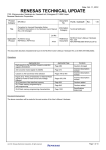
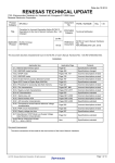
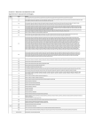
Date: Oct. 11, 2012 RENESAS TECHNICAL UPDATE 1753, Shimonumabe, Nakahara-ku, Kawasaki-shi, Kanagawa 211-8668 Japan Renesas Electronics Corporation Product Category Title MPU/MCU Document No. TN-RL*-A002A/E Correction for Incorrect Description Notice RL78/G12 Descriptions in the Hardware User’s Manual Rev. 1.00 Changed Information Category Technical Notification Reference Document RL78/G12 User’s Manual: Hardware Rev. 1.00 R01UH0200EJ0100 (Mar. 2012) Rev. 1.00 Lot No. Applicable Product RL78/G12 Group R5F102xxx, R5F103xxx All lot This document describes misstatements found in the RL78/G12 User’s Manual: Hardware Rev. 1.00 (R01UH0200EJ0100). Corrections Applicable Item 1.1 Differences of 1.1 RL78/G12 products (R5F102 and R5F103) 1.6 Outline of Functions Figure 3-1. Memory Map for the R5F10266 and R5F10366 Cautions on internal data memory space/control register/general-purpose register Figure 3-8. Correspondence Between Data Memory and Addressing for the R5F10266 and R5F10366 High-speed on-chip oscillator frequency selection register (HOCODIV) Applicable Page Pages 1 and 2 Outline added Page 11 Cautions added Page 24 Cautions added Pages 36, 44, 46 Explanations added Page 38 Cautions added Page 155 Cautions changed A/D converter mode register 0 (ADM0) Page 297 A/D conversion time selection Pages 302, 304 Figure 19-2. Timing of Generation of Internal Reset Signal by Power-on-reset Circuit and Voltage Detector 24.4 Overview of the data flash memory Page 722 24.6 Security Settings Page 729 Table 24-12. Security Setting in Each Programming Mode 24.7 Flash memory programming by self-programming Contents Pages 670, 671 Incorrect descriptions revised Incorrect descriptions revised Incorrect descriptions revised Cautions added Incorrect descriptions revised Page 730 Deleted Page 731 Cautions added 24.7.1 Flash shield window function Page 733 28.8 Flash memory programming characteristics Page 804 Incorrect descriptions revised Specifications determined Document Improvement The above corrections will be made for the next revision of the User’s Manual: Hardware. (c) 2012. Renesas Electronics Corporation. All rights reserved. Page 1 of 26 Date: Oct. 11, 2012 RENESAS TECHNICAL UPDATE TN-RL*-A002A/E Corrections in the User’s Manual: Hardware No. 1 2 3 4 5 6 7 8 9 10 11 12 13 14 15 Corrections and Applicable Items Document No. English R01UH0200EJ0100 1.1 Outline for differences of the RL78/G12 Pages 1, 2 (R5F102 and R5F103) added Cautions on Outline of Functions added Page 11 Cautions for Figure 3-1. Memory Map Pages 24 (R5F10266, R5F10366) added Explanations for cautions on internal data memory space/control Pages 36, 44, 46 register/general-purpose register added Cautions on Figure 3-8. Correspondence Between Data Memory and Addressing for Page 38 the R5F10266 and R5F10366 added Cautions on the high-speed on-chip oscillator frequency selection register Page 155 (HOCODIV) changed Incorrect descriptions of A/D converter Page 297 mode register 0 (ADM0) revised Incorrect descriptions of A/D conversion Pages 302, 304 time selection revised Incorrect descriptions of Figure 19-2. Timing of Generation of Internal Reset Signal by Pages 670, 671 Power-on reset Circuit and Voltage Detector revised Cautions on 24.4 Overview of the data flash Page 722 memory added Incorrect descriptions of 24.6 Security Page 729 Settings revised Table 24-12. Security Setting in Each Page 730 Programmable Mode deleted Cautions on 24.7 Flash Memory Page 731 Programming by Self-Programming added Incorrect descriptions of 24.7.1 Flash shield Page 733 window function revised Specifications of 28.8 Flash Memory Page 804 Programming Characteristics determined Pages in this document for corrections Pages 3, 4 Page 5, 6 Page 7 Page 8 Page 9 Page 10 Page 11 Pages 12 to 15 Pages 16 to 19 Page 20 Page 21 Page 22 Page 23 Page 24 Page 25 Incorrect: Bold with underline, Correct: Gray hatched Page 2 of 26 Date: Oct. 11, 2012 RENESAS TECHNICAL UPDATE TN-RL*-A002A/E 1. Outline for differences of the RL78/G12 (R5F102 and R5F103) added Differences between the R5F102 and R5F103 (pages 1, 2) Addition: CHAPTER 1 OUTLINE 1.1 Differences between the R5F102 and R5F103 Differences between the R5F102 and R5F103 of the RL78/G12 are as follows: Data flash mounted/not mounted High-speed on-chip oscillator oscillation frequency accuracy Number of channels of the serial interface DMA function mounted/not mounted Safety function mounted/not mounted 1.1.1 Data Flash The R5F102 mounts 2KB data flash and the R5F103 does not mount the data flash. Part Number Data Flash R5F102 2KB R5F1026A, R5F1027A, R5F102AA, R5F10269, R5F10279, R5F102A9, R5F10268, R5F10278, R5F102A8, R5F10267, R5F10277, R5F102A7, R5F10266 Note R5F103 Not mounted R5F1036A, R5F1037A, R5F103AA, R5F10369, R5F10379, R5F103A9, R5F10368, R5F10378 R5F103A8, R5F10367, R5F10377, R5F103A7, R5F10366 Note Since the R5F10266 includes small RAM size of 256 bytes, a stack area to execute the data flash library cannot be saved depending on the customer’s program specification and writing/erasing to the data flash may not be able to performed. Caution Since individual library is used when rewriting the flash memory using the user program, flash ROM and RAM areas are used. Refer to the RL78 Family Flash Self-Programming Library Type01 User’s Manual and RL78 Family Data Flash Library Type04 User’s Manual before using these products. Page 3 of 26 Date: Oct. 11, 2012 RENESAS TECHNICAL UPDATE TN-RL*-A002A/E 1.1.2 On-chip oscillator characteristics (1) High-speed on-chip oscillator oscillation frequency accuracy of the R5F102 Oscillator Condition High-speed on-chip oscillator oscillation frequency accuracy Min. Max. TA = – 20 to + 85 C –1 +1 TA = – 40 to – 20 C – 1.5 + 1.5 Min. Max. –5 +5 Unit % (2) High-speed on-chip oscillator oscillation frequency accuracy of the R5F103 Oscillator Condition Unit High-speed on-chip TA = – 40 to + 85 C oscillator oscillation % frequency accuracy 1.1.3 Peripheral functions There are differences of peripheral functions listed in the table below between the R5F102 and R5F103. R5F102 RL78/G12 20- and 24-pin products Serial Interface UART CSI 2 Simplified I C DMA Function Safety Function R5F103 30-pin products 20- and 24-pin products 1 channel 3 channels 1 channel 2 channels 3 channels 1 channel 2 channels 3 channels None 2 channels None CRC calculation Included None RAM guard Included None SFR guard Included None 30-pin products Page 4 of 26 Date: Oct. 11, 2012 RENESAS TECHNICAL UPDATE TN-RL*-A002A/E 2. Cautions on Outline of Functions added (Page 11) Incorrect: 1.6 Outline of Functions This outline describes the function at the time when Peripheral I/O redirection register (PIOR) is set to 00H (except timer output of 30-pin products with data flash) (1/2) Item 20-pin R5F1026x Code flash memory 24-pin R5F1036x R5F1027x 30-pin R5F1037x 2 KB RAM 256 B to 1.5 KB R5F103Ax 4 to 16 KB 2 to 16 KB Data flash memory R5F102Ax 2 KB Note 1 512 B to 1.5 KB 2 KB Note 1 512 B to 2KB 1 MB Memory space (Omitted) Timer 16-bit timer 4 channels Watchdog timer 1 channel 12-bit Interval timer Timer output Notes 1. 8 channels 1 channel 4/8 Note 2 (PWM Output Note 3 : 3/7 Note 2 ) This is about 639 bytes when the self-programming function and data flash function are used. (For details, see CHAPTER 3) 2. In 30-pin products with data flash, when setting to PIOR0 = 1. 3. The number of outputs varies, depending on the setting of channels in use and the number of the master (see 6.8.3 Operation as multiple PWM output function). Page 5 of 26 Date: Oct. 11, 2012 RENESAS TECHNICAL UPDATE TN-RL*-A002A/E Correct: 1.6 Outline of Functions This outline describes the function at the time when Peripheral I/O redirection register (PIOR) is set to 00H (except timer output of the R5F102Ax) (1/2) Item 20-pin R5F1026x Code flash memory Data flash memory RAM 2 to 16 KB 24-pin R5F1036x R5F1027x 30-pin R5F1037x Note 1 2 KB R5F102Ax R5F103Ax 4 to 16 KB 2 KB 256 B to 1.5 KB 512 B to 1.5 KB Address space 2 KB 512 B to 2KB 1 MB (Omitted) Timer 16-bit timer 4 channels Watchdog timer 1 channel 12-bit Interval timer Timer output Notes 1. 8 channels 1 channel 4/8 Note 2 (PWM Output Note 3 : 3/7 Note 2 ) The self-programming function cannot be used for the R5F10266 and R5F10366. 2. In the R5F102Ax, when setting to PIOR0 = 1. 3. The number of outputs varies, depending on the setting of channels in use and the number of the master (see 6.8.3 Operation as multiple PWM output function). Caution Since individual library is used when rewriting the flash memory using the user program, flash ROM and RAM areas are used. Confirm the RL78 Family Flash Self-Programming Library Type01 User’s Manual and RL78 Family Data Flash Library Type04 User’s Manual before using these products. Page 6 of 26 RENESAS TECHNICAL UPDATE TN-RL*-A002A/E Date: Oct. 11, 2012 3. Cautions for Memory Map (R5F10266, R5F10366) added (Page 24) Incorrect: Figure 3-1. Memory Map for the R5F10266 and R5F10366 (Omitted) Notes 1. Use of the area FFE20H to FFEFFH is prohibited when using the self-programming function and data flash function, because this area is used for self-programming library. (Omitted) Correct: Figure 3-1. Memory Map for the R5F10266 and R5F10366 (Omitted) Notes 1. When rewriting the data flash, allocate the stack used for the data flash library to FFEA2H to FFEDFH, and the RAM address used for the data flash and DMA transfer to FFE00H to FFE19H. Fore more details, refer to the RL78 Family Data Flash Library Type04 User’s Manual. (Omitted) Cautions 2. Since the R5F10266 includes small RAM size of 256 bytes, a stack area to execute the data flash library cannot be saved depending on the customer’s program specification and writing/erasing to the data flash may not be able to be performed. For more details, refer to the RL78 Family Data Flash Library Typ04 User’s Manual. 3. The self-programming function cannot be used for the R5F10266 and R5F10366. Page 7 of 26 Date: Oct. 11, 2012 RENESAS TECHNICAL UPDATE TN-RL*-A002A/E 4. Explanations for cautions on internal data memory space/control register/general-purpose register added (Pages 36, 44, 46) Incorrect: Cautions 1. It is prohibited to use the general-purpose register space (FFEE0H to FFEFFH) for fetching instructions or as a stack area. 2. The internal RAM in the following products cannot be used as stack memory when using the self-programming function and data flash function (refer to figure 3-1 to 3-6 Memory Map). R5F10x66, R5F10x67, R5F10x77, R5F10xA7, : FFE20H-FFEFFH R5F10xA8, R5F10xA9, R5F10xAA R5F10x68, R5F10x78: FFE20H to FFEFFH, FFC00H to FFC80H R5F10x69, R5F10x79: FFE20H to FFEFFH, FFB00H to FFC80H R5F10x6A, R5F10x7A: FFE20H to FFEFFH, FF900H to FFC80H (x = 2, 3) Correct: (Omitted) Cautions 1. It is prohibited to use the general-purpose register space (FFEE0H to FFEFFH) for fetching instructions or as a stack area. 2. When self-programming or rewriting the data flash, do not allocate the stack used by individual library and RAM address used for the data buffer and DMA transfer to RAM areas of the products shown below. For more details, refer to the RL78 Family Flash Self-Programming Library Type01 User’s Manual and RL78 Family Data Flash Library Type04 User’s Manual. R5F10266 : FFE20H to FFEA1H, FFEE0H to FFEFFH (Allocate the stack used for the data flash library to FFEA2H to FFEDFH, and the RAM address used for the data buffer and DMA transfer to FFE00H to FFE19H.) R5F102mn, R5F103mn : FFE20H to FFEFFH m: Pin count symbol (m = 6, 7, A), n: ROM size symbol (n = 7, 8, 9, A) 3. Since RAM areas of the products shown below is used for the self-programming library and data flash library, its area cannot be used (refer to Figures 3-3 to 3-5 Memory Map). R5F102m8, R5F103m8 : FFC00H-FFC80H R5F102m9, R5F103m9 : FFB00H-FFC80H R5F102mA, R5F103mA : FF900H-FFC80H m: Pin count symbol (m = 6, 7) Page 8 of 26 RENESAS TECHNICAL UPDATE TN-RL*-A002A/E Date: Oct. 11, 2012 5. Cautions on Correspondence Between Data Memory and Addressing (R5F10266, R5F10366) added (page 38) Incorrect: Figure 3-8. Correspondence between Data Memory and Addressing for the R5F10266 and R5F10366 (Omitted) Notes 1. FFE20H to FFEFFH area used by the self-programming libraries cannot be used when the self-programming function and data flash function are used. (Omitted) Correct: Figure 3-8. Correspondence between Data Memory and Addressing for the R5F10266 and R5F10366 Notes 1. When rewriting the data flash, allocate the stack used for the data flash library to FFEA2H to FFEDFH, and RAM address for the data buffer and DMA transfer to FFE00H to FFE19H. For more details, refer to the RL78 Family Data Flash Library Type04 User’s Manual. (Omitted) Cautions 2. Since the R5F10266 includes small RAM size of 256 bytes, a stack area to execute the data flash library cannot be saved depending on the customer’s program specification and writing/erasing to the data flash may not be able to be performed. For more details, refer to the RL78 Family Data Flash Library Typ04 User’s Manual. 3. The self-programming function cannot be used for the R5F10266 and R5F10366. Page 9 of 26 Date: Oct. 11, 2012 RENESAS TECHNICAL UPDATE TN-RL*-A002A/E 6. Cautions on the high-speed on-chip oscillator frequency selection register (HOCODIV) changed (page 155) Incorrect: (8) High-speed on-chip oscillator frequency selection register (HOCODIV) (Omitted) Cautions 1. Set the HOCODIV register within the operable voltage range before and after the frequency change. 2. When the frequency is changed with the HOCODIV register, use it within the voltage range of the flash operation mode set in the option byte (000C2H). Option byte (000C2H) value Flash operation mode CMODE1 CMODE2 1 0 LS (low-speed main) mode 1 1 HS (high-speed main) mode Operating frequency Operating voltage range range 1 MHz to 8 MHz 1.8 V to 5.5 V 1 MHz to 16 MHz 2.4 V to 5.5 V 1 MHz to 24 MHz 2.7 V to 5.5 V 3. The device operates at the old frequency for the duration of 3 clocks after the frequency value has been changed by using the HOCODIV register. When setting of high-speed on-chip oscillator clock as system clock, and the clock oscillation stabilization wait three minutes further. 4. When changing the frequency of the high-speed on-chip oscillator while X1 oscillation/external oscillation input is set to the system clock, after set the bit 0 (HIOSTOP) of the CSC register to 1, to stop the high-speed on-chip oscillator. Correct: (8) High-speed on-chip oscillator frequency selection register (HOCODIV) (Omitted) Cautions 1. Set the HOCODIV register within the operable voltage range of the flash operation mode set in the option byte (000C2H) before and after the frequency change. Option byte (000C2H) value CMODE1 CMODE2 1 0 1 1 Operating frequency Operating voltage range range LS (low-speed main) mode 1 MHz to 8 MHz 1.8 V to 5.5 V HS (high-speed main) mode 1 MHz to 16 MHz 2.4 V to 5.5 V 1 MHz to 24 MHz 2.7 V to 5.5 V Flash operation mode 2. Set the HOCODIV register while the high-speed on-chip oscillator clock (fIH) is selected as the CPU/peripheral hardware clock (fCLK). 3. After the frequency has been changed using the HOCODIV register and the following transition time has been elapsed, the frequency is switched. The device operates at the frequency for the duration of 3 clocks before the frequency has been changed. The CPU/peripheral hardware clock waits for maximum 3 clocks at the frequency after the frequency has been changed. Page 10 of 26 RENESAS TECHNICAL UPDATE TN-RL*-A002A/E Date: Oct. 11, 2012 7. Incorrect descriptions of A/D converter mode register 0 (ADM0) revised (page 297) Incorrect: (2) A/D converter mode register 0 (ADM0) (Omitted) Cautions 1. Change the ADMD, FR2 to FR0, LV1, LV0, and ADCE bits while conversion is stopped or on standby (ADCS = 0). 2. Do not change the ADCE and ADCS bits from 0 to 1 at the same time by using an 8-bit manipulation instruction. Be sure to set these bits in the order described in 10.7 A/D Converter Setup Flowchart. Correct: (2) A/D converter mode register 0 (ADM0) (Omitted) Cautions 1. Change the ADMD, FR2 to FR0, LV1, and LV0 bits while conversion is stopped (ADCS = 0, ADCE = 0). 2. Do not set ADCS = 1 and ADCE = 0. 3. Do not change the ADCS and ADCE bits from 0 to 1 at the same time by using an 8-bit manipulation instruction. Be sure to set these bits in the order described in 10.7 A/D Converter Setup Flowchart. Page 11 of 26 Date: Oct. 11, 2012 RENESAS TECHNICAL UPDATE TN-RL*-A002A/E 8. Incorrect descriptions of A/D conversion time selection revised (pages 302 and 304) Incorrect: Table 10-3. A/D Conversion Time Selection (2) Low voltage ModeNote 1 When there is no stabilization wait time (software trigger mode/hardware trigger no-wait mode) A/D Converter Mode Mode Conversion Number of Conversion Register 0 (ADM0) Clock (fAD) Conversion Clock FR2 FR1 FR0 LV1 LV0 0 0 1 0 Low 0 fCLK/32 voltage 0 1 0 0 1 1 1 fCLK/16 fCLK/8 19 fAD (Number of Conversion Time Selection Time 608/fCLK sampling 304/fCLK clock : 7 152/fCLK 1.8 V VDD 5.5 V Note 2 fCLK = fCLK = fCLK = fCLK = fCLK = fCLK = 1 MHz 2 MHz 4 MHz 8 MHz 16 MHz 24 MHz Setting Setting Setting 76 s prohibited prohibited prohibited 76 s 76 s 38 s 38 s 19 s 0 0 fCLK/6 57 s 114/fCLK 28.5 s 14.25 s Note 4 1 1 1 0 0 1 1 0 1 fCLK/5 0 1 1 0 0 1 1 76/fCLK fCLK/2 0 Low 1 fCLK/32 voltage 0 95/fCLK fCLK/4 1 2 fCLK/16 fCLK/8 38/fCLK 17 fAD (Number of 544/fCLK sampling 272/fCLK clock : 5 136/fCLK 95 s 47.5 s 23.75 s 11.875 s 0 0 1 1 0 1 1 1 0 1 Other than the above 12.67 s 9.5 s 6.33 s 7.125s 4.75 s Note 4 5.938 s 3.96 s 9.5 s 4.75 s 3.17 s Note 4 Note 4 Note 5 9.5 s 4.75 s 2.375s Note 4 Note 4 Note 5 Setting prohibited Setting Setting Setting 68 s prohibited prohibited prohibited 34 s 22.667 s 17 s 11.333 s 8.5 s 5.667 s 76 s 38 s 38 s 19 s 68 s 19 s 68 s 34 s 34 s 17 s Note 4 fCLK/6 51 s 102/fCLK fCLK/5 85/fCLK fCLK/4 68/fCLK fCLK/2 19 s Note 4 25.5 s 12.75 s Note 4 1 25.33 s Note 4 fAD) 1 38 s Note 4 fAD) 1 Note 3 34/fCLK 85 s 68 s 34 s 42.5 s 34 s 17 s 21.25 s 10.625 s 17 s 6.375 s 4.25 s Note 4 5.313 s 3.542 s Note 4 Note 4 8.5 s 4.25 s 2.833s Note 4 Note 4 Note 5 Setting prohibited 8.5 s 4.25 s 2.125 s Note 4 Note 4 Note 5 Setting prohibited Page 12 of 26 Date: Oct. 11, 2012 RENESAS TECHNICAL UPDATE TN-RL*-A002A/E (4) Low voltage ModeNote 1 When there is stabilization wait time Note 2 (hardware trigger wait mode) A/D Converter Mode Mode Conversion Number of Number of Stabilization Register 0 (ADM0) Clock (fAD) FR2 FR1 FR0 LV1 LV0 0 0 1 0 0 wait clock fCLK/32 2 fAD voltage 0 1 0 0 1 1 Clock Conversion Time Low 1 Stabilization Wait Time + Conversion Time Selection stabilization Conversion Wait Time + 19 fAD (Number of fCLK/16 fCLK/8 672/fCLK sampling 336/fCLK clock :7 168/fCLK 1.8 V VDD 5.5 V Note3 fCLK = fCLK = fCLK = fCLK = fCLK = fCLK = 1 MHz 2 MHz 4 MHz 8 MHz 16 MHz 24 MHz Setting Setting Setting prohibited prohibited prohibited 84 s 84 s 42 s 28 s 84 s 42 s 21 s 14 s 42 s 21 s 10.5 s 7 s Note 5 fAD) 1 1 1 1 0 0 0 1 1 0 0 fCLK/6 1 1 105/fCLK fCLK/4 1 84/fCLK fCLK/2 0 1 Low 42/fCLK fCLK/32 17 fAD voltage 0 0 1 1 0 2 1 63 s 126/fCLK fCLK/5 0 (Number of fCLK/16 sampling clock :5 fCLK/8 608/fCLK 105 s 84 s 42 s 52.5 s 42 s 21 s 31.25 s 26.25 s 76 s 13.125s 6.563 s Note 5 Note 5 1 1 1 0 0 1 1 0 95/fCLK fCLK/4 1 76/fCLK fCLK/2 Other than the above 57 s 114/fCLK fCLK/5 0 38/fCLK 4.38 s 5.25 s 3.5 s Note 5 Note 6 10.5 s 5.25 s 2.625 s Note 5 Note 5 Note 6 Setting prohibited 76 s 38s 25.33 s 38 s 19s 38 s 19s 9.5 s 12.67 s Note 6.33 s 5 fCLK/6 1 5.25 s 10.5 s 76 s 152/fCLK 7.875 s Note 5 Note 5 21 s Setting Setting Setting prohibited prohibited prohibited 304/fCLK 15.75 s Note 5 fAD) 1 Note4 95 s 76 s 38 s 47.5 s 38 s 19 s 28.5 s 23.75 s 14.25s 7.125 s Note 5 Note 5 11.875 s 5.938 s Note 5 Note 5 4.75 s 3.96 s 9.5 s 4.75s 3.17 s Note 5 Note 5 Note 6 9.5 s 4.75s 2.375 s Note 5 Note 5 Note 6 Setting prohibited 19 s Setting prohibited (Omitted) Cautions 1. When rewriting the FR2 to FR0, LV1, and LV0 bits to other than the same data, stop A/D conversion once (ADCS = 0) beforehand. Page 13 of 26 Date: Oct. 11, 2012 RENESAS TECHNICAL UPDATE TN-RL*-A002A/E Correct: Table 10-3. A/D Conversion Time Selection (2) Low voltage ModeNote 1 When there is no stabilization wait time (software trigger mode/hardware trigger no-wait mode) A/D Converter Mode Mode Conversion Number of Conversion Register 0 (ADM0) Clock (fAD) Conversion 0 1 1 Low 0 fCLK/32 voltage 0 1 0 0 1 1 1.8 V VDD 5.5 V Clock FR2 FR1 FR0 LV1 LV0 0 Conversion Time Selection Time 1 fCLK/16 fCLK/8 19 fAD (Number of 608/fCLK sampling 304/fCLK clock : 7 152/fCLK Note 2 fCLK = fCLK = fCLK = fCLK = fCLK = fCLK = 1 MHz 2 MHz 4 MHz 8 MHz 16 MHz 24 MHz Setting Setting Setting 76 s prohibited prohibited prohibited 76 s 0 0 1 1 0 0 38 s 19 s 12.67 s 19 s 9.5 s 6.33 s Note 4 fCLK/6 1 1 0 1 57 s 114/fCLK fCLK/5 0 1 1 0 0 1 1 76/fCLK fCLK/2 1 Low 1 fCLK/32 voltage 0 95/fCLK fCLK/4 1 2 fCLK/16 fCLK/8 28.5 s 14.25 s 38/fCLK 17 fAD (Number of 544/fCLK sampling 272/fCLK clock : 5 136/fCLK 95 s 47.5 s 23.75 s 11.875 s 0 0 1 1 0 1 1 1 0 1 Other than the above 4.75 s 3.96 s 9.5 s 4.75 s 3.17 s Note 4 Note 4 Note 5 9.5 s 4.75 s 2.375s Note 4 Note 4 Note 5 Setting prohibited Setting Setting Setting 68 s prohibited prohibited prohibited 34 s 22.667 s 17 s 11.333 s 8.5 s 5.667 s 76 s 38 s 38 s 19 s 68 s 19 s 68 s 34 s 34 s 17 s Note 4 fCLK/6 51 s 102/fCLK fCLK/5 85/fCLK fCLK/4 68/fCLK fCLK/2 5.938 s Note 4 25.5 s 12.75 s Note 4 1 7.125s Note 4 Note 4 fAD) 1 25.33 s 38 s Note 4 1 38 s 76 s fAD) 1 Note 3 34/fCLK 85 s 68 s 34 s 42.5 s 34 s 17 s 21.25 s 10.625 s 17 s 6.375 s 4.25 s Note 4 5.313 s 3.542 s Note 4 Note 4 8.5 s 4.25 s 2.833s Note 4 Note 4 Note 5 Setting prohibited 8.5 s 4.25 s 2.125 s Note 4 Note 4 Note 5 Setting prohibited (Omitted) Cautions 1. Rewrite the FR2 to FR0, LV1, and LV0 bits to other than the same data while conversion is stopped (ADCS = 0, ADCE = 0). Page 14 of 26 Date: Oct. 11, 2012 RENESAS TECHNICAL UPDATE TN-RL*-A002A/E (4) Low voltage ModeNote 1 When there is stabilization wait time Note 2 (hardware trigger wait mode) A/D Converter Mode Mode Conversion Number of Number of Stabilization Register 0 (ADM0) Clock (fAD) FR2 FR1 FR0 LV1 LV0 0 0 1 1 0 wait clock fCLK/32 2 fAD voltage 0 1 0 0 1 1 Clock Conversion Time Low 1 Stabilization Wait Time + Conversion Time Selection stabilization Conversion Wait Time + 19 fAD (Number of fCLK/16 fCLK/8 672/fCLK sampling 336/fCLK clock :7 168/fCLK 1.8 V VDD 5.5 V Note3 fCLK = fCLK = fCLK = fCLK = fCLK = fCLK = 1 MHz 2 MHz 4 MHz 8 MHz 16 MHz 24 MHz Setting Setting Setting prohibited prohibited prohibited 84 s 84 s 42 s 28 s 84 s 42 s 21 s 14 s 42 s 21 s 10.5 s 7 s Note 5 fAD) 1 1 1 1 0 0 0 1 1 0 0 fCLK/6 1 1 105/fCLK fCLK/4 1 84/fCLK fCLK/2 1 1 Low 42/fCLK fCLK/32 17 fAD voltage 0 0 1 1 0 2 1 63 s 126/fCLK fCLK/5 0 (Number of fCLK/16 sampling clock :5 fCLK/8 608/fCLK 105 s 84 s 42 s 52.5 s 42 s 21 s 31.25 s 26.25 s 76 s 13.125s 6.563 s Note 5 Note 5 1 1 1 0 0 1 1 0 95/fCLK fCLK/4 1 76/fCLK fCLK/2 Other than the above 57 s 114/fCLK fCLK/5 0 38/fCLK 4.38 s 5.25 s 3.5 s Note 5 Note 6 10.5 s 5.25 s 2.625 s Note 5 Note 5 Note 6 Setting prohibited 76 s 38s 25.33 s 38 s 19s 38 s 19s 9.5 s 12.67 s Note 6.33 s 5 fCLK/6 1 5.25 s 10.5 s 76 s 152/fCLK 7.875 s Note 5 Note 5 21 s Setting Setting Setting prohibited prohibited prohibited 304/fCLK 15.75 s Note 5 fAD) 1 Note4 95 s 76 s 38 s 47.5 s 38 s 19 s 28.5 s 23.75 s 14.25s 7.125 s Note 5 Note 5 11.875 s 5.938 s Note 5 Note 5 4.75 s 3.96 s 9.5 s 4.75s 3.17 s Note 5 Note 5 Note 6 9.5 s 4.75s 2.375 s Note 5 Note 5 Note 6 Setting prohibited 19 s Setting prohibited (Omitted) Cautions 1. Rewrite the FR2 to FR0, LV1, and LV0 bits to other than the same data while conversion is stopped (ADCS = 0, ADCE = 0). Page 15 of 26 Date: Oct. 11, 2012 RENESAS TECHNICAL UPDATE TN-RL*-A002A/E 9. Incorrect descriptions of the power-on reset circuit on Figure 19-2 revised (pages 670 and 671) Incorrect: Figure 19-2. Timing of Generation of Internal Reset Signal by Power-on-reset Circuit and Voltage Detector (a) When LVD is OFF (option byte 000C1H: VPOC2 = 1) Supply voltage (VDD) Operating voltage range lower limit setting VPOR = 1.51 V (TYP.) VPDR = 1.50 V (TYP.) 0V 10 s min. 10 s min. External RESET signal Wait for oscillation Note 1 accuracy stabilization Wait for oscillation Note 1 accuracy stabilization High-speed on-chip oscillator clock (fIH) Starting oscillation is specified by software High-speed system clock (fMX) (when X1 oscillation is selected) CPU Starting oscillation is specified by software Reset processingNote 3 Operation stops Normal operation (high-speed on-chip oscillator clock)Note 2 Reset period (oscillation stop) Reset processingNote 3 Normal operation (high-speed on-chip oscillator clock)Note 2 Operation stops Internal reset signal (Omitted) Notes 3. Reset processing time: 265 to 407 s (b) When LVD is interrupt & reset mode (option byte 000C1H/LVIMDS1, LVIMDS0 = 1, 0) Supply voltage (VDD) Note 3 VLVDH VLVDL 1.8 V VPOR= 1.51V (TYP.) VPDR= 1.50V (TYP.) 0V Wait for oscillation accuracy stabilization Note 2 High-speed on-chip oscillator clock (fIH) High-speed system clock (fMX) (when X1 oscillation is selected) CPU Operation stops Wait for oscillation accuracy stabilization Note 2 Starting oscillation is speci ed by software Starting oscillation is specied b y software Normal operation (High-speed on-chip oscillator clock)Note 1 Reset processing timeNote 4 Reset period (oscillation stop) Normal operation (High-speed on-chip oscillator clock)Note 1 Reset processing timeNote 4 Operation stops POR proc essing time POR proc essing time Internal reset signal INTLVI (Omitted) Notes 4. Reset processing time: 497 to 720 s Page 16 of 26 Date: Oct. 11, 2012 RENESAS TECHNICAL UPDATE TN-RL*-A002A/E Correct: Figure 19-2. Timing of Generation of Internal Reset Signal by Power-on-reset Circuit and Voltage Detector (1) When the external reset input via RESET pin is used Supply voltage (VDD) Operating voltage range lower limit setting VPOR = 1.51 V (TYP.) VPDR = 1.50 V (TYP.) 0V RESET signal 10 s min. 10 s min. Wait for oscillation accuracy stabilizationNote 1 Wait for oscillation Note 1 accuracy stabilization High-speed on-chip oscillator clock (fIH) High-speed system clock (fMX) (when X1 oscillation is selected) CPU Operation stops Starting oscillation is specified by software Starting oscillation is specified by software Reset processing time Note 3 by the external reset release Normal operation (high-speed on-chip oscillator clock)Note 2 Reset period (oscillation stop) Reset processing time Note 3 by the external reset release Normal operation (high-speed on-chip oscillator clock)Note 2 Operation stops Voltage stabilization wait time 0.99 ms (TYP.), 2.30 ms (MAX.) Voltage stabilization wait time 0.99 ms (TYP.), 2.30 ms (MAX.) Internal reset signal (Omitted) Notes 3. The time until normal operation is started require the following “the reset processing time by the external reset release” required after RESET signal has been set to high-level(1), in addition to “the voltage stabilization wait time” required after the voltage has reached VPOR (1.51 V (TYP.)). Reset processing time by the external reset release: 0.672 ms (TYP.), 0.832 ms (MAX.) (When LVD is used) 0.399 ms (TYP.), 0.519 ms (MAX.) (When LVD off) Page 17 of 26 Date: Oct. 11, 2012 RENESAS TECHNICAL UPDATE TN-RL*-A002A/E (2) LVD interrupt & reset mode (option byte 000C1H/LVIMDS1, LVIMDS0 = 1, 0) Supply voltage (VDD) Note 3 VLVDH VLVDL Operating voltage range lower limit setting VPOR = 1.51 V (TYP.) VPDR = 1.50 V (TYP.) 0V Wait for oscillation accuracy stabilizationNote 2 Wait for oscillation accuracy stabilizationNote 2 High-speed on-chip oscillator clock (fIH) High-speed system clock (fMX) (when X1 oscillation is selected) CPU Operation stops Starting oscillation is specified by software Normal operation (high-speed on-chip oscillator clock)Note 1 Reset processing timeby LVD Reset period (oscillation stop) Normal operation (high-speed on-chip oscillator clock)Note 1 Operation stops Reset processing timeby LVDNote 4 Note 4 Voltage stabilization wait time and reset processing timeby POR 1.64 ms(TYP.), 3.10 msMAX.) ( Voltage stabilization wait time and reset processing timeby POR 1.64 ms(TYP.), 3.10 msMAX.) ( Internal reset signal INTLVI (Omitted) Note 4. The time until normal operation is started require the following “the reset processing time by LVD” required after the voltage has reached LVD detection level (VLVDH), in addition to “the reset processing time by POR” and “the voltage stabilization wait time” required after the voltage has reached VPOR (1.51 V (TYP.)). Reset processing time by LVD: 0 ms to 0.0701 ms (MAX.) Page 18 of 26 Date: Oct. 11, 2012 RENESAS TECHNICAL UPDATE TN-RL*-A002A/E (3) LVD reset mode (option byte 000C1H/LVIMDS1, LVIMDS0 = 1, 1) Supply voltage (VDD) VLVD Operating voltage range lower limit setting VPOR = 1.51 V (TYP.) VPDR = 1.50 V (TYP.) 0V Wait for oscillation accuracy stabilizationNote 2 Wait for oscillation accuracy stabilizationNote 2 Wait for oscillation accuracy stabilizationNote 2 High-speed on-chip oscillator clock (fIH) High-speed system clock (fMX) (when X1 oscillation is selected) CPU Operation stops Normal operation (high-speed on-chip oscillator clock)Note 1 Reset period (oscillation stop) Normal operation (high-speed on-chip oscillator clock)Note 1 Reset period (oscillation stop) Reset processing timeby LVD Operation stops Reset processing timeby LVD Note 3 Voltage stabilization wait time and Reset processing timeby POR 1.64 ms(TYP.), 3.10 msMAX.) ( Normal operation (high-speed on-chip oscillator clock)Note 1 Note 3 Reset processing timeby LVDNote 4 Voltage stabilization wait time and Reset processing timeby POR 1.64 ms(TYP.), 3.10 msMAX.) ( Internal reset signal (Omitted) Note 3. The time until normal operation is started require the following “the reset processing time by LVD” required after the voltage has reached LVD detection level (VLVD), in addition to “the reset processing time by POR” and “the voltage stabilization wait time” required after the voltage has reached VPOR (1.51 V (TYP.)). Reset processing time by LVD: 0 ms to 0.0701 ms (MAX.) 4. When supply voltage falls and returns after only an internal reset occurs by the voltage detection circuit (LVD), the following “the reset processing time by LVD” is required after the voltage has reached LVD detection level (VLVD). Reset processing time by LVD: 0.0629 ms (TYP.), 0.0701 ms (MAX.) Page 19 of 26 RENESAS TECHNICAL UPDATE TN-RL*-A002A/E Date: Oct. 11, 2012 10. Cautions on overview of the data flash memory added (page 722) Incorrect: An overview of the data flash memory is provided below. The data flash memory can be written to by using the flash memory programmer or an external device Programming is performed in 8-bit units Blocks can be deleted in 1 KB units The only access by CPU instructions is byte reading (4 clock + wait 3 clock cycles) Because the data flash memory is an area exclusively used for data, it cannot be used to execute instructions (code fetching) Instructions can be executed from the code flash memory while rewriting the data flash memory (That is, Back Ground Operation (BGO) is supported) Accessing the data flash memory is not possible while rewriting the code flash memory (during self programming) Because the data flash memory is stopped after a reset ends, the data flash control register (DFLCTL) must be set up in order to use the data flash memory Manipulating the DFLCTL register is not possible while rewriting the data flash memory Transition the HALT, STOP mode is not possible while rewriting the data flash memory Correct: An overview of the data flash memory is provided below. For more details of rewriting the data flash memory, refer to the RL78 Family Data Flash Library Type04 User’s Manual. The data flash memory can be written to by using the flash memory programmer or an external device Programming is performed in 8-bit units Blocks can be deleted in 1 KB units The only access by CPU instructions is byte reading (1 clock + wait 3 clock cycles) Because the data flash memory is an area exclusively used for data, it cannot be used to execute instructions (code fetching) Instructions can be executed from the code flash memory while rewriting the data flash memory (That is, Back Ground Operation (BGO) is supported) Accessing the data flash memory is not possible while rewriting the code flash memory (during self programming) Because the data flash memory is stopped after a reset ends, the data flash control register (DFLCTL) must be set up in order to use the data flash memory Manipulating the DFLCTL register is not possible while rewriting the data flash memory Transition the HALT, STOP mode is not possible while rewriting the data flash memory Cautions 1. While the data flash is being rewritten, interrupts are disabled only for the R5F10266. Execute the data flash library in the state where the IE flag is cleared (0) by the DI instruction. 2. The high-speed on-chip oscillator needs to oscillate while the data flash is being rewritten. When stopping the high-speed on-chip oscillator, oscillate the high-speed on-chip oscillator clock (HIOSTOP = 0) and execute the data flash library after 30 s elapses. Page 20 of 26 RENESAS TECHNICAL UPDATE TN-RL*-A002A/E Date: Oct. 11, 2012 11. Incorrect descriptions of Security Settings revised (page 729) Incorrect: 24.6 Security Settings The RL78/G12 supports a security function that prohibits rewriting the user program written to the internal flash memory, so that the program cannot be changed by an unauthorized person. The operations shown below can be performed by using the Security Set command. (Omitted) The block erase, write, and rewriting boot cluster0 commands are enabled by default when the flash memory is shipped. Security can be set by on-board/off-board programming and self programming. The security settings can be used in combination. Table 24-11 shows the relationship between the erase and write commands when the RL78/G12 security function is enabled. Caution The security function of the flash programmer does not support self-programming. Correct: 24.6 Security Settings The RL78/G12 supports a security function that prohibits rewriting the user program written to the internal flash memory, so that the program cannot be changed by an unauthorized person. The operations shown below can be performed by using the Security Set command. (Omitted) The block erase, write, and rewriting boot cluster0 commands are enabled by default when the flash memory is shipped. Security can be set only by on-board/off-board programming. The security settings can be used in combination. Table 24-11 shows the relationship between the erase and write commands when the RL78/G12 security function is enabled. Caution The security function of the flash programmer does not support self-programming. Page 21 of 26 Date: Oct. 11, 2012 RENESAS TECHNICAL UPDATE TN-RL*-A002A/E 12. Security Settings in self-programming mode deleted (page 730) Incorrect: Table 24-12. Security Setting in Each Programming Mode (1) On-board/off-board programming Security Security Setting How to Disable Security Setting Prohibition of block erasure Use the GUI of dedicated flash memory Cannot be disabled after setting. Prohibition of writing programmer. Execute security release command Prohibition of rewriting boot cluster 0 Caution Cannot be disabled after setting. The security release command can be applied only when the security is not set as the block erase prohibition and the boot cluster 0 rewrite prohibition with code flash memory area and data flash memory area being blanks. (2) Self programming Security Security Setting Prohibition of block erasure Use the set sets information library. How to Disable Security Setting Cannot be disabled after setting. Execute the security release command Prohibition of writing during on-board/off-board programming. (The security setting cannot be disabled during self programming.) Prohibition of rewriting boot cluster 0 Cannot be disabled after setting. Correct: Table 24-12. Security Setting in Each Programming Mode (1) On-board/off-board programming Security Security Setting Prohibition of block erasure Use the GUI of dedicated flash memory Prohibition of writing programmer. Prohibition of rewriting boot cluster 0 Caution How to Disable Security Setting Cannot be disabled after setting. Execute security release command Cannot be disabled after setting. The security release command can be applied only when the security is not set as the block erase prohibition and the boot cluster 0 rewrite prohibition with code flash memory area and data flash memory area being blanks. Page 22 of 26 Date: Oct. 11, 2012 RENESAS TECHNICAL UPDATE TN-RL*-A002A/E 13. Cautions on Flash Memory Programming by Self-Programming added (page 731) Incorrect: 24.7 Flash Memory Programming by Self-Programming The RL78/G12 supports a self-programming function that can be used to rewrite the flash memory via a user program. Because this function allows a user application to rewrite the flash memory by using the RL78/G12 self-programming library, it can be used to upgrade the program in the field. Cautions 1. To prohibit an interrupt during self-programming, in the same way as in the normal operation mode, execute the self-programming library in the state where the IE flag is cleared (0) by the DI instruction. To enable an interrupt, clear (0) the interrupt mask flag to accept in the state where the IE flag is set (1) by the EI instruction, and then execute the self-programming library. (Omitted) Correct: The RL78/G12 supports a self-programming function that can be used to rewrite the flash memory via a user program. Because this function allows a user application to rewrite the flash memory by using the RL78/G12 self-programming library, it can be used to upgrade the program in the field. Cautions 1. Interrupts are disabled during self-programming. Execute the self-programming library in the state where the IE flag is cleared (0) by the DI instruction. (Omitted) 3. The high-speed on-chip oscillator needs to oscillate during self-programming. When stopping the high-speed on-chip oscillator, oscillate the high-speed on-chip oscillator clock (HIOSTOP = 0) and execute the self-programming library after 30 s elapses. 4. The self-programming function cannot be used for the R5F10266 and R5F10366. Page 23 of 26 Date: Oct. 11, 2012 RENESAS TECHNICAL UPDATE TN-RL*-A002A/E 14. Incorrect descriptions of the Flash shield window function revised (page 733) Incorrect: 24. 7.1 Flash shield window function (Omitted) The window range can be set by specifying the start and end blocks. The window range can be set or changed during both on-board/off-board programming and self programming. (Omitted) Figure 24-14. Setting and changing of the flash shield window function and relations with commands Programming Setting/Changing window condition range Execution command Block erasure Writing During Specify the start block Block erasure can be Writing can be done self-programming and end block of the done only in the only in the window window in the set flash window range. range. self programming. During Specify the start block Block erasure can be Writing can be done on-board/off-board and end block of the done also outside the also outside the programming window on the GUI of the window range. window range. dedicated flash memory programmer. Note To prohibit writing and erasing during on-board/off-board programming, refer to "24.6 Security Settings." Correct: 24. 7.1 Flash shield window function (Omitted) The window range can be set by specifying the start and end blocks. The window range can be set or changed only during on-board/off-board programming. (Omitted) Figure 24-14. Setting and changing of the flash shield window function and relations with commands Programming Setting/Changing window condition range Execution command Block erasure Writing During Specify the start block Block erasure can be Writing can be done on-board/off-board and end block of the done also outside the also outside the programming window on the GUI of the window range. window range. dedicated flash memory programmer. Note To prohibit writing and erasing during on-board/off-board programming, refer to "24.6 Security Settings." Page 24 of 26 Date: Oct. 11, 2012 RENESAS TECHNICAL UPDATE TN-RL*-A002A/E 15. Specifications of the Flash Memory Programming Characteristics determined (page 804) Incorrect: 28.8 Flash Memory Programming Characteristics (TA = 40 to +85C, 1.8 V VDD 5.5 V, VSS = 0 V) Parameter Symbol Conditions MIN. System clock frequency fCLK 1.8 V VDD 5.5 V Code flash memory rewritable times Cerwr 1 erase + 1 write after Retained for 20 the erase is regarded years (Self/serial as 1 rewrite. programming) The retaining years Retained for 1 Data flash memory rewritable times TYP. 1 MAX. Unit 24 MHz 1,000 Times Note are until next rewrite after the rewrite. 1,000,000 years (Self/serial Note programming) Retained for 5 100,000 years (Self/serial Note programming) Note When using flash memory programmer and Renesas Electronics self programming library. Caution This specifications show target values, which may change after device evaluation. Correct: 28.8 Flash Memory Programming Characteristics (TA = 40 to +85C, 1.8 V VDD 5.5 V, VSS = 0 V) Parameter System clock frequency Code flash memory rewritable times Symbol fCLK Cerwr Conditions MIN. 1.8 V VDD 5.5 V TYP. 1 Retaining years: 20 years Ta = 85 C Note 3 Retaining year: 1 year Ta = 25 C Note 3 Retaining years: 5 years Ta = 85 C Note 3 100,000 Retaining years: 20 years Ta = 85 C Note 3 10,000 1,000 MAX. Unit 24 MHz Times Note 1,2,3 Data flash memory rewritable times 1,000,000 Note 1,2,3 Notes 1. 1 erase + 1 write after the erase is regarded as 1 rewrite. The retaining years are until next rewrite after the rewrite. 2. When using flash memory programmer and Renesas Electronics self programming library. 3. This characteristics is shown as the flash memory characteristics and based on Renesas Electronics reliability test. Page 25 of 26 RENESAS TECHNICAL UPDATE TN-RL*-A002A/E Date: Oct. 11, 2012 Issued Document History RL78/G12 User’s Manual: Hardware Rev 1.00, incorrect description notice, issued document history Document Number TN-RL*- A002A /E Issue Date Oct. 11, 2012 Description First edition issued Incorrect descriptions of No.1 to No.15 revised Page 26 of 26