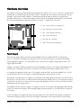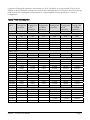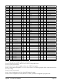
1
Danville Signal Processing, Inc.
dspblok™ 21369zx
User Manual
Version 1.01
Danville Signal Processing, Inc.
dspblok™ 21369zx
User Manual
Copyright © 2006-2010 Danville Signal Processing, Inc. All rights reserved. Printed in the USA.
Under the copyright laws, this manual may not be reproduced in any form without prior written permission
from Danville Signal Processing, Inc.
Danville Signal Processing, Inc. strives to deliver the best product to our customers. As part of this goal, we
are constantly trying to improve our products. Danville Signal Processing, Inc., therefore, reserves the right to
make changes to product specification or documentation without prior notice. Updated operating manuals
and product specification sheets are available at our website for downloading.
This manual may contain errors, omissions or “typo’s”. Please send your comments, suggestions and
corrections to:
Danville Signal Processing, Inc.
38570 100th Avenue
Cannon Falls, MN 55009-5534
Trademark Notice
dspblok and dspstak are trademarks of Danville Signal Processing, Inc. VisualDSP++ and SHARC are
trademarks of Analog Devices, Inc.
Contact Information
Danville Signal Processing, Inc.
38570 100th Avenue
Cannon Falls, MN 55009
E-mail:
Web Site:
[email protected]
http://www.danvillesignal.com
Voice:
507-263-5854
Fax:
877-230-5629
dspblok™ 21369zx User Manual
Page 1
Table of Contents
Overview..................................................................................................................3
dspblok™ 21369zx ................................................................................................................................... 3
Intended Audience ...................................................................................................3
Getting Started..........................................................................................................4
Hardware Overview .................................................................................................5
Power Supply............................................................................................................................................ 5
Memory.................................................................................................................................................... 7
DAI & DPI ................................................................................................................................................ 7
Data Bus ................................................................................................................................................... 7
Clocks....................................................................................................................................................... 7
Multiprocessor Configurations ................................................................................................................... 7
Reset......................................................................................................................................................... 8
Signal Levels ............................................................................................................................................. 8
Boot Options ............................................................................................................................................ 8
Connections .............................................................................................................9
Connector Recommendations & Notes ...................................................................11
Connector Specification .......................................................................................................................... 11
JH1 – JTAG (External ICE)........................................................................................................................ 11
JH2 – DAI, DPI, IO ................................................................................................................................. 11
JH3 – JTAG - AUX ................................................................................................................................... 11
JH4 – Power & Clock .............................................................................................................................. 11
JH5, JH6, JH7 – Data Bus........................................................................................................................ 11
JH8 – Boot and Clock Mode Configuration ............................................................................................. 12
Mechanical Dimensions..........................................................................................13
Schematic...............................................................................................................13
RoHS & WEEE Compliance.....................................................................................14
dspblok™ 21369zx User Manual
Page 2
Overview
Danville Signal's dspblok™ family of products delivers the power of digital signal processing in a small 60mm
x 60mm form factor. Connections are brought out to standard 2mm dual row headers. The dspblok reduces
development costs, risk and time.
Danville’s dspblok DSP function modules are often incorporated directly into larger custom embedded
systems. By taking advantage of pretested signal processing modules, pc board layouts become simpler and
projects are completed quickly and cost effectively.
You can also create small standalone embedded applications by combining a dspblok DSP function module
with other dspblok modules. Embedded dspblok systems are created by using a dspblok power supply (such
as our dspblok ps-usb), and an I/O module, such as one of our dspblok ad96k family of audio data converter
boards. Each board is stacked via 2mm headers to create a low profile configuration where space is at a
premium.
dspblok™ 21369zx
The dspblok™ 21369zx is a highly integrated DSP module that incorporates an Analog Devices’ ADSP-21369
SHARC DSP operating at 333 MHz with flash, EEProm and SDRAM memory. An onboard switching power
supply supports the core voltage requirements of the DSP so that only 3.3V is required to power the dspblok.
The ADSP-21369 peripherals include SPORTS (8), SPI(2), TWI (I2C), UART, timers, PWMs, JTAG and a full
32 bit wide data bus. All of these peripherals are available via 2mm headers on the dspblok.
The dspblok 21369zx is the foundation of our dspstak™ 21369zx2 and dspstak™ 21369zx DSP Engines. You
can use a dspstak 21369zx2 or 21369zx with ICE as a development and programming platform for the
dspblok.
Intended Audience
The dspblok 21369zx requires an understanding of the Analog Devices’ ADSP-21369 and the associated
tools used for development. If the dspblok 21369zx is going to be integrated into a larger hardware design,
then it is also assumed that the user is familiar with basic hardware design. In most cases, systems integrators,
DSP programmers and software engineers can create DSP embedded systems using our embedded dspblok
systems (or dspstak family) without the need for additional hardware design and manufacturing.
If you do not have a background with these skills, you may want to check out our web site
(http://www.danvillesignal.com) as well as the Analog Devices web site for links to useful references. Danville
engineers are also available to discuss your application.
dspblok™ 21369zx User Manual
Page 3
Getting Started
We strongly recommend that you use our dspstak 21369zx as an initial development platform. The dspstak
21369zx includes a dspblok 21369zx at its core. This dspstak card provides power and external interfacing
connections. This combination gives you a solid footing for development before you incorporate the dspblok
into your own target. The 21369zx includes an on-board EZ-Kit style emulator that you can use for
development and is supported by both the full version and kit version of Visual DSP++®4.5. The kit version
is free. You can also use the dspstak as a dspblok programmer via its USB or RS-232 ports.
As another alternative, you can use a dspblok ps-usb power supply as part of a development system as well
as a production programmer. The USB port allows you to upload your production firmware to the dspblok
21369zx. In this case, we suggest you consider an Analog Devices HP USB emulator to facilitate your code
development.
The dspblok 21369zx includes the following items:
Hardware:
•
dspblok 21369zx Module
Documents (CD):
•
•
•
•
This Manual
CAD footprints (Gerber & Protel 99SE formats)
Schematics
Sample Programs
We recommend that you have the documents:
•
•
•
Analog Devices ADSP-2136x SHARC Processor Hardware Reference Manual
Analog Devices ADSP-2136x SHARC Processor Programming Reference Manual
Analog Devices ADSP-21160 SHARC DSP Instruction Set Reference Manual
We recommend that you have the following tools:
• Analog Devices VisualDSP++ 4.5 for SHARC (available from Danville)
• Analog Device HP USB ICE (available from Danville)
• Danville DSP JTAG adapter
or
• Danville dspstak 21369zx with ICE or dspstak 21369zx2 with ICE
• Analog Devices VisualDSP++ 4.5 for SHARC (optional, KIT license works with dspstak)
and
• dspblok ps-usb (production programmer via USB)
Our website (www.danvillesignal.com) has downloads and links to other tools and documents.
dspblok™ 21369zx User Manual
Page 4
Hardware Overview
The dspblok 21369zx is a small module measuring 60mm x 60mm (2.36” x 2.36”). JH2- JH7 are 2mm male
headers that are installed on the bottom side of the pc assembly. JH1 is mounted on the top side of the pc
assembly. JH8 is not normally installed. If mating 2mm female headers (4.3mm ht.) are used, the pc
assembly will be about ¼” above the mating pc board. This allows standard sized standoffs to be used with
the corner mounting holes if desired. The hole size is 0.090” – suitable for 2-56 screws.
•
JH1 – JTAG (connects to external ICE)
•
JH2 – DAI, DPI, I/O, SPI & System
•
JH3 – JTAG (dspstak connection)
•
JH4 – Power & Ext Clock
•
JH5, JH6, JH7 – Data Bus
•
JH8 – Clock & Boot Configuration
Power Supply
There are two power supply connections to the dspblok: DSP core (Vdd) and DSP I/O and Memory
(Vd+3.3). The DSP core supply may range from 3.3V to 5V. This is the input to an on-board switching
power supply that supplies 1.3V to the ADSP-21369. DO NOT use a higher voltage supply for the core
supply input (JH4-Vdd).
A single 3.3V supply is all that is required to power the dspblok 21369zx. A 5V supply will be slightly more
efficient but a 3.3V supply may be more convenient. The DSP I/O and Memory supply must be 3.3V.
For example, the dspstak 21369zx uses a 3.3V supply to feed the DSP core and the dspblok Vd+3.3 (I/O).
On this product, the 3.3V is created by a switching supply that converts directly to 3.3V.
Alternatively, a product uses a 5V supply to feed the DSP core (Vdd) and other external 5V I/O devices and
also drives a 3.3V LDO. The 3.3V output from the LDO drives the dspblok Vd+3.3 (I/O) and other external
3.3V devices. In this case, it makes no sense to power the dspblok core with 3.3V since the LDO would be
dissipating the excess voltage as heat.
The dspblok 21369zx requires a single 3.3V supply to operate. An on-board switching supply eliminates the
need for an external core supply. This switching supply operates well with a 3.3V input but also accepts 5V
as an option.
Power consumption is largely a function of the operating clock of the ADSP-21369 and the computation
tasks that are being executed on the DSP. The highest consumption occurs when the DSP is performing
dspblok™ 21369zx User Manual
Page 5
continuous floating point operations at maximum core clock (333MHz). Accessing external I/O such as the
SDRAM or other peripherals consumes less power in the benchmarks that we have performed. The following
table shows power consumption measurements for a typical dspblok 21369zx operating in a variety of
configurations.
Typical Power Consumption
Core
Clock
Continuous
floating point
operations
Mixed
floating point
& DAI
operations
Mixed
floating point
& SDRAM
operations
Continuous
floating point
operations
Mixed
floating point
& DAI
operations
Mixed
floating point
& SDRAM
operations
mA
mA
mW
mW
mW
132mA
180mA
230mA
283mA
119mA
157mA
198mA
239mA
109mA
132mA
159mA
188mA
436mW
594mW
759mW
934mW
393mW
518mW
653mW
789mW
360mW
436mW
535mW
620mW
mA
mA
mA
mW
mW
mW
51mA
63mA
75mA
89mA
370mW
510mW
660mW
815mW
335mW
445mW
560mW
695mW
255mW
315mW
375mW
445mW
34mA
39mA
47mA
53mA
69mW
79mW
92mW
102mW
63mW
76mW
86mW
96mW
112mW
129mW
155mW
175mW
439mW
589mW
752mW
917mW
398mW
521mW
646mW
791mW
367mW
444mW
530mW
620mW
Vdd = 3.3V & Vd+3.3
mA
133MHz
200MHz
266MHz
333MHz
Vdd = 5.0V
Vdd = 5V Core Supply Only
133MHz
200MHz
266MHz
333MHz
74mA
102mA
132mA
163mA
67mA
89mA
112mA
139mA
Vd+3.3 Supply Only
133MHz
200MHz
266MHz
333MHz
21mA
24mA
28mA
31mA
19mA
23mA
26mA
29mA
Composite Vdd & Vd+3.3
133MHz
200MHz
266MHz
333MHz
dspblok™ 21369zx User Manual
Page 6
Memory
The ADSP-21369 includes an on board SDRAM controller. External SDRAM allows 32 bit wide data to be
accessed by the DSP. The ADSP-21369 does not support program execution or extended precision data
from the SDRAM.
On the dspblok 21369zx, #MS0 is assigned to support the SDRAM. A 2Mx32 (64Mbit) SDRAM is normally
supplied with the dspblok. The pcb can support 128Mbit SDRAM as well. Consult Danville if your
application requires additional memory.
A 4Mbit serial flash memory may be used to bootload the DSP. There is a pre-installed bootloader program
that resides in the flash. This program accepts standard ADI loader files (SPI, slave, binary, 8 bit) and can be
uploaded with either a dspblok ps-usb power supply or a dspstak 21369zx or zx2. The last block of the flash
is reserved for application memory. You can read and write this block from your DSP application. If you
want to manage the flash memory yourself, you can overwrite the internal bootloader via the JTAG port.
64kbits of EEProm memory is also available as byte addressable user memory. For example, you might store
serial numbers, build versions or calibration values in this space.
DAI & DPI
The ADSP-21369 has 20 DAI lines and 14 DPI lines. Collectively these can be thought of as two sets of
crossbar switches that connect to a wealth of peripherals. The dspblok 21369zx maintains the flexibility of
the DAI and DPI by bringing out all 20 DAI and 12 of 14 DPI lines to external connections.
The DAI is completely unencumbered and can be assigned to I/O in an arbitrary manner. The DPI is slightly
restricted in that the primary SPI interface is assigned to DPI1 (MOSI), DPI2 (MISO), DPI3 (SCK), DPI5 (Flash
SS) and DPI6 (EE SS). With the exception of DPI6, these connections are necessary to support SPI master
booting. The dspblok 21369zx may also be booted from an external host using SPI slave mode. In this case
DPI4 is also used as the #SPIDS line.
Data Bus
The dspblok 21369zx brings out the complete 32 bit data bus including all address lines with the exception
of the SDRAM control lines. #MS1, #MS2 and #MS3 are available for bank memory selection (#MS0 is
dedicated to the SDRAM).
Clocks
The dspblok 21369zx supports both internal and external clocking options. You can add a standard HC49
style crystal to the board for internal clocking or you can supply an external clock. The configuration header
(JH8) allows any ADSP-21369 power-up clock configuration to be set.
Multiprocessor Configurations
The dspblok 21369zx may be used as a coprocessor in a larger system. Perhaps the easiest way to
communicate with an external host to configure the secondary SPI port as a slave. The primary SPI port
dspblok™ 21369zx User Manual
Page 7
remains configured as an SPI master so that it can manage local resources such as flash and EE memory as
well as other I/O devices.
You can also use SPORTs for interprocessor communication. This can be a good approach in multiple DSP
processor applications. For example, you might use several dspbloks to provide front end signal processing
for a multichannel application. The results could be routed to a dspstak that manages the whole system and
communicates to the outside world.
Of course, other options are possible. These include UARTs, I2C or creating an external mailbox style I/O
with the data bus.
Reset
The dspblok 21369zx automatically resets when the 3.3V power supply is stable. #RESET is active low and
open drain. This means that an external device(s) may also reset the dspblok by pulling the reset line low.
External devices should not drive #RESET high since this can cause contention with the on-board reset
circuit. The external reset circuit is connected in a wired-OR configuration using an active low – open drain
configuration. A 74LVC125 or an open collector/drain transistor circuit are possibilities. You do not need an
additional pull up resistor.
Signal Levels
The dspblok 21369zx uses standard 3.3V logic levels. These levels have become the defacto operating
standard for many years now. DO NOT use 5V logic when interfacing to the dspblok. The inputs are not 5V
tolerant. Most external devices requiring 5V TTL levels can be safely driven by the dspblok. If you have
questions concerning interfacing external devices, please contact Danville for suggestions.
Boot Options
All ADSP-21369 boot options are available via the configuration and programming header (JH8). These
include EPROM (flash memory), SPI or JTAG. The boot mode pins are pulled passively to create a default
boot mode of SPI Master.
dspblok™ 21369zx User Manual
Page 8
Connections
Pin
JH1
Note 1
Description
JTAG
1
2
3
4
5
6
7
8
9
10
11
12
13
14
15
16
EMUSEL
EMU
Key (No Pin)
GND
Vd+3.3 Mon
TMS
GND
TCK
GND
#TRST
GND
TDI
GND
TDO
Vd+3.3
Vd+3.3
dspblok™ 21369zx User Manual
Pin
JH2
Note 2
Description
DAI, DPI, IO
1
2
3
4
5
6
7
8
9
10
11
12
13
14
15
16
17
18
19
20
21
22
23
24
25
26
27
28
29
30
31
32
33
34
35
36
37
38
39
40
GND
DPI8/IO0/#SS1
DPI4/IO1/#SS2
DPI13/IO2/#SS3
DPI14/IO3/#SS4
FLG0/IO4/#SS5
DPI7/#SS0
DPI11/I2C_SDA
DPI12/I2C_SCL
DPI9/UART_TX
DPI10/UART_RX
FLG1
GND
DPI1/MOSI
DPI3/SCK
DPI2/MISO
#RESET
GND
DAI1
DAI2
DAI3
DAI4
DAI5
DAI6
DAI7
DAI8
DAI9
DAI10
DAI11
DAI12
DAI13
DAI14
DAI15
DAI16
DAI17
DAI18
DAI19
DAI20
GND
GND
Pin
JH3
Note 3
Note 3
JTAG - AUX
1
2
3
4
5
6
7
8
9
10
JH4
Note 4
Note 5
Note 5
Description
GND
EMUSEL
EMU
TDO
TDI
#TRST
TCK
TMS
Factory
Factory
Power
1
2
3
4
5
6
7
8
9
10
GND
Ext Clk
Vd+1.3
DSP ClkOut
Vd+3.3
Vd+3.3
Vdd (3.3V or 5V)
Vdd (3.3V or 5V)
GND
GND
Page 9
Pin
JH5
Note 6
Data Bus
1
2
3
4
5
6
7
8
9
10
11
12
13
14
15
16
17
18
19
20
JH8
Note 7
Note 7
Note 8
Note 8
Description
D15
D14
D13
D12
D11
D10
D9
D8
D7
D6
D5
D4
D3
D2
D1
D0
#RD
#WR
ACK
Reserved
Boot & Clk
1
2
3
4
5
6
7
8
9
10
BOOTCFG0
GND
BOOTCFG1
Vd+3.3
CLKCFG0
Vd+3.3
CLKCFG1
Vd+3.3
Vd+3.3
#RESET
Pin
JH6
Note 6
Note 6
Note 6
Note 6
1
2
3
4
5
6
7
8
9
10
11
12
13
14
15
16
17
18
19
20
Description
Pin
Data Bus
JH7
D31
D30
D29
D28
D27
D26
D25
D24
D23
D22
D21
D20
D19
D18
D17
D16
Reserved
Reserved
Reserved
Reserved
Note 6
Note 6
Note 6
Description
Data Bus
1
2
3
4
5
6
7
8
9
10
11
12
13
14
15
16
17
18
19
20
21
22
23
24
25
26
27
28
29
30
Reserved
Reserved
Reserved
A23
A22
A21
A20
A19
A18
A17
A16
A15
A14
A13
A12
A11
A10
A9
A8
A7
A6
A5
A4
A3
A2
A1
A0
#MS1
#MS2
#MS3
Note 1: Mating Plug is plugged to prevent misalignment.
Note 2: DPI4 also functions as #SPIDS in SPI slave booting applications.
Note 3: Leave Unconnected.
Note 4: Vd+1.3 is for power supply monitor only (DSP Core supply).
Note 5: Vdd is externally supplied: 3.3 to 5V (Vin for DSP Core Switching supply). Both connections must be
the same voltage.
Note 6: Leave Unconnected.
Note 7: Boot Configuration is 01 by default (SPI Master Booting).
Note 8: Clock Configuration is 00 by default (6 x ClkIn), generally reconfigured in program code.
dspblok™ 21369zx User Manual
Page 10
Connector Recommendations & Notes
Connector Specification
All dspblok connectors are gold plated 2mm dual row headers. Male connectors are either soldered on the
dspblok pc assembly or supplied for optional assembly by the customer. Mating female connectors are
included for your target pc board. The plastic base of each male connector is 2mm. The height of the female
headers is 4.3mm. This means that the inserted combined height of the two connectors is 6.3mm or
approximately ¼ inch. Standard standoffs may be used to secure the dspblok to the target pc board.
Mounting holes are 0.090 inch dia. to accommodate a 2-56 screws or standoffs.
JH1 – JTAG (External ICE)
This connector is mounted on the top side of the dspblok. A 2mm right angle header is used instead of the
larger ADI JTAG header. The connections on the JTAG header correspond with the connections on an ADI
JTAG header. In addition, Vd+3.3 is also available. This addition allows an active buffer circuit to be added
for JTAG chaining applications. Danville has an ADI JTAG adapter available (P/N A.08153).
JH2 – DAI, DPI, IO
This connector is mounted on the bottom side of the dspblok. The DAI lines are all uncommitted by the
dspblok. With the exception of the SPI lines, the DPI can be freely assigned. The alternate names in the table
are dspstak I/O conventions. If you are using a dspstak for development, it may be prudent to following these
usage conventions.
JH3 – JTAG - AUX
This connector is mounted on the bottom side of the dspblok. It is used to allow a mating board such as a
dspstak access to the JTAG port.
JH4 – Power & Clock
This connector is mounted on the bottom side of the dspblok. This is the main power feed to the dspblok,
Vdd is the input to the core switching supply. Both Vdd pins should be connected to together and fed with
either 5V or 3.3V. Likewise, Vd+3.3 should be connected together and fed with 3.3V. Vd+1.3 is current
limited by a large resistor. Its purpose is for diagnostics.
JH5, JH6, JH7 – Data Bus
The data bus is split to three separate connectors. There are many applications that do not require a full data
bus. For example, I/O devices that use 8 bit or 16 bits data buses could omit JH6 on the mating board. The
address bus is also organized so that the #MS lines and the lower address lines are grouped together. This
allows a smaller receptacle to be used when the whole address space is not required.
For example, the dspstak 21369zx and dspstak 21369zx2 omit the receptacle for JH6 and use a 16 pin
receptacle for JH7. This frees up board space and simplifies routing on the mating pcb.
dspblok™ 21369zx User Manual
Page 11
JH8 – Boot and Clock Mode Configuration
JH8 is not normally installed. Both the clock and boot configuration pins are pulled passively to configure the
boot mode to [01], SPI Master Mode and clock mode to [00], 6:1 Core/Clkin.
The reason that JH8 is not installed is that there are several possibilities for using these connections.
Case 1: Do nothing.
Most dspblok 21369zx applications are best served by using the defaults. This does not mean that the
core clock must be restricted to 6 x ClkIn. The more flexible method is to reprogram the core clock
in software at the beginning of the application program. This gives the application substantially more
flexibility than the three choices presented by ClkCfg.
Case 2: Mount a male header on the top side of the pc board.
This allows a jumper to be placed across the header to change the state of the pin.
Case 3: Mount a male header on the bottom side of the pc board.
This allows the connections to be routed to a mating pc board. Perhaps the best reason for using this
configuration would be for systems that normally used the on-board flash for SPI Master booting, but
also could use an external host for SPI Slave booting. The host processor can control #RESET so that
the configuration can be switched by the host.
#RESET is also duplicated on JH8. This might be a convenient place for an external reset circuit or switch. If
you use a push button switch, we suggest using a 1K series resistor and a 3K3 pullup resistor. This will help
protect the circuit from static electricity (from your finger and the carpet in your office).
dspblok™ 21369zx User Manual
Page 12
Mechanical Dimensions
Mounting holes are equidistant from the center of the dspblok. These holes are 0.090 in diameter, suitable
for 2-56 screws. When 4.3mm height mating female connectors are used, the board will be 6.3mm (0.25 in)
above the target board, therefore 0.250 standoffs may be used.
Component height above the board is 6mm (0.236 in). The board is .062 in thick.
Schematic
The Distribution CD includes schematic diagrams of the dspblok 21369zx.
dspblok™ 21369zx User Manual
Page 13
RoHS & WEEE Compliance
The European Union approved a directive on the restriction of the use of certain hazardous substances in
electrical and electronic equipment. This directive is commonly known as RoHS, EU Directive 2002/95/EC.
This directive severely limits the amount of lead and 5 other substances that can be in contained in
nonexempt products. The directive became European law in February 2003 and took effect July 1, 2006.
It is likely that other countries outside the European Union and some states in the United States may adopt
similar legislation.
There are a number of important exemptions that affect many of our customers. The most important of these
is Category 9, Control and Monitoring Instruments. You may wish to review your situation to see if this
exemption applies to you. Military, medical and some other products are also exempt. We suggest that you
make an appropriate assessment concerning your products.
The dspblok 21369zx is RoHS compliant for P/N A.08369A or later revisions.
The dspblok 21369zx is a subcomponent of a larger system; therefore it is not subject to the WEEE directive
EU Directive 2002/96/EC.
dspblok™ 21369zx User Manual
Page 14