1
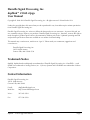
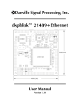
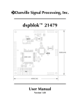
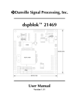
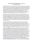
Danville Signal Processing, Inc. dspblok™ 21369+fpga CORE PS FLASH EEPROM SDRAM Analog Devices ADSP-21369 SHARC DSP 60.00 [2.36] Altera EP3C25/5 Cyclone III FPGA JTAG 60.00 [2.36] User Manual Version 1.01 Danville Signal Processing, Inc. dspblok™ 21369+fpga User Manual Copyright © 2009-2010 Danville Signal Processing, Inc. All rights reserved. Printed in the USA. Under the copyright laws, this manual may not be reproduced in any form without prior written permission from Danville Signal Processing, Inc. Danville Signal Processing, Inc. strives to deliver the best product to our customers. As part of this goal, we are constantly trying to improve our products. Danville Signal Processing, Inc., therefore, reserves the right to make changes to product specification or documentation without prior notice. Updated operating manuals and product specification sheets are available at our website for downloading. This manual may contain errors, omissions or “typo’s”. Please send your comments, suggestions and corrections to: Danville Signal Processing, Inc. 38570 100th Avenue Cannon Falls, MN 55009-5534 Trademark Notice dspblok, dspBootloader and dspstak are trademarks of Danville Signal Processing, Inc. VisualDSP++ and SHARC are trademarks of Analog Devices, Inc. Cyclone, Quartus and USB-Blaster are trademarks of Altera Corporation. Contact Information Danville Signal Processing, Inc. 38570 100th Avenue Cannon Falls, MN 55009 E-mail: Web Site: [email protected] http://www.danvillesignal.com Voice: 507-263-5854 Fax: 877-230-5629 dspblok™ 21369+fpga User Manual Page 1 Table of Contents Overview..................................................................................................................3 dspblok™ 21369+fpga ............................................................................................................................. 3 Intended Audience ...................................................................................................3 Getting Started..........................................................................................................4 Block Diagram ..........................................................................................................5 Programming the dspblok 21369+fpga.....................................................................6 dspBootloader .......................................................................................................................................... 6 Uploading Programs.................................................................................................................................. 6 User Modes .............................................................................................................................................. 7 Programming Modes ................................................................................................................................. 7 Uploading Procedure ................................................................................................................................ 8 Reading the Mode Pins ............................................................................................................................. 9 Hardware Overview ...............................................................................................10 Power Supply.......................................................................................................................................... 10 Memory.................................................................................................................................................. 11 DAI & DPI .............................................................................................................................................. 11 Data Bus ................................................................................................................................................. 11 Clocks..................................................................................................................................................... 12 Multiprocessor Configurations ................................................................................................................. 12 Reset....................................................................................................................................................... 12 Signal Levels ........................................................................................................................................... 12 Configuring the FPGA ............................................................................................................................. 13 Flash Management .................................................................................................................................. 13 Connections............................................................................................................................................ 14 Connector Recommendations & Notes ...................................................................16 Connector Specification .......................................................................................................................... 16 JH1 – JTAG (External ICE)........................................................................................................................ 16 JH2 – DAI, DPI, IO ................................................................................................................................. 16 JH3 – JTAG - AUX ................................................................................................................................... 16 JH4 – Power & Clock .............................................................................................................................. 16 JH5, JH6, JH7 – FPGA I/O....................................................................................................................... 17 JH8 – Boot and Clock Mode Configuration ............................................................................................. 18 Mechanical Dimensions..........................................................................................19 Schematic...............................................................................................................20 RoHS & WEEE Compliance.....................................................................................20 dspblok™ 21369+fpga User Manual Page 2 Overview Danville Signal's dspblok™ family of products delivers the power of digital signal processing in a small 60mm x 60mm form factor. Connections are brought out to standard 2mm dual row headers. The dspblok reduces development costs, risk and time. Danville’s dspblok DSP function modules are often incorporated directly into larger custom embedded systems. By taking advantage of pretested signal processing modules, pc board layouts become simpler and projects are completed quickly and cost effectively. You can also create small standalone embedded applications by combining a dspblok DSP function module with other dspblok modules. Embedded dspblok systems are created by using a dspblok power supply (such as our dspblok ps-usb), and an I/O module, such as one of our dspblok ad96k family of audio data converter boards. Each board is stacked via 2mm headers to create a low profile configuration where space is at a premium. dspblok™ 21369+fpga The dspblok™ 21369+fpga family are highly integrated DSP modules that incorporates an Analog Devices’ ADSP-21369 SHARC DSP operating at 400 MHz with an Altera Cyclone III FPGA. Flash, EEProm and SDRAM memory complement these devices. An onboard switching power supply supports the core voltage requirements of both the DSP and the FPGA so that only 3.3V is required to power the dspblok. The ADSP21369 peripherals include SPORTs (8), SPI(2), TWI (I2C), UART(2), timers, PWMs, JTAG and a full 32 bit wide data bus. These peripherals are available via 2mm headers on the dspblok. The FPGA of the dspblok™ 21369+fpga can extend peripheral support or can be used for signal processing functions. In addition to connections in common with the SHARC DSP, there are 70 uncommitted pins that are brought out to 2mm headers. The FPGA can communicate with the DSP through the DSP’s data bus as well as the DAI lines of the DSP. The dspblok 21369+fpga is the foundation of our dspstak™ 21369+fpga DSP Engines. You can use a dspstak 21369+fpga with ICE or a dspblok 21369+fpga with ICE as a development platform for the dspblok. The dspblok 21369+fpga family consists of the following standard modules: the dspblok™ 21369cy05, and the dspblok™ 21369cy25, based on Altera’s Cyclone III EP3C5 or EP3C25 FPGAs, respectively. Intended Audience The dspblok 21369+fpga requires an understanding of the Analog Devices’ ADSP-21369, as well as the Altera Cyclone III, and the associated tools used for development. If the dspblok 21369+fpga is going to be integrated into a larger hardware design, then it is also assumed that the user is familiar with basic hardware design. In most cases, systems integrators, DSP programmers and software engineers can create DSP embedded systems using our embedded dspblok systems (or dspstak family) without the need for additional hardware design and manufacturing. If you do not have a background with these skills, you may want to check out our web site dspblok™ 21369+fpga User Manual Page 3 (http://www.danvillesignal.com) as well as the Analog Devices and Altera web sites for links to useful references. Danville engineers are also available to discuss your application. Getting Started We strongly recommend that you use our dspstak 21369+fpga as an initial development platform. The dspstak 21369+fpga includes a dspblok 21369+fpga at its core. This dspstak card provides power and external interfacing connections. This combination gives you a solid footing for development before you incorporate the dspblok into your own target. The dspstak 21369+fpga w/ICE includes an on-board EZ-Kit style emulator that you can use for development and is supported by both the full version and kit version of Visual DSP++®5.0. The kit version is free. You can also use the dspstak as a dspblok programmer via its USB or UART ports. An alternative to this is to purchase a dspblok 21369+fpga w/ICE, which will allow you to do all of your development work on a pin compatible but elongated version of the dspblok 21369+fpga. This version has an Analog Devices ICE onboard and also has an Altera USB-Blaster, which allows for simultaneous debugging of both the DSP and the FPGA on the board. This approach does not offer the same production programming capabilities of the dspstak solution, however when using this setup it is possible to use the dspFlash which is also available from Danville Signal to program the dspblok 21369+fpga with both the DSP and FPGA code. You can also use a dspblok ps-usb power supply as part of a development system as well as a production programmer. The USB port allows you to upload your production firmware to the dspblok 21369+fpga DSP. In this case, we suggest you consider an Analog Devices HP USB emulator and an Altera USB-Blaster to facilitate your code development. The dspblok 21369+fpga includes the following items: Hardware: • dspblok 21369+fpga Module Documents (CD): • • • • This Manual CAD footprints (Gerber & Altium formats) Schematics Sample Programs We recommend that you have the documents: • • • • Analog Devices ADSP-2136x SHARC Processor Hardware Reference Manual Analog Devices ADSP-2136x SHARC Processor Programming Reference Manual Analog Devices ADSP-21160 SHARC DSP Instruction Set Reference Manual Altera Cyclone III Handbook We recommend that you have the following tools: • Analog Devices VisualDSP++ 5.0 for SHARC (available from Danville) dspblok™ 21369+fpga User Manual Page 4 • Quartus II 8.0 SP1, and optionally NIOS II EDS 8.0 • Analog Device HP USB ICE (available from Danville) • Altera USB blaster • Danville DSP+FPGA JTAG adapter or • Danville dspstak 21369+fpga with ICE • Analog Devices VisualDSP++ 5.0 for SHARC (optional, KIT license works with Danville ICE versions) • Altera Quartus II 8.0 • Altera NIOS II EDS 8.0 (Optional) and • dspFlash flash programmer for production programming (available from Danville) Our website (www.danvillesignal.com) has downloads and links to other tools and documents. Block Diagram LDO 2.5V FPGA PLL JH4 Switching Supply 3.3 V 3.3V JH2 DAI - 20 Pins JH2 DPI - 9 Pins JH2 SPI - Master 1.2V DSP Core FPGA Core 1.3V DAI [1..20] CLKOUT RESET# FLAGS DPI [4, 7..14] CTRL A[23..0] D[31..0] DPI [1..3] Serial Flash FPGA 1 (20 Pins) JH5 FPGA 2 (20 Pins) JH6 FPGA 3 (30 Pins) JH7 Configuration (PS from DSP) DPI [5] SDRAM DAI Connections (from DSP) SDRAM CTRL EEProm DPI [6] ADSP-21369, 400 MHz JH1, JH3 JH8 JTAG Altera Cyclone III EP3C5 -- EP3C25 JTAG JH1 DSP CONFIG dspblok™ 21369+fpga User Manual Page 5 Programming the dspblok 21369+fpga The dspblok 21369+fpga can be programmed in a variety of ways. In many cases, programs are uploaded via either a USB port or UART port into the on-board serial flash memory. This method relies on Danville’s dspBootloader™. The bootloader can load your SHARC application and the Cyclone III configuration file automatically at startup. Alternatively, you can use the SHARC’s internal bootloader to load your SHARC application and then manage the FPGA configuration from your DSP application. Both the DSP and FPGA code resides in the serial flash. You may program this flash via JTAG. Danville’s dspFlash Programmer can accomplish this task. During the development process, you can load and execute programs through the JTAG port by using either a built in debugger or an external emulator. The FPGA configuration file can also be debugged using an Altera USB-Blaster. dspBootloader The dspblok 21369+fpga has eight different programming modes that are assigned via jumper on the Configuration Header (JH8). The purpose of the programming modes is to establish what the dspblok 21369+fpga will do when it comes out of reset. Four of the programming modes are reserved for standard dspblok 21369+fpga functions and the remaining four are available for user programs. These modes are discussed in the following section. Mode 0 1 2 3 4 5 6 7 Boot State Silent (User config 0) Silent (User config 1) Silent (User config 2) Silent (User config 3) UART Only (Adjustable Baud) USB Only USB & UART (Adjustable Baud) USB & UART (115.2k Baud assuming 22.1184 MHz DSP ClkIn) Uploading Programs The dspblok 21369+fpga uses a 16Mbit SPI serial flash memory device to bootload the ADSP-21369. Assuming boot mode selection is set for SPI Master Boot (default), the ADSP-21369 will boot from the SPI flash memory after reset is deasserted. The dspblok 21369+fpga cannot fully utilize dspBootloader without an external USB or UART transceiver circuit. Danville offers several different boards, which provide this functionality, the dspblok ps-uart, the dspblok ps-usb, and the dspstak 21369+fpga are examples. If you would like to implement this functionality on your board, Danville engineers are available to discuss how to implement these interfaces. dspblok™ 21369+fpga User Manual Page 6 The internal boot capability in the ADSP-21369 is very useful except that there is no native support in the DSP to program the flash memory. The dspBootloader includes a flash writer program that addresses this problem. The other way to address this problem is the use the dspFlash to program the flash memory via JTAG. In the case of the dspblok 21369+fpga, dspBootloader also manages FPGA configuration. The dspblok 21369+fpga automatically boots dspBootloader. It is located in the lowest block of the flash memory. This program in turn, boots your program and the FPGA configuration file that resides in other sectors of the flash memory. You don’t have to worry about reserving memory for dspBootloader. In the process of loading your program, the bootloader program overwrites itself. User Modes Modes 0-3 are user definable modes. From the bootloader perspective, they are identical. In these modes, the bootloader will automatically load the DSP application code and then the application’s FPGA configuration file. These modes are “Silent” since they execute without any external communication or user intervention. User programs can read the Mode settings. For example, you could use Mode 0 as a means to execute one version of your application and use Mode 1 to execute another. Programming Modes Modes 4-7 are defined as programming modes. If the dspblok 21369+fpga is connected to an ASCII terminal and it is operating in a programming mode, you have a five second window to interrupt the boot process before the application program is automatically loaded. When you interrupt the boot process, the dspstak enters Command Mode. Command Mode lets you upload programs and FPGA configuration files to the flash memory. To support the USB communications, the FPGA is loaded with a temporary pass-through configuration that will allow the data bus of the DSP to connect to the USB interface. Without this configuration, USB communication is not possible. This configuration assigns 13 pins of the FPGA as D0-D7, A0, A1, MS2#, RD and WR. These pins are defined in the alternate assignment table in the Connector Section of this manual. The remaining user pins of the FPGA (57 of 70) are tri-stated in this situation. UART communication is available without the need to preconfigure the FPGA. If your application has contention issues, which would be created by the temporary FPGA configuration, you can use Mode 5, which only loads the application FPGA file (the FPGA is initially unconfigured). UART programming requires DPI 9 & 10. Mode 4 disables UART communication and therefore frees DPI 9 & DPI 10. Mode 6 and 7 are identical from a USB perspective. If the USB transceiver is enumerated, dspBootloader will start a dialog with an ASCII terminal via the USB port. the normal command modes. After exiting the command mode, the FPGA configuration is written to the FPGA and then the DSP application is loaded and executed. If USB is not enumerated, UART communication is assumed. The difference is that Mode 7 uses a fixed 115.2k baud (assuming a 22.1184 MHz DSP ClkIn), whereas Mode 6 can be set for other bauds. You write your DSP applications as normal and create a *.ldr file (Boot Type = SPI Slave, Format = Binary, Width = 8). If you want to upload your own FPGA configuration file, you need to create a *.rbf file using passive serial configuration. The *.rbf file should be compressed. dspblok™ 21369+fpga User Manual Page 7 When in command mode you can connect to the dspblok 21369+fpga using a terminal program. The baud rate for the UART is either 115200 (Mode 7) or 19200 (Mode 5,6). If you are using USB for uploading the baud rate is auto negotiated and the setting does not matter. Once you have the terminal open you can use the ? command to get help. User applications can write to unused flash memory, but be very careful that the dspBootloader program is never overwritten or erased. The only way to rewrite dspBootloader is with an emulator or dspFlash Programmer. It is very hard to damage the contents of the flash by accident, but it is possible. If you never write directly to the flash, you are unlikely to ever see a problem. Danville supplies sample code that manages the SPI bus where the flash memory resides. This code makes it even more difficult to write to the flash inadvertently. Uploading Procedure Command mode is available via USB or UART depending on the Mode setting. A USB device driver is included that emulates a COM port for Windows 2000, XP or Vista operating systems. Bootloader communications automatically switch between the UART port and the USB port. If the USB port is active (enumerated), the USB port is used; otherwise, the UART port will be active. Here are the basic steps to uploading programs: • Configure the dspstak 21369+fpga to operate in Mode 4,5,6 or 7. • Connect to an ASCII Terminal Program via UART or USB. USB is faster. o If UART communications is used, the serial configuration is 115.2K, N, 8, 1 for Mode 7 and 19.2K (default), N, 8, 1 for Mode 5 or 6. The baud can be reset to other bauds in Modes 5&6 using the B & C commands. Handshaking lines are ignored. Since many PCs no longer have an RS-232 port, you can also use an RS-232 to USB converter to emulate an RS-232 port. o If USB is used, the baud settings are ignored and the interface will operate like a very fast COM port. • Power Up or Reset the dspstak 21369+fpga. You should see a splash screen followed by moving # symbols. After about 5 seconds, the application program will boot unless you press a key to interrupt the boot process. This will bring a DSP> prompt signifying Command Mode. • Type ? to view a list of available commands. • Type U to upload a new DSP program file. Your program must be a *.ldr (ADI loader file) with the following parameters: o o o Boot Type = SPI Slave Format = Binary Width = 8 After you confirm the upload, the bootloader will erase the affected flash memory space. At the dspblok™ 21369+fpga User Manual Page 8 Ready: prompt, use your ASCII terminal program to send the .ldr file. Make sure you enable the "binary transfer" option. You may also use the UA command to upload a similar file in ASCII format. This will take longer. In Tera Term Pro, choose "Send File..." from the "File" menu. Click the "Binary" checkbox, and then open your .ldr file. As the file transfers, you will see one progress mark for every 128 bytes transferred. Data transfer must be continuous. If the host stops sending data for more than approximately 500ms, the bootloader will assume that the code upload is complete and terminate the transfer. • After the program is uploaded, a checksum is calculated and you have the opportunity to enter a description of the program. The program description is an ASCII string that you can use to identify your program. It does not impact the function of the DSP module in any way, but can be a helpful way to track program revisions. A typical program description might be "Filter version 1.00.” The size of the program is also calculated. • Type UF to upload a new FPGA configuration file. Your program must be a *.rbf (Altera raw binary file). The procedure is the same as the U command. • Type Q to quit Command Mode and the application program will boot. There are a number of additional commands that are available in Command Mode. For example, you can read, write and erase EE memory form the DSP> prompt. There is no option to read back the application program via the Command Mode. This is to help you keep your code a little more proprietary. We suggest that you use the checksum information as a check during production programming to insure that your program was loaded correctly. Reading the Mode Pins The mode pins can be read by the DSP directly. This can by done by executing the following procedure. 1) Lower the FPGA SS, which is part of the multiplexed flag 0 and flag 1. This is state 00 2) Write 0x00, then 0xFF which will create the required low to high transition that is required by the Cyclone III, this enables the 74CBTLV3245 buffer which grants the Data bus access to the configuration pins. 3) Read the state of the mode pins on D0, D1, D2 4) If you have not done so already raise FPGA SS. dspblok™ 21369+fpga User Manual Page 9 Hardware Overview The dspblok 21369+fpga is a small module measuring 60mm x 60mm (2.36” x 2.36”). JH2- JH7 are 2mm male headers that are installed on the bottom side of the pc assembly. JH1 and JH8 are mounted on the top side of the pc assembly. If mating 2mm female headers (4.3mm ht.) are used, the pc assembly will be about ¼” above the mating pc board. This allows standard sized standoffs to be used with the corner mounting holes if desired. The hole size is 2.3mm (0.090”) – suitable for 2-56 screws. JH8 JH4 CORE PS FLASH EEPROM SDRAM Analog Devices ADSP-21369 SHARC DSP JH1 – JTAG (connects to external ICE) • JH2 – DAI, DPI, I/O, SPI & System • JH3 – JTAG (dspstak connection) • JH4 – Power & Ext Clock • JH5, JH6, JH7 – FPGA I/O or Data bus with FPGA operating as a pass through • JH8 – Clock & Boot Configuration 60.00 [2.36] JH2 JH5 JH6 Altera EP3C25/5 Cyclone III FPGA JH3 • JTAG JH1 JH7 60.00 [2.36] Power Supply There are two power supply connections to the dspblok: Core (Vdd) and I/O (Vd+3.3). The DSP and FPGA core supplies may range from 3.3V to 5V. This is the input to an on-board switching power supply that supplies 1.3V to the ADSP-21369 and 1.2V to the Cyclone III FPGA. DO NOT use a higher voltage supply for the core supply input (JH4-Vdd). A single 3.3V supply is all that is required to power the dspblok 21369+fpga. A 5V supply will be slightly more efficient but a 3.3V supply may be more convenient. The DSP I/O and Memory supply must be 3.3V. For example, the dspstak 21369+fpga uses a 3.3V supply to feed the DSP core and the dspblok Vd+3.3 (I/O). On this product, the 3.3V is created by a switching supply that converts directly to 3.3V. Alternatively, a product uses a 5V supply to feed the DSP core (Vdd) and other external 5V I/O devices and also drives a 3.3V LDO. The 3.3V output from the LDO drives the dspblok Vd+3.3 (I/O) and other external 3.3V devices. In this case, it makes no sense to power the dspblok core with 3.3V since the LDO would be dissipating the excess voltage as heat. The dspblok 21369+fpga requires a single 3.3V supply to operate. An on-board switching supply eliminates the need for an external core supply. This switching supply operates well with a 3.3V input but also accepts 5V as an option. Power consumption is largely a function of the operating clock of the ADSP-21369 and the computation tasks that are being executed on the DSP. The highest consumption occurs when the DSP is performing continuous floating point operations at maximum core clock (400MHz). Accessing external I/O such as the dspblok™ 21369+fpga User Manual Page 10 SDRAM or other peripherals consumes less power in the benchmarks that we have performed. FPGA power consumption will vary considerably depending on the dynamic execution of the device. Memory The ADSP-21369 includes an on board SDRAM controller. External SDRAM allows 32 bit wide data to be accessed by the DSP. The ADSP-21369 does not support program execution or extended precision data from the SDRAM. On the dspblok 21369+fpga, #MS0 is assigned to support the 4Mx32 (128Mbit) SDRAM. A 16Mbit serial flash memory may be used to bootload the DSP and the FPGA. There is a pre-installed bootloader program that resides in the flash. This program accepts standard ADI loader files (SPI, slave, binary, 8 bit) as well as FPGA programming (rbf) files. Files can be uploaded with either a dspblok ps-usb power supply or a dspstak 21369+fpga. The last 14 blocks of the flash is reserved for application memory. You can read and write this block from your DSP application. If you want to manage the flash memory yourself, you can overwrite the internal bootloader via the JTAG port. 64kbits of EEProm memory is also available as byte addressable user memory. For example, you might store serial numbers, build versions or calibration values in this space. It is also possible to replace this EEProm with flash if your application requires up to 16 Mbit more flash. Consult Danville if you application will require additional flash memory DAI & DPI The ADSP-21369 has 20 DAI lines and 14 DPI lines. Collectively these can be thought of as two sets of crossbar switches that connect to a wealth of peripherals. The dspblok 21369+fpga maintains the flexibility of the DAI and DPI by bringing out all 20 DAI and 12 of 14 DPI lines to external connections. The DAI is completely unencumbered and can be assigned to I/O in an arbitrary manner. The DPI is slightly restricted in that the primary SPI interface is assigned to DPI1 (MOSI), DPI2 (MISO), DPI3 (SCK), DPI5 (Flash SS) and DPI6 (EE SS). With the exception of DPI6, these connections are necessary to support SPI master booting. The dspblok 21369+fpga may also be booted from an external host using SPI slave mode. In this case DPI4 is also used as the #SPIDS line. The FPGA also has access to the DAI lines. This allows the FPGA to have access to the same devices as the DSP. You can also use these connections for interprocessor (DSP&FPGA) communications. Data Bus The data bus of the DSP can be accessed through the FPGA. This means that to access the data bus at the connectors the FPGA needs to be configured properly. The Danville boot loader always loads a full data bus pass through configuration into the FPGA so that USB communication on the PS-USB power supply and communication with the dspstak baseboard are possible. The schematic and HDL code of this pass through application are provided on the CD. The FPGA can have up to 70 available pins that are connected to JH5, JH6, and JH7. These serve as the dspblok™ 21369+fpga User Manual Page 11 data bus and control lines of the dspblok 21369zx. Any or all of the DSP data bus can be passed through the FPGA depending on the requirements of your system. Clocks The dspblok 21369+fpga supports both internal and external clocking options. You can add a standard HC49 style crystal to the board for internal clocking or you can supply an external clock. The configuration header (JH8) allows any ADSP-21369 power-up clock configuration to be set. The DSP provides the clock for the FPGA with its CLKOUT pin. This means that the end user will have to ensure that the CLKOUT is enabled to use the FPGA or JH5-7. Multiprocessor Configurations The dspblok 21369+fpga may be used as a coprocessor in a larger system. Perhaps the easiest way to communicate with an external host to configure the secondary SPI port as a slave. The primary SPI port remains configured as an SPI master so that it can manage local resources such as flash and EE memory as well as other I/O devices. You can also use SPORTs for interprocessor communication. This can be a good approach in multiple DSP processor applications. For example, you might use several dspbloks to provide front end signal processing for a multichannel application. The results could be routed to a dspstak that manages the whole system and communicates to the outside world. A third option is to use the FPGA, especially if the other processor is another dspblok+fpga. This could be done using any combinations of the available pins and virtually any communication protocol you can implement on the FPGA. Other options are possible; these include UART and I2C, which can be used with the DSP alone. The other options are to utilize the FPGA. This can enable communication using the DSP data bus, which requires the FPGA to be configured as a pass through. The other options would be to configure the FPGA with a different peripheral, which could be as simple as SPI or as complex as Ethernet and relay the information to the DSP using the data bus. Reset The dspblok 21369+fpga automatically resets when the 3.3V power supply is stable. #RESET is active low and open drain. This means that an external device(s) may also reset the dspblok by pulling the reset line low. External devices should not drive #RESET high since this can cause contention with the on-board reset circuit. The external reset circuit is connected in a wired-OR configuration using an active low – open drain configuration. A 74LVC125 or an open collector/drain transistor circuit are possibilities. You do not need an additional pull up resistor. Signal Levels The dspblok 21369+fpga uses standard 3.3V logic levels. These levels have become the defacto operating standard for many years now. DO NOT use 5V logic when interfacing to the dspblok. The inputs are not 5V tolerant. Most external devices requiring 5V TTL levels can be safely driven by the dspblok. If you have dspblok™ 21369+fpga User Manual Page 12 questions concerning interfacing external devices, please contact Danville for suggestions. Configuring the FPGA The Danville bootloader will configure the FPGA during boot time to pass through the data bus, which makes it possible to utilize USB with the dspstak 21369+fpga or the ps-usb power supply. The Danville bootloader is capable of loading user code into the FPGA before booting the DSP. This code can be uploaded as an rbf file and written into flash by the bootloader. If you would like to configure the FPGA from your DSP application, the source is available on the CD. This function will read an rbf file from flash and configure the FPGA as outlined below. The FPGA on the dspblok 21369+fpga is configured by the DSP using the passive serial format. This configuration makes use of the DSP’s data bus, which can be set as flags. The interface consists of D3 (nStatus), D4 (nConfig), D5 (Conf_Done), D6 (DCLK) and D7 (Data0). Procedure for configuring the FPGA: 5) Lower the FPGA SS, which is part of the multiplexed flag 0 and flag 1. This is state 00 6) Write 0x00, then 0xFF which will create the required low to high transition that is required by the Cyclone III, this enables the 74CBTLV3245 buffer which grants the Data bus access to the configuration pins. 7) Execute the configuration sequence as described in the Cyclone III handbook (available in pdf form www.altera.com). 8) After the configuration is finished and the Conf_Done pin has been raised, Lower the FPGA SS again and write 0xFF which will disable the 74CBTLV3245 buffer and allow the data bus to resume its normal functions. Flash Management The Danville bootloader uses one possible flash management scheme. The way the flash is partitioned utilizes the natural sector format because it is only possible to erase using these boundaries. This allows space for the boot loader, the boot FPGA configuration, the user FPGA configuration, the user DSP code, and the user memory space. These sections occupy the 16 Mbit onboard serial flash. If you upload your user code using the Danville bootloader your code will automatically be put into the correct partition, however if you do not want to use the bootloader and would like to program the flash using a device similar to the dspFlash, here are the important things to consider. The FPGA configuration files are often quite large. A compressed rbf file for the dspblok 21369cy25 can be up to 6 Mbit. This size means the 16Mbit flash is capable of holding 2 FPGA configurations. The FPGA code flash location(s) need to be known by the DSP in order to configure the FPGA properly. The DSP boot code needs to be located at address 0, the other pieces of code need to be located far enough away so they do not intersect with the DSP code. dspblok™ 21369+fpga User Manual Page 13 Connections Pin JH1 Note 1 Description JTAG 1 2 3 4 5 6 7 8 9 10 11 12 13 14 15 16 FPGA TCK FPGA TDI FPGA TDO GND FPGA TMS DSP TMS GND DSP TCK DSP EMU DSP #TRST DSP EMUSEL DSP TDI KEY (no pin) DSP TDO Vd+3.3 Vd+3.3 dspblok™ 21369+fpga User Manual Pin JH2 Note 2 Description DAI, DPI, IO 1 2 3 4 5 6 7 8 9 10 11 12 13 14 15 16 17 18 19 20 21 22 23 24 25 26 27 28 29 30 31 32 33 34 35 36 37 38 39 40 GND DPI8/IO0/#SS1 DPI4/IO1/#SS2 DPI13/IO2/#SS3 DPI14/IO3/#SS4 FLG0/IO4/#SS5 DPI7/#SS0 DPI11/I2C_SDA DPI12/I2C_SCL DPI9/UART_TX DPI10/UART_RX FLG1 GND DPI1/MOSI DPI3/SCK DPI2/MISO #RESET GND DAI1 DAI2 DAI3 DAI4 DAI5 DAI6 DAI7 DAI8 DAI9 DAI10 DAI11 DAI12 DAI13 DAI14 DAI15 DAI16 DAI17 DAI18 DAI19 DAI20 GND GND Pin JH3 Note 3 Note 3 JTAG - AUX 1 2 3 4 5 6 7 8 9 10 JH4 Note 4 Note 5 Note 5 Description GND EMUSEL EMU TDO TDI #TRST TCK TMS Factory Factory Power 1 2 3 4 5 6 7 8 9 10 GND Ext Clk Vd+1.3 DSP ClkOut Vd+3.3 Vd+3.3 Vdd (3.3V or 5V) Vdd (3.3V or 5V) SYNC GND Page 14 Pin JH5 Data Bus 1 2 3 4 5 6 7 8 9 10 11 12 13 14 15 16 17 18 19 20 JH8 Note 7 Note 7 Note 8 Note 8 Description FPGA I/O E8 FPGA I/O F8 FPGA I/O E6 FPGA I/O D5 FPGA I/O D6 FPGA I/O C6 FPGA I/O E7 FPGA I/O E9 FPGA I/O C8 FPGA I/O D8 FPGA I/O B11 FPGA I/O A11 FPGA I/O C9 FPGA I/O D9 FPGA I/O E10 FPGA I/O C11 FPGA I/O D12 FPGA I/O D11 FPGA I/O F9 FPGA I/O E11 Pin JH6 Description Data Bus 1 2 3 4 5 6 7 8 9 10 11 12 13 14 15 16 17 18 19 20 FPGA I/O A2 FPGA I/O A3 FPGA I/O B4 FPGA I/O A4 FPGA I/O B5 FPGA I/O A5 FPGA I/O B6 FPGA I/O A6 FPGA I/O B7 FPGA I/O A7 FPGA I/O B10 FPGA I/O A10 FPGA I/O B12 FPGA I/O A12 FPGA I/O B13 FPGA I/O A13 FPGA I/O A14 FPGA I/O B14 FPGA I/O B16 FPGA I/O A15 Boot & Clk 1 2 3 4 5 6 7 8 9 10 11 12 13 14 15 16 BOOTCFG0 GND BOOTCFG1 Vd+3.3 CLKCFG0 Vd+3.3 CLKCFG1 Vd+3.3 Vd+3.3 #RESET GND MODE 0 GND MODE 1 GND MODE 2 Pin JH7 Description Data Bus 1 2 3 4 5 6 7 8 9 10 11 12 13 14 15 16 17 18 19 20 21 22 23 24 25 26 27 28 29 30 FPGA I/O N14 FPGA I/O P15 FPGA I/O L13 FPGA I/O L14 FPGA I/O J14 FPGA I/O J13 FPGA I/O D16 FPGA I/O R16 FPGA I/O N15 FPGA I/O P16 FPGA I/O N16 FPGA I/O L15 FPGA I/O K15 FPGA I/O L16 FPGA I/O K16 FPGA I/O J15 FPGA I/O H15 FPGA I/O J16 FPGA I/O H16 FPGA I/O G15 FPGA I/O F15 FPGA I/O G16 FPGA I/O F16 FPGA I/O C15 FPGA I/O D15 FPGA I/O C16 FPGA I/O F14 FPGA I/O C14 FPGA I/O F13 FPGA I/O D14 Note 1: Mating Plug is plugged to prevent misalignment. Note 2: DPI4 also functions as #SPIDS in SPI slave booting applications. Note 3: Leave Unconnected. dspblok™ 21369+fpga User Manual Page 15 Note 4: Vd+1.3 is for power supply monitor only (DSP Core supply). Note 5: Vdd is externally supplied: 3.3 to 5V (Vin for DSP Core Switching supply). Both connections must be the same voltage. Note 7: Boot Configuration is 01 by default (SPI Master Booting). Note 8: Clock Configuration is 00 by default (6 x ClkIn), generally reconfigured in program code. Connector Recommendations & Notes Connector Specification All dspblok connectors are gold plated 2mm dual row headers. Male connectors are either soldered on the dspblok pc assembly or supplied for optional assembly by the customer. Mating female connectors are included for your target pc board. The plastic base of each male connector is 2mm. The height of the female headers is 4.3mm. This means that the inserted combined height of the two connectors is 6.3mm or approximately ¼ inch. Standard standoffs may be used to secure the dspblok to the target pc board. Mounting holes are 2.3mm (0.090 inch) dia. to accommodate a 2-56 screws or standoffs. JH1 – JTAG (External ICE) This connector is mounted on the top side of the dspblok. A 2mm right angle header is used instead of the larger ADI JTAG header. The connections on the JTAG header correspond with the connections on an ADI JTAG header, as well as, an Altera JTAG header. In addition, Vd+3.3 is also available. This addition allows an active buffer circuit to be added for JTAG chaining applications. Danville has a dual JTAG adapter available (P/N A.08154) that allows for simultaneously debugging the DSP and FPGA with the appropriate emulation hardware. JH2 – DAI, DPI, IO This connector is mounted on the bottom side of the dspblok. The DAI lines are all uncommitted by the dspblok. With the exception of the SPI lines, the DPI can be freely assigned. The alternate names in the table are dspstak I/O conventions. If you are using a dspstak for development, it may be prudent to following these usage conventions. JH3 – JTAG - AUX This connector is mounted on the bottom side of the dspblok. It is used to allow a mating board such as a dspstak access to the JTAG port. JH4 – Power & Clock This connector is mounted on the bottom side of the dspblok. This is the main power feed to the dspblok, Vdd is the input to the core switching supply. Both Vdd pins should be connected to together and fed with either 5V or 3.3V. Likewise, Vd+3.3 should be connected together and fed with 3.3V. Vd+1.3 is current limited by a large resistor. Its purpose is for diagnostics. dspblok™ 21369+fpga User Manual Page 16 JH5, JH6, JH7 – FPGA I/O Uncommitted FPGA I/O is available on JH5, JH6, and JH7. There are 70 pins, located in I/O banks 5, 6, 7 and 8, which can be safely used by your FPGA configuration. In some situations, the DSP data bus (or a portion thereof) needs to be assigned to these pins. For example, the dspBootloader requires a portion of the data bus to support USB booting. Danville supplies source files (HDL & Schematic) to include in your FPGA design to facilitate this task. Pin JH5 Note 2 Note 2 Note 2 Note 2 Note 2 Note 2 Note 2 Note 2 Note 1 Note 1 Note 1 Note 1 Note 1 Note 1 Note 1 Note 1 Note 1 Note 1 Description Data Bus 1 2 3 4 5 6 7 8 9 10 11 12 13 14 15 16 17 18 19 20 D15 D14 D13 D12 D11 D10 D9 D8 D7 D6 D5 D4 D3 D2 D1 D0 #RD #WR ACK Available Pin JH6 Description Data Bus 1 2 3 4 5 6 7 8 9 10 11 12 13 14 15 16 17 18 19 20 Pin JH7 D31 D30 D29 D28 D27 D26 D25 D24 D23 D22 D21 D20 D19 D18 D17 D16 Available Available Available Available Note 1 Note 1 Note 2 Note 1 Description Data Bus 1 2 3 4 5 6 7 8 9 10 11 12 13 14 15 16 17 18 19 20 21 22 23 24 25 26 27 28 29 30 Available Available Available A23 A22 A21 A20 A19 A18 A17 A16 A15 A14 A13 A12 A11 A10 A9 A8 A7 A6 A5 A4 A3 A2 A1 A0 #MS1 #MS2 #MS3 Note 1: Necessary for USB communications using dspBootloader and dspstak zx compatibility. Note 2: Necessary for dspstak zx2 compatibility in addition to pins from Note 1. dspblok™ 21369+fpga User Manual Page 17 JH8 – Boot and Clock Mode Configuration JH8 is not normally installed. Both the clock and boot configuration pins are pulled passively to configure the boot mode to [01], SPI Master Mode and clock mode to [00], 6:1 Core/Clkin. The reason that JH8 is not installed is that there are several possibilities for using these connections. Case 1: Do nothing. Most dspblok 21369+fpga applications are best served by using the defaults. This does not mean that the core clock must be restricted to 6 x ClkIn. The more flexible method is to reprogram the core clock in software at the beginning of the application program. This gives the application substantially more flexibility than the three choices presented by ClkCfg. Case 2: Mount a male header on the top side of the pc board. This allows a jumper to be placed across the header to change the state of the pin. Case 3: Mount a male header on the bottom side of the pc board. This allows the connections to be routed to a mating pc board. Perhaps the best reason for using this configuration would be for systems that normally used the on-board flash for SPI Master booting, but also could use an external host for SPI Slave booting. The host processor can control #RESET so that the configuration can be switched by the host. #RESET is also duplicated on JH8. This might be a convenient place for an external reset circuit or switch. If you use a push button switch, we suggest using a 1K series resistor and a 3K3 pullup resistor. This will help protect the circuit from static electricity (from your finger and the carpet in your office). dspblok™ 21369+fpga User Manual Page 18 Mechanical Dimensions 46.00[1.81] 6.00 [0.24] C7 D1 C13 U12 C12 C19 U7 8 7 6 5 1 2 3 4 8 7 6 5 U9 1 2 3 4 Top Side U8 L2 U11 L1 U6 U1 60.00[2.36] U3 44.00[1.73] U10 U5 Y1 U2 24.00 [0.95] U4 9.00 [0.35] JH1 6.00 [0.24] 26.00 [1.02] 52.00 [2.05] 57.00[2.25] 60.00[2.36] Holes 2.3 [0.090] (4 places) JH4 Bottom Side 55.00[2.17] JH2 JH6 JH5 JH3 JH7 55.00 [2.17] Mounting holes are equidistant from the center of the dspblok. These holes are 0.090 in diameter, suitable for 2-56 screws. When 4.3mm height mating female connectors are used, the board will be 6.3mm (0.25 in) above the target board, therefore 0.250 standoffs may be used. Component height above the board is 6mm (0.236 in). The board is .062 in thick. dspblok™ 21369+fpga User Manual Page 19 Schematic The Distribution CD includes schematic diagrams of the dspblok 21369+fpga. RoHS & WEEE Compliance The European Union approved a directive on the restriction of the use of certain hazardous substances in electrical and electronic equipment. This directive is commonly known as RoHS, EU Directive 2002/95/EC. This directive severely limits the amount of lead and 5 other substances that can be in contained in nonexempt products. The directive became European law in February 2003 and took effect July 1, 2006. It is likely that other countries outside the European Union and some states in the United States may adopt similar legislation. There are a number of important exemptions that affect many of our customers. The most important of these is Category 9, Control and Monitoring Instruments. You may wish to review your situation to see if this exemption applies to you. Military, medical and some other products are also exempt. We suggest that you make an appropriate assessment concerning your products. The dspblok 21369+fpga is RoHS compliant. The dspblok 21369+fpga is a subcomponent of a larger system; therefore it is not subject to the WEEE directive EU Directive 2002/96/EC. dspblok™ 21369+fpga User Manual Page 20