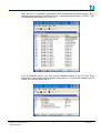
1
Maxiflex P3 CPU’s
M126xD
User’s Manual
Date
Revision
Comments
March 2003
March 2003
April 2003
April 2003
April 2003
April 2003
May 2003
1
2
3
4
5
6
7
April 2004
8
Sept 2004
9
Initial Issue
Ethernet configuration updated
Minor Corrections
Ethernet Addressing updated
Battery Link information added
Typographical corrections
DITcopy Function Block updated and Network DIP Switch
not active on A versions of the product.
Added Subscriptions, Modbus Master and ISaGRAF
programming extension. Model ‘D’.
Added more Content for Modbus Master. Added new DIT
access function blocks to ISaGRAF programming
extensions.
SOFTWARE COPY AVAILABLE
This manual is available in printed form or in Adobe Acrobat pdf format.
The pdf file is named UMM126XDR09.pdf
COPYRIGHT AND PROTECTIVE NOTICES
1.
The Copyright of this document and the associated drawings, is the property of Omniflex and
is issued on condition that it is not copied, reprinted or reproduced or transmitted in any form or by any
means, electronically, photocopying, mechanical or otherwise, nor its contents disclosed, either wholly
or in part, without the consent in writing of, or in accordance with the conditions of a contract with
Omniflex.
2.
The publication of information in the document does not imply freedom from patent or other
protective rights of Omniflex or others.
3.
Although every intention is made to ensure that performance figures and data are accurate the
company reserves the right to alter without notice any product or specification. Performance figures
and data must therefore be specifically confirmed by the company before they become applicable to
any tender, order or contract.
4.
In the case of electrical components, enough data is included in the drawings to allow
maintenance of the equipment. However, if component availability or substitution information is
required please consult the factory for assistance, as it is impossible to include data on every
component in this document.
5.
This product is sold without liability for consequential loss of any description.
Maxiflex P3 CPU User Manual
UMM126XDR09.pdf
2
-© Omniflex
SCOPE
This User Manual provides information on how to install, configure and use the Maxiflex P3 CPU.
Programming features specific to these products are included in this manual.
This manual does not cover the fundamentals of the IEC61131-3 programming languages, or the
Omniflex ISaGRAF Programmer’s Workbench. This information is available in the manuals for this
product.
This manual covers the following product Models:
Model
Description
M1260D
M1261D
P3 CPU with RS232/485 Serial Port
P3c CPU with RS232/485 Serial Port and Conet/c
Twisted Pair Network Port.
P3e CPU with RS232/485 Serial Port and Conet/e
Ethernet Network Port.
M1262D
Introduction
The MAXIFLEX P3 range of CPU’s is designed for general industrial control applications including
process control, PLC, telemetry and remote I/O applications. These CPU’s combine powerful
industrial network communications capabilities with ease of use and powerful programming
features.
All I/O and configuration data variables are automatically accessible through up to 65,000 Data
Interchange Registers in a single virtual “Data Interchange Table”, allowing the implementation of
Remote I/O systems “out of the box”.
Conventional remote I/O systems can be implemented without the need for any programming,
although the inclusion of programming capability in the P3 with the versatile IEC61131
programming languages allows sophisticated local control functions to be performed.
Many other features such as a built-in real-time clock, battery backup for temporary dynamic data,
and a MODBUS (Master or Slave) or Conet/s equipped RS232/485 serial port are standard in
these products.
Powerful features such as automatic I/O module recognition and scanning, remote programming,
and a versatile Remote Data Subscription Service, all contribute to making the P3 CPU a “plugand-work” product that dramatically reduces system engineering time.
Maxiflex P3 CPU User Manual
UMM126XDR09.pdf
3
-© Omniflex
Table of Contents
1. GENERAL DESCRIPTION ....................................................................................................... 9
1.1 Front Panel LED Indicators: ................................................................................................... 9
1.2 Serial Port: (applicable to all P3 CPUs)................................................................................ 10
1.3 Programming Port: (applicable to all P3 CPUs) ................................................................... 10
1.4 Conet/c Network Port: (only applicable to M1261D P3c CPU)............................................. 10
1.5 Conet/e Network Port: (only applicable to M1262D P3e CPU) ............................................ 11
1.6 I/O Module support ............................................................................................................... 11
2. Installing the P3 CPU ............................................................................................................ 12
2.1 Connecting the Internal Battery ............................................................................................ 12
2.2 Connecting the memory battery backup............................................................................... 12
2.3 Installing the P3 CPU on the Maxiflex base ......................................................................... 12
2.4 Connecting the Programming port (all models).................................................................... 13
2.5 Connecting the Serial port (all models) ................................................................................ 13
2.6 Connecting the Conet/c network port (M1261D P3c CPU only)........................................... 14
2.7 Connecting the Conet/e network port (M1262D P3e CPU only) .......................................... 14
2.8 Connecting the Watchdog Relay Output Contact................................................................. 14
2.9 Applying power for the first time ........................................................................................... 14
2.10
Front-Panel LED Indicators Explained .......................................................................... 14
2.10.1 CPU OK ....................................................................................................................... 14
2.10.2 I/O OK .......................................................................................................................... 15
2.10.3 RUN ............................................................................................................................. 15
2.10.4 BATT ............................................................................................................................ 15
3. P3 CPU’s and the MAXIFLEX Architecture......................................................................... 16
3.1 System Architecture ............................................................................................................. 16
3.1.1 Data Interchange Table (DIT) Overview ........................................................................ 16
3.1.2 Intelligent Modules explained......................................................................................... 16
3.1.3 I/O Modules explained ................................................................................................... 16
3.2 CPU Functions...................................................................................................................... 17
3.2.1 Real-Time Clock............................................................................................................. 17
3.2.2 I/O Scanning .................................................................................................................. 17
3.2.3 I/O Module Management ............................................................................................... 17
3.2.4 Subscription Service ...................................................................................................... 17
3.2.5 Conet Routing Service ................................................................................................... 17
3.2.6 IEC61131 User Program................................................................................................ 18
4. Configuring a P3 CPU........................................................................................................... 20
4.1 Programming the P3 CPU .................................................................................................... 20
4.2 Preparing OMNISET or DITview to configure the P3 CPU .................................................. 20
4.2.1 OMNISET....................................................................................................................... 20
Maxiflex P3 CPU User Manual
UMM126XDR09.pdf
4
-© Omniflex
4.2.2 DITview .......................................................................................................................... 20
4.2.3 Connecting OMNISET to the CPU................................................................................. 20
4.3 Configuring the Programming Port ....................................................................................... 21
4.4 Configuring the Real-time Clock........................................................................................... 21
4.5 Configuring the Serial Port ................................................................................................... 22
4.5.1 MODBUS Slave Protocol ............................................................................................... 23
4.5.1.1. Default MODBUS Mode - ASCII Slave at 9600 baud ............................................ 23
4.5.1.2. Standard MODBUS Slave Protocol Mode ............................................................. 23
4.5.1.3. Modbus Data Register Mapping............................................................................. 24
4.5.2 MODBUS Master Protocol ............................................................................................. 25
4.5.2.1. Standard MODBUS Master Protocol Mode ........................................................... 25
4.5.3 Conet/s (Peer-to-peer) Protocol..................................................................................... 26
4.5.3.1. Default Conet/s Mode (19200 baud)...................................................................... 26
4.5.3.2. Standard Conet/s Protocol Mode ........................................................................... 26
4.6 Configuring the Conet/c Network Port (available on the M1261D P3c CPU only.) .............. 26
4.7 Configuring the Ethernet Network Port (available on the M1262D P3e CPU only.)............. 27
4.7.1 Protocols supported simultaneously .............................................................................. 27
4.7.2 Assigning an IP Address ................................................................................................ 27
4.7.3 Assigning a Node Address............................................................................................. 28
5. The Data Interchange Table explained ............................................................................... 29
5.1 DIT Table Layout .................................................................................................................. 29
5.2 CPU Dynamic Data Space (0-29,999).................................................................................. 30
5.3 Intelligent Modules in I/O Slots 1 to 15 (30,000-59,999) ...................................................... 30
5.4 CPU Configuration (Static) Data Space (60,000-65,499)..................................................... 31
5.5 DIT Access to I/O Modules in I/O Slots 1 to 15 .................................................................... 31
6. I/O Module Management & Scanning Explained................................................................ 33
6.1 The I/O Module Manifest ...................................................................................................... 33
6.1.1 Configuring an I/O Manifest using Omniset ................................................................... 33
6.1.1.1. Automatic Manifest Configuration .......................................................................... 33
6.1.1.2. Manual Manifest Configuration .............................................................................. 33
6.1.2 Checking the Status of installed modules ...................................................................... 34
6.1.3 Front-Panel I/O Status Indication................................................................................... 36
6.2 Automatic I/O Scanning........................................................................................................ 36
7. The Subscription Service Explained................................................................................... 37
7.1 Introduction to Subscriptions ................................................................................................ 37
7.2 Setting up subscriptions ....................................................................................................... 37
7.3 Number of subscriptions allowed.......................................................................................... 39
7.4 Subscription Application Example ........................................................................................ 39
8. Modbus Master Operation Explained.................................................................................. 41
8.1 Introduction to Modbus Master Driver .................................................................................. 41
Maxiflex P3 CPU User Manual
UMM126XDR09.pdf
5
-© Omniflex
8.2 Modbus Master Parameters ................................................................................................. 41
8.3 Query Configuration ............................................................................................................. 43
8.4 Query Triggers...................................................................................................................... 44
8.5 Status DIT Registers ............................................................................................................ 45
9. I/O Module DIT Register Reference ..................................................................................... 46
9.1 M1101A –24VDC/12V Solar 3A Charger/Power Supply ...................................................... 46
9.2 M1102A – DC L - 24Vdc Logic Power Supply...................................................................... 46
9.3 M1104A – DC LF - 48Vdc Logic/Field Power Supply........................................................... 46
9.4 M1151B – AC LF - 115/230Vac Logic/Field Power Supply.................................................. 47
9.5 M1152B – AC LC - 115/230Vac Logic Power Supply/Charger. ........................................... 47
9.6 M1321A – 8DI-C - 8 way Individually Isolated Contact Input Module .................................. 47
9.7 M1322A - 16DI - 16 way Digital Input Module (9-30Vdc) M1323A - 16DI - 16 way Digital
Input Module (18-60Vdc) ............................................................................................................. 48
9.8 M1326A – 32DI – 32 way Digital Input Module .................................................................... 48
9.9 M1330A – 8DI8RO 8way Digital Input /8 way Relay Output Module ................................... 49
9.10
M1341B – 16DO – 16way Digital Output Module ......................................................... 49
9.11
M1342A – 32DO – 32way Digital Output Module ......................................................... 50
9.12
M1372A – 8RO – 8way Relay Output Module .............................................................. 50
9.13
M1403A – 16AI – 16way Analogue Input Module ......................................................... 51
9.14
M1412A – 8AO – 8 way Analogue Output Module ....................................................... 51
9.15
M1431B – 8VC ISO – 8 way Isolated Voltage/Current Input Module ........................... 52
9.16
M1432B – 8TC ISO – 8 way Isolated Thermocouple/milliVolt Input Module ................ 55
9.17
M1433B – 6RTD ISO – 6 way Isolated Resistance Bulb Input Module ........................ 58
10. Programming the P3 CPU .................................................................................................... 61
10.1
Introduction to IEC61131-3 Programming..................................................................... 61
10.1.1 The IEC61131 Standard .............................................................................................. 61
10.1.2 The IEC61131-3 Programming Languages ................................................................. 61
10.2
Programming the Maxiflex P3 CPU............................................................................... 62
10.3
Installing the Application Workbench for the Maxiflex P3 CPU..................................... 62
10.4
Setting up the Application Workbench for the Maxiflex P3 CPU................................... 63
10.4.1 PC-PLC Link Parameters............................................................................................. 63
10.4.2 I/O Slot and Channel Numbering ................................................................................. 64
10.4.3 Compiler Options ......................................................................................................... 64
10.5
Creating I/O Connections .............................................................................................. 65
10.6
Programming with the DIT............................................................................................. 65
10.6.1 Using DIT Functions to access data in the DIT............................................................ 65
10.6.1.1. DITRD - Read a DIT register.................................................................................. 66
10.6.1.2. DITWR - Write a value to a DIT register ................................................................ 66
10.6.1.3. DITBITRD - Read a bit from a DIT ......................................................................... 67
10.6.1.4. DITBTWR - Write a bit in a DIT.............................................................................. 67
10.6.1.5. DITRDD - Read a double word from the DIT ......................................................... 67
Maxiflex P3 CPU User Manual
UMM126XDR09.pdf
6
-© Omniflex
10.6.1.6. DITWRD - Write a double word to the DIT............................................................. 68
10.6.1.7. DITRDDX - Read a double word from the DIT, swapped ...................................... 68
10.6.1.8. DITWRDX - Write a double word to the DIT, swapped.......................................... 69
10.6.1.9. DITRDR - Read a real number from the DIT ......................................................... 69
10.6.1.10. DITWRR - Write a real number to the DIT ......................................................... 70
10.6.1.11. DITRDRX - Read a real number from the DIT, swapped ................................... 70
10.6.1.12. DITWRRX - Write a real number to the DIT, swapped....................................... 71
10.6.1.13. DITRDT - Read a timer from the DIT ................................................................. 71
10.6.1.14. DITWRT - Write a timer to the DIT ..................................................................... 71
10.6.1.15. DITRDM - Read a message from the DIT .......................................................... 72
10.6.1.16. DITWRM - Write a message to the DIT.............................................................. 72
10.6.1.17. IOBYTERD - Read a byte from an I/O Module................................................... 73
10.6.1.18. IOBYTEWR - Write a byte to an I/O Module ...................................................... 73
10.6.1.19. IOWORDRD - Read a word from an I/O Module................................................ 74
10.6.1.20. IOWORDWR - Write a word to an I/O Module ................................................... 74
10.6.2 Using “DIT” Virtual I/O Modules to access data in the DIT .......................................... 75
10.6.2.1. MxDIT_DI ............................................................................................................... 75
10.6.2.2. MxDIT_DO ............................................................................................................. 75
10.6.2.3. MxDIT_AI ............................................................................................................... 76
10.6.2.4. MxDIT_AO ............................................................................................................. 77
10.6.2.5. MxDITCPY ............................................................................................................. 77
10.7
Maxiflex P3 CPU Specific Function Blocks ................................................................... 78
11. Maintenance .......................................................................................................................... 79
11.1
Battery Type .................................................................................................................. 79
11.2
Battery Replacement Procedure ................................................................................... 79
12. Appendix A: P3 CPU Detailed DIT Layout: ......................................................................... 80
12.1
P3 CPU Dynamic Data Area DIT Register Assignment ................................................ 80
12.2
P3 CPU Static Configuration Data Area DIT Register Assignment .............................. 94
Maxiflex P3 CPU User Manual
UMM126XDR09.pdf
7
-© Omniflex
Table of Figures
Figure 2.1 P3 Battery Link shown disconnected (as shipped) ........................................................ 12
Figure 2.2: Layout of the 7I/O Master Base .................................................................................... 13
Figure 3.1 P3 CPU System Architecture ......................................................................................... 19
Figure 7.1 The Magazine Subscription Analogy.............................................................................. 37
Table of Tables
Table 1.1 Front Panel LED Indicators ............................................................................................. 10
Table 2.1: Pin allocation of DB-9 connector on program cable and FCC-68 socket on M126xA ... 13
Table 2.2: Pin allocation of serial port connector on M126xB CPU. ............................................... 14
Table 2.3: Pin allocation of Conet port connector on the M1261D CPU ......................................... 14
Table 4.1: Serial Port Address switch settings ................................................................................ 23
Table 4.2: Conet Port Address switch settings (M1261D P3c) ....................................................... 27
Table 5.1: DIT Address Map of the P3 CPU and Master Rack, 2000 DIT registers per I/O Slot: ... 29
Table 5.2: DIT Address Map of the Expander Rack, 2000 DIT registers per I/O Slot:.................... 29
Table 5.3: DIT Address Map of the P3 CPU and Master Rack, 4000 DIT registers per I/O Slot: ... 30
Table 5.4 I/O Slot DIT data space allocation................................................................................... 31
Table 5.5- I/O DIT Address Map for P3 CPU .................................................................................. 32
Table 7.1 Subscription Configuration Information ........................................................................... 39
Table 7.2 Subscription Block Data Example ................................................................................... 40
Table 8.1 Modbus Master Query Settings....................................................................................... 44
Table 8.2 Modbus Master Query Error Codes ................................................................................ 45
Maxiflex P3 CPU User Manual
UMM126XDR09.pdf
8
-© Omniflex
1. GENERAL DESCRIPTION
Serial Port Connector
Ethernet Port Connector
Serial Port DIP switch
Network Port DIP switch
Programming
Connector
Port
Figure 1.1: View of the M1262D P3e CPU
1.1 Front Panel LED Indicators:
Legend
Colour
Description
CPU OK
GREEN
I/O OK
GREEN
RUN
GREEN
BATT
RED
ON - CPU is healthy
OFF or FLASHING – No power applied or CPU Faulty.
ON - I/O Module status healthy and matches the
configured I/O Manifest, or module configuration if
IEC61131 program is running.
SLOW FLASH – I/O Manifest is configured but
disagrees with installed hardware; or an IEC61131
program is running with I/O Connections that do not
match the hardware.
OFF – I/O Manifest is not configured, and IEC61131
program is not running.
FAST FLASH – IEC61131 program is running with
some I/O Forced.
ON – User program is running.
OFF – No User Program is running
ON – Internal battery is LOW.
OFF – Internal battery is healthy.
ON – data is being received on serial port
OFF – serial port receiver is idle
SERIAL Rx
Maxiflex P3 CPU User Manual
UMM126XDR09.pdf
YELLOW
9
-© Omniflex
SERIAL Tx
M1261D P3c CPU only
NETWORK Rx
NETWORK Tx
RED
YELLOW
RED
NETWORK TOKEN
GREEN
M1262D P3e CPU only
NETWORK LINK
GREEN
NETWORK ACTIVITY
YELLOW
ON – serial data is being transmitted on serial port
OFF – serial port transmitter is idle
ON – network data is being received
OFF – network receiver is idle
ON – network data is being transmitted
OFF – network transmitter is idle
ON – network not connected or setup incorrectly
OFF – network not connected or setup incorrectly
FLASHING EVENLY – network is connected
(speed of flash indicates token rate)
FLASHING UNEVENLY – network is connected but a
cable problem is preventing the token from being
passed reliably.
ON – Ethernet UTP network link is good.
OFF – network not connected or setup incorrectly
ON – There is activity on the network segment.
OFF – The network segment is not active.
Table 1.1 Front Panel LED Indicators
NOTE: On Power up, all indicators will light for a few seconds during CPU initialisation.
Thereafter, the indicators will resume their normal operation as per the table above.
1.2 Serial Port: (applicable to all P3 CPUs)
All P3 CPU’s are equipped with a serial port that can be used to connect to other serial
devices. Connection can be either RS232 or RS485.
The serial port can be configured for one of two protocols:
a) Modbus Slave protocol (ASCII or RTU) is available on this port allowing easy connection
to other third party products such as DCS or SCADA systems.
b) Modbus Master protocol (ASCII or RTU) is available on this port allowing easy connection
to third party Modbus Slave devices.
c) Conet/s protocol (peer-to-peer) is available on this port for integration into Conet
Intranets. Conet/s connection allows seamless network connection between devices with
full network capability such as report-by-exception, time-stamped event streams and
remote programming. The full-duplex nature of the Conet/s protocol makes efficient use
of the serial channel. With the use of modems or other virtual circuits, efficient wide area
networks can be easily constructed.
1.3 Programming Port: (applicable to all P3 CPUs)
The programming port is an RS232 port that implements the Conet/s protocol. This port is
used for software configuration, interrogation and program downloads using a Microsoft
Windows compatible PC, Laptop or Handheld computer.
1.4 Conet/c Network Port: (only applicable to M1261D P3c CPU)
This port provides the connection to the Conet network. Conet/c is a true peer-to-peer local
area network (LAN) that allows secure data transfer between multiple nodes over long
distances (up to 10km) using conventional twisted pair cabling as found in most industrial
plants.
Maxiflex P3 CPU User Manual
UMM126XDR09.pdf
10
-© Omniflex
1.5 Conet/e Network Port: (only applicable to M1262D P3e CPU)
This port provides connection to a 10BaseT Ethernet network via a UTP connector on the
front of the module. The Ethernet port supports two protocols running under the TCP/IP
transport protocol:
• Modbus/TCP
• Conet/e (providing full support for all Conet features over Ethernet including remote
programming, and time-stamping at source)
These two protocols can co-exist on the Ethernet link
1.6 I/O Module support
These CPU’s can be fitted to any standard Maxiflex Master Base. Depending upon the base
selected, up to 15 local I/O modules can be controlled from a P3 CPU.
Maxiflex P3 CPU User Manual
UMM126XDR09.pdf
11
-© Omniflex
2. Installing the P3 CPU
2.1 Connecting the Internal Battery
Before installing the CPU, the internal battery must be connected.
The CPU is shipped from the factory with a “Battery Protector Tab” protruding through the top
of the unit. Pull on the tab to remove before use.
2.2 Connecting the memory battery backup
The battery in the P3 CPU is used for two purposes:
The battery is always used to retain the real-time clock while the power is off.
The battery can be optionally used to retain the data in the Data Interchange Table (DIT)
when the power is off.
Enable this feature by connecting the battery link, accessible through the front door of the
CPU module. The battery link is shipped disconnected. To connect the battery link, unplug it
from its storage position and plug it back across both pins of the connector.
Battery Link
Figure 2.1 P3 Battery Link shown disconnected (as shipped)
Upon power-up, the CPU checks for valid data in the DIT. If there is no valid data, then the
DIT is cleared to zero.
CAUTION – Battery Life:
The Battery used in the P3 CPU is a non-rechargeable Lithium Battery (see section 11 for
replacement details).
The battery life with power off will be significantly reduced with the battery link installed due
to the extra consumption of the DIT memory.
Therefore only connect the link if this feature is required.
With power on, there is no drain from the battery, and the life of the battery will be close to its
expected shelf life.
2.3 Installing the P3 CPU on the Maxiflex base
Install the P3 CPUs into the CPU position ONLY of a Maxiflex Base. CPU’s must only be
installed and removed from the base with the power off.
Maxiflex P3 CPU User Manual
UMM126XDR09.pdf
12
-© Omniflex
Refer to the Maxiflex bases General Instructions for more detail on base layout, module
insertion and module removal. Please refer to Figure 2.1 for the CPU position.
Figure 2.2: Layout of the 7I/O Master Base
2.4 Connecting the Programming port (all models)
Connect the P3 CPU to a standard PC compatible serial port using the OMNIFLEX supplied
standard programming cable (Part Number M1831A supplied separately).
If another cable is to be used, the following connections will apply:
Signal Name
DB-9
FCC-68 Pin No.
Rx Data from P3
2
4
Tx Data to P3
3
1
Ground Reference
5
2
All other pins are reserved and must not be connected.
Table 2.1: Pin allocation of DB-9 connector on program cable and FCC-68 socket on M126xA
2.5 Connecting the Serial port (all models)
The selection of either RS232 or RS485 is accomplished by specific wiring of the serial port
connector. No internal links need be changed to select between RS232 and RS422/485.
Pin
number
1
2
3
4
Maxiflex P3 CPU User Manual
UMM126XDR09.pdf
Communication Standard
RS232
RS485
Do not connect
Rx Data + (In)
Rx Data (In)
Rx Data – (In)
Tx Data (Out)
Do not connect
Do not connect
Tx Data+ (Out)
13
-© Omniflex
5
6
7
8
9
Ground
Do not connect
RTS (Out)
CTS (In)
Do not connect
Ground
Vcc
Do not connect
Do not connect
Tx Data – (Out)
Table 2.2: Pin allocation of serial port connector on M126xB CPU.
NOTE: The RTS and CTS handshaking lines are available for applications that require it. It is not a
requirement of the CPU to use handshaking. In most applications connecting handshaking lines is
not a requirement.
2.6 Connecting the Conet/c network port (M1261D P3c CPU only)
The CPU should be connected to the Conet network using the C6169 Conet Termination
Board and interconnecting cable. (Refer to C6169 Installation Guide for further details).
Pin number
2
5
8
1, 3, 4, 6, 7 and 9
Description
Signal +
Cable screen (S)
Signal No connection
Table 2.3: Pin allocation of Conet port connector on the M1261D CPU
2.7 Connecting the Conet/e network port (M1262D P3e CPU only)
This CPU provides a standard UTP interface utilising a RJ45 connector suitable for direct
connection to a 10BaseT hub/switch in an Ethernet system.
Consult your network administrator/consultant for further installation information for the
Ethernet network.
2.8 Connecting the Watchdog Relay Output Contact
The watchdog relay output contact terminals are located below the Programming Port inside
the front door of the CPU module.
The watchdog relay will be energised, and the contact across these terminals closed while
power is on and the CPU is operating normally.
2.9 Applying power for the first time
Make sure that the P3 CPU has been installed into the CPU slot of the Maxiflex rack.
Apply the power. All the front-panel indicators will light up for a few seconds while the CPU
initialises. Thereafter normal operation of the front-panel indicators will resume.
2.10 Front-Panel LED Indicators Explained
2.10.1 CPU OK
The CPU OK indicator will be ON and will remain steady ON while power is on.
Maxiflex P3 CPU User Manual
UMM126XDR09.pdf
14
-© Omniflex
If the CPU OK indicator remains OFF, then check the power connections to the PSU
module and that the front-panel indication of the PSU module is normal. Refer to the
Installation Guide of the PSU module to verify it’s correct connection.
If the CPU OK indicator flashes, then the CPU is faulty.
2.10.2 I/O OK
The I/O OK indicator will be ON steady under the following conditions:
1. If an IEC61131 program is running, and the module configuration in the program
matches the modules found on the base.
2. If an IEC61131 program is not running, and the “I/O Manifest” as configured in the
CPU is “locked” and matches the modules found on the Maxiflex base.
If the “I/O Manifest” is unlocked (factory default), and an IEC61131 program is not
running then the I/O OK indicator will remain off.
If the I/O module configuration in the locked I/O Manifest or in the running program
does not match the actual I/O modules installed, then this indicator will flash.
If a program is running, and the user has “Forced” any I/O then this I/O OK indicator will
flash fast. This “Force” indication will override the other indications described above.
2.10.3 RUN
The RUN indicator will be ON if an IE61131 program is running, otherwise it will be off.
When shipped from the factory, there is no user program installed and the indicator will
turn OFF after the start up sequence has completed.
2.10.4 BATT
The BATT indicator will be on if the battery voltage is low. The battery should be
replaced. See section 11.1 for replacement instructions.
This product is shipped from the factory with a Battery Disconnect Tab installed to save
the battery during storage. If this tab is not removed, then the BATT indicator will be on.
See section 2.1 for details on removing the Battery Protection Tab.
Maxiflex P3 CPU User Manual
UMM126XDR09.pdf
15
-© Omniflex
3. P3 CPU’s and the MAXIFLEX Architecture
3.1 System Architecture
A diagram of the MAXIFLEX System Architecture is shown in Figure 3.1
This diagram shows the P3 CPU in a system with an Intelligent Module (in this case a
Programmable Network Interface Module (NIM)) and a conventional I/O Module (IOM). NIM’s
and IOM’s can be arranged in any order in the available I/O Module slots of the system.
3.1.1 Data Interchange Table (DIT) Overview
The Data Interchange Table (DIT) is the “crossroads” for data. Any exchange of data
between functions in the CPU and with the outside world takes place through the DIT.
The DIT is an array of 16 bit registers accessible from any function or communications
port in the system.
Some of these registers reside in the CPU itself, while the balance are accessed
through the CPU as if they are registers in the CPU. These registers form part of what
is called the “extended” DIT. This extended DIT addressing is used to directly access
data in any intelligent modules such as Network Interface modules (NIM’s) installed on
the Maxiflex base.
A full explanation and layout of the DIT is given in Section 5
3.1.2 Intelligent Modules explained
Intelligent Modules are more than just I/O modules. Intelligent modules can be
considered as an extension of the CPU with their own “co-processors”.
Every Intelligent module also has its own Data Interchange Table (DIT). The size of this
DIT depends upon the type of intelligent module, but the lowest 2000 registers of this
DIT are mapped into the P3 CPU’s Data Interchange Table address space, and so may
be directly addressed as if these registers are part of the CPU.
Any programming or configuration for an Intelligent Module is stored in non-volatile
memory in the module itself. If an Intelligent Module is exchanged, then the
replacement module must be re-configured/reprogrammed. This can be done through
the CPU’s programming port, but this configuration is not stored in the CPU.
An example of an Intelligent Module is any one of the range of Network Interface
Modules (NIM’s). NIM’s can be considered as an extension of the CPU’s network ports.
Some NIM’s are even user programmable, so that custom protocols may be written for
the NIM and executed in the NIM to remove processing overhead from the P3 CPU.
3.1.3 I/O Modules explained
The Maxiflex system supports a wide range of conventional Input/Output modules
(IOM’s). Some of these modules require configuration. This configuration is done in the
CPU’s Data Interchange Table, and the configuration is stored in the CPU.
The CPU manages the configuration of all IOM’s. If an IOM is exchanged, then the
CPU reconfigures the replacement module automatically. No additional user
intervention is required to replace an IOM.
Maxiflex P3 CPU User Manual
UMM126XDR09.pdf
16
-© Omniflex
3.2 CPU Functions
The P3 CPU contains the following functions:
3.2.1 Real-Time Clock
These CPU’s have a real-time clock as a standard function. This clock has the following
features:
♦ Battery-backed to retain real time while power is off for up to 5 years.
♦ Resolution to 10 milliseconds
♦ Current Time available in the Data Interchange Table
♦ Last Power up Time available in the Data Interchange Table
♦ Last Power Down Time available in the Data Interchange Table
3.2.2 I/O Scanning
This function is responsible for the automatically scanning of conventional I/O modules
(IOM’s) installed on the Maxiflex base, reading input data and placing it in the DIT, and
writing data from the DIT to the output modules.
If a User program is running in the CPU, then the I/O scanning is synchronised with this
User Program. If there is no User Program running, then the I/O is scanned every 10
milliseconds.
This I/O scanning therefore occurs whether there is a User Program running in the CPU
or not, allowing data acquisition or remote I/O applications to be implemented without
the need to write a User Program for the CPU. This feature significantly reduces system
engineering time.
3.2.3 I/O Module Management
This function is responsible for continuously monitoring all slots of the Maxiflex I/O
base, keeping track of the currently installed module types. This function also maintains
a copy of the intelligent I/O module configuration data in the CPU, allowing I/O modules
to be changed without the need to reconfigure them.
3.2.4 Subscription Service
Central to many applications involving communications across networks is the need to
replicate data between nodes on the network. This feature provides an easy to use but
powerful data replication service between DIT’s in the system, whether they are local or
remote. This service provides change-of-state detection and error reporting for optimum
performance and reliability.
3.2.5 Conet Routing Service
Many systems are constructed of multiple networks to overcome the difficulties of
topology or communication protocol conversion. The Routing service provides a means
to seamlessly interconnect these networks into an integrated intranet so that any node
in the system may be globally addressed from any other with no regard for its physical
location.
The P3 CPU can act as a router in these systems, automatically routing data packets
seamlessly between nodes on different networks.
Maxiflex P3 CPU User Manual
UMM126XDR09.pdf
17
-© Omniflex
3.2.6 IEC61131 User Program
The P3 CPU’s are programmable in all five IEC61131-3 programming languages.
Applications range from simple data scaling to analogue control systems and
programmable logic control.
The user program has access to the following features in the CPU:
♦ Direct access to I/O modules in the system through the program I/O
♦ Direct access to all Data Interchange Tables in the system.
♦ Remotely programmable through any of the ports configured for the Conet protocol.
Maxiflex P3 CPU User Manual
UMM126XDR09.pdf
18
-© Omniflex
Figure 3.1 P3 CPU System Architecture
Maxiflex P3 CPU User Manual
UMM126XDR09.pdf
19
-© Omniflex
PSU MONITOR
PSU
DIT
DIT
CONET/S
DATA LINK
LAYER
PORT 1
PROG PORT
NETWORK
DATA LINK
LAYER
PORT 0
NETWORK
DIT
Dynamic
30,000 + 1,999
30,000 + 0
DIT
Static
PRESENTATION LAYER
USER PROGRAM
APPLICATION LAYER
NIM
PORT 0
COM PORT
NIM SPECIFIC
DATA LINK
LAYER
I/O PROCESSING
I/O SLOT 2
IOM
MAXIFLEX SYSTEM ARCHITECTURE
PORT 2
SERIAL PORT
Modbus or
CONET/S
DATA LINK
LAYER
I/O ACCESS AND NETWORK LAYER
65499
Static
60,000
Dynamic
29,999
0
PRESENTATION LAYER
USER PROGRAM
APPLICATION LAYER
CPU
I/O SLOT 1
To
Other
Slots
4. Configuring a P3 CPU
4.1 Programming the P3 CPU
The P3 CPU can be programmed in any of the IEC61131-3 programming languages using the
Omniflex ISaGraf programmer’s Workbench.
This programming is the only function within the CPU not set in the Data Interchange Table using
the Omniset/DITview configuration utility.
Refer to the separate Omniflex ISaGraf Programmer’s Workbench User Guide for information on
programming the P3 CPU in the IEC61131 programming languages.
4.2 Preparing OMNISET or DITview to configure the P3 CPU
Most of the features available on the P3 CPU can be configured by writing to Registers in the
Data Interchange Table (DIT) of the CPU. (This excludes IEC61131 programming that is
done using the Omniflex IsaGraf Programming Workbench.)
The recommended method for configuring a P3 CPU is to use the Microsoft
Windows95/98/NT/2000 compatible OMNISET or DITview utilities, through the programming
port of the CPU.
It is also possible to configure a P3 CPU through any of its communications ports that have
access to the DIT, using any software capable of writing to the DIT registers of the CPU.
The DIT register layout is given in section 5.
4.2.1 OMNISET
The OMNISET configuration utility is available free of charge for the purpose of configuring a
wide range of OMNIFLEX products, including this range of CPU’s. A Template File
compatible with the product is required, and is normally supplied with OMNISET. Check for
the latest available versions on the OMNIFLEX web site (www.omniflex.com) or with the
Omniflex technical support department on [email protected] .
4.2.2 DITview
The DITview software utility is an enhanced version of OMNISET, and allows configuration of
the P3 CPU remotely over a Conet network. DITview also provides the ability to edit and
create custom Template files.
Wherever reference to OMNISET is made throughout this text, DITview may be used.
4.2.3 Connecting OMNISET to the CPU
To setup the P3 CPU through the programming port using OMNISET or DITview, follow this
procedure:
1. Plug the programming cable into the programming port of the CPU and into a spare serial
port on your PC.
2. Ensure that the OMNISET software utility is running on your Laptop or PC.
(For more information on the installation and operation of OMNISET, please consult the
Help File shipped with the software.)
3. Ensure the correct COM port is selected in OMNISET. (DITview uses a different method
of communicating via the CONET server. See the help for this product for further
information.)
Maxiflex P3 CPU User Manual
UMM126XDR09.pdf
20
-© Omniflex
4. Open the template file named “013001nn(M126xB).dvx” supplied with OMNISET. (The nn
is replaced with the revision number of the latest available dvx file).
5. Check that the Target Address is set to “Local CPU”. This is shown in the centre of the
status bar of OMNISET.
6. The “Product Information” Group should now be properly displayed. The Alive Counter
(DIT Register 23) should be counting up to indicate that the CPU is “Alive” and connected
to the PC.
You are now ready to view or change any of the parameters in the P3 CPU, and to view the
internal dynamic data in the Maxiflex System as described below:
4.3 Configuring the Programming Port
This port is dedicated to the Programming and Configuration of the P3 CPU and requires no
configuration.1
4.4 Configuring the Real-time Clock
The Real Time Clock Data Group shows the current time and date, the time and date of the
last power down, and the time and date of the last power up.
To set the real-time clock, write the current time and date to the relevant Data Items in this
Data Group. The clock will run immediately from this new time when it is written to the CPU.
1
This port is permanently configured for the Conet/s protocol (operating at 19,200 baud, 8 data bits, no parity, 1
stop bit.)
Maxiflex P3 CPU User Manual
UMM126XDR09.pdf
21
-© Omniflex
4.5 Configuring the Serial Port
The serial port on the P3 CPU comes equipped with the Modbus Slave and Conet/s
protocols. The required protocol including any address selection is made by the correct
selection on the Serial Port Switch (the right hand switch inside the front cover of the CPU
under the serial port DB9 connector) combined with the Serial Port register settings in the
CPU. Follow the instructions below to set the required protocol mode:
Example of Serial Port DIP switch setting
1 2 3 4 5 6 7 8
ON
[ White square indicates position of switch lever ]
Switches 1-5 = Unit ID or Node Address
This is set as a binary number with Switch 1 the least significant bit, and
Maxiflex P3 CPU User Manual
UMM126XDR09.pdf
22
-© Omniflex
Switch 5 the Most significant bit.
To calculate the address setting, add the following weightings of the
switches that are ON:
1 ON = +1
2 ON = +2
3 ON = +4
4 ON = +8
5 ON = +16
In this example an address of 2 is selected.
Switch 6 reserved.
(always leave switched off)
Switch 7 Default Conet/s (19200 baud) Protocol Select.
Switch 7 ON = Conet/s default mode of operation
In this example this switch is shown OFF.
Switch 8: Default Modbus ASCII (9600 baud) Protocol Selection
Switch 8 ON = Modbus ASCII slave at 9600 baud
(Data bits: 7;Parity: none; Stop bits: 1)
Switch 8 OFF = Internal protocol configuration
In this example, the Switch 8 is shown in the ON position to set the
serial port to its default configuration of MODBUS Slave ASCII at 9600
baud.
Set as shown, (switches 2 and 7 on) the serial port will operate as a Modbus
ASCII slave port at 9600 baud, and will respond to the slave address of 2.
Set both Switch 7 and 8 OFF to use internal software settings, set using
OMNISET. If either switch is on, then the internal software settings will be
ignored.
Table 4.1: Serial Port Address switch settings
4.5.1 MODBUS Slave Protocol
4.5.1.1.
Default MODBUS Mode - ASCII Slave at 9600 baud
To select this mode, set switch 7 “OFF” and 8 “ON” on the serial port address
switch.
This port is then configured as a MODBUS slave port operating in MODBUS
ASCII mode at a fixed 9600 baud with 7 data bits, no parity and 2 stop bits.
Switches 1 to 5 of the serial port address switch set the Modbus
communications Slave address used to access the P3 CPU through this
serial port.
The internal software settable parameters for this function have no influence
on the operation of the serial port when switch 8 is on.
This mode allows foolproof communications to be established quickly and
easily.
4.5.1.2.
Standard MODBUS Slave Protocol Mode
The full range of options for the Modbus Slave protocol is settable through
OMNISET in the “Setup Serial Port” group, including ASCII and RTU mode,
Baud Rate, Parity, number of Data bits and Stop bits etc.
Maxiflex P3 CPU User Manual
UMM126XDR09.pdf
23
-© Omniflex
To select this mode, set switch SW7 and SW8 of the serial port address
switch OFF.
Switches 1 to 5 of the switch still set the Modbus Slave address used to
access the P3 CPU through this serial port.
4.5.1.3.
Modbus Data Register Mapping
The Modus protocol supports a number of different types of data viz. Digital
Status Inputs, Coil Outputs, Input Registers and Holding Registers.
These Modbus Datatypes are mapped to specific areas of the P3 CPU’s DIT.
Select the “Setup Modbus I/O Map” Data Group in Omniset to change these
specific areas if required.
As factory default, the Input Statuses are mapped to the DIT Data Space
containing the Maxiflex Digital Inputs, the Coils are mapped to the Data
Space containing the digital outputs, and the input registers are mapped to
the Data Space containing the analogue inputs.
This same Modbus Mapping is applicable to both the Modbus protocol used
through the serial port of all CPU types, and the Modbus/TCP protocol used
through the Ethernet port of the P3e CPU equipped with Ethernet.
Maxiflex P3 CPU User Manual
UMM126XDR09.pdf
24
-© Omniflex
4.5.2 MODBUS Master Protocol
4.5.2.1.
Standard MODBUS Master Protocol Mode
Modbus Master Protocol is not available as a default communications option
but is setup through OMNISET using the "Setup Serial Port" group, including
ASCII and RTU mode, Baud Rate, Parity, number of Data bits and Stop bits
etc.
Once the protocol selection has been made, it is necessary to configure
some general parameters that control the polling regime required in a
different group called "Setup Modbus Master Parameters", whereafter the
required Modbus Master Queries can be setup for polling Modbus Slave
devices.
Please refer to Section 8, Modbus Master Operation Explained for details on
how to setup these particular options.
Maxiflex P3 CPU User Manual
UMM126XDR09.pdf
25
-© Omniflex
4.5.3 Conet/s (Peer-to-peer) Protocol
4.5.3.1.
Default Conet/s Mode (19200 baud)
To select this mode, set switch 7 to “ON” and 8 to “OFF” on the serial port
address selection switch.
This port is then configured as a Conet/s port operating at 19,200 baud (with
8 data bits, no parity and 1 stop bits.)
Switches 1 to 5 of the address switch set the node address used to access
the P3 CPU through this serial port.
The internal software settable parameters for this port have no influence on
the operation of the port when switch 7 is on, and switch 8 is off.
This mode allows foolproof Conet/s communications to be established quickly
and easily, even when the internal settings for this port are unknown.
4.5.3.2.
Standard Conet/s Protocol Mode
The baud rate of the Conet/s protocol is settable through OMNISET/DITview
in the “Setup Serial Port” group in this mode.
In this mode, switch 7 and 8 of the serial port address switch must be OFF.
Switches 1 to 5 of the DIP switch set the communications address used to
access the P3 CPU through this serial port. The baud rate etc. for this port is
then set in the DIT.
4.6 Configuring the Conet/c Network Port (available on the M1261D P3c CPU only.)
The Conet/c Port selection switch is located on the left, inside the front door of the CPU
(under the Conet DB9 connector). Use this switch to configure the Node address of the CPU
on the Conet network and the desired CONET baud-rate (Normal or Slow).
Maxiflex P3 CPU User Manual
UMM126XDR09.pdf
26
-© Omniflex
Communications Protocol
Conet Address switch setting
Conet (Normal mode):
Baud rate: 62,500 baud
Switches 1-7: Conet ID
1 2 3 4 5 6 7 8
ON
(Set in binary
Switch 1 = LSB
Switch 7 = MSB)
Switch 8: Baud Rate
Switch 8 OFF = 62.5 kBaud
[Switch shown set to Address 2, Normal baud rate]
Conet (Slow mode):
Baud rate: 7,800 baud
Switches 1-7: Conet ID
1 2 3 4 5 6 7 8
Switch 8: Baud
ON
Switch 8 ON = 7.8 kBaud
[Switch shown set to Address 2, Slow baud rate]
Table 4.2: Conet Port Address switch settings (M1261D P3c)
Each node on the Conet/c network should be allocated a unique address in sequence,
starting at 1.
Please refer to the Conet Installation Guide and Conet Protocol Datasheet for more
information on the CONET network.
4.7 Configuring the Ethernet Network Port (available on the M1262D P3e CPU only.)
4.7.1 Protocols supported simultaneously
The Ethernet port on the M1262D P3e CPU runs the TCP/IP transport protocol.
This Ethernet port supports both the Modbus/TCP data protocol and the Conet/e data
protocol, (both of which utilise the TCP/IP or UDP transport protocol).
Up to four TCP/IP connections may be established simultaneously using either the
Modbus/TCP or Conet/e protocols.
This allows, for example, a supervisory computer to be polling data from the P3e CPU
using the Modbus/TCP protocol, while downloading a program remotely from an
engineering workstation using the Conet/e protocol.
To use either of these protocols with the P3e CPU requires only the setting of the IP
address and the Node Address in the CPU, and the same addresses in the supervisory
system.
4.7.2 Assigning an IP Address
This port requires an IP address for its operation.
This address must be assigned statically in the Data Interchange Table. Set this
address in the “Set Ethernet Parameters” Data Group.
Maxiflex P3 CPU User Manual
UMM126XDR09.pdf
27
-© Omniflex
4.7.3 Assigning a Node Address
Both the Modbus/TCP and the Conet/e protocols also require a Node address to be
specified (sometimes called Unit ID or Slave Address). This address is preset to 2 in
this product as a default but may be changed to suit application needs by assigning the
value statically using the “Setup Ethernet Port” Data Group as shown above.
The IP address is used to differentiate nodes on the Ethernet network.
Maxiflex P3 CPU User Manual
UMM126XDR09.pdf
28
-© Omniflex
5. The Data Interchange Table explained
5.1 DIT Table Layout
The Data Interchange Table (or DIT) in the P3 CPU’s provides access to up to 65,500 16-bit
data registers used for reading and writing all configuration and dynamic data in the CPU and
all of its I/O modules. Some of these registers reside in the CPU itself, while the balance is
accessed through the CPU as if they are registers in the CPU. These registers form part of
what is called the “extended” DIT. This extended DIT addressing is used to directly access
data in any intelligent modules such as Network Interface modules (NIM’s) installed on the
Maxiflex base. Conventional I/O Modules (IOM’s) do not use this extended DIT feature. All
dynamic and configuration data associated with the IOM’s is accessed in the CPU’s DIT.
The following table shows the address map of the DIT table for an entire MAXIFLEX system
as viewed from the P3 CPU. This table shows the CPU DIT mapping of the first 2000
registers of any NIM modules installed on the Maxiflex base:
Maxiflex Master Rack
Maxiflex
Slot:
DIT Start
Address:
DIT End
Address:
CPU
Dynamic
Data
Space
CPU
Config
Data
Space
I/O
Slot
1
I/O
Slot
2
I/O
Slot
3
I/O
Slot
4
I/O
Slot
5
I/O
Slot
6
I/O
Slot
7
0
60,000
30,000
32,000
34,000
36,000
38,000
40,000
42,000
29,999
65499
31,999
33,999
35,999
37,999
39,999
41,999
43,999
Table 5.1: DIT Address Map of the P3 CPU and Master Rack, 2000 DIT registers per I/O Slot:
Maxiflex Expansion Rack
Maxiflex
Slot:
DIT Start
Address:
DIT End
Address:
I/O
Slot
8
I/O
Slot
9
I/O
Slot
10
I/O
Slot
11
I/O
Slot
12
I/O
Slot
13
I/O
Slot
14
I/O
Slot
15
44,000
46,000
48,000
50,000
52,000
54,000
56000
58,000
45,999
47,999
49,999
51,999
53,999
55,999
57,999
59,999
Table 5.2: DIT Address Map of the Expander Rack, 2000 DIT registers per I/O Slot:
In some applications it is preferable to map 4000 DIT registers of a NIM module per I/O slot.
In this case the extended DIT feature can be remapped to cater for this. In this mode, 4000
DIT registers per I/O Slot are made visible for I/O Slots 1 to 7 only. Hence the table would
change as follows:
Maxiflex P3 CPU User Manual
UMM126XDR09.pdf
29
-© Omniflex
Maxiflex Master Rack
Maxiflex
Slot:
DIT Start
Address:
DIT End
Address:
CPU
Dynamic
Data
Space
CPU
Config
Data
Space
I/O
Slot
1
I/O
Slot
2
I/O
Slot
3
I/O
Slot
4
I/O
Slot
5
I/O
Slot
6
I/O
Slot
7
0
60,000
30,000
34,000
38,000
42,000
46,000
50,000
54,000
29,999
65499
33,999
37,999
41,999
45,999
49,999
53,999
57,999
Table 5.3: DIT Address Map of the P3 CPU and Master Rack, 4000 DIT registers per I/O Slot:
The default setting for the extended DIT map is 2000 DIT registers per I/O slot. To change
this setting, use the “Setup Extended DIT Layout” Data Group.
5.2 CPU Dynamic Data Space (0-29,999)
This area of the DIT is typically used to store dynamic, real time data, and provides the
fastest access to data from any of the network ports or the user program.
5.3 Intelligent Modules in I/O Slots 1 to 15 (30,000-59,999)
These DIT register ranges provide direct access to the first 2,000 or 4000 DIT registers in
any intelligent Modules (such as Network Interface Modules) installed in the I/O slots of the
MAXIFLEX rack.
The datasheet for each intelligent Module defines the DIT registers allocated on each
module. (These registers on the intelligent module datasheet will be shown numbered from
0.)
To access one of the first 2,000 (or 4000) DIT registers in an intelligent module as part of the
CPU DIT, simply add the DIT register number given in the intelligent module datasheet to the
DIT Start Address applicable to the I/O Slot (from the table above).
To calculate the start address of an Intelligent I/O Module DIT, you must take into account
the extended DIT map you have selected for your system i.e. 2000 or 4000 DIT registers per
I/O Slot.
For 2000 DIT registers per I/O Slot the calculation is:
Start Address = 30000 + (SlotNumber – 1) x 2000
where SlotNumber can range from 1 to 15
For 4000 DIT registers per I/O Slot the calculation is:
Start Address = 30000 + (SlotNumber – 1) x 4000
where SlotNumber can range from 1 to 7
CAUTION: Attempts to read data from unallocated areas of the DIT space will give
indeterminate results.
The access time from these areas of the DIT are slower than from the CPU Dynamic Data
Area (DIT addresses 0 – 30,000).
An Example (using 2000 DIT registers per I/O Slot):
Maxiflex P3 CPU User Manual
UMM126XDR09.pdf
30
-© Omniflex
If an M1585B Serial NIM module is present in I/O Slot 2, then the first 2,000 registers of
this module are mapped into the CPU’s DIT address space starting at DIT address
32,000.
Example:
To read the Alive Counter of the M1585B NIM module in slot 2, which is DIT register 23
in the DIT layout of the NIM module, read CPU DIT address 32,023.
The balance of the M1585B’s DIT space can be accessed through the programming
port on the P3 CPU by addressing this I/O module directly as “Intelligent Module in
Slot”. See the M1585B User Manual for information on this method of addressing.
5.4 CPU Configuration (Static) Data Space (60,000-65,499)
This DIT area is used to store configuration data for the functions supported in the P3 CPU,
such as Serial Port set up etc., and any I/O modules that require configuration (eg the M1432
8 way thermocouple module).
Intelligent Modules with their own DIT’s, such as the M1585B Modbus Network Interface
Module described in 5.3 above are NOT configured in this space. These intelligent modules
store their own configuration.
This CPU Configuration/Static Data Space is stored in non-volatile memory in the CPU, (and
does not utilise the internal battery). This means that this data will still be valid even when the
on-board battery is LOW or is being changed.
In addition to the allocated configuration data in this Static Data space, there is an area
available for the user to store application specific configuration that will remain fixed for the
life of the application.
Continuous writing of dynamic data to this area during normal system operation should be
avoided.
The CPU takes up to 15 seconds to store this data in the non-volatile memory on the CPU,
so power should not be removed for at least 15 seconds after Configuration changes have
been made.
See the DIT layout in section 7 for details of layout of this section of the DIT.
5.5 DIT Access to I/O Modules in I/O Slots 1 to 15
Space in the CPU Dynamic Data Area is reserved for I/O module scanning, and in the CPU
Static Data Area for I/O Module configuration.
The following DIT space is allocated in the CPU to each I/O Slot in the Maxiflex System:
I/O Type
No. of Registers per Slot
Analogue Outputs
Analogue Inputs
Digital Outputs
Digital Inputs
Configuration
16
16
4
4
100
Table 5.4 I/O Slot DIT data space allocation
The Inputs and Outputs from all the modules are grouped together in the DIT according to
their I/O Type. Each group is called a “Data Space”. This arrangement allows easy reading or
Maxiflex P3 CPU User Manual
UMM126XDR09.pdf
31
-© Omniflex
writing of multiple modules at the same time, by reading from or writing to relevant I/O Type
Data Space in the CPU’s Data Interchange Table (DIT). This can be accomplished from any
of the CPU’s network ports.
The table below identifies the start location and size, in the CPU’s DIT, of each of these data
spaces, for every I/O slot. If the I/O module in that slot does not utilise a type of data, then
that data space in the DIT is not used.
Master Rack
I/O Slot:
PSU
Analogue
Outputs
Expansion Rack
1
2
3
4
5
6
7
8
9
10
11
12
13
14
15
500
516
532
548
564
580
596
612
628
644
660
676
692
708
724
740
No of
Registers
16
16
16
16
16
16
16
16
16
16
16
16
16
16
16
16
Analogue
Inputs
2500
2516
2532
2548
2564
2580
2596
2612
2628
2644
2660
2676
2692
2708
2724
2740
No of
Registers
16
16
16
16
16
16
16
16
16
16
16
16
16
16
16
16
Digital
Outputs
4700
4704
4708
4712
4716
4720
4724
4728
4732
4736
4740
4744
4748
4752
4756
4760
No of
Registers
4
4
4
4
4
4
4
4
4
4
4
4
4
4
4
4
5000
5004
5008
5012
5016
5020
5024
5028
5032
5036
5040
5044
5048
5052
5056
5060
4
4
4
4
4
4
4
4
4
4
4
4
4
4
4
4
61000
61100
61200
61300
61400
61500
61600
61700
61800
61900
62000
62100
62200
62300
62400
62500
100
100
100
100
100
100
100
100
100
100
100
100
100
100
100
100
Digital
Inputs
No of
Registers
Module
Config.
No of
Registers
Table 5.5- I/O DIT Address Map for P3 CPU
Note: The register allocation for each type of I/O Module in each Data Space can be found in
Section 7.
Maxiflex P3 CPU User Manual
UMM126XDR09.pdf
32
-© Omniflex
6. I/O Module Management & Scanning Explained
The P3 CPU automatically identifies each I/O module installed in a Maxiflex system.
This information is used for two purposes:
1. Checking for the presence of the correct I/O modules in a system.
2. Automatic scanning of these I/O modules.
6.1 The I/O Module Manifest
You can configure a P3 CPU with the required list of I/O modules for the system. This list is
called the “I/O manifest”.
Once an I/O manifest has been locked with its configuration, the CPU will continuously
monitor the presence of the I/O modules against this list, and report any discrepancies. This
monitoring is independent of any User Program downloaded to the P3 CPU.
User programs must also be configured with the required I/O module layout in the
Programmer’s workbench before downloading to the CPU. This module status is also
continuously monitored while the program is running.
All of this module status information is available in the DIT for monitoring by a remote device,
and by indication on the front panel of the CPU (see section 6.1.2).
6.1.1 Configuring an I/O Manifest using Omniset
There are two ways to configure a P3 CPU with the required I/O manifest:
6.1.1.1.
Automatic Manifest Configuration
To configure the P3 automatically, follow this procedure:
1. Power up the system with the required I/O modules installed in their correct
positions.
2. Select the “Setup I/O Manifest” Group in OMNISETor DITview.
3. The Manifest table as stored in the configuration file will be displayed (and may
not match that installed in the target system).
4. Press the “Read Current Group” button to read the CPU’s current status to the
screen.
5. Check the first item in the group – the I/O Manifest Key. Change this key to
“Unlocked” if it is “Locked”.
6. Press the “Write Current Group” button to write the “Unlocked” value to the P3
CPU.
7. Wait for a few seconds for the P3 CPU to update its information and then press
the “Read Current Group” button. Changing the value of this item to “Unlocked”
causes the P3 CPU to automatically adjust the manifest table to reflect the
currently installed I/O modules. Check that the list matches the modules installed
in the system and is the required list of modules.
8. Change the I/O Manifest Key back to “Locked”, and press the “Write Current
Group” button to write this information to the P3 CPU. This then freezes this list
of modules in the manifest table and enables I/O Module Status monitoring.
6.1.1.2.
Manual Manifest Configuration
To configure the P3 manually follow this procedure:
Maxiflex P3 CPU User Manual
UMM126XDR09.pdf
33
-© Omniflex
1. Select the “Setup I/O Manifest” Group in OMNISETor DITview.
2. The Manifest table as stored in the dvx file will be displayed.
3. Press the “Read Current Group” button to read the CPU’s current status to the
screen.
4. Check the first item in the group – the I/O Manifest Key. Change this key to
“Locked” if it is “Unlocked”.
5. Press the “Write Current Group” button to write the “Locked” value to the P3
CPU.
6. Write the required module type to each item in the I/O list.
7. Press the “Write Current Group” button to write this information to the P3 CPU.
This sets the list of modules in the manifest table.
6.1.2 Checking the Status of installed modules
Once the I/O manifest has been set and “locked”, check the I/O module configuration
by following this procedure:
1. Change to the “I/O Module Status” Group.
2. This list shows the currently installed list of modules, and will change dynamically as
I/O modules are removed and installed. The “I/O Module Manifest Status” register
identifies the mismatches between this list and the I/O manifest as just created.
The “I/O Module User Prog.Status” identifies the mismatches between this list and
the I/O module configuration as set in the IEC61131 program, if any, running on the
CPU.
Maxiflex P3 CPU User Manual
UMM126XDR09.pdf
34
-© Omniflex
Each bit set to 1 indicates a mismatch in the corresponding module position. Bit 0
represents the module in the PSU Slot; Bit 1 represents the module in I/O Slot 1; Bit
15 represents the module in I/O Slot 15.
If all 15 modules match, (=0), then the I/O Manifest Status or the I/O User Prog
Status bits in the system status register will be set to 0. If any of the modules do not
match, then this bit will be set to 1.
Maxiflex P3 CPU User Manual
UMM126XDR09.pdf
35
-© Omniflex
6.1.3 Front-Panel I/O Status Indication
The I/O OK indicator on the front of the module also reports the status of the I/O
modules as follows:
If the I/O Manifest is “unlocked” and no User Program is running then the I/O OK
indicator will be OFF.
If the I/O Manifest is “locked” and the installed modules match this manifest list, or a
User Program is running on the P3 CPU and the modules setup on the Programmer’s
Workbench match the modules installed on the Maxiflex base, then the I/O OK light will
be ON.
If the I/O Manifest is “locked” and the installed modules do NOT match this list, or a
User Program is running and the configured modules in the program do not match the
installed module arrangement, then the I/O OK light will be flashing.
6.2 Automatic I/O Scanning
When an I/O module is installed into the system, it will be detected by the CPU in seconds
and then automatically scanned according to its module type. No special configuration is
required for this to occur.
If a User Program is running on the P3 CPU, then the I/O module scanning is synchronised
with the user program scan. If no User Program is running on the P3 CPU, then the I/O is
scanned every 10ms.
Input status information is automatically read from the Input modules and stored in the CPU’s
Dynamic Data area of the DIT Table, and output status information is automatically read from
Dynamic Data area of the DIT Table and written to the relevant output modules.
The layout of the input and output data in the CPU’s DIT is designed to optimise the number
of polls required from a supervisory system to read/write data to the CPU by grouping
together like types of data.
Maxiflex P3 CPU User Manual
UMM126XDR09.pdf
36
-© Omniflex
7. The Subscription Service Explained
7.1 Introduction to Subscriptions
Central to many applications involving communications across networks is the need to
replicate data between nodes on the network.
Examples include a SCADA system acquiring data from remote telemetry units in the field; or
a point-to-point telemetry application, where inputs are transmitted from one location to
outputs at another location.
In all these cases, the traditional method is for a controlling master node to poll the slave
nodes regularly for data in case something has changed. This crude method is an inefficient
use of the limited network bandwidth, and is inherently slow in typical and worst case update
times. It also limits the number of master nodes in the system to one.
The Maxiflex P3 CPU provides a far superior mechanism to accomplish this commonly used
function through its Subscription Service. This Service operates as follows:
The node requiring the data sets up a subscription with the source node, very much like you
would subscribe to a magazine through your newsagent. You establish a magazine
subscription by telling the newsagent which magazine you want, your home address, and
how often you want it, and then the newsagent takes the responsibility on himself to send
you the magazine whenever a new issue becomes available.
Request subscription
Subscriber
August issue
Newsagent
September issue
October issue
etc...
Figure 7.1 The Magazine Subscription Analogy.
In the same way, the P3 CPU’s Subscription Service allows the CPU (acting as a node on
the network) to subscribe to a range of DIT registers on a remote node.
The remote node will then send the data at an agreed time interval, plus, if required, when
the data changes state. The receiving node expects these regular updates, and will flag an
error if the subscribed data is interrupted for any reason.
7.2 Setting up subscriptions
Just like the magazine subscription, the receiving CPU is responsible for setting up and
maintaining subscriptions with other nodes to replicate data across the network. The
advantages of using subscriptions over regular polling mechanisms are as follows:
1. Only one message is required on the network for a data update as opposed to two in a
Request/Reply polling method. This reduces network overhead allowing more data
throughput on the network.
Maxiflex P3 CPU User Manual
UMM126XDR09.pdf
37
-© Omniflex
2. The regular data updates can be much slower than the response time required for the
system by using change-of-state detection. The Source node will send data immediately
there is a change of state, providing the optimum system response, without the need to
have a fast regular update time. This reduces network overhead allowing more/faster
data throughput on the network when something does change.
3. On peer-to-peer networks multiple subscriptions can be configured between nodes in
different directions, each of which would operate independently of any other. This
provides far more flexibility than typical Poll/Response Master/Slave methods.
Subscription
Setup
Registers
Setup Message
Data
Sink
Regular Data updates
The Receiving
Node
Data
Source
The Sending
Node
The node acting as a data “source” (the sending node) requires no user configuration to
participate in a subscription contract with another node. The node acting as data “sink” (the
receiving node) is configured by the user for the required data. The “sink” node then
automatically manages the subscription including sending the requests to the data source,
and managing errors in the process.
Maxiflex P3 CPU User Manual
UMM126XDR09.pdf
38
-© Omniflex
The following table shows the information required to configure a subscription:
ITEM
DESCRIPTION
VALID RANGE
Change-of-State Required
This sets whether the subscription data block will be sent
when any data in the block changes.
Yes/No
Update time
This is the time between regular updates of data that will
be sent whether the data has changed or not.
1 – 120 seconds or
Local Port Number
This is the Network Port number on the network module in
the local (receiving) system to which the network
containing the remote (source) node is connected. This
item is only required if a local network ID is specified for
the Source Node Address, otherwise it should be set to 0.
0–3
On the P3 CPU:
0 = CPU network port
2 = CPU Serial Port
Refer to the relevant module
user manual for port numbers
on modules in other I/O slots.
Destination DIT Start Address
This is the DIT register address where the data will start
to be written in this CPU acting as the data sink.
0 – 65535
Source Node Address
This is the network address of the sending or source node
from which the required data originates.
Local network addresses:
1 – 125
This can be expressed as a local network address plus
the local slot and port to which the network is connected,
or it can be expressed as a global network address if
network routing is configured in the CPU.
Global network addresses:
128 – 254
Source DIT Start Address
This is the DIT register address of the first register in the
block of registers to be sent from the source node.
0 – 65535
Register Range
This is the number of 16 bit DIT registers that will be
transferred in the subscription
1 – 120
1 – 120 minutes
Table 7.1 Subscription Configuration Information
7.3 Number of subscriptions allowed
There is a limit to the number of subscriptions that a P3 CPU can receive, and a limit to the
number of subscriptions that it can send. The P3 CPU can be configured to receive
subscriptions from a maximum of 64 other nodes and can send subscriptions to a maximum
of 16 other receiving nodes.
In other words each P3 CPU can act as data sink for 64 subscriptions, and data source for
16 subscriptions simultaneously.
7.4 Subscription Application Example
Refer to the diagram of a simple network below:
Inputs
PSU
M126xD
Node Address 5
Outputs
PSU
M126xD
Node Address 2
Node 2 subscribes to
data from Node 5
CONET
Maxiflex P3 CPU User Manual
UMM126XDR09.pdf
39
-© Omniflex
Remote node 5 on the CONET network has digital information in DIT registers 5000 to 5007.
The Central Node 2 needs to monitor these digital inputs. A regular update time of every 10s
is quite satisfactory to determine that the remote system is still connected and functioning if
nothing changes, but the data should be sent immediately if any of the digital inputs changes
state.
Node 2 is the Destination node (it sets up the subscription and receives the data). Node 5 is
the sending node, and requires no user configuration to participate in the subscription
process.
Fill in the following data into one of the eight subscription blocks in the Subscription Table in
the P3 CPU of Node 2 to configure this function:
NAME
VALUE
DESCRIPTION
Change of State Required
Yes
The data will also be sent whenever any bit the
DIT registers in the range 620-627 changes.
Update Time
10
The regular updates can be 10 seconds apart.
Local Port Number
0
The CONET network is Port 0 on the CPU
Destination DIT Start Address
6000
This is the DIT Address where we want to start
writing the received data.
Source Node Address
5
The local CONET ID on the Conet network
Source DIT Start Address
5000
The Source Data start at DIT address 620
Data Range
8
We require 8 DIT registers to be sent
Table 7.2 Subscription Block Data Example
When configured, Node 2 automatically requests a subscription with the following data from
Node 5 on the Conet network connected to the CPU:
Node 5 undertakes to send the contents of its own DIT registers 5000 to 5007 over the
network to node 2 whenever any of the registers changes, or every 10s if no change occurs
in that time. The information will be placed in node 2's DIT registers 6000 to 6007.
Node 2 can monitor the status of the subscription by monitoring the relevant bit in the
Subscription Status DIT register. If this bit is clear then the subscription is operating
successfully. If this bit is set, then the subscription has failed and received data is not valid,
or the subscription has not been correctly set.
Maxiflex P3 CPU User Manual
UMM126XDR09.pdf
40
-© Omniflex
8. Modbus Master Operation Explained
8.1 Introduction to Modbus Master Driver
The Modbus Master Driver supports up to 32 Queries to read and write data from third party
devices. These queries can be any combination of One-shot Queries and Cyclic Queries. In order
to use the Modbus Master Driver, the serial port must be configured for this use, otherwise none of
the Modbus Master configuration changes will take effect. Please refer to Section 4.5.2, MODBUS
Master Protocol to set up the serial port in this way.
The Modbus Master Driver is extremely flexible to adapt to the many variances found in the
Modbus Slave protocols found in third party devices. These variances include query response
times and general performance i.e. how often a device can be polled for data. It is possible to
adjust the poll rate per query, the delay between queries as well as the delay between the entire
polling cycle.
The Modbus Master Driver is also easily adaptable to application demands as it is possible to
interleave One-shot and Cyclic queries as desired. One-shot queries are triggered by setting a bit
in the DIT table, which is easily achieved from the local application program or remotely through
any of the network ports. This remote device could, for example, be a PC running a SCADA
application or another Omniflex device.
Data throughput can be controlled by setting the Update Times for Cyclic queries on a per query
basis. This allows users to prioritise faster changing data over slower or less important data by
setting a larger update time for less important data while keeping the fast data on a shorter update
time. This will refresh the fast data more frequently than the slow.
The status of each query is stored in the DIT in bit format, 1 bit for each query, thereby providing
open diagnostics to both application program and any remotely connected devices.
8.2 Modbus Master Parameters
These are some general parameters that control the manner in which queries are processed. They
are configured via Omniset using the "Setup Modbus Master Parameters" group as shown below:
Maxiflex P3 CPU User Manual
UMM126XDR09.pdf
41
-© Omniflex
Query Response Timeout
When a query has been sent to a slave device, the slave device must respond before this time
period. If not, the Modbus Master Driver will assume an error and will either re-transmit the query
or flag an error for that device.
The timeout period must be specified in milliseconds. e.g. if a timeout of 2 seconds is required then
the timeout must be set to 2000. This parameter is common to one-shot polling.
Number of Retries
When a query has failed i.e. the Modbus Master driver did not receive a reply within the Query
Response Timeout period specified, the driver will check the number of retries setup and will retransmit the query according to the number of retries configured. This feature is extremely useful in
overcoming spurious transmission line interference as it allows the driver to recover a lost query
before flagging an error. The error is flagged only if all retry attempts have failed.
Inter-query Delay
A delay may be configured if it is necessary to pause between each query to the Modbus Slave
devices. The Inter-query delay enables the user to slow down the rate at which the Master polls
the Slaves between each query. This is sometimes essential if the Slave device cannot cope with
queries sent at full rate.
This delay must be specified in milliseconds. E.g. if a delay of 100ms is required then the register
must be set to 100.
Inter-poll Delay
After a round of Cyclic and One-shot queries has been completed, a delay may be configured
before the next round resumes. This delay is specified in milliseconds. E.g. if a delay of 2 seconds
is required then the register must be set to 2000.
Maxiflex P3 CPU User Manual
UMM126XDR09.pdf
42
-© Omniflex
8.3 Query Configuration
Up to 32 query messages may be configured. These Queries are configured using the "Setup
Modbus Master Queries…" group using Omniset. There are four groups, 8 queries per group. The
figure below shows the group for queries 1 to 8.
Below is a table of information required to setup Modbus Master Queries
Name
Value(s)
Query Type
Set disable to ensure the query is not executed at all.
Set One-shot if its to be triggered manually
Set As fast as possible, or any other Cyclic option for
Cyclic queries. If any of the predefined Cyclic times
are not suitable, a unique time can be set in Update
Time. The Cyclic query will not be resent until the time
has expired.
Any suitable Cyclic period that may be required for
this particular slave device.
1 - 32
The Modbus Slave address to whom this query is
sent.
1, 2, 3, 4, 5, 6, 15 The Modbus function to be performed needs to be
and 16
specified here.
Update Time
Slave ID
Modbus Function
Maxiflex P3 CPU User Manual
UMM126XDR09.pdf
Description
Disabled
One-shot
As fast as possible
Cyclic 100ms
Cyclic 250ms
Cyclic 500ms
Cyclic 1000ms
1 - 60000ms
43
-© Omniflex
Slave Start Address
Range
DIT Start register
DIT Start Bit
Any legal address in Modbus Slave start register address (referenced to
the slave address zero). E.g. if the desired register address of the Slave
started at 30101, then the value entered here would
map.
be 100.
1 (5, 6)
The number of coils/registers read or written. Legal
values vary according to the Functions shown in the
1 to 120 (3,4,16)
Value(s) column.
1 to 480 (1,2,15)
500 to 65500
Where the CPU must either start retrieving data from
or start saving data to in the DIT
0 to 15
The DIT start bit specifies where in the DIT start
register the digital functions (1,2,5 and 15) begin
accessing the desired bits.
Table 8.1 Modbus Master Query Settings
8.4 Query Triggers
Query Triggers are the mechanism by which all queries are sent. One-shot queries are triggered
manually, either by user application or by another device or PC connected remotely via one of the
network ports on the CPU. Cyclic queries are triggered automatically by the operating system of
the CPU. A single bit in the DIT table is allocated per query and when this bit is set, the query is
triggered. The query trigger mechanism can be tested by setting the One-shot query bits using the
"Modbus Master Query Triggers" group in Omniset.
Please refer to the detailed DIT layout for more information.
Maxiflex P3 CPU User Manual
UMM126XDR09.pdf
44
-© Omniflex
8.5 Status DIT Registers
Each Modbus query, whether Cyclic or One-shot has a status bit associated with it. This allows the
user to quickly debug any problems with a particular query. These status bits are available in the
DIT table.
There are a number of error responses for queries that allow accurate diagnosis of query
problems. Many of which include the exception responses returned by a Slave device when the
query message is received without communication errors but cannot be handled by the Slave
device for some reason. This will be reflected in the Query Error Diagnostic register for the Last
Failed Query. Refer to the Detailed DIT Layout for the DIT Location of this status register.
The Table below lists the various status codes for any given query.
Status
0
1-8
1000
1001
1002
1003
1004
65535
Description
Query Message successful – no errors
Modbus exception code as returned by Slave device- summary follows:
1 – Illegal Function Code
2 – Illegal Data Address
3 – Illegal Data Value
4 – Slave Device Failure
5 – Acknowledge
6 – Slave Device Busy
7 – Negative Acknowledge
8 – Memory Parity Error in Slave device
Timed out waiting for response
ID in response doesn’t match ID in query
Modbus function in response doesn’t match function in query
Received different number of coils/registers to what expected
Invalid response to write query (functions 5,6,15 and 16)
Invalid Configuration
Table 8.2 Modbus Master Query Error Codes
Maxiflex P3 CPU User Manual
UMM126XDR09.pdf
45
-© Omniflex
9. I/O Module DIT Register Reference
This section describes the I/O Data Spaces allocated in the Data Interchange Table for each I/O
Module that can be used with the P3 range of CPU’s.
These DIT Register references can be used when configuring supervisory systems to access I/O
from the P3 CPU, or for configuring I/O modules programmatically.
The DIT register addressing given in this section is always based from 0. This is an address
“offset” from the start of the relevant Data Space (see Section 5.5 for more information on I/O Data
Spaces). The actual DIT address depends upon the I/O Slot in which the module is installed. To
find the actual address, add the DIT offset defined in this section to the DIT Start Address for the
relevant section found in Table 5.2: DIT Address Map of the Expander Rack, 2000 DIT registers
per I/O Slot:
9.1 M1101A –24VDC/12V Solar 3A Charger/Power Supply
DIGITAL INPUT DATA SPACE
Digital Inputs
DIT (Offset)
0
where individual inputs are allocated as follows:
Bit 0 (LSB) = First Scan
Bit 1 = Primary Supply Status (1= Program in First Scan)
Bit 2 = Temperature Sensor Status (1 = Sensor is connected)
Bit 3 = Battery Level Warning (1 = Battery Level Low Warning Alarm)
Bit 4 = Battery Level Critical (1 = Battery Level Low Critical Alarm)
Bits 5 to 16 will read as 0
ANALOGUE INPUT DATA SPACE
DIT (Offset)
Battery Voltage (in Volts x 0.1)
0
Digital and Analogue Output Data Spaces are unused by this module
CONFIGURATION DATA SPACE
DIT (Offset)
Critical Battery Level (in Volts x 0.1)
0
Alarm Battery Level (in Volts x 0.1)
1
Battery Test Interval (in minutes)
2
9.2 M1102A – DC L - 24Vdc Logic Power Supply
No Data Spaces are used by this module
This module has no data readable in the DIT.
When this module is allocated in an IEC61131 program, then a single digital input is available
to the program that will energise on the first scan of the program.
9.3 M1104A – DC LF - 48Vdc Logic/Field Power Supply
No Data Spaces are used by this module
This module has no data readable in the DIT.
Maxiflex P3 CPU User Manual
UMM126XDR09.pdf
46
-© Omniflex
When this module is allocated in an IEC61131 program, then a single digital input is available
to the program that will energise on the first scan of the program.
9.4 M1151B – AC LF - 115/230Vac Logic/Field Power Supply
No Data Spaces are used by this module
This module has no data readable in the DIT.
When this module is allocated in an IEC61131 program, then a single digital input is available
to the program that will energise on the first scan of the program.
9.5 M1152B – AC LC - 115/230Vac Logic Power Supply/Charger.
DIGITAL INPUT DATA SPACE
Digital Inputs
DIT (Offset)
0
where individual inputs are allocated as follows:
Bit 0 (LSB) = First Scan
Bit 1 = Primary Supply Status (1= Program in First Scan)
Bit 2 = Temperature Sensor Status (1 = Sensor is connected)
Bit 3 = Battery Level Warning (1 = Battery Level Low Warning Alarm)
Bit 4 = Battery Level Critical (1 = Battery Level Low Critical Alarm)
Bits 5 to 16 will read as 0
ANALOGUE INPUT DATA SPACE
DIT (Offset)
Battery Voltage (in Volts x 0.1)
0
Digital and Analogue Output Data Spaces are unused by this module
CONFIGURATION DATA SPACE
DIT (Offset)
Critical Battery Level (in Volts x 0.1)
0
Alarm Battery Level (in Volts x 0.1)
1
Battery Test Interval (in minutes)
2
9.6 M1321A – 8DI-C - 8 way Individually Isolated Contact Input Module
DIGITAL INPUT DATA SPACE
Digital Inputs 1-8
DIT (Offset)
0
where individual inputs are allocated as follows:
Input 1 = Bit 0 (LSB)
Input 2 = Bit 1
Input 3 = Bit 2
Input 4 = Bit 3
Input 5 = Bit 4
Input 6 = Bit 5
Input 7 = Bit 6
Input 8 = Bit 7
Bits 9 to 16 will read as 0
All other Data Spaces are unused by this module
Example:
Input 3 of an M1321A module installed in Slot 6 can be read from DIT Address 5024, Bit 2
Maxiflex P3 CPU User Manual
UMM126XDR09.pdf
47
-© Omniflex
9.7 M1322A - 16DI - 16 way Digital Input Module (9-30Vdc)
M1323A - 16DI - 16 way Digital Input Module (18-60Vdc)
DIGITAL INPUT DATA SPACE
Digital Inputs 1-16
DIT (Offset)
0
where individual inputs are allocated as follows:
Input 1 = Bit 0 (LSB)
Input 2 = Bit 1
Input 3 = Bit 2
Input 4 = Bit 3
Input 5 = Bit 4
Input 6 = Bit 5
Input 7 = Bit 6
Input 8 = Bit 7
Input 9 = Bit 8
Input 10 = Bit 9
Input 11 = Bit 10
Input 12 = Bit 11
Input 13 = Bit 12
Input 14 = Bit 13
Input 15 = Bit 14
Input 16 = Bit 15 (MSB)
All other Data Spaces are unused by this module
Example:
Input 3 of an M1322A module installed in Slot 6 can be read from DIT Address 5024, Bit 2
9.8 M1326A – 32DI – 32 way Digital Input Module
DIGITAL INPUT DATA SPACE
Digital Inputs 1-16
DIT (Offset)
0
where individual inputs are allocated as follows:
Input 1 = Bit 0 (LSB)
Input 2 = Bit 1
Input 3 = Bit 2
Input 4 = Bit 3
Input 5 = Bit 4
Input 6 = Bit 5
Input 7 = Bit 6
Input 8 = Bit 7
Input 9 = Bit 8
Input 10 = Bit 9
Input 11 = Bit 10
Input 12 = Bit 11
Input 13 = Bit 12
Input 14 = Bit 13
Input 15 = Bit 14
Input 16 = Bit 15 (MSB)
Digital Inputs 17-32
1
where individual inputs are allocated as follows:
Input 17 = Bit 0 (LSB)
Input 18 = Bit 1
Input 19 = Bit 2
Input 20 = Bit 3
Input 21 = Bit 4
Input 22 = Bit 5
Input 23 = Bit 6
Input 24 = Bit 7
Input 25 = Bit 8
Input 26 = Bit 9
Input 27 = Bit 10
Input 28 = Bit 11
Input 29 = Bit 12
Input 30 = Bit 13
Input 31 = Bit 14
Input 32 = Bit 15 (MSB)
All other Data Spaces are unused by this module
Example:
Input 28 of an M1326A module installed in Slot 12 can be read from DIT Address 5048, Bit
11.
Maxiflex P3 CPU User Manual
UMM126XDR09.pdf
48
-© Omniflex
9.9 M1330A – 8DI8RO 8way Digital Input /8 way Relay Output Module
DIGITAL INPUT DATA SPACE
Digital Inputs 1-8
DIT (Offset)
0
where individual inputs are allocated as follows:
Input 1 = Bit 0 (LSB)
Input 2 = Bit 1
Input 3 = Bit 2
Input 4 = Bit 3
Input 5 = Bit 4
Input 6 = Bit 5
Input 7 = Bit 6
Input 8 = Bit 7
Bits 9 to 16 will read as 0
DIGITAL OUTPUT DATA SPACE
Digital Outputs 1-8
DIT (Offset)
0
where individual inputs are allocated as follows:
Output 1 = Bit 0 (LSB)
Output 2 = Bit 1
Output 3 = Bit 2
Output 4 = Bit 3
Output 5 = Bit 4
Output 6 = Bit 5
Output 7 = Bit 6
Output 8 = Bit 7
Bits 9 to 16 are unused.
All other Data Spaces are unused by this module
Example:
Input 5 of an M1330A module installed in Slot 3 can be read from DIT Address 5012, Bit 4
Output 5 of an M1330A module installed in Slot 3 can be energised by writing a ‘1’ to Bit 4 of
DIT Register 4712
9.10 M1341B – 16DO – 16way Digital Output Module
DIGITAL OUTPUT DATA SPACE
Digital Outputs 1-16
DIT (Offset)
0
where individual outputs are allocated as follows:
Output 1 = Bit 0 (LSB)
Output 2 = Bit 1
Output 3 = Bit 2
Output 4 = Bit 3
Output 5 = Bit 4
Output 6 = Bit 5
Output 7 = Bit 6
Output 8 = Bit 7
Output 9 = Bit 8
Output 10 = Bit 9
Output 11 = Bit 10
Output 12 = Bit 11
Output 13 = Bit 12
Output 14 = Bit 13
Output 15 = Bit 14
Output 16 = Bit 15 (MSB)
All other Data Spaces are unused by this module
Example:
Output 3 of an M1341B module installed in Slot 4 can be energised by writing to DIT Address
4716, Bit 2
Maxiflex P3 CPU User Manual
UMM126XDR09.pdf
49
-© Omniflex
9.11 M1342A – 32DO – 32way Digital Output Module
DIGITAL OUTPUT DATA SPACE
Digital Outputs 1-16
DIT (Offset)
0
where individual outputs are allocated as follows:
Output 1 = Bit 0 (LSB)
Output 2 = Bit 1
Output 3 = Bit 2
Output 4 = Bit 3
Output 5 = Bit 4
Output 6 = Bit 5
Output 7 = Bit 6
Output 8 = Bit 7
Output 9 = Bit 8
Output 10 = Bit 9
Output 11 = Bit 10
Output 12 = Bit 11
Output 13 = Bit 12
Output 14 = Bit 13
Output 15 = Bit 14
Output 16 = Bit 15 (MSB)
Digital Outputs 17-32
1
where individual outputs are allocated as follows:
Output 17 = Bit 0 (LSB)
Output 18 = Bit 1
Output 19 = Bit 2
Output 20 = Bit 3
Output 21 = Bit 4
Output 22 = Bit 5
Output 23 = Bit 6
Output 24 = Bit 7
Output 25 = Bit 8
Output 26 = Bit 9
Output 27 = Bit 10
Output 28 = Bit 11
Output 29 = Bit 12
Output 30 = Bit 13
Output 31 = Bit 14
Output 32 = Bit 15 (MSB)
All other Data Spaces are unused by this module
Example:
Output 23 of an M1342A module installed in Slot 4 can be energised by writing to DIT
Address 4717, Bit 6
9.12 M1372A – 8RO – 8way Relay Output Module
DIGITAL OUTPUT DATA SPACE
Digital Outputs 1-8
DIT (Offset)
0
where individual outputs are allocated as follows:
Output 1 = Bit 0 (LSB)
Output 2 = Bit 1
Output 3 = Bit 2
Output 4 = Bit 3
Output 5 = Bit 4
Output 6 = Bit 5
Output 7 = Bit 6
Output 8 = Bit 7
Other bits are unused
All other Data Spaces are unused by this module
Example:
Output 1 of an M1372A module installed in Slot 1 can be energised by writing to DIT Address
4704, Bit 0.
Maxiflex P3 CPU User Manual
UMM126XDR09.pdf
50
-© Omniflex
9.13 M1403A – 16AI – 16way Analogue Input Module
ANALOGUE INPUT DATA SPACE
Analogue Input 1
Analogue Input 2
Analogue Input 3
Analogue Input 4
Analogue Input 5
Analogue Input 6
Analogue Input 7
Analogue Input 8
Analogue Input 9
Analogue Input 10
Analogue Input 11
Analogue Input 12
Analogue Input 13
Analogue Input 14
Analogue Input 15
Analogue Input 16
DIT (Offset)
0
1
2
3
4
5
6
7
8
9
10
11
12
13
14
15
Analogue Data is read as an integer in the range 0 to 10000 representing the input range 0 to 100%.
All other Data Spaces are unused by this module
Example:
Input 3 of an M1403A module installed in Slot 6 can be read from DIT Address 2598.
9.14 M1412A – 8AO – 8 way Analogue Output Module
ANALOGUE OUTPUT DATA SPACE
Analogue Output 1
Analogue Output 2
Analogue Output 3
Analogue Output 4
Analogue Output 5
Analogue Output 6
Analogue Output 7
Analogue Output 8
DIT (Offset)
0
1
2
3
4
5
6
7
Analogue Data must be written as an integer in the range 0 to 10000 representing the output range 0
to 100%.
All other Data Spaces are unused by this module
Example:
To set Output 3 of an M1412A module installed in Slot 6 to 12mA, write the value 5000 to the
DIT register 598.
Maxiflex P3 CPU User Manual
UMM126XDR09.pdf
51
-© Omniflex
9.15 M1431B – 8VC ISO – 8 way Isolated Voltage/Current Input Module
ANALOGUE INPUT DATA SPACE
Analogue Input 1
Analogue Input 2
Analogue Input 3
Analogue Input 4
Analogue Input 5
Analogue Input 6
Analogue Input 7
Analogue Input 8
DIT (Offset)
0
1
2
3
4
5
6
7
Analogue Data is read as an integer in the range 0 to 10000 representing the input range 0 to 100%.
DIGITAL INPUT DATA SPACE
Digital Inputs 1-16
DIT (Offset)
0
where individual inputs are allocated as follows:
Bit 0: Input 1 >= High Limit
Bit 1: Input 1 >= High-High Limit
Bit 2: Input 1 <= Low Limit
Bit 3: Input 1 <= Low-Low Limit
Bit 4: Input 1 Calibration Error
Bit 5: Input 1 Configuration Corrupted
Bit 6: Input 1 Incorrect Input Type
Bit 7: Unused (will read as 0)
Bit 8: Input 2 >= High Limit
Bit 9: Input 2 >= High-High Limit
Bit 10: Input 2 <= Low Limit
Bit 11: Input 2 <= Low-Low Limit
Bit 12: Input 2 Calibration Error
Bit 13: Input 2 Configuration Corrupted
Bit 14: Input 2 Incorrect Input Type
Bit 15: Unused (will read as 0)
1
Digital Inputs 17-32
where individual inputs are allocated as follows:
Bit 0: Input 3 >= High Limit
Bit 1: Input 3 >= High-High Limit
Bit 2: Input 3 <= Low Limit
Bit 3: Input 3 <= Low-Low Limit
Bit 4: Input 3 Calibration Error
Bit 5: Input 3 Configuration Corrupted
Bit 6: Input 3 Incorrect Input Type
Bit 7: Unused (will read as 0)
Bit 8: Input 4 >= High Limit
Bit 9: Input 4 >= High-High Limit
Bit 10: Input 4 <= Low Limit
Bit 11: Input 4 <= Low-Low Limit
Bit 12: Input 4 Calibration Error
Bit 13: Input 4 Configuration Corrupted
Bit 14: Input 4 Incorrect Input Type
Bit 15: Unused (will read as 0)
2
Digital Inputs 33-48
where individual inputs are allocated as follows:
Bit 0: Input 5 >= High Limit
Bit 1: Input 5 >= High-High Limit
Bit 2: Input 5 <= Low Limit
Bit 3: Input 5 <= Low-Low Limit
Bit 4: Input 5 Calibration Error
Bit 5: Input 5 Configuration Corrupted
Bit 6: Input 5 Incorrect Input Type
Bit 7: Unused (will read as 0)
Maxiflex P3 CPU User Manual
UMM126XDR09.pdf
Bit 8: Input 6 >= High Limit
Bit 9: Input 6 >= High-High Limit
Bit 10: Input 6 <= Low Limit
Bit 11: Input 6 <= Low-Low Limit
Bit 12: Input 6 Calibration Error
Bit 13: Input 6 Configuration Corrupted
Bit 14: Input 6 Incorrect Input Type
Bit 15: Unused (will read as 0)
52
-© Omniflex
3
Digital Inputs 49-64
where individual inputs are allocated as follows:
Bit 0: Input 7 >= High Limit
Bit 1: Input 7 >= High-High Limit
Bit 2: Input 7 <= Low Limit
Bit 3: Input 7 <= Low-Low Limit
Bit 4: Input 7 Calibration Error
Bit 5: Input 7 Configuration Corrupted
Bit 6: Input 7 Incorrect Input Type
Bit 7: Unused (will read as 0)
Bit 8: Input 8 >= High Limit
Bit 9: Input 8 >= High-High Limit
Bit 10: Input 8 <= Low Limit
Bit 11: Input 8 <= Low-Low Limit
Bit 12: Input 8 Calibration Error
Bit 13: Input 8 Configuration Corrupted
Bit 14: Input 8 Incorrect Input Type
Bit 15: Unused (will read as 0)
Digital Output and Analogue Output Data Spaces are unused by this module
CONFIGURATION DATA SPACE
Configuration Registers Reserved
Input 1 Type
Input 2 Type
Input 3 Type
Input 4 Type
Input 5 Type
Input 6 Type
Input 7 Type
Input 8 Type
DIT (Offset)
0 – 16
17
18
19
20
21
22
23
24
where Input Type is chosen from one of the following:
0 = No Input Type Selected
40 = Input is 0 – 10 Volts
60 = Input is 0 – 20 mA
41 = Input is 2 – 10 Volts
61 = Input is 4 – 20 mA
42 = Input is 0 – 5 Volts
62 = Input is 0 – 50 mA
43 = Input is 1 – 5 Volts
63 = Input is 10 – 50 mA
44 = Input is 0 – 1 Volt
NB: Set input resistor value for current inputs
Display Format for each Input
25
These bits set the data format for each analogue input either in physical units
(Volts/milliAmps) or as a percentage of full scale.
Bit = 0: Input reads as an integer representing milliVolts or microAmps
(dependent upon type selected)
Bit = 1: Input reads as an integer representing % of full scale x 100.
(i.e. 0 to 10000 = 0 to 100% of range of selected Input Type)
Individual bits are allocated as follows:
Bit 0: Input 1 Display Format
Bit 1: Input 2 Display Format
Bit 2: Input 3 Display Format
Bit 3: Input 4 Display Format
Bit 4: Input 5 Display Format
Bit 5: Input 6 Display Format
Bit 6: Input 7 Display Format
Bit 7: Input 8 Display Format
Bits 8 to 15 must be set to 0
Configuration Registers Reserved (set to 0)
26 – 29
30
31
32
33
34
Input 1 High-High Limit (set in display format)
Input 1 High Limit
Input 1 Low Limit
Input 1 Low-Low Limit
Input 1 Deadband
Maxiflex P3 CPU User Manual
UMM126XDR09.pdf
53
-© Omniflex
Input 2 High-High Limit
Input 2 High Limit
Input 2 Low Limit
Input 2 Low-Low Limit
Input 2 Deadband
Input 3 High-High Limit
Input 3 High Limit
Input 3 Low Limit
Input 3 Low-Low Limit
Input 3 Deadband
Input 4 High-High Limit
Input 4 High Limit
Input 4 Low Limit
Input 4 Low-Low Limit
Input 4 Deadband
Input 5 High-High Limit
Input 5 High Limit
Input 5 Low Limit
Input 5 Low-Low Limit
Input 5 Deadband
Input 6 High-High Limit
Input 6 High Limit
Input 6 Low Limit
Input 6 Low-Low Limit
Input 6 Deadband
Input 7 High-High Limit
Input 7 High Limit
Input 7 Low Limit
Input 7 Low-Low Limit
Input 7 Deadband
Input 8 High-High Limit
Input 8 High Limit
Input 8 Low Limit
Input 8 Low-Low Limit
Input 8 Deadband
Input 1 Resistor Value in ohms (for current inputs only)
Input 2 Resistor Value in ohms (for current inputs only)
Input 3 Resistor Value in ohms (for current inputs only)
Input 4 Resistor Value in ohms (for current inputs only)
Input 5 Resistor Value in ohms (for current inputs only)
Input 6 Resistor Value in ohms (for current inputs only)
Input 7 Resistor Value in ohms (for current inputs only)
Input 8 Resistor Value in ohms (for current inputs only)
Maxiflex P3 CPU User Manual
UMM126XDR09.pdf
54
35
36
37
38
39
40
41
42
43
44
45
46
47
48
49
50
51
52
53
54
55
56
57
58
59
60
61
62
63
64
65
66
67
68
69
70
71
72
73
74
75
76
77
-© Omniflex
9.16 M1432B – 8TC ISO – 8 way Isolated Thermocouple/milliVolt Input Module
ANALOGUE INPUT DATA SPACE
Analogue Input 1
Analogue Input 2
Analogue Input 3
Analogue Input 4
Analogue Input 5
Analogue Input 6
Analogue Input 7
Analogue Input 8
DIT (Offset)
0
1
2
3
4
5
6
7
Analogue Data is read as a signed integer as specified in “milliVolt Display Format” or “Temperature
Scale” configuration registers as appropriate.
DIGITAL INPUT DATA SPACE
Digital Inputs 1-16
DIT (Offset)
0
where individual inputs are allocated as follows:
Bit 0: Input 1 >= High Limit
Bit 1: Input 1 >= High-High Limit
Bit 2: Input 1 <= Low Limit
Bit 3: Input 1 <= Low-Low Limit
Bit 4: Input 1 Calibration Error
Bit 5: Input 1 Configuration Corrupted
Bit 6: Input 1 Incorrect Input Type
Bit 7: Input Burnout
Bit 8: Input 2 >= High Limit
Bit 9: Input 2 >= High-High Limit
Bit 10: Input 2 <= Low Limit
Bit 11: Input 2 <= Low-Low Limit
Bit 12: Input 2 Calibration Error
Bit 13: Input 2 Configuration Corrupted
Bit 14: Input 2 Incorrect Input Type
Bit 15: Input Burnout
1
Digital Inputs 17-32
where individual inputs are allocated as follows:
Bit 0: Input 3 >= High Limit
Bit 1: Input 3 >= High-High Limit
Bit 2: Input 3 <= Low Limit
Bit 3: Input 3 <= Low-Low Limit
Bit 4: Input 3 Calibration Error
Bit 5: Input 3 Configuration Corrupted
Bit 6: Input 3 Incorrect Input Type
Bit 7: Input Burnout
Bit 8: Input 4 >= High Limit
Bit 9: Input 4 >= High-High Limit
Bit 10: Input 4 <= Low Limit
Bit 11: Input 4 <= Low-Low Limit
Bit 12: Input 4 Calibration Error
Bit 13: Input 4 Configuration Corrupted
Bit 14: Input 4 Incorrect Input Type
Bit 15: Input Burnout
2
Digital Inputs 33-48
where individual inputs are allocated as follows:
Bit 0: Input 5 >= High Limit
Bit 1: Input 5 >= High-High Limit
Bit 2: Input 5 <= Low Limit
Bit 3: Input 5 <= Low-Low Limit
Bit 4: Input 5 Calibration Error
Bit 5: Input 5 Configuration Corrupted
Bit 6: Input 5 Incorrect Input Type
Bit 7: Input Burnout
Maxiflex P3 CPU User Manual
UMM126XDR09.pdf
Bit 8: Input 6 >= High Limit
Bit 9: Input 6 >= High-High Limit
Bit 10: Input 6 <= Low Limit
Bit 11: Input 6 <= Low-Low Limit
Bit 12: Input 6 Calibration Error
Bit 13: Input 6 Configuration Corrupted
Bit 14: Input 6 Incorrect Input Type
Bit 15: Input Burnout
55
-© Omniflex
3
Digital Inputs 49-64
where individual inputs are allocated as follows:
Bit 0: Input 7 >= High Limit
Bit 1: Input 7 >= High-High Limit
Bit 2: Input 7 <= Low Limit
Bit 3: Input 7 <= Low-Low Limit
Bit 4: Input 7 Calibration Error
Bit 5: Input 7 Configuration Corrupted
Bit 6: Input 7 Incorrect Input Type
Bit 7: Input Burnout
Bit 8: Input 8 >= High Limit
Bit 9: Input 8 >= High-High Limit
Bit 10: Input 8 <= Low Limit
Bit 11: Input 8 <= Low-Low Limit
Bit 12: Input 8 Calibration Error
Bit 13: Input 8 Configuration Corrupted
Bit 14: Input 8 Incorrect Input Type
Bit 15: Input Burnout
Digital Output and Analogue Output Data Spaces are unused by this module
CONFIGURATION DATA SPACE
Input 1 Type
Input 2 Type
Input 3 Type
Input 4 Type
Input 5 Type
Input 6 Type
Input 7 Type
Input 8 Type
DIT (Offset)
17
18
19
20
21
22
23
24
where Input Type is chosen from one of the following:
0 = No Input Type Selected
1 = Thermocouple Type K
6 = Thermocouple Type R
2 = Thermocouple Type J
7 = Thermocouple Type S
3 = Thermocouple Type E
8 = Thermocouple Type B
4 = Thermocouple Type N
20 = milliVolts
5 = Thermocouple Type T
MilliVolt Display Format for each Input
25
These bits set the data format for each analogue input either in physical units
(Volts/milliAmps) or as a percentage of full scale when the millivolt range is
selected.
Bit = 0: Input reads as an integer representing milliVolts.
Bit = 1: Input reads as an integer representing % of full scale x 100.
(i.e. 0 to 10000 = 0 to 100% of range of range Input Type)
Individual bits are allocated as follows:
Bit 0: Input 1 Display Format
Bit 1: Input 2 Display Format
Bit 2: Input 3 Display Format
Bit 3: Input 4 Display Format
Bit 4: Input 5 Display Format
Bit 5: Input 6 Display Format
Bit 6: Input 7 Display Format
Bit 7: Input 8 Display Format
Bits 8 to 15 must be set to 0
Temperature Scale (degrees C or F)
26
Bit = 0: All temperature Inputs read as a signed integer representing tenths of
degrees C (eg. 1000 = 100.0 degrees C)
Bit = 1: All temperature inputs read as signed integer representing tenths of
degrees F
Maxiflex P3 CPU User Manual
UMM126XDR09.pdf
56
-© Omniflex
Upscale/Downscale Burnout for each Input
27
These bits specify whether the input reading should go upscale, or downscale
when a break in the input is detected.
Bit = 0: Input reads +32767 when no input signal is connected.
Bit = 1: Input reads –32768 when no input signal is connected.
Individual bits are allocated as follows:
Bit 0: Input 1 Burnout setting
Bit 1: Input 2 Burnout setting
Bit 2: Input 3 Burnout setting
Bit 3: Input 4 Burnout setting
Bit 4: Input 5 Burnout setting
Bit 5: Input 6 Burnout setting
Bit 6: Input 7 Burnout setting
Bit 7: Input 8 Burnout setting
Bits 8 to 15 must be set to 0
CJC Type (Internal or External Cold Junction Compensation)
28
0 = Internal CJC; 1 = External CJC
External CJC Temperature
29
When external CJC is selected, this register must be set to the external CJC
temperature in tenths of a degree C or F (as set in Temperature Scale).
Input 1 High-High Limit (set in display format)
Input 1 High Limit
Input 1 Low Limit
Input 1 Low-Low Limit
Input 1 Deadband
Input 2 High-High Limit
Input 2 High Limit
Input 2 Low Limit
Input 2 Low-Low Limit
Input 2 Deadband
Input 3 High-High Limit
Input 3 High Limit
Input 3 Low Limit
Input 3 Low-Low Limit
Input 3 Deadband
Input 4 High-High Limit
Input 4 High Limit
Input 4 Low Limit
Input 4 Low-Low Limit
Input 4 Deadband
Input 5 High-High Limit
Input 5 High Limit
Input 5 Low Limit
Input 5 Low-Low Limit
Input 5 Deadband
Input 6 High-High Limit
Input 6 High Limit
Input 6 Low Limit
Input 6 Low-Low Limit
Input 6 Deadband
Input 7 High-High Limit
Input 7 High Limit
Input 7 Low Limit
Input 7 Low-Low Limit
Input 7 Deadband
Maxiflex P3 CPU User Manual
UMM126XDR09.pdf
30
31
32
33
34
35
36
37
38
39
40
41
42
43
44
45
46
47
48
49
50
51
52
53
54
55
56
57
58
59
60
61
62
63
64
57
-© Omniflex
Input 8 High-High Limit
Input 8 High Limit
Input 8 Low Limit
Input 8 Low-Low Limit
Input 8 Deadband
65
66
67
68
69
9.17 M1433B – 6RTD ISO – 6 way Isolated Resistance Bulb Input Module
ANALOGUE INPUT DATA SPACE
Analogue Input 1
Analogue Input 2
Analogue Input 3
Analogue Input 4
Analogue Input 5
Analogue Input 6
DIT (Offset)
0
1
2
3
4
5
Analogue Data is read as a signed integer as specified in the “Temperature Scale” configuration
register.
DIGITAL INPUT DATA SPACE
Digital Inputs 1-16
DIT (Offset)
0
where individual inputs are allocated as follows:
Bit 0: Input 1 >= High Limit
Bit 1: Input 1 >= High-High Limit
Bit 2: Input 1 <= Low Limit
Bit 3: Input 1 <= Low-Low Limit
Bit 4: Input 1 Calibration Error
Bit 5: Input 1 Configuration Corrupted
Bit 6: Input 1 Incorrect Input Type
Bit 7: Unused (will read as 0)
Maxiflex P3 CPU User Manual
UMM126XDR09.pdf
Bit 8: Input 2 >= High Limit
Bit 9: Input 2 >= High-High Limit
Bit 10: Input 2 <= Low Limit
Bit 11: Input 2 <= Low-Low Limit
Bit 12: Input 2 Calibration Error
Bit 13: Input 2 Configuration Corrupted
Bit 14: Input 2 Incorrect Input Type
Bit 15: Unused (will read as 0)
58
-© Omniflex
1
Digital Inputs 17-32
where individual inputs are allocated as follows:
Bit 0: Input 3 >= High Limit
Bit 1: Input 3 >= High-High Limit
Bit 2: Input 3 <= Low Limit
Bit 3: Input 3 <= Low-Low Limit
Bit 4: Input 3 Calibration Error
Bit 5: Input 3 Configuration Corrupted
Bit 6: Input 3 Incorrect Input Type
Bit 7: Unused (will read as 0)
Bit 8: Input 4 >= High Limit
Bit 9: Input 4 >= High-High Limit
Bit 10: Input 4 <= Low Limit
Bit 11: Input 4 <= Low-Low Limit
Bit 12: Input 4 Calibration Error
Bit 13: Input 4 Configuration Corrupted
Bit 14: Input 4 Incorrect Input Type
Bit 15: Unused (will read as 0)
2
Digital Inputs 33-48
where individual inputs are allocated as follows:
Bit 0: Input 5 >= High Limit
Bit 1: Input 5 >= High-High Limit
Bit 2: Input 5 <= Low Limit
Bit 3: Input 5 <= Low-Low Limit
Bit 4: Input 5 Calibration Error
Bit 5: Input 5 Configuration Corrupted
Bit 6: Input 5 Incorrect Input Type
Bit 7: Unused (will read as 0)
Bit 8: Input 6 >= High Limit
Bit 9: Input 6 >= High-High Limit
Bit 10: Input 6 <= Low Limit
Bit 11: Input 6 <= Low-Low Limit
Bit 12: Input 6 Calibration Error
Bit 13: Input 6 Configuration Corrupted
Bit 14: Input 6 Incorrect Input Type
Bit 15: Unused (will read as 0)
3
Digital Inputs 49-64
where individual inputs are allocated as follows:
Bit 0: Input 7 >= High Limit
Bit 1: Input 7 >= High-High Limit
Bit 2: Input 7 <= Low Limit
Bit 3: Input 7 <= Low-Low Limit
Bit 4: Input 7 Calibration Error
Bit 5: Input 7 Configuration Corrupted
Bit 6: Input 7 Incorrect Input Type
Bit 7: Unused (will read as 0)
Bit 8: Input 8 >= High Limit
Bit 9: Input 8 >= High-High Limit
Bit 10: Input 8 <= Low Limit
Bit 11: Input 8 <= Low-Low Limit
Bit 12: Input 8 Calibration Error
Bit 13: Input 8 Configuration Corrupted
Bit 14: Input 8 Incorrect Input Type
Bit 15: Unused (will read as 0)
Digital Output and Analogue Output Data Spaces are unused by this module
CONFIGURATION DATA SPACE
Input 1 Type
Input 2 Type
Input 3 Type
Input 4 Type
Input 5 Type
Input 6 Type
Configuration Registers Reserved (set to 0)
DIT (Offset)
17
18
19
20
21
22
23 - 25
where Input Type is chosen from one of the following:
0 = No Input Type Selected
100 = Input is PT-100
101 = Input is Ni-120
Temperature Scale (degrees C or F)
26
Bit = 0: All temperature Inputs read as a signed integer representing tenths of
degrees C (eg. 1000 = 100.0 degrees C)
Bit = 1: All temperature inputs read as signed integer representing tenths of
degrees F
Configuration Registers Reserved (set to 0)
Maxiflex P3 CPU User Manual
UMM126XDR09.pdf
27 – 29
59
-© Omniflex
Input 1 High-High Limit (set in display format)
Input 1 High Limit
Input 1 Low Limit
Input 1 Low-Low Limit
Input 1 Deadband
Input 2 High-High Limit
Input 2 High Limit
Input 2 Low Limit
Input 2 Low-Low Limit
Input 2 Deadband
Input 3 High-High Limit
Input 3 High Limit
Input 3 Low Limit
Input 3 Low-Low Limit
Input 3 Deadband
Input 4 High-High Limit
Input 4 High Limit
Input 4 Low Limit
Input 4 Low-Low Limit
Input 4 Deadband
Input 5 High-High Limit
Input 5 High Limit
Input 5 Low Limit
Input 5 Low-Low Limit
Input 5 Deadband
Input 6 High-High Limit
Input 6 High Limit
Input 6 Low Limit
Input 6 Low-Low Limit
Input 6 Deadband
Maxiflex P3 CPU User Manual
UMM126XDR09.pdf
30
31
32
33
34
35
36
37
38
39
40
41
42
43
44
45
46
47
48
49
50
51
52
53
54
55
56
57
58
59
60
-© Omniflex
10. Programming the P3 CPU
10.1 Introduction to IEC61131-3 Programming
10.1.1 The IEC61131 Standard
The IEC61131 standard was created in the 1990’s in recognition of the need for some
form of standardisation in PLC programming languages.
The IEC61131 standard is divided into a number of parts:
Part 1 General information Definition of basic terminology and concepts.
Part 2 Equipment requirements and tests Electronic and mechanical construction and verification
tests. - published 1992
Part 3 Programmable languages PLC software structure, languages and program execution.
Part 4 User guidelines Guidance on selection, installation, maintenance of PLCs.
Part 5 Messaging service specification Software facilities to communicate with other devices
using communications based on MAP Manufacturing Messaging Services.
Part 6 Communications via fieldbus Software facilities of PLC communications using IEC fieldbus
Part 7 Fuzzy control programming Software facilities, including standard function blocks for
handling fuzzy logic within PLCs - published 1997
Part 8 Guidelines for the implementation of languages for programmable controllers Application
and implementation guidelines for the IEC61131-3 languages.
The part applicable to PLC programming is IEC61131-3. The Maxiflex P3 CPU together
with the Application Workbench conforms to this IEC standard for programming
languages.
10.1.2 The IEC61131-3 Programming Languages
The IEC61131-3 standard defines 5 programming languages:
• Sequential Flow Chart (SFC)
A graphical language for depicting sequential behaviour of a control system. It is
used for defining control sequences that are time- and event-driven.
Sequential Function Chart (SFC), the core language of the IEC 61131-3 standard,
divides the process cycle into a number of well-defined steps, separated by
transitions. The other languages are used to describe the actions performed within
the steps and the logical conditions for the transitions. Parallel processes can easily
be described using SFC.
• Function Block Diagram (FBD)
A graphical language for depicting signal and data flows through function blocks re-usable software elements. FBD is very useful for expressing the interconnection
of control system algorithms and logic.
• Ladder Diagram (LD)
A graphical language that is based on the relay ladder logic - a technique commonly
used to program current generation PLCs. However, the IEC Ladder Diagram
language also allows the connection of user defined function blocks and functions
and so can be used in a hierarchical design.
• Structured Text (ST)
A high level textual language that encourages structured programming. It has a
language structure (syntax) that strongly resembles PASCAL and supports a wide
Maxiflex P3 CPU User Manual
UMM126XDR09.pdf
61
-© Omniflex
•
range of standard functions and operators.
This language is primarily used to implement complex procedures that cannot be
easily expressed with graphical languages (e.g. IF / THEN / ELSE, FOR, WHILE...).
Instruction List (IL)
A low level 'assembler like' textual language that is based on similar instruction list
languages found in a wide range of today's PLCs.
The Maxiflex P3 CPU implements all 5 of these IEC61131-3 languages as well as a
sixth language called “Flow Chart”.
• Flow Chart (FC)
Recognizing that virtually every engineer graduating from college today has
programmed in Flow Chart, the Workbench fully supports graphical Flow Chart
programming. The Flow Chart is an easy to read decision diagram where actions
are organized in a graphic flow. Binary decisions are used to control the flow. The
Flow Chart Editor has full support for connectors and sub-programs. Actions and
tests can be programmed in LD, ST or IL.
10.2 Programming the Maxiflex P3 CPU
The Maxiflex P3 CPU can be programmed in any of the supported languages with the aid of
the Omniflex “IsaGraf” Application Workbench.
For program development, the Application Workbench provides powerful and intuitive
Windows based graphical and textual editors with drag-and-drop, and cut-and-paste to
enhance ease of use.
The Application Workbench offers the following features:
• Project Management
• I/O Definition
• Modular Programming
• Simulation
• Real-time on-line debugging
• Document Generation
Full instructions on the use of the Application Workbench are available in a separate manual.
This manual is restricted to instructions specific to the Maxiflex P3 CPU.
10.3 Installing the Application Workbench for the Maxiflex P3 CPU.
The Application Workbench is installed together with Conet Personal Server. This Conet
Personal Server is sophisticated communications software designed to allow remote
programming as well as providing simultaneous access to the CPU by the DITview
configuration utility.
See the Application Workbench installation instructions to complete installation of the
Application Workbench, Conet Personal Server and DITview.
Maxiflex P3 CPU User Manual
UMM126XDR09.pdf
62
-© Omniflex
10.4 Setting up the Application Workbench for the Maxiflex P3 CPU.
The following settings in the workbench are applicable for the Maxiflex P3 CPU:
10.4.1 PC-PLC Link Parameters
1. Select “IsaGraf Projects” from the Start menu.
2. Start a new Project or open an existing Project.
3. Select “Link Setup” on the “Debug” menu.
4. Select all parameters as shown below. For remote programming over slow links, the
Time out value may need to be increased if timeouts occur:
5. Select “Setup” and then choose the desired Conet Port and Target Address for
communicating with the P3 CPU. Programming can be performed over Conet/s
(through a serial port on the computer), Conet/c(through a Conet/c Interface Card if
installed on the computer and Conet/e(through an Ethernet port if installed on the
computer).
Maxiflex P3 CPU User Manual
UMM126XDR09.pdf
63
-© Omniflex
An IP Address is only required if communicating using Conet/e over Ethernet.
Select “Local CPU” to connect with this CPU.
10.4.2 I/O Slot and Channel Numbering
Ensure that the Slot Numbering starts from 0, and the Channel Numbering starts from 1
as follows:
Open your Project
Open the “I/O Connection” Window from the “Project” menu.
Select “Numbering” from the “Options” menu in this window
Check that your settings match the following:
10.4.3 Compiler Options
Ensure that the following compiler options are selected in your Application Workbench
for use with your Maxiflex P3 CPU:
1. Select “IsaGraf Projects” from the Start menu.
2. Start a new Project or open an existing Project.
3. Start a new Program or open an existing program in the project (any language).
4. Select “Compiler options” from the “Options” menu
Maxiflex P3 CPU User Manual
UMM126XDR09.pdf
64
-© Omniflex
Ensure that the “SIMULATE” and “ISA86M” options are both selected in the
“Targets” list. To select an option in the list. Click on the item and press the “Select”
button.
10.5 Creating I/O Connections
You must define the Maxiflex I/O Modules in your project in accordance with the physical
layout of modules installed on the Maxiflex Base of the target system.
If the modules in the project do not match the modules on the Maxiflex base, then your
program cannot be started.
To define the modules in your project:
1. Start a new Project or open an existing Project.
2. Select “I/O Connection” from the “Project” menu (or use “I/O Connection” the button on
the toolbar).
3. Select the I/O Module position to be defined by clicking on the Slot Number in the list.
Slot 0 is used to define the Power Supply module installed on the Maxiflex base.
The Maxiflex I/O Modules are installed in Slot positions 1 to 15.
Maxiflex “DIT” modules can be installed in slots 16 onwards (see section 10.6)
4. Select “Set Board/Equipment” from the “Edit” menu. (This selection can also be made by
double clicking the Slot Number).
5. The Application Workbench separates I/O modules that have a single type of
Input/Output from those with multiple Input/Output Types.
Select “Boards” in the Library box to display all Maxiflex Modules with a single
Input/Ouput type, or “Equipments” to display all Maxiflex Modules with multiple
Input/Ouput types.
You can view more information about each module using the “Note” button.
6. Select the desired Maxiflex module and press “Ok” to insert the module in the current slot.
7. Once Input and Output variables have been defined in your project dictionary, you can
connect these variables to the appropriate Maxiflex Module Input or Output in this window
by selecting “Select Channel/Parameter” from the “Edit” menu or double clicking the
desired Channel number on the selected Slot.
NOTE:
Some Maxiflex I/O modules have “parameters” which must be set for the correct
operation of those modules. See a full explanation in the Note attached to the Maxiflex
Module.
10.6 Programming with the DIT
The Data Interchange Table provides a versatile repository for all data used within the
Maxiflex P3 CPU. This data may be accessed in a User Program in a number of ways:
10.6.1 Using DIT Functions to access data in the DIT
A number of functions are available in the Application Workbench to access Data in the
DIT. These can be found in the pull-down list of Functions available when editing a
program in the FBD language, or by entering these functions as text in the ST or IL
languages.
Maxiflex P3 CPU User Manual
UMM126XDR09.pdf
65
-© Omniflex
NOTE: These functions are implemented immediately, and are not synchronised to the
program scan. This has the following consequences:
1. Data is written to the DIT when the function is implemented, and this data is
available immediately for use in the same program scan.
2. DIT access to extended DIT areas (see section 5.3) take longer to execute than
accesses to the local CPU DIT. If many such functions are included in the User
Program, then this will have a significant effect on the scan rate of the program.
Instead, in these circumstances, use the MxDIT_CPY Virtual I/O module to copy the
data from the extended DIT area to the local DIT in blocks, where the data can be
accessed at full speed.
10.6.1.1.
DITRD - Read a DIT register
Arguments:
In/Out Type
Name
DIT
IN
Integer
VAL
OUT Integer
Description
The DIT Register Address to be read
The 16-bit value read from the DIT Register
Description:
Use this function to read an integer from a local DIT register.
This function cannot be used to access the extended DIT Range
10.6.1.2.
DITWR - Write a value to a DIT register
Arguments:
In/Out
Name
DIT
IN
VAL
IN
F
OUT
Type
Integer
Integer
Boolean
Description
The DIT Register Address to be written
The 16-bit value to write to the DIT Register
“True” if write is successful
Description:
Use this function to write a 16 bit integer to a local DIT register.
The integer must be in the range –32768 to 32767
This function cannot be used to access the extended DIT Range. (Use the MxDIT_CPY
function to copy extended DIT’s to/from an unused local DIT area).
Maxiflex P3 CPU User Manual
UMM126XDR09.pdf
66
-© Omniflex
10.6.1.3.
DITBITRD - Read a bit from a DIT
Arguments:
In/Out Type
Name
DIT
IN
Integer
BIT
IN
Integer
STATUS
OUT
Boolean
Description
The DIT Register Address to be read
The BIT of the DIT register to be read.
BIT must be in the range 0 to 15.
BIT 0 is the least significant bit.
BIT 15 is the most significant bit.
The Bit value read from the DIT Register
Description:
Use this function to read a BIT from a local DIT register as a Boolean.
This function cannot be used to access the extended DIT Range. (Use the MxDIT_CPY
function to copy extended DIT’s to/from an unused local DIT area).
10.6.1.4.
DITBTWR - Write a bit in a DIT
Arguments:
Name
In/Out Type
DIT
IN
Integer
BIT
IN
Integer
STATUS
F
IN
OUT
Boolean
Boolean
Description
The DIT Register Address to be written to
The BIT of the DIT register to be written to.
BIT must be in the range 0 to 15.
BIT 0 is the least significant bit.
BIT 15 is the most significant bit.
The Bit value to be written
“True” if write is successful
Description:
Use this function to write a Boolean value to a BIT in a local DIT register.
This function cannot be used to access the extended DIT Range (Use the MxDIT_CPY
function to copy extended DIT’s to/from an unused local DIT area).
10.6.1.5.
DITRDD - Read a double word from the DIT
Maxiflex P3 CPU User Manual
UMM126XDR09.pdf
67
-© Omniflex
Arguments:
In/Out Type
Name
DIT
IN
Integer
DVAL
OUT
Integer
Description
The DIT Register Address from which to read the
double word.
The 32-bit double word read from the register 'DIT' and
'DIT +1'
Description:
Use this function to read a double word from a local DIT register.
NOTE: the word order for a double word read from DIT register n is as follows:
DIT n = Most significant word
DIT n +1 = Least significant word
This function cannot be used to access the extended DIT Range.
10.6.1.6.
DITWRD - Write a double word to the DIT
Arguments:
Name
In/Out Type
DIT
IN
Integer
DVAL
F
IN
Integer
OUT
Boolean
Description
The DIT Register Address at which to write the double
word.
The 32-bit double word to be written to register 'DIT'
and 'DIT +1'
“True” if write is successful
Description:
Use this function to write a double word to a local DIT register.
NOTE: the word order in the double word written to DIT register n is as follows:
DIT n = Most significant word
DIT n +1 = Least significant word
This function cannot be used to access the extended DIT Range.
10.6.1.7.
DITRDDX - Read a double word from the DIT, swapped
Arguments:
In/Out Type
Name
DIT
IN
Integer
DVAL
Maxiflex P3 CPU User Manual
UMM126XDR09.pdf
OUT
Integer
Description
The DIT Register Address from which to read the
double word.
The 32-bit double word read, in reverse word order,
from the register 'DIT' and 'DIT +1'
68
-© Omniflex
Description:
Use this function to read a double word from a local DIT register.
NOTE: the word order for a double word read from DIT register n is as follows:
DIT n = Least significant word
DIT n +1 = Most significant word
This function cannot be used to access the extended DIT Range.
10.6.1.8.
DITWRDX - Write a double word to the DIT, swapped
Arguments:
In/Out Type
Name
DIT
IN
Integer
DVAL
F
IN
Integer
OUT
Boolean
Description
The DIT Register Address at which to write the double
word.
The 32-bit double word to be written, in reverse word
order, to register 'DIT' and 'DIT +1'
“True” if write is successful
Description:
Use this function to write a double word to a local DIT register.
NOTE: the word order in the double word written to DIT register n is as follows:
DIT n = Least significant word
DIT n +1 = Most significant word
This function cannot be used to access the extended DIT Range.
10.6.1.9.
DITRDR - Read a real number from the DIT
Arguments:
In/Out Type
Name
DIT
IN
Integer
RVAL
OUT
Real
Description
The DIT Register Address from which to read the real
number.
The 32-bit IEEE floating point real number read from
register 'DIT' and 'DIT +1'
Description:
Use this function to read a 32-bit IEEE floating point real number from a local DIT
register.
NOTE: the word order for a real number read from DIT register n is as follows:
DIT n = Most significant word
Maxiflex P3 CPU User Manual
UMM126XDR09.pdf
69
-© Omniflex
DIT n +1 = Least significant word
This function cannot be used to access the extended DIT Range.
10.6.1.10.
DITWRR - Write a real number to the DIT
Arguments:
In/Out Type
Name
DIT
IN
Integer
RVAL
IN
F
OUT
Real
Boolean
Description
The DIT Register Address at which to write the real
number.
The 32-bit IEEE floating point real number to be written
to register 'DIT' and 'DIT +1'
“True” if write is successful
Description:
Use this function to write a 32-bit IEEE floating point real number to a local DIT register.
NOTE: the word order in the real number written to DIT register n is as follows:
DIT n = Most significant word
DIT n +1 = Least significant word
This function cannot be used to access the extended DIT Range.
10.6.1.11.
DITRDRX - Read a real number from the DIT, swapped
Arguments:
In/Out Type
Name
DIT
IN
Integer
RVAL
OUT
Real
Description
The DIT Register Address from which to read the real
number.
The 32-bit IEEE floating point real number read, in
reverse word order, from the register 'DIT' and 'DIT +1'
Description:
Use this function to read a 32-bit IEEE floating point real number from a local DIT
register.
NOTE: the word order for a real number read from DIT register n is as follows:
DIT n = Least significant word
DIT n +1 = Most significant word
This function cannot be used to access the extended DIT Range.
Maxiflex P3 CPU User Manual
UMM126XDR09.pdf
70
-© Omniflex
10.6.1.12.
DITWRRX - Write a real number to the DIT, swapped
Arguments:
In/Out Type
Name
DIT
IN
Integer
RVAL
IN
F
OUT
Real
Boolean
Description
The DIT Register Address at which to write the double
word.
The 32-bit IEEE floating point real number to be written,
in reverse word order, to register 'DIT' and 'DIT +1'
“True” if write is successful
Description:
Use this function to write a 32-bit IEEE floating point real number to a local DIT register.
NOTE: the word order in the real number written to DIT register n is as follows:
DIT n = Least significant word
DIT n +1 = Most significant word
This function cannot be used to access the extended DIT Range.
10.6.1.13.
DITRDT - Read a timer from the DIT
Arguments:
In/Out Type
Name
DIT
IN
Integer
TVAL
OUT Timer
Description
The DIT Register Address from which to read the timer.
The timer value read from the register 'DIT' and 'DIT +1'
Description:
Use this function to read a timer from a local DIT register.
NOTE: the word order for a timer read from DIT register n is as follows:
DIT n = Most significant word
DIT n +1 = Least significant word
This function cannot be used to access the extended DIT Range.
10.6.1.14.
DITWRT - Write a timer to the DIT
Arguments:
Name
In/Out Type
Maxiflex P3 CPU User Manual
UMM126XDR09.pdf
Description
71
-© Omniflex
DIT
TVAL
F
IN
IN
OUT
Integer
Timer
Boolean
The DIT Register Address at which to write the timer.
The timer to be written to register 'DIT' and 'DIT +1'
“True” if write is successful
Description:
Use this function to write a timer to a local DIT register.
NOTE: the word order in the timer written to DIT register n is as follows:
DIT n = Most significant word
DIT n +1 = Least significant word
This function cannot be used to access the extended DIT Range.
10.6.1.15.
DITRDM - Read a message from the DIT
Arguments:
In/Out Type
Name
DIT
IN
Integer
LEN
IN
MESS
OUT
Integer
Message
Description
The DIT Register Address from which the message
will be read.
The length of the message string or number of
characters.
Message read from the DIT table starting at 'DIT'.
Description:
Use this function to read a message from the local DIT registers. Each DIT contains two
characters. Messages are read from the DIT in increasing DIT order. For example, the
message 'user', stored at DIT n would be read from DIT n and DIT n+1 as follows:
DIT n = 'u' (msb), 's' (lsb)
DIT n+1 = 'e' (msb), 'r' (lsb)
Always ensure that the variable connected to MESS is greater than or equal to LEN.
This function cannot be used to access the extended DIT Range.
10.6.1.16.
DITWRM - Write a message to the DIT
Arguments:
Name
In/Out Type
DIT
IN
Integer
Maxiflex P3 CPU User Manual
UMM126XDR09.pdf
Description
The DIT Register Address to which the message will
be written.
72
-© Omniflex
LEN
IN
MESS
F
IN
OUT
Integer
Message
Boolean
The length of the message string or number of
characters.
Message written to the DIT table starting at 'DIT'.
“True” if write is successful
Description:
Use this function to write a message to the local DIT registers. Each DIT contains two
characters. Messages are to the DIT in increasing DIT order. For example, the
message 'user', stored at DIT n would be written to DIT n and DIT n+1 as follows:
DIT n = 'u' (msb), 's' (lsb)
DIT n+1 = 'e' (msb), 'r' (lsb)
The number of DIT registers that will be written can be calculated as follows:
If LEN is an even number then the number of DITs written equals LEN/2
If LEN is an odd number then the number of DITs written equals LEN/2+1
This function cannot be used to access the extended DIT Range.
10.6.1.17.
IOBYTERD - Read a byte from an I/O Module
Arguments:
In/Out
Name
OFFSET
IN
SLOT
IN
VAL
OUT
Type
Integer
Integer
Integer
Description
Byte offset in the memory map of the module.
I/O slot where the module is installed.
Value of byte (0 - 255)
Description:
Use this function to read a byte of memory directly from an I/O module. This is an
advanced function and is available for use with specialised I/O modules. In most
applications, this function is not necessary.
10.6.1.18.
IOBYTEWR - Write a byte to an I/O Module
Arguments:
In/Out
Name
VAL
IN
OFFSET
IN
SLOT
IN
Maxiflex P3 CPU User Manual
UMM126XDR09.pdf
Type
Integer
Integer
Integer
Description
Value of byte (0 - 255)
Byte offset in the memory map of the module.
I/O slot where the module is installed.
73
-© Omniflex
F
OUT
Boolean
“True” if write is successful
Description:
Use this function to write a byte of memory directly to an I/O module. This is an
advanced function and is available for use with specialised I/O modules. In most
applications, this function is not necessary.
10.6.1.19.
IOWORDRD - Read a word from an I/O Module
Arguments:
Name
In/Out
OFFSET
IN
SLOT
IN
VAL
OUT
Type
Integer
Integer
Integer
Description
Word offset in the memory map of the module.
I/O slot where the module is installed.
Value of word (0 - 65535)
Description:
Use this function to read a word of memory directly from an I/O module. This is an
advanced function and is available for use with specialised I/O modules. In most
applications, this function is not necessary.
10.6.1.20.
IOWORDWR - Write a word to an I/O Module
Arguments:
In/Out
Name
VAL
IN
OFFSET
IN
SLOT
IN
F
OUT
Type
Integer
Integer
Integer
Boolean
Description
Value of word (0 - 65535)
Word offset in the memory map of the module.
I/O slot where the module is installed.
“True” if write is successful
Description:
Use this function to write a word of memory directly to an I/O module. This is an
advanced function and is available for use with specialised I/O modules. In most
applications, this function is not necessary.
Maxiflex P3 CPU User Manual
UMM126XDR09.pdf
74
-© Omniflex
10.6.2 Using “DIT” Virtual I/O Modules to access data in the DIT
In the library of Maxiflex I/O Modules are five “virtual” modules that do not represent
actual Maxiflex Modules.
These virtual Modules can be used to read/write data to/from the DIT just as if it was
data from the outside world.
As I/O modules these inputs/outputs will be updated once per scan.
To use these modules, assign them to an I/O slot in the normal way. I/O slots 16 to 255
can be used for this purpose without encroaching on the real I/O Slots available in the
system.
Set the DIT parameter in the module to the DIT(s) to be addressed.
See the Descriptive Note attached to these modules for more detailed information.
10.6.2.1.
MxDIT_DI
Use this Virtual I/O Module to read the 16 bits of a single local DIT register as 16
boolean inputs.
10.6.2.2.
MxDIT_DO
Use this Virtual I/O Module to write 16 boolean outputs to the individual bits of a single
local DIT register.
Maxiflex P3 CPU User Manual
UMM126XDR09.pdf
75
-© Omniflex
10.6.2.3.
MxDIT_AI
Use this Virtual I/O Module to read 8 integers from a contiguous block of 8 local DIT
Registers.
Maxiflex P3 CPU User Manual
UMM126XDR09.pdf
76
-© Omniflex
10.6.2.4.
MxDIT_AO
Use this Virtual I/O Module to write 8 integer values to a contiguous block of 8 local DIT
registers.
10.6.2.5.
MxDITCPY
Use this “Complex Equipment” Virtual I/O Module to copy a block of DIT registers from
one place to another. This module can be used to copy blocks of DIT registers to/from
the slower DIT extended address space from/to the local CPU address space, from
where it can be accessed by the program using the DIT read and write function blocks
(see section 10.6.1).
Maxiflex P3 CPU User Manual
UMM126XDR09.pdf
77
-© Omniflex
10.7 Maxiflex P3 CPU Specific Function Blocks
In addition to the standard library of functions and function blocks available in the Application
Workbench, some additional Function Blocks are available for the Maxiflex P3 CPU.
Details of these function blocks can be found in the separate Function Block Application
Notes distributed with these function blocks. See your Omniflex distributor for availability.
Maxiflex P3 CPU User Manual
UMM126XDR09.pdf
78
-© Omniflex
11. Maintenance
11.1 Battery Type
The P3 CPU is equipped with an internal plug-in Lithium Battery.
This battery is a type CR2032 Lithium Battery. This battery can be obtained from Omniflex by
specifying Part Number 3.5701.001
The Battery is used only during power outages to maintain the real-time clock, and
(optionally) the internal RAM memory.
It is recommended that the battery be replaced at least every three years, or when the Red
“BATT” Battery Low indicator on the front of the CPU lights.
11.2 Battery Replacement Procedure
To replace the internal battery proceed as follows:
1. Turn off power from the Maxiflex Base.
2. Remove the CPU from the Base
3. Unscrew the top Vent Cover using a No.0 Pozidrive screwdriver of diameter
3.2mm
4. Lift the front of the Vent Cover slightly and then slide carefully forward to
disengage the rear clip.
5. Remove the battery using a small screw driver to lever the clip open to release
the old battery.
6. Insert the new battery ensuring that it is properly seated in the holder.
7. Replace the Vent cover.
8. Replace the CPU on the Maxiflex base and restore the power.
9. Check that the BATT indicator on the front of the module is off.
Maxiflex P3 CPU User Manual
UMM126XDR09.pdf
79
-© Omniflex
12. Appendix A: P3 CPU Detailed DIT Layout:
12.1 P3 CPU Dynamic Data Area DIT Register Assignment
(DIT Registers 0 – 3999)
DIT Number
Description
0 – 23
P3 CPU System Information
0
Product Code
Unique Number in BCD format that reflects the type of product as follows:
0130 – M1260D P3 CPU
0131 – M1261D P3c CPU
0132 – M1262D P3e CPU
1
2
3
4-7
DIT Revision Number
Version Number of the DIT Layout supported by the CPU.
Kernel Version Number
Version number of the CPU Kernel in BCD format.
Supported Services Flags
Network related services supported by the Kernel:
Bit 0: DIT service
Bit 1: Subscription service
Bit 2: Queue service
Bit 3: Datagram service
Bit 4: Routing service
Bit 5: Reserved
Bit 6: Forth Programming service
Bit 7: ISaGraf Programming Service
Bits 8-15: Reserved
Bits set indicate which service is supported.
Tag Name
User configurable string of DIT registers in ASCII format. The user is able to
write up to 8 ASCII characters into these DIT registers (two characters per
register) to uniquely identify each CPU.
This Tag Name is used by OMNISET to verify that the correct CPU is being
communicated with. This Tag Name must match the Tag Name set in OMNISET
to allow the configuration to be changed.
8
Configuration Version
BCD
9
Configuration Revision
Integer
RESERVED
10-20
21
Maxiflex Slot Number
This register holds the slot in which this module is located. As a CPU is always in
the CPU slot, this number is always 0.
Maxiflex P3 CPU User Manual
UMM126XDR09.pdf
80
-© Omniflex
DIT Number
22
23
24 – 31
24
25
26
27
28
29
30
31
32 – 39
32
33
34
35
36
37
38
39
40 – 47
40
41
42
43
44
45
46
47
48 – 49
Maxiflex P3 CPU User Manual
UMM126XDR09.pdf
Description
System Register
Indicates the current status of the CPU as follows:
Bit 0: User Program HALTED (0) or RUNNING (1)
Bit 1: CPU Battery HEALTHY (0) or LOW (1)
Bit 2: I/O Manifest Mismatch (0=OK) or (1=Mismatch Error)
Bit 3: I/O Manifest Key Lock (0=Unlocked; 1=Locked)
Bit 4: User Program Module Mismatch (0=OK; 1=Mismatch Error)
Bits 5-15: Reserved
Alive Counter
Free running counter in the CPU. Useful for communications diagnostics. While
this register is incrementing, the Operating System is running. If this register is
static, the CPU has halted or communications has failed.
Current Real Time Clock (RTC) Data
The current date and time on the CPU.
RTC Current Year
RTC Current Month
RTC Current Date
RTC Current Day
RTC Current Hour
RTC Current Minute
RTC Current Second
RTC Current Millisecond
Power Down Real Time Clock (RTC) Data
The time the CPU was last powered down.
RTC Power Down Year
RTC Power Down Month
RTC Power Down Date
RTC Power Down Day
RTC Power Down Hour
RTC Power Down Minute
RTC Power Down Second
RTC Power Down Millisecond
Power Up Real Time Clock (RTC) Data
The time the CPU was last powered up.
RTC Power Up Year
RTC Power Up Month
RTC Power Up Date
RTC Power Up Day
RTC Power Up Hour
RTC Power Up Minute
RTC Power Up Second
RTC Power Up Millisecond
Reserved
81
-© Omniflex
DIT Number
50 – 61
Description
Networking Status
Status Information for the available network ports on the CPU hardware.
50
51
52
53
54
55
56
57
58
59
60
61
62
63
64
65-77
Communications Ports Inactivity Timers
This is set of seconds counters that are reset to zero every time there is active
communications on the relevant Port. If there is no valid communications, the
appropriate counter is incremented every second
Programming Port Inactivity Timer.
Serial Port Inactivity Timer.
Network Port 1 Inactivity Timer.
Network Port 2 Inactivity Timer.
Communications Ports Local ID’s
The local ID is the Address of the network as set for the network itself. This is
address set on the DIP switches (where these switches are present)
The local ID setting for the Programming Port.
The local ID setting for the Serial Port as set on the Serial Port DIP switch
(switches 1 to 5).
The local ID setting for the Network Port 1 as set up depending on the CPU type.
The local ID setting for the Network Port 2 as set up depending on the CPU type.
Communications Ports Global ID’s
The Global ID is the unique address assigned to this node for the purpose of
network routing. Global ID’s are always in the range 128 to 254.
Network Routing in the CPU must be configured for Global ID’s to be effective.
(Set to 255 if Global Addressing is not active)
Global ID of the CPU from the Programming Port. Default is 129.
Global ID of the CPU from the Serial Port. Default is 130 + Local ID of serial port.
Global ID of the CPU from Network Port 1. Default is 200 + Local ID of network
port 1.
Global ID of the CPU from Network Port 2. Default is 250 + Local ID of network
port 2.
Communications Ports DIP switch settings
This is the setting of all the switches of each “DIP” switch, if installed.
Serial Port DIP switch
Network Port 1 DIP switch (if applicable)
Network Port 2 DIP switch (if applicable)
Reserved
78 – 79
User Program Information
78
User Program Space used
This is an indication of how much User Program space has been used up by the
current User program already loaded onto the system. It is expressed as a
percentage. The largest User program size is 256kbytes.
79
User Variable Space used
This is an indication of how much User Variable space has been used up by the
current User program already loaded onto the system. It is expressed as a
percentage. The largest User Variable size is 64kbytes.
Maxiflex P3 CPU User Manual
UMM126XDR09.pdf
82
-© Omniflex
DIT Number
Description
80 – 115
I/O Module Status
80
I/O Module User Program Status
This is a bit map of the current I/O module status according to the User Program.
The bit structure is as follows:
15 14 13 12 11 10 9 8 7 6 5 4 3 2 1 0
PSU Slot
I/O Slot 1
I/O Slot 2
I/O Slot 3
I/O Slot 4
I/O Slot 5
I/O Slot 6
I/O Slot 7
I/O Slot 8
I/O Slot 9
I/O Slot 10
I/O Slot 11
I/O Slot 12
I/O Slot 13
I/O Slot 14
I/O Slot 15
If any bit is set, this indicates that the module installed in the corresponding Slot
does not match the module configured in the currently running User Program.
Refer to IEC61131 programming for configuration of I/O modules using the
ISaGraf Workbench.
Maxiflex P3 CPU User Manual
UMM126XDR09.pdf
83
-© Omniflex
DIT Number
81
Description
I/O Module Manifest Status
This is a bit map of the current I/O module status according to the I/O Manifest.
The bit structure is as follows:
15 14 13 12 11 10 9 8 7 6 5 4 3 2 1 0
PSU Slot
I/O Slot 1
I/O Slot 2
I/O Slot 3
I/O Slot 4
I/O Slot 5
I/O Slot 6
I/O Slot 7
I/O Slot 8
I/O Slot 9
I/O Slot 10
I/O Slot 11
I/O Slot 12
I/O Slot 13
I/O Slot 14
I/O Slot 15
If any bit is set, this indicates that the module installed in the corresponding I/O
Slot does not match the module configured in the I/O Manifest. Refer to I/O
Manifest for configuration of I/O modules using the Manifest.
82-99
100
101
102
103
104
105
106
107
108
109
110
111
112
113
Maxiflex P3 CPU User Manual
UMM126XDR09.pdf
Reserved
Current Module ID for PSU Slot
Some PSU’s have a unique Module ID code that identifies them on the Maxiflex
Rack. The ID code of the PSU module currently in this slot is displayed in this
register.
Current Module ID for I/O Slot 1
Every I/O and NIM module has a unique Module ID code that identifies it on the
Maxiflex Rack. The ID code of the I/O or NIM module currently in this slot is
displayed in this register.
Current actual Module ID for I/O Slot 2
Current actual Module ID for I/O Slot 3
Current actual Module ID for I/O Slot 4
Current actual Module ID for I/O Slot 5
Current actual Module ID for I/O Slot 6
Current actual Module ID for I/O Slot 7
Current actual Module ID for I/O Slot 8
Current actual Module ID for I/O Slot 9
Current actual Module ID for I/O Slot 10
Current actual Module ID for I/O Slot 11
Current actual Module ID for I/O Slot 12
Current actual Module ID for I/O Slot 13
84
-© Omniflex
DIT Number
Description
114
115
116-299
Current actual Module ID for I/O Slot 14
Current actual Module ID for I/O Slot 15
Reserved
300 – 302
Modbus Master Query Status
300
Query Error Diagnostic.
This is a useful register to monitor, when setting up CPU as a Modbus Master
device as it reports the last known error in detail. When any query reports a fault,
a detailed code that represent the actual error found is reflected in this register.
This allows you to clear each error, one at a time, during the commissiong stage.
The error codes are as follows:
Response Timeout: 1000
Slave Address Error: 1001
Function Error: 1002
Range Error: 1003
Write Response Error: 1004
Invalid Configuration: 65535
Query Status: Queries 1 to 16.
A bit is allocated per query, starting from the least significant bit i.e. bit 0 is
mapped to Query 1. If the Query is successful, then the bit is clear. If the query
has failed for any reason, the bit is set.
301
302
303-319
Query Status: Queries 17 to 32.
A bit is allocated per query, starting from the least significant bit i.e. bit 0 is
mapped to Query 17. If the Query is successful, then the bit is clear. If the query
has failed for any reason, the bit is set.
Reserved
320 – 323
Subscription Service Status
320
Subscription Status, blocks 1 to 16
A bit is allocated per Subscription block, starting from the least significant bit i.e.
bit 0 is mapped to block 1. If the subscription is successful i.e. data is being
received at the receiver, then the bit is clear. If the data fails to be received for
any reason, the bit is set.
321
322
323
324-399
Subscription Status, blocks 17 to 32
Subscription Status, blocks 33 to 48
Subscription Status, blocks 49 to 64
Reserved
400 – 401
Modbus Master Query Triggers
This is where the Modbus Master Queries are triggered from. Triggering queries
is automatically handled by the CPU Kernel if the Update time for that query is
configured to a value between 1 and 65534.i.e. cyclic queries.
If One-shot queries are required, then the Update time for that query must be set
to 0. To trigger the query, simply set the appropriate trigger bit for that query,
whereupon the query will be sent and the trigger bit cleared.
400
Maxiflex P3 CPU User Manual
UMM126XDR09.pdf
Queries 1 to 16 are triggered from this register. The least significant bit (bit
0) refers to Query 1.
Set the bit to trigger the Query (in the case of Cyclic Queries this is done
automatically by the CPU Kernel). The bit will auto clear once the
transaction is complete.
Queries 1 to 16 are triggered from this register. The least significant bit (bit 0)
85
-© Omniflex
DIT Number
Description
refers to Query 1.
Set the bit to trigger the Query (in the case of Cyclic Queries this is done
automatically by the CPU Kernel). The bit will auto clear once the transaction is
complete.
401
402-499
500 – 742
Triggers 17 to 32
Reserved
Analogue Output Data Area
Analogue Output values stored in this data area are automatically written by the
CPU to the corresponding Maxiflex Analogue Output modules during each I/O
scan.
In an IEC61131 User Program, each analogue output channel is directly
referenced by its I/O Slot and Channel number. A maximum of 16 Channels are
allocated per I/O Slot in this DIT area. Analogue Output Data written from the
User Program is stored here in the DIT, and can be polled from a supervisory
system through any of the communications ports.
The PSU is referenced as I/O Slot 0 in IEC61131 User Programs.
If a User Program is not running, or the User Program does not use an analogue
output channel, then the Supervisory System can write to the relevant DIT
register in this section to set the analogue output directly.
If there is no output module in a slot or the number of channels used for the
module in that slot is less than 16, the remaining registers are unused.
Refer to Section 7 for the data format required to drive Analogue Output
Modules.
500 - 515
500
501
502
503
504
505
506
507
508
509
510
511
512
513
514
515
Analogue Output Data for the PSU Slot, Channels 1-16
Analogue Output for PSU Slot, Channel 1
Analogue Output for PSU Slot, Channel 2
Analogue Output for PSU Slot, Channel 3
Analogue Output for PSU Slot, Channel 4
Analogue Output for PSU Slot, Channel 5
Analogue Output for PSU Slot, Channel 6
Analogue Output for PSU Slot, Channel 7
Analogue Output for PSU Slot, Channel 8
Analogue Output for PSU Slot, Channel 9
Analogue Output for PSU Slot, Channel 10
Analogue Output for PSU Slot, Channel 11
Analogue Output for PSU Slot, Channel 12
Analogue Output for PSU Slot, Channel 13
Analogue Output for PSU Slot, Channel 14
Analogue Output for PSU Slot, Channel 15
Analogue Output for PSU Slot, Channel 16
516 – 531
Analogue Output Data for I/O Slot 1, Channels 1-16
532 – 547
Analogue Output Data for I/O Slot 2, Channels 1-16
548 – 563
Analogue Output Data for I/O Slot 3, Channels 1-16
Maxiflex P3 CPU User Manual
UMM126XDR09.pdf
86
-© Omniflex
DIT Number
Description
564 – 579
Analogue Output Data for I/O Slot 4, Channels 1-16
580 – 595
Analogue Output Data for I/O Slot 5, Channels 1-16
596 – 611
Analogue Output Data for I/O Slot 6, Channels 1-16
612 – 627
Analogue Output Data for I/O Slot 7, Channels 1-16
628 – 643
Analogue Output Data for I/O Slot 8, Channels 1-16
644 – 659
Analogue Output Data for I/O Slot 9, Channels 1-16
660 – 675
Analogue Output Data for I/O Slot 10, Channels 1-16
676 – 691
Analogue Output Data for I/O Slot 11, Channels 1-16
692 – 707
Analogue Output Data for I/O Slot 12, Channels 1-16
708 – 723
Analogue Output Data for I/O Slot 13, Channels 1-16
724 – 739
Analogue Output Data for I/O Slot 14, Channels 1-16
740 – 755
756 – 2499
Analogue Output Data for I/O Slot 15, Channels 1-16
Reserved
2500 – 2755
Analogue Input Data Area
Analogue Input values are scanned automatically by the CPU during each I/O
scan and written to this data area.
In an IEC61131 User Program, each analogue input channel is directly
referenced by its I/O Slot and Channel number.
16 Channels are allocated per I/O Slot in this DIT area. This data is read by the
User Program, and can be polled simultaneously from a supervisory system
through any of the communications ports.
If a User Program is not running, the Supervisory System can still read the
analogue inputs in real time.
If there is no input module in a slot or the number of channels used for the
module in that slot is less than 16, the remaining registers are unused, but will
be cleared on power up.
Refer to Section 7 for the data format of Analogue Input Modules.
2500 – 2515
2500
2501
2502
2503
2504
2505
2506
2507
2508
2509
Maxiflex P3 CPU User Manual
UMM126XDR09.pdf
Analogue Input Data for the PSU Slot, Channels 1-16
Analogue Input for PSU Slot, Channel 1
Analogue Input for PSU Slot, Channel 2
Analogue Input for PSU Slot, Channel 3
Analogue Input for PSU Slot, Channel 4
Analogue Input for PSU Slot, Channel 5
Analogue Input for PSU Slot, Channel 6
Analogue Input for PSU Slot, Channel 7
Analogue Input for PSU Slot, Channel 8
Analogue Input for PSU Slot, Channel 9
Analogue Input for PSU Slot, Channel 10
87
-© Omniflex
DIT Number
Description
2510
2511
2512
2513
2514
2515
Analogue Input for PSU Slot, Channel 11
Analogue Input for PSU Slot, Channel 12
Analogue Input for PSU Slot, Channel 13
Analogue Input for PSU Slot, Channel 14
Analogue Input for PSU Slot, Channel 15
Analogue Input for PSU Slot, Channel 16
2516 – 2531
Analogue Input Data for I/O Slot 1, Channels 1-16
2532 – 2547
Analogue Input Data for I/O Slot 2, Channels 1-16
2548 – 2553
Analogue Input Data for I/O Slot 3, Channels 1-16
2564 – 2579
Analogue Input Data for I/O Slot 4, Channels 1-16
2580 – 2595
Analogue Input Data for I/O Slot 5, Channels 1-16
2596 – 2611
Analogue Input Data for I/O Slot 6, Channels 1-16
2612 – 2627
Analogue Input Data for I/O Slot 7, Channels 1-16
2628 – 2643
Analogue Input Data for I/O Slot 8, Channels 1-16
2644 – 2659
Analogue Input Data for I/O Slot 9, Channels 1-16
2660 – 2675
Analogue Input Data for I/O Slot 10, Channels 1-16
2676 – 2691
Analogue Input Data for I/O Slot 11, Channels 1-16
2692 – 2707
Analogue Input Data for I/O Slot 12, Channels 1-16
2708 – 2723
Analogue Input Data for I/O Slot 13, Channels 1-16
2724 – 2739
Analogue Input Data for I/O Slot 14, Channels 1-16
2740 – 2755
2756 – 4499
Analogue Input Data for I/O Slot 15, Channels 1-16
Reserved
4500 – 4563
Digital Output Data Area
Digital Output values stored in this data area are automatically written by the
CPU to the corresponding Maxiflex Digital Output modules during each I/O scan.
In an IEC61131 User Program, each digital (Boolean) output channel is directly
referenced by its I/O Slot and Channel number. A maximum of 64 Channels are
allocated per I/O Slot in this DIT area, packed into 4 DIT registers of 16 bits
each. Digital (Boolean) Output Data written from the User Program is stored here
in the DIT, and can be polled from a supervisory system through any of the
communications ports.
The PSU is referenced as I/O Slot 0 in IEC61131 User Programs.
If a User Program is not running, or the User Program does not use a digital
output channel, then a Supervisory System can write to the relevant DIT register
in this section to set the digital output directly.
If there is no output module in a slot or the number of channels used for the
module in that slot is less than 64, the remaining DIT registers are unused.
Maxiflex P3 CPU User Manual
UMM126XDR09.pdf
88
-© Omniflex
DIT Number
Description
4500 – 4563
Digital Output Data for the PSU Slot
4500
Digital Output Data for the PSU Slot, Channels 1 - 16
Output channels 1 to 16 are packed into these DIT registers as shown:
15 14 13 12 11 10 9 8 7 6 5 4 3 2 1 0
Channel 1
Channel 2
Channel 3
Channel 4
Channel 5
Channel 6
Channel 7
Channel 8
Channel 9
Channel 10
Channel 11
Channel 12
Channel 13
Channel 14
Channel 15
Channel 16
If Bit n is 1, then Output channel n is turned ON in the I/O scan.
If Bit n is 0, then Output channel n is turned OFF in the I/O scan.
4501
Digital Output Data for the PSU Slot, Channels 17 - 32
Output channels 17 to 32 are packed into these DIT registers as shown:
15 14 13 12 11 10 9 8 7 6 5 4 3 2 1 0
Channel 17
Channel 18
Channel 19
Channel 20
Channel 21
Channel 22
Channel 23
Channel 24
Channel 25
Channel 26
Channel 27
Channel 28
Channel 29
Channel 30
Channel 31
Channel 32
If Bit n is 1, then Output channel n is turned ON in the I/O scan.
If Bit n is 0, then Output channel n is turned OFF in the I/O scan.
Maxiflex P3 CPU User Manual
UMM126XDR09.pdf
89
-© Omniflex
DIT Number
Description
4502
Digital Output Data for the PSU Slot, Channels 33 - 48
Output channels 33 to 48 are packed into these DIT registers as shown:
15 14 13 12 11 10 9 8 7 6 5 4 3 2 1 0
Channel 33
Channel 34
Channel 35
Channel 36
Channel 37
Channel 38
Channel 39
Channel 40
Channel 41
Channel 42
Channel 43
Channel 44
Channel 45
Channel 46
Channel 47
Channel 48
If Bit n is 1, then Output channel n is turned ON in the I/O scan.
If Bit n is 0, then Output channel n is turned OFF in the I/O scan.
4503
Digital Output Data for the PSU Slot, Channels 49 - 64
Output channels 49 to 64 are packed into these DIT registers as shown:
15 14 13 12 11 10 9 8 7 6 5 4 3 2 1 0
Channel 49
Channel 50
Channel 51
Channel 52
Channel 53
Channel 54
Channel 55
Channel 56
Channel 57
Channel 58
Channel 59
Channel 60
Channel 61
Channel 62
Channel 63
Channel 64
If Bit n is 1, then Output channel n is turned ON in the I/O scan.
If Bit n is 0, then Output channel n is turned OFF in the I/O scan.
4504-4507
Digital Output Data for I/O Slot 1
4508-4512
Digital Output Data for I/O Slot 2
4512-4515
Digital Output Data for I/O Slot 3
4516-4519
Digital Output Data for I/O Slot 4
4520-4523
Digital Output Data for I/O Slot 5
4524-4527
Digital Output Data for I/O Slot 6
4528-4531
Digital Output Data for I/O Slot 7
4532-4535
Digital Output Data for I/O Slot 8
4536-4539
Digital Output Data for I/O Slot 9
Maxiflex P3 CPU User Manual
UMM126XDR09.pdf
90
-© Omniflex
DIT Number
Description
4540-4543
Digital Output Data for I/O Slot 10
4544-4547
Digital Output Data for I/O Slot 11
4548-4551
Digital Output Data for I/O Slot 12
4552-4555
Digital Output Data for I/O Slot 13
4556-4559
Digital Output Data for I/O Slot 14
4560-4563
4564 – 4999
Digital Output Data for I/O Slot 15
Reserved
5000 – 5063
Digital Input Data Area
Digital Input values are scanned automatically by the CPU during each I/O scan
and written to this data area.
In an IEC61131 User Program, each digital (Boolean) input channel is directly
referenced by its I/O Slot and Channel number.
64 Channels are allocated per I/O Slot in this DIT area, packed into 4 DIT
registers of 16 bits each. This data is read by the User Program, and can be
polled simultaneously from a supervisory system through any of the
communications ports.
The PSU is referenced as I/O Slot 0 in IEC61131 User Programs.
If a User Program is not running, the Supervisory System can still read the digital
inputs in real time from these DIT’s.
If there is no input module in a slot or the number of channels used for the
module in that slot is less than 64, the remaining registers are unused, but will
be cleared on power up.
5000 – 5003
Digital Input Data for the PSU Slot
5000
Digital Input Data for the PSU Slot, Channels 1 - 16
Input channels 1 to 16 are packed into these DIT registers as shown:
15 14 13 12 11 10 9 8 7 6 5 4 3 2 1 0
Channel 1
Channel 2
Channel 3
Channel 4
Channel 5
Channel 6
Channel 7
Channel 8
Channel 9
Channel 10
Channel 11
Channel 12
Channel 13
Channel 14
Channel 15
Channel 16
If Input channel n is ON, then Bit n is 1.
If Input channel n is OFF then, Bit n is 0.
Maxiflex P3 CPU User Manual
UMM126XDR09.pdf
91
-© Omniflex
DIT Number
Description
5001
Digital Input Data for the PSU Slot, Channels 17 – 32
Input channels 17 to 32 are packed into these DIT registers as shown:
15 14 13 12 11 10 9 8 7 6 5 4 3 2 1 0
Channel 17
Channel 18
Channel 19
Channel 20
Channel 21
Channel 22
Channel 23
Channel 24
Channel 25
Channel 26
Channel 27
Channel 28
Channel 29
Channel 30
Channel 31
Channel 32
If Input channel n is ON, then Bit n is 1.
If Input channel n is OFF then, Bit n is 0.
5002
Digital Input Data for the PSU Slot, Channels 33 - 48
Output channels 33 to 48 are packed into these DIT registers as shown:
15 14 13 12 11 10 9 8 7 6 5 4 3 2 1 0
Channel 33
Channel 34
Channel 35
Channel 36
Channel 37
Channel 38
Channel 39
Channel 40
Channel 41
Channel 42
Channel 43
Channel 44
Channel 45
Channel 46
Channel 47
Channel 48
If Input channel n is ON, then Bit n is 1.
If Input channel n is OFF then, Bit n is 0.
Maxiflex P3 CPU User Manual
UMM126XDR09.pdf
92
-© Omniflex
DIT Number
Description
5003
Digital Input Data for the PSU Slot, Channels 49 - 64
Output channels 49 to 64 are packed into these DIT registers as shown:
15 14 13 12 11 10 9 8 7 6 5 4 3 2 1 0
Channel 49
Channel 50
Channel 51
Channel 52
Channel 53
Channel 54
Channel 55
Channel 56
Channel 57
Channel 58
Channel 59
Channel 60
Channel 61
Channel 62
Channel 63
Channel 64
If Input channel n is ON, then Bit n is 1.
If Input channel n is OFF then, Bit n is 0.
5004-5007
Digital Input Data for I/O Slot 1
5008-5011
Digital Input Data for I/O Slot 2
5012-5015
Digital Input Data for I/O Slot 3
5016-5019
Digital Input Data for I/O Slot 4
5020-5023
Digital Input Data for I/O Slot 5
5024-5027
Digital Input Data for I/O Slot 6
5028-5031
Digital Input Data for I/O Slot 7
5032-5035
Digital Input Data for I/O Slot 8
5036-5039
Digital Input Data for I/O Slot 9
5040-5043
Digital Input Data for I/O Slot 10
5044-5047
Digital Input Data for I/O Slot 11
5048-5051
Digital Input Data for I/O Slot 12
5052-5055
Digital Input Data for I/O Slot 13
5056-5059
Digital Input Data for I/O Slot 14
5060-5063
Digital Input Data for I/O Slot 15
5064 – 5999
Reserved
6000 – 29999
User Space
This uncommitted Dynamic Data Area is available for storage of dynamic data by
the User.
30000-31999
Slot 1 Intelligent Module DIT Access
When an Intelligent Module (with its own DIT) is placed in Slot 1, the first 2000
Maxiflex P3 CPU User Manual
UMM126XDR09.pdf
93
-© Omniflex
DIT Number
Description
DIT registers of this module are mapped into the P3 CPU’s address space at
these locations. A Supervisory Computer may access these registers by
addressing the CPU at these addresses.
See the Intelligent Module User Manual for Layout details of this DIT space
NOTE: this layout follows the format of 2000 DIT registers per I/O Slot
32000-33999
Slot 2 Intelligent Module DIT Access
34000-35999
Slot 3 Intelligent Module DIT Access
36000-37999
Slot 4 Intelligent Module DIT Access
38000-39999
Slot 5 Intelligent Module DIT Access
40000-41999
Slot 6 Intelligent Module DIT Access
42000-43999
Slot 7 Intelligent Module DIT Access
44000-45999
Slot 8 Intelligent Module DIT Access
46000-47999
Slot 9 Intelligent Module DIT Access
48000-49999
Slot 10 Intelligent Module DIT Access
50000-51999
Slot 11 Intelligent Module DIT Access
52000-53999
Slot 12 Intelligent Module DIT Access
54000-55999
Slot 13 Intelligent Module DIT Access
56000-57999
Slot 14 Intelligent Module DIT Access
58000-59999
Slot 15 Intelligent Module DIT Access
12.2 P3 CPU Static Configuration Data Area DIT Register Assignment
(DIT Registers 60000 – 65499)
This DIT area is maintained in the CPU as non-volatile memory. The configuration of P3 functions is stored
here so that configuration is not lost during power down. There are additional registers available for the
User to place configuration parameters for application programs.
DIT Number
Description
60000
Reserved
Maxiflex P3 CPU User Manual
UMM126XDR09.pdf
94
-© Omniflex
DIT Number
Description
60001 – 60100
Serial Port Configuration
60001
Serial Port Setup
This register sets up the communications parameters for the serial port on the CPU.
The format of this register is as follows:
15 14 13 12 11 10 9 8 7 6 5 4 3 2 1 0
Stop Bits: 0=2 Stop Bits; 1=1 Stop bit
Parity: 00=None; 01=Odd; 10=Even
Data Bits: 0=7 Data Bits; 1=8Data Bits
Baud Rate: 0000=300 Baud
0001=600 Baud
0010=1,200 Baud
0011=2,400 Baud
0100=4,800 Baud
0101=9,600 Baud
0110=19,200 Baud
0111=38,400 Baud
Hardware Handshaking: 0=Off; 1=On
Reserved
Protocol: 0000=Conet/s
0001=Modbus Slave ASCII
0010=Modbus Slave RTU
0011=User Half Duplex
0100=User Full Duplex
0101= Modbus Master ASCII
0110 = Modbus Master RTU
60002
RTS/CTS Timeout
If RTS/CTS handshaking is enabled, then the transmitter will assert RTS when it is
ready to transmit. If CTS is asserted before the timeout period in this register, then
transmission will commence. If CTS is not asserted, then the transmission will be
aborted.
Hardware handshaking is enabled by setting bit 12 of the Serial Port Setup Register.
60003 - 60008
Network Port 1 Comms Settings
Sets the IP address for Network Port 1 if applicable.
Network Port 1 IP Address Upper Word
Network Port 1 IP Address Lower Word
Network Port 1 IP sub-net Mask Upper Word
Network Port 1 IP sub-net Mask Lower Word
Network Port 1 Gateway IP Address Upper Word
Network Port 1 Gateway IP Address Lower Word
Modbus/TCP TCP/IP Port Number (502)
Conet/e TCP/IP Port Number (1300)
Reserved
Local ID
Reserved
60003
60004
60005
60006
60007
60008
60009
60010
60011-60012
60013
60014-60100
Maxiflex P3 CPU User Manual
UMM126XDR09.pdf
95
-© Omniflex
DIT Number
Description
60101 – 60150
Network Routing Table
These registers contain the data that allows the P3 CPU to route packets across
networks e.g. routing a packet from a Modbus network connected to the serial port, to a
Conet network connected to the Conet port. An MS Excel Spreadsheet is used to
generate the data for this table. This spreadsheet is available from Omniflex if the user
requires to route messages with the P3 CPU.
60101
Setup for Network 1
The default setting for this register is 33537 when no User routing table has been
configured. If a routing table has been configured and the User wishes to revert back to
the default setting, he may simply write zero to this register and the default settings will
be invoked
60102
Setup for Network 2
The default setting for this register is 37890 when no User routing table has been
configured. If a routing table has been configured and the User wishes to revert back to
the default setting, he may simply write zero to DIT 60101 and the default settings will
be invoked
60103
Setup for Network 3
The default setting for this register is 45571 when no User routing table has been
configured. If a routing table has been configured and the User wishes to revert back to
the default setting, he may simply write zero to DIT 60101 and the default settings will
be invoked
60104
Setup for Network 4
The default setting for this register is 46080 when no User routing table has been
configured. If a routing table has been configured and the User wishes to revert back to
the default setting, he may simply write zero to DIT 60101 and the default settings will
be invoked
60105
60106
60107
60108
60109
60110
60111
60112
60113
60114
60115
60116
60117
60118
60119
60120
60121
60122
60123
Setup for Network 5
Setup for Network 6
Setup for Network 7
Setup for Network 8
Setup for Network 9
Setup for Network 10
Setup for Network 11
Setup for Network 12
Setup for Network 13
Setup for Network 14
Setup for Network 15
Setup for Network 16
Setup for Network 17
Setup for Network 18
Setup for Network 19
Setup for Network 20
Setup for Network 21
Setup for Network 22
Setup for Network 23
Maxiflex P3 CPU User Manual
UMM126XDR09.pdf
96
-© Omniflex
DIT Number
Description
60124
60125
60126
60127
60128
60129
60130
60131
60132
60133
60134
60135
60136
60137
60138
60139
60140
60141
60142
60143
60144
60145
60146
60147
60148
60149
60150
60151-60190
Setup for Network 24
Setup for Network 25
Setup for Network 26
Setup for Network 27
Setup for Network 28
Setup for Network 29
Setup for Network 30
Setup for Network 31
Setup for Network 32
Setup for Network 33
Setup for Network 34
Setup for Network 35
Setup for Network 36
Setup for Network 37
Setup for Network 38
Setup for Network 39
Setup for Network 40
Setup for Network 41
Setup for Network 42
Setup for Network 43
Setup for Network 44
Setup for Network 45
Setup for Network 46
Setup for Network 47
Setup for Network 48
Setup for Network 49
Setup for Network 50
Reserved
60191 – 60198
Modbus Data Register Mapping
This feature is used for all Modbus Protocol Queries on the CPU.
This next set of registers is used to define the ranges of registers assigned as “Holding
Registers”, “Input Registers”, “Coils” and “Input Status” registers as defined in the
Modbus protocol.
60191
60192
60193
60194
60195
60196
60197
60198
This allows the position and number of registers in the DIT to be assigned to these
Modbus data types.
Holding Register Start DIT
Holding Register End DIT
Input Register Start DIT
Input Register End DIT
Coil Start DIT
Coil End DIT
Input Status Start DIT
Input Status End DIT
Maxiflex P3 CPU User Manual
UMM126XDR09.pdf
97
-© Omniflex
DIT Number
Description
60199
Reserved
60200 - 60216
I/O Manifest Configuration
The I/O Manifest is the list of I/O modules required for the system.
This is where the particular I/O Manifest for the Maxiflex system is setup. The Module
ID for each module in every slot must be entered here. When the manifest is “locked”
(see I/O Manifest Key), the CPU will cross check the module list in the manifest against
the modules actually installed in the Maxiflex system. The I/O OK indicator will turn ON
if installed hardware correlates with the manifest, otherwise the I/O OK indicator will
flash to indicate an error. If the Manifest is unlocked (and a User Program is not
running), then the I/O OK indicator will be OFF.
60200
60201
60202
60203
60204
60205
60206
60207
60208
60209
60210
60211
60212
60213
60214
60215
60216
60217-60398
I/O Manifest Key
This register locks the I/O Manifest setup according to the I/O Manifest below. The logic
is as follows:
If bit 0 = 0 then the I/O Manifest is not locked and the I/O Manifest is configured with
the current installation of I/O Modules.
If bit 0 = 1, then the I/O Manifest is locked and any deviation between the I/O Manifest
and installed I/O modules is flagged in DIT 50 I/O Manifest Status.
Set the Module ID for the module installed in PSU Slot
Set the Module ID for the module installed in I/O Slot 1
Set the Module ID for the module installed in I/O Slot 2
Set the Module ID for the module installed in I/O Slot 3
Set the Module ID for the module installed in I/O Slot 4
Set the Module ID for the module installed in I/O Slot 5
Set the Module ID for the module installed in I/O Slot 6
Set the Module ID for the module installed in I/O Slot 7
Set the Module ID for the module installed in I/O Slot 8
Set the Module ID for the module installed in I/O Slot 9
Set the Module ID for the module installed in I/O Slot 10
Set the Module ID for the module installed in I/O Slot 11
Set the Module ID for the module installed in I/O Slot 12
Set the Module ID for the module installed in I/O Slot 13
Set the Module ID for the module installed in I/O Slot 14
Set the Module ID for the module installed in I/O Slot 15
Reserved.
Maxiflex P3 CPU User Manual
UMM126XDR09.pdf
98
-© Omniflex
DIT Number
Description
60399
Extended DIT Layout Map
I/O Slots in a Maxiflex Rack are included in the DIT register address space of the P3
CPU in the range of 30 000 to 59 999. The address space is referred to as the
Extended DIT as it is an extention of the physical DIT memory stored in the CPU. The
CPU does not retain any values stored in the Extended DIT. This must be catered for
by the module in that I/O slot.
The Extended DIT is mostly applied in the use of Network Interface Modules (NIMs)
where users require to read and write the DIT registers of a NIM module within the
address space of the CPU.
The default layout of the extended DIT is to allocate 2000 DIT registers per I/O slot, up
to 15 I/O slots. In most cases, this is sufficient for NIM modules as SCADA systems
only require data in this area.
However, there are some cases where is it desirable to "see" more DIT registers of a
NIM module. In this case it is possible to use this group to change the layout from 2000
DIT registers per I/O slot to 4000 DIT registers per I/O slot. This allows you to see 4000
DIT registers of a NIM module, per slot, from I/O slot 1 to 7 only. i.e. It is not possible to
see the DIT registers of NIM modules installed in I/O slots 8 to 15. There are however,
other means to access these DIT registers should the need arise. Please consult your
Omniflex agent for further assisance if necessary, or consult the Knowledgebase at
www.omniflex.com.
60400 – 60719
Modbus Master Configuration
60400
Query Response Timeout
This is the time the CPU will wait for a reply to a Modbus Query.
60401
InterQuery Delay
This is a delay time that the user can insert between queries. Some third party devices
require a short delay between queries.
60402
Interpoll Delay
This is a delay time that the user can insert between polls, that is after all queries have
been triggered, the CPU will delay for the Interpoll Delay before resuming transmission
of the queries.
60403
Number of Retries
The user can set the number of times a query must be retried in the event of failure.
This setting is typically set to 3 and allows the communications system to be more fault
tolerant in the event of a noisy line.
60404 – 60409
Query 1 Setup
This block of DITs configures query number 1 as follows:
60404
Update Time
For One-shot queries, set the update time to 0.
For cyclic queries, set the update time to the time required, in 10’s of milliseconds i.e.
for 100 ms cyclic time, set it to 10.
60405
Modbus Function (MSB) : Slave ID (LSB)
The most significant byte configures the Modbus Function to be performed. Supported
functions include:
1 – Read Coil Status
2 – Read Input Status
3 – Read Holding Register
4 – Read Input Register
5 – Write Single Coil
Maxiflex P3 CPU User Manual
UMM126XDR09.pdf
99
-© Omniflex
DIT Number
Description
60406
6 – Write Single Holding Register
15 – Write Multiple Coils
16 – Write Multiple Registers
The least significant byte configures the ID of the Slave being addressed.
Slave Start Address
This is the start address of the I/O being read or written in the Slave. Note that the
address written here is zero based i.e. any offset normally applied in the address map
of the Slave device is removed.
60407
Range
Number of I/O to be read or written
60408
Local DIT Start
This is the DIT register address number that data will be read from or written to,
depending on the Modbus function selected. Any DIT in the local DIT area (i.e. not the
extended) can be used, including the I/O area.
60409
Local BIT Start
This is the bit position at which to start reading or writing coil or input status data. The
bit position is any value between 0 and 15 and refers to the bit position of the Local DIT
start configured above.
60414 – 60719
60720-60999
Query 2 to Query 32 Setup
Reserved.
61000-61099
I/O Module in PSU Slot Configuration
This area of the Static Configuration area of the DIT is used to store any configuration
parameters required for the PSU Module.
61100-61199
I/O Module in Slot 1 Configuration
This area of the Static Configuration area of the DIT is used to store any configuration
parameters required for the I/O Module in Slot 1.
61200-61299
I/O Module in Slot 2 Configuration
This area of the Static Configuration area of the DIT is used to store any configuration
parameters required for the I/O Module in Slot 2.
61300-61399
I/O Module in Slot 3 Configuration
This area of the Static Configuration area of the DIT is used to store any configuration
parameters required for the I/O Module in Slot 3.
61400-61499
I/O Module in Slot 4 Configuration
This area of the Static Configuration area of the DIT is used to store any configuration
parameters required for the I/O Module in Slot 4.
61500-61599
I/O Module in Slot 5 Configuration
This area of the Static Configuration area of the DIT is used to store any configuration
parameters required for the I/O Module in Slot 5.
61600-61699
I/O Module in Slot 6 Configuration
This area of the Static Configuration area of the DIT is used to store any configuration
parameters required for the I/O Module in Slot 6.
61700-61799
I/O Module in Slot 7 Configuration
This area of the Static Configuration area of the DIT is used to store any
configurationparameters required for the I/O Module in Slot 7.
61800-61899
I/O Module in Slot 8 Configuration
Maxiflex P3 CPU User Manual
UMM126XDR09.pdf
100
-© Omniflex
DIT Number
Description
This area of the Static Configuration area of the DIT is used to store any configuration
parameters required for the I/O Module in Slot 8.
61900-61999
I/O Module in Slot 9 Configuration
This area of the Static Configuration area of the DIT is used to store any configuration
parameters required for the I/O Module in Slot 9.
62000-62099
I/O Module in Slot 10 Configuration
This area of the Static Configuration area of the DIT is used to store any configuration
parameters required for the I/O Module in Slot 10.
62100-62199
I/O Module in Slot 11 Configuration
This area of the Static Configuration area of the DIT is used to store any configuration
parameters required for the I/O Module in Slot 11.
62200-62299
I/O Module in Slot 12 Configuration
This area of the Static Configuration area of the DIT is used to store any configuration
parameters required for the I/O Module in Slot 12.
62300-62399
I/O Module in Slot 13 Configuration
This area of the Static Configuration area of the DIT is used to store any configuration
parameters required for the I/O Module in Slot 13.
62400-62499
I/O Module in Slot 14 Configuration
This area of the Static Configuration area of the DIT is used to store any configuration
parameters required for the I/O Module in Slot 14.
62500-62599
I/O Module in Slot 15 Configuration
This area of the Static Configuration area of the DIT is used to store any configuration
parameters required for the I/O Module in Slot 15.
62600-63614
Subscription Block Setup
63615-64499
Reserved
64500-65500
User allocated Space
This area of the Static Configuration area of the DIT can be used store any Application
specific static configuration information that the user wishes to retain during power
failures.
Maxiflex P3 CPU User Manual
UMM126XDR09.pdf
101
-© Omniflex