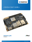
1
» User Guide «
ULP-COM sA3874i User Guide
Document revision 1.0 Draft 07
www.kontron.com
User’s Guide
» Table of Contents «
1 User Information .................................................................................................... 6
1.1
About This Document .................................................................................................................. 6
1.2
Copyright Notice ........................................................................................................................ 6
1.3
Trademarks ............................................................................................................................... 6
1.4
Quality Standards ....................................................................................................................... 6
1.5
Warranty ................................................................................................................................... 6
1.6
Technical Support ...................................................................................................................... 7
2 Introduction .......................................................................................................... 8
2.1
Feature Set Overview .................................................................................................................. 8
2.2
Software Support / Hardware Abstraction ....................................................................................... 9
2.3
Document and Standards References ............................................................................................. 9
2.3.1
External Industry Standard Documents ................................................................................... 9
2.3.2
Kontron Documents ........................................................................................................... 10
2.3.3
Kontron Schematics .......................................................................................................... 10
2.3.4
Texas Instruments Hardware Documents ............................................................................... 10
2.3.5
Texas Instruments Software Documents ................................................................................ 10
2.3.6
Kontron Software BSP ........................................................................................................ 10
3 Specifications ....................................................................................................... 11
2
3.1
Functional Block Diagram .......................................................................................................... 11
3.2
ULP-COM sA3874i General Functions ............................................................................................ 12
3.2.1
ULP-COM sA3874i Feature Set ............................................................................................. 12
3.2.2
Form Factor ..................................................................................................................... 13
3.2.3
CPU ................................................................................................................................ 13
3.2.4
Module Memory ................................................................................................................ 13
3.2.5
On-board Storage .............................................................................................................. 13
3.2.6
Clocks ............................................................................................................................. 13
3.2.7
LVDS Serialized LCD Display Interface ................................................................................... 14
3.2.8
Parallel LCD Display Interface.............................................................................................. 17
3.2.9
Carrier Based 24 bit Color Depth LVDS .................................................................................. 20
3.2.10
High-Definition-Multimedia-Interface (HDMI) Interface ............................................................ 23
www.kontron.com
User’s Guide
3.2.11
Parallel Camera Interface ................................................................................................... 24
3.2.12
USB Interfaces ................................................................................................................. 26
3.2.13
PCIe Interface .................................................................................................................. 29
3.2.14
SATA Interface ................................................................................................................. 30
3.2.15
Gigabit Ethernet Controller (GbE) Interface ........................................................................... 31
3.2.16
SDIO Interface ................................................................................................................. 34
3.2.17
SDMMC Interface for Carrier eMMC ........................................................................................ 35
3.2.18
SPI Interfaces .................................................................................................................. 36
3.2.19
I2S Interfaces .................................................................................................................. 37
3.2.20
SPDIF Interface ................................................................................................................ 38
3.2.21
Asynchronous Serial Ports .................................................................................................. 38
3.2.22
CAN Interface ................................................................................................................... 40
3.2.23
I2C Interface ................................................................................................................... 41
3.3
ULP-COM sA3874i Debug ........................................................................................................... 43
3.3.1
Serial Port for Linux Debug ................................................................................................. 43
3.3.2
AM3874 CPU JTAG ............................................................................................................. 43
3.4
Mechanical Specifications .......................................................................................................... 44
3.4.1
Module Dimensions ........................................................................................................... 44
3.4.2
Height on Top .................................................................................................................. 44
3.4.3
Height on Bottom ............................................................................................................. 44
3.4.4
Layout Diagrams ............................................................................................................... 44
3.4.5
Module Assembly Hardware ................................................................................................. 46
3.4.6
Module Cooling Solution Attachment .................................................................................... 46
3.5
Electrical Specification .............................................................................................................. 47
3.5.1
Supply Voltage ................................................................................................................. 47
3.5.2
RTC/Backup Voltage .......................................................................................................... 47
3.5.3
No Separate Standby Voltage .............................................................................................. 47
3.5.4
Module I/O Voltage ........................................................................................................... 47
3.5.5
Power Consumption ........................................................................................................... 48
3.6
Environmental Specification ....................................................................................................... 49
3.6.1
Operating Temperature ...................................................................................................... 49
3.6.2
Humidity ......................................................................................................................... 49
3.6.3
RoHS Compliance .............................................................................................................. 49
4 Connectors ........................................................................................................... 50
4.1
3
ULP-COM sA3874i Edge Connector Pin Mapping ............................................................................. 50
www.kontron.com
User’s Guide
4.2
JTAG ...................................................................................................................................... 64
4.2.1
Connector J2 CPU JTAG ...................................................................................................... 64
4.2.2
Connector J1 – CPLD JTAG .................................................................................................. 65
5 ULP-COM sA3874i Special Features ........................................................................... 67
5.1
Watchdog Timer ....................................................................................................................... 67
5.2
PMU GPIO ............................................................................................................................... 67
5.3
ULP-COM sA3874i I/O ............................................................................................................... 68
5.4
Temperature Sensor .................................................................................................................. 71
5.5
ULP-COM sA3874i Power Management .......................................................................................... 71
5.6
Board ID EEPROM ..................................................................................................................... 71
6 Thermal Design Considerations ................................................................................ 72
6.1
Thermal Management ................................................................................................................ 72
6.2
Heat Spreader Dimensions ......................................................................................................... 72
6.3
Thermal Parameters .................................................................................................................. 73
6.4
Operation without a Heat Spreader / Heat Sink ............................................................................. 73
7 ULP-COM sA3874i Software ..................................................................................... 74
7.1
Introduction ........................................................................................................................... 74
7.2
Linux EZ Software Development Kit ............................................................................................. 74
7.3
ULP-COM sA3874i Linux Modifications ......................................................................................... 74
7.4
Kontron BSP (Board Support Package) ......................................................................................... 74
8 ULP-COM sA3874i Boot Brief ................................................................................... 75
8.1
ULP-COM sA3874i Boot Up Sequence ........................................................................................... 75
8.2
BOOT Selection ........................................................................................................................ 76
9 ULP-COM sA3874i Programming Methods ................................................................... 77
9.1
External SD Card Programming .................................................................................................... 77
9.2
SPI Programming ..................................................................................................................... 77
9.3
eMMC Programming .................................................................................................................. 77
10 Appendix A: Major Components BOM ......................................................................... 78
11 Appendix B: Document Revision History .................................................................... 81
4
www.kontron.com
User’s Guide
» Table of Figures «
Figure 1: ULP-COM sA3874i Block Diagram ............................................................................................... 11
Figure 2: Sitara Module LVDS LCD Implementation .................................................................................... 14
Figure 3: Sitara Module Parallel LCD Implementation ................................................................................. 17
Figure 4: External USB Port Power Distribution Logic Implementation .......................................................... 27
Figure 5: USB Power Distribution Implementation on Carrier....................................................................... 28
Figure 6: GbE Controller Implementation ................................................................................................. 31
Figure 7: ULP-COM sSA3874I Top Side Components ................................................................................... 44
Figure 8: ULP-COM sA3874i Top Side Components (Labeled) ....................................................................... 45
Figure 9: ULP-COM sA3874i Bottom Side Components ................................................................................ 45
Figure 10: ULP-COM sA3874i Edge View ................................................................................................... 46
Figure 11: ULP-COM sA3874i edge finger primary pins ............................................................................... 50
Figure 12: ULP-COM sA3874i edge finger secondary pins ............................................................................ 50
Figure 13: ULP-COM sA3874i JTAG Connectors .......................................................................................... 64
Figure 14: TI Cortex A8 CPU JTAG........................................................................................................... 64
Figure 15: CPLD JTAG ........................................................................................................................... 65
Figure 16: Heat Spreader ...................................................................................................................... 72
Figure 17: Boot Selection Strap Implementation ....................................................................................... 76
5
www.kontron.com
User’s Guide
1
User Information
1.1
About This Document
This document provides information about products from Kontron and/or its subsidiaries. No warranty of
suitability, purpose, or fitness is implied. While every attempt has been made to ensure that the information in
this document is accurate, the information contained within is supplied “as-is” and it is subject to change
without notice.
For the circuits, descriptions and tables indicated, Kontron assumes no responsibility as far as patents or other
rights of third parties are concerned.
1.2
Copyright Notice
Copyright © 2012 Kontron America Inc.
All rights reserved. No part of this document may be reproduced, transmitted, transcribed, stored in a retrieval
system, or translated into any language or computer language, in any form or by any means (electronic,
mechanical, photocopying, recording, or otherwise), without the express written permission from Kontron.
1.3
Trademarks
Sitara, ARM and all other products and trademarks mentioned in this manual are trademarks of their respective
owners.
1.4
Quality Standards
Kontron is certified to ISO 9000 Quality Standards.
1.5
Warranty
This Kontron product is warranted against defects in material and workmanship for the warranty period from the
date of shipment. During the warranty period, Kontron will at its discretion decide to repair or replace defective
products.
Within the warranty period, the repair of products is free of charge as long as warranty conditions are observed.
The warranty does not apply to defects resulting from improper or inadequate maintenance or handling by the
buyer, unauthorized modification or misuse, operation outside of the product’s environmental specifications or
improper installation or maintenance.
Kontron will not be responsible for any defects or damages to other products not supplied by Kontron that are
caused by a faulty Kontron product.
6
www.kontron.com
User’s Guide
1.6
Technical Support
Technicians and engineers from Kontron and/or its subsidiaries are available for technical support. We are
committed to making our product easy to use and will help you use our products in your systems.
Please consult our website at http://www.kontron.com/support for the latest product documentation, utilities,
drivers and support contacts. Consult our customer section http://emdcustomersection.kontron.com/ for the
latest software downloads, Product Change Notifications and additional tools and software. In any case you can
always contact your board supplier for technical support.
7
www.kontron.com
User’s Guide
2
Introduction
The ULP-COM® (Ultra Low Power – Computer on Module) sA3874i is a versatile small form factor Computer-OnModule that requires low power and provides high performance at low cost. The module connector has 314 edge
fingers that mate with a low profile 314 pin 0.5mm pitch right angle connector (this connector is sometimes
identified as an 321 pin connector, but 7 pins are lost to the key).
Featuring Texas Instruments ARM Cortex A8 microprocessor, Kontron’s ULP-COM sA3874i offers LVDS, Parallel LCD,
HDMI Display, Gigabit Ethernet, PCIe, SATA, USB, USB OTG, Camera support and graphics functions in a cost
effective, low power, miniature package. Kontron’s ULP-COM sA3874i thin and robust design makes it an ideal
building block for reliable system design.
Caution! The ULP-COM sA3874i module is ESD sensitive equipment. Users must observe precautions for handling
electrostatic discharge sensitive devices.
2.1
Feature Set Overview
» ULP-COM compliant in an 82mm x 50mm form factor.
» Texas Instrument single-core 1.0 GHz ARM Cortex A8 SoC.
» Up to 2GB of DDR3 SDRAM support.
» On-board NAND flash eMMC support up to 32GB.
» On-board Atheros (AR8031) GbE PHY.
» Single channel 18bit, 24bit (18 bit compatible) LVDS display panel support.
» HDMI output.
» GPIO support.
» SDIO support.
» I2S support.
» I2C support.
» One Parallel Camera interface.
» One PCIe port.
» USB Host and Client Support.
» Watch Dog Timer (WDT) support.
» UART support.
» CAN support.
» SATA support.
8
www.kontron.com
User’s Guide
2.2
Software Support / Hardware Abstraction
The Kontron sA3874i Module is supported by Kontron BSPs (Board Support Package). The first sA3874i BSP targets
Linux support and is available under Kontron part number xxx-xxx-00. BSPs for other operating systems are
planned. Check with your Kontron contact for the latest BSPs.
This manual goes into a lot of detail on I/O particulars – information is provided on exactly how the various ULPCOM edge fingers tie into the Texas Instruments ARM SoC and to other Module hardware. This is provided for
reference and context. Most of the I/O particulars are covered and abstracted in the BSP and it should generally
not be necessary for sA3874i users to deal with I/O at the register level.
2.3
Document and Standards References
2.3.1 External Industry Standard Documents
» eMMC (Embedded Multi-Media Card) the eMMC electrical standard is defined by JEDEC JESD84-B45 and the
mechanical standard by JESD84-C44 (www.jedec.org).
» GbE MDI (Gigabit Ethernet Medium Dependent Interface) defined by IEEE 802.3. The 1000Base-T
operation over copper twisted pair cabling is defined by IEEE 802.3ab (www.ieee.org).
» HDMI Specification, Version 1.3a, November 10, 2006 © 2006 Hitachi and other companies
(www.hdmi.org).
» The I2C Specification, Version 2.1, January 2000, Philips Semiconductor (now NXP) (www.nxp.com).
» I2S Bus Specification, Feb. 1986 and Revised June 5, 1996, Philips Semiconductor (now NXP)
(www.nxp.com).
» JTAG (Joint Test Action Group) defined by IEEE 1149.1-2001 - IEEE Standard Test Access Port and
Boundary Scan Architecture (www.ieee.org).
» MXM3 Graphics Module Mobile PCI Express Module Electromechanical Specification, Version 3.0, Revision
1.1, © 2009 NVIDIA Corporation (www.mxm-sig.org).
» PICMG® EEEP Embedded EEPROM Specification, Rev. 1.0, August 2010 (www.picmg.org).
» PCI Express Specifications (www.pci-sig.org).
» Serial ATA Revision 3.1, July 18, 2011, Gold Revision, © Serial ATA International Organization (www.sataio.org).
» SD Specifications Part 1 Physical Layer Simplified Specification, Version 3.01, May 18, 2010, © 2010 SD
Group and SD Card Association (Secure Digital) (www.sdcard.org).
» SPDIF (aka S/PDIF) (Sony Philips Digital Interface) - IEC 60958-3.
» SPI Bus – “Serial Peripheral Interface” – de-facto serial interface standard defined by Motorola. A good
description may be found on Wikipedia (http://en.wikipedia.org/wiki/Serial_Peripheral_Interface_Bus).
» USB Specifications (www.usb.org).
9
www.kontron.com
User’s Guide
2.3.2 Kontron Documents
» Ultra Low Power – Computer On Module Hardware Specification, version 1.2, September 19, 2012. ©
Kontron 2012.
» Ultra Low Power – Computer On Module “Evaluation Carrier” User Manual , Version 1.0, September 10,
2012. © Kontron 2012.
» Ultra Low Power – Computer On Module “Evaluation Carrier” Quick Start Manual, Version 1.0, September
10, 2012. © Kontron 2012.
2.3.3 Kontron Schematics
The following schematic numbers are listed for reference. The Module schematic is not usually available outside of
Kontron, without special permission. The other schematics may be available, under NDA or otherwise. Contact
your Kontron representative for more information. The ULP-COM Evaluation Carrier schematic is particularly useful
as an example of the implementation of various interfaces on a Carrier board.
» sA3874i Module, KAI 501-149, latest revision.
» ULP-COM Evaluation Carrier (KARMA Eval Carrier) Board Schematic, KAI 501-146, latest revision.
» eMMC Mezzanine Schematic, KAI 501-151, latest revision.
» KLAS Schematic, Hyundai 1366 x 768 Single Ch. LVDS, KAI 501-162, latest revision.
» KLAS Schematic, NEC 1280 x 768 Single Ch. LVDS, KAI 501-163, latest revision.
2.3.4 Texas Instruments Hardware Documents
» AM387x Sitara ARM Processors Datasheet SPRS695B, Rev B, Sept. 14, 2012.
» AM387x Sitara Technical Reference Manual S PRUGZ7B, Rev B, July 24, 2012.
2.3.5 Texas Instruments Software Documents
» Linux EZ Software Development Kit for Sitara ARM Microprocessors LINUXEZSDK-Sitara, July 27, 2012
2.3.6 Kontron Software BSP
» Kontron BSP for ULP-COM sA3874i Module - Kontron part number xxx-xxx-00.
10
www.kontron.com
User’s Guide
3
Specifications
3.1
Functional Block Diagram
JTAG
Conn
JTAG
Conn
314 Pin 0.5mm pitch
edge finger pattern for
use with MXM3 style
carrier board connector
(aka the “ULP-COM
Carrier Connector”)
Power In (3.0V to 5.25V DC)
Various
Module
Supplies
Power
Supplies
I2C_PM
CPLD_JTAG
JTAG
Boot Straps
1 GB DDR3-800
Memory
DDR3
256M x 8
DDR3
256M x 8
Boot Device Select
Misc
Logic
Misc Ctrl Out
Misc Ctrl In
DDR A
DQ31-DQ24
Misc Ctrl Out (Reset etc)
Misc Ctrl In (Pwr Btn etc)
Actual pin order on the
connector will differ
from what is implied
here.
RGB LCD Data and Control
DDR A
DQ23-DQ16
LVDS
Xmiter
18 / 24 Bit
LVDS
PXL Clock
Divider
Dual Pixel CK
24 bit LVDS requires
display to be
“18 bit compatible”
HDMI
DDR3
256M x 8
DDR3
256M x 8
DDR A
DQ15-DQ8
No CSI Functions
on this Module
Parallel Camera Interface – up to 16 bit
DDR A
DQ7-DQ0
WDTO
GPIO (12 Bit) / PWM / Tach
TI AM3874
2nd GB DDR3 Memory
(Build option)
DDR3
256M x 8
DDR3
256M x 8
DDR3
256M x 8
DDR B
DQ31-DQ24
DDR B
DQ23-DQ16
DDR B
DQ15-DQ8
“Sitara”
ARM Cortex A8
UARTs (2x 2 Wire and 2x 4 Wire)
SDIO (4 Bit)
SDIO / eMMC (8 Bit)
CAN (2 instances)
Single Core
800MHz / 1 GHz
Industrial
Temp
Interfaces shown in gray
and with N/C designation
are not used on this
module but may be used
on other modules
Serial
EEPROM
S/N etc
SPI Flash
8MB
I2C_PM
SPI (2x)
I2C (4x)
I2S / DAP (4 instances)
DDR3
256M x 8
DDR B
DQ7-DQ0
SPDIF Out
SPDIF In
Micron
Industrial
eMMC
Flash Memory
SDDIF
Receiver
DIR9001
SPDIF In
SATA
N/C
8 bit
USB Host
Build options
4GB up to
32GB
USB1
USB0
USB OTG / Client
N/C
N/C
PCIe x1 Gen 2 Root or End Point
N/C
82mm x 50mm Form Factor
PCIe_C
PCIe_B
PCIe_A
RGMII
GBE XCVR
Atheros
AR8031
USB2
Options shown in this
diagram are in the design,
but may not be available
in the standard product
offerings
AFB
MDI - 4 pairs for GBE
(plus support signals – LEDs, etc)
Figure 1: ULP-COM sA3874i Block Diagram
11
www.kontron.com
User’s Guide
3.2
ULP-COM sA3874i General Functions
This section lists the feature set supported by the ULP-COM sA3874i module.
3.2.1 ULP-COM sA3874i Feature Set
The following table summarizes the ULP-COM features implemented on the sA3874i, vs. the maximum possible
allowed in the ULP-COM specification. All mandatory features required by the ULP-COM specification are
implemented in the sA3874i Module.
12
ULP-COM Feature specification
ULP-COM Specification
Maximum Number
Possible
ULP-COM sA3874i
Feature support
ULP-COM sA3874i
Feature support
instances
LVDS Display support
1
Yes
1
Parallel LCD support
1
Yes
1
HDMI Display support
1
Yes
1
CSI Camera support
2
No
0
Parallel Camera support
2
Yes
1
USB Interface
3
Yes
2
PCIe Interface
3
Yes
1
SATA Interface
1
Yes
1
GbE Interface
1
Yes
1
SDIO Interface
1
Yes
1
SDMMC Interface
1
Yes
1
SPI Interface
2
Yes
2
I2S Interface
3
Yes
3
I2C Interface
5
Yes
5
CAN
2
Yes
2
AFB
1
No
0
I/O Voltage (1.8V) level
Yes
I/O Voltage (3.3V) level
No
www.kontron.com
User’s Guide
3.2.2 Form Factor
The ULP-COM sA3874i module complies with the ULP-COM General Specification module size requirements in an
82mm x 50mm form factor.
3.2.3 CPU
The ULP-COM sA3874i module implements Texas Instruments Sitara ARM Cortex A8 microprocessor.
» 45nm AM3874 Cortex A8 1.0 GHz Single core.
» 32 KB Instruction cache and 32 KB Data cache
» 512 KB L2 cache
» 128 KB on-chip memory controller
» 23.0 x 23.0 mm 684-pin FCBGA package.
» Allowable CPU junction temperature range: -40 0C to 90 0C
3.2.4 Module Memory
The ULP-COM sA3874i module supports 1GB and 2GB total DDR3L memory, through two separate orderable SKU’s:
» 51002-1000-08-1
ULP-COM-sA3874i 800 MHz, 1GB memory
» 51002-2000-08-1
ULP-COM-sA3874i 800 MHz, 2GB memory
Additional SKUs may become available. SKU variations would include alternative eMMC options, including possibly
no on-Module eMMC. Check with your Kontron contact or on the Kontron web site for updated information.
3.2.5 On-board Storage
The ULP-COM sA3874i module supports SPI flash memory devices with build options from 4 GB up to 32 GB. The
standard SKUs support 4 GB eMMC flash.
3.2.6 Clocks
A 32.768 KHz clock is required for the Sitara ARM Cortex CPU RTC (Real Time Clock) and PMC (Power Management
Controller). This clock is provided by Power Management Unit (PMU).
13
www.kontron.com
User’s Guide
3.2.7 LVDS Serialized LCD Display Interface
The LVDS color packing used on the Module is in the “18 bit color compatible mode” (more details on this can be
found later in this section and in the Ultra Low Power – Computer On Module Hardware Specification ). The display
connection may be 18 bit or 24 bit, but if a 24 bit connection is used, then the display must be capable of
accepting an “18 bit color packing”. This is sometimes alternatively referred to as “6 bit pack” (it’s 6 bits per
color, or 18 bits total …). For single channel LVDS, a display resolution up to approximately 1280 x 1024 may be
supported (approximate” because factors such as Carrier Board trace lengths, routing quality, cable length and
quality, Carrier EMI and ESD suppression device selections and display timing particulars can affect the maximum
resolution achieved). For high resolution displays (1280 x 1024 and higher), a Carrier Board based dual channel
LVDS transmitter operating from the Module parallel data path should be used instead.
For flat panel use, parallel LCD data and control information (Red, Green and Blue color data, Display Enable,
Vertical Synch and Horizontal Synch) are serialized onto a set of LVDS differential pairs. The information is packed
into frames that are 7 bits long. For 18 bit color depths, the data and control information utilize three LVDS
channels (18 data bits + 3 control bits = 21 bits; hence 3 channels with 7 bit frames) plus a clock pair. For 24 bit
color depths, four LVDS channels are used (24 data bits + 3 control bits + 1 unused bit = 28 bits, or 4 x 7) plus a
clock pair. The LVDS clock is transmitted on a separate LVDS pair. The LVDS clock period is 7 times longer than the
pixel clock period. The LVDS clock edges are off from the 7 bit frame boundaries by 2 pixel periods. Unfortunately,
there are two different 24 bit color mappings in use. The more common one, sometimes referred to as “24 bit
standard color mapping” is not compatible with 18 bit panels, as it places the most significant RGB color data on
the 4th LVDS data pair – the pair that is not used on 18 bit panels. There is a less common “24 bit / 18 bit
compatible” mapping that puts the least significant color bits of the 24 bit set onto the 4 th LVDS pair and allows
24 bit color depths.
VOUT0_B[0:7]
H2
H1
LVDS0+
LVDS0-
S125
S126
VOUT0_G[0:7]
G2
VOUT0_R[0:7]
AC11
AB13
AD12
VOUT0_AVID
VOUT0_HSYNC
VOUT0_VSYNC
VOUT0_CLK
LVDS
XMITTER
E2
(U19)
TI
A3
E1
SN65LVDS93AZ
A4
B4
C2
C1
A2
D2
D1
LVDS2+
LVDS2-
LVDS3+
LVDS3-
LVDS_CK+
LVDS_CK-
S128
S129
S131
S132
EDGE FINGER
(J3)
SITARA CPU
(U7)
AA10
G1
LVDS1+
LVDS1-
S137
S138
S134
S135
Figure 2: Sitara Module LVDS LCD Implementation
14
www.kontron.com
User’s Guide
The following table details exactly how the Sitara ARM CPU parallel LCD pins are mapped to the on-Module Texas
Instruments SN65LVDS93AZ LVDS transmitter. For 18 bit displays, LVDS channels 0, 1 and 2 are used. For 24 bit
displays (that accept 18 bit color packing), channels 0, 1, 2 and 3 are used.
15
18 Bit
standard
Color
mapping
24 Bit/18
bit
compatible
Color
mapping
Pin #
Pin Name
Pin #
Pin Name
AB8
VOUT[0]_G_Y_YC[4]
K5
D7
VOUT0_G[2]
1
G0
G2
AC13
VOUT[0]_R_CR[9]
J4
D6
VOUT0_R[7]
2
R5
R7
AE8
VOUT[0]_R_CR[8]
K3
D4
VOUT0_R[6]
3
R4
R6
AF12
VOUT[0]_R_CR[7]
J3
D3
VOUT0_R[5]
4
R3
R5
AF6
VOUT[0]_R_CR[6]
K2
D2
VOUT0_R[4]
5
R2
R4
AF8
VOUT[0]_R_CR[5]
K1
D1
VOUT0_R[3]
6
R1
R3
AA9
VOUT[0]_R_CR[4]
J2
D0
VOUT0_R[2]
7
R0
R2
AD15
VOUT[0]_B_CB_C[5]
D5
D18
VOUT0_B[3]
1
B1
B3
AD11
VOUT[0]_B_CB_C[4]
E5
D15
VOUT0_B[2]
2
B0
B2
AF14
VOUT[0]_G_Y_YC[9]
F6
D14
VOUT0_G[7]
3
G5
G7
AE14
VOUT[0]_G_Y_YC[8]
G6
D13
VOUT0_G[6]
4
G4
G6
AD14
VOUT[0]_G_Y_YC[7]
G5
D12
VOUT0_G[5]
5
G3
G5
AA8
VOUT[0]_G_Y_YC[6]
J6
D9
VOUT0_G[4]
6
G2
G4
AB12
VOUT[0]_G_Y_YC[5]
K6
D8
VOUT0_G[3]
7
G1
G3
AA10
VOUT[0]_AVID/VOUT
[0]_FLD
A3
D26
VOUT0_AVID
1
DE
DE
AB13
VOUT[0]_VSYNC
B4
D25
VOUT0_VSYNC
2
VS
VS
AC11
VOUT[0]_HSYNC
A4
D24
VOUT0_HSYNC
3
HS
HS
AG15
VOUT[0]_B_CB_C[9]
A6
D22
VOUT0_B[7]
4
B5
B7
AF15
VOUT[0]_B_CB_C[8]
B5
D21
VOUT0_B[6]
5
B4
B6
AB10
VOUT[0]_B_CB_C[7]
B6
D20
VOUT0_B[5]
6
B3
B5
Net names
0
1
2
Transmit Bit
Order
LVDS Transmitter
(TI
SN65LVDS93AZ)
LVDS Channel
Sitara ARM Cortex CPU
www.kontron.com
User’s Guide
16
7
B2
B4
Not Used
1
Not Used
Not Used
D17
VOUT0_B[1]
2
Not Used
B1
E6
D16
VOUT0_B[0]
3
Not Used
B0
VOUT[0]_G_Y_YC[3]
H6
D11
VOUT0_G[1]
4
Not Used
G1
AH7
VOUT[0]_G_Y_YC[2]
H4
D10
VOUT0_G[0]
5
Not Used
G0
AB9
VOUT[0]_R_CR[3]
K4
D5
VOUT0_R[1]
6
Not Used
R1
AD9
VOUT[0]_R_CR[2]
J1
D27
VOUT0_R[0]
7
Not Used
R0
AD12
VOUT[0]_CLK
A2
CLKIN
VOUT0_CLK
Sitara ARM Cortex CPU
Net names
AC10
VOUT[0]_B_CB_C[6]
C6
D19
VOUT0_B[4]
Not
Used
Not Used
A5
D23
AE15
VOUT[0]_B_CB_C[3]
D6
AG7
VOUT[0]_B_CB_C[2]
AH15
3
Transmit Bit
Order
24 Bit/18
bit
compatible
Color
mapping
LVDS Channel
18 Bit
standard
Color
mapping
LVDS Transmitter
(TI
SN65LVDS93AZ)
www.kontron.com
User’s Guide
3.2.8 Parallel LCD Display Interface
The Sitara ARM CPU parallel 24 bit LCD interface is brought to the Module edge connector. The interface runs at
the 1.8V Module I/O voltage. This voltage swing may be used directly with 1.8V capable Carrier Board LVDS
transmitters, such as the TI SN75LVDS83B. The 1.8V signaling may not be suitable for direct connection to a
parallel flat panel. Generally speaking, only small panels, with screen diagonals of 5” or less, are available with a
1.8V interface. Larger parallel LCD panels are likely to use 3.3V signaling and a set of voltage translators / buffers
would be needed on the Carrier.
RED
VOUT0_R[0:7]
GREEN
VOUT0_G[0:7]
BLUE
VOUT0_B[0:7]
AC11
AB13
AD12
VOUT0_HSYNC
VOUT0_VSYNC
VOUT0_CLK
B11
K9
C10
CPLD
(U20)
A10
S122
S121
S123
LCD_DE
LCD_DUAL_PCK
EDGE FINGER
(J3)
SITARA CPU
(U7)
S120
S142
B10
Figure 3: Sitara Module Parallel LCD Implementation
The mapping of the Sitara CPU parallel LCD balls to the ULP-COM edge connector is shown in the table below. For
24 bit implementations, all bits are used. For 18 bit implementations, in ULP-COM, the least significant bits (Red
D17:16, Green D9:8, Blue D1:0) are dropped.
17
www.kontron.com
User’s Guide
18
24 bit
Color
map
Sitara TI ARM Cortex CPU
ULP-COM sA3874i Edge
finger
Pin #
Pin Name
Pin #
Pin Name
AC13
VOUT[0]_R_CR[9]
S118
LCD_D23
VOUT0_R[7]
R7
AE8
VOUT[0]_R_CR[8]
S117
LCD_D22
VOUT0_R[6]
R6
AF12
VOUT[0]_R_CR[7]
S116
LCD_D21
VOUT0_R[5]
R5
AF6
VOUT[0]_R_CR[6]
S115
LCD_D20
VOUT0_R[4]
R4
AF8
VOUT[0]_R_CR[5]
S114
LCD_D19
VOUT0_R[3]
AA9
VOUT[0]_R_CR[4]
S113
LCD_D18
VOUT0_R[2]
R2
AB9
VOUT[0]_R_CR[3]
S112
LCD_D17
VOUT0_R[1]
R1
AD9
VOUT[0]_R_CR[2]
S111
LCD_D16
VOUT0_R[0]
R0
AF14
VOUT[0]_G_Y_YC[9]
S109
LCD_D15
VOUT0_G[7]
G7
AE14
VOUT[0]_G_Y_YC[8]
S108
LCD_D14
VOUT0_G[6]
G6
AD14
VOUT[0]_G_Y_YC[7]
S107
LCD_D13
VOUT0_G[5]
G5
AA8
VOUT[0]_G_Y_YC[6]
S106
LCD_D12
VOUT0_G[4]
G4
AB12
VOUT[0]_G_Y_YC[5]
S105
LCD_D11
VOUT0_G[3]
AB8
VOUT[0]_G_Y_YC[4]
S104
LCD_D10
VOUT0_G[2]
G2
AH15
VOUT[0]_G_Y_YC[3]
S103
LCD_D9
VOUT0_G[1]
G1
AH7
VOUT[0]_G_Y_YC[2]
S102
LCD_D8
VOUT0_G[0]
G0
AG15
VOUT[0]_B_CB_C[9]
S100
LCD_D7
VOUT0_B[7]
B7
AF15
VOUT[0]_B_CB_C[8]
S99
LCD_D6
VOUT0_B[6]
B6
AB10
VOUT[0]_B_CB_C[7]
S98
LCD_D5
VOUT0_B[5]
B5
AC10
VOUT[0]_B_CB_C[6]
S97
LCD_D4
VOUT0_B[4]
B4
AD15
VOUT[0]_B_CB_C[5]
S96
LCD_D3
VOUT0_B[3]
AD11
VOUT[0]_B_CB_C[4]
S95
LCD_D2
VOUT0_B[2]
B2
AE15
VOUT[0]_B_CB_C[3]
S94
LCD_D1
VOUT0_B[1]
B1
AG7
VOUT[0]_B_CB_C[2]
S93
LCD_D0
VOUT0_B[0]
B0
GREEN
RED
Color
BLUE
Net Name
R3
G3
B3
www.kontron.com
User’s Guide
19
Sitara TI ARM Cortex CPU
ULP-COM sA3874i Edge
finger
Net Name
AD12
VOUT[0]_CLK
S123
LCD_PCK
VOUT0_CLK
AA10
VOUT[0]_AVID/VOUT[0]_FLD
S120
LCD_DE
VOUT0_AVID/LCD_DE
AC11
VOUT[0]_HSYNC
S122
LCD_HS
VOUT0_HSYNC
AB13
VOUT[0]_VSYNC
S121
LCD_VS
VOUT0_VSYNC
Color
24 bit
Color
map
www.kontron.com
User’s Guide
3.2.9 Carrier Based 24 bit Color Depth LVDS
The Module parallel LCD path may be used to implement single or dual channel Carrier Board LVDS transmitter(s).
The color packing may be 24 bit or 18 bit. Since 18 bit single channel color packing is already available from the
Module LVDS, only 24 bit color packing is described in this section.
A single channel implementation uses one SN75LVDS83B (or equivalent) LVDS transmitter and a dual channel
implementation uses one Thine THC63LVD827 (or equivalent) LVDS transmitter. The same dual channel LVDS
transmitter can be used for single channel LVDS implementation, if the feature is available on the transmitter.
The following table shows how the sA3874i LCD pins should be mapped to TI SN75LVDS83B, for standard single
channel LVDS 24 bit color packing. The chart shows pin numbers for the BGA version of the part. The TSSOP
version can be used as well, although the pin numbering is different. The pin names remain the same.
Transmitters from other vendors may be used as well.
ULP-COM sA3874i Edge finger
LVDS Transmitter
(TI SN75LVDS83B)
Pin #
Pin Name
Pin #
Pin Name
S102
LCD_D8
K5
S116
LCD_D21
S115
LVDS
Channel
Transmit
bit Order
24 bit standard color
mapping
D7
1
G0
J4
D6
2
R5
LCD_D20
K3
D4
3
R4
S114
LCD_D19
J3
D3
4
R3
S113
LCD_D18
K2
D2
5
R2
S112
LCD_D17
K1
D1
6
R1
S111
LCD_D16
J2
D0
7
R0
S94
LCD_D1
D5
D18
1
B1
S93
LCD_D0
E5
D15
2
B0
S107
LCD_D13
F6
D14
3
G5
S106
LCD_D12
G6
D13
4
G4
S105
LCD_D11
G5
D12
5
G3
S104
LCD_D10
J6
D9
6
G2
S103
LCD_D9
K6
D8
7
G1
S120
LCD_DE
A3
D26
1
DE
2
VS
0
1
2
S121
20
LCD_VS
B4
D25
www.kontron.com
User’s Guide
ULP-COM sA3874i Edge finger
LVDS Transmitter
(TI SN75LVDS83B)
S122
LCD_HS
A4
S98
LCD_D5
S97
LVDS
Channel
Transmit
bit Order
24 bit standard color
mapping
D24
3
HS
A6
D22
4
B5
LCD_D4
B5
D21
5
B4
S96
LCD_D3
B6
D20
6
B3
S95
LCD_D2
C6
D19
7
B2
N/C
N/C
A5
D23
1
Not Used
S100
LCD_D7
D6
D17
2
B7
S99
LCD_D6
E6
D16
3
B6
S109
LCD_D15
H6
D11
4
G7
S108
LCD_D14
H4
D10
5
G6
S118
LCD_D23
K4
D5
6
R7
S117
LCD_D22
J1
D27
7
R6
S123
LCD_PCK
A2
CLKIN
3
Pixel clock
The following table shows how the sA3874i LCD pins should be mapped to Thine THC63LVD82, for standard dual
channel LVDS 24 bit color packing. Other LVDS 24 bit mapping can be used with this transmitter. Transmitters
from other vendors may be used as well.
21
ULP-COM sA3874i Edge finger
LVDS Transmitter
(Thine THC63LVD82)
Pin #
Pin Name
Pin #
Pin Name
S102
LCD_D8
H1
S116
LCD_D21
S115
LVDS
Channel
Transmit
bit Order
24 bit standard color
mapping
G10
1
G0
F1
R15
2
R5
LCD_D20
F2
R14
3
R4
S114
LCD_D19
E1
R13
4
R3
S113
LCD_D18
E2
R12
5
R2
S112
LCD_D17
D1
R11
6
R1
S111
LCD_D16
D2
R10
7
R0
0
www.kontron.com
User’s Guide
ULP-COM sA3874i Edge finger
LVDS Transmitter
(Thine THC63LVD82)
S94
LCD_D1
J5
S93
LCD_D0
S107
LVDS
Channel
Transmit
bit Order
24 bit standard color
mapping
B11
1
B1
H5
B10
2
B0
LCD_D13
J3
G15
3
G5
S106
LCD_D12
H3
G14
4
G4
S105
LCD_D11
J2
G13
5
G3
S104
LCD_D10
H2
G12
6
G2
S103
LCD_D9
J1
G11
7
G1
S120
LCD_DE
G9
DE
1
DE
S121
LCD_VS
H9
VSYNC
2
VS
S122
LCD_HS
J9
HSYNC
3
HS
S98
LCD_D5
J7
B15
4
B5
S97
LCD_D4
H7
B14
5
B4
S96
LCD_D3
J6
B13
6
B3
S95
LCD_D2
H6
B12
7
B2
N/C
N/C
1
Not Used
S100
LCD_D7
J8
B17
2
B7
S99
LCD_D6
H8
B16
3
B6
S109
LCD_D15
J4
G17
4
G7
S108
LCD_D14
H4
G16
5
G6
S118
LCD_D23
G1
R17
6
R7
S117
LCD_D22
G2
R16
7
R6
S123
LCD_PCK
F9
CLKIN
1
2
3
Pixel clock
A very good, lower cost alternative to the Thine THC63LVD82 dual channel LVDS transmitter is the TI DS90C187
dual channel LVDS transmitter. A future version of this manual will replace the Thine references with a TI
DS90C187 reference. The module Design Guide is being written up with the TI DS90C187 as the example.
22
www.kontron.com
User’s Guide
3.2.10 High-Definition-Multimedia-Interface (HDMI) Interface
The ULP-COM sA3874i module supports a single HDMI interface with a resolution up to 1920x1080 pixels.
HDMI signals are exposed on the ULP-COM sA3874i edge connector as shown below:
ULP-COM sA3874i Edge finger
TI Cortex A8 CPU
Pin #
Pin #
Pin Name
Pin Name
Net Name
Notes
HDMI
Differential
Data pair
0 output
HDMI Differential Signals
P98
HDMI_D0_P
AG19
HDMI_DP0
HDMI_D0+
P99
HDMI_D0_N
AH19
HDMI_DN0
HDMI_D0-
P95
HDMI_D1_P
AG20
HDMI_DP1
HDMI_D1+
P96
HDMI_D1_N
AH20
HDMI_DN1
HDMI_D1-
P92
HDMI_D2_P
AG21
HDMI_DP2
HDMI_D2+
P93
HDMI_D2_N
AH21
HDMI_DN2
HDMI_D2-
P101
HDMI_CK_P
AG18
HDMI_CLKP
HDMI_CK+
P102
HDMI_CK_N
AH18
HDMI_CLKN
HDMI_CK-
HDMI
Differential
Data pair 1
output
HDMI
Differential
Data pair 2
output
HDMI
Differential
clock output
HDMI Support signals
P104
HDMI_HPD
AA26
HDMI_HPDET
HDMI_HPD
HDMI Hot Plug
Detect input
P105
HDMI_CTRL_CK
AF24
HDMI_SCL
HDMI_DDC_SCL_1V8
HDMI dedicated
I2C Clock
P106
HDMI_CTRL_DAT
AG24
HDMI_CNTL_DAT
HDMI_DDC_SDA_1V8
HDMI dedicated
I2C Data
P107
HDMI_CEC
AB27
HDMI_CEC
HDMI_CEC
Not used
The Carrier board must provide voltage translation for the DDC and HPD signals, as well as ESD protection on all
the HDMI signals. The Carrier board ESD protection is important as HDMI is a hot-pluggable interface. A device
such as the Texas Instruments TPD12S016 is recommended. The Kontron ULP-COM Evaluation Board schematic
(KAI 501-146) is useful as an implementation example.
23
www.kontron.com
User’s Guide
3.2.11 Parallel Camera Interface
The ULP-COM sA3874i module supports one parallel camera interface. The parallel camera interface signals are
exposed on the ULP-COM sA3874i edge connector as shown below:
ULP-COM sA3874I Edge finger
TI Cortex A8 CPU
Pin #
Pin #
Pin Name
Pin Name
Net Name
Notes
Parallel camera input
data
PCAM SIGNALS
24
P3
PCAM_D0/CSI1_CK_P
AF9
VIN[0]A_D[0]
PCAM_D[0]
P4
PCAM_D1/CSI1_CK_N
AB11
VIN[0]A_D[1]
PCAM_D[1]
P7
PCAM_D2/ CSI1_D0_P
AC9
VIN[0]A_D[2]
PCAM_D[2]
P8
PCAM_D3/ CSI1_D0_N
AE12
VIN[0]A_D[3]
PCAM_D[3]
P10
PCAM_D4/CSI1_D1_P
AH8
VIN[0]A_D[4]
PCAM_D[4]
P11
PCAM_D5/CSI1_D1_N
AG16
VIN[0]A_D[5]
PCAM_D[5]
P13
PCAM_D6/CSI1_D2_P
AH16
VIN[0]A_D[6]
PCAM_D[6]
P14
PCAM_D7/CSI1_D2_N
AA11
VIN[0]A_D[7]
PCAM_D[7]
P16
PCAM_D8/CSI1_D3_P
AB15
VIN[0]A_D[8]_BD[
0]
PCAM_D[8]
P17
PCAM_D9/CSI1_D3_N
AG9
VIN[0]A_D[9]_BD[
1]
PCAM_D[9]
S8
PCAM_D10/CSI0_CK_P
AH9
VIN[0]A_D[10]_BD
[2]
PCAM_D[10]
S9
PCAM_D11/CSI0_CK_N
AH17
VIN[0]A_D[11]_BD
[3]
PCAM_D[11]
S11
PCAM_D12/CSI0_D0_P
AG17
VIN[0]A_D[12]_BD
[4]
PCAM_D[12]
S12
PCAM_D13/CSI0_D0_N
AF17
VIN[0]A_D[13]_BD
[5]
PCAM_D[13]
S14
PCAM_D14/CSI0_D1_P
AC12
VIN[0]A_D[14]_BD
[6]
PCAM_D[14]
S15
PCAM_D15/CSI0_D1_N
AC14
VIN[0]A_D[15]_BD
[7]
PCAM_D[15]
www.kontron.com
User’s Guide
ULP-COM sA3874I Edge finger
TI Cortex A8 CPU
Net Name
Notes
S4
PCAM_PXL_CK0
AB20
VIN[0]A_CLK
PCAM_PXL_CK
Parallel camera primary
pixel clock input
P6
PCAM_MCK
AE17
VIN[0]B_CLK
PCAM_MCK
Parallel camera Master
Clock output
S2
PCAM_HSYNC
AC20
VIN[0]A_HSYNC
PCAM_HSYNC
Parallel camera
Horizontal Sync input
S1
PCAM_VSYNC
AD20
VIN[0]A_VSYNC
PCAM_VSYNC
Parallel camera Vertical
Sync input
P5
PCAM_DE
AE21
VIN[0]A_DE
PCAM_DE
Parallel camera Data
Enable input
P115
GPIO7/PCAM_FLD
AA20
VIN[0]A_FLD/VIN[0
]B_VSYNC/UART5_R
XD/I2C[2]_SCL/GP2
[1]
GPIO7/PCAM_FLD
Parallel camera Field
input
AH26
I2C[3]_SCL
I2C_CAM_CK/I2C3
_CK
Parallel camera support
I2C_CAM_DAT/I2C
3_DAT
Parallel camera support
MCA[2]_ACLKX/GP0
[10]
GPIO0/CAM0_PWR
Camera 0 Power Enable,
VIN[0]A_FLD/CAM_
D[5]/GP0[20]
GPIO2/CAM0_RST
PCAM Support signals
S5
S7
P108
P110
25
I2C_CAM_CK
I2C_CAM_DAT
GPIO0 / CAM0_PWR#
GPIO2 / CAM0_RST#
AA24
U6
AC22
I2C[3]_SDA
link - I2C clock
link - I2C data
active low output.
Camera 0 Reset, active
low output
S57
PCAM_ON_CSI0#
GND
Camera type selection
signal
S58
PCAM_ON_CSI1#
GND
Camera type selection
signal
www.kontron.com
User’s Guide
3.2.12 USB Interfaces
The Kontron sA3874i module supports two USB ports (USB 0:1). Per the ULP-COM specification, the Kontron
sA3874i USB0 port is capable of functioning either as a client or host device. The sA3874i module also supports
one additional USB2.0 host port, on ULP-COM USB1. This product does not implement the optional third USB
interface defined in the ULP-COM spec.
USB interface signals are exposed on the ULP-COM sA3874i edge connector as shown below:
ULP-COM sA3874i Edge finger
TI Cortex A8 CPU
Pin #
Pin #
Pin Name
Pin Name
Net Name
Notes
USB0 Port
P60
USB0_P
AG11
USB0_DP
USB0+
P61
USB0_N
AH11
USB0_DM
USB0-
USB0 port data
pair
P63
USB0_VBUS_DET
AG12
USB0_VBUSIN
USB0_VBUS_DET
USB host power
detection, when
this port is used
as a device.
P64
USB0_OTG_ID
AG10
USB0_ID
USB0_OTG_ID
USB OTG ID
input, active
high
USB1 Port
P65
USB1_P
AG13
USB1_DP
USB1+
P66
USB1_N
AH13
USB1_DM
USB1-
USB1 port data
pair
The ULP-COM Hardware specification defines USBx_EN_OC# (where x is 0 and 1 for use with USB0 and USB1) pins
as multifunction pins to use for power enable of USBx ports, as well as for over current indication. The ULP-COM
sA3874i complies with this definition. These nets are provided with pull up resistors on the Module. The Module
CPLD contains the glue logic required for this implementation.
The sA3874i Module USB power-enable and over-current indication logic implementation is shown in the following
block diagram. There are 10K pull-up resistors on the Module on the ULP-COM USBx_EN_OC# lines. The CPLD
outputs driving the USBx_EN_OC# lines are open-drain. The Carrier board USB power switch, if present, is enabled
by virtue of the 10K Module pull-up to 3.3V.
26
www.kontron.com
User’s Guide
EN_USB1_VBUS_1V8
1v8 to 3v3
Translator EN_USB1_VBUS_3V3
SITARA
CPU
(U7)
AE27
AF28
USB0_OC#
USB1_OC#
USB0_OC_3V3#
3v3 to 1v8
Translator
USB1_OC_3V3#
K10
USB0_EN_OC_PU
C1
10K
EN_USB0_VBUS_3V3
B1
CPLD
(U20)
K5
F3
F1
USB0_EN_OC#
P62
USB1_EN_OC_PU
L5
EDGE FINGER
(J3)
L5
EN_USB0_VBUS_1V8
10K
AF11
G1
USB1_EN_OC#
P67
Figure 4: External USB Port Power Distribution Logic Implementation
USB port power enable and over current logic implementation between the TI AM3874CPU and CPLD is shown in
the table below:
TI Cortex A8 CPU
CPLD
Net Name
Notes
Pin #
Pin Name
Pin #
Pin Name
AF11
USB0_DRVVBUS
C1
IO_C1
EN_USB0_VBUS_1V8/
EN_USB0_VBUS_3V3
USB Port0 power enable
L5
USB1_DRVVBUS
B1
IO_B1
EN_USB1_VBUS_1V8/
EN_USB1_VBUS_3V3
USB Port1 power enable
AE27
GMI_AD09
K5
IO_K5
USB0_OC#/
USB0_OC_3V3
USB Port0 over current indication
signal
AF28
GMI_CS1#
L5
IO_L5
USB1_OC#/
USB1_OC_3V3
USB Port1 over current indication
signal
USB port power-enable and over-current logic implementation between the CPLD and ULP-COM sA3874i edge
connector is shown in the table below:
ULP-COM sA3874i
Edge Finger
CPLD
27
Net Name
Notes
Pin #
Pin Name
Pin #
Pin Name
F3
IO_F3
P62
USB0_EN_
OC#
USB0_EN_OC#
USB Port0 power enable/over current
indication signal
G1
IO_G1
P67
USB1_EN_
OC#
USB1_EN_OC#
USB Port1 power enable/over current
indication signal
www.kontron.com
User’s Guide
ULP-COM CARRIER MXM3
CONNECTOR
(J40)
Power distribution for external USB plug-in peripherals (USB memory sticks, cameras, keyboards, mice, etc.) is
typically handled by USB power switches such as the Texas Instruments TPS2052B, Micrel MIC2026-1 or similar
devices on the Carrier board. The Enable pin on the Carrier board USB power switch must be active – high and the
Over-Current pin (OC#) must be open drain, active low (these are commonly available). No pull-up is required on
the USB power switch Enable or OC# line; they are tied together on the Carrier and fed to the Module
USBx_EN_OC# pin. The pull-up is on the Module.
5V
USBx_EN_OC#
Switched
Pwr
Pwr
USBx_VBUS
Enable
TPS2052B
OC#
Figure 5: USB Power Distribution Implementation on Carrier
28
www.kontron.com
User’s Guide
3.2.13 PCIe Interface
The ULP-COM sA3874i module supports one PCIe GEN2 interface. PCIe interface signals are exposed on the ULPCOM sA8374 edge connector as shown below:
29
ULP-COM sA3874i Edge
Finger
IT CORTEX A8 CPU
Net Name
Notes
Pin #
Pin Name
Pin #
Pin Name
P89
PCIE_A_TX_P
AD2
PCIE_TXP0
PCIE_A_TX0+
AD1
PCIE_TXN0
PCIE_A_TX0-
Differential PCIe Link A transmit
data pair 0. Series decoupling
caps are provided in the Module.
P90
PCIE_A_TX_N
P86
PCIE_A_RX_P
AC1
PCIE_RXN0
PCIE_A_RX0+
P87
PCIE_A_RX_N
AC2
PCIE_RXP0
PCIE_A_RX0-
P83
PCIE_A_REFCK_P
PCIE_A_REFCK0+
P84
PCIE_A_REFCK_N
PCIE_A_REFCK0-
P78
PCIE_A_CKREQ#
PCIE_A_CKREQ#
PCIe Port A clock request input
P74
PCIE_A_PRSNT#
PCIE_A_PRSNT#/PC
IE_A_PRSNT_1V8#
PCIe Port A present input
P75
PCIE_A_RST#
PCIE_A_RST#
PCIe Port A reset output, active
low is generated from CPLD
L6
TIM7_IO/GP0[28]
Differential PCIe Link A receive
data pair 0. Series decoupling
caps are not provided in the
Module.
Differential PCIe Link A
reference clock output
www.kontron.com
User’s Guide
3.2.14 SATA Interface
The ULP-COM sA3874i module supports one SATA port. SATA interface signals are exposed on the ULP-COM
sA3874i edge connector as shown below:
30
ULP-COM sSA3874i Edge finger
TI Cortex A8 CPU
Net Name
Notes
Pin #
Pin Name
Pin #
Pin Name
P48
SATA_TX_P
AB2
SATA_TXP0
SATA0_TX+
Differential SATA 0
transmit data Pair.
P49
SATA_TX_N
AB1
SATA_TXN0
SATA0_TX-
Series decoupling
caps are provided
in the Module.
P51
SATA_RX_P
AA1
SATA_RXP0
SATA0_RX+
Differential SATA 0
receive data Pair.
P52
SATA_RX_N
AA2
SATA_RXN0
SATA0_RX-
S54
SATA_ACT#
AE24
VIN[1]A_HSYNC/GP2[28]
SATA_ACT#
Series decoupling
caps are provided
in the Module.
SATA activity
indication
www.kontron.com
User’s Guide
3.2.15 Gigabit Ethernet Controller (GbE) Interface
The ULP-COM sA3874i module supports one GbE interface. This is accomplished by using TI Cortex A8 SoC’s
internal MAC in conjunction with Atheros PHY (AR8031). This is diagrammed below.
G28
G27
F28
H26
J26
H27
L23
L24
J27
H28
P24
RGMII0_TXD[2]
RGMII0_TXD[3]
RGMII0_TXCTL
RGMII0_TXC
RGMII0_RXD[0]
RGMII0_RXD[1]
RGMII0_RXD[2]
RGMII0_RXD[3]
RGMII0_RXCTL
RGMII0_RXC
INT_ETH
MDCLK
MDIO
36
37
38
39
34
35
31
30
28
27
32
33
5
11
12
GBE_MDI0+
GBE_MDI0-
14
GBE_MDI1+
GBE_MDI1-
15
GBE PHY
ATHEROS
AR8031
(U22)
17
18
GBE_MDI2+
GBE_MDI2-
20
21
GBE_MDI3+
GBE_MDI3-
26
24
23
GBE_LINK100#
GBE_LINK1000#
GBE_LINK_ACT#
P30
P29
P27
P26
P24
P23
P20
P19
EDGE FINGER
(J3)
P23
SITARA CPU
R23
(U7)
R25
T23
RGMII0_TXD[0]
RGMII0_TXD[1]
P21
P22
P25
1
48
Figure 6: GbE Controller Implementation
31
www.kontron.com
User’s Guide
The following table details the TI AM3874 to Atheros GBE Phy (AR8031) connection details.
32
TI Cortex A8 CPU
Atheros AR8031
Net Name
Notes
Pin #
Pin Name
Pin #
Pin Name
G28
RGMII0_TXD0
36
TXD0
RGMII0_TXD[0]
GBE controller RGMII transmit
data
G27
RGMII0_TXD1
37
TXD1
RGMII0_TXD[1]
F28
RGMII0_TXD2
38
TXD2
RGMII0_TXD[2]
H26
RGMII0_TXD3
39
TXD3
RGMII0_TXD[3]
J26
RGMII0_TXCTL
34
TXEN
RGMII0_TXCTL
RGMII transmit enable
H27
RGMII0_TXC
35
GTX_CLK
RGMII0_TXC
RGMII transmit clock
P23
RGMII0_RXD0
31
RXD0
RGMII0_RXD[0]
GBE controller RGMII receive data
R23
RGMII0_RXD1
30
RXD1
RGMII0_RXD[1]
R25
RGMIIO_RXD2
28
RXD2
RGMII0_RXD[2]
T23
RGMII0_RXD3
27
RXD3
RGMII0_RXD[3]
L23
RGMII0_RXCTL
32
RX_DV
RGMII0_RXCTL
RGMII receive data valid signal
L24
RGMII0_RXC
33
RX_CLK
RGMII0_RXC
RGMII receive clock output
J27
EMAC_RMREFCLK/TI
M2_IO/GP1[10]
5
INT
INT_ETH
Interrupt signal to system
H28
MDCLK
1
MDC
MDCLK
Management data clock reference
P24
MDIO
48
MDIO
MDIO
Management data
www.kontron.com
User’s Guide
The following table details the Atheros GBE Phy (AR8031) to ULP-COM connections.
33
ULP-COM sA3874i Edge
Finger
Atheros AR8031
Net Name
Notes
Pin #
Pin Name
Pin #
Pin Name
P30
GbE_MDI0_P
11
TRXP0
GBE0_MDI0+
Bi-directional transmit/receive
pair 0 to magnetics
P29
GbE_MDI0_N
12
TRXN0
GBE0_MDI0-
P27
GbE_MDI1_P
14
TRXP1
GbE_MDI1+
P26
GbE_MDI1_N
15
TRXN1
GbE_MDI1-
P24
GbE_MDI2_P
17
TRXP2
GbE_MDI2+
P23
GbE_MDI2_N
18
TRXN2
GbE_MDI2-
P20
GbE_MDI3_P
20
TRXP3
GbE_MDI3+
P19
GbE_MDI3_N
21
TRXN3
GbE_MDI3-
P21
GbE_LINK100#
26
LED_LINK10_100
GBE0_LINK100#
Link speed indication LED for
100Mbps – open drain
P22
GbE_LINK1000#
24
LED_LINK1000
GBE0_LINK1000#
Link speed indication LED for
1000Mbps – open drain
P25
GbE_LINK_ACT#
23
LED_ACT
GBE0_LINK_ACT#
Link/activity LED – open drain
Bi-directional transmit/receive
pair 1 to magnetics
Bi-directional transmit/receive
pair 2 to magnetics
Bi-directional transmit/receive
pair 3 to magnetics
www.kontron.com
User’s Guide
3.2.16 SDIO Interface
The ULP-COM sA3874i module supports a 4bit SDIO interface, per the ULP-COM specification. The SDIO interface
uses 3.3V signaling, per the ULP-COM spec and for compatibility with commonly available SDIO cards.
SDIO interface signals are exposed on the ULP-COM sA3874i edge connector as shown below:
ULP-COM sA3874i Edge finger
TI Cortex A8 CPU
Net Name
Notes
Pin #
Pin Name
Pin #
Pin Name
P39
SDIO_D0
P1
SD1_DAT[0]
SDIO_D[0]
SDIO Data
P40
SDIO_D1
P5
SD1_DAT[1]/SDIRQ#
SDIO_D[1]
P41
SDIO_D2
P4
SD1_DAT[2]/SDRW#
SDIO_D[2]
P42
SDIO_D3
P6
SD1_DAT[3]
SDIO_D[3]
P34
SDIO_CMD
P2
SD1_CMD/GP0[0]
SDIO_CMD
SDIO Command
signal
P36
SDIO_CK
P3
SD1_CLK
SDIO_CK
SDIO Clock signal
P33
SDIO_WP
AG4
SD1_SDWP
SDIO_WP
SDIO write protect
signal
P35
SDIO_CD#
SDIO_CD#
SDIO card detect
P37
SDIO_PWR_EN
SDIO_PWR_EN
SD card power
enable
AH4
SD1_POW
The SDIO card power should be switched on the Carrier board and the SDIO lines should be ESD protected. The
ULP-COM Evaluation Carrier schematic (KAI 501-146) is useful as an implementation reference.
34
www.kontron.com
User’s Guide
3.2.17 SDMMC Interface for Carrier eMMC
The ULP-COM sA3874i module supports an 8bit SDMMC interface that may be used with a Carrier based eMMC
device. The ULP-COM specification provides for an SDMMC data path that may be up to 8 bits wide. The signaling
level is at the Module I/O voltage level of 1.8V.
SDMMC interface signals are exposed on the ULP-COM sA3874i edge connector as shown below:
ULP-COM sA3874i Edge finger
TI Cortex A8 CPU
Net Name
Pin #
Pin Name
Pin #
Pin Name
S26
SDMMC_D0
R7
SD0_DAT[0]
SDMMC_D[0]
S27
SDMMC_D1
Y5
SD0_DAT[1]
SDMMC_D[1]
S28
SDMMC_D2
Y3
SD0_DAT[2]
SDMMC_D[2]
S29
SDMMC_D3
Y4
SD0_DAT[3]
SDMMC_D[3]
Notes
SDMMC Data
35
S30
SDMMC_D4
V4
SD0_DAT[4]
SDMMC_D[4]
S31
SDMMC_D5
T6
SD0_DAT[5]
SDMMC_D[5]
S32
SDMMC_D6
N2
S33
SDMMC_D7
V6
S35
SDMMC_CK
Y6
SD0_CLK/GP0[1]
SDMMC_CK
SDMMC Clock
S36
SDMMC_CMD
N1
SD0_CMD/SD1_CMD/
GP0[2]
SDMMC_CMD
SDMMC Command
S37
SDMMC_RST#
SDMMC_RST
Reset signal to
Carrier eMMC flash
SD0_DAT[6]
SD0_DAT[7]
SDMMC_D[6]
SDMMC_D[7]
www.kontron.com
User’s Guide
3.2.18 SPI Interfaces
The ULP-COM sA3874i module supports two external SPI interfaces that are available off-Module for general
purpose use.
SPI interface signals are exposed on the ULP-COM sSA3874i edge connector as shown below:
ULP-COM sA3874i Edge finger
TI Cortex A8 CPU
Net Name
Notes
Pin #
Pin Name
Pin #
Pin Name
P43
SPI0_CS0#
AC17
SPI[3]_SCS[0]n
SPI3_CS0#
SPI 0 Master Chip Select 0
output
P31
SPI0_CS1#
AG27
SPI[3]_SCS[1]n
SPI3_CS1#
SPI 0 Master Chip Select 1
output
P44
SPI0_CK
AE18
SPI[3]_SCLK
SPI3_CK
SPI 0 Master Clock output
P45
SPI0_DIN
AC16
SPI[3]_D[1]
SPI3_DIN
SPI 0 Master Data input
(input to CPU, output from
SPI device)
P46
SPI0_DO
AC21
SPI[3]_D[0]
SPI3_DO
SPI 0 Master Data output
(output from CPU, input to
SPI device)
P54
SPI1_CS0#
AD3
SPI[1]_SCS[0]#
SPI1_CS0#
SPI 1 Master Chip Select 0
output
P55
SPI1_CS1#
W6
SPI[1]_SCS[1]n
SPI1_CS1#
SPI 1 Master Chip Select 1
output
P56
SPI1_CK
AC3
SPI[1]_SCLK
SPI1_CK
SPI 1 Master Clock output
SPI1_DIN
SPI 1 Master Data input
(input to CPU, output from
SPI0
SPI1
P57
SPI1_DIN
AA6
SPI[1]_D[0]
SPI device)
P58
36
SPI1_DO
AA3
SPI[1]_D[1]
SPI1_DO
SPI 1 Master Data output
(output from CPU, input to
(SPI device)
www.kontron.com
User’s Guide
3.2.19 I2S Interfaces
The ULP-COM sA3874i module supports three off-Module I2S (DAP) interfaces. The default ULP-COM audio
interface is I2S0 and the Kontron sA3874i bootloader implements this. The other I2S ports may be used for audio
(if the bootloader is re-configured for this) or may be used for other devices that accept an I2S interface.
I2S interface signals are exposed on the ULP-COM sA3874i edge connector as shown below:
ULP-COM sA3874i Edge
finger
TI Cortex A8 CPU
Net Name
Notes
Pin #
Pin Name
Pin #
Pin Name
S39
I2S0_LRCK
L3
MCA[0]_AFSX
I2S0_LRCK
Left& Right audio
synchronization clock
S40
I2S0_SDOUT
J1
MCA[0]_AXR[1]/I2C[3]_SCL
I2S0_SDOUT
Digital audio Output
S41
I2S0_SDIN
J2
MCA[0]_AXR[0]/VCX_VIC[1]
I2S0_SDIN
Digital audio Input
S42
I2S0_CK
R4
MCA[0]_ACLKX
I2S0_CK
Digital audio clock
S43
I2S1_LRCK
H4
MCA[3]_AFSX/GP0[17]
I2S1_LRCK
Left& Right audio
synchronization clock
S44
I2S1_SDOUT
G2
MCA[3]_AXR[1]/TIM5_IO/GP0[19]
I2S1_SDOUT
Digital audio Output
S45
I2S1_SDIN
G1
MCA[3]_AXR[0]/TIM4_IO/GP0[18]
I2S1_SDIN
Digital audio Input
S46
I2S1_CK
G6
MCA[3]_ACLKX/GP0[16]
I2S1_CK
Digital audio clock
S50
I2S2_LRCK
H3
MCA[4]_AFSX/GP0[22]
I2S2_LRCK
Left& Right audio
synchronization clock
S51
I2S2_SDOUT
J4
MCA[4]_AXR[1]/TIM6_IO/GP0[24]
I2S2_SDOUT
Digital audio Output
S52
I2S2_SDIN
H6
MCA[4]_AXR[0]/GP0[23]
I2S2_SDIN
Digital audio Input
S53
I2S2_CK
K7
MCA[4]_ACLKX/GP0[21]
I2S2_CK
Digital audio clock
H1
AUD_CLKIN2
AUDIO_MCK
Master clock output to
Audio codec
I2S0
I2S1
I2S2
Audio Master clock
S38
37
AUDIO_MCK
www.kontron.com
User’s Guide
3.2.20 SPDIF Interface
The ULP-COM sA3874i module supports one SPDIF interface.
SPDIF interface signals are exposed on the ULP-COM sA3874i edge connector as shown below:
ULP-COM sA3874i Edge finger
TI Cortex A8 CPU
Pin #
Pin Name
Pin #
Pin Name
S59
SPDIF_OUT
R3
MCA[1]_AXR[2]/MCB_FSR
S60
SPDIF_IN
Net Name
Notes
SPDIF_OUT
Digital Audio Output
SPDIF_IN
Digital Audio Input
3.2.21 Asynchronous Serial Ports
The ULP-COM sA3874i module supports four UARTs (SER0:3). UARTs SER0 and SER2 supports flow control signals
(RTS, CTS). UARTs SER1 and SER3 do not support flow control.
The sA3874i asynchronous serial port signals have a 1.8V level signal swing. They can be converted to RS232 level
and polarity signals by using a suitable RS232 transceiver. There are transceivers available that accept a 1.8V
signal level: some examples include the Texas Instruments TRS3253E, the Maxim MAX3218 and the Linear
Technology LTC2801. Note that RS232 transceivers invert the signal; a logic ‘1’ is a negative voltage (-3.0V to 15V) and a logic ‘0’ a positive voltage (3.0V to 15V) on the RS232 line.
38
www.kontron.com
User’s Guide
Asynchronous serial ports interface signals are exposed on the ULP-COM sA3874i edge connector as shown below:
ULP-COM sA3874i Edge
Finger
IT CORTEX A8 CPU
Net Name
Notes
Pin #
Pin Name
Pin #
Pin Name
P129
SER0_TX
AF25
UART4_TXD
SER0_TX
Asynchronous serial port data out
P130
SER0_RX
AG25
UART4_RXD
SER0_RX
Asynchronous serial port data in
P131
SER0_RTS#
Y22
UART4_RTSn
SER0_RTS#
Request to Send handshake line for
SER0
P132
SER0_CTS#
AH25
UART4_CTSN
SER0_CTS#
Clear to Send handshake line for
SER0
P134
SER1_TX
AG5
UART0_TXD
SER1_TX
Asynchronous serial port data out
P135
SER1_RX
AH5
UART0_RXD
SER1_RX
Asynchronous serial port data in
P136
SER2_TX
AC25
UART3_TXD
SER2_TX
Asynchronous serial port data out
P137
SER2_RX
AD25
UART3_RXD
SER2_RX
Asynchronous serial port data in
P138
SER2_RTS#
AC24
UART3_RTS#
SER2_RTS#
Request to Send handshake line for
SER2
P139
SER2_CTS#
AA23
UART3_CTS#
SER2_CTS#
Clear to Send handshake line for
SER2
SER0
SER1
SER2
SER3
39
P140
SER3_TX
U3
UART2_TXD
SER3_TX
Asynchronous serial port data out
P141
SER3_RX
U4
UART2_RXD
SER3_RX
Asynchronous serial port data in
www.kontron.com
User’s Guide
3.2.22 CAN Interface
There are two CAN buses defined in the ULP-COM specification: CAN0 & CAN1. The sA3874i supports both
CAN buses. The CAN bus interface signals on the ULP-COM sA3874i edge connector are shown below:
40
ULP-COM sA3874i Edge finger
TI Cortex A8 CPU
Net Name
Notes
Pin #
Pin Name
Pin #
P143
CAN0_TX
AH6
DCAN0_TX
I2C_PM_CK/I2C0_CK
Power management
I2C bus clock
P144
CAN0_RX
AG6
DCAN0_RX
I2C_PM_DAT/I2C0_DAT
Power management
I2C bus data
P145
CAN1_TX
AE6
DCAN1_TX
I2C _GP_CK/I2C2_CK
General purpose I2C
bus clock
P146
CAN1_RX
AF5
DCAN1_RX
I2C _GP_DAT/I2C2_DAT
General purpose I2C
bus data
Pin Name
www.kontron.com
User’s Guide
3.2.23 I2C Interface
There are five I2C buses defined in the ULP-COM specification: PM (Power Management), LCD (Liquid
Crystal Display), GP (General Purpose), CAM (Camera) and HDMI. The sA3874i supports multiple masters and
slaves in fast mode (400 KHz operation). The I2C interface signals on the ULP-COM sA3874i edge connector are
shown below:
ULP-COM sA3874i Edge finger
TI Cortex A8 CPU
Net Name
Notes
Pin #
Pin Name
Pin #
Pin Name
P121
I2C_PM_CK
AC4
I2C[0]_SCL
I2C_PM_CK/I2C0_CK
Power management
I2C bus clock
P122
I2C_PM_DAT
AB6
I2C[0]_SDA
I2C_PM_DAT/I2C0_DAT
Power management
I2C bus data
S48
I2C_GP_CK
AF27
I2C[2]_SCL
I2C _GP_CK/I2C2_CK
General purpose I2C
bus clock
S49
I2C_GP_DAT
AG28
I2C[2]_SDA
I2C _GP_DAT/I2C2_DAT
General purpose I2C
bus data
S5
I2C_CAM_CK
AH26
I2C[3]_SCL
I2C_CAM_CK/I2C3_CK
Camera support I2C
clock
S7
I2C_CAM_DAT
AA24
I2C[3]_SDA
I2C_CAM_DAT/I2C3_DAT
Camera support I2C
data
S139
I2C_LCD_CK
AH26
I2C[3]_SCL
I2C_LCD_CK/I2C3_CK
LCD display I2C bus
clock
S140
I2C_LCD_DAT
AA24
I2C[3]_SDA
I2C_LCD_DAT/I2C3_DAT
LCD display I2C bus
data
P105
HDMI_CTRL_CK
AF24
I2C[1]_SCL/
HDMI_SCL
HDMI_CTRL_CK
HDMI dedicated I2C
Clock
P106
HDMI_CTRL_DAT
AG24
I2C[1]_SDA/
HDMI_SDA
HDMI_CTRL_DAT
HDMI dedicated I2C
Data
PM I2C
GP I2C
CAM I2C
LCD I2C
HDMI I2C
41
www.kontron.com
User’s Guide
All five I2C busses originate in the multi-master capable I2C controllers within the TI Cortex A8 SoC. The only I2C
devices on the sA3874i Module are on the I2C PM bus. Those devices and their address details are listed in the
following table:
#
Device
Description
Ref Des
Address
Address
(7 bit)
(8 bit)
Notes
Read
Write
0x2D
0x5B
0x5A
General purpose usage
address
0x12
0x25
0x24
Voltage scaling address
0x4C
0x99
0x98
2 temperatures can be
read:
I2C_PM Bus
1
2
TI TPS65911C
On Semi NCT72
PMU
Thermal Sensor
U15
U26
CPU Thermal diode
+board ambient
3
Atmel AT24C02
EEPROM
U24
0x50
0xA1
0xA0
General purpose
parameter EEPROM
Serial number, etc in
PICMG EEEP format
4
Altera
5M240ZM100C5N
CPLD
U20
General purpose logic
As the name implies (PM == “Power Management), this I2C bus is used by low level software for system power
management. PMU regulator is attached to this bus and various voltage levels and options are continuously
modified over this interface. So – use care if accessing this interface.
42
www.kontron.com
User’s Guide
3.3
ULP-COM sA3874i Debug
3.3.1 Serial Port for Linux Debug
ULP-COM module has 4 serial output ports, SER0, SER1, SER2 and SER3. Out of these 4 serial ports, SER1 is set as
the serial debug port use with Linux. SER1 is exposed (along with all other serial ports available on the module)
in the ULP-COM Evaluation Carrier.
SER1 pin out of the ULP-COM sA3874i is shown below:
TI Cortex A8 CPU
ULP-COM sA3874i Edge finger
Net Name
Notes
Pin #
Pin Name
Pin #
Pin Name
AG5
UART0_TXD
P134
SER1_TX
SER1_TX
Asynchronous serial port data out
AH5
UART0_RXD
P135
SER1_RX
SER1_RX
Asynchronous serial port data in
3.3.2 AM3874 CPU JTAG
A JTAG connector is provided on board for the debugging purpose. Connector Reference Designator: J2 is used for
this purpose. Pin out details are provided in section 4.2.1 “Connector J2 CPU JTAG”.
43
www.kontron.com
User’s Guide
3.4
Mechanical Specifications
3.4.1 Module Dimensions
The ULP-COM sA3874i complies with ULP-COM Hardware Specification in an 82mm x 50 mm form factor.
3.4.2 Height on Top
Caution! 3.0 mm maximum - the ULP-COM specification defines as 3.0 mm as the maximum.
3.4.3 Height on Bottom
Caution! 1.45 mm maximum - whereas the ULP-COM specification defines as 1.3mm as the maximum.
3.4.4 Layout Diagrams
Top side major component (IC and Connector) information is shown in Figure 7: ULP-COM sSA3874I Top Side
Components.
Figure 7: ULP-COM sSA3874I Top Side Components
44
www.kontron.com
User’s Guide
Figure 8: ULP-COM sA3874i Top Side Components (Labeled)
Bottom side major component (IC & Connector) information is shown in Figure 9.
Figure 9: ULP-COM sA3874i Bottom Side Components
45
www.kontron.com
User’s Guide
ULP-COM sA3874i height information is shown in Figure 10: ULP-COM sA3874i Edge View below:
Figure 10: ULP-COM sA3874i Edge View
The SOC height, above the PCB, based on measurements performed on a number of assembled units, is 2.7mm +/0.1mm.
3.4.5 Module Assembly Hardware
The ULP-COM sA3874i module is attached to the carrier with four M2.5 screws. A 4mm length screw is usually
used. The attachment holes are located on the corners of the module. Attachment holes have a 6mm diameter
pad, 2.7 mm dia drill hole as shown Figure 7: ULP-COM sSA3874I Top Side Components.
3.4.6 Module Cooling Solution Attachment
Two Penn Engineering and Manufacturing (PEM) “SMTSO” surface mount standoffs with M2.5 internal threads and
3mm stand-off height are soldered into the Module top side, adjacent to the TI Cortex A8 SoC. They are provided
for the attachment of a heat spreader or heat sink, independent of the corner mounting holes. The PEM SMTSO
parts have excellent pull- strength and the Module PCB will deform before the standoffs can be pulled out.
The heat sink/heat spreader mounting holes are shown in Figure 7: ULP-COM sSA3874I Top Side Components. The
Heat Spreader is secured to the Module with two 6mm flathead M2.5 screws.
For a large-area heat spreader or heat sink, the corner holes should be used as well, with suitable standoffs.
46
www.kontron.com
User’s Guide
3.5
Electrical Specification
3.5.1 Supply Voltage
The ULP-COM sA3874i module operates over an input voltage range of 3.1V to 5.25V. Power is provided from the
carrier through 10 power pins as defined by the ULP-COM specification.
Caution! The ULP-COM specification states that the input voltage range should extend down to 3.0V. The sA3874i
lower limit is determined by a non-volatile register setting in the TI PMU used.
3.5.2 RTC/Backup Voltage
3.0V RTC backup power is provided through the VDD_RTC pin from the carrier board. This connection provides
back- up power to the module PMU.
3.5.3 No Separate Standby Voltage
The ULP-COM sA3874i does not have a standby power rail. Standby operation is powered through the main supply
voltage rail, as defined in the ULP-COM specification.
3.5.4 Module I/O Voltage
The ULP-COM sA3874i module complies with the default I/O voltage (1.8V) level defined by ULP-COM Hardware
specification. Module pin S158 (VDD_IO_SEL#) is tied low on the Module, per the ULP-COM specification,
indicating a 1.8V I/O voltage level.
47
www.kontron.com
User’s Guide
3.5.5 Power Consumption
Power figures are given in the table below for the Module power consumption in various situations. These are
Module power figures. Off-Module power consumption (e.g. display backlight, display power, Carrier board devices)
is not included here. What is included in these power figures: everything on the Module – the TI Cortex A8 SoC,
the DDR3 DRAM, the Module power supplies, the Module LVDS transmitter, the GBE controller and miscellaneous
Module circuits. Power measurement is done with MO-300 SATA Module, mini-PCIe Wi-Fi Module, HDMI Display &
Ethernet cable is present in the Evaluation carrier wherever it is not mentioned. Power figures are less for LVDS
display and it is not shown in the below table. The power figures below given below are subject to change.
State/Activity
CPU
Freq
Module
Power
USB
Enabled?
PCIe+GBE
Enabled?
SATA
Enabled?
Notes
Active state
1.0 GHz
5.9 W
Yes
Yes
Yes
Linux Desktop
Active state
1.0 GHz
6W
Yes
Yes
Yes
2D Graphics demonstration loop
Active state
1.0 GHz
6.5 W
Yes
Yes
Yes
3D Graphics demonstration loop
Active state
1.0 GHz
TBD
Yes
Yes
Yes
Stress test-85% CPU Load
Active state
1.0 GHz
4.7 W
Yes
Yes
Yes
MO-300 SATA, miniPCIe Module
not present & Etherent cable is
not plugged in.
Standby state
-
TBD
Yes
Yes
Yes
Deep sleep state
-
TBD
Yes
Yes
Yes
Standby state
-
TBD
Yes
No
No
Deep sleep state
-
TBD
Yes
No
No
There are many options, configurable in software. And there are trade-offs: for example, the “Power Save” option
does save power and the response to events such as keyboard and mouse activity can be sluggish. Evaluation
units are available from Kontron to allow users to check out some of these tradeoffs.
48
www.kontron.com
User’s Guide
3.6
Environmental Specification
3.6.1 Operating Temperature
The ULP-COM sA3874i module operates from 0°C to 60°C air temperature, with a passive heat sink arrangement.
Higher ambient temperature performance may be achieved with a passive or active cooling solution and will
depend on system level thermal properties.
3.6.2 Humidity
Operating: 10% to 90% RH (non-condensing).
Non-operating: 5% to 95% RH (non-condensing).
3.6.3 RoHS Compliance
The ULP-COM sA3874i module is compliant to the 2002/95/EC RoHS directive.
49
www.kontron.com
User’s Guide
4
Connectors
4.1
ULP-COM sA3874i Edge Connector Pin Mapping
Figure 11: ULP-COM sA3874i edge finger primary pins
Figure 12: ULP-COM sA3874i edge finger secondary pins
50
www.kontron.com
User’s Guide
Pin mapping between the ULP-COM sA3874i module edge connector and TI Cortex A8 SoC is shown in the table
below. Connections between the edge connector and other devices on the module are not shown.
51
ULP-COM sA3874i Edge finger
TI Cortex A8 CPU
Notes
Pin #
Pin Name
Pin #
P1
PCAM_PXL_CK1
P2
GND1
P3
PCAM_D0\CSI1_CK_P
AF9
VIN[0]A_D[0]
P4
PCAM_D1\CSI1_CK_N
AB11
VIN[0]A_D[1]
P5
PCAM_DE
AE21
VIN[0]A_DE
Not used
P6
PCAM_MCK
AE17
VIN[0]B_CLK
Not used
P7
PCAM_D2\CSI1_D0_P
AC9
VIN[0]A_D[2]
P8
PCAM_D3\CSI1_D0_N
AE12
VIN[0]A_D[3]
P9
GND2
P10
PCAM_D4\CSI1_D1_P
AH8
VIN[0]A_D[4]
P11
PCAM_D5\CSI1_D1_N
AG16
VIN[0]A_D[5]
P12
GND3
P13
PCAM_D6\CSI1_D2_P
AH16
VIN[0]A_D[6]
P14
PCAM_D7\CSI1_D2_N
AA11
VIN[0]A_D[7]
P15
GND4
P16
PCAM_D8\CSI1_D3_P
AB15
VIN[0]A_D[8]_BD[0]
P17
PCAM_D9\CSI1_D3_N
AG9
VIN[0]A_D[9]_BD[1]
P18
GND5
P19
GBE_MDI3_N
Atheros AR8031
P20
GbE_MDI3_P
Atheros AR8031
P21
GbE_LINK100#
Atheros AR8031 and OD driver
P22
GbE_LINK1000#
Atheros AR8031 and OD driver
P23
GbE_MDI2_N
Atheros AR8031
Pin Name
Not used
www.kontron.com
User’s Guide
ULP-COM sA3874i Edge finger
52
TI Cortex A8 CPU
Notes
P24
GbE_MDI2_P
Atheros AR8031
P25
GbE_LINK_ACT#
Atheros AR8031 and OD driver
P26
GbE_MDI1_N
Atheros AR8031
P27
GbE_MDI1_P
Atheros AR8031
P28
GbE_CTREF
Atheros AR8031
P29
GbE_MDI0_N
Atheros AR8031
P30
GbE_MDI0_P
Atheros AR8031
P31
SPI0_CS1#
P32
GND6
P33
AG27
SPI[3]_SCS[1]n
SDIO_WP
AG4
SD1_SDWP
P34
SDIO_CMD
P2
SD1_CMD/GP0[0]
P35
SDIO_CD#
P36
SDIO_CK
P3
SD1_CLK
P37
SDIO_PWR_EN
B8
SDIO_PWR_EN
P38
GND7
P39
SDIO_D0
P1
SD1_DAT[0]
P40
SDIO_D1
P5
SD1_DAT[1]/SDIRQ#
P41
SDIO_D2
P4
SD1_DAT[2]/SDRW#
P42
SDIO_D3
P6
SD1_DAT[3]
P43
SPI0_CS0#
AC17
SPI[3]_SCS[0]n
P44
SPI0_CK
AE18
SPI[3]_SCLK
P45
SPI0_DIN
AC16
SPI[3]_D[1]
P46
SPI0_DO
AC21
SPI[3]_D[0]
P47
GND8
P48
SATA_TX_P
AB2
SATA_TXP0
Through 100nF capacitor
P49
SATA_TX_N
AB1
SATA_TXN0
Through 100nF capacitor
www.kontron.com
User’s Guide
ULP-COM sA3874i Edge finger
53
TI Cortex A8 CPU
Notes
P50
GND9
P51
SATA_RX_P
AA1
SATA_RXP0
Through 100nF capacitor
P52
SATA_RX_N
AA2
SATA_RXN0
Through 100nF capacitor
P53
GND10
P54
SPI1_CS0#
AD3
SPI[1]_SCS[0]#
P55
SPI1_CS1#
W6
SPI[1]_SCS[1]n
P56
SPI1_CK
AC3
SPI[1]_SCLK
P57
SPI1_DIN
AA6
SPI[1]_D[0]
P58
SPI1_DO
AA3
SPI[1]_D[1]
P59
GND11
P60
USB0_P
AG11
USB0_DP
P61
USB0_N
AH11
USB0_DM
P62
USB0_EN_OC#
P63
USB0_VBUS_DET
AG12
USB0_VBUSIN
P64
USB0_OTG_ID
AG10
USB0_ID
P65
USB1_P
AG13
USB1_DP
P66
USB1_N
AH13
USB1_DM
P67
USB1_EN_OC#
P68
GND12
P69
USB2_P
Not used
P70
USB2_N
Not used
P71
USB2_EN_OC#
Not used
P72
PCIE_C_PRSNT#
Not used
P73
PCIE_B_PRSNT#
Not used
P74
PCIE_A_PRSNT#
P75
PCIE_A_RST#
MAXV CPLD
5V VBUS power
MAXV CPLD
L6
GP0[28]
MAXV CPLD
www.kontron.com
User’s Guide
ULP-COM sA3874i Edge finger
54
TI Cortex A8 CPU
Notes
P76
PCIE_C_CKREQ#
Not used
P77
PCIE_B_CKREQ#
Not used
P78
PCIE_A_CKREQ#
PCIe Clock generator
P79
GND25
P80
PCIE_C_REFCK_P
Not used
P81
PCIE_C_REFCK_N
Not used
P82
GND26
P83
PCIE_A_REFCK_P
PCIe Clock generator
P84
PCIE_A_REFCK_N
PCIe Clock generator
P85
GND27
P86
PCIE_A_RX_P
AC1
PCIE_RXN0
P87
PCIE_A_RX_N
AC2
PCIE_RXP0
P88
GND28
P89
PCIE_A_TX_P
AD2
PCIE_TXP0
P90
PCIE_A_TX_N
AD1
PCIE_TXN0
P91
GND29
P92
HDMI_D2_P
AG21
HDMI_DP2
P93
HDMI_D2_N
AH21
HDMI_DN2
P94
GND30
P95
HDMI_D1_P
AG20
HDMI_DP1
P96
HDMI_D1_N
AH20
HDMI_DN1
P97
GND31
P98
HDMI_D0_P
AG19
HDMI_DP0
P99
HDMI_D0_N
AH19
HDMI_DN0
P100
GND32
P101
HDMI_CK_P
AG18
HDMI_CLKP
www.kontron.com
User’s Guide
55
ULP-COM sA3874i Edge finger
TI Cortex A8 CPU
Notes
P102
HDMI_CK_N
AH18
HDMI_CLKN
P103
GND33
P104
HDMI_HPD
AA26
HDMI_HPDET
P105
HDMI_CTRL_CK
AF24
HDMI_SCL
P106
HDMI_CTRL_DAT
AG24
HDMI_CNTL_DAT
P107
HDMI_CEC
AB27
HDMI_CEC
P108
GPIO0/CAM0_PWR#
U6
GP0[10]
P109
GPIO1/CAM1_PWR#
AA5
GP0[11]
P110
GPIO2/CAM0_RST#
AC22
GP0[20]
P111
GPIO3/CAM1_RST#
AD23
GP0[27]
P112
GPIO4/HDA_RST#
W2
GP1[8]
P113
GPIO5/PWM_OUT
AD28
GP1[15]
P114
GPIO6/TACHIN
T28
GP1[23]
P115
GPIO7/PCAM_FLD
AA20
GP2[1]
P116
GPIO8/CAN0_ERR#
M25
GP1[25]
P117
GPIO9/CAN1_ERR#
R26
GP1[27]
P118
GPIO10
M26
GP1[28]
P119
GPIO11
W28
GP1[31]
P120
GND34
P121
I2C_PM_CK
AC4
I2C[0]_SCL
P122
I2C_PM_DAT
AB6
I2C[0]_SDA
P123
BOOT_SEL0#
MAX V CPLD
P124
BOOT_SEL1#
MAX V CPLD
P125
BOOT_SEL2#
MAX V CPLD
P126
RESET_OUT#
PMU TPS65911C and MAX V CPLD
P127
RESET_IN#
PMU TPS65911C through Level
www.kontron.com
User’s Guide
ULP-COM sA3874i Edge finger
TI Cortex A8 CPU
Notes
Translator
56
P128
POWER_BTN#
PMU TPS65911C
P129
SER0_TX
AF25
UART4_TXD
P130
SER0_RX
AG25
UART4_RXD
P131
SER0_RTS#
Y22
UART4_RTSn
P132
SER0_CTS#
AH25
UART4_CTSN
P133
GND35
P134
SER1_TX
AG5
UART0_TXD
P135
SER1_RX
AH5
UART0_RXD
P136
SER2_TX
AC25
UART3_TXD
P137
SER2_RX
AD25
UART3_RXD
P138
SER2_RTS#
AC24
UART3_RTS#
P139
SER2_CTS#
AA23
UART3_CTS#
P140
SER3_TX
U3
UART2_TXD
P141
SER3_RX
U4
UART2_RXD
P142
GND36
P143
CAN0_TX
AH6
DCAN0_TX
P144
CAN0_RX
AG6
DCAN0_RX
P145
CAN1_TX
AE6
DCAN1_TX
P146
CAN1_RX
AF5
DCAN1_RX
P147
VDD_IN1
P148
VDD_IN2
P149
VDD_IN3
P150
VDD_IN4
P151
VDD_IN5
P152
VDD_IN6
www.kontron.com
User’s Guide
ULP-COM sA3874i Edge finger
57
TI Cortex A8 CPU
Notes
P153
VDD_IN7
P154
VDD_IN8
P155
VDD_IN9
P156
VDD_IN10
S1
PCAM_VSYNC
AD20
VIN[0]A_VSYNC
S2
PCAM_HSYNC
AC20
VIN[0]A_HSYNC
S3
GND13
S4
PCAM_PXL_CK0
AB20
VIN[0]A_CLK
S5
I2C_CAM_CK
AH26
I2C[3]_SCL
S6
CAM_MCK
S7
I2C_CAM_DAT
AA24
I2C[3]_SDA
S8
CSI0_CK_P\PCAM_D10
AH9
VIN[0]A_D[10]_BD[2]
S9
CSI0_CK_N\PCAM_D11
AH17
VIN[0]A_D[11]_BD[3]
S10
GND14
S11
CSI0_D0_P/PCAM_D12
AG17
VIN[0]A_D[12]_BD[4]
S12
CSI0_D0_N/PCAM_D13
AF17
VIN[0]A_D[13]_BD[5]
S13
GND15
S14
CSI0_D1_P/PCAM_D14
AC12
VIN[0]A_D[14]_BD[6]
S15
CSI0_D1_N/PCAM_D15
AC14
VIN[0]A_D[15]_BD[7]
S16
GND16
S17
AFB0_OUT
Not used
S18
AFB1_OUT
Not used
S19
AFB2_OUT
Not used
S20
AFB3_IN
Not used
S21
AFB4_IN
Not used
S22
AFB5_IN
Not used
Not used
www.kontron.com
User’s Guide
ULP-COM sA3874i Edge finger
58
TI Cortex A8 CPU
Notes
S23
AFB6_PTIO
Not used
S24
AFB7_PTIO
Not used
S25
GND17
S26
SDMMC_D0
R7
SD0_DAT[0]
S27
SDMMC_D1
Y5
SD0_DAT[1]
S28
SDMMC_D2
Y3
SD0_DAT[2]
S29
SDMMC_D3
Y4
SD0_DAT[3]
S30
SDMMC_D4
V4
SD0_DAT[4]
S31
SDMMC_D5
T6
SD0_DAT[5]
S32
SDMMC_D6
N2
S33
SDMMC_D7
V6
S34
GND18
S35
SDMMC_CK
Y6
SD0_CLK/GP0[1]
S36
SDMMC_CMD
N1
SD0_CMD/SD1_CMD/GP0[2]
S37
SDMMC_RST#
S38
AUDIO_MCK
H1
AUD_CLKIN2
Through a 22 ohm resistor
S39
I2S0_LRCK
L3
MCA[0]_AFSX
Through a 22 ohm resistor
S40
I2S0_SDOUT
J1
MCA[0]_AXR[1]/I2C[3]_SCL
S41
I2S0_SDIN
J2
MCA[0]_AXR[0]/VCX_VIC[1]
S42
I2S0_CK
R4
MCA[0]_ACLKX
Through a 22 ohm resistor
S43
I2S1_LRCK
H4
MCA[3]_AFSX/GP0[17]
Through a 22 ohm resistor
S44
I2S1_SDOUT
G2
MCA[3]_AXR[1]/TIM5_IO
S45
I2S1_SDIN
G1
MCA[3]_AXR[0]/TIM4_IO
S46
I2S1_CK
G6
MCA[3]_ACLKX/GP0[16]
S47
GND19
S48
I2C_GP_CK
SD0_DAT[6]
SD0_DAT[7]
Through a 22 ohm resistor
MAX V CPLD
Through a 22 ohm resistor
www.kontron.com
User’s Guide
ULP-COM sA3874i Edge finger
59
TI Cortex A8 CPU
Notes
Through 22 ohm resistor
S49
I2C_GP_DAT
S50
I2S2_LRCK
H3
MCA[4]_AFSX/GP0[22]
S51
I2S2_SDOUT
J4
MCA[4]_AXR[1]/TIM6_IO
S52
I2S2_SDIN
H6
MCA[4]_AXR[0]/GP0[23]
S53
I2S2_CK
K7
MCA[4]_ACLKX/GP0[21]
S54
SATA_ACT#
AE24
VIN[1]A_HSYNC/GP2[28]
S55
AFB8_PTIO
Not used
S56
AFB9_PTIO
Not used
S57
PCAM_ON_CSI0#
Connected to ground
S58
PCAM_ON_CSI1#
Connected to ground
S59
SPDIF_OUT
S60
SPDIF_IN
S61
GND20
S62
AFB_DIFF0+
Not used
S63
AFB_DIFF0-
Not used
S64
GND21
S65
AFB_DIFF1+
Not used
S66
AFB_DIFF1-
Not used
S67
GND22
S68
AFB_DIFF2+
Not used
S69
AFB_DIFF2-
Not used
S70
GND23
S71
AFB_DIFF3+
Not used
S72
AFB_DIFF3-
Not used
S73
GND24
R3
Through 22 ohm resistor
MCA[1]_AXR[2]/MCB_FSR
Connected through SPDIF
receiver
www.kontron.com
User’s Guide
ULP-COM sA3874i Edge finger
60
TI Cortex A8 CPU
Notes
S74
AFB_DIFF4+
Not used
S75
AFB_DIFF4-
Not used
S76
PCIE_B_RST#
Not used
S77
PCIE_C_RST#
Not used
S78
PCIE_C_RX_P
Not used
S79
PCIE_C_RX_N
Not used
S80
GND37
S81
PCIE_C_TX_P
Not used
S82
PCIE_C_TX_N
Not used
S83
GND38
S84
PCIE_B_REFCK_P
Not used
S85
PCIE_B_REFCK_N
Not used
S86
GND39
S87
PCIE_B_RX_P
Not used
S88
PCIE_B_RX_N
Not used
S89
GND40
S90
PCIE_B_TX_P
Not used
S91
PCIE_B_TX_N
Not used
S92
GND41
S93
LCD_D0
AG7
VOUT[0]_B_CB_C[2]
S94
LCD_D1
AE15
VOUT[0]_B_CB_C[3]
S95
LCD_D2
AD11
VOUT[0]_B_CB_C[4]
S96
LCD_D3
AD15
VOUT[0]_B_CB_C[5]
S97
LCD_D4
AC10
VOUT[0]_B_CB_C[6]
S98
LCD_D5
AB10
VOUT[0]_B_CB_C[7]
S99
LCD_D6
AF15
VOUT[0]_B_CB_C[8]
www.kontron.com
User’s Guide
61
ULP-COM sA3874i Edge finger
TI Cortex A8 CPU
S100
LCD_D7
AG15
VOUT[0]_B_CB_C[9]
S101
GND42
S102
LCD_D8
AH7
VOUT[0]_G_Y_YC[2]
S103
LCD_D9
AH15
VOUT[0]_G_Y_YC[3]
S104
LCD_D10
AB8
VOUT[0]_G_Y_YC[4]
S105
LCD_D11
AB12
VOUT[0]_G_Y_YC[5]
S106
LCD_D12
AA8
VOUT[0]_G_Y_YC[6]
S107
LCD_D13
AD14
VOUT[0]_G_Y_YC[7]
S108
LCD_D14
AE14
VOUT[0]_G_Y_YC[8]
S109
LCD_D15
AF14
VOUT[0]_G_Y_YC[9]
S110
GND43
S111
LCD_D16
AD9
VOUT[0]_R_CR[2]
S112
LCD_D17
AB9
VOUT[0]_R_CR[3]
S113
LCD_D18
AA9
VOUT[0]_R_CR[4]
S114
LCD_D19
AF8
VOUT[0]_R_CR[5]
S115
LCD_D20
AF6
VOUT[0]_R_CR[6]
S116
LCD_D21
AF12
VOUT[0]_R_CR[7]
S117
LCD_D22
AE8
VOUT[0]_R_CR[8]
S118
LCD_D23
AC13
VOUT[0]_R_CR[9]
S119
GND44
S120
LCD_DE
S121
LCD_VS
AB13
VOUT[0]_VSYNC
S122
LCD_HS
AC11
VOUT[0]_HSYNC
S123
LCD_PCK
AD12
VOUT[0]_CLK
S124
GND45
S125
LVDS0_P
Notes
MAX V CPLD
LVDS Transmitter
www.kontron.com
User’s Guide
ULP-COM sA3874i Edge finger
62
TI Cortex A8 CPU
Notes
S126
LVDS0_N
LVDS Transmitter
S127
LCD_BKLT_EN
MAX V CPLD
S128
LVDS1_P
LVDS Transmitter
S129
LVDS1_N
LVDS Transmitter
S130
GND46
S131
LVDS2_P
LVDS Transmitter
S132
LVDS2_N
LVDS Transmitter
S133
LCD_VDD_EN
MAX V CPLD
S134
LVDS_CK_P
LVDS Transmitter
S135
LVDS_CK_N
LVDS Transmitter
S136
GND47
S137
LVDS3_P
LVDS Transmitter
S138
LVDS3_N
LVDS Transmitter
S139
I2C_LCD_CK
AH26
I2C[3]_SCL
S140
I2C_LCD_DAT
AA24
I2C[3]_SDA
S141
LCD_BKLT_PWM
MAX V CPLD
S142
LCD_DUAL_PCK
MAX V CPLD
S143
GND48
S144
RSVD / EDP_HPD
S145
WDT_TIME_OUT#
S146
PCIE_WAKE#
MAX V CPLD
S147
VDD_RTC
RTC Power
S148
LID#
MAX V CPLD
S149
SLEEP#
MAX V CPLD
S150
VIN_PWR_BAD#
MAX V CPLD
S151
CHARGING#
MAX V CPLD
Not used
K6
RSTOUTn_WD_OUTn
www.kontron.com
User’s Guide
ULP-COM sA3874i Edge finger
63
TI Cortex A8 CPU
Notes
S152
CHARGER_PRSNT#
MAX V CPLD
S153
CARRIER_STBY#
MAX V CPLD
S154
CARRIER_PWR_ON
MAX V CPLD
S155
FORCE_RECOV#
MAX V CPLD
S156
BATLOW#
MAX V CPLD
S157
TEST#
MAX V CPLD
S158
VDD_IO_SEL#
Tied to GND to indicate 1.8V I/O
www.kontron.com
User’s Guide
4.2
JTAG
Figure 13 shows the ULP-COM sA3874i JTAG connectors location and pin out.
Figure 13: ULP-COM sA3874i JTAG Connectors
4.2.1 Connector J2 CPU JTAG
Figure 14 shows the TI Cortex A8 SoC JTAG connector pin1 & location detail.
Figure 14: TI Cortex A8 CPU JTAG
64
www.kontron.com
User’s Guide
CPU JTAG Connector: JST SM10B-SRSS-TB, 1mm pitch R/A SMD Header.
Pin #
Signal
Notes
1
V_ARM_JTAG
1.8 Volts /3.3 Volts
2
ARM_JTAG_TRST
3
ARM_JTAG_TMS
4
ARM_JTAG_TDO
5
ARM_JTAG_TDI
6
ARM_JTAG_TCK
7
ARM_JTAG_RTCK
8
GND
9
MFG_MODE#
10
GND
Caution! The JTAG port is for internal use only. Do not connect any devices.
4.2.2 Connector J1 – CPLD JTAG
Figure 15 shows the CPLD JTAG connector pin1 & location detail is shown in the figure below.
Figure 15: CPLD JTAG
65
www.kontron.com
User’s Guide
CPLD JTAG Connector: JST SM08B-SRSS-TB, 1mm pitch R/A SMD Header.
Pin #
Signal
Notes
1
V_3V3_S0_CPLD_JTAG
3.3 Volts
2
CPLD_JTAG_TDI
3
CPLD_JTAG_TCK
4
CPLD_JTAG_TMS
5
CPLD_JTAG_TDO
6
CPLD_JTAG_TRST
7
No Connect
8
GND
Connected to Ground through resistor
Caution! The JTAG port is for internal use only. Do not connect any devices.
66
www.kontron.com
User’s Guide
5
ULP-COM sA3874i Special Features
5.1
Watchdog Timer
The ULP-COM sA3874i module implements a Watchdog Timer (WDT) based on the TI Cortex A8 implementation
with a 32b counter. The WDT is made available through the standard Linux Watchdog API.
A description of the API is available following the link below:
http://www.kernel.org/doc/Documentation/watchdog/watchdog-api.txt
5.2
PMU GPIO
The PMU on the ULP-COM sA3874i contains a few GPIOs. These GPIOs are used for power management
functionality but can also be used for general purpose I/O. These GPIOs are different from ULP-COM sA3874i
module hardware specification GPIOs.
The table below shows the PMU GPIO usage information details:
TI PMU TPS659110C
ULP-COM sA3874i Edge
finger
Pin #
Pin Name
Pin
#
Pin Name
F1
SLEEP
S149
SLEEP#
L3
INT1
N1
PWRHOLD
N2
PWRDN
L6
HDRST
Net name
Notes
SLEEP#/PMU_SLEEP
Sleep indication from carrier
board
PMU_INT1
PMU Interrupt signal
Not used
P127
THERM
High Temp warning signal
RESET_IN#/
Reset input to the PMU
through level translator
RESET_IN#
SYS_RESET_IN#
67
E4
PWRON
H4
NRESPWRON
C7
NRESPWRON2
L5
GPIO0
P128
POWER_BTN#
POWER_BTN
Power button input from
carrier board
PMU_NRESPWRON
PMU reset out signal
Not used
EN_V_1V5_DDR3
V_1V5_DDR3 Power regulator
enable signal
www.kontron.com
User’s Guide
TI PMU TPS659110C
ULP-COM sA3874i Edge
finger
Net name
Notes
F6
GPIO1
EN_V_5V0_SYS
V_5V0_SYS Power regulator
enable signal
L2
GPIO2
EN_V_3V3_S0_GPIO2
V_3V3_S0 Power regulator
enable signal
B7
GPIO3
H7
GPIO4
PGD_V_3V3_S0
V_3V3_S0 Power good signal
G6
GPIO5
PGD_V_1V5_DDR3
V_1V5_DDR3 Power good
signal
G3
GPIO6
EN_V_3V3_S0_GPIO6
V_3V3_S0 Power regulator
enable optional signal
L4
GPIO7
Not used
K5
GPIO8
Not used
5.3
Not used
ULP-COM sA3874i I/O
The ULP-COM sA3874i module provides multiple I/O lines for various functions. 12 I/Os lines are used as
interrupt capable GPIOs, which follow ULP-COM hardware specification. GPIO5 PWM output and GPIO6 Tachometer
input support is also provided as per the ULP-COM hardware specification.
Caution! These details are provided for reference. Generally, access to the I/O is abstracted in the Kontron BSP
packages.
GPIO functionality and I/O mapping to the ULP-COM sA3874i connector are shown in the following table:
TI Cortex A8 CPU
ULP-COM sA3874i Edge
finger
Pin #
Pin #
U6
68
Pin Name
MCA[2]_ACLKX/GP
0[10]
P108
Net name
Notes
GPIO0/CAM0_PWR#
Default Function :
Boot code should set this
to output, high
Alternate Function:
CAM0 active low camera
power enable
Pin Name
GPIO0 /
CAM0_PWR#
www.kontron.com
User’s Guide
TI Cortex A8 CPU
AA5
AC22
AD23
VIN[0]A_FLD/CAM
_D[5]/GP0[20]
UART2_TXD/
GP0[27]
W2
GP1[8]
AD28
GPMC_A[20]/SPI
[2]_SCS[1]#/
GP1[15]
T28
69
MCA[2]_AFSX/GP0
[11]
GPMC_CS[0]#/
GP1[23]
ULP-COM sA3874i Edge
finger
P109
P110
P111
P112
P113
P114
GPIO1 /
CAM1_PWR#
GPIO2 /
CAM0_RST#
GPIO3 /
CAM1_RST#
GPIO4 /
HDA_RST#
GPIO5/PWM_OUT
GPIO6/TACHIN
Net name
Notes
GPIO1/CAM1_PWR#
Default Function :
Boot code should set this
to output, high
Alternate Function:
CAM1 active low camera
power enable
GPIO2/CAM0_RST#
Default Function :
Boot code should set this
to output, high
Alternate Function:
CAM0 active low reset
GPIO3/CAM1_RST#
Default Function :
Boot code should set this
to output, high
Alternate Function:
CAM1 active low reset
GPIO4/HDA_RST#
Default Function :
Boot code should set this
to output, high
Alternate Function:
HD Audio reset, active low
GPIO5/PWM_OUT
Default Function :
Boot code should set this
to output, high
Alternate Function:
PWM output
GPIO6/TACHIN
Default Function :
Boot code should set this
to input
Alternate Function:
Tachometer input
AA20
UART5_RXD/I2C
[2]_SCL/GP2[1]
P115
GPIO7/PCAM_FLD
GPIO7/PCAM_FLD
Default Function :
Boot code should set this
to input
Alternate Function:
Parallel camera field input
signal
M25
GPMC_CS[2]#/GPM
P116
GPIO8/
GPIO8/CAN0_ERR#
Default Function :
Boot code should set this
www.kontron.com
User’s Guide
TI Cortex A8 CPU
ULP-COM sA3874i Edge
finger
C_A[24]/GP1[25]
R26
M26
70
TIM4_IO/GP1[27]
GPMC_ADV_ALE#/
GPMC_CS[6]#/TIM
5_IO/GP1[28]
Net name
CAN0_ERR#
P117
P118
GPIO9/
CAN1_ERR#
GPIO10
Notes
to input
Alternate Function:
CAN0 bus error signal
GPIO9/ CAN1_ERR#
Default Function :
Boot code should set this
to input
Alternate Function:
CAN1 bus error signal
GPIO10
Default Function :
Boot code should set this
to input
Alternate Function:
General purpose IO
W28
EDMA_EVT0/GP1[3
1]
P119
GPIO11
GPIO11
Default Function :
Boot code should set this
to input
Alternate Function:
General purpose IO
AA10
VOUT[0]_AVID/VO
UT[0]_FLD
S120
LCD_DE
VOUT_AVID
LCD data enable option
signal
T2
TCLKIN/GP0[30]
S146
PCIE_WAKE#
ARM_GPIO1
PCIe wake interrupt signal
through MAX V CPLD
L8
IO_L8/DEV_OE
P75
PCIE_A_RST#
PCIE_A_RST#
PCIe A optional active low
reset
L9
IO_L9
S54
SATA_ACT#
SATA_ACT#
SATA activity indicator
www.kontron.com
User’s Guide
5.4
Temperature Sensor
This section to be updated in a future revision of this User’s Guide.
There is no temperature sensor on Kontron sA3874i Sitara Rev. A Modules. An I2C interfaced NC72 sensor is
available on the Rev. B and later Modules.
5.5
ULP-COM sA3874i Power Management
The ULP-COM sA3874i module supports the following system and power management modes:
» Deep Sleep Mode.
» Standby mode.
» Active Mode.
Low Power mode support and supported resume events are software dependant. Please consult the software
release notes available with the ULP-COM sA3874i board support package at
http://emdcustomersection.kontron.com/.
5.6
Board ID EEPROM
The ULP-COM sA3874i module includes an I2C serial EEPROM available on the I2C_PM bus. An Atmel 24C32 or
equivalent EEPROM is used in the module. The device operates at 1.8V. The Module serial EEPROM is placed at I2C
slave addresses A2 A1 A0 set to 0 (I2C slave address 50 hex, 7 bit address format or A0 / A1 hex, 8 bit format)
(for I2C EEPROMs, address bits A6 A5 A4 A3 are set to binary 0101 convention).
The module serial EEPROM is intended to retain module parameter information, including serial number. The
module serial EEPROM data structure conforms to the PICMG® EEEP Embedded EEPROM Specification.
71
www.kontron.com
User’s Guide
6
Thermal Design Considerations
6.1
Thermal Management
A heat spreader plate assembly is available from Kontron for the ULP-COM sA3874i module. The heat spreader
plate on top of this assembly is NOT a heat sink. It works as a ULP-COM®- standard thermal interface to be used
with a heat sink or other cooling device.
External cooling must be provided to maintain the heat spreader plate at proper operating temperatures. Under
worst-case conditions, the cooling mechanism must maintain an ambient air and heat spreader plate temperature
of 60° C or less.
The aluminum slugs and thermal pads on the underside of the heat spreader assembly implement thermal
interfaces between the heat spreader plate and the major heat-generating components on the sA3874i Module.
About 80% of the power dissipated within the module is conducted to the heatspreader plate and can be removed
by the cooling solution.
You can use passive thermal-management solutions with the heatspreader plates. The optimum cooling solution
varies, depending on the ULP-COM® application and environmental conditions.
6.2
Heat Spreader Dimensions
The ULP-COM sA3874i module includes two mounting holes for mounting the passive heat sink, located to the left
and right of the TI Cortex A8 SoC. Heat spreader dimensions are shown in the diagram below. (“TIM” stands for
Thermal Interface Material)
Figure 16: Heat Spreader
72
www.kontron.com
User’s Guide
The table below describes the function and assembly hardware required by each of the heatspreader holes.
Hole
Heatspreader
ULP-COM sSA3874I
Evaluation Carrier
A
3mm standoffs
Clearance for M2.5
Clearance holes
M2.5 Threaded Standoffs
B
Clearance for M2.5
3mm captive standoff
M2.5 thread
N/A
C
M3 thread
N/A
N/A
6.3
Thermal Parameters
The TI Cortex A8 SoC thermal parameters are shown in the table below:
Description
Detail
Junction Temperature(Tj)
-400C to 900C (Industrial temp grade)
Thermal Resistance, CPU Junction to ambient (θJA)
11.67 0C/W
Thermal Resistance, CPU Junction to case (θJC)
0.39 0C/W
Thermal Resistance, CPU case to heat spreader far surface (θcs)
Less than 1 0C/W
A heat spreader is available now from Kontron for the sA3874i Module. A passive heat sink solution is also
available.
6.4
Operation without a Heat Spreader / Heat Sink
The ULP-COM sA3874i Module is sometimes used in a room temperature environment without any heat sink at all.
While it is easy and convenient, it is not generally recommended, as it can put the CPU die at or above the 900C
limit, depending on what you are running and how system performance parameters (CPU speed, etc.).
At the Linux desktop, without any heat sinking at all, assuming a typical SOC power consumption of 5W and an
ambient room temperature of 230C, with all SOC features enabled, the CPU die would be at about 81.50C (5W *
11.7 0C/W + 230C). This is OK, but there is not much margin. A higher CPU load can push the temperature over
the 900C limit.
73
www.kontron.com
User’s Guide
7
ULP-COM sA3874i Software
7.1
Introduction
Software in the ULP-COM sA3874i is derived from the “Linux EZ Software Development Kit” release provided by
Texas Instruments version 5_05_04_01. Without changing any core functionality, the software has been
customized to enable native peripherals on the ULP-COM sA3874i module and also to support additional features
provided on the development carrier board.
7.2
Linux EZ Software Development Kit
The initial customer release for the ULP-COM sA3874i software package is based in “Linux EZ Software”, based on
Linux kernel version 2.6.35. (Texas Instrument “Linux EZ Software” resources for Cortex A8 SoC can be downloaded
at http://www.ti.com/tool/linuxezsdk-sitara). The ULP-COM sA3874i bootloader is based in U-Boot
(http://www.denx.de/wiki/U-Boot/).
7.3
ULP-COM sA3874i Linux Modifications
Texas Instruments has made available a Linux development kit, LINUXEZSDK-AM389X-AM387X for support of the
Cortex A3874 A8 SoC. Kontron has performed a few modifications as follows:
» Updated U-Boot bootloader and configured the pin multiplexing.
» Updated Kernel configuration file to support I2C, I2S and all embedded interfaces available in the ULPCOM s3874 and development carrier board.
» Added support for a set of programmable GPIO’s.
» Added support for Intel miniPCIe WiFi devices.
» Various I2C address changes.
» Enabled SATA and PCIe.
» Added support for WM8903 Audio codec.
Kontron’s ULP-COM sA3874i software, documentation and release notes are available for download at the EMD
Customer Section: http://emdcustomersection.kontron.com.
7.4
Kontron BSP (Board Support Package)
The Kontron sA3874i Module is supported by Kontron BSPs (Board Support Package). The first sA3874i BSP targets
Linux support, available under Kontron part number XXX-XXX-00. BSPs for other operating systems are planned.
Check with your Kontron contact for the latest BSPs.
74
www.kontron.com
User’s Guide
8
ULP-COM sA3874i Boot Brief
8.1
ULP-COM sA3874i Boot Up Sequence
The following steps define the ULP-COM sA3874i boot process at a high level:
1.
The power supplies on the module will be up and stable at the required voltage level after powering-on
the system.
2.
System level hardware executes the power-up sequence. This sequence ends when system level hardware
releases SYS_RESET_N.
3.
The boot ROM on the TI Cortex A8 SoC begins executing and programs the on-chip I/O controllers to
access the secondary boot device.
4.
Secondary boot device will be selected based on the external boot device selection jumpers which are
provided on the ULP-COM carrier board. Details are provided in the section 8.2 BOOT Selection .
5.
The boot ROM on the TI Cortex A8 device fetches the Boot Configuration Table (BCT) and boot loader
from the secondary boot device.
6.
If the BCT and boot loader are fetched successfully, boot ROM on the TI Cortex A8 device yields to the
boot loader. (Otherwise, boot ROM on the TI Cortex A8 device enters USB recovery mode.)
Note: The ULP-COM sA3874i uses U-Boot boot loader.
7.
The boot loader configures processor, memories and essential peripherals into known and usable state.
8.
The boot loader then loads the kernel image and jump to kernel.
9.
The kernel sets up the processor and all peripherals as per configuration.
10. Kernel starts various kernel daemons and processes.
11. Finally kernel loads the file system and OS desktop.
Kontron has described the ULP-COM sA3874i boot sequence in the “Booting ULP-COM” white paper available in the
EMD Section (http://emdcustomersection.kontron.com). This is an interesting and insightful read. Kontron
encourages users to read this document and learn how to enable the power of this architecture.
75
www.kontron.com
User’s Guide
8.2
BOOT Selection
ULP-COM sA3874i module can be booted from various devices or modules. The boot selection is done in the
carrier board by either floating the ULP-COM BOOT_SELx# pins or tying them to GND per the table below.
Currently, only Carrier SD Card boot is supported.
BOOT_SEL2#
BOOT_SEL1#
BOOT_SEL0#
Boot Source
FLOAT
GND
FLOAT
Serial Port 1
FLOAT
FLOAT
FLOAT
Module SPI
GND
GND
FLOAT
Carrier SD Card
FLOAT
GND
GND
Module eMMC
Caution! A BOOT_SELx# combination not contained in the table above is not valid. The ULP-COM sA3874i module
will default to boot from the Module eMMC Flash if an invalid combination is selected.
The ULP-COM sA3874i boot selection is provided from the module CPLD as a 4bit selection to the TI Cortex A8
SoC. The CPLD provides a 3bit selection from the carrier as shown in the table above
V27
W27
V26
BTMODE[0]
BTMODE[1]
BTMODE[2]
BTMODE[3]
BTMODE[4]
B8
C7
G10
F10
E10
K11
CPLD
(U20)
J10
J11
BOOT_SEL0#
P123
BOOT_SEL1#
BOOT_SEL2#
P124
P125
EDGE FINGER
(J3)
SITARA CPU
(U10)
U26
Y28
Figure 17: Boot Selection Strap Implementation
76
www.kontron.com
User’s Guide
9
ULP-COM sA3874i Programming Methods
9.1
External SD Card Programming
The ULP-COM sA3874i module supports external SD card boot and this card need to programmed through external
Linux PC.
The following procedure need to be followed for programming the external SD card.
[TBD]
9.2
SPI Programming
[TBD. This feature is not yet supported]
9.3
eMMC Programming
[TBD. This feature is not yet supported]
77
www.kontron.com
User’s Guide
10
78
Appendix A: Major Components BOM
Description
Ref
MFG
MPN
Qty
IC CPU TI Cortex A8 AM3874
U7
TEXAS INSTRUMENTS
AM3874
1
IC PMU TPS6591104E BGA98
U15
TEXAS INSTRUMENTS
TPS6591104EA2ZRC/R
1
IC LVDS TRANSMITTER
SN65LVDS93A BGA56
U19
TEXAS INSTRUMENTS
SN65LVDS93AZQLR
1
IC SPI FLASH 64 Megabit
W25Q64DW WSON8
U13
WINBOND
W25Q64DWZP
1
IC eMMC FLASH 16GB
MTFC16GJVEC WFBGA169
U16
MICRON
MTFC16GJVEC-4MIT
1 (optional)
IC GBE PHY ATHEROS AR8031
QFN40
U22
ATHEROS
AR8031-AL1B
1
IC TEMP-SENSOR NCT72CMT
WDFN8
U5
ON SEMICONDUCTOR
NCT72CMTR2G
1
IC EEPROM 2Kbits AT24C02C
VFBGA8
U24
ATMEL
AT24C02C-CUM-T
1
IC CPLD 5M240Z MBGA100
U20
ALTERA
5M240ZM100C5N
1
www.kontron.com
User’s Guide
11
Revision
1.0
79
Appendix B: Document Revision History
Date
Edited by
Changes
Initial Public Release
www.kontron.com
User’s Guide
Corporate Offices
80
Europe, Middle East & Africa
North America
Asia Pacific
Oskar-von-Miller-Str. 1
14118 Stowe Drive
17 Building Block #1, ABP.
85386 Eching/Munich
Poway, CA 92064-7147
188 Southern West 4th Ring
Germany
USA
Beijing 100070, P.R.China
Tel.: +49 (0)8165/ 77 777
Tel.: +1 888 294 4558
Tel.: + 86 10 63751188
Fax: +49 (0)8165/ 77 219
Fax: +1 858 677 0898
Fax: + 86 10 83682438
[email protected]
[email protected]
[email protected]
www.kontron.com