1
JL gach
Version 1.1
15/06/00
3.2.5- Chipset pin allocation
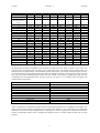
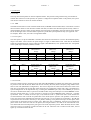
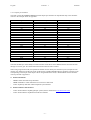
The table 6 shows the SERDES HDMP1022/1024 chipset pin allocation for IspLSI2128 setup. This should be
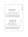
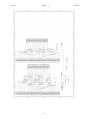
used as in the example shown in appendix 1.
Signal
D0
D1
D2
D3
D4
D5
D6
D7
D8
D9
D10
D11
D12
D13
D14
D15
D16
D17
D18
D19
CLOCK
RFD
DAV
Tx ISP pin
148
147
146
145
143
141
140
139
138
136
135
134
133
132
131
130
129
127
126
125
124
123
121
Table 6: Rx/Tx ISP pin allocation
Rx ISP pin
149
150
151
153
154
155
156
158
159
160
161
163
164
165
167
168
169
170
171
173
120
N/A
N/A
Note that the RFD pin means Ready For Data and DAV means DAta Valid. RFD should be connected to DAV
through an inverter gate. This allows data transmission when the link is locked.
When using single frame mode, the IspLSI2128 should connect directly the desired I/O pins (20 inputs and 20
outputs, user defined) to the Dx pins of the Tx/Rx chipset, and BCLKIN/BCLKOUT should be connected to the
corresponding CLOCK pin of the chipset. When using double frame mode, a MUX/DMUX scheme should be
used as presented in appendix 1.
4- Related documents
-
HDMP-1022/1024 serdes chips datasheet
HFBR-53D5/HFCT-53D5 InGaAsP Laser transceivers data sheet
Lattice Isp family data book and development system manual
5- Related software and hardware
-
Lattice Semiconductors IspDesignExpert system (free for download at www.latticesemi.com)
Lattice Semiconductors IspDownload cable and software
-5-