1
ANT+/BLE MODULE
ISP130301-ANT
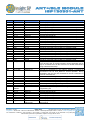
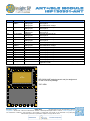
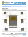
Pin
1
2
3
4
5
6
7
8
9
10
11
12
13
14
15
16
17
18
19
20
21
22
23
24
Name
P0_07
NC
P0_09
NC
P0_13
NC
P0_19
NC
P0_17
NC
P0_20
VSS
NC
VSS
NC
VSS
NC
VSS
NC
VSS
NC
VSS
VSS
OUT_MOD
Pin function
Digital I/O
Not Connected
Digital I/O
Not Connected
Digital I/O
Not Connected
Digital I/O
Not Connected
Digital I/O
Not Connected
Digital I/O
Ground
Not Connected
Ground
Not Connected
Ground
Not Connected
Ground
Not Connected
Ground
Not Connected
Ground
Ground
Module I/O
25
26
VDD_PA
OUT_ANT
PA supply
Antenna I/O
27
28
29
30
31
32
33
VSS
VSS
VCC_nRF
VSS
SWDCLK
P0_18
SWDIOnRESET
P0_16
P0_15
P0_14
P0_12
P0_10
P0_11
P0_05-AIN6
Ground
Ground
Power
Ground
Digital Output
Digital I/O
Digital I/O
34
35
36
37
38
39
40
Digital I/O
Digital I/O
Digital I/O
Digital I/O
Digital I/O
Digital I/O
Digital I/O
Analog input
Description
General purpose I/O pin
Isolated pad on application PCB for mechanical stability
General purpose I/O pin
Isolated pad on application PCB for mechanical stability
General purpose I/O pin
Isolated pad on application PCB for mechanical stability
General purpose I/O pin
Isolated pad on application PCB for mechanical stability
General purpose I/O pin
Isolated pad on application PCB for mechanical stability
General purpose I/O pin
Should be connected to ground plane on application PCB
Isolated pad on application PCB for mechanical stability
Should be connected to ground plane on application PCB
Isolated pad on application PCB for mechanical stability
Should be connected to ground plane on application PCB
Isolated pad on application PCB for mechanical stability
Should be connected to ground plane on application PCB
Isolated pad on application PCB for mechanical stability
Should be connected to ground plane on application PCB
Isolated pad on application PCB for mechanical stability
Should be connected to ground plane on application PCB
Should be connected to ground plane on application PCB
This pin is the RF I/O pin of the BLE module. It should be connected
to Pin 26 OUT_ANT for normal operation. During certification the pin
may be connected via to an RF connector for module measurement
using a Bluetooth test setup.
PA supply indicates Transmit mode (Active High)
This pin is connected to the internal antenna. It should be
connected to Pin 24 OUT_MOD for normal operation. During
certification the pin may be connected to an RF connector for
antenna measurement
Should be connected to ground plane on application PCB
Should be connected to ground plane on application PCB
Power supply (2.1 – 3.6V). VDD in nRF51822 doc.
Should be connected to ground plane on application PCB
HW debug and flash programming I/O
General purpose I/O pin
System reset (active low). Also HW debug and flash
programming I/O
General purpose I/O pin
General purpose I/O pin
General purpose I/O pin
General purpose I/O pin
General purpose I/O pin
General purpose I/O pin
General purpose I/O pin
ADC input 6
December 19, 2014
Document Ref: isp_ble_DS130301ANT_R2.docx
Page 3/15
Insight SiP – Green Side – 400 avenue Roumanille – BP 309 – 06906 Sophia-Antipolis Cedex – France – www.insightsip.com
The information contained in this document is the property of Insight SiP and should not be disclosed to any third party
without written permission. Specification subject to change without notice.