1
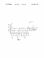
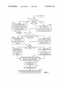
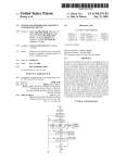
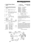
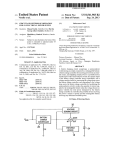
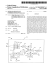
US008188717B2
(12) United States Patent
(10) Patent N0.:
(45) Date of Patent:
Schubert
(54)
ACTIVE COMMUNICATIONS BUS POWER
US 8,188,717 B2
May 29, 2012
FOREIGN PATENT DOCUMENTS
HARVESTER FOR DIFFERENTIAL SIGNAL
COMMUNICATION SYSTEM
W0
W0 2008-011894 A1
1/2008
OTHER PUBLICATIONS
(75) Inventor: Clifford Schubert, Sidney (CA)
KK Systems, Ltd., K2 RS232-RS422/485 Converter, K2-ADE
RS232-RS485 Converter With ADE, 2002 KK Systems, Ltd., Ed. 2,
(73) Assignee: Schneider Electric USA, Inc., Palatine,
IL (US)
(*)
Notice:
Jan. 11, 2002 (6 pages).
Allen-Bradley, User Manual Smart Self-Powered Serial Converter
(Cat. No. 1203-SSS) Series B FRN2.xxx, Rockwell Automation,
Publication 1203-5.15iAug. 1999 PN 193416(01) (44 pages).
International Search Report for International Application No. PCT/
US2010/059099, dated Jul. 20, 2011 (4 pages).
Written Opinion of The International Searching Authority for Inter
national Application No. PCT/US2010/059099, dated Jul. 20, 2011
Subject to any disclaimer, the term of this
patent is extended or adjusted under 35
U.S.C. 154(b) by 340 days.
(21) Appl. No.: 12/648,937
(6 pages).
(22) Filed:
Dec. 29, 2009
* cited by examiner
(65)
Prior Publication Data
US 2011/0156658A1
Primary Examiner * Ramy Ramadan
Jun. 30, 2011
(74) Attorney, Agent, or Firm * Nixon Peabody LLP
(51)
Int. Cl.
H02] 7/00
(52)
US. Cl. ..................................................... .. 320/137
(58)
Field of Classi?cation Search ................ .. 320/162,
(2006.01)
(57)
A balanced differential signal communication system having
at least tWo data lines connecting multiple nodes in series,
each node comprising a signal generator for applying signals
320/ 137
See application ?le for complete search history.
(56)
ABSTRACT
to the data lines that produce a controllable differential volt
age across the data lines; a rechargeable storage device for
References Cited
receiving electrical energy from the data lines to charge the
storage device; at least one device coupled to the storage
device for receiving electrical energy_ from the storage
device;
_
U.S. PATENT DOCUMENTS
6,363,066 B1
3/2002
Frimodig
7,034,503 B2 *
4/2006 Veselic et a1‘ ,,,,,,,,,,,,, n 320/128
and a controllable converter couplrng the data lrnes to the
7,391,299 B2
7,576,635 B2
6/2008 Bender et al.
8/2009 Bender et 31
storage device for controlling the charging and discharging of
the storage device With poWer captured from the data lines.
7,612,654 B2
2007/0168596 A1
11/2009 Bender et al.
7/2007 Hall et al.
2009/0322271 A1 *
12/2009 Zimmermann ............. .. 318/440
16 Claims, 4 Drawing Sheets
[- 1 0
12
R3
11
R1
S+
\
R2i
\
\I \
_
Power
Harvester
Device
Device
Device
A
B
N
11b
(
US. Patent
May 29, 2012
Sheet 1 of4
US 8,188,717 B2
[-10
12
R3
11
R1
8+
R4
\ \
R2
(
Power
Harvester
S_
_
Device
Device
Device
_
A
B
N
11a
11b
FIG. 1
110
US. Patent
May 29, 2012
US 8,188,717 B2
Sheet 3 0f 4
101
ls
storage power
enough to start
102\
microcontroller?
f 104
DC-DC uses reference voltage to
determine loading and operate as single
unit load. Captures energy from bias
voltage/messages until enough power to
Start microcontroller.
If at any time power goes below
threshold, power down micro and restart.
start up microcontroller
Micro now controls variable load.
103
105
Are
there previously stored
106 \
network setting?
r107
Load harvesting settings and
.
.
Turn on bus driver and voltage
resume operation.
.
.
.
.
sense, listen for messages from
Start up radio. Continue to adjust
.
.
.
different present device bus
harvesting parameters as
.
.
drivers from other devices
needed.
108
essages
1 O9 \
3
1 10
Heard?
N
f
Analyze messages to
Try sending message and listen for
determine network type
and other devices on
bus. Record signal
response.
Determine if any other devices
and their characteristics
strength.
(protocol, signal strength, etc)
f1 1 1
Analysis provides: statistics on devices with most
>
powerful transmit power, longest message
<—
response, max load harvester can apply.
+
/1 12
Adjust loading to provide
maximum power
+
/-1 13
Save network settings
+
I
f- 1 1 4
Query periodically to keep power reserves up. Start up radio.
Continue to adjust harvesting parameters as needed.
FIG. 3
US. Patent
May 29, 2012
Sheet 4 of4
US 8,188,717 B2
201
Stable
power supply
available?
K
202
Power up &
configure radio
Wait for data
from radio
204
Is the
message for the
Harvester
bus or the
arvester?
f
205
207
\
Send data out bus,
Analyze message (time sync,
wait for reply
polling schedule, etc)
i K206 20s\Apply changes, send
l acknowledge
—
Send data out
through radio if required. Start
radio
.
scheduled polling, etc.
FIG. 4
—
US 8,188,717 B2
1
2
ACTIVE COMMUNICATIONS BUS POWER
HARVESTER FOR DIFFERENTIAL SIGNAL
COMMUNICATION SYSTEM
inputs receiving the control signal produced by the microcon
troller; and a source of a ?xed reference voltage coupled to the
FIELD OF THE INVENTION
may be programmed to send messages via the data lines to
other nodes coupled to the data lines to cause the other nodes
to respond to the messages via the data lines, and the converter
other of the inputs to the multiplexer. The microcontroller
The present invention relates generally to supplying poWer
captures poWer from the responses for recharging the storage
device.
to devices coupled to a differential signal communication
system by harvesting electrical poWer from data lines of the
communication system.
One embodiment includes a sensor coupled to the data
lines for sensing the voltage differential betWeen the data
lines and supplying a signal representing the voltage differ
BACKGROUND
ential to the microcontroller, and a microcontroller is pro
Differential signal communication systems are in Wide
spreaduse. For example, RS-485 is a Well knoWn serial digital
communication system that uses balanced differential signals
for communicating With computers and other devices.
RS-485 alloWs multiple devices to communicate at half-du
tial to determine a load that can be imposed on the data lines
grammed to use the signal representing the voltage differen
plex on a single pair of Wires, plus a ground Wire, over long
distances. Both the length of the netWork and the number of
nodes can easily be extended using a variety of different
repeater products that are readily available. The properties of
Without interfering With communications on the data lines.
The converter is preferably controllable to vary the load that
the converter imposes on the data lines, so that the load does
not interface With communicating via the data lines.
20
The invention may best be understood by reference to the
differential signals provide high noise immunity and long
distance capabilities.
RS-485 is the most versatile communication standard in
folloWing description taken in conjunction With the accom
panying draWings, in Which:
25
the standard series de?ned by the EIA, as it performs Well for
FIG. 1 is a block diagram of an RS-485 communication
system that includes multiple nodes and a poWer harvesting
device for harvesting electrical poWer from the data lines of
the bus.
connecting data terminal equipment (DTE) directly Without
the need of modems, for connecting several DTE’s in a net
Work structure, for communicating over long distances, and
for communicating at fast communication rates. RS-485 is
currently a Widely used communication interface in data
BRIEF DESCRIPTION OF THE DRAWINGS
30
FIG. 2 is a block diagram of one of the nodes in the system
of FIG. 1.
FIG. 3 is a How chart of a program executed by the micro
acquisition and control applications Where multiple nodes
controller in the node of FIG. 2 to control the harvesting of
communicate With each other. RS-485 signals are ?oating
electrical poWer from the bus.
FIG. 4 is a How chart of a program executed by the micro
controller in the node of FIG. 2 to control radio/bus messag
1ng.
With each signal being transmitted over a S+ line and a S
line. The RS-485 receiver compares the voltage difference
betWeen the tWo lines, rather than the absolute voltage level
35
on a single line.
RS-485 interfaces are often preferred for data acquisition
and control applications because RS-485 is capable of inter
netWorking multiple transmitters and receivers in the same
network. High-resistance RS-485 inputs alloW a large num
DETAILED DESCRIPTION
40
Although the invention Will be described in connection
With certain preferred embodiments, it Will be understood that
the invention is not limited to those particular embodiments.
On the contrary, the invention is intended to cover all alter
ber of nodes to be used, and RS-485 repeaters can be used to
increase the number of nodes even more.
natives, modi?cations, and equivalent arrangements as may
BRIEF SUMMARY
45
be included Within the spirit and scope of the invention as
de?ned by the appended claims.
The present disclosure provides a balanced differential
signal communication system having at least tWo data lines
gram of an RS-485 communication system that includes a
connecting multiple nodes in series, each node comprising a
signal generator for applying signals to the data lines that
50 and multiple nodes formed by devices 11a, 11b . . . 11n
Turning to the draWings, FIG. 1 is a functional block dia
differential bus 10 is formed by a pair of data lines S+ and S—,
produce a controllable differential voltage across the data
coupled to the bus 1 0 at different points along the length of the
lines; a rechargeable storage device for receiving electrical
energy from the data lines to charge the storage device; at
bus. An RS-485 communication channel can be shared by
least one device coupled to the storage device for receiving
electrical energy from the storage device; and a controllable
converter coupling the data lines to the storage device for
multiple receivers and multiple senders. In the illustrative
embodiment, the bus 10 is terminated by resistances R1 and
55
controlling the charging of the storage device With poWer
captured from the data lines.
One implementation includes a microcontroller coupled to
the controllable converter and producing a control signal that
affects the amount of poWer captured from the data lines by
the converter; a multiplexer coupled betWeen the microcon
troller and the converter and having a pair of input terminals
for receiving a pair of input signals, an output terminal, and a
control input for receiving a control signal from the micro
controller for selecting Which input signals are included in the
output signal produced at the output terminal, one of the
R2 at opposite ends, and a bias voltage is supplied to one end
of the bus from a source 12 through voltage divider formed by
a pair of resistors R3 and R4 in combination With the termi
nating resistor R1. For high bit rates and long Wiring runs,
termination resistances are necessary on both ends of the bus
60
10 to eliminate re?ections, but not at drop points along the
bus. Highbit rates are possible because the transitionbetWeen
logical 0 and logical l is only a feW hundred millivolts, and
currently available RS-485 drivers can achieve bit rates of at
least 35 mbps.
65
Although FIG. 1 illustrates an RS-485 tWo-Wire multi-drop
bus, it Will be understood that an RS-485 netWork can also be
connected in a four-Wire mode, using four data Wires and an
US 8,188,717 B2
3
4
additional signal ground Wire. In a four-Wire network, one
is a rechargeable battery, it may be installed pre-charged to
reduce the initial charge and discovery time, or it may be
node is a master node and all others are slave nodes. The
network is connected so that the master node communicates
initially charged by some other means such as a USB plug-in
to all slave nodes, and all slave nodes communicate only With
to a computer.
the master node. Since the slave nodes never listen to another
slave response to the master, a slave node cannot reply incor
rectly to another slave node. RS-422 systems are also use
To control the charging of the energy storage device 34, the
microcontroller produces control signals for a multiplexer 35
that also receives a reference voltage form a reference voltage
source 36. The multiplexer 35 selects one of its tWo inputs,
from the microcontroller 22 and the reference voltage source
36, for application to the converter 33. The selection is con
trolled by a “select” signal generated on output line 2211 from
the microcontroller 22 and applied to the select input of the
multiplexer 35, Which determines Which of the tWo multi
balanced differential signals, using a dedicated pair of Wires
for each signal, a transmit pair, a receive pair and an additional
pair for each handshake/ control signal used (if required). In a
“tWo-Wire” netWork the transmitter and receiver of each
device are connected to a tWisted pair. “Four-Wire” netWorks
have one master port With the transmitter connected to each of
the “slave” receivers on one tWisted pair. The “slave” trans
plexer inputs is supplied to the converter 33. It Will be under
stood that either a digital or analog multiplexer may be used,
depending on the type of control desired for the converter 33.
mitters are all connected to the “master” receiver on a second
tWisted pair. In either con?guration, devices are addressable,
alloWing independent communications With each node.
FIG. 2 is a more detailed illustration of one of the node
devices 11, Which includes a communication and bus loading
control 20 and an energy capture system 30, both of Which are
coupled to the tWo data lines 8+ and S- of the bus 10. As is
Well knoWn, the data lines 8+ and S- are preferably in the
form of a tWisted pair, to provide noise immunity. The energy
capture system 12 supplies electrical poWer to a poWer supply
40 that poWers the communication and bus loading control
20
other devices on the bus. By controlling the converter, the
system is able to vary the load it puts on the bus 10 to capture
more or less poWer, While ensuring that the load does not
interfere With communications. The converter may be con
25
11.
Within the communication and bus loading control 20, an
RS-485 bus driver 21 sends signals to, and receives signals
from, the data lines 8+ and S- of the bus 10. The driver 21
delivers received signals to a microcontroller 22, and receives
signals from the microcontroller 22 for delivery to the bus 10.
Only one device can drive the data lines at a time, so the
drivers at the various nodes must be put into a high-imped
30
35
storage device 34 capture a small amount of poWer from the
biasing circuit for the bus 10. The converter 33 varies its load
to draW as much poWer as possible from the bus biasing
standard. Any communications that occur on the bus 10 alloW
the converter 33 to charge the storage device 34 faster than
just the biasing voltage, and those communications can also
be used to identify the type of netWork or protocol being used,
as described in more detail beloW.
40
After the storage device 34 has accumulated enough
energy to enable the microcontroller 22 and the driver 21 to
generate a request, they transmit a harmless request to the
other nodes on the bus 10, such as a Modbus read or identify
ance tri-state Within a feW microseconds after data has been
sent, so it is not necessary to have delays betWeen data packets
on the RS-485 bus. These tristate capabilities of RS-485
nodes alloW a single pair of Wires to share transmit and
trolled to change not only the poWer captured from the bus 1 0,
but also the impedance it presents to the bus to improve
communication and/ or the poWer harvesting capabilities.
Upon connection to the bus 10, the converter 33 and the
circuit Without exceeding the speci?cation of the communi
cations system or dropping the biasing voltage beloW the
appropriate threshold for the applicable communications
ance mode (tri-state) When they are not in use. An RS-485
driver is typically enabled and disabled by an RTS control
signal from an asynchronous serial port. Setting the RTS line
to a high (logic 1) state enables the driver, While setting the
RTS line to a loW (logic 0) state puts the driver into a tristate
condition that in effect disconnects the driver from the bus,
alloWing other nodes to transmit over the same pair of data
lines. The RS-485 driver typically returns to its high imped
This control of the converter 33 enables the system 30 to
capture small amounts of energy from the biasing voltage on
the bus 10, or to capture larger amounts of energy from data
signals on the bus When the data lines 8+ and S- are driven by
45
receive signals for half-duplex communications.
request. The microcontroller may identify the desired type of
communication automatically by monitoring traf?c on the
bus 10, or the microcontroller may have been pre-con?gured
The microcontroller 22 also receives the output of an
for a certain setting. If there is no response to a request
operational ampli?er 23 that has tWo inputs coupled to the
generated by the microcontroller 22 and the driver 21, the
converter 33 continues charging the storage device 34 from
tWo data lines 8+ and 8-, so that the output of the ampli?er 23
represents the difference betWeen the voltage levels on the
tWo data lines 8+ and S—. The microcontroller 22 also
50
receives inputs from a real time clock 24 and a radio trans
the bias voltage While the microcontroller 22 continues to
generate different types of messages or targets different nodes
until a response is received.
ceiver 25, and delivers control signals to the energy capture
After a response is received, the poWer-harvesting system
system 30, as Will be discussed in more detail beloW. The
transceiver 25 is typically a generic loW poWer radio trans
ceiver, such as a ZigBee radio, or the transceiver may be
has a better source of poWer and can begin issuing additional
requests to detect other protocols or devices on the netWork.
For example, certain nodes on the bus 10 may have stronger
replaced With a signal/protocol converter.
The energy capture system 30 includes a recti?er 31 having
a pair of inputs coupled to the tWo data lines 8+ and S—,
producing a recti?ed output that is smoothed by a ?lter 32 and
55
drivers, Which can be detected by varying the load on the
netWork While listening for a response, or certain nodes may
60
then supplied as the DC input to a controllable DC-to-DC
converter 33. The DC output of the converter 33 is supplied to
an energy storage device 34, such as a rechargeable battery or
an ultra capacitor. The output of the storage device 34 is
connected to the poWer supply 40 that supplies poWer to the
respond faster or support other commands that produce
longer responses and therefore supply more poWer for each
request. The microcontroller may be programmed to look for
the option that Will provide the most poWer for charging the
storage device 34, both in terms of the device’s driving capa
communication and bus loading control 20, including the
bilities and the ratio of poWer received to poWer required to
transmit.
In the illustrative example With the radio 25, the microcon
microcontroller 22 and the radio 25. When the storage device
troller 22 can turn on the radio 25 and thus begin Wireless
65
US 8,188,717 B2
5
6
communications after a stable source of energy has been
response, the maximum load the harvester can apply to the
obtained and su?icient energy has been stored. Other nodes
on the bus 10 can be polled as needed to maintain the required
poWer.
When the illustrative device is acting as a bridge or con
verter betWeen a radio netWork and a Wired communications
bus 10 Without adversely affecting communications, etc.
From step 11, the system advances to step 112 to adjust the
loading on the bus 10 to provide maximum poWer to recharge
the storage device 34, and then those netWork settings are
saved at step 113. Then step 114 queries the netWork settings
bus, incoming requests can be buffered While poWer is being
periodically and adjusts the poWer-harvesting parameters as
harvested from the Wired bus. Then a message can be trans
needed to maintain a maximum poWer reserve. It Will be
mitted from the Wireless network, and any response Will be
understood that the loading on the bus is adjusted by the
DC-to-DC converter 33 in response to the output signal
received by the converter from the multiplexer 35, Which in
turn is controlled by the control signal applied to the select
input of the multiplexer 35 by the microcontroller 22.
forWarded back onto the radio netWork. The radio 25 or the
entire device may be designed to go into a loW poWer “sleep”
state and only poWer up When traf?c is received from the
Wired communications bus, or in response to a periodic radio
timer.
FIG. 4 is a How chart of a routine executed by the micro
controller 22 to control messaging operations via the radio 25
and the bus 10. The radio 25, Which can Wait to be triggered by
FIG. 3 is a How chart of a poWer-up sequence for the poWer
harvester illustrated in FIG. 2. Step 101 determines Whether
the energy storage device 34 has accumulated enough poWer
to start the microcontroller 22, and if the ansWer is negative,
step 102 indicates that the DC-to-DC converter 33 uses the
?xed reference voltage from source 36 to determine the load
ing on the bus 10. That is, the converter 33 operates as a single
another device or can query a central device on poWer up,
20
The routine in FIG. 4 begins at step 201, Which determines
unit load, capturing energy from the bias voltage and any
messages on the data lines S+ and S- until enough poWer is
accumulated in the storage device 34 to start up the micro
controller 22.
When the response at step 101 is af?rmative, the micro
controller 22 is started at step 104 so that the balance of the
steps in FIG. 3 can be executed by the microcontroller. If at
any time the poWer available from the storage device 34 drops
beloW a preselected threshold, the microcontroller 22 is poW
ered doWn and re-started When the accumulated poWer again
Whether a stable poWer supply is available, based on stored
data relating to poWer supplied to the microcontroller from
25
30
35
synchronization, polling schedule, etc. Step 208 then applies
required, starts scheduling polling, etc.
While particular embodiments and applications of the
40
the netWork settings periodically and adjusts the poWer-har
45
When step 105 yields a negative response, indicating that
there are no previously stored netWork settings, the system
advances to step 107 to turn on the bus driver 21, to turn on the
voltage differential-sensing ampli?er 23, and to listen for
messages. The system then advances to step 108 to listen for
messages. When a message is detected, step 108 produces an
af?rmative response, Which advances the system to step 109
Which analyZes the message to collect data from the message,
such as netWork type, other devices on the bus and signal
strength. The collected data is then analyZed at step 111 to
determine desired statistics such as the identity of devices
50
spirit and scope of the invention as de?ned in the appended
claims.
The invention claimed is:
1. A balanced differential signal communication system
having at least tWo data lines connecting multiple nodes in
series, each node comprising a signal generator for applying
signals to said data lines that produce a controllable differen
tial voltage across said data lines, a receiver coupled to said
55
data lines for detecting said differential voltage, a recharge
able storage device coupled to said data lines for receiving
electrical energy from said data lines to charge said storage
device, at least one device coupled to said storage device for
receiving electrical energy from said storage device, and a
controllable converter coupling said data lines to said storage
device for controlling the charging of said storage device With
having the most transmit poWer, the longest message
response, the maximum load the harvester can apply to the
bus 10 Without adversely affecting communications, etc.
When no message is detected, step 108 yields a negative
present invention have been illustrated and described, it is to
be understood that the invention is not limited to the precise
construction and compositions disclosed herein and that vari
ous modi?cations, changes, and variations may be apparent
from the foregoing descriptions Without departing from the
vesting parameters as needed to maintain a maximum poWer
reserve.
determines Whether the radio message is for the bus 10 or the
poWer harvester. If the message is for the bus, the data is sent
out on the bus 10 at step 205, after being reformatted by the
microcontroller 22 if necessary, and is then sent out on the
radio 25 at step 206. If step 204 determines that the radio
message is for the poWer harvester, the routine advances to
step 207 to analyZe the message for information such as time
any changes, sends an acknowledgment through the radio if
determines Whether there are any previously stored netWork
settings. If step 105 yields an af?rmative ansWer, the system
proceeds to step 106 to load any settings for the poWer har
vester settings and resume operation, including turning on the
radio 25. The system then advances to step 114, Which queries
the poWer supply 40 over a selected time interval. This step
repeats until it produces an af?rmative response, Which
advances the system to step 202 to poWer up and con?gure the
radio 25. Step 203 then Waits for data from the radio 25, and
advances to step 204 When such data is received. Step 204
rises above that threshold. After the microcontroller 22 has
been started, the microcontroller 22 controls the variable load
imposed on the bus 10 by the DC-to-DC converter 33, via the
control signal applied to the select input of the multiplexer 35
by the microcontroller.
From step 104, the system advances to step 105, Which
serves to synchroniZe multiple poWer harvesters and to relay
messages betWeen the bus 10 and another location, either on
request or as part of a scheduled operation.
60
response, the system advances to step 110 to transmit a mes
poWer captured from said data lines, Wherein said signal
generator generates signals for transmission to other nodes
coupled to said data lines to stimulate said other nodes to
sage via the bus driver 21 and then listen for a response. Any
response is used to collect the same type of data collected at
111 to determine desired statistics such as the identity of
generate signals for transmission via said data lines, to pro
vide additional poWer to be captured by said converter from
said data lines.
2. The balanced differential signal communication system
devices having the most transmit poWer, the longest message
node of claim 1 Which includes a microcontroller coupled to
step 109, namely, netWork type, other devices on the bus
signal strength, etc. The collected data is then analyZed at step
65
US 8,188,717 B2
8
7
12. The balanced differential signal communication sys
said controllable converter and producing a control signal that
affects the amount of poWer captured from said data lines by
tem node of claim 2 Which includes
said converter.
3. The balanced differential signal communication system
a multiplexer coupled betWeen said microcontroller and
said converter and having a pair of input terminals for
of claim 1 in Which said controllable converter imposes a
DC-to-DC load on said data lines at a default level, and Which
receiving a pair of input signals, an output terminal, and
includes control circuitry for overriding said default-level
microcontroller for selecting Which input signals are
included in the output signal produced at said output
terminal, one of said inputs receiving said control signal
a control input for receiving a control signal from said
load to increase the DC-to-DC load on said data lines to
increase the rate of charging said storage device.
4. The balanced differential signal communication system
node of claim 1 Which includes a bias voltage source coupled
produced by said microcontroller, and
a source of a ?xed reference voltage coupled to the other of
to said data lines for applying a bias voltage across said data
lines.
said inputs to said multiplexer.
13. A method of harvesting electrical poWer from a bal
5. The balanced differential signal communication system
anced differential signal communication system having at
node of claim 1 Which includes a voltage source and bias
least tWo data lines connecting multiple nodes that include a
resistors connected across said data lines to maintain a mini
mum bias current How in said data lines for noise suppression.
signal generator for applying signals to said data lines to
6. The balanced differential signal communication system
node of claim 1 in Which said controllable differential voltage
produce a controllable differential voltage across said data
lines, and a receiver coupled to said data lines for detecting
has tWo different levels, representing the tWo states of a binary
signal transmitted via said communication line.
said differential voltage, said method comprising coupling a
20
7. The balanced differential signal communication system
node of claim 1 in Which said rechargeable storage device is
rechargeable storage device to said data lines through a con
trollable converter that charges said storage device With elec
trical energy captured from said data lines, coupling at least
a rechargeable battery or a capacitor.
one device to said storage device for receiving electrical
8. The balanced differential signal communication system
node of claim 2 in Which said microcontroller is programmed
energy from said storage device, and generating signals for
25
transmission to other nodes coupled to said data lines to
30
stimulate said other nodes to generate signals for transmis
sion via said data lines, to provide additional poWer to be
captured by said converter from said data lines.
14. The method of claim 13 Which includes rectifying
non-DC energy removed from said data lines, said control
to send messages via said data lines to other nodes coupled to
said data lines to cause said other nodes to respond to said
messages via said data lines, said converter capturing poWer
from said responses for recharging said storage device.
9. The balanced differential signal communication system
node of claim 1 in Which said converter is controllable to vary
the load that said converter imposes on said data lines, so that
said load does not interface With communicating via said data
lines.
10. The balanced differential signal communication sys
lable converter imposes a DC-to-DC load on said data lines,
and controlling said DC-to-DC load to adjust the rate of
charging said storage device Without interfering With com
munications on said data lines.
35
tem node of claim 2 Which includes a sensor coupled to said
data lines for sensing the voltage differential betWeen said
data lines and supplying a signal representing said voltage
charging said storage device.
differential to said microcontroller, and said microcontroller
is programmed to use said signal representing said voltage
40
differential to determine a load that can be imposed on said
data lines Without interfering With communications on said
data lines.
11. The balanced differential signal communication sys
tem node of claim 1 in Which said load imposed by said
controllable converter on said data lines is an adjustable resis
tive or reactive load.
15. The method of claim 14 in Which said DC-to-DC load
is imposed on said data lines at a default level, and Which
includes overriding said default-level load to increase the
DC-to-DC load on said data lines to increase the rate of
16. The method of claim 13 Which includes sending mes
sages via said data lines to other nodes coupled to said data
lines to cause said other nodes to respond to said messages via
said data lines, said converter capturing poWer from said
responses for recharging said storage device.
45