1
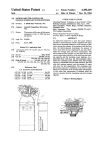
US008541983B2
(12) United States Patent
Veselic et al.
(54)
CIRCUIT AND METHOD OF OPERATION
FOR AN ELECTRICAL POWER SUPPLY
US 8,541,983 B2
(10) Patent N0.:
(45) Date of Patent:
(56)
Sep. 24, 2013
References Cited
U.S. PATENT DOCUMENTS
(75) Inventors: Dusan Veselic, Oakville (CA); Martin
3,775,659 A
George Albert Guthrie, Moffat (CA)
Notice:
Subject to any disclaimer, the term of this
patent is extended or adjusted under 35
2/1984 Banks et al.
(Continued)
(73) Assignee: BlackBerry Limited, Waterloo, Ontario
(CA)
(*)
ll/l973 Carlsen, II
4,433,251 A
FOREIGN PATENT DOCUMENTS
DE
201 16 332
WO PCT/CA2004/000249
1/2002
9/2004
OTHER PUBLICATIONS
U.S.C. 154(b) by 271 days.
“Notice Requesting Submission of Opinion,” issued in correspond
ing Korean Patent Application No. 10-2005-7015376, dated Oct. 27,
(21) App1.No.: 13/175,541
2010, pp. 1-6.
(22)
Filed:
Charging Big Supercaps, Portable Design, p. 26, Mar. 1997.
Jul. 1, 2011
(65)
US 2011/0260680 A1
Oct. 27, 2011
Related U.S. Application Data
(63)
Continuation of application No. 13/028,361, ?led on
Feb. 16, 2011, now Pat. No. 7,999,514, which is a
continuation of application No. 12/860,591, ?led on
Aug. 20, 2010, now Pat. No. 7,906,940, which is a
continuation of application No. 10/372,180, ?led on
Feb. 21, 2003, now Pat. No. 7,791,319.
(51)
Int. Cl.
H02] 7/00
H02] 7/16
G01R 19/12
(52)
(2006.01)
(2006.01)
(2006.01)
Primary Examiner * Edward Tso
Assistant Examiner * Alexis Boateng
(74) Attorney, Agent, or Firm * Finnegan, Henderson,
Farabow, Garrett & Dunner, LLP
(57)
ABSTRACT
A battery charging circuit comprising: a semiconductor
switch having an output connected to a rechargeable battery;
a battery charge controller for receiving power from an exter
nal source, and supplying output power to a portable device
and the input of the semiconductor switch, the current output
of the battery charge controller being controllable; and a
voltage sensing circuit for: measuring the voltage drop across
the battery charge controller; and responding to the voltage
drop across the battery charge controller by modulating the
U.S. Cl.
semiconductor switch to reduce the quantity of current sup
USPC ......... .. 320/134; 320/156; 320/132; 320/159;
plied to the rechargeable battery when the voltage drop is too
great; whereby the total power dissipated by the battery
charge controller is controlled, the portable device receiving
the power it needs to operate and the rechargeable battery
320/160; 320/114; 307/32; 307/152
(58)
(Continued)
Prior Publication Data
Field of Classi?cation Search
USPC
............... .. 320/112,113,114,115,152,157,
320/155,134,132,156,165,158,159,160;
307/32, 34, 38, 39, 152, 159
See application ?le for complete search history.
receiving any additional available power.
26 Claims, 8 Drawing Sheets
30
/
VOLTAGE
SENSING CIRCUIT
VBUS
BATTERY
CHARGE
CONTROLLER
GATE
@DOUT
IN
/
20
R1
PORTABLE
DEVICE
:-\24
US 8,541,983 B2
Page 2
References Cited
4,510,431
4,755,816
5,173,855
5,179,335
5,229,649
5,272,475
5,444,378
U'S' PATENT DOCUMENTS
A
4/1985 Winkler
A
7/1988 DeLuca
A
12/1992 Nielsen et al.
A
1/1993 Nor
A
A
7/1993 Nielsen et al.
12/1993 Eaton et al.
8/1995 Rogers
A
6,191,552 B1 *
6,211,649
6,252,375
6,300,744
6,346,794
6,362,610
6,373,229
6,437,541
6,437,543
6,498,458
6,801,967
B1
B1
B1
B1
B1
B1
B1
B1
B1
B2
6,936,936 B2*
2/2001
4/2001
6/2001
10/2001
2/2002
3/2002
4/2002
8/2002
8/2002
12/2002
10/2004
K3168 61211. ................. .. 320/112
Matsuda
Richter et a1.
Shum
Odaohhara
Yang
Slusky
Sakurai
Oler et a1.
Chen
Nakamura etal.
5,631,503 A
5/1997 Ciof?
5,638,540 A
6/1997 Aldous
2001/0004310 A1
6/2001 Kono
5,651,057 A
5,721,481 A
7/1997 Blood et al.
2/1998 Narita et al.
2001/0015635 A1*
2002/0079866 A1*
8/2001 Leppo et a1. ................ .. 320/116
6/2002 Odaohhara ................. .. 320/150
5,734,254 A
5,769,877 A
3/1998 Stephens
6/1998 BaffefaS,Sf~
2003/0052547 A1
2003/0076138 A1
3/2003 Fischer et a1.
4/2003 Hwang
5,804,894 A
9/1998 Leeson et al.
2003/0146736 A1*
8/2003
5,814,972 A
5,850,113 A
9/1998 Shimada et al.
12/1998 Weimer et al.
2003/0155892 A1
2003/0204708 A1
8/2005 Fischer et a1. .............. .. 307/151
Kosuda et al. .............. .. 320/132
8/2003 Poletti
10/2003 Hulme et al.
5,898,290 A *
4/1999 Beard et a1. ................. .. 307/150
2004/0042138 A1
3/2004
Saito etal.
5,898,293 A *
4/1999
2004/0100226 A1*
5/2004
Sakurai ....................... .. 320/136
5,926,006
5,939,860
6,100,664
6,104,162
6,104,759
6,118,254
6,130,518
A
A
A
A
A
A
A
7/1999
8/ 1999
8/2000
8/2()()()
8/2000
90000
10/2000
*
Tamaiet al. ................ .. 320/136
Burroughs et al.
William
Oglesbee et a1.
Sajnsbmy et 31,
C?fknef et al~
Faulk
Gabehart et a1.
'
OTHER PUBLICATIONS
Examiner’s report on European Patent Application No. 047129796
mailed Dec. 15, 2010, from the EPO (4 pgs.).
Supercapacitor: User’s Manual, vol. 2 (Japan, Tokin Corp., date
unknown)
.
231233552; 2
@5888
etal' """"""""" " 320/132
6,157,173 A *
12/2000 Bamnowski et al‘ ““““ H 320/152
6,172,478 B1
1/2001 Leppo et a1.
6,184,652 B1
2/2001 Yang
China Of?ce Action issued Nov. 17, 2011, in Application No.
2004800047271 and Engllsh Translat1on (4 pages).
* cited by examiner
US. Patent
Sep. 24, 2013
US 8,541,983 B2
Sheet 1 0f 8
18
/
PORTABLE
DEVKJE
PC
14.
BATTERY CHARGE
USB CARD
CONYROLLER
\
/
12
FIG- 2
(Pn'or Art)
20
US. Patent
Sep. 24, 2013
US 8,541,983 B2
Sheet 2 0f 8
18
FIG. 3
/
PORTABLE
DEVICE
PC
11
BATTERY
USB CARD
CHARGE
CONTROLLER
\
20
FIG. 4
30
VOLTAGE
sewsme cchun
BATTERY
VBus
CHARGE
CONTROLLER
GATE
@D OUT
|N
/
20
PORTABLE
R1
DEVICE
\
18
-
US. Patent
Sep.24,2013
US 8,541,983 B2
Sheet30f8
mo<IwE >
m2; .mvam
US. Patent
Sep.24,2013
US 8,541,983 B2
Sheet40f8
41
qw/Wv
8
N@
mamA
A
5
W"?Sam+y;
w.UE
H/3E3wc?éoasnz“$w5sm2ét8o
J_
6
§
2
8w3m>
mm
F
M
[email protected]
8
5
US. Patent
Sep. 24, 2013
US 8,541,983 B2
Sheet 5 0f 8
$1250
OE4h>
26
"a
5
zF
E
QUE
<
LI“
0mzw;N
52"w
25m ms“.,w0.
l.“
“We
M
me6w?5:2%sz020NF
M£88
D
.m
minmy? H
. 96Q626as965
“32w
XqI
N"t:wxgmmNEE__k?w
H
vv
m
?
P
FVL
l_.
mg3
%
W
38522V5%8M
2 8>Emma96w
$02EI
x?2:.§v52oz9v626.2
EHESu]g
m2250>25<35m$5
_m
M
i
Q.
w
LAIT
H
02026‘ ‘
.52<<<_.<|m>
VJ;- oz50%
52%v
ea26
5-26
US. Patent
Sep. 24, 2013
Sheet 8 0f8
90 '\
CONNECTING BATTERY CHARGE
CONTROLLER TO EXTERNAL POWER SUPPLY
92
CONNECTING OUTPUT OF BATTERY CHARGE
T
\
CONTROLLER TO PORTABLE DEVICE AND A
SEMICONDUCTOR IN PARALLEL
I
94\
CONNECTING OUTPUT OF SEMICONDUCTOR
TO RECHARGEABLE BATTERY
I
96 \
CONTROLLING CURRENT OUTPUT LEVEL
OF BATTERY CHARGE CONTROLLER
I
98 /
MEASURING VOLTAGE DROP ACROSS
BATTERY CHARGE CONTROLLER
I
100/
RESPONDING TO VOLTAGE DROP ACROSS
BATTERY CHARGE CONTROLLER BY
MODULATING SEMICONDUCTOR SWITCH
TO REDUCE CURRENT TO RECHARGEABLE
BATTERY WHEN VOLTAGE DROP IS TOO GREAT
FIG. 8
US 8,541,983 B2
US 8,541,983 B2
1
2
Hence, lithium batteries are almost invariably used with
CIRCUIT AND METHOD OF OPERATION
FOR AN ELECTRICAL POWER SUPPLY
battery charge controllers designed to their particular charg
ing parameters.
application Ser. No. 12/860,591, ?led Aug. 20, 2010, (now
Unfortunately, mo st battery charge controllers are
designed to draw from a high capacity power supply with a
steady voltage that will not sag appreciably under its current
U.S. Pat. No. 7,906,940), which is a continuation of Us.
demands. This is a problem when one attempts to use a power
This is a continuation of Us. application Ser. No. 13/028,
361, ?led Feb. 16, 2011, which is a continuation of Us.
application Ser. No. 10/372,180, ?led Feb. 21, 2003, (now
supply with limited capacity. Some computer data buses such
U.S. Pat. No. 7,791,319), all ofwhich are incorporated herein
as USB (universal serial bus) buses can be used to provide
power to external devices, but while such power supplies are
by reference.
This invention relates in general to battery chargers, and
more speci?cally to a method and apparatus for charging a
very convenient, they have limited capacity.
The majority of personal computers (PCs) and laptop com
battery in a portable communication device from a variety of
puters available today, are provided with one or more USB
power sources, including limited capacity sources such as an
integral power node of a computer data bus. One such com
ports as standard components. USB ports are designed to
puter data bus would be a USB (universal serial bus) port.
megabits per second, support PnP (Plug and Play) installation
support data communication at speeds of 12 megabits and 1.5
software, and support hot plugging (i.e. devices can be con
nected and disconnected while the PC is running). Thus, USB
BACKGROUND OF THE INVENTION
20
With the current computing and information revolution,
portable electronic devices such as cellular telephones, per
ports are often used as interfaces to connect keyboards,
mouses, game controllers, printers and scanners to PCs.
As well, USB ports are operable to supply limited power to
sonal digital assistants (PDAs), digital pagers and wireless
connected external devices. The standard USB speci?cation
email devices, are becoming very common. These portable
requires that “high-power” USB ports be operable to provide
devices are typically powered by internal batteries which
must be recharged periodically by an external power source,
25
using a battery charger. Battery chargers generally receive
cation for “low-power” USB ports requires a supply voltage
power from a standard AC electrical outlet and convert the AC
of 4.40-5.25 VDC and current of 100 mA (referred to as “one
power into a low DC voltage for recharging a battery.
The battery chargers of these portable devices also gener
ally employ a “battery charge controller” to manage the
30
unit”).
USB ports would seem to be a very logical choice as a
power supply for portable devices for a number of reasons. To
charging of the battery. Such battery charge controllers offer
being with, USB ports supply a low DC voltage supply which
is often very close to, or just above, the voltage of the battery
functionality such as:
regulating the voltage and current levels to the recharge
able battery;
a supply voltage of 4.75-5.25 VDC and a supply current of at
least 500 mA (often referred to as “?ve units”). The speci?
35
being charged (many portable devices having battery voltages
fully charged, be charged and re-charged many times, and be
in the range of 2.5-4.5 VDC). As well, many portable devices
may be operable to upload and download data or software, to
and from a personal computer or a laptop computer (often
referred to as “syncing”). Thus, many portable devices are
supplied with docking cradles as shown in the system dia
gram of FIG. 1. This is quite a straightforward system, as the
docking cradle 10 is connected to a USB port 12 of a personal
computer (PC) 14, via a simple USB cable and connectors 16.
The portable device 18 need only be set down in the docking
cradle 10 and an electronic connection to the PC 14, is made.
If the USB port 12 has suf?cient power, it makes much
safely operated. This charging algorithm generally proceeds
more sense to use the USB port 12 to supply charging power
as follows:
to the portable device 18, rather than using a separate AC
providing status signals to the main processor of the por
table device, or operating one or more status LEDs (light
emitting diodes):
providing protection circuits such as overcurrent, under
voltage, reverse polarity and overtemperature protec
40
tion; and
shutting themselves off when the charging source has been
removed, to minimize battery drain.
Lithium ion battery packs, for example, must be charged
according to a relatively strict algorithm so that they can be
45
charger. For example:
1. at the ?rst stage, any severe undervoltage or deep dis
charge conditions are addressed. During this pre-charg
ing stage, the battery voltage is gently brought up from a
50
1. a USB power supply will have less electrical noise than an
AC charger, unless the AC charger incorporates large DC
capacitors or inductors;
very low or dead state, usually at a rate of 1/10 of the
regular charge current;
2. an AC charger requires either a heavy transformer or an
level (say, 4.2 VDC). At this point the battery will only
expensive switching power supply, neither of which would
be required if USB power is used;
3. in the USB power supply implementation, the cable and
be at 40 to 70% of full capacity; and then
3. charging of the battery continues at a constant voltage
connectors 16 used to connect the docking cradle 10 to the
PC 14 could be used to carry both power and data, so no
2. next, the battery is charged at a constant current level,
until the voltage across the battery reaches its design
level (again, say 4.2 VDC) until it is fully charged. In this
mode, the current drawn by the battery will drop over
time. When the charge current has dropped to 10% of the
55
60
initial charge rate, or some other limit determined by the
4. there are no universal standards for AC power supplies; a
battery manufacturer, charging is stopped.
Charging must stop at this point because trickle charging is
not acceptable for lithium batteries; an overcharge will dam
age the cells, possibly plating out lithium metal and becoming
hazardous.
extra physical components would be required at all. In
contrast, anAC power supply would have to be provided as
a separate physical component from a USB data cable; and
65
given AC power supply may require 120VAC or 240VAC
as an input, and may provide 3, 4.5, 6, 7.5 or 9 VDC out,
with one of large number of different possible connectors
and polarities. A traveller who forgets his AC power supply
at home, may not be able to ?nd a suitable replacement.
US 8,541,983 B2
3
4
In contrast, the USB standard is widely accepted, so that a
traveller whose mobile device is equipped with a USB con
nector will have a much greater chance of ?nding a charging
There is therefore a need for a method and apparatus which
allows standard computer data busses such as USB ports to
simultaneously power portable devices 18 and their associ
ated battery charge circuits 20 without having to design new
source.
Thus, it would clearly be desirable to use USB power to
battery charge controllers with very speci?c applications.
charge portable devices. Unfortunately though, as noted
above, USB ports can only provide limited power. The prob
This design must be provided with consideration for the tight
lem becomes clear when considering the block diagram of
FIG. 2. In this scenario, the portable device 18 and the battery
physical board area inportable devices, and the reliability and
operating parameters of battery charging circuits, the limited
complexity of the design.
charge controller 20 are connected to the USB port 12 in
parallel, as under charging conditions the control switch 22
will be toggled so that the portable device 18 draws power
from the USB port 12. When the battery 24 has become fully
SUMMARY OF THE INVENTION
It is therefore an object of the invention to provide a novel
method and apparatus which allows standard battery charge
controllers to be supplied from standard computer data ports
charged by the battery charge controller 20 and the USB port
12 power removed, the control switch 22 is then toggled so
that the portable device 18 draws power from the battery 24.
This type of circuit may work in some circumstances, but it is
not acceptable where the power source has limited capacity.
If one attempts to power the portable device 18 and battery
charge controller 20 simultaneously from the USB card 12, it
is quite likely that too great a load would be placed on the
USB card 12. The excessive load on the USB card 12 may
result in an undervoltage or low current condition that could
result in a number of undesirable problems such as: the bat
and other power sources, which obviates or mitigates at least
one of the disadvantages of the prior art.
One aspect of the invention is broadly de?ned as a battery
charging circuit comprising: a semiconductor switch having
20
an output connected to a rechargeable battery; a battery
charge controller for receiving power from an external
source, and supplying output power to a portable device and
the input of the semiconductor switch, the current output of
25
tery 24 not becoming properly charged or becoming perma
nently damaged, or the portable device 18 operating errati
cally or becoming damaged.
the battery charge controller being controllable; and a voltage
sensing circuit for: measuring the voltage drop across the
battery charge controller; and responding to the voltage drop
across the battery charge controller by modulating the semi
conductor switch to reduce the quantity of current supplied to
by the battery charge controller 20. While such a design
would reduce the total power drawn by the portable device 18
the rechargeable battery when the voltage drop is too great;
whereby the total power dissipated by the battery charge
controller is controlled, the portable device receiving the
power it needs to operate and the rechargeable battery receiv
and battery 24 in combination, there are a number of other
ing any additional available power.
As an alternative, the battery 24 and portable device 18
could be arranged as shown in FIG. 3 so that they are both fed
30
problems:
1. most importantly, there is still no control over the total
Another aspect of the invention is de?ned as a battery
35
charging circuit comprising: a battery charge controller con
nected to the external power supply and electrifying a battery
and a portable device, and having a maximum current setting;
and a regulating circuit for sensing the voltage drop across the
battery charge controller, and modulating the current to the
40
battery to keep the power dissipated by the battery charge
power that is drawn from the USB port 12;
2. the power drawn by the portable device 18 could disturb the
carefully designed protection and charging mechanisms of
the battery charge controller 26;
3. the portable device 18 and battery 24 compete arbitrarily
for the available power, so they may adversely affect the
operation of one another. If the available voltage drops too
low, or insuf?cient current is available, either device may
controller below a predetermined level.
An additional aspect of the invention is de?ned as a method
for charging a battery of a portable device via an external
power supply, the method comprising the steps of: connecting
operate erratically, or fail all together;
4. if the battery 24 is in a deep-discharge state when power is
turned on, the voltage to the portable device 18 will be
45
supply; connecting the output of the battery charge controller,
dragged down to the level of the deep-discharged battery.
Typically, portable devices 18 will not be operable at such
a low voltage level; and
5. the current that must be supplied to the battery 24 and the
in parallel, to the portable device and the input of a semicon
ductor switch; connecting the output of the semiconductor
switch to the battery; controlling the current output of the
50
portable device 18 must be dissipated by the battery charge
controller 20 or an external semiconductor in some way.
The more power that is dissipated, the larger the battery
charge controller 20 (or the external semiconductor driven
by the battery charge controller 20) must be. Generally, a
semiconductor’s ability to dissipate power varies with its
surface area, thus, if the power dissipation is doubled, the
semiconductor must increase by four times the surface
55
plied to the rechargeable battery when the voltage drop is too
great; whereby the total power dissipated by the battery
charge controller is controlled, the portable device receiving
the power it needs to operate and the rechargeable battery
receiving any additional available power.
A further aspect of the invention is de?ned as a power
60
oped which are designed to operate with a USB power supply
and a portable device 18, but that would be an expensive and
supply circuit comprising: means for measuring the voltage
drop across a battery charge controller providing power to a
portable device and the input of a semiconductor switch in
parallel; means for controlling the current output of the bat
tery charge controller; and means for responding to the volt
complicated solution. Each battery charge controller would
have to be designed to suit a particular pairing of a portable
device 18 and battery 24 because it would have to take the
battery charge controller; measuring the voltage drop across
the battery charge controller; and responding to the voltage
drop across the battery charge controller by modulating the
semiconductor switch to reduce the quantity of current sup
area.
New, dedicated battery charge controllers could be devel
the input of a battery charge controller to the external power
65
age drop across the battery charge controller by modulating
power consumption requirements of both components into
the semiconductor switch to reduce the quantity of current
account.
supplied to the rechargeable battery when the voltage drop is
US 8,541,983 B2
5
6
too great; whereby the total power dissipated by the battery
charge controller is controlled, the portable device receiving
voltage at the input and output of the battery charge controller
the power it needs to operate and the rechargeable battery
receiving any additional available power.
could be taken from the output of the battery charge controller
20, while the other could be some reference voltage VREF;
20, as shown in FIG. 4. Alternatively, one input to the op amp
either emulating the VBUS input to the battery charge control
BRIEF DESCRIPTION OF THE DRAWINGS
ler 20, or being scaled in some manner.
Thus, by monitoring the voltage drop across the battery
These and other features of the invention will become more
charge controller 20 and knowing the maximum current that
it may provide, the total power is known. Using this informa
tion to modulate the power to the battery 24, the total power
dissipated by the battery charge controller 20 may be con
trolled.
Also, because this circuit modulates the power available to
the battery 24, this circuit can be designed to ensure that the
portable device 18 receives the power it requires for opera
apparent from the following description in which reference is
made to the appended drawings in which:
FIG. 1 presents a physical layout of a personal computer
connected to a portable electronic device in a manner known
in the art;
FIG. 2 presents an electrical block diagram of a battery
charging circuit and portable device being powered in paral
lel;
tion, while the rechargeable battery 24 only receives power
when surplus capacity is available.
FIG. 3 presents an electrical block diagram of a battery and
portable device both being powered by a battery charge con
troller;
FIG. 4 presents an electrical schematic diagram of a battery
charging circuit in a broad embodiment of the invention;
20
port 12, and within the range of power that the battery charge
controller 20 is able to dissipate. This allows battery charge
FIG. 5 presents a timing diagram of voltage, current and
power curves for the charging of a lithium ion battery in an
embodiment of the invention;
FIG. 6 presents an electrical schematic diagram of a battery
25
charging circuit in a simple embodiment of the invention;
FIGS. 7A, 7B and 7C present an electrical schematic dia
gram of a battery charging circuit in a comprehensive
embodiment of the invention;
FIG. 8 presents a ?ow chart of a method of operating a
30
battery charging circuit in an embodiment of the invention.
DESCRIPTION OF THE INVENTION
As explained above, there is currently no effective design
35
which is capable of powering both a portable device 18 and a
rechargeable battery 24 from a power supply with limited
capacity.
controllers 20 to be used “off the shelf ’, rather than having to
design new and larger battery charge controllers 20 which can
dissipate enough power to supply both the portable device 18
and battery 24. It also allows the battery charge controller 20
or external driving element to be kept physically small.
With this power modulation mechanism, there is no longer
power competition between the portable device 18 and the
battery 24. The battery 24 receives power only if there is more
power available than the portable device 18 requires. This
may seem inconsistent with the charging requirements of
batteries such as lithium cells, but the parameters of the circuit
may easily be designed to accommodate them.
As noted above, battery charge controllers are usually
designed to suit a particular battery or family of batteries. For
example, lithium batteries are charged in three phases:
1. resolving deep discharge conditions;
2. constant current charging until the battery reaches a certain
A circuit which overcomes a number of the problems in the
art, is presented as a block diagram in FIG. 4. This ?gure
presents a battery charging circuit build around a standard
battery charge controller 20. In this embodiment of the inven
tion, the battery charge controller 20 receives power from an
external source (VBUS) and feeds a portable device 18 and
rechargeable battery or batteries 24 in parallel, but the feed to
the battery 24 is made via a semiconductor switch Q1. Con
trol of the current ?ow through the semiconductor switch Q1
is modulated by a voltage sensing circuit 30 which measures
The total power consumed may therefore be modulated to
stay within the limits of the power available from the USB
40
voltage level; and then
3. constant voltage charging until the charging current drops
to a certain point.
During the initial handling of deep discharge conditions,
45
comparatively little current is provided to the battery (typi
cally 1/10 of the charge current). The circuit of the invention is
therefore designed so that the battery will rarely be denied this
very modest power demand.
The constant current charging phase draws the greatest
the voltage drop across the battery charge controller 20 and
amount of power, but lithium cells do not suffer if the charg
Q1 to the battery 24 when the voltage drop is too great.
ing current is modulated or cycled during this phase. Thus, it
is this phase that is altered the greatest by the circuit of the
The voltage sensing circuit 30 allows the total power con
sumption of the circuit to be inferred because the current
this phase, the only negative impact will be that the charging
reduces the current ?ow through the semiconductor switch
output of the battery charge controller 20 is controllable, and
power is the product of voltage drop and current. Most battery
50
invention. If the portable device 18 is used a great deal during
55
current is less than that of the constant current phase and
charge controllers 20 known in the art are provided with some
sort of maximum current control. In the exemplary embodi
ments described hereinafter, for example, the maximum cur
rent output of battery charge controller 20 is simply set via an
external resistor R1, though of course, the current output
could also be controlled in many other ways (for example,
being programmable, application speci?c, or set via some
drops continuously as the battery 24 becomes fully charged.
More important, the battery 24 voltage stays at a constant, and
maximum, level during this phase, so the total power dissi
60
form of analogue or digital input signal).
Also in the embodiments described hereinafter, the voltage
sensing circuit 30 itself is provided via an operational ampli
?er (op amp). Thus, the voltage drop across the battery charge
controller 20 could simply be measured by comparing the
of the battery 24 takes much longer.
During the constant voltage charging phase, the maximum
65
pated by the battery charge controller 20 will be lower during
the constant voltage phase, than it was during the constant
current phase.
As will be described in greater detail hereinafter, the volt
age sensing circuit 30 is designed to saturate the semiconduc
tor switch Q1 when the full charge voltage level is reached
(i.e. the semiconductor switch Q1 does not restrict current
?ow at all at this point).
US 8,541 ,983 B2
7
8
The change in power dissipation over time is shown in FIG.
5. Four curves are shown in this ?gure: the voltage of the
regulated by the resistance between pin ISEL and ground. In
this case, three resistors R2, R3 and R4 are used to set the
battery 24, labelled VBAT, the charge current, labelled
ICHARGE, the voltage drop across the battery charge controller
20, labelled VDRop, and the total power dissipated, labelled
PBCC. Note that VDROP varies inversely with VBAZ, and that
the power dissipated by the battery charge controller 20, is the
5
product oflCHARGE andVDRop.
Clearly, during the conditioning phase, the battery voltage
VBATis low, so VDROP will be high. However, ICHARGE is also
low during this phase (about 1/10 of IMAXCHARGE, the maxi
circuit has even more power available (an AC plug-in or car
mum charging current) so the total power dissipated is mod
adapter, for example), then MOSFET Q5 will be energized so
that the resistance between ISEL and ground will be set by the
resistance of R2 and R5 in parallel. The circuit of FIG. 6 will
typically be included in the portable device 18 itself, or in a
docking cradle 10, thus it should also be operable with such
est.
During the constant current phase, the charge current rises
to IMAXCHARGE, but the voltage ofthe battery, VBAZ, drops as
the battery becomes charged, so the power dissipated by the
battery charge controller 20 drops over the course of this
larger capacity power supplies.
phase.
As the constant voltage phase begins, the battery voltage
has reached its fully charged level, VFULLCHARGE, so VDROP
maximum current levels for different operating conditions.
The default condition is that only 100 mA is available (low
power. USB), which establishes the value for resistor R2. If it
is detected that the device is plugged into a high-powered
USB source, then the gate of MOSFET Q4 will be energized,
and the resistance between ISEL and ground will be set by the
resistance of R2 and R3 in parallel.
Similarly, if it is detected that the source of power for the
20
Application notes from the manufacturer of the NCP1800
battery charge controller 50 are available which will assist the
designer in establishing the speci?c parameters and values for
resistors R2, R3 and R4 and the driving transistor Q2.
is at a minimum. As ICHARGE drops over the course of this
phase, the power dissipated also continues to drop (noting
The voltage sensing portion of this circuit is provided by op
again, that the power dissipated is the product of I CHAR GE and
amp 52, along with resistors R5 and R6, and capacitor C1.
VDROP)‘
Clearly then, the greatest power level is drawn during the
constant current phase. As noted above, the charging of the
battery 24 can be safely cycled during this phase, so the
restriction in current to the battery 24 during this phase, is
allowable.
25
This circuit also allows the user to boot his portable device
30
This circuit monitors the voltage on the collector side of Q2
(via voltage divider R5 and R6), and compares it to a refer
ence level (in this case, VREFI+3.3V). If the voltage on the
collector side of Q2 drops, then the voltage drop across Q2
18 very quickly because it isolates the battery 24 from the
rises and the power it must dissipate rises. To reduce the
power that must be dissipated, the op amp 52 restricts the
current through Q3 increasing its drain source resistance.
portable device 18. If the battery 24 and portable device 18
Note that VREF may simply be provided from VBHS and a
were connected when the battery charge controller 20
voltage regulator. VREF is used as an input to the op amp 52
attempted to condition a deep discharged battery 24, the volt
age at the portable device 18 would be drawn down to the
rather than VE US because the regulator will provide a constant
35
level of the deep-discharged battery 24. Typically, this would
be too low for proper operation of the portable device 18. With
the circuit of the invention, the battery 24 and portable device
18 are isolated by Q1. Even if the battery 24 is in a deep
discharge state, the portable device 18 will still see a voltage
output voltage, whereas VBUS has a wide range making the
design more dif?cult. The values of resistors R5 and R6 are
established simply by the need to scale the VBUS value to the
VR EP value.
40
that is high enough for proper operation.
Also, note that capacitor C1 is included in the circuit to
smooth out ?uctuations and to prevent oscillation.
troller 20 itself. A typical ?gure for this ramp-up is l mS-4
mS, though it could vary from one battery charge controller
As described above, this circuit allows the portable device
18 to draw power via Q2, without causing the combined
draws of the portable device 18 and the battery 24 to exceed
the power capacity of Q2. As the portable device 18 draws
power, the voltage on the collector side of Q2 drops and the
201 to another.
current via Q3 is throttled in a linear mode.
The time for the portable device 18 to boot up is therefore
only limited by the enabling time of the battery charge con
Power dissipation must be designed for the worst-case
scenario. For example, if the maximum design parameters are
Thus, the use of the circuit in FIG. 4 allows computer data
busses and similar power supplies with limited capacity, to
supply power to portable devices and discharged batteries
simultaneously.
as follows:
50
A number of different embodiments of the invention will
pre-charging of the battery 24 is complete at 3.0V (that is
where the highest charge current is delivered to battery,
now be described. Each embodiment uses a very small num
ber of simple, reliable components. Thus, as a whole, the
invention provides an effective solution which is inexpensive,
reliable and consumes minimal board space in a portable
device.
55
as shown in FIG. 5);
then (6V-3V)*0.85 A:2.55 W of power that would be dissi
pated by the external drive element Q2 (note that in circuits
Basic Implementation
which do not use such an element, all of this power would be
dissipated by the battery charge controller 50).
FIG. 6 presents an electrical schematic diagram of a charg
ing circuit which employs four main components: an
NCP1800 battery charge controller 50, a semiconductor Q2,
up to 0.85 A is available;
an input voltage could be as high as 6V; and
60
This external drive element Q2 must dissipate heat gener
ated by the current that ?ows through it. The more power that
which serves as external driving element for the battery
is dissipated, the larger physical size this pass element must
charge controller 50, an operational ampli?er (opamp) 52,
be; generally, the surface area that a device requires, rises with
the square of the power to be dissipated. That is, if the power
and a MOSFET (metal oxide silicon ?eld effect transistor)
Q3, which controls the current to the rechargeable battery 24.
The NCP1800 battery charge controller 50 is a standard,
single-cell, Lithium ion battery charge controller as known in
the art. The maximum current that this device will provide is
65
is doubled, a transistor with four times the surface area is
required. The sizes of transistors are standardized, so the
preferred embodiment of this circuit is designed to employ
SOT-23 (or superSOT-6) packages, which are capable of dis
US 8,541,983 B2
9
10
sipating up to 1.6 W. The next size is SOT-223, which is
10. provide means to connect and disconnect the voltage to
considerably larger with twice the power dissipation.
pull-up resistor on D+line;
ll. battery presence indication; and
12. providing status of the battery charge controller.
As noted above, throttling of power to the battery 24 is
done so that the current always satis?es the needs of the
portable device 18 and any current left over (difference
between the input current and the current to the portable
The general description of this comprehensive implemen
tation of the invention follows:
The circuit of FIGS. 7A-7C centres around a Texas Instru
device 18) is delivered to the battery 24. For example, sup
ments bq24020 Lithium Ion battery charge controller,
pose that the circuit is connected to a high power USB port
(500 mA is available) and a portable device 18 such as por
labelled as U909 in FIG. 7C. This battery charge controller
provides the constant current and constant voltage modes
table BlackberryTM handheld device. When the Blackberry
required to charge Lithium Ion cells, and supports externally
programmable current limits. Its UVLO (under voltage lock
goes to sleep, it may only require 0.3 mA-0.7 mA so the
balance of the available current (499.3 mA-499.7 mA) may
out threshold) is provided by the PFI/PFO (U908) comparator
(Texas Instruments TPS3103E15) with reference, and its
be provided to battery 24. Once the Blackberry wakes-up,
which it does periodically to perform house keeping jobs, it
threshold is set by the resistor dividers of the VBUS input.
U908 is also used to guarantee initial start-up operation of
draws say 30 mA-70 mA, depending on what it does. At this
point, the battery 24 receives 430 mA-470 mA. The analysis
U909 with minimum of 100 m8. This provides means to
enumerate when operating with low/dead or without battery.
occurs when the Blackberry is to receive or transmit some
data, or perform some other task. In each case, the power to
the battery 24 is dynamically auto-adjusted.
Overvoltage protection (OVP) is provided by the U912 which
20
When limited power is available, it is also desirable to cut
off high-power consuming components, preserving power
only for the processor. This is easily done by connecting only
the processor and memory of the portable device 18, to Q2 as
shown in FIG. 6, and connecting other high power consumers
to the battery side of Q3. As a result, if we are operating with
D+ pull-up resistor is provided by U901 (a low voltage drop
out regulator, Toko TK71733SCL) and its switching capabil
25
a limited current source (such as low-powered USB of 100
mA) and an excessive current component such as a vibrator
(typically 120 mA) or a back-light (typically 150 mA) is
turned on, the voltage output from Q2 would start to drop,
causing Q3 to increase its Rds resistance and preserve the
current needed by the processor.
30
The design presented in FIGS. 7A through 7C uses the
35
which provide further advantages. These advantages include
the following:
the battery can be charged with an input voltage being just
above the battery level;
the start-up of the portable device 18 when battery is dead
A comparator U905 (LMC7111A) and a MOSFET Q908
are used to boost the system voltage when operating with
low/ dead battery or without the battery. This closed loop also
“throttles” current to the system under no battery, and low
battery conditions. This occurs because when the L_BAT
voltage drops (due to the system load) U905 acts to turn off
Q908, directing more current to the system (away from bat
tery).
Comparator U907 provides the battery presence status
indicator.
40
or not present, is different from that of FIG. 6;
the handling of input glitches from the external power
supply is improved; and
contrary to the instructions of the manufacturer of the
battery charge controller used in this implementation,
ity via Q907. The same voltage is also used to power-up the
components that are used only when the external power is
available via VBUS (U906, U905, etc).
Comprehensive Implementation
same basic circuitry as in FIG. 6, but adds several elements
is set to ~5.8V. Charging status is provided by the battery
charge controller U909, which indicates whether or not the
controller is delivering current to the system. Voltage for the
45
the VCC and IN pins are fed separately, to avoid back
Battery connector short circuit protection is NAND’ed
(U906) with the charger enable functionality, thus automati
cally disabling the battery charge controller U909 when a
short is present. The battery charge controller U909 automati
cally re-starts the charge if the battery voltage falls below an
internal threshold, and automatically enters sleep mode when
VCC supply is removed.
Theory of Operation
Note that the inputs and outputs of the circuit in FIGS.
voltage leakage and potential latch-up problems in the
battery charge controller.
7A-7C can be summarized as follows:
The speci?c design parameters for this embodiment of the
invention can be summarized as follows:
50
1. constant current, constant voltage charging capabilities (as
required for charging of Lithium Ion batteries);
2. current selection for 100 mA, 500 mA and 750 mA power
Signal
Connection
Description
VBUS
To Power source
Power input to the device, used for
(U SB or
battery charging or device operation
supplies;
3. operation of the portable device 18 when the rechargeable
battery 24 is low, dead, or not present;
4. start-up and operation of the portable device 18 within less
charger)
55 CHRGiEN
than 100 mS, in the cases the battery 24 is not present or it
is dead;
5. compliance with USB suspend mode of operation (system
CHRGLA
60
should draw less than 500 uA);
CHRGLB
USBLCD
. over voltage protection above 5.8V up to minimum of 10V;
protection against a short circuit on the battery connector;
8. allow charging with the input voltage as low as the portable
device 18 needs for its safe operation;
9. voltage in the range of 3 .3V-3.6V for pull-up resistor on D+
line;
CHRGLFLG
System Control
Signal
System
Signal
System
Signal
System
Signal
System
Control
Control
Control
Control
enables/disables charger and current
delivery to the system; Reset State:
HIZ (pull—down resistor makes
RST = LOW, charger is OFF)
enables 450 mA current limit for the
charger; reset state: LOW
enables 750 mA current limit for the
charger; reset state: LOW
goes HIGH every time the VBUS is
above ~2.1 V
charger status ?ag; reset state: LOW
Signal
VBAT
65
To rechargeable
main power source for the
battery
rechargeable battery, reset state:
battery voltage value
US 8,541,983 B2
12
Processor supervisor U908 has dual functionality. Its PFI
(power fail input) input level is set by the resistor divider
-continued
Signal
Connection
Description
LLBAT
To portable
provides system power, reset state:
device
battery voltage level
R937+R925 and R926 so it matches the U908 internal refer
ence when VBUS drops down to 3.3V (or the value of LBAT
voltage set by the U905 and Q908 when operating with low/
dead or without battery), causing its open drain output (power
fail outputiPFO) to go to GND. This would force the posi
tive input node of U905 to go to GND and put Q908 in
saturation (ON). This set of circuitry creates an UnderVoltage
Lock Out (UVLO) threshold for the L_BAT boost circuit.
This is important as the U909 can operate down to 2.5V,
causing its status ?ag to indicate current delivery to the sys
VBUS, the input voltage, is presented via Q904a to the
USB input pin of the battery charge controller U909. Q904 is
used for OVP and is controlled by U912 (3.0V under voltage
detector, National Semiconductor LMS33460) Whose input
voltage is provided via resistor divider R937 and R925+
R926. Its open drain output keeps Q904 in saturation while
VBUS/(R937+R925+R926)*(R925+R926)<3.0\L
tem even though it really does not (the battery 24 internally
which
disconnects below 2.5V). Such a condition would cause the
provides OVP above —5.8V.
While USB input to the battery charge controller U909 is
system to reset (for battery voltage levels lower than the
preset minimum LBAT value) as the U905/Q908 would try to
present, 100 mA and 500 mA current limit could be selected
keep the LBAT voltage, at the preset value, by disconnecting
the battery 24 and thinking that the battery charge controller
via CHRG_B (CHRG_BILOW provides 100 mA, and
CHRG_BIHIGH provides 500 mA). Resistor R941 sets
default LOW logic level to the ISET2 input of U909, thus
20
allowing a 100 mA default current limit. This is important as
it makes the system compliant with the USB speci?cation
when operating with low/dead or without battery. A USB
device is limited to 100 mA operation, until the device enu
merates to 500 mA (if the host USB supports this).
Resistor R940 provides a default LOW input level to the
25
U909 is delivering enough current.
The second functionality of U908 is the start-up override
on the U909-CE input pin, which provides power to the
system for a minimum of 100 mS to initiate and properly
enumerate on the USB-BUS. This is accomplished by the
keeping its RESET open drain output at GND before the
VBUS reaches 2.5V and than 100 mS after. This keeps the
gate of Q905a, which keeps it out of saturation (OFF) while
battery charge controller U909 enabled during that time.
U906a provides NAND’ed functionality of CHRG_EN
in reset mode and therefore sets the gate voltage of Q904b at
its source level (at the level of VBUS voltage) which disal
lows the VBUS presence at AC input of the battery charge
battery disables the battery charge controller U909 in hard
ware. By having the voltage on the VBAT, CHRG_EN control
and presence of the short on the battery connector. A shorted
30
controller U909 controller. Resistors R932 and R936 are
line could enable or disable the battery charge controller
pull-up resistors for Q904.
U909 (CHRG_ENIHIGH would enable the battery charge
controller U909 by pulling low the MR input pin of U908).
Charging current of 750 mA (used for non-USB power
R921 provides isolation from the battery and input of U906a
sources) could be selected by setting CHRG_AIHIGH,
which sets Q905a in saturation (ON) and in turn puts Q904b
in saturation (ON) as well, presenting VBUS voltage at AC
input of the battery charge controller U9 09. As an AC input to
U909 provides override over the USB input (if voltage on the
35
outputs when power is not present at its VCC.
R924 provides default LOW input level for U906a during
AC input exceeds 1.5V charging input-output path is
defaulted to AC input) charging current is now programmed
by the value of R939 resistor.
the host processor reset. R920 is pull-up resistor for
40
CHRG_FLG making it valid only during the time the battery
charge controller U909 is enabled.
U907 produces battery presence indicator by monitoring
Capacitor C925 is used to prevent Q904b from conducting
because of its gate-to-drain parasitic (gate-to-drain capaci
BAT_ID input from the battery pack. Its output would be at
HIGH logic level any time the BAT_ID resistor is present and
tance would charge the gate, if pulled up to its source, at RC
its pull-up is provided by BAT_CHK signal.
Low drop out voltage regulator U901 (TOKO
time) capacitance during the fast transient responses of
VBUS voltage, and allows the gate to rapidly charge at the
VBUS level keeping the Q904b in saturation. Resistor R935
is used to limit the discharge current of C925 so that Q905a
does not exceed its speci?ed limits. R933 is a pull-down
resistor that prevents an AC input to the battery charge con
so that the current drain is limited to maximum of 42 uA even
though the U906 creates HIZ (high impedance) inputs and
TK71733SCL) provides a regulated 3 .3V supply for the USB
troller U909 from ?oating. C926 and C927 are input bypass
data line pull up resistors, as well as a 3.3V supply for various
components in the charger circuit and as an indicator that an
external source is attached (EXT_PWR_CD). U901 has
reverse bias and overcurrent protection, built-in thermal shut
capacitors. It is important to keep the total input capacitance
down and short circuit protection.
below 10 uF to comply with the USB inrush current speci?
cation.
The total current that the system draws from VBUS, should
not exceed 500 uA when in suspend mode. This is mainly
50
U901 provides power for U906, U908, and U905 as well as
55
accomplished by the very low operating current of the battery
charge controller U909 (typically <100 uA) in the OFF mode
of operation. Q905b is used to disable the LBAT voltage
booster when the battery charge controller U909 is not deliv
ering any current to the battery 24 and/ or portable device 18.
60
the 3.3V voltage for pull-up resistor. It is also used to provide
the indication of VBUS presence to the system (EXT_P
WR_CD). R904 is used to limit the current to the input pin of
the system. C915 is input bypass capacitor and C922 is output
?ltering capacitor. C910 is used to ?lter RF noise coming
from the RF circuitry, and C912 is bypass capacitor for inter
nal reference.
Q907 is used to switch USB_VPU voltage and allow soft
It does this by shorting the positive input of the U905 which
makes its output to drive Q908 into saturation (ON).
enumeration on the USB bus. R909 provides default OFF
condition for P-FET and R905 provides fast discharge of the
USB_SFTCN control line (during the RST or suspend initia
U906b is used as an inverter of the CHRG_FLG ?ag,
the rest of the system. R931 is a pull-up resistor for
tion without battery presence).
U904 provides supply voltage for USB transceiver chip (it
CHRG_FLG open drain output.
is a standard voltage regulator as known in the art). It is
simply to make it compatible with the software and hardware
65
US 8,541,983 B2
14
13
enabled when VBUS is present and automatically shuts down
The voltage drop across the battery charge controller 20 is
the power when VBUS goes OFF. C921 and C913 are output
?lter capacitors. U904 can optionally be removed to save
then measured at step 98. This task could also be performed in
many ways. For example, many micro-controllers provided
cost; R942 should then be populated to supply power to the
with integral ADCs (analogue to digital converters) which
USB transceiver chip. U904 should only be required if the
transceiver chip does not meet USB suspend current require
ments (and our device can wake-up from suspend by looking
at only D+/D— line responses).
could be used to perform this function.
Because the current is controlled at step 96, and the voltage
drop across the battery charge controller 20 is measured at
step 98, this methodology can deduce what the power dissi
U905 and Q908 are mainly used to maintain
L_BATIVBAT, when VBUS is not present, and to keep
L_BAT to at least 3.6V when VBUS is present (while charger
is delivering current to the system) and battery voltage is less
than 3.6V. It is also used to split total power dissipation into
two (between the battery charge controller’s main pass ele
ment and Q908) to allow for higher charging currents at all
pation is for the battery charge controller 20. The method of
the invention is therefore able to control the power dissipation
by modulating the semiconductor switch Q1 in response to
the voltage drop across the battery charge controller 20 at step
100, reducing the quantity of current supplied to the recharge
able battery 24 when the voltage drop is too great.
In this way, the total power dissipated by the battery charge
controller 20 is controlled; the portable device 18 receiving
the power it needs to operate and the rechargeable battery 24
receiving any additional available power.
battery voltage levels.
Another important functionality of this circuitry is to allow
proper USB enumeration when battery is low/dead or not
present, by allowing the system to the wake up within 15 mS
when battery not present, or dead. Once the U909 delivers the
20
whole programmed current, U905/Q908 will maintain the
minimum preprogrammed voltage at L_BAT (3.5V in our
case) by varying the drain-to-source resistance of Q908.
U905’s positive input is used as a reference and is set by
R934 and R913. C924 allows a slow ramp-up of LBAT so that
25
other programs, implemented as subroutines, by external pro
gram calls or by other techniques as known in the art.
Even the hardware embodiments of the invention could be
encoded in a software form such as the hardware development
the battery charge controller U909 can deliver full pro
grammed current until Q908 requests voltage increase on
L_BAT (if needed). Resistor dividers R916 and R915 are used
to set the “minimum voltage” at L_BAT, while the R914
provides a pull-down resistor for the gate of Q908.
U907 provides the system with indication of battery pres
The balance of the software code needed to perform this
algorithm would be straightforward to one skilled in the art.
The method steps of the invention may be embodiment in
sets of executable machine code stored in a variety of formats
such as object code or source code, integrated with the code of
languages (HDL code) used to fabricate integrated circuits.
30
This HDL or similar code could be stored on any electronic
memory means such computer diskettes, CD-Roms, Random
ence. R927 and R929 are used to set the reference and R928
Access Memory (RAM) and Read Only Memory (ROM). As
is pull-up resistor to open drain output of U907. BAT_ID is
than presented to its negative input and NO_BAT_N is set
well, electronic signals representing this software code may
also be transmitted via a communication network.
The preferred values for the components in this circuit are
as shown in FIGS. 7A-7C. These values will, of course, vary
Options and Alternatives
While particular embodiments of the present invention
have been shown and described, it is clear that changes and
with the application and design parameters.
modi?cations may be made to such embodiments without
accordingly.
Software Embodiments
Rather than using only electronic hardware as shown
above, the invention may also be implemented using a com
bination a hardware and software components, including pro
grammable devices such as digital signal processors (DSPs),
micro-controllers, ?eld programmable gate arrays (FPGAs),
application speci?c integrated circuits (ASle) and the like.
35
departing from the true scope and spirit of the invention. For
40
1. the circuit of the invention could be used with any manner
of power source including: conventional AC power sup
45
plies (often referred to as “bricks”), computer data busses
such as USB ports, external battery packs, laptop power
supplies, and DC outlets in automobiles and on aircraft;
2. any manner of electrical appliance could be charged with
such a circuit including portable laptop computers, per
50
sonal digital assistants (PDAs), cellular telephones, wire
less email and paging devices; and
3. any manner of rechargeable battery could be used including
single or multiple lithium-ion, nickel-cadmium, or other
types of cells.
Such an embodiment could be implemented as shown in the
?ow chart of FIG. 8.
Like the embodiments described above, this method could
be used to charge any rechargeable battery in a portable or
similar electronic device. Any external power supply could be
used, though the invention is most useful with power supplies
of limited capacity.
As shown in FIG. 8, the method of the invention begins at
step 90 by connecting the input of a battery charge controller
20 to the external power supply, preferably via a USB cable
and connectors 16, and a cradle 10 to hold the portable device
18. The output of the battery charge controller 20 is connected
in parallel, to the portable device 18 and the input of the
semiconductor switch Q1, per step 92, and the output of said
semiconductor switch Q1 is connected to the rechargeable
battery 24 per step 94.
Next, the current output of the battery charge controller 20
55
of the battery charge controller 20.
Again, such implementations would be clear to one skilled
in the art from the teachings herein, and do not take away from
the invention.
What is claimed is:
1. A portable electronic device, comprising:
a switch con?gured to control a supply of power to a
60
rechargeable battery;
a controller con?gured to receive USB power from an
external source and supply power to the portable elec
tronic device; and
a sensing circuit con?gured to determine power supplied to
is controlled in some manner, at step 96. As noted above this
may be done in many ways, for example, a DAC (digital to
analogue converter) output of a micro-controller could be
used to send an appropriate signal to the current control input
example:
65
the portable electronic device,
the controller responsive to the sensing circuit and con
?gured to control the switch to limit battery charging
US 8,541,983 B2
15
16
14. The portable electronic device of claim 9, wherein the
controller comprises an external driving semiconductor for
carrying supply current to the device and the switch, whereby
load current passes through the external driving semiconduc
from the external source such that suf?cient power is
provided for operation of the portable electronic
device.
2. The portable electronic device of claim 1, wherein suf
?cient power is power required to meet the dynamic needs of
the portable electronic device.
3. The portable electronic device of claim 1, wherein the
supply of power is limited by limiting current.
4. The portable electronic device of claim 1, wherein the
tor in lieu of the controller.
15. The portable electronic device of claim 9, wherein the
voltage sensing circuit comprises an operational ampli?er.
16. The portable electronic device of claim 9, wherein the
voltage sensing circuit comprises: an operational ampli?er
supply of power is limited by limiting voltage.
for receiving a voltage signal from an output of the controller
and a reference signal, and responds to the voltage signal
5. The portable electronic device of claim 1, wherein total
power consumed by the device is provided by the USB
being less than the reference voltage by reducing the ?ow
through the switch.
17. The portable electronic device of claim 9, wherein the
source.
voltage sensing circuit comprises an operational ampli?er for
6. The portable electronic device of claim 1, wherein the
controller comprises an external driving semiconductor for
carrying supply current to the device and the switch, whereby
load current passes through the external driving semiconduc
comparing a voltage on an output of the controller to a refer
ence value.
18. A circuit for a portable electronic device comprising:
a switch con?gured to control a supply of power to a
tor in lieu of the controller.
7. The portable electronic device of claim 1, wherein the
voltage sensing circuit comprises:
rechargeable battery;
20
external source and supply power to the portable elec
an operational ampli?er for receiving a voltage signal from
tronic device; and
a sensing circuit con?gured to determine power supplied to
an output of the controller and a reference signal, and
responds to the voltage signal being less than the refer
ence voltage by reducing ?ow through the switch.
25
8. The portable electronic device of claim 1, wherein the
comparing a voltage on an output of the controller to a refer
for operation of the portable electronic device.
ence value.
19. The circuit of claim 18, wherein the controller limits
30
interface and an interface for communicating with a commu
nications network, comprising:
a switch con?gured to control a supply of power to a
rechargeable battery;
a controller con?gured to receive USB power from an
external source and supply power to the portable elec
22. A method for controlling a USB power supply to a
rechargeable battery, comprising the steps of:
sensing a voltage drop across a controller; and
40
switch to control a quantity of power to the rechargeable
battery.
45
supply of power is limited by limiting voltage.
13. The portable electronic device of claim 9, wherein total
power consumed by the device is provided by the USB
source.
23. The method of claim 22, wherein the power is limited
by limiting current.
the device.
11. The portable electronic device of claim 9, wherein the
supply of power is limited by limiting current.
12. The portable electric device of claim 9, wherein the
responsive to the voltage drop, limiting battery charging
from the USB power supply such that suf?cient power is
provided for operation of a device by modulating a
for operation of the portable electronic device.
10. The portable electronic device of claim 9, wherein the
the voltage drop to provide suf?cient power for operation of
21. The circuit of claim 18, wherein the supply of power is
limited by limiting voltage.
ured to control the switch to limit battery charging from
the external source such that suf?cient power is provided
controller is con?gured to control the switch in response to
power consumption by the device and is con?gured to control
the switch in response to the voltage drop to provide suf?cient
power for operation of the device.
20. The circuit of claim 18, wherein the supply of power is
limited by limiting current.
35
tronic device; and
a sensing circuit con?gured to determine power supplied to
the portable electronic device,
the controller responsive to the sensing circuit and con?g
the portable electronic device,
the controller responsive to the sensing circuit and con?g
ured to control the switch to limit battery charging from
the external source such that suf?cient power is provided
voltage sensing circuit comprises an operational ampli?er for
9. A portable electronic device including a graphical user
a controller con?gured to receive USB power from an
24. The method of claim 22, wherein the power is limited
by limiting voltage.
50
25. The method of claim 22, wherein total power consumed
by the device is provided by the USB source.
26. The method of claim 22, wherein the rechargeable
battery is associated with a portable electronic device.
*
*
*
*
*
UNITED STATES PATENT AND TRADEMARK OFFICE
CERTIFICATE OF CORRECTION
PATENT No.
: 8,541,983 B2
APPLICATION NO.
: 13/175541
DATED
: September 24, 2013
INVENTOR(S)
: Dusan Veselic et a1.
Page 1 of 2
It is certified that error appears in the above-identi?ed patent and that said Letters Patent is hereby corrected as shown below:
In the Specification
In column 1, lines 4-5, delete the line break between “13/028,” and “361,” should read
--13/028,361,--.
In column 2, lines 31-32, “To being with,” should read --To begin With,--.
In column 2, line 65, “one of large number” should read --one of a large number--.
In column 3, line 39, “battery charge controller 26;” should read --battery charge controller 20;--.
In column 3, line 44, “fail all together;” should read --fail altogether;--.
In column 4, line 4, “battery charge circuits 20” should read --battery charge controllers 20--.
In column 5, line 41, “build around” should read --built around--.
In column 7, lines 45-46, “battery charge controller 201” should read --battery charge controller 20--.
In column 7, line 61, “serves as external driving element” should read --serves as an external driving
element--.
In column 8, lines 4-5, “(low-power. USB),” should read --(low-power USB),--.
In column 8, line 32, “V3,,” should read --VBUS--.
In column 9, line 40, “When battery is dead” should read --When the battery is dead--.
In column 11, line 11, “LMS33460) Whose” should read --LMS33460) Whose--.
Signed and Sealed this
Eighteenth Day of February, 2014
WMZ44L_
Michelle K. Lee
Deputy Director 0fthe United States Patent and Trademark O?ice
CERTIFICATE OF CORRECTION (continued)
US. Pat. No. 8,541,983 B2
Page 2 of 2
In column 11, line 15, “—5.8V.” should read --~5.8V.--.
In column 11, lines 65-66, “hardware the rest of the system.” should read --hardware of the rest of
the system.--.
In column 12, lines 23-24, “accomplished by the keeping” should read --accomplished by keeping--.
In column 12, line 25, “and than 100 m8” should read --and then 100 mS--.
In column 12, line 39, “R920 is pull-up resistor” should read --R920 is a pull-up resistor--.
In column 12, line 42, “U907 produces battery presence indicator” should read --U907 produces a
battery presence indicator--.
In column 12, lines 57-58, “C915 is input bypass capacitor and C922 is output ?ltering capacitor.”
should read --C915 is an input bypass capacitor and C922 is an output ?ltering capacitor.--.
In column 12, line 59, “C912 is bypass capacitor” should read --C912 is a bypass capacitor--.
In column 12, line 66, “voltage for USB transceiver chip” should read --voltage for a USB transceiver
chip--.
In column 13, line 18, “when battery is low/dead” should read --when the battery is low/dead--.
In column 13, lines 19-20, “by allowing the system to the wake up within 15 m8 when battery not
present, or dead.” should read --by allowing the system to wake up within 15 m8 when the battery is
not present or dead.--.
In column 13, line 31, “with indication” should read --with an indication--.
In column 13, lines 32-33, “R928 is pull-up resistor” should read --R928 is a pull-up resistor--.
In column 13, lines 41-42, “combination a hardware” should read --combination of hardware--.
In column 14, lines 4-5, “converters) which could be used” should read --converters) could be used--.
In column 14, line 22, “invention may be embodiment” should read --invention may be embodied--.
In column 14, line 31, “such computer diskettes,” should read --such as computer diskettes,--.