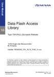
1
User’s Manual
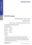
RL78 Family
Data Flash Library Type04
16
Japanese Release
ZIP file name : JP_R_FDL_RL78_T04_Vx.xx_x_E
16-Bit Single-Chip Microcontrollers
All information contained in these materials, including products and product specifications,
represents information on the product at the time of publication and is subject to change by
Renesas Electronics Corp. without notice. Please review the latest information published by
Renesas Electronics Corp. through various means, including the Renesas Electronics Corp.
website (http://www.renesas.com).
www.renesas.com
Rev.1.05
Dec 2014
Notice
1.
Descriptions of circuits, software and other related information in this document are provided only to illustrate the operation of
semiconductor products and application examples. You are fully responsible for the incorporation of these circuits, software,
and information in the design of your equipment. Renesas Electronics assumes no responsibility for any losses incurred by you
or third parties arising from the use of these circuits, software, or information.
2.
Renesas Electronics has used reasonable care in preparing the information included in this document, but Renesas Electronics
does not warrant that such information is error free. Renesas Electronics assumes no liability whatsoever for any damages
incurred by you resulting from errors in or omissions from the information included herein.
3.
Renesas Electronics does not assume any liability for infringement of patents, copyrights, or other intellectual property rights of
third parties by or arising from the use of Renesas Electronics products or technical information described in this document. No
license, express, implied or otherwise, is granted hereby under any patents, copyrights or other intellectual property rights of
Renesas Electronics or others.
4.
You should not alter, modify, copy, or otherwise misappropriate any Renesas Electronics product, whether in whole or in part.
Renesas Electronics assumes no responsibility for any losses incurred by you or third parties arising from such alteration,
modification, copy or otherwise misappropriation of Renesas Electronics product.
5.
Renesas Electronics products are classified according to the following two quality grades: “Standard” and “High Quality”. The
recommended applications for each Renesas Electronics product depends on the product’s quality grade, as indicated below.
“Standard”:
Computers; office equipment; communications equipment; test and measurement equipment; audio and visual
equipment; home electronic appliances; machine tools; personal electronic equipment; and industrial robots etc.
“High Quality”: Transportation equipment (automobiles, trains, ships, etc.); traffic control systems; anti-disaster systems; anticrime systems; and safety equipment etc.
Renesas Electronics products are neither intended nor authorized for use in products or systems that may pose a direct threat to
human life or bodily injury (artificial life support devices or systems, surgical implantations etc.), or may cause serious property
damages (nuclear reactor control systems, military equipment etc.). You must check the quality grade of each Renesas
Electronics product before using it in a particular application. You may not use any Renesas Electronics product for any
application for which it is not intended. Renesas Electronics shall not be in any way liable for any damages or losses incurred
by you or third parties arising from the use of any Renesas Electronics product for which the product is not intended by Renesas
Electronics.
6.
You should use the Renesas Electronics products described in this document within the range specified by Renesas Electronics,
especially with respect to the maximum rating, operating supply voltage range, movement power voltage range, heat radiation
characteristics, installation and other product characteristics. Renesas Electronics shall have no liability for malfunctions or
damages arising out of the use of Renesas Electronics products beyond such specified ranges.
7.
Although Renesas Electronics endeavors to improve the quality and reliability of its products, semiconductor products have
specific characteristics such as the occurrence of failure at a certain rate and malfunctions under certain use conditions. Further,
Renesas Electronics products are not subject to radiation resistance design. Please be sure to implement safety measures to
guard them against the possibility of physical injury, and injury or damage caused by fire in the event of the failure of a Renesas
Electronics product, such as safety design for hardware and software including but not limited to redundancy, fire control and
malfunction prevention, appropriate treatment for aging degradation or any other appropriate measures. Because the evaluation
of microcomputer software alone is very difficult, please evaluate the safety of the final products or systems manufactured by
you.
8.
Please contact a Renesas Electronics sales office for details as to environmental matters such as the environmental compatibility
of each Renesas Electronics product. Please use Renesas Electronics products in compliance with all applicable laws and
regulations that regulate the inclusion or use of controlled substances, including without limitation, the EU RoHS Directive.
Renesas Electronics assumes no liability for damages or losses occurring as a result of your noncompliance with applicable laws
and regulations.
9.
Renesas Electronics products and technology may not be used for or incorporated into any products or systems whose
manufacture, use, or sale is prohibited under any applicable domestic or foreign laws or regulations. You should not use
Renesas Electronics products or technology described in this document for any purpose relating to military applications or use
by the military, including but not limited to the development of weapons of mass destruction. When exporting the Renesas
Electronics products or technology described in this document, you should comply with the applicable export control laws and
regulations and follow the procedures required by such laws and regulations.
10. It is the responsibility of the buyer or distributor of Renesas Electronics products, who distributes, disposes of, or otherwise
places the product with a third party, to notify such third party in advance of the contents and conditions set forth in this
document, Renesas Electronics assumes no responsibility for any losses incurred by you or third parties as a result of
unauthorized use of Renesas Electronics products.
11. This document may not be reproduced or duplicated in any form, in whole or in part, without prior written consent of Renesas
Electronics.
12. Please contact a Renesas Electronics sales office if you have any questions regarding the information contained in this document
or Renesas Electronics products, or if you have any other inquiries.
(Note 1) “Renesas Electronics” as used in this document means Renesas Electronics Corporation and also includes its majorityowned subsidiaries.
(Note 2) “Renesas Electronics product(s)” means any product developed or manufactured by or for Renesas Electronics.
(2012.4)
General Precautions in the Handling of MPU/MCU Products
The following usage notes are applicable to all MPU/MCU products from Renesas. For detailed usage notes on the
products covered by this document, refer to the relevant sections of the document as well as any technical updates that
have been issued for the products.
1. Handling of Unused Pins
Handle unused pins in accordance with the directions given under Handling of Unused Pins in the
manual.
⎯ The input pins of CMOS products are generally in the high-impedance state. In operation with an
unused pin in the open-circuit state, extra electromagnetic noise is induced in the vicinity of LSI, an
associated shoot-through current flows internally, and malfunctions occur due to the false
recognition of the pin state as an input signal become possible. Unused pins should be handled as
described under Handling of Unused Pins in the manual.
2. Processing at Power-on
The state of the product is undefined at the moment when power is supplied.
⎯ The states of internal circuits in the LSI are indeterminate and the states of register settings and
pins are undefined at the moment when power is supplied.
In a finished product where the reset signal is applied to the external reset pin, the states of pins
are not guaranteed from the moment when power is supplied until the reset process is completed.
In a similar way, the states of pins in a product that is reset by an on-chip power-on reset function
are not guaranteed from the moment when power is supplied until the power reaches the level at
which resetting has been specified.
3. Prohibition of Access to Reserved Addresses
Access to reserved addresses is prohibited.
⎯ The reserved addresses are provided for the possible future expansion of functions. Do not access
these addresses; the correct operation of LSI is not guaranteed if they are accessed.
4. Clock Signals
After applying a reset, only release the reset line after the operating clock signal has become stable.
When switching the clock signal during program execution, wait until the target clock signal has
stabilized.
⎯ When the clock signal is generated with an external resonator (or from an external oscillator)
during a reset, ensure that the reset line is only released after full stabilization of the clock signal.
Moreover, when switching to a clock signal produced with an external resonator (or by an external
oscillator) while program execution is in progress, wait until the target clock signal is stable.
5. Differences between Products
Before changing from one product to another, i.e. to a product with a different part number, confirm
that the change will not lead to problems.
⎯ The characteristics of an MPU or MCU in the same group but having a different part number may
differ in terms of the internal memory capacity, layout pattern, and other factors, which can affect
the ranges of electrical characteristics, such as characteristic values, operating margins, immunity
to noise, and amount of radiated noise. When changing to a product with a different part number,
implement a system-evaluation test for the given product.
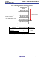
HOW TO USE THIS MANUAL
Readers
This manual is intended for user engineers who wish to understand the functions of the
RL78 microcontrollers Data Flash Library Type 04 and design and develop application
systems and programs for these devices.
Refer to the following list for the target MCUs.
Self-Programming Library (Japanese Release) and Supported MCUs (R20UT2861XJxxxx)
Purpose
This manual is intended to give users an understanding of the methods (described in the
Organization below) for using the Data Flash Library Type 04 to rewrite the data flash
memories.
The RL78 Data Flash Library Type 04 user’s manual is separated into the following parts:
Organization
Overview
Programming Environment
Data Flash Library Function
How to Read This Manual
It is assumed that the readers of this manual have general knowledge of electrical
engineering, logic circuits, and microcontrollers.
To gain a general understanding of functions:
Read this manual in the order of the CONTENTS.
To know details of the RL78 Microcontroller instructions:
Refer to CHAPTER 3 DATA FLASH LIBRARY FUNCTION.
The mark <R> shows major revised points.
Conventions
Data significance:
Higher digits on the left and lower digits on the right
Active low representations: (overscore over pin and signal name)
Note:
Footnote for item marked with Note in the text
Caution:
Information requiring particular attention
Remark:
Supplementary information
... or B
Numerical representations: Binary
...
Decimal
Hexadecimal
H
All trademarks and registered trademarks are the property of their respective owners.
EEPROM is a trademark of Renesas Electronics Corporation.
CONTENTS
CHAPTER 1 OVERVIEW .............................................................................................. 1
1. 1 Overview ....................................................................................................................................... 1
1. 2 Calling Data Flash Library Type 04 ............................................................................................... 3
CHAPTER 2 PROGRAMMING ENVIRONMENT .......................................................... 7
2. 1 Hardware Environment ................................................................................................................. 7
2. 1. 1 Initialization ...................................................................................................................... 9
2. 1. 2 Data flash control register (DFLCTL) .............................................................................. 9
2. 1. 3 Blocks ............................................................................................................................ 10
2. 1. 4 Processing time of Data Flash Library Type 04 ............................................................ 11
2. 2 Software Environment................................................................................................................. 18
2. 2. 1 Software resources of the R5F10266 product .............................................................. 20
2. 2. 2 Self-RAM ....................................................................................................................... 23
2. 2. 3 Register bank ................................................................................................................ 23
2. 2. 4 Stack and data buffer .................................................................................................... 23
2. 2. 5 Data flash library ........................................................................................................... 23
2. 2. 6 Program area ................................................................................................................ 24
2. 3 Cautions on Programming Environment ..................................................................................... 25
CHAPTER 3 DATA FLASH LIBRARY FUNCTION ...................................................... 27
3. 1 Type of Data Flash Library Functions ......................................................................................... 27
3. 2 Segments of Data Flash Library Functions ................................................................................. 27
3. 3 Commands ................................................................................................................................. 27
3. 4 BGO (Background Operation) .................................................................................................... 28
3. 5 List of Data Types, Return Values, and Return Types ................................................................ 30
3. 6 Description of Data Flash Library Functions ............................................................................... 31
APPENDIX A REVISION HISTORY ............................................................................ 41
A. 1 Major Revisions in This Edition .................................................................................................. 41
A. 2 Revision History of Preceding Editions ....................................................................................... 42
Index-1
RL78 Family
R01US0049EJ0105
Rev.1.05
Dec 22, 2014
Data Flash Library Type 04
CHAPTER 1 OVERVIEW
1. 1 Overview
The data flash library is a software library to perform operations to the data flash memory with the firmware
installed on the RL78 microcontroller.
The data flash library performs rewriting and reading of the data flash memory when called from the user
program.
Use this data flash library user's manual with the user's manual of the target RL78 microcontroller.
Terms The meanings of the terms used in this manual are described below.
• Data flash library
Library for data flash memory operations with the functions provided by the RL78 microcontroller.
It cannot perform operation to the code flash memory.
• Flash self-programming library
Library for code flash memory operation with the functions provided by the RL78 microcontroller.
Operation to the data flash memory cannot be done.
• EEPROM emulation library
Library that provides functions to store data to the built-in flash memory like an EEPROM.
• Block number
Number that shows a block of the flash memory.
It is the unit of erasure operation in the Data Flash Library
Type 04.
• Internal verification
To check if the signal level of the flash memory cell is appropriate after writing to the flash memory.
occurs in internal verification, the device is determined as failed.
If an error
However, if data erasure, data writing, and
internal verification are performed and completed normally after the internal verification error, the device is
determined as normal.
• FDL
Abbreviation of "Data Flash Library."
• Sequencer
The RL78 microcontroller has a dedicated circuit for controlling the flash memory.
In this document, this circuit
is called the "sequencer."
R01US0049EJ0105
Dec 22, 2014
Rev.1.05
Page 1 of 43
RL78 Family
CHAPTER 1
OVERVIEW
Data Flash Library Type 04
• BGO (background operation)
State in which rewriting of the flash memory can be done while operating the user program by letting the
sequencer to control the flash memory.
For the overview and details, refer to "2.1 Hardware Environment"
and "3.4 BGO (background operation)."
• Status check
When the sequencer is used, the processing to check the state of the sequencer (state of control for the flash
memory) with the program controlling the flash memory is required. In this document, the processing to check
the state of the sequencer is called "status checking."
R01US0049EJ0105
Dec 22, 2014
Rev.1.05
Page 2 of 43
RL78 Family
CHAPTER 1
OVERVIEW
Data Flash Library Type 04
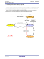
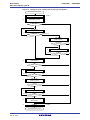
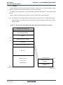
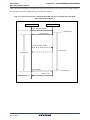
1. 2 Calling Data Flash Library Type 04
To perform rewriting of the data flash memory with the Data Flash Library Type 04, the initialization processing
for the Data Flash Library Type 04 and the functions corresponding to the functions used need to be executed
from the user program by using the C language or assembly language.
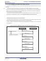
Figure 1-1 shows the state transition diagram of the Data Flash Library Type 04.
Figure 1-2 shows an
example of the code flash memory rewriting flow by using the Data Flash Library Type 04.
Figure 1-1.
State Transition Diagram of Data Flash Library Type 04
Reset or Power ON
uninitialized /
closed
PFDL_Open()
(DFLEN = 1)
PFDL_Close()
(DFLEN = 0)
Destroy RAM data
PFDL_Execute()
*Read command Only
Busy
opened
Return
PFDL_Execute()
PFDL_Handler()
Sequencer control
R01US0049EJ0105
Dec 22, 2014
Rev.1.05
Return
Sequencer busy
Page 3 of 43
RL78 Family
CHAPTER 1
OVERVIEW
Data Flash Library Type 04
[Overview of the state transition diagram]
To operate the data flash memory by using the Data Flash Library Type 04, the provided functions need to be
executed sequentially to perform processing. For details of functions, refer to section 3, Data Flash Library
Function.
(1) uninitialized/closed
State at Power ON and Reset.
To execute the flash self-programming library, EEPROM emulation library,
data flash library other than Type 04, STOP command, or HALT command, execute PFDL_Close from the
opened state to cause a transition to this state.
(2) opened
State in which the PFDL_Open() function has been executed from the uninitialized / closed state and the
data flash library can be executed.
In the period from the execution of PFDL_Close to the transition to the
uninitialized / closed state, the flash self-programming library, EEPROM emulation library, data flash library
other than Type 04, STOP command, or HALT command cannot be executed.
When the PFDL_Open function is executed, the data flash control register (DFLCTL) is set to the state
where accessing the data flash memory is permitted (DFLEN = 1), and when the PFDL_Close function is
executed, the DFLCTL is set to the access inhibit state (DFLEN = 0).
(3) busy
State in which the specified processing is being executed. The control does not return to the user
program until the processing is completed.
(4) sequencer busy
State in which the specified processing is being executed with the sequencer.
The PFDL_Execute
function specifies the details of control to the data flash memory, and the PFDL_Hander function performs
a status check.
The executed function returns to the user program without waiting for the completion of
sequencer operation.
R01US0049EJ0105
Dec 22, 2014
Rev.1.05
The code flash memory cannot be referred to while the sequencer is being used.
Page 4 of 43
RL78 Family
CHAPTER 1
OVERVIEW
Data Flash Library Type 04
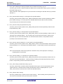
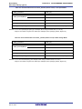
Figure 1-2
Example of Flow of Data Flash Library Type 04 Operation
Start data flash memory control
<1>
* DFLEN = 1
PFDL_Open
PFDL_Execute
<2>
(BLANKCHECK command)
Error
Status check
In control
<8>
PFDL_Handler
In control
Blank check error
Status check
Normal completion
PFDL_Execute
<3>
(ERASE command)
Status check
Error
In control
<8>
PFDL_Handler
In control
Status check
Error
Normal completion
PFDL_Execute
<4>
(WRITE command)
Error
Status check
In control
<8>
PFDL_Handler
In control
Error
Status check
Normal completion
PFDL_Execute
<5>
(IVERIFY command)
Error
Status check
In control
<8>
PFDL_Handler
In control
Error
Status check
Normal completion
PFDL_Execute
<6>
(READ command)
<7>
PFDL_Close
* DFLEN = 0
End data flash memory control
R01US0049EJ0105
Dec 22, 2014
Rev.1.05
Page 5 of 43
RL78 Family
CHAPTER 1
OVERVIEW
Data Flash Library Type 04
<1>
PFDL_Open: Initializing and starting the RAM used for the Data Flash Library Type 04
The PFDL_Open function is called to initialize the RAM used for the Data Flash Library Type 04 to enable the
Data Flash Library Type 04.
Set the data flash control register (DFLCTL) to the state where accessing the data flash memory is permitted
(DFLEN = 1).
<2>
PFDL_Execute: Blank checking 1 to 1024 bytes for the specified address
The PFDL_Execute function (with the PFDL_CMD_BLANKCHECK_BYTES command specified) is called to
perform blank checking of 1 to 1024 bytes for the specified address (confirm that the area is writable).
The processing cannot be executed across blocks.
<3>
PFDL_Execute: Erasing the specified block (1 KB)
The PFDL_Execute function (with the PFDL_CMD_ERASE_BLOCK command specified) is called to erase
the specified block (1 KB).
<4>
PFDL_Execute: Writing 1 to 1024-byte data to the specified address
The PFDL_Execute function (with the PFDL_CMD_WRITE_BYTES command specified) is called to write 1 to
1024 bytes to the specified address.
The processing cannot be executed across blocks. Writing can be
performed only to an area in the blank state or an area that has been erased. It is impossible to rewrite
(overwrite) an area that has been written.
<5>
PFDL_Execute: Internal verification of 1 to 1024 bytes for the specified address
The PFDL_Execute function (with the PFDL_CMD_IVERIFY_BYTES command specified) is called to perform
internal verification of 1 to 1024 bytes for the specified address.
The processing cannot be executed across
blocks.
Note: Internal verification checks if the signal level of the flash memory cell is appropriate. Checking by
comparing data is not performed.
<6>
PFDL_Execute: Reading 1 to 1024 bytes for the specified address
The PFDL_Execute function (with the PFDL_CMD_READ_BYTES command specified) is called to read 1 to
1024 bytes for the specified address.
All the processing of reading is executed within the PFDL_Execute
function. The processing cannot be executed across blocks.
<7>
PFDL_Close: Ending the Data Flash Library Type 04
The PFDL_Close function is called to end the Data Flash Library Type 04. Also set the data flash control
register (DFLCTL) to the state where accessing the data flash memory is inhibited (DFLEN = 0). The
PFDL_Close function is executed to end control of the data flash memory.
<8>
PFDL_Handler: Status checking
The PFDL_Handler function is called to perform status checking.
Status checking must be performed until
the control to the data flash memory by the sequencer is finished.
R01US0049EJ0105
Dec 22, 2014
Rev.1.05
Page 6 of 43
RL78 Family
CHAPTER 2
PROGRAMMING ENVIRONMENT
Data Flash Library Type 04
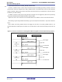
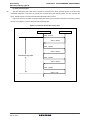
CHAPTER 2 PROGRAMMING ENVIRONMENT
This chapter describes the hardware environment and software environment required to rewrite the data flash
memory using the Data Flash Library Type 04.
2. 1 Hardware Environment
The Data Flash Library Type 04 for the RL78 microcontroller uses the sequencer to execute rewrite control of
the data flash memory.
Because the sequencer controls the data flash memory, the user program can be
operated during data flash memory control.
This is called BGO (background operation).
During rewriting of the data flash memory, the data flash memory cannot be referred to. However, the code
flash memory can be referred to, so interrupt processing, user program, and Data Flash Library Type 04 can be
allocated in the ROM for operation as usual.
Note
Figure 2-1 shows the state during a rewrite of the data flash memory.
Figure 2-2 shows an example of
execution of the flash library functions to perform rewriting of the data flash memory.
Figure 2-1
State during Rewrite of Data Flash Memory
Internal RAM
Data flash memory
The user program can operate as
usual with the BGO (background
operation) during data flash memory
control.
×
Reading cannot be executed
during data flash memory control.
Code flash memory
Interrupts can be used as usual.
Note: Interrupts are inhibited for the R5F10266 product.
R01US0049EJ0105
Dec 22, 2014
Rev.1.05
Page 7 of 43
RL78 Family
CHAPTER 2
PROGRAMMING ENVIRONMENT
Data Flash Library Type 04
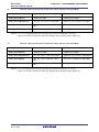
Figure 2-2
Example of Rewrite Control of Data Flash Memory
•After an execution request of the desired processing is made to the sequencer of the RL78 microcontroller,
the control is immediately returned to the user program.
For the result of the control of the data flash
memory, the status check function (PFDL_Handler function) must be called from the user program to check
the control state of the data flash memory.
User program
Library
Sequencer
Call
Execute
On going
Ret (BUSY)
Call
Execute
On going
Data flash memory
cannot be referred to
during this period
Ret (BUSY)
Call
Execute
Finish
Ret (OK)
R01US0049EJ0105
Dec 22, 2014
Rev.1.05
Page 8 of 43
RL78 Family
CHAPTER 2
PROGRAMMING ENVIRONMENT
Data Flash Library Type 04
2. 1. 1 Initialization
When rewriting the data flash memory by using the Data Flash Library Type 04, make the following settings.
(1) Starting high-speed on-chip oscillator
During use of the Data Flash Library Type 04, keep the high-speed on-chip oscillator running. When the
oscillator is stopped, start it before using the Data Flash Library Type 04.
(2) Setting CPU operating frequency
Note1
In order to calculate the timing in the Data Flash Library Type 04, set the CPU operating frequency at
initialization. For the method for setting the frequency, see the description of the PFDL_Open() function.
(3) Setting flash memory programming mode
Note2
In order to set the flash memory programming mode for writing, either of the flash memory programming
modes shown below should be specified when initializing the Data Flash Library Type 04.
See the
description of the PFDL_Open function for the settings of the flash memory programming modes.
- Full speed mode
- Wide voltage mode
Notes 1. The CPU operating frequency is used as a parameter for the calculation of internal timing used in the
Data Flash Library Type 04. This setting does not affect the CPU operating frequency.
This is not the
operating frequency for the high-speed on-chip oscillator.
2. For details of the flash memory programming mode, see the target RL78 microcontroller user’s
manual.
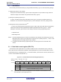
2. 1. 2 Data flash control register (DFLCTL)
The data flash control register (DFLCTL) enables or disables access to the data flash memory. When the
PFDL_Open function is executed, the data flash control register (DFLCTL) is set to the state where access to
the data flash memory is enabled (DFLEN = 1), and when the PFDL_Close function is executed, the DFLCTL is
set to the access disabled state (DFLEN = 0).
Figure 2-3
Format of Data Flash Control Register (DFLCTL)
Address : F0090H Initial value : 00H
R/W
Abbreviation
7
6
5
4
3
2
1
0
DFLCTL
0
0
0
0
0
0
0
DFLEN
Note:
DFLEN
Controlling access to the data flash memory
0
Access to the data flash memory is disabled
1
Access to the data flash memory is enabled
Refer to the user’s manual of the target RL78 microcontroller for more information on the settings
of the data flash control register (DFLCTL).
R01US0049EJ0105
Dec 22, 2014
Rev.1.05
Page 9 of 43
RL78 Family
CHAPTER 2
PROGRAMMING ENVIRONMENT
Data Flash Library Type 04
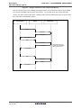
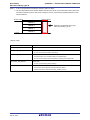
2. 1. 3 Blocks
The flash memory of the RL78 microcontroller is divided into 1-Kbyte blocks. In the data flash library, erasure
processing is performed for the data flash memory in the units of the blocks.
For reading, writing, blank checking, or internal verification, specify the start address
Note
and execution size for
execution.
Figure 2-3 shows an example of block positions and block numbers of the data flash memory.
Note
The address value used when reading and writing data in the flash memory. is a relative address that
starts from block 0 of the data flash memory (block 0 is assumed as address 0). Note that this is not an
absolute address.
Figure 2-3
Blocks of Data Flash Memory (RL78/G12: When Data Flash Memory Is 2 Kbytes)
Special function register SFR
General registers
Internal high-speed RAM
Mirror
F17FFH
Data flash memory (2 Kbytes)
F1000H
Not used
Special function register 2nd SFR
Not used
1 Kbytes/2 blocks
07FFH
Code flash memory
User program
+
Data flash library
Data flash memory
Block 1
0400H
Data flash memory
Block 0
00000H
0000H
Absolute address
R01US0049EJ0105
Dec 22, 2014
Relative address
Rev.1.05
Page 10 of 43
RL78 Family
CHAPTER 2
PROGRAMMING ENVIRONMENT
Data Flash Library Type 04
2. 1. 4 Processing time of Data Flash Library Type 04
This section describes the time required to process Data Flash Library Type 04 functions (except for the Read
command).
<R>
The number of clock cycles required to execute flash functions differs depending on whether the flash
functions are allocated to the internal ROM area (flash memory) or they are allocated to the internal RAM area.
When the functions are executed in the RAM, the processing time may increase to a maximum of double the
time needed when they are executed in the ROM.
This section shows the processing time when the data flash library functions are executed in the ROM.
For
each segment of data flash library functions, see 3.2 Segments of Data Flash Library Functions.
(1) Data Flash Library Type 04 function processing time
The flash function processing time is the time required from when a user-created program calls a flash
function until the processing ends and control returns to the user-created program.
Figure 2-5 shows an overview of the flash function processing time, and Tables 2-1 and 2-2 show the
processing time.
Figure 2-5. Overview of Data Flash Library Type 04 Function Processing Time
User Program
FDL
PFDL_Execute
Status = BUSY
Function Processing Time
PFDL_Handler
Status = BUSY
PFDL_Handler
Status = BUSY
PFDL_Handler
Status = OK
R01US0049EJ0105
Dec 22, 2014
Rev.1.05
Page 11 of 43
RL78 Family
CHAPTER 2
PROGRAMMING ENVIRONMENT
Data Flash Library Type 04
Table 2-1. Function Processing Time in Full Speed Mode
PFDL_Functions
Max. (μs)
PFDL_Open
862 / fCLK
PFDL_Execute(Erase)
536 / fCLK
PFDL_Execute(BlankCheck)
484 / fCLK
PFDL_Execute(Write)
549 / fCLK
PFDL_Execute(IVerify)
502 / fCLK
PFDL_Execute(Read)
53 / fCLK + 17 / fCLK × Bytes
PFDL_Handler
251 / fCLK + 14
PFDL_Close
823 / fCLK + 443
PFDL_GetVersionString
10 / fCLK
Remarks 1. fCLK: CPU operating frequency (For example, when using a 20 MHz clock, f CLK is 20.)
2. Bytes: The number of bytes to be written (For example, when specifying 8 bytes, Bytes is 8.)
<R>
Table 2-2. Function Processing Time in Wide Voltage Mode
PFDL_Functions
Max. (μs)
PFDL_Open
862 / fCLK
PFDL_Execute(Erase)
536 / fCLK
PFDL_Execute(BlankCheck)
484 / fCLK
PFDL_Execute(Write)
549 / fCLK
PFDL_Execute(IVerify)
502 / fCLK
PFDL_Execute(Read)
53 / fCLK + 17 / fCLK × Bytes
PFDL_Handler
251 / fCLK + 14
PFDL_Close
779 / fCLK + 968
PFDL_GetVersionString
10 / fCLK
Remarks 1. fCLK: CPU operating frequency (For example, when using a 20 MHz clock, f CLK is 20.)
2. Bytes: The number of bytes to be written (For example, when specifying 8 bytes, Bytes is 8.)
R01US0049EJ0105
Dec 22, 2014
Rev.1.05
Page 12 of 43
RL78 Family
CHAPTER 2
PROGRAMMING ENVIRONMENT
Data Flash Library Type 04
<R>
(2) Recommended interval of PFDL_Handler (status check)
The PFDL_Handler function is used to check the status except for the reading processing. However, the end of
each process cannot be confirmed if the PFDL_Handler function is executed before control by the sequencer
finishes. Therefore, spacing each process executed by each flash function by a specific time is useful to enhance
the efficiency of status checking.
In addition, because a write process using the Write command must be triggered by status check processing
every byte, the status must be checked each time 1 byte is written.
Figures 2-6 and 2-7 show overviews of recommended interval, and Tables 2-3 and 2-4 show the interval time.
When writing 3 bytes using the Data Flash Library Type 04, the sequencer writes data in 1-byte units. Therefore,
when 1
byte is written, the PFDL_Handler function must trigger the next write. If the PFDL_Handler function is not
executed while there are still bytes to be written, the next write does not start, and thus the write process does not
end.
Figure 2-6. Overview of Interval for Checking Status When Using Write Command (When Writing 3 Bytes)
User Program
FDL
PFDL_Execute
Status = BUSY
Write trigger
1-byte write
Call Interval
PFDL_Handler
Status = BUSY
1st write ends
Write trigger
1-byte write
Call Interval
PFDL_Handler
Status = BUSY
2nd write ends
Write trigger
1-byte write
Call Interval
PFDL_Handler
3rd write ends
Status = OK
R01US0049EJ0105
Dec 22, 2014
Rev.1.05
Page 13 of 43
RL78 Family
CHAPTER 2
PROGRAMMING ENVIRONMENT
Data Flash Library Type 04
When a process is executed by a command other than Write, the sequencer is in the busy state until all processes
end. A trigger by the PFDL_Handler function is therefore not required.
Figure 2-7. Overview of Interval for Checking Status When Using a Command Other Than Write
(When Erasing Flash Memory)
User Program
FDL
PFDL_Execute (Erase)
Erase trigger
Status = BUSY
No call for PFDL_Handler
1-block erase
Call Interval
PFDL_Handler
Erase ends
Status = OK
R01US0049EJ0105
Dec 22, 2014
Rev.1.05
Page 14 of 43
RL78 Family
CHAPTER 2
PROGRAMMING ENVIRONMENT
Data Flash Library Type 04
Table 2-3. Recommended Interval of PFDL_Handler (Status Check) in Full Speed Mode
Max. (μs)
PFDL_Functions
When block is blank
5860 / fCLK + 335
When block is not blank
12734 / fCLK + 6946
PFDL_Execute(Erase)
PFDL_Execute(BlankCheck)
33 / fCLK + 18 + (6 / fCLK + 0.31) × Bytes
PFDL_Execute(Write)
61 / fCLK + 47
PFDL_Execute(IVerify)
13 / fCLK + 17 + (28 / fCLK + 4) × Bytes
Remarks 1. fCLK: CPU operating frequency (For example, when using a 20 MHz clock, f CLK is 20.)
2. Bytes: The number of bytes to be written (For example, when specifying 8 bytes, Bytes is 8.)
Table 2-4. Recommended Interval of PFDL_Handler (Status Check) in Wide Voltage Mode
Max. (μs)
PFDL_Functions
When block is blank
5065 / fCLK + 1167
When block is not blank
11144 / fCLK + 8620
PFDL_Execute(Erase)
PFDL_Execute(BlankCheck)
30 / fCLK + 57 + (5 / fCLK + 1.084) × Bytes
PFDL_Execute(Write)
57 / fCLK + 99
PFDL_Execute(IVerify)
14 / fCLK + 44 + (17 / fCLK + 29) × Bytes
Remarks 1. fCLK: CPU clock frequency (For example, when using a 20 MHz clock, f CLK is 20.)
2. Bytes: The number of bytes to be written (For example, when specifying 8 bytes, Bytes is 8.)
R01US0049EJ0105
Dec 22, 2014
Rev.1.05
Page 15 of 43
RL78 Family
CHAPTER 2
PROGRAMMING ENVIRONMENT
Data Flash Library Type 04
(3) Total processing time
<R>
The total processing time when each command is executed in the PFDL_Execute function is the time until
successful termination. This does not include the overhead time (call interval) before the user executes the
PFDL_Handler function or the time until abnormal termination due to errors.
Figure 2-8 shows an overview of total processing time when each command is executed in the PFDL_Execute
function, and Tables 2-5 and 2-6 show the total processing time.
Figure 2-8. Overview of Total Processing Time
User Program
FDL
PFDL_Execute
Status = BUSY
PFDL_Handler
Status = BUSY
Total Processing Time
PFDL_Handler
Status = BUSY
PFDL_Handler
Status = OK
R01US0049EJ0105
Dec 22, 2014
Rev.1.05
Page 16 of 43
RL78 Family
CHAPTER 2
PROGRAMMING ENVIRONMENT
Data Flash Library Type 04
<R>
Table 2-5. Total Processing Time of Data Flash Library Type 04 in Full Speed Mode
PFDL_Functions
Typical (μs)
Max. (μs)
PFDL_Execute(Erase)
11250 / fCLK + 5800
281561 / fCLK + 264790
PFDL_Execute(BlankCheck)
906 / fCLK + 30 + (5 / fCLK +0.26) × Bytes
1088 / fCLK + 36 + (6 / fCLK + 0.31) × Bytes
487 / fCLK + 11.67 + (212 / fCLK + 39.17) ×
Bytes
PFDL_Execute(Write)
621 / fCLK + 25 + (23 / fCLK + 3.33) × Bytes
PFDL_Execute(IVerify)
585 / fCLK + 14 + (714 / fCLK + 430) × Bytes
746 / fCLK + 30 + (28 / fCLK + 4) × Bytes
Remarks 1. fCLK: CPU operating frequency (For example, when using a 20 MHz clock, fCLK is 20.)
2. Bytes: The number of bytes to be written (For example, when specifying 8 bytes, Bytes is 8.)
<R>
Table 2-6. Total Processing Time of Data Flash Library Type 04 in Full Speed Mode
PFDL_Functions
Typical (μs)
Max. (μs)
PFDL_Execute(Erase)
9925 / fCLK + 7194.17
249000 / fCLK + 299307
PFDL_Execute(BlankCheck)
903 / fCLK + 62.5 + (4 / fCLK +0.9) × Bytes
1084 / fCLK + 75 + (5 / fCLK + 1.084) × Bytes
PFDL_Execute(Write)
487 / fCLK + 11.67 + (208 / fCLK + 82.5) ×
Bytes
585 / fCLK + 14 + (669 / fCLK + 954) × Bytes
PFDL_Execute(IVerify)
622 / fCLK + 48.33 + (14 / fCLK + 24.17) ×
Bytes
747 / fCLK + 58 + (17 / fCLK + 29) × Bytes
Remarks 1. fCLK: CPU operating frequency (For example, when using a 20 MHz clock, f CLK is 20.)
2. Bytes: The number of bytes to be written (For example, when specifying 8 bytes, Bytes is 8.)
R01US0049EJ0105
Dec 22, 2014
Rev.1.05
Page 17 of 43
RL78 Family
CHAPTER 2
PROGRAMMING ENVIRONMENT
Data Flash Library Type 04
2. 2 Software Environment
Because the Data Flash Library Type 04 for the RL78 Family program needs to be allocated to the user area,
the size of the program code will be consumed in the user program area.
To run the data flash library, the CPU, stack, and data buffer are used.
Table 2-7 lists the software resources required
Note1, 2
, and Figures 2-9 and 2-10 show examples of arrangement
in RAM.
<R>
Table 2-7. Software Resources Used by Data Flash Library Type 04
Item
Size(Byte)
Note3
Self-RAM
Note3
0 to 136
Restrictions on Allocation and Usage
Note1,2
The self-RAM area used by RL78 Family Data Flash Library Type 04 Ver. 1.05 differs
depending on the device. For details, refer to "RL78 Family Self RAM list of Flash Self
Programming Library(R20UT2944)".
Note4
Stack
Data Buffer
Function
arguments
Note5
Library size
46 max.
1 to 1024
0 to 8
ROM: 177 max.
Can be allocated to a RAM area other than the self-RAM and the area from
Note2
FFE20H to FFEFFH
.
Can be allocated to a program area other than the self-RAM and the area from FFE20H to
FFEFFH.
<R> Notes: 1. For devices not shown in the RL78 Family Self RAM list of Flash Self Programming Library(R20UT2944),
contact your Renesas sales agency.
2. This table is not applicable to the R5F10266 product. Refer to 2.2.1 Software resources of the R5F10266
product.
3. An area used as the working area by the Data Flash Library Type 04 is called self-RAM in this manual and
the Release Note. The self-RAM requires no user setting because it is an area that is not mapped and
automatically used at execution of the data flash library (previous data is discarded). When the data flash
library is not used, the self-RAM can be used as a normal RAM space.
4. This is the sum of the amount of stack (maximum of 4 bytes) necessary for calling a function and 42 bytes
of stack used by the library.
5. The data buffer is a RAM area necessary for inputting data for reading and writing. The necessary size
changes according to the unit of reading and writing. When reading and writing of 1 byte is performed, the
required data buffer size is 1 byte.
R01US0049EJ0105
Dec 22, 2014
Rev.1.05
Page 18 of 43
RL78 Family
CHAPTER 2
PROGRAMMING ENVIRONMENT
Data Flash Library Type 04
Figure 2-9 Example 1 of Arrangement in RAM Including Self-RAM
(RL78/G13: Product with 4-Kbyte RAM and 64-Kbyte ROM)
Special function register (SFR)
FFEFFH
General-purpose registers 32 bytes
FFE20H
FFE1FH
SADDR area
Area where RAM (stack, data buffer, etc.)
used by the data flash library cannot be
allocated
No allocation restriction
RAM
4 Kbytes
FF300H
FF2FFH
Area whose usage is prohibited
(Self-RAM)
Area damaged when the data flash
library is used
FEF00H
FEEFFH
Mirror
Figure 2-10
Example 2 of Arrangement in RAM without Self-RAM
(RL78/G13: Product with 2-Kbyte RAM and 32-Kbyte ROM)
Special function register (SFR)
FFEFFH
General-purpose registers 32 bytes
FFE20H
FFE1FH
RAM
2 Kbytes
SADDR area
Area where RAM (stack, data buffer, etc.)
used by the data flash library cannot be
allocated
No allocation restriction
FF700H
FF6FFH
Mirror
R01US0049EJ0105
Dec 22, 2014
Rev.1.05
Page 19 of 43
RL78 Family
CHAPTER 2
PROGRAMMING ENVIRONMENT
Data Flash Library Type 04
2. 2. 1 Software resources of the R5F10266 product
The R5F10266 product has usage inhibited areas and restrictions on stack allocation. Therefore, the settings of
software resources differ from other products. Using an interrupt is also prohibited.
Table 2-8 shows a list of software resources necessary for the R5F10266 product; figure 2-11, an example of
RAM area; and figures 2-12 and 2-13, examples of a stack allocation for each language in use.
Table 2-8 Data Flash Library Type 04 Software Resources of the R5F10266 Product
Item
Size(Byte)
Note3
Self-RAM
0
Stack
46 max.
Data Buffer
Note3
Restrictions on Allocation and Usage
Note2, 3
There is no self-RAM.
Note1
Allocated in the RAM area of FFEA2H-FFEDFH Note2.
1 to 24
Can be allocated to a RAM area other than the area from FFE20H to FFEFFH.
Function arguments
8
Library size
ROM: 177 max.
Allocate in the code flash memory area.
Notes: 1. This is the sum of the amount of stack (maximum of 4 bytes) necessary for calling a function and 42 bytes
of stack used by the library.
2. Specify so that the stack used by the library is sure to be within this area.
3. The data buffer is a RAM area necessary for inputting data for reading and writing. The necessary size
changes according to the unit of reading and writing. When reading and writing of 1 byte is performed, the
required data buffer size is 1 byte.
Figure 2-11 Example of RAM Area When Data Flash Library is Used in the R5F10266 Product
Special function register (SFR)
FFEFFH
FFEE0H
General-purpose registers 32 bytes
Area where RAM (stack, data buffer, etc.)
used by the data flash library cannot be
allocated
Stack allocation area
(62 bytes)
Area where stack can be allocated when
the data flash library is used in the
R5F10266
SADDR area
(130 bytes)
Area where RAM (stack, data buffer, etc.)
used by the data flash library cannot be
allocated
No allocation restriction (32 bytes)
Area where RAM, except for the stack to
be used by the data flash library, can be
allocated
FFEDFH
FFEA2H
FFEA1H
RAM
256 bytes
FFE20H
FFE1FH
FFE00H
FFEFFH
Unusable
R01US0049EJ0105
Dec 22, 2014
Rev.1.05
Page 20 of 43
RL78 Family
CHAPTER 2
PROGRAMMING ENVIRONMENT
Data Flash Library Type 04
Figure 2-12 Example 1 of Stack Allocation
(for the R5F10266 product/ in the case of assembly language)
Special function register (SFR)
FFEFFH
General-purpose registers 32 bytes
FFEE0H
FFEDFH
The remaining user stack when the library
function is executed (16 bytes Note)
<R>
Area where the stack can be allocated
when the data flash library is used by the
R5F10266
Used by the stack of the library (46 bytes)
RAM
256 bytes
FFEA2H
FFEA1H
SADDR Area
(130 bytes)
FFE20H
FFE1FH
・
・
・
No allocation restriction (32 bytes)
Data buffer (1 to 24 bytes)
FFE00H
Allocate the argument sof the library
functions (8 bytes)
FFEFFH
Unusable
Note: When the on-chip debugging function is used, the stack space to be used by the on-chip debugging
function (4 bytes) is required, so this stack must be allocated in this area. When this stack is allocated, the
remaining space that can be used as the user stack while the Data Flash Library Type 04 is in use
becomes the remaining 12 bytes.
R01US0049EJ0105
Dec 22, 2014
Rev.1.05
Page 21 of 43
RL78 Family
CHAPTER 2
PROGRAMMING ENVIRONMENT
Data Flash Library Type 04
Figure 2-13 Example 2 of Stack Allocation
(for the R5F10266 product/ in the case of CubeSuite+: C language)
Special function register (SFR)
FFEFFH
General-purpose registers 32 bytes
FFEE0H
FFEDFH
FFED8H
Area used by the argument of a compiler or
run-time library (8 bytes)
FFED7H
The remaining user stack when the library
function is executed (8 bytes Note)
Used by the stack of the library (46 bytes)
Area where the stack can be allocated
when the data flash library is used by the
R5F10266 (in the case of C language)
RAM
256 bytes
FFEA2H
FFEA1H
SADDR Area
(130 bytes)
FFE20H
FFE1FH
・
・
・
No allocation restriction (32 bytes)
Data buffer (1 to 24 bytes)
FFE00H
Allocate the arguments of the library
functions (8 bytes)
FFEFFH
Unusable
Note: When using C language, the stack space (4 bytes) used when the main function is executed from the
start-up routine is required. When the on-chip debugging function is used, the stack space (4 bytes) used
by the on-chip debugging function is required. Thus, these stacks must be placed in this area. When both
of these stacks are used, the remaining space that can be used as the user stack while using Data Flash
Library Type 04 is 0 bytes.
R01US0049EJ0105
Dec 22, 2014
Rev.1.05
Page 22 of 43
RL78 Family
CHAPTER 2
PROGRAMMING ENVIRONMENT
Data Flash Library Type 04
<R>
2. 2. 2 Self-RAM
The Data Flash Library Type 04 may use a RAM area as the working area.
This area is called the
"self-RAM." The data used in the self-RAM is defined within the library, so no user definition of data is required.
When a data flash library function is called, the data in the self-RAM area is rewritten.
The self-RAM area used for data flash programming varies depending on the microcontroller, and the user
RAM may be used in some devices.
In such a device, the user needs to allocate the self-RAM area to the user RAM; be sure to allocate the
self-RAM area at linkage (the area can be specified in the link directive file).
2. 2. 3 Register bank
The Data Flash Library Type 04 uses the general registers, ES/CS register, SP, and PSW of the register bank
selected by the user.
2. 2. 4 Stack and data buffer
The Data Flash Library Type 04 uses the sequencer to write to the data flash memory, but it uses the CPU for
pre-setting and control.
Therefore, to use the Data Flash Library Type 04, the stack specified by the user
program is also required.
Remark
To allocate the stack and data buffer to the user-specified addresses, the link directive is used.
• Stack
In addition to the stack used by the user program, the stack space required for flash functions must be
reserved in advance, and they must be allocated so that the RAM used by the user will not be destroyed in
stack processing during Data Flash Library Type 04 operation.
The available range for stack specification
is the internal RAM excluding the self-RAM and addresses FFE20H to FFEFFH.
• Data buffer
The uses of the data buffer are as follows.
- Area in which data to be written is located during writing
- Area in which data to be obtained is located during reading
The available range for the start address of the data buffer is the internal RAM excluding the self-RAM and
RAM addresses FFE20H to FFEFFH, as in the stack.
2. 2. 5 Data flash library
Not all the data flash library functions are linked. Only the data flash library functions to be used are linked
Note
.
• Memory allocation of the Data Flash Library Type 04
Segments are assigned to the functions and variables used in the Data Flash Library Type 04.
Areas
used in the Data Flash Library Type 04 can be specified to the specific locations.
Note
For the assembly language, linking can be done only for the data flash library functions to be used by
deleting unnecessary functions from the include file.
R01US0049EJ0105
Dec 22, 2014
Rev.1.05
Page 23 of 43
RL78 Family
CHAPTER 2
PROGRAMMING ENVIRONMENT
Data Flash Library Type 04
2. 2. 6 Program area
This is the area in which the Data Flash Library Type 04 and the user program using the Data Flash Library
Type 04 are allocated.
In the Data Flash Library Type 04 for the RL78 microcontroller, the user program can be operated during
rewriting of the data flash memory because the data flash memory is rewritten by using the sequencer
(background operation).
R01US0049EJ0105
Dec 22, 2014
Rev.1.05
Page 24 of 43
RL78 Family
CHAPTER 2
PROGRAMMING ENVIRONMENT
Data Flash Library Type 04
2. 3 Cautions on Programming Environment
(1) Do not execute the flash self-programming library, EEPROM emulation library, or data flash library other than
Type 04 during the execution of the Data Flash Library Type 04. When using the flash self-programming library,
EEPROM emulation library, or data flash library other than Type 04, be sure to execute PFDL_Close to close the
data flash library.
(2) Do not execute the STOP or HALT instruction during the execution of the Data Flash Library Type 04.
If the
STOP or HALT instruction needs to be executed, be sure to execute the PFDL_Close function to close the data
flash library.
(3) The watchdog timer does not stop during the execution of the Data Flash Library Type 04.
(4) The data flash memory cannot be read during data flash memory operation by the Data Flash Library Type 04.
(5) Do not allocate the arguments (data buffer) or stack used in the data flash library function to an address over
0xFFE20 (0xFE20).
(6) When using the data transfer controller (DTC) during the execution of the Data Flash Library Type 04, do not
allocate the RAM area used by the DTC to the self-RAM or an address over 0xFFE20 (0xFE20).
(7) Do not use the RAM area (including self-RAM) used by the Data Flash Library Type 04 until data flash library is
completed.
(8) Do not execute a data flash library function within interrupt processing because the Data Flash Library Type 04
does not support multiple executions of data flash library functions.
(9) When executing the Data Flash Library Type 04 on the operating system, do not execute data flash library
functions from multiple tasks because the Data Flash Library Type 04 does not support multiple executions of
data flash library functions.
(10) Before starting the Data Flash Library Type 04, the high-speed on-chip oscillator needs to be started.
R01US0049EJ0105
Dec 22, 2014
Rev.1.05
Page 25 of 43
RL78 Family
CHAPTER 2
PROGRAMMING ENVIRONMENT
Data Flash Library Type 04
(11) Note the following regarding the operating frequency of the CPU and the operating frequency value set with the
initialization function (PFDL_Open).
- When a frequency below 4 MHz
Note1
is used as the operating frequency of the CPU, 1 MHz, 2 MHz, or 3 MHz
can be used (a frequency such as 1.5 MHz that is not an integer value cannot be used). Also, set an integer
value such as 1, 2, or 3 as the operating frequency value set with the initialization function.
- When 4 MHz
Note1
or a higher frequency is used as the operating frequency of the CPU, a frequency with
decimal places can be used.
However, set a rounded up integer value as the operating frequency with the
initialization function (PFDL_Open).
(Example: For 4.5 MHz, set "5" with the initialization function.)
- This operating frequency is not the frequency of the high-speed on-chip oscillator.
(12) The data flash control register (DFLCTL) should not be operated during the execution of the Data Flash Library
Type 04. In addition, when the Data Flash Library Type 04 is ended, the DFLCTL is set to access inhibit state by
the PFDL_Close function.
If accessing the data flash memory is required even after the Data Flash Library Type 04 is ended, confirm the
completion of the PFDL_Close function, set the DFLCTL to the access permit state, and perform the setup
process
Note2
.
(13) Initialize the arguments (RAM) that are used by the data flash library function. When they are not initialized, a
RAM parity error is detected and the RL78 microcontroller might be reset.
For a RAM parity error, refer to the user’s manual of the target RL78 microcontroller.
(14) Writing to the data flash memory can be performed only to an area in the blank state or the area that has been
erased. It is impossible to rewrite (overwrite) to an area that has been written unless it has been erased. When
rewriting is performed without erasing data, the data flash memory might be damaged.
(15) The Data Flash Library Type 04 does not perform error checking of the parameters set in the arguments of data
flash library functions.
Therefore, make sure to set a correct value to the parameter after checking the
specifications of the target RL78 microcontroller.
If parameter checking is required to set a correct value,
perform it in the user program.
(16) Interrupts are inhibited for the R5F10266 product while the Data Flash Library Type 04 is in use.
Notes 1. For the range of the operating frequency of the CPU, see the target RL78 microcontroller user's manual.
2. For the method of the setup, see the target RL78 microcontroller user's manual.
R01US0049EJ0105
Dec 22, 2014
Rev.1.05
Page 26 of 43
RL78 Family
CHAPTER 3
DATA FLASH LIBRARY FUNCTION
Data Flash Library Type 04
CHAPTER 3 DATA FLASH LIBRARY FUNCTION
This chapter describes the details of the data flash library functions.
3. 1 Type of Data Flash Library Functions
The Data Flash Library Type 04 consists of the following flash functions.
Table 3-1
List of Data Flash Library Functions
Function Name
Description
PFDL_Open
Initialization and starting of the RAM used for the Data Flash Library Type 04
PFDL_Close
Ending of the Data Flash Library Type 04
PFDL_Execute
Execution of control of the data flash memory
PFDL_Handler
Checking of the control state of the data flash memory and setting of continuous
execution (status check processing)
PFDL_GetVersionString
Acquisition of the version information of the Data Flash Library Type 04
3. 2 Segments of Data Flash Library Functions
The data flash library functions consist of the following segment.
•PFDL_COD:
Segment of the data flash library function.
This can be allocated to the ROM or RAM.
3. 3 Commands
The details of operation of the Data Flash Library Type 04 for the data flash memory can be specified with a
command in the argument of the PFDL_Execute function. The commands specified in the PFDL_Execute
function are shown below.
For details on the execution method, refer to the section on the PFDL_Execute
function.
Table 3-2.
List of Commands Specified in PFDL_Execute Function
Definition
Value
Command Name
PFDL_CMD_READ_BYTES
0x00
Read command
PFDL_CMD_BLANKCHECK_BYTES
0x08
Blank check command
PFDL_CMD_ERASE_BLOCK
0x03
Erasure command
PFDL_CMD_WRITE_BYTES
0x04
Write command
PFDL_CMD_IVERIFY_BYTES
0x06
Internal verification command
R01US0049EJ0105
Dec 22, 2014
Rev.1.05
Page 27 of 43
RL78 Family
CHAPTER 3
DATA FLASH LIBRARY FUNCTION
Data Flash Library Type 04
3. 4 BGO (Background Operation)
The data flash library functions can be divided into functions that do not use the sequencer and functions that
Note
use the sequencer
Note
. For the functions that use the sequencer
, BGO (background operation) can be
performed.
The following shows examples of operation of the Data Flash Library Type 04 during BGO and the presence of
sequencer control for each function.
Note
Not during the execution of the PFDL_CMD_READ_BYTES command.
Figure 3-1.
BGO Operation Example 1 (Write: Writing 3 Bytes)
User
Library
PFDL_Execute
function executed
Sequencer in operation
(Writing 1 byte)
PFDL_Execute function closed
(Return value: PFDL_BUSY)
PFDL_Handler function executed
PFDL_Handler function closed
(Return value: PFDL_BUSY)
PFDL_Handler function executed
Writing of 1 byte completed
Writing trigger
Sequencer in operation
(Writing 1 byte)
PFDL_Handler function closed
(Return value: PFDL_BUSY)
For writing, trigger processing
with the PFDL_Handler is
required for every byte.
Writing of 2 bytes completed
PFDL_Handler function executed
* Executing PFDL_Handler
before the sequencer
completes writing does not
result in trigger processing.
PFDL_Handler function closed
(Return value: PFDL_BUSY)
Writing trigger
Sequencer in operation
(Writing 1 byte)
PFDL_Handler function executed
Writing of all 3 bytes
completed
PFDL_Handler function closed
(Return value: PFDL_OK)
End of processing
R01US0049EJ0105
Dec 22, 2014
Rev.1.05
Page 28 of 43
RL78 Family
CHAPTER 3
DATA FLASH LIBRARY FUNCTION
Data Flash Library Type 04
Figure 3-2.
BGO Operation Example 2 (Erase, Iverify, BlankCheck)
User
Library
PFDL_Execute function
executed
PFDL_Execute function closed
(Return value: PFDL_BUSY)
PFDL_Handler function executed
Sequencer in operation
The control returns immediately, so other
processing can be executed. The state must
be checked until completion.
PFDL_Handler function closed
(Return value: PFDL_BUSY)
* Not during the execution of the
PFDL_CMD_READ_BYTES command.
PFDL_Handler function executed
PFDL_Handler function closed
(Return value: PFDL_OK)
End of processing
Table 3-3.
List of Interrupt Reception and BGO of Data Flash Library Functions
Function Name
Sequencer Control/BGO Function
Interrupt Reception
PFDL_Open
No
PFDL_Close
PFDL_Execute
Yes
Note
Allowed
PFDL_Handler
PFDL_GetVersionString
Note
R01US0049EJ0105
Dec 22, 2014
No
Not during the execution of the PFDL_CMD_READ_BYTES command.
Rev.1.05
Page 29 of 43
RL78 Family
CHAPTER 3
DATA FLASH LIBRARY FUNCTION
Data Flash Library Type 04
3. 5 List of Data Types, Return Values, and Return Types
The data types are as follows.
Table 3-4.
Definition
List of Data Types
Data Type
Description
pfdl_u08
unsigned char
1-byte (8-bit) unsigned integer
pfdl_u16
unsigned int
2-byte (16-bit) unsigned integer
pfdl_u32
unsigned long int
4-byte (32-bit) unsigned integer
The meaning of each return value is as follows.
Table 3-5.
Definition
List of Return Value Definitions (pfdl_status_t)
Return
Description
Value
PFDL_OK
0x00
Normal completion
PFDL_ERR_ERASE
0x1A
Erasure error
- Erasure of the target area failed.
PFDL_ERR_MARGIN
0x1B
Blank check error or internal verification error
- The target area is not in the blank state (not writable).
- An error occurred during internal verification processing of the
target area.
PFDL_ERR_WRITE
0x1C
Writing error
- Writing to the target area failed.
PFDL_IDLE
0x30
Idle state
- No command is executed in the PFDL_Execute function.
PFDL_BUSY
0xFF
Execution start of the PFDL_Execute function command, or in
execution
- The command specified in the PFDL_Execute function is in
execution.
Other than above
Other
Other error
than
- An abnormal return value.
above
resource allocation again.
Check the specified command or
The return types are as follows.
Table 3-6.
List of Return Types
Development tool
Return Value
C Language
<R>
RENESAS Small and medium model
pfdl_status_t
Assembly Language
C
RENESAS Large model
R01US0049EJ0105
Dec 22, 2014
Rev.1.05
Page 30 of 43
RL78 Family
CHAPTER 3
DATA FLASH LIBRARY FUNCTION
Data Flash Library Type 04
3. 6 Description of Data Flash Library Functions
The flash functions are described in the following format.
Data flash library function name
[Overview]
Describes the function overview of this function.
[Format]
<C language>
Describes the format to call this function from a user program written in the C language.
<Assembler>
Describes the format to call this function from a user program written in the assembly language.
[Presetting]
Describes the presetting of this function.
[Function]
Describes the function details and cautions of this function.
[Register State After Call]
Describes the register state after this function is called.
[Argument]
Describes the argument of this function.
[Return Value]
Describes the return values from this function.
R01US0049EJ0105
Dec 22, 2014
Rev.1.05
Page 31 of 43
RL78 Family
CHAPTER 3
DATA FLASH LIBRARY FUNCTION
Data Flash Library Type 04
PFDL_Open
[Overview]
Initialization and starting of the RAM used for the data flash library
[Format]
<C language>
pfdl_status_t __far PFDL_Open( __near pfdl_descriptor_t* descriptor_pstr )
<Assembler>
CALL !PFDL_Open or CALL !!PFDL_Open
Remark
Call with "!" when the data flash library is allocated at 00000H to 0FFFFH, or call with "!!" otherwise.
[Presetting]
The flash self-programming library, program and data flash library to operate the data flash memory, and
EEPROM emulation library are not executed or have been ended.
The high-speed on-chip oscillator is running.
[Function]
Sets the data flash control register (DFLCTL) to the state where accessing the data flash memory is permitted
(DFLEN = 1). .
Reserves, initializes and starts processing of the self-RAM used for the Data Flash Library Type 04.
Note 1
self-RAM
<R>
If a
exists, do not use it until the Data Flash Library Type 04 is finished.
Defines the flash memory programming mode
Note 2
of the Data Flash Library Type 04 in the
wide_voltage_mode_u08, a structure member of the argument pfdl_descriptor_t.
00H: Full speed mode
01H: Wide voltage mode
<R>
Sets the operating frequency of the CPU in the fx_MHz_u08, a structure member of the argument
pfdl_descriptor_t.
04
Note 3
The setting value is used for the calculation of timing data in the Data Flash Library Type
.
For the value of the operating frequency of the CPU (fx_MHz_u08), note the following.
Note 4
- When a frequency below 4 MHz
is used as the operating frequency of the CPU, 1 MHz, 2 MHz, or 3
MHz can be used (a frequency such as 1.5 MHz that is not an integer value cannot be used).
Also, set an
integer value such as 1, 2, or 3 as the operating frequency value set with the initialization function.
Note 4
- When 4 MHz or a higher frequency
is used as the operating frequency of the CPU, a frequency with
decimal places can be used. However, set a rounded up integer value as the operating frequency set with
the initialization function (PFDL_Open).
(Example: For 4.5 MHz, set "5" with the initialization function.)
- This is not the operating frequency of the high-speed on-chip oscillator.
R01US0049EJ0105
Dec 22, 2014
Rev.1.05
Page 32 of 43
RL78 Family
CHAPTER 3
DATA FLASH LIBRARY FUNCTION
Data Flash Library Type 04
Notes 1. For more information on the self-RAM, refer to 2.2 Software Environment.
2. For details of the flash memory programming mode, refer to the user's manual of the target RL78
microcontroller.
3. It is a required parameter for timing calculation in the flash self-programming library.
This setting does
not change the operating frequency of the CPU.
4. For the range of the maximum operating frequency, refer to the user's manual of the target RL78
microcontroller.
5. After executing this function, execute the PFDL_Close function. Do not set the data flash control register
(DFLCTL) to the state where access to the data flash memory is inhibited (DFLEN = 0) until the Data Flash
Library Type 04 ends.
[Register State After Call]
Development Tool
RENESAS
Return Value
Destructed Register
C
AX
[Argument]
Definition of Argument
Argument
__near pfdl_descriptor_t* descriptor_pstr
Description
Initial setting value of the Data Flash Library Type 04
(flash memory programming mode, CPU frequency)
Definition of __near pfdl_descriptor_t
Assembly Language (Example of
Development Tool
C Language (Structure Definition)
definition)
typedef struct {
pfdl_u08 fx_MHz_u08;
pfdl_u08 wide_voltage_mode_u08;
} pfdl_descriptor_t;
RENESAS
_descriptor_pstr:
_fx_MHz_u08 :
_wide_voltage_mode_u08 :
DS 1
DS 1
Contents of __near pfdl_descriptor_t
Structure Member
<R>
Description
fx_MHz_u08
CPU frequency during the execution of the Data Flash Library Type 04
wide_voltage_mode_u08
Setting of the flash memory programming mode
Contents of Argument Settings
Argument Type/Register
Development Tool
C Language
RENESAS Small and medium model
pfdl_descriptor_t
*descriptor_pstr
Assembly Language
AX (0 to 15) :
The start address of the variable (16 bits)
RENESAS Large model
pfdl_descriptor_t
*descriptor_pstr
AX (0 to 15):
The start address of the variable (16 bits)
[Return Value]
State
Description
0x00(PFDL_OK)
Normal completion
- Initial setting is complete (there is no parameter other than normal completion)
R01US0049EJ0105
Dec 22, 2014
Rev.1.05
Page 33 of 43
RL78 Family
CHAPTER 3
DATA FLASH LIBRARY FUNCTION
Data Flash Library Type 04
PFDL_Close
[Overview]
Ending of the data flash library
[Format]
<C language>
void PFDL_Close( void )
<Assembler>
CALL !PFDL_Close or CALL !!PFDL_Close
Remark
Call with "!" when the data flash library is allocated at 00000H to 0FFFFH, or call with "!!" otherwise.
[Presetting]
Before the execution of this function, the PFDL_Open function must be completed normally.
[Function]
Sets the data flash control register (DFLCTL) to the state where access to the data flash memory is inhibited
(DFLEN = 0).
If accessing the data flash memory is required even after the Data Flash Library Type 04 is ended, confirm the
completion of the PFDL_Close function, set the DFLCTL to the access permit state, and perform the setup
process
Note
.
Ends operation of the Data Flash Library Type 04.
Note
For the method of the setup, see the target RL78 microcontroller user's manual.
[Register State After Call]
The registers are not destructed.
[Argument]
None
[Return Value]
None
R01US0049EJ0105
Dec 22, 2014
Rev.1.05
Page 34 of 43
RL78 Family
CHAPTER 3
DATA FLASH LIBRARY FUNCTION
Data Flash Library Type 04
PFDL_Execute
[Overview]
Execution of control of the data flash memory
[Format]
<C language>
pfdl_status_t __far PFDL_Execute(__near pfdl_request_t* request_pstr)
<Assembler>
CALL !PFDL_Execute or CALL !!PFDL_Execute
Remark
Call with "!" when the data flash library is allocated at 00000H to 0FFFFH, or call with "!!" otherwise.
[Presetting]
Before the execution of this function, the PFDL_Open function must be completed normally.
[Function]
Executes the control of the data flash memory according to the specified command.
[Register State After Call]
Development Tool
Return Value
C
RENESAS
Destructed Register
AX
[Argument]
Definition of Argument
Argument
__near pfdl_request_t* request_pstr
Description
Specify the details of control of the data flash memory (command and setting
value).
Note
Initialize the variable area by inputting a value such as “0” before using as an argument of this function for a
parameter for which a value is not necessarily set. When a variable including an area that has not been
initialized is used, a RAM parity error is detected and the RL78 microcontroller might be reset.
For a RAM parity error, refer to the user’s manual of the target RL78 microcontroller.
Definition of __near pfdl_request_t
Development Tool
C Language (Structure Definition)
Assembly Language (Example of
Definition)
typedef struct {
pfdl_u16
__near pfdl_u08*
pfdl_u16
pfdl_command_t
}pfdl_request_t;
RENESAS
R01US0049EJ0105
Dec 22, 2014
Rev.1.05
_request_pstr:
index_u16;
data_pu08;
bytecount_u16;
command_enu;
_index_u16 :
_data_pu08 :
_bytecount_u16 :
_command_enu :
DS 2
DS 2
DS 2
DS 1
Page 35 of 43
RL78 Family
CHAPTER 3
DATA FLASH LIBRARY FUNCTION
Data Flash Library Type 04
Contents of __near pfdl_request_t
Structure Member
pfdl_u16
index_u16
Description
Start address of the target area or block number
Note1
Note1
- Erasure: Block number
- Other than erasure: Start address
__near pfdl_u08* data_pu08
Note1
of the target area
Pointer to the data buffer for acquisition of data to be written or read
Note1,2
Not used for processing other than writing/reading
pfdl_u16
bytecount_u16
Note1,2
Execution range of the command (byte specification)
- Erasure: No specification is required.
- Other than erasure: Range from the specified start address
pfdl_command_t command_enu
Note1
to the target area
Command to execute
Notes 1 Initialize the variable area by inputting a value such as “0” before using as an argument of this function for
a parameter for which a value is not necessarily set. When a variable including an area that has not been
initialized is used, a RAM parity error is detected and the RL78 microcontroller might be reset.
For a RAM parity error, refer to the user’s manual of the target RL78 microcontroller...
2 Specify it only for commands requiring the target parameter.
Provide the data buffer size for the number
of bytes of the data to be written or read.
3 The specified address is the relative address that starts from block 0 of data flash memory (block 0 is
assumed as address 0).
Contents of Argument Settings
Argument Type/Register
Development Tool
C Language
RENESAS Small and medium model
pfdl_descriptor_t
*descriptor_pstr
Assembly Language
AX (0 to 15)
The start address of the variable (16 bits)
RENESAS Large model
pfdl_descriptor_t
*descriptor_pstr
AX (0 to 15)
The start address of the variable (16 bits)
R01US0049EJ0105
Dec 22, 2014
Rev.1.05
Page 36 of 43
RL78 Family
CHAPTER 3
DATA FLASH LIBRARY FUNCTION
Data Flash Library Type 04
<R>
List of Execution Commands (pfdl_command_t)
Command
Value
Description
PFDL_CMD_READ_BYTES
0x00
Reads the data of the read size from the specified start address
Note2
of the data
flash memory to the read data input buffer.
Since the reading processing is not the background operation (BGO), all
processing is executed in the PFDL_Execute function and the PFDL_Handler
function does not need to be executed.
*The following arguments must be set for execution.
•pfdl_request_t.index_u16: Reading start address
Note2
Note1
•pfdl_request_t.bytecount_u16: Read size
•pfdl_request_t.data_pu08: Address of the read data input buffer
PFDL_CMD_BLANKCHECK_BYTES
0x08
Confirms that the execution range area is the erased level (writable area) by
referring to the specified start address
Note2
of the data flash memory.
(Erased level cannot be confirmed by reading data.)
In the case of an error, writing to the target area cannot be performed.
When writing to an area where an error has occurred, the erasure command
(PFDL_CMD_ERASE_BLOCK) must be executed.
*The following arguments must be set for execution.
•pfdl_request_t.index_u16: Start address
Note2
•pfdl_request_t.bytecount_u16: Execution range from the start address
PFDL_CMD_ERASE_BLOCK
0x03
Note1
Performs erasure for the block of the specified number in the data flash
memory.
In the case of an error, writing to the target block cannot be performed. When
writing to a block where an error has occurred, re-execute this command and
normally terminate the execution.
*The following argument must be set for execution.
•pfdl_request_t.index_u16: Block number
PFDL_CMD_WRITE_BYTES
0x04
Writes the data input in the write data input buffer to the data flash memory
from the specified start address
Note2
for the write size.
Writing to the data flash memory can be performed only to an area in the blank
state or an area where data has been erased. It is not possible to perform
rewriting (overwriting) to an area where data has already been written before
the
area
is
erased.
Execute
the
internal
verification
command
(PFDL_CMD_IVERIFY_BYTES) for an area to which data has been written to
confirm the state of the data flash memory.
*The following arguments must be set for execution.
•pfdl_request_t.index_u16: Write start address
Note2
Note1
•pfdl_request_t.bytecount_u16: Write size
•pfdl_request_t.data_pu0: Address of the write data input buffer
PFDL_CMD_IVERIFY_BYTES
0x06
Performs internal verification from the specified start address
Note2
of the data
flash memory for the area in the execution range.
This internal verification is a process to check if the signal level of the flash
memory cells in the specified range is appropriate. When an error occurs, the
written data is not guaranteed. When performing rewriting to the target area,
execute the erasure command (PFDL_CMD_ERASE_BLOCK).
*The following arguments must be set for execution.
•pfdl_request_t.index_u16: Start address
Note2
•pfdl_request_t.bytecount_u16: Execution range from the start address
R01US0049EJ0105
Dec 22, 2014
Rev.1.05
Note1
Page 37 of 43
RL78 Family
CHAPTER 3
DATA FLASH LIBRARY FUNCTION
Data Flash Library Type 04
Notes 1 It cannot be specified across blocks. Specify it within one block.
2 The specified address is the relative address that starts from block 0 of the data flash memory (block 0 is
assumed as address 0) when writing and reading the memory. Note that the specified address is not an
absolute address.
Relative address
Absolute address
F1FFFH
Block 3
0FFFH
Block 2
Address to be specified when using
Data Flash Library Type 04
Block 1
Block 0
F1000H
0000H
[Return Value]
State
Description
0x00(PFDL_OK)
Normal completion
0x1A(PFDL_ERR_ERASE)
Erasure error
- An error occurred during erasure processing.
0x1B(PFDL_ERR_MARGIN)
Blank check error or internal verification error
- The target area is not in the blank state (not a writable area).
- An error occurred during internal verification processing of the target area.
0x1C(PFDL_ERR_WRITE)
Writing error
- An error occurred during write processing.
0xFF(PFDL_BUSY)
Execution start of the specified command
- The execution of the specified command has been started.
(Check the execution state with the PFDL_Handler function.)
R01US0049EJ0105
Dec 22, 2014
Rev.1.05
Page 38 of 43
RL78 Family
CHAPTER 3
DATA FLASH LIBRARY FUNCTION
Data Flash Library Type 04
PFDL_Handler
[Overview]
Checking of the control state of the data flash memory and setting of continuous execution (status check
processing)
[Format]
<C language>
pfdl_status_t __far PFDL_Handler( void )
<Assembler>
CALL !PFDL_Handler or CALL !!PFDL_Handler
Remark
Call with "!" when the data flash library is allocated at 00000H to 0FFFFH, or call with "!!" otherwise.
[Presetting]
Before the execution of this function, the PFDL_Open function must be completed normally.
[Function]
<R>
Checks the control state of the command (other than the PFDL_CMD_READ_BYTES command) specified in the
PFDL_Execute function executed immediately before this function and performs required settings for continuous
execution.
[Register State After Call]
Development Tool
Return Value
Destructed Register
C
RENESAS
-
[Argument]
None
[Return Value]
State
Description
0x00(PFDL_OK)
Normal completion
0x1A(PFDL_ERR_ERASE)
Erasure error
- An error occurred during erasure processing.
0x1B(PFDL_ERR_MARGIN)
Blank check error or internal verification error
- The target area is not in the blank state (not a writable area).
- An error occurred during internal verification processing of the target area.
0x1C(PFDL_ERR_WRITE)
Writing error
- An error occurred during write processing.
0x30(PFDL_IDLE)
Idle state
- No command is executed in the PFDL_Execute function.
0xFF(PFDL_BUSY)
Command in execution
- The command specified in the PFDL_Execute function is being executed.
R01US0049EJ0105
Dec 22, 2014
Rev.1.05
Page 39 of 43
RL78 Family
CHAPTER 3
DATA FLASH LIBRARY FUNCTION
Data Flash Library Type 04
PFDL_GetVersionString
[Overview]
Acquisition of the version information of the Data Flash Library Type 04
[Format]
<C language>
__far pfdl_u08* __far PFDL_GetVersionString( void )
<Assembler>
CALL !PFDL_GetVersionString or CALL !!PFDL_GetVersionString
Remark
Call with "!" when the data flash library is allocated at 00000H to 0FFFFH, or call with "!!" otherwise.
[Presetting]
None
[Function]
Obtains the version information of the Data Flash Library Type 04.
[Register State After Call]
Development Tool
RENESAS
Return Value
BC (0 to 15), DE (16 to 31)
Destructed Register
-
[Argument]
None
[Return Value]
Data Type
Description
pfdl_u08*
Start address of the area where the version information of the Data Flash Library Type 04 is stored (24-byte
(32 bits)
area)
Example: Data Flash Library Type 04 (ASCII mode)
“DRL78T04R110GVxxx”
Version information: Example: V104 → V1.04
Supported tool: RENESAS
Type name: Type 04
Supported device: RL78
Target library: FDL
R01US0049EJ0105
Dec 22, 2014
Rev.1.05
Page 40 of 43
RL78 Family
APPENDIX A REVISION HISTORY
Data Flash Library Type 04
APPENDIX A REVISION HISTORY
A. 1 Major Revisions in This Edition
Page
Description
Throughout the document
The English translation was reviewed and corrected.
-
(a)
-
The target device descriptions were deleted.
(c)
-
References to the list of the target MCUs were added.
(e)
The term "voltage mode" was changed to "flash memory programming
mode" for consistency of terminology.
Various types of operating frequency described in the former version were
unified to the CPU operating frequency.
Chapter 2 Programming Environment
p.11
A description of the case when flash functions are executed in the RAM was
added.
p.12
The title of Table 2-2 was corrected.
-
p.13
Classification
(d)
(d)
(c)
(a)
(a)
p.16
A description that the reading processing is excluded from the conditions of
status check was added.
The description in (3) Total processing time was reviewed and corrected.
p.17
The titles of Tables 2-5 and 2-6 were corrected.
(a)
p.17
(c)
p.18
In Tables 2-5 and 2-6, the title of the Reference column was changed to
"Typical" and its contents (formulas) were changed.
The resources used to run the data flash library were corrected.
(a)
p.18
In Table 2-7, the self-RAM size was changed.
(b)
p.18
In Table 2-7, the description of the self-RAM area was changed.
(c)
p.18
(c)
p.21
Note 1 on Table 2-7 was changed to a description of the inquiry about device
specifications.
In Figure 2-12, the remaining user stack size was corrected.
(a)
p.23
The description of the self-RAM was reviewed and corrected.
(c)
Chapter 3 Data Flash Library Function
p.30
In Table 3-6, the name of the return type in the C Language column was
corrected.
p.32 and p.33
The names of the members of the pfdl_descriptor_t structure were corrected.
p.37
p.39
Remark
For PFDL_CMD_READ_BYTES in the List of Execution Commands
(pfdl_command_t), a description that the PFDL_Handler function does not
need to be executed was added.
A description that execution of the PFDL_Handler function is necessary for
the commands other than PFDL_CMD_READ_BYTES was added.
(c)
(a)
(a)
(c)
(c)
“Classification” in the above table classifies revisions as follows.
(a): Error correction, (b): Addition/change of specifications, (c): Addition/change of description or note,
(d): Addition/change of package, part number, or management division,
(e): Addition/change of related documents
R01US0049EJ0105
Dec 22, 2014
Rev.1.05
Page 41 of 43
RL78 Family
APPENDIX A REVISION HISTORY
Data Flash Library Type 04
A. 2 Revision History of Preceding Editions
Here is the revision history of the preceding editions. Chapter indicates the chapter of each edition.
Rev.
Rev.1.04
Description
Chapter
The document on the data flash library, which was classified as the application note Throughout
(old version of R01AN0608), was changed to the user’s manual.
the document
The corresponding ZIP file and release version were added to the cover page
RL78/L13 were added to the supported devices
The name of the flash data library was changed to the data flash library.
Contents of the processing time and software resources were moved from the usage
note to this document. Accordingly, the reference destination described in this
document was also changed
The notation of high-speed OCO was deleted to unify the notation of high-speed
on-chip oscillator
The description of the operating frequency was unified to the operating frequency of
CPU since individual descriptions had different notations.
Errors in the format of the assembly language for executing functions were modified.
Supplemental information was added to the terms of the blank state and blank check.
Controls to the data flash control register (DFLCTL) were added.
Chapter 1 Overview
Note on writing was added.
Note (description) on internal verification was added.
Note describing that an interrupt becomes inhibited when the R5F10266 product is in Chapter 2 Programming
use was added.
Environment
Description on the initial setting was added.
Description on the data flash control register (DFLCTL) was added.
Note on the address specified by the data flash library was added.
Items on the processing time was added (description on the processing time was
moved from the usage note to this document).
The reference (referred to min in older versions) time of Erase and BlankCheck was
deleted.
Items of RL78/L13 were added to the resources
Items on the resource were added (description of the resource was moved
from the usage note to this document).
Note on the data buffer was added
The contents of resources when the R5F10266 product is in use were added.
Note on the frequency of the high-speed on-chip oscillator was added.
Note on the data flash control register (DFLCTL) was added.
Note on the RAM parity error was added.
Note for writing was added.
Note describing that an interrupt becomes inhibited when the R5F10266 product is in use was
added.
Note on the data flash control register (DFLCTL) was added.
R01US0049EJ0105
Dec 22, 2014
Rev.1.05
Page 42 of 43
RL78 Family
APPENDIX A REVISION HISTORY
Data Flash Library Type 04
Rev.
Rev.1.04
Description
Description on the data flash control register (DFLCTL) was added.
Setting value of the wide voltage mode was changed from “other than 00H” to “01H”
(values from 02H to FFH can normally be set but the description was changed since
the defined value in the specification was 01H).
Note on the frequency of the high-speed on-chip oscillator was added.
Chapter
Chapter 3 Data Flash
Library Function
Note on the data flash control register (DFLCTL) was added.
Definition of the structure and the table for setting the argument were added and
modified.
Description on the data flash control register (DFLCTL) was added.
Note on the data flash control register (DFLCTL) was added.
Notes on the RAM parity error were added.
Table for the definition of the structure was added.
Table of the argument and register type was added.
Note on the address specified by the data flash library was added.
Descriptions on individual commands were added
Note for writing was added.
Note (description) on the internal verification was added.
Deleted the index.
R01US0049EJ0105
Dec 22, 2014
Rev.1.05
Page 43 of 43
RL78 Family User’s Manual: Data Flash Library Type 04
Publication Date:
Rev.1.05
Dec 22, 2014
Published by:
Renesas Electronics Corporation
http://www.renesas.com
SALES OFFICES
Refer to "http://www.renesas.com/" for the latest and detailed information.
Renesas Electronics America Inc.
2801 Scott Boulevard Santa Clara, CA 95050-2549, U.S.A.
Tel: +1-408-588-6000, Fax: +1-408-588-6130
Renesas Electronics Canada Limited
1101 Nicholson Road, Newmarket, Ontario L3Y 9C3, Canada
Tel: +1-905-898-5441, Fax: +1-905-898-3220
Renesas Electronics Europe Limited
Dukes Meadow, Millboard Road, Bourne End, Buckinghamshire, SL8 5FH, U.K
Tel: +44-1628-585-100, Fax: +44-1628-585-900
Renesas Electronics Europe GmbH
Arcadiastrasse 10, 40472 Düsseldorf, Germany
Tel: +49-211-6503-0, Fax: +49-211-6503-1327
Renesas Electronics (China) Co., Ltd.
Room 1709, Quantum Plaza, No.27 ZhiChunLu Haidian District, Beijing 100191, P.R.China
Tel: +86-10-8235-1155, Fax: +86-10-8235-7679
Renesas Electronics (Shanghai) Co., Ltd.
Unit 301, Tower A, Central Towers, 555 Langao Road, Putuo District, Shanghai, P. R. China 200333
Tel: +86-21-2226-0888, Fax: +86-21-2226-0999
Renesas Electronics Hong Kong Limited
Unit 1601-1613, 16/F., Tower 2, Grand Century Place, 193 Prince Edward Road West, Mongkok, Kowloon, Hong Kong
Tel: +852-2265-6688, Fax: +852 2886-9022/9044
Renesas Electronics Taiwan Co., Ltd.
13F, No. 363, Fu Shing North Road, Taipei 10543, Taiwan
Tel: +886-2-8175-9600, Fax: +886 2-8175-9670
Renesas Electronics Singapore Pte. Ltd.
80 Bendemeer Road, Unit #06-02 Hyflux Innovation Centre, Singapore 339949
Tel: +65-6213-0200, Fax: +65-6213-0300
Renesas Electronics Malaysia Sdn.Bhd.
Unit 906, Block B, Menara Amcorp, Amcorp Trade Centre, No. 18, Jln Persiaran Barat, 46050 Petaling Jaya, Selangor Darul Ehsan, Malaysia
Tel: +60-3-7955-9390, Fax: +60-3-7955-9510
Renesas Electronics Korea Co., Ltd.
12F., 234 Teheran-ro, Gangnam-Ku, Seoul, 135-920, Korea
Tel: +82-2-558-3737, Fax: +82-2-558-5141
© 2014 Renesas Electronics Corporation. All rights reserved.
Colophon 3.0
RL78 Family
R01US0049EJ0105