1
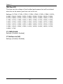
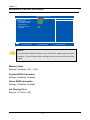
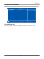
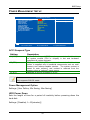
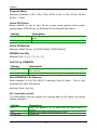
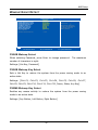
User’s Manual
EPIA-PX
Version 1.20
June 11, 2008
Copyright
Copyright © 2006-2008 VIA Technologies Incorporated. All rights reserved.
No part of this document may be reproduced, transmitted, transcribed, stored in a retrieval
system, or translated into any language, in any form or by any means, electronic, mechanical,
magnetic, optical, chemical, manual or otherwise without the prior written permission of VIA
Technologies, Incorporated.
Trademarks
All trademarks are the property of their respective holders. PS/2 is a registered trademark of
IBM Corporation. Award BIOS is a registered trademark of Phoenix Technologies Ltd.
Macrovision
Apparatus Claims of U.S. Patent Nos. 6,836,549; 6,381,747; 7,050,698; 6,516,132; 5,583,936
licensed for limited viewing uses only.
This product incorporates copyright protection
technology that is protected by certain U.S. patents and other intellectual property rights owned
by Macrovision and other rights owners. Use of this copyright protection technology must be
authorized by Macrovision, and is intended for home and other limited viewing uses only
unless otherwise authorized by Macrovision.
Reverse engineering or disassembly is
prohibited.
Disclaimer
No license is granted, implied or otherwise, under any patent or patent rights of VIA
Technologies. VIA Technologies makes no warranties, implied or otherwise, in regard to this
document and to the products described in this document. The information provided in this
document is believed to be accurate and reliable as of the publication date of this document.
However, VIA Technologies assumes no responsibility for the use or misuse of the information
in this document and for any patent infringements that may arise from the use of this
document. The information and product specifications within this document are subject to
change at any time, without notice and without obligation to notify any person of such change.
FCC-B Radio Frequency Interference Statement
This equipment has been tested and found to comply with the limits for a class B digital
device, pursuant to part 15 of the FCC rules. These limits are designed to provide reasonable
protection against harmful interference when the equipment is operated in a commercial
environment. This equipment generates, uses and can radiate radio frequency energy and, if not
installed and used in accordance with the instruction manual, may cause harmful interference
to radio communications. Operation of this equipment in a residential area is likely to cause
harmful interference, in which case the user will be required to correct the interference at his
personal expense.
Notice 1
The changes or modifications not expressly approved by the party responsible for compliance
could void the user's authority to operate the equipment.
Notice 2
Shielded interface cables and A.C. power cord, if any, must be used in order to comply with
the emission limits.
Tested To Comply
With FCC Standards
FOR HOME OR OFFICE USE
Safety Instructions
1.
Always read the safety instructions carefully.
2.
Keep this User's Manual for future reference.
3.
Keep this equipment away from humidity.
4.
Lay this equipment on a reliable flat surface before setting it up.
5.
The openings on the enclosure are for air convection hence protects the equipment from
overheating. DO NOT COVER THE OPENINGS.
6.
Make sure the voltage of the power source and adjust properly 110/220V before
connecting the equipment to the power inlet.
7.
Place the power cord in such a way that people cannot step on it. Do not place anything
over the power cord.
8.
Always unplug the power cord before inserting any add-on card or module.
9.
All cautions and warnings on the equipment should be noted.
10. Never pour any liquid into the opening. Liquid can cause damage or electrical shock.
11. If any of the following situations arises, get the equipment checked by a service personnel:
•
The power cord or plug is damaged
•
Liquid has penetrated into the equipment
•
The equipment has been exposed to moisture
•
The equipment has not work well or you cannot get it work according to User's
•
The equipment has dropped and damaged
•
If the equipment has obvious sign of breakage
Manual.
12. DO NOT LEAVE THIS EQUIPMENT IN AN ENVIRONMENT UNCONDITIONED,
OR STORAGE TEMPERATURE ABOVE 60oC (140oF), THE EQUIPMENT MAY BE
DAMAGED.
Caution:
Only use the appropriate battery specified for this product.
Do not reuse, recharge, or reheat an old battery.
Do not attempt to force open the battery.
Do not discard used batteries with regular trash.
Discard used batteries according to local regulations.
B OX C ONTENTS
One
One
One
One
One
One
One
Two
EPIA PX Pico-ITX Mainboard
ATA-133/100/66 IDE Ribbon Cable
PS/2 Ribbon Cable
Power Ribbon Cable
COM Port Ribbon Cable
DVI Ribbon Cable
Driver Utility CD
Screws (for the COM port)
i
T ABLE
OF
C ONTENTS
SPECIFICATIONS ............................................................................ 1
M AINBOARD S PECIFICATIONS ............................................................. 2
M AINBOARD L AYOUT ........................................................................ 4
B ACK P ANEL L AYOUT ....................................................................... 4
INSTALLATION ............................................................................... 5
CPU ................................................................................................ 6
CPU Fan: CPU_FAN .................................................................... 6
M EMORY M ODULE I NSTALLATION ...................................................... 7
Memory Slot: DDR2_SODIMM ...................................................... 7
Available DDR2 SDRAM Configurations ........................................ 7
C ONNECTING THE P OWER S UPPLY ...................................................... 8
Pico-ITX 12-Pin Power Connector ................................................. 8
B ACK P ANEL P ORTS .......................................................................... 9
VGA Port...................................................................................... 9
RJ45 LAN Port.............................................................................. 9
C ONNECTORS .................................................................................. 10
IDE Connector: IDE .................................................................. 10
Serial ATA Connectors: SATA..................................................... 11
USB Pin Connector: USB ........................................................... 11
KBMS Connector: PS/2 .............................................................. 11
Case Connector: Front Panel ..................................................... 12
Power Switch (PW_BN) ............................................................... 12
Reset Switch (RST_SW) ............................................................... 12
Power LED (PWR_LED).............................................................. 12
HDD LED (HD_LED).................................................................. 12
Speaker (SPEAK) ........................................................................ 12
Audio Connector: AUDIO ........................................................... 13
Serial Port Connector: COM Port ............................................... 13
LVDS/DVI Panel Connector: LVDS Panel ................................... 14
Multimedia Connector ................................................................. 16
J UMPERS ........................................................................................ 17
Clear CMOS: CMOS Reset .......................................................... 17
ii
BIOS SETUP .................................................................................... 19
E NTERING S ETUP ............................................................................ 20
C ONTROL K EYS .............................................................................. 21
N AVIGATING THE BIOS M ENUS ........................................................ 22
G ETTING H ELP ................................................................................ 23
M AIN M ENU ................................................................................... 24
Standard CMOS Features ............................................................ 24
Advanced BIOS Features ............................................................. 24
Advanced Chipset Features.......................................................... 24
Integrated Peripherals ................................................................ 24
Power Management Setup ............................................................ 24
PnP/PCI Configurations .............................................................. 24
Frequency/Voltage Control.......................................................... 24
Load Fail-Safe Defaults .............................................................. 25
Load Optimized Defaults ............................................................. 25
Set Supervisor Password ............................................................. 25
Set User Password ...................................................................... 25
Save & Exit Setup ....................................................................... 25
Exit Without Saving..................................................................... 25
S TANDARD CMOS F EATURES ........................................................... 26
Date ........................................................................................... 26
Time ........................................................................................... 26
Halt On ...................................................................................... 26
Video.......................................................................................... 26
IDE D RIVES .................................................................................... 27
A DVANCED BIOS F EATURES ............................................................ 28
Virus Warning ............................................................................ 28
Quick Power On Self-Test............................................................ 28
First/Second/Third Boot Device ................................................... 29
Boot Other Device....................................................................... 29
Boot Up NumLock Status ............................................................. 29
Typematic Rate Setting ................................................................ 29
Security Option ........................................................................... 30
MPS Variation Control for OS ..................................................... 30
OS Select For DRAM > 64MB...................................................... 30
iii
Full Screen Logo Show ................................................................ 30
CPU F EATURE ................................................................................ 31
Deplay Prior to Thermal ............................................................. 31
Thermal Management .................................................................. 31
TM2 Bus Ratio ............................................................................ 31
TM2 Bus VID .............................................................................. 32
C7 CMPXCHGB .......................................................................... 32
C7 NoExecute (NX) ..................................................................... 32
H ARD D ISK B OOT P RIORITY ............................................................. 33
A DVANCED C HIPSET F EATURES ........................................................ 34
Memory Hole .............................................................................. 34
System BIOS Cacheable............................................................... 34
Video RAM Cacheable ................................................................. 34
Init Display First ........................................................................ 34
Select Display Device .................................................................. 35
Panel Type.................................................................................. 35
AGP & P2P B RIDGE C ONTROL ......................................................... 36
AGP Aperture Size ...................................................................... 36
AGP 2.0 Mode ............................................................................ 36
AGP Driving Control .................................................................. 37
AGP Fast Write........................................................................... 37
AGP Master 1 WS Write .............................................................. 37
AGP Master 1 WS Read ............................................................... 37
AGP 3.0 Calibration Cycle .......................................................... 37
VGA Share Memory Size .............................................................. 37
Direct Frame Buffer .................................................................... 37
CPU & PCI B US C ONTROL ............................................................... 38
PCI Master 0 WS Write ............................................................... 38
PCI Delay Transaction ................................................................ 38
DRDY_Timing ............................................................................. 38
I NTEGRATED P ERIPHERALS .............................................................. 39
Onboard Serial Port.................................................................... 39
VIA O N C HIP PCI D EVICE ................................................................ 40
Azalia HDA Controller ................................................................ 40
LAN Boot ROM ........................................................................... 40
iv
USB D EVICE S ETTING ..................................................................... 41
USB 1.0 Controller ..................................................................... 41
USB 2.0 Controller ..................................................................... 41
USB Operation Mode .................................................................. 41
USB Keyboard Function .............................................................. 42
USB Storage Function ................................................................. 42
No Device ................................................................................... 42
P OWER M ANAGEMENT S ETUP ........................................................... 43
ACPI Suspend Type ..................................................................... 43
Power Management Option .......................................................... 43
HDD Power Down....................................................................... 43
Suspend Mode ............................................................................. 44
Video Off Option ......................................................................... 44
Video Off Method ........................................................................ 44
MODEM Use IRQ ....................................................................... 44
Soft-Off by PWRBTN ................................................................... 44
Run VGABIOS if S3 Resume......................................................... 44
AC Loss Auto restart ................................................................... 44
W AKEUP E VENT D ETECT ................................................................. 45
PS2KB Wakeup Select ................................................................. 45
PS2KB Wakeup Key Select ........................................................... 45
PS2MS Wakeup Key Select........................................................... 45
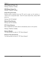
PS2 Keyboard Power On ............................................................. 46
PS2 Mouse Power On .................................................................. 46
PowerOn by PCI Card................................................................. 46
Modem Ring Resume ................................................................... 46
RTC Alarm Resume ..................................................................... 46
Date (of Month) .......................................................................... 46
Resume Time (hh:mm:ss) ............................................................. 46
PNP/PCI C ONFIGURATIONS ............................................................. 47
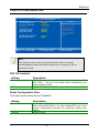
PNP OS Installed ........................................................................ 47
Reset Configuration Data ............................................................ 47
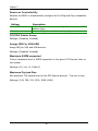
Resource Controlled By ............................................................... 48
PCI/VGA Palette Snoop ............................................................... 48
Assign IRQ For VGA/USB ........................................................... 48
v
Maximum ASPM supported .......................................................... 48
Maximum Payload Size................................................................ 48
F REQUENCY / V OLTAGE C ONTROL .................................................... 49
Auto Detect PCI Clk .................................................................... 49
DRAM C LOCK /D RIVE C ONTROL ....................................................... 50
DRAM Clock ............................................................................... 50
DRAM Timing ............................................................................. 50
Read to Precharge (Trtp) ............................................................ 51
Write to Read CMD (Twtr) .......................................................... 51
Write Recovery Time (Twr) .......................................................... 51
DRAM Command Rate ................................................................. 51
RDSAIT mode ............................................................................. 51
L OAD F AIL -S AFE D EFAULTS ............................................................ 52
L OAD O PTIMIZED D EFAULTS ............................................................ 53
S ET S UPERVISOR / U SER P ASSWORD ................................................. 54
S AVE & E XIT S ETUP ........................................................................ 56
E XIT W ITHOUT S AVING ................................................................... 57
DRIVER INSTALLATION .............................................................. 59
D RIVER U TILITIES ........................................................................... 60
Getting Started ........................................................................... 60
Running the Driver Utilities CD .................................................. 61
CD C ONTENT .................................................................................. 62
vi
CHAPTER 1
Specifications
The ultra-compact and highly integrated VIA EPIA-PX Pico-ITX
mainboard is the smallest form-factor available today. Through a
high level of integration, the Pico-ITX measures at only 25% of
the size of a Mini-ITX mainboard. The mainboard enables the
creation of an exciting new generation of small, ergonomic,
innovative and affordable embedded systems.
1
Chapter 1
M AINBOARD S PECIFICATIONS
CPU
•
Supports VIA C7 1.0GHz NanoBGA2 Processor
Chipset
•
VIA VX700 Advanced All-in-One System Processor
Memory
•
1 x DDR2 533 SODIMM slot (up to 1 GB)
Graphics
•
Integrated UniChrome™ Pro II 3D/2D AGP with MPEG-2/4 and
WMV9 Video Decoding Acceleration
IDE
•
1 x UltraDMA 133/100 connector (2.0mm 40-pin connector)
Serial ATA
•
1 x SATA connector
LAN
•
VIA VT6106S 10/100 Mbps Fast Ethernet Controller with Power
Management Functions
Audio
•
VIA VT1708A High Definition Audio Codec
Back Panel I/O Port
•
1 x RJ-45 LAN Port
•
1 x VGA Port
2
Specifications
Onboard I/O Connectors
•
1 x USB pin connector for 4 additional USB 2.0 ports
•
1 x COM pin connector
•
1 PS2 mouse/keyboard pin connector
•
1 Fan pin connector for CPU Fan
•
1 x LVDS/DVI panel pin connector
•
1 Audio pin connector for Line-in, MIC-in, S/PDIF in, and 5.1
Channels Audio Output
•
1 Multimedia connector to support External TV-Out Interface,
Video Capture Port Interface and Low Pin Count Interface.
(One VT1625M add-on card is required.)
•
1 x Pico-ITX power connector
BIOS
•
Award BIOS with LPC 4/8Mbit flash memory capacity
Form Factor
•
Pico-ITX (10 layers)
•
10 cm X 7.2 cm
3
Chapter 1
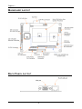
M AINBOARD L AYOUT
B ACK P ANEL L AYOUT
4
CHAPTER 2
Installation
This chapter provides you with information about hardware
installation procedures. It is recommended to use a grounded wrist
strap before handling computer components. Electrostatic discharge
(ESD) can damage some components.
5
Chapter 2
CPU
The VIA EPIA-PX Pico-ITX mainboard can support VIA C7 NanoBGA2
processor. The processor requires a heatsink with fan for 1.0GHz SKU.
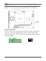
CPU Fan: CPU_FAN
The CPU_FAN runs on +5V and maintain CPU cooling. When connecting the
wire to the connectors, always be aware that the red wire (positive wire)
should be connected to +5V. The black wire is Ground and should always be
connected to GND.
Pin
Signal
1
2
3
FAN OUT
+5V
GND
1
6
Installation
MEMORY MODULE INSTALLATION
Memory Slot: DDR2_SODIMM
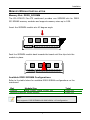
The VIA EPIA-PX Pico-ITX mainboard provides one SODIMM slot for DDR2
533 SDRAM memory modules and supports memory sizes up to 1GB.
Insert the SODIMM module at a 45 degree angle.
Push the SODIMM module back towards the board until the clips lock the
module in place.
Available DDR2 SDRAM Configurations
Refer to the table below for available DDR2 SDRAM configurations on the
mainboard.
Slot
Module Size
Total
SODIMM
64MB, 128MB, 256MB, 512MB, 1GB
Maximum supported system memory
64MB-1GB
64MB-1GB
Note:
Only supports 1GB SODIMM with 64M x 8bits x16 configuration.
7
Chapter 2
CONNECTING THE POWER SUPPLY
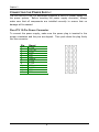
The VIA EPIA-PX Pico-ITX mainboard supports a Pico-ITX power supply for
the power system.
Before inserting the power supply connector, always
make sure that all components are installed correctly to ensure that no
damage will be caused.
Pico-ITX 12-Pin Power Connector
To connect the power supply, make sure the power plug is inserted in the
proper orientation and the pins are aligned. Then push down the plug firmly
into the connector.
Pin
Signal
1
2
3
4
5
6
7
8
9
10
11
12
+3.3V
+5V_SB
+12V
+5V
+5V
PWRGD
+3.3V
+3.3V
GND
PWRON
GND
GND
8
Installation
BACK PANEL PORTS
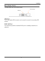
The back panel has the following layout:
VGA Port
The 15-pin female VGA connector can be used to connect to any analog VGA
monitor.
RJ45 LAN Port
The mainboard provides a standard RJ45 port for enabling connections to
networks.
9
Chapter 2
CONNECTORS
IDE Connector: IDE
The mainboard has an Ultra DMA 133/100 controller. You can connect up to
two IDE devices in any combination.
1
44
If two drives are connected to a single cable, the jumper on the second drive
must be set to slave mode. Refer to the drive documentation supplied by the
vendor for the jumper settings.
Pin
Signal
Pin
Signal
1
3
5
7
9
11
13
15
17
19
21
23
25
27
29
31
33
35
37
39
41
43
#IDERST
PDD7
PDD6
PDD5
PDD4
PDD3
PDD2
PDD1
PDD0
GND
PDDREQ
#PDIOW
#PDIOR
PIORDY
#PDDACK
IRQ15
PDA1
PDA0
#PDCS1
#HD_LED1
+5V
GND
2
4
6
8
10
12
14
16
18
20
22
24
26
28
30
32
34
36
38
40
42
44
GND
PDD8
PDD9
PDD10
PDD11
PDD12
PDD13
PDD14
PDD15
NC
GND
GND
GND
GND
GND
NC
GP10
PDA2
#PDCS3
GND
+5V
NC
10
Installation
Serial ATA Connectors: SATA
The next generation connector supports thin Serial ATA cables for
primary internal storage devices. The current Serial ATA interface
allows up to 150MB/s data transfer rate, faster than the standard
parallel ATA with 133 MB/s (Ultra DMA).
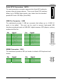
USB Pin Connector: USB
The mainboard provides 1 USB pin connector that allows up to 4 USB 2.0
ports to be added.
This port can be used to connect high-speed USB
interface peripherals such as USB HDD, digital cameras, MP3 players, printers,
modem and the like.
Pin
Signal
Pin
Signal
1
3
5
7
9
11
13
15
GND
GND
+USB_VD2
-USB_VD2
+5V
-USB_VD1
+USB_VD1
GND
2
4
6
8
10
12
14
16
NC
GND
+USB_VD3
-USB_VD3
+5V
-USB_VD0
+USB_VD0
GND
1
2
15
16
KBMS Connector: PS/2
The mainboard provides a PS2 pin header to attach a PS2 keyboard and
mouse.
Pin
Signal
Pin
Signal
1
3
5
A5V
KBCLK
MSCLK
2
4
6
GND
KBDATA
MSDATA
11
1
2
5
6
Chapter 2
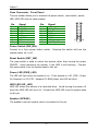
Case Connector: Front Panel
This pin header allows you to connect the power switch, reset switch, power
LED, HDD LED and the case speaker.
Pin
Signal
Pin
Signal
1
3
5
7
9
11
13
15
PW_LED
PW_LED
SUS_LED
+5V
GND
#EXTSMI
SPEAK
NC
2
4
6
8
10
12
14
16
+5V
HDD_LED
PW_BN
GND
RST_SW
GND
+5V
#SLEEP_LED
1
2
15
16
Power Switch (PW_BN)
Connect to a 2-pin power button switch. Pressing this button will turn the
system power on or off.
Reset Switch (RST_SW)
The reset switch is used to reboot the system rather than turning the power
ON/OFF. Avoid rebooting the system, if the HDD is still working. Connect
the reset switch from the system case to this pin.
Power LED (PWR_LED)
The LED will light when the system is on. If the system is in S1 (POS - Power
On Suspend) or S3 (STR - Suspend To RAM) state, the LED will blink.
HDD LED (HD_LED)
HDD LED shows the activity of a hard disk drive. Avoid turning the power off
when the HDD LED still has a lit. Connect the HDD LED from the system case
to this pin.
Speaker (SPEAK)
The speaker from the system case is connected to this pin.
12
Installation
Audio Connector: AUDIO
This is an interface for connections to external audio devices.
Pin
Signal
Pin
Signal
1
3
5
7
9
11
13
15
17
LINE IN R
LINE IN L
LINEOUT_R
LINEOUT_L
SURROUT R
SENSE_A
CEN_OUT
SSROUT_R
SPDIF_IN
2
4
6
8
10
12
14
16
18
AGND
+5V
MIC IN L
MIC IN R
SURROUT L
SENSE_B
LFE_OUT
SSROUT_L
GND
1
17
2
18
Serial Port Connector: COM Port
COM port pin header can be used to attach additional ports for serial mouse
or other serial devices.
Pin
Signal
Pin
Signal
1
2
3
4
5
#DCDA
RXDA
TXDA
#DTRA
GND
6
7
8
9
10
#DSRA
#RTSA
#CTSA
#RIA
NC
13
6
1
9
5
Chapter 2
LVDS/DVI Panel Connector: LVDS Panel
The LVDS/DVI Panel connector allows you to connect the panel’s LVDS cable
directly to support LVDS panel without any need of a daughter card.
Connector: ACES 87216-4016 (2x20 pins / 1.0mm)
Matching Connector: ACES 87219-4000
Pin
Signal
Pin
Signal
1
3
5
7
9
11
13
15
17
19
21
23
25
27
29
31
33
35
37
39
+12V
+12V
-LCD1_D2
+LCD1_D2
+12V
-LCD2_CLK
+LCD2_CLK
+5V
-LCD2_D3
+LCD2_D3
+5V
+LCD2_D2
-LCD2_D2
GND
+LCD2_D1
-LCD2_D1
GND
ENAVDD1
ENAVDD2
GND
2
4
6
8
10
12
14
16
18
20
22
24
26
28
30
32
34
36
38
40
+LCD1_D0
-LCD1_D0
+3V
+LCD1_D1
-LCD1_D1
+3V
-LCD1_CLK
+LCD1_CLK
+3V
-LCD1_D3
+LCD1_D3
GND
+LCD2_D0
-LCD2_D0
GND
SPD1
SPCLK1
ENABLT2
ENABLT1
GND
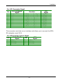
For DVI Connector Signal
DVI Connector
Pin
Signal
2
4
5
7
8
10
14
16
32
34
TXC+
TXCTX1TX1+
TX0+
TX0TX2TX2+
I²C Data
I²C Clock
CN5
Signal
+LCD1_D0
-LCD1_D0
-LCD1_D2
+LCD1_D2
+LCD1_D1
-LCD1_D1
-LCD1_CLK
+LCD1_CLK
SPD1
SPCLK1
14
1
2
39
40
Installation
For LCD Connector Signal
LCD Connector
Pin
Signal
11
13
17
19
23
25
26
28
29
31
RxCLKRxCLK+
Rx3Rx3+
Rx2+
Rx2Rx0+
Rx0Rx1+
Rx1-
Function
-LVDS Receiver Clock Signal
+LVDS Receiver Clock Signal
-LVDS Receiver Signal
+LVDS Receiver Signal
+LVDS Receiver Signal
-LVDS Receiver Signal
+LVDS Receiver Signal
-LVDS Receiver Signal
+LVDS Receiver Signal
-LVDS Receiver Signal
CN5
Signal
-LCD2_CLK
+LCD2_CLK
-LCD2_D3
+LCD2_D3
+LCD2_D2
-LCD2_D2
+LCD2_D0
-LCD2_D0
+LCD2_D1
-LCD2_D1
This connector work also as an interface and allows you to connect the EPIA
PX’s daughter card, PX-O.
For LCD Inverter Control Signal
PX-O (CN10)
Pin
Pin
Signal
6
7
8
9
SPD1
SPCLK1
ENAVDD2
ENABLT2
32
34
37
36
CN5
Signal
SPD1
SPCLK1
ENAVDD2
ENABLT2
15
Chapter 2
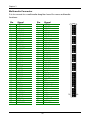
Multimedia Connector
It is to connect to a multimedia daughter board for more multimedia
functions.
Pin
Signal
Pin
Signal
1
3
5
7
9
11
13
15
17
19
21
23
25
27
29
31
33
35
37
39
41
43
45
47
49
51
53
55
57
59
61
63
65
67
69
71
73
75
77
79
HTVD2
+5V
+5V
HTVD12
HTVD14
CAPD13
CAPD12
GND
CAPD14
TS1ERR
CAPD11
CAPHS1
#PCIRST1
CAPD8
GND
CAPCLK1
CAPD1
CAPD0
CAPD6
CAPHS
GND
SMBDT
SMBCK
HTVD5
HTVD9
CAPD3
CAPD7
CAPCLK
CAPD4
GND
GPIO2
CAPD5
CAPV3
GPIO3
#SIOSMI
#LDRQ1
LAD1
SERIRQ
GND
SIOOSC2
2
4
6
8
10
12
14
16
18
20
22
24
26
28
30
32
34
36
38
40
42
44
46
48
50
52
54
56
58
60
62
64
66
68
70
72
74
76
78
80
HTVD8
HTVD7
HTVD10
+5V
HTVD6
HTVD4
HTVCLKR
+5V
DVP1DET
HTVVS
HTVD0
HTVHS
HTVD1
HTVD13
CAPVS1
CAPD9
CAPD10
CAPD15
DVP0DE
HTVDE
HTVD15
HTVD3
HTVD11
CAPD2
GND
HTVCLK
SPDIF_OUT
HTVFLD
SPD1
SPCLK1
DISPCLKO1
DISPCLKI1
+3V
+3V
+3V
LAD2
LAD3
#LFRAME
LAD0
PCLKLPC
16
1
79
2
80
Installation
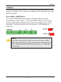
JUMPERS
The mainboard provides jumpers for setting some mainboard functions. This
section will explain how to change the settings of the mainboard functions
using the jumpers.
Clear CMOS: CMOS Reset
The onboard CMOS RAM stores system configuration data and has an
onboard battery power supply. To reset the CMOS settings, set the jumper
on pins 2 and 3 while the system is off. Return the jumper to pins 1 and 2
afterwards. Setting the jumper while the system is on will damage the
mainboard.
Setting
1
2
3
Normal Operation
Clear CMOS setting
ON
OFF
ON
ON
OFF
ON
Normal:
1 2
Clear:
1
2 3
Caution:
Except when clearing the RTC RAM, never remove the cap on CMOS
Reset jumper default position. Removing the cap will cause system boot
failure. Avoid clearing the CMOS while the system is on; it will damage
the mainboard.
17
3
CHAPTER 3
BIOS Setup
This chapter gives a detailed explanation of the BIOS setup functions.
19
Chapter 3
ENTERING SETUP
Power on the computer and press <Delete> during the beginning of the boot
sequence to enter the BIOS setup menu. If you missed the BIOS setup entry
point, you may restart the system and try again.
20
BIOS Setup
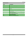
CONTROL KEYS
Keys
Description
Up Arrow
Down Arrow
Left Arrow
Right Arrow
Enter
Escape
Move to the previous item
Move to the next item
Move to the item in the left side
Move to the item in the right side
Select the item
Jumps to the Exit menu or returns to the main menu from a
submenu
Increase the numeric value or make changes
Decrease the numeric value or make changes
General help, only for Status Page Setup Menu and Option
Page Setup Menu
Restore the previous CMOS value from CMOS, only for
Option Page Setup Menu
Load the default CMOS value from Fail-Safe default table,
only for Option Page Setup Menu
Load Optimized defaults
Jumps to the Main Menu
Save all the CMOS changes and exit
Page Up / +
Page Down / F1
F5
F6
F7
F9
F10
21
Chapter 3
NAVIGATING THE BIOS MENUS
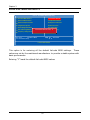
The main menu displays all the BIOS setup categories. Use the Up/Down/
Left/Right arrow keys to select any item or sub-menu.
Description of the
selected/highlighted category is displayed at the bottom of the screen.
An arrow symbol next to a field indicates that a sub-menu is available (see
figure below).
Press <Enter> to display the sub-menu.
menu, press <Esc>.
22
To exit the sub-
BIOS Setup
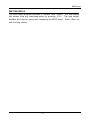
GETTING HELP
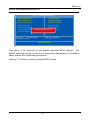
The BIOS setup program provides a “General Help” screen. You can display
this screen from any menu/sub-menu by pressing <F1>.
The help screen
displays the keys for using and navigating the BIOS setup. Press <Esc> to
exit the help screen.
23
Chapter 3
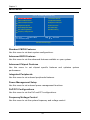
MAIN MENU
Phoenix - AwardBIOS CMOS Setup Utility
Standard CMOS Features
Load Fail-Safe Defaults
Advanced BIOS Features
Load Optimized Defaults
Advanced Chipset Features
Set Supervisor Password
Integrated Peripherals
Set User Password
Power Management Setup
Save & Exit Setup
PnP / PCI Configurations
Exit Without Saving
Frequency / Voltage Control
Esc : Quit
F9 : Menu in BIOS
: Select Item
F10 : Save & Exit Setup
Time, Date, Hard Disk Type...
Standard CMOS Features
Use this menu to set basic system configurations.
Advanced BIOS Features
Use this menu to set the advanced features available on your system.
Advanced Chipset Features
Use this menu to set chipset specific features and optimize system
performance.
Integrated Peripherals
Use this menu to set onboard peripherals features.
Power Management Setup
Use this menu to set onboard power management functions.
PnP/PCI Configurations
Use this menu to set the PnP and PCI configurations.
Frequency/Voltage Control
Use this menu to set the system frequency and voltage control.
24
BIOS Setup
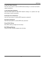
Load Fail-Safe Defaults
Use this menu option to load the BIOS default settings for minimal and stable
system operations.
Load Optimized Defaults
Use this menu option to load BIOS default settings for optimal and high
performance system operations.
Set Supervisor Password
Use this menu option to set the BIOS supervisor password.
Set User Password
Use this menu option to set the BIOS user password.
Save & Exit Setup
Save BIOS setting changes and exit setup.
Exit Without Saving
Discard all BIOS setting changes and exit setup.
25
Chapter 3
STANDARD CMOS FEATURES
Phoenix - AwardBIOS CMOS Setup Utility
Standard CMOS Features
Date (mm:dd:yy)
Time (hh:mm:ss)
Tue, Jul 13 1999
11 : 20 : 55
IDE Channel 0 Master
IDE Channel 0 Slave
IDE Channel 1 Master
IDE Channel 1 Slave
Change the day, month, year
and century
Video
Halt On
[EGA/VGA]
[All , But Keyboard]
Base Memory
Extended Memory
Total Memory
: Move
Item Help
Menu Level
640K
15360K
16384K
Enter: Select
+/-/PU/PD: Value
F5: Previous Values
F10: Save
F6: Fail-Safe Defaults
ESC: Exit
F1: General Help
F7: Optimized Defaults
Date
The date format is [Day, Month Date Year]
Time
The time format is [Hour : Minute : Second]
Halt On
Sets the system’s response to specific boot errors.
Below is a table that
details the possible settings.
Setting
Description
All Errors
No Errors
All, But Keyboard
System halts when any error is detected
System does not halt for any error
System halts for all non-key errors
Video
Settings: [EGA/VGA, CGA 40, CGA 80, MONO]
26
BIOS Setup
IDE DRIVES
Phoenix - AwardBIOS CMOS Setup Utility
IDE Channel 0 Master
IDE HDD Auto-Detection
[Press Enter]
IDE Channel 0 Master
Access Mode
[Auto]
[Auto]
Capacity
0 MB
Cylinder
Head
Precomp
Landing Zone
Sector
0
0
0
0
0
: Move
Enter: Select
F5: Previous Values
Item Help
Menu Level
To auto-detect the HDD's size,
head... on this channel
+/-/PU/PD: Value
F10: Save
F6: Fail-Safe Defaults
ESC: Exit
F1: General Help
F7: Optimized Defaults
The specifications of your drive must match with the drive table. The hard
disk will not work properly if you enter incorrect information in this category.
Select “Auto” whenever possible.
If you select “Manual”, make sure the
information is from your hard disk vendor or system manufacturer. Below is
a table that details required hard drive information when using the “Manual”
mode.
Setting
Description
IDE Channel
The name of this match the name of the menu. Settings:
[None, Auto, Manual]
Settings: [CHS, LBA, Large, Auto]
Formatted size of the storage device
Number of cylinders
Number of heads
Write precompensation
Cylinder location of the landing zone
Number of sectors
Access Mode
Capacity
Cylinder
Head
Precomp
Landing Zone
Sector
27
Chapter 3
ADVANCED BIOS FEATURES
Phoenix - AwardBIOS CMOS Setup Utility
Advanced BIOS Features
CPU Feature
Hard Disk Boot Priority
Virus Warning
Quick Power On Self Test
First Boot Device
Second Boot Device
Third Boot Device
Boot Other Device
Boot Up NumLock Status
Typematic Rate Setting
Typematic Rate (Chars/Sec)
Typematic Delay (Msec)
Security Option
MPS Version Control For OS
OS Select For DRAM > 64MB
Full Screen LOGO Show
: Move
Enter: Select
[Press Enter]
[Press Enter]
[Disabled]
[Enabled]
[CDROM]
[Hard Disk]
[LS120]
[Enabled]
[On]
[Disabled]
6
250
[Setup]
[1.4]
[Non-OS2]
[Enabled]
+/-/PU/PD: Value
F5: Previous Values
Item Help
Menu Level
F10: Save
F6: Fail-Safe Defaults
ESC: Exit
F1: General Help
F7: Optimized Defaults
Virus Warning
Setting
Description
Enabled
Disabled
Turns on hard disk boot sector virus protection
Turns off hard disk boot sector virus protection
Quick Power On Self-Test
Shortens Power On Self-Test (POST) cycle to enable shorter boot up time.
Setting
Description
Enabled
Disabled
Shorten Power On Self Test (POST) cycle and bootup time
Standard Power On Self Test (POST)
28
BIOS Setup
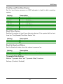
First/Second/Third Boot Device
Set the boot device sequence as BIOS attempts to load the disk operating
system.
Setting
Description
LS120
Hard Disk
CD-ROM
ZIP100
USB-FDD
USB-ZIP
USB-CDROM
Legacy LAN
Disabled
Boot from LS-120 drive
Boot from the HDD
Boot from CD-ROM
Boot from ATAPI ZIP drive
Boot from USB floppy drive
Boot from USB ZIP drive
Boot from USB CDROM
Boot from network drive
Disable the boot device sequence
Boot Other Device
Enables the system to boot from alternate devices if the system fails to boot
from the “First/Second/Third Boot Device” list.
Setting
Description
Enabled
Disabled
Enable alternate boot device
No alternate boot device allowed
Boot Up NumLock Status
Set the NumLock status when the system is powered on.
Setting
Description
On
Off
Forces keypad to behave as 10-key
Forces keypad to behave as arrow keys
Typematic Rate Setting
Enables “Typematic Rate” and “Typematic Delay” functions.
Settings: [Enabled, Disabled]
29
Chapter 3
Security Option
Selects whether the password is required every time the System boots, or
only when you enter Setup.
Setting
Description
Setup
Password prompt appears only when end users try to run BIOS
Setup
Password prompt appears every time when the computer is
powered on and when end users try to run BIOS Setup
System
MPS Variation Control for OS
Settings: [1.1, 1.4]
OS Select For DRAM > 64MB
Select OS2 only if you are running OS/2 operating system with greater than
64MB of RAM on the system.
Settings: [Non-OS2, OS2]
Full Screen Logo Show
Show full screen logo during BIOS boot up process.
Settings: [Enabled, Disabled]
30
BIOS Setup
CPU FEATURE
Phoenix - AwardBIOS CMOS Setup Utility
CPU Feature
[16 Min]
[Thermal Monitor 1]
[ 0 X]
[0.700V]
[Enabled]
[Disabled]
Deplay Prior to Thermal
Thermal Management
TM2 Bus Ratio
TM2 Bus VID
C7 CMPXCHGB
C7 NoExecute (NX)
: Move
Enter: Select
+/-/PU/PD: Value
F5: Previous Values
F10: Save
F6: Fail-Safe Defaults
Item Help
Menu Level
ESC: Exit
F1: General Help
F7: Optimized Defaults
Deplay Prior to Thermal
Settings: [4 Min, 8 Min, 16 Min, 32 Min]
Thermal Management
This item sets CPU’s thermal control rule to protect CPU from overheat.
Setting
Description
Thermal Monitor 1
Thermal Monitor 2
On-die throtting
Ratio & VID transition
TM2 Bus Ratio
This item sets the frequency (bus ratio) of the throttled performance that will
be initiated when the on die sensor goes from not hot to hot.
Key in a DEC number.
Settings: [Min = 0, Max = 255]
31
Chapter 3
TM2 Bus VID
This item sets the voltage of the throttled performance that will be initiated
when the on die sensor goes from not hot to hot.
Settings: [0.700V, 0.716V, 0.732V, 0.748V, 0.764V, 0.780V, 0.796V, 0.812V,
0.828V, 0.844V, 0.860V, 0.876V, 0.892V, 0.908V, 0.924V, 0.940V, 0.956V,
0.972V, 0.988V, 1.004V, 1.020V, 1.036V, 1.052V, 1.068V, 1.084V, 1.100V,
1.116V, 1.132V, 1.148V, 1.164V, 1.180V, 1.196V, 1.212V, 1.228V, 1.244V,
1.260V, 1.276V, 1.292V, 1.308V, 1.324V, 1.340V, 1.356V, 1.372V, 1.388V,
1.404V, 1.420V, 1.436V, 1.452V, 1.468V, 1.484V, 1.500V, 1.516V, 1.532V,
1.548V, 1.564V, 1.580V, 1.596V, 1.612V, 1.628V, 1.644V, 1.660V, 1.676V,
1.692V, 1.708]
C7 CMPXCHGB
Settings: [Enabled, Disabled]
C7 NoExecute (NX)
Settings: [Enabled, Disabled]
32
BIOS Setup
HARD DISK BOOT PRIORITY
Phoenix - AwardBIOS CMOS Setup Utility
Hard Disk Boot Priority
1.
2.
3.
4.
5.
6.
7.
8.
Item Help
Pri. Master :
Pri. Slave :
Sec. Master :
Sec. Slave :
USBHDD0 :
USBHDD1 :
USBHDD2 :
Bootable Add-In Cards
Menu Level
Use < > or < > to
select a device, then
press < + > to move it
up, or < - > to move it
down the list. Press
<ESC> to exit this
menu.
: Move
PU/PD/+/-:Change Priority
F5: Previous Values
F6: Fail-Safe Defaults
ESC: Exit
F10: Save
F7: Optimized Defaults
This is for setting the priority of the hard disk boot order when the “Hard
Disk” option is selected in the “[First/Second/Third] Boot Device” menu item.
33
Chapter 3
ADVANCED CHIPSET FEATURES
Phoenix - AwardBIOS CMOS Setup Utility
Advanced Chipset Features
AGP & P2P Bridge Control
CPU & PCI Bus Control
Memory Hole
System BIOS Cacheable
Video RAM Cacheable
Init Display First
[Press Enter]
[Press Enter]
[Disabled]
[Enabled]
[Disabled]
[PCI Slot]
Select Display Device
Panel Type
[CRT]
[02]
: Move
Enter: Select
+/-/PU/PD: Value
F5: Previous Values
Item Help
Menu Level
F10: Save
F6: Fail-Safe Defaults
ESC: Exit
F1: General Help
F7: Optimized Defaults
Caution:
The Advanced Chipset Features menu is used for optimizing the chipset
functions. Do not change these settings unless you are familiar with the
chipset.
Memory Hole
Settings: [Disabled, 15M – 16M]
System BIOS Cacheable
Settings: [Disabled, Enabled]
Video RAM Cacheable
Settings: [Disabled, Enabled]
Init Display First
Settings: [PCI Slot, AGP]
34
BIOS Setup
Select Display Device
This setting refers to the type of display being used with the system.
Settings: [CRT, LCD, CRT+LCD, TV, LCD+TV]
Panel Type
This setting refers to the native resolution of the display being used with the
system.
Key in a HEX number.
Settings: [Min = 0000, Max = 000F]
35
Chapter 3
AGP & P2P BRIDGE CONTROL
Phoenix - AwardBIOS CMOS Setup Utility
AGP & P2P Bridge Control
AGP Aperture Size
AGP 2.0 Mode
AGP Driving Control
x AGP Driving Value
AGP Fast Write
AGP Master 1 WS Write
AGP Master 1 WS Read
AGP 3.0 Calibration cycle
VGA Share Memory Size
Direct Frame Buffer
: Move
Enter: Select
F5: Previous Values
[128M]
[4x]
[Auto]
DA
[Disabled]
[Enabled]
[Enabled]
[Enabled]
[64M]
[Enabled]
+/-/PU/PD: Value
Item Help
Menu Level
F10: Save
F6: Fail-Safe Defaults
ESC: Exit
F1: General Help
F7: Optimized Defaults
AGP Aperture Size
This setting controls how much memory space can be allocated to AGP for
video purposes. The aperture is a portion of the PCI memory address range
dedicated to graphics memory address space.
Host cycles that hit the
aperture range are forwarded to the AGP without any translation.
Settings: [32MB, 64MB, 128MB, 256MB, 512MB, 1G]
AGP 2.0 Mode
This mainboard supports the AGP 4x interface. When the AGP 4x video card
is used, it can transfer video data at 1066MB/s. AGP 4x is backward
compatible, leave the default 4x mode on. AGP 4x mode can be detected
automatically once you plug in the AGP 4x card.
Settings: [4x, 2x, 1x]
36
BIOS Setup
AGP Driving Control
This item is used to signal driving current on AGP cards to auto or manual.
Settings: [Auto, Manual]
AGP Fast Write
This item is used to enable or disable the caching of display data for the
video memory of the processor.
Settings: [Enabled, Disabled]
AGP Master 1 WS Write
Settings: [Enabled, Disabled]
AGP Master 1 WS Read
Settings: [Enabled, Disabled]
AGP 3.0 Calibration Cycle
Settings: [Enabled, Disabled]
VGA Share Memory Size
Settings: [Disabled, 32M, 64M, 128M]
Direct Frame Buffer
Settings: [Enabled, Disabled]
37
Chapter 3
CPU & PCI BUS CONTROL
Phoenix - AwardBIOS CMOS Setup Utility
CPU & PCI Bus Control
PCI Master 0 WS Write
PCI Delay Transaction
DRDY_Timing
: Move
Enter: Select
[Enabled]
[Enabled]
[Optimize]
+/-/PU/PD: Value
F5: Previous Values
Item Help
Menu Level
F10: Save
F6: Fail-Safe Defaults
PCI Master 0 WS Write
Settings: [Enabled, Disabled]
PCI Delay Transaction
Settings: [Enabled, Disabled]
DRDY_Timing
Settings: [Slowest, Default, Optimize]
38
ESC: Exit
F1: General Help
F7: Optimized Defaults
BIOS Setup
INTEGRATED PERIPHERALS
Phoenix - AwardBIOS CMOS Setup Utility
Integrated Peripherals
VIA OnChip PCI Device
Onboard Serial Port
USB Device Setting
: Move
Enter: Select
F5: Previous Values
[Press Enter]
[3F8 / IRQ4]
[Press Enter]
+/-/PU/PD: Value
Item Help
Menu Level
F10: Save
F6: Fail-Safe Defaults
ESC: Exit
F1: General Help
F7: Optimized Defaults
Onboard Serial Port
Settings: [Disabled, 3F8/IRQ4, 2F8/IRQ3, 3E8/IRQ4, 2E8/IRQ3, Auto]
39
Chapter 3
VIA ONCHIP PCI DEVICE
Phoenix - AwardBIOS CMOS Setup Utility
VIA OnChip PCI Device
Azalia HDA Controller
LAN Boot ROM
: Move
Enter: Select
F5: Previous Values
[Auto]
[Enabled]
+/-/PU/PD: Value
F10: Save
F6: Fail-Safe Defaults
Azalia HDA Controller
Settings: [Auto, Disabled]
LAN Boot ROM
Settings: [Enabled, Disabled]
40
Item Help
Menu Level
ESC: Exit
F1: General Help
F7: Optimized Defaults
BIOS Setup
USB DEVICE SETTING
Phoenix - AwardBIOS CMOS Setup Utility
USB Device Setting
USB 1.0 Controller
USB 2.0 Controller
USB Operation Mode
USB Keyboard Function
USB Storage Function
[Enabled]
[Enabled]
[High Speed]
[Enabled]
[Enabled]
*** USB Mass Storage Device Boot Setting ***
UFDDA
USB Floppy
UFDDB
USB Floppy
No Device
[Auto mode]
No Device
[Auto mode]
No Device
[Auto mode]
No Device
[Auto mode]
No Device
[Auto mode]
No Device
[Auto mode]
No Device
[Auto mode]
No Device
[Auto mode]
: Move
Enter: Select
F5: Previous Values
+/-/PU/PD: Value
F10: Save
F6: Fail-Safe Defaults
Item Help
Menu Level
[Enable] or [Disable]
Universal Host
Controller
Interface for Universal
Serial Bus
ESC: Exit
F1: General Help
F7: Optimized Defaults
USB 1.0 Controller
Enable or disable Universal Host Controller Interface for Universal Serial Bus.
Settings: [Enabled, Disabled]
USB 2.0 Controller
Enable or disable Enhanced Host Controller Interface for Universal Serial Bus.
Settings: [Enabled, Disabled]
USB Operation Mode
Auto decide USB device operation mode.
Setting
Description
High Speed
If USB device was high speed device, then it operated on high
speed mode. If USB device was full/low speed device, then it
operated on full/low speed mode.
All of USB Device operated on full/low speed mode
Full/Low Speed
41
Chapter 3
USB Keyboard Function
Enable or disable Legacy support of USB Keyboard
Settings: [Enabled, Disabled]
USB Storage Function
Enable or disable Legacy support of USB Mass Storage
Settings: [Enabled, Disabled]
No Device
Setting
Description
Auto mode
FDD mode
HDD mode
According to contents of USB MSD decide boot up type.
The USB MSD always boot up as floppy disk.
The USB MSD always boot up as hard disc.
42
BIOS Setup
POWER MANAGEMENT SETUP
Phoenix - AwardBIOS CMOS Setup Utility
Power Management Setup
ACPI Suspend Type
Power Management Option
HDD Power Down
Suspend Mode
Video Off Option
Video Off Method
MODEM Use IRQ
Soft-Off by PWRBTN
Run VGABIOS if S3 Resume
Ac Loss Auto Restart
Wakeup Event Detect
: Move
Enter: Select
F5: Previous Values
[S1&S3]
[User Define]
[Disabled]
[Disabled]
[Suspend -> Off]
[V/H SYNC+Blank]
[3]
[Instant-Off]
[Auto]
[Off]
[Press Enter]
+/-/PU/PD: Value
F10: Save
F6: Fail-Safe Defaults
Item Help
Menu Level
ESC: Exit
F1: General Help
F7: Optimized Defaults
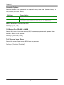
ACPI Suspend Type
Setting
Description
S1(POS)
S1/Power On Suspend (POS) is a low power state. In this state,
no system context (CPU or chipset) is lost and hardware
maintains all system contexts.
S3/Suspend To RAM (STR) is a power-down state. In this state,
power is supplied only to essential components such as main
memory and wakeup-capable devices. The system context is
saved to main memory, and context is restored from the
memory when a "wakeup" event occurs.
Depends on the OS to select S1 or S3.
S3(STR)
S1 & S3
Note:
Only supports S/W S3 mode.
Power Management Option
Settings: [User Define, Min Saving, Max Saving]
HDD Power Down
Sets the length of time for a period of inactivity before powering down the
hard disk.
Settings: [Disabled, 1~15(minutes)]
43
Chapter 3
Suspend Mode
Settings: [Disabled, 1 Min, 2 Min, 4 Min, 6 Min, 8 Min, 10 Min, 20 Min, 30 Min,
40 Min, 1 Hour]
Video Off Option
Select whether or not to turn off the screen when system enters power
saving mode, ACPI OS such as Windows XP will override this option.
Setting
Description
Always On
Screen is always on even when system enters power saving
mode
Screen is turned off when system enters power saving mode
Suspend -> Off
Video Off Method
Settings: [Blank Screen, V/H SYNC+Blank, DPMS Support]
MODEM Use IRQ
Settings: [NA, 3, 4, 5, 7, 9, 10, 11]
Soft-Off by PWRBTN
Setting
Description
Delay 4 Sec
System is turned off if power button is pressed for more than
four seconds
Power button functions as a normal power-on/-off button
Instant-Off
Run VGABIOS if S3 Resume
Select whether to run VGA BIOS if resuming from S3 state.
This is only
necessary for older VGA drivers.
Settings: [Auto, Yes, No]
AC Loss Auto restart
The field defines how the system will respond after an AC power loss during
system operation.
Setting
Description
Off
Keeps the system in an off state until the power button is
pressed
Restarts the system when the power is back
Former-Sts
On
Former-Sts
44
BIOS Setup
WAKEUP EVENT DETECT
Phoenix - AwardBIOS CMOS Setup Utility
Wakeup Event Detect
[Hot Key]
[Any Key]
[Any Botton]
[Disabled]
[Disabled]
[By OS]
[By OS]
[Disabled]
0
0: 0: 0
PS2KB Wakeup Select
PS2KB Wakeup Key Select
PS2MS Wakeup Key Select
PS2 Keyboard Power On
PS2 Mouse Power On
PowerOn by PCI Card
Modem Ring Resume
RTC Alarm Resume
Date (of Month)
Resume Time (hh:mm:ss)
: Move
Enter: Select
+/-/PU/PD: Value
F5: Previous Values
F10: Save
F6: Fail-Safe Defaults
Item Help
Menu Level
When Select Password,
Please press ENTER key
to change Password
Max 8 numbers.
ESC: Exit
F1: General Help
F7: Optimized Defaults
PS2KB Wakeup Select
When selecting Password, press Enter to change password. The maximum
number of characters is eight.
Settings: [Hot Key, Password]
PS2KB Wakeup Key Select
Sets a Hot Key to restore the system from the power saving mode to an
active state.
Settings: [Ctrl+F1, Ctrl+F2, Ctrl+F3, Ctrl+F4, Ctrl+F5, Ctrl+F6, Ctrl+F7,
Ctrl+F8, Ctrl+F9, Ctrl+F10, Ctrl+F11, Ctrl+F12, Power, Wake, Any Key]
PS2MS Wakeup Key Select
Enables any mouse activity to restore the system from the power saving
mode to an active state.
Settings: [Any Button, Left Button, Right Button]
45
Chapter 3
PS2 Keyboard Power On
Settings: [Disabled, Enabled]
PS2 Mouse Power On
Settings: [Disabled, Enabled]
PowerOn by PCI Card
Enables activity detected from any PCI card to power up the system or
resume from a suspended state. Such PCI cards include LAN, onboard USB
ports, etc.
Settings: [By OS, Enabled]
Modem Ring Resume
Settings: [By OS, Enabled]
RTC Alarm Resume
Sets a scheduled time and/or date to automatically power on the system.
Settings: [Disabled, Enabled]
Date (of Month)
The field specifies the date for “RTC Alarm Resume”.
Resume Time (hh:mm:ss)
The field specifies the time for “RTC Alarm Resume”.
46
BIOS Setup
PNP/PCI CONFIGURATIONS
Phoenix - AwardBIOS CMOS Setup Utility
PnP / PCI Configurations
PNP OS Installed
Reset Configuration Data
[No]
[Disabled]
Resources Controlled By
x IRQ Resources
[Auto(ESCD)]
Press Enter
PCI/VGA Palette Snoop
Assign IRQ For VGA
Assign IRQ For USB
[Disabled]
[Enabled]
[Enabled]
** PCI Express relative items **
Maximum ASPM supported
Maximum Payload Size
[L0s&L1]
[4096]
: Move
Enter: Select
Item Help
Menu Level
+/-/PU/PD: Value
F5: Previous Values
Select Yes if you are
using a Plug and Play
capable operating
system. Select No if
you need the BIOS to
configure non-boot
devices
F10: Save
F6: Fail-Safe Defaults
ESC: Exit
F1: General Help
F7: Optimized Defaults
Note:
This section covers some very technical items and it is strongly
recommended to leave the default settings as is unless you are an
experienced user.
PNP OS Installed
Setting
Description
Yes
BIOS will only initialize the PnP cards used for booting (VGA,
IDE, SCSI). The rest of the cards will be initialized by the
PnP operating system
BIOS will initialize all the PnP cards
No
Reset Configuration Data
This field should usually be left “Disabled”.
Setting
Description
Enabled
Resets the ESCD (Extended System Configuration Data)
after exiting BIOS Setup if a newly installed PCI card or the
system configuration prevents the operating system from
loading
Default setting
Disabled
47
Chapter 3
Resource Controlled By
Enables the BIOS to automatically configure all the Plug-and-Play compatible
devices.
Setting
Description
Auto(ESCD)
BIOS will automatically assign IRQ, DMA and memory base
address fields
Unlocks “IRQ Resources” for manual configuration
Manual
PCI/VGA Palette Snoop
Settings: [Disabled, Enabled]
Assign IRQ For VGA/USB
Assign IRQ for VGA and USB devices.
Settings: [Disabled, Enabled]
Maximum ASPM supported
Control maximum level of ASPM supported on the given PCI Express links on
the system.
Settings: [L0, L0s, L1, L0s&L1]
Maximum Payload Size
Set maximum TLP payload size for the PCI Express devices. The unit is byte.
Settings: [128, 256, 512, 1024, 2048, 4096]
48
BIOS Setup
FREQUENCY / VOLTAGE CONTROL
Phoenix - AwardBIOS CMOS Setup Utility
Frequency / Voltage Control
DRAM Clock/Drive Control
Auto Detect PCI Clk
Spread Spectrum
: Move
Enter: Select
F5: Previous Values
[Press Enter]
[Enabled]
[Disabled]
+/-/PU/PD: Value
F10: Save
F6: Fail-Safe Defaults
Item Help
Menu Level
ESC: Exit
F1: General Help
F7: Optimized Defaults
Auto Detect PCI Clk
Settings: [Disabled, Enabled]
Spread Spectrum
When the mainboard's clock generator pulses, the extreme values (spikes) of
the pulses create EMI (Electromagnetic Interference). The Spread Spectrum
function reduces the EMI generated by modulating the pulses so that the
spikes of the pulses are reduced to flatter curves.
Settings: [Disabled, 0.20%, 0.25%, 0.35%]
49
Chapter 3
DRAM CLOCK/DRIVE CONTROL
Phoenix - AwardBIOS CMOS Setup Utility
DRAM Clock / Drive Control
DRAM Clock
DRAM Timing
x SDRAM CAS Latency [DDR/DDR
x Bank Interleave
x Precharge to Active(Trp)
x Active to Precharge(Tras)
x Active to CMD(Trcd)
x REF to ACT/REF (Trfc)
x ACT(0) to ACT(1) (TRRD)
Read to Precharge (Trtp)
Write to read CMD (Twtr)
Write Recovery Time (Twr)
DRAM Command Rate
RDSAIT mode
x RDSAIT selection
: Move
Enter: Select
F5: Previous Values
[By SPD]
[Auto By SPD]
2.5 / 4
Disabled
4T
07T
4T
25T
3T
[2T]
[1T/2T]
[4T]
[2T Command]
[Auto]
03
+/-/PU/PD: Value
F10: Save
F6: Fail-Safe Defaults
Item Help
Menu Level
ESC: Exit
F1: General Help
F7: Optimized Defaults
DRAM Clock
The chipset supports synchronous and asynchronous mode between host
clock and DRAM clock frequency.
Settings: [By SPD, 100 MHz, 133 MHz, 166 MHz, 200MHz, 266MHz, 333MHz
DRAM Timing
The value in this field depends on the memory modules installed in your
system. Changing the value from the factory setting is not recommended
unless you install new memory that has a different performance rating than
the original modules.
Settings: [Manual, Auto By SPD]
50
BIOS Setup
Read to Precharge (Trtp)
Settings: [2T, 3T]
Write to Read CMD (Twtr)
Settings: [1T/2T, 2T/3T]
Write Recovery Time (Twr)
Settings: [2T, 3T, 4T, 5T]
DRAM Command Rate
Settings: [2T Command, 1T Command]
RDSAIT mode
Settings: [Manual, Auto]
51
Chapter 3
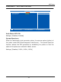
LOAD FAIL-SAFE DEFAULTS
Phoenix - AwardBIOS CMOS Setup Utility
Standard CMOS Features
Load Fail-Safe Defaults
Advanced BIOS Features
Load Optimized Defaults
Advanced Chipset Features
Set Supervisor Password
Integrated Peripherals
Set User Password
Save & Exit Setup
Power Management Setup
PnP / PCI Configurations
Exit Without
Saving
N
Load Fail-Safe Defaults (Y/N)?
Frequency / Voltage Control
Esc : Quit
F9 : Menu in BIOS
: Select Item
F10 : Save & Exit Setup
Load Fail-Safe Defaults
This option is for restoring all the default fail-safe BIOS settings.
These
values are set by the mainboard manufacturer to provide a stable system with
basic performance.
Entering “Y” loads the default fail-safe BIOS values.
52
BIOS Setup
LOAD OPTIMIZED DEFAULTS
Phoenix - AwardBIOS CMOS Setup Utility
Standard CMOS Features
Load Fail-Safe Defaults
Advanced BIOS Features
Load Optimized Defaults
Advanced Chipset Features
Set Supervisor Password
Integrated Peripherals
Set User Password
Save & Exit Setup
Power Management Setup
PnP / PCI Configurations
Exit Without
Saving
Load Optimized Defaults (Y/N)?
N
Frequency / Voltage Control
Esc : Quit
F9 : Menu in BIOS
: Select Item
F10 : Save & Exit Setup
Load Optimized Defaults
This option is for restoring all the default optimized BIOS settings.
The
default optimized values are set by the mainboard manufacturer to provide a
stable system with optimized performance.
Entering “Y” loads the default optimized BIOS values.
53
Chapter 3
SET SUPERVISOR / USER PASSWORD
Phoenix - AwardBIOS CMOS Setup Utility
Standard CMOS Features
Load Fail-Safe Defaults
Advanced BIOS Features
Load Optimized Defaults
Advanced Chipset Features
Set Supervisor Password
Integrated Peripherals
Set User Password
Security Chip Configuration
Power Management Setup
Save & Exit Setup
Enter Password:
Exit Without Saving
PnP / PCI Configurations
Frequency / Voltage Control
Esc : Quit
F9 : Menu in BIOS
: Select Item
F10 : Save & Exit Setup
Load Fail-Safe Defaults
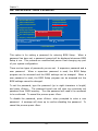
This option is for setting a password for entering BIOS Setup.
When a
password has been set, a password prompt will be displayed whenever BIOS
Setup is run. This prevents an unauthorized person from changing any part
of your system configuration.
There are two types of passwords you can set. A supervisor password and a
user password.
When a supervisor password is used, the BIOS Setup
program can be accessed and the BIOS settings can be changed. When a
user password is used, the BIOS Setup program can be accessed but the
BIOS settings cannot be changed.
To set the password, type the password (up to eight characters in length)
and press <Enter>. The password typed now will clear any previously set
password from CMOS memory. The new password will need to be reentered
to be confirmed. To cancel the process press <Esc>.
To disable the password, press <Enter> when prompted to enter a new
password. A message will show up to confirm disabling the password. To
cancel the process press <Esc>.
54
BIOS Setup
Additionally, when a password is enabled, the BIOS can be set to request the
password each time the system is booted. This would prevent unauthorized
use of the system. See “Security Option” in the “Advanced BIOS Features”
section for more details.
55
Chapter 3
SAVE & EXIT SETUP
Phoenix - AwardBIOS CMOS Setup Utility
Standard CMOS Features
Load Fail-Safe Defaults
Advanced BIOS Features
Load Optimized Defaults
Advanced Chipset Features
Set Supervisor Password
Integrated Peripherals
Set User Password
Power Management Setup
PnP / PCI Configurations
Save & Exit Setup
Exit Without
Saving
N
SAVE to CMOS & EXIT (Y/N)?
Frequency / Voltage Control
Esc : Quit
F9 : Menu in BIOS
: Select Item
F10 : Save & Exit Setup
Save Data to CMOS
Entering “Y” saves any changes made and exits the program.
Entering “N” will cancel the exit request.
56
BIOS Setup
EXIT WITHOUT SAVING
Phoenix - AwardBIOS CMOS Setup Utility
Standard CMOS Features
Load Fail-Safe Defaults
Advanced BIOS Features
Load Optimized Defaults
Advanced Chipset Features
Set Supervisor Password
Integrated Peripherals
Set User Password
Power Management Setup
PnP / PCI Configurations
Save & Exit Setup
Exit Without
Saving
N
Quit Without Saving (Y/N)?
Frequency / Voltage Control
Esc : Quit
F9 : Menu in BIOS
: Select Item
F10 : Save & Exit Setup
Abandon all Data
Entering “Y” discards any changes made and exits the program.
Entering “N” will cancel the exit request.
57
Chapter 3
This page is intentionally left blank.
58
CHAPTER 4
Driver Installation
This chapter gives you brief descriptions of each mainboard driver and
application. You must install the VIA chipset drivers first before
installing other drivers such as audio or VGA drivers. The applications
will only function correctly if the necessary drivers are already
installed.
59
Chapter 4
DRIVER UTILITIES
Getting Started
The mainboard includes a Driver Utilities CD that contains the driver utilities
and software for enhancing the performance of the mainboard. If the CD is
missing from the retail box, please contact the local dealer for the CD.
Note:
The driver utilities and software are updated from time to time. The latest
updated versions are available at http://www.viaembedded.com/
60
Driver Installation
Running the Driver Utilities CD
To start using the CD, insert the CD into the CD-ROM or DVD-ROM drive.
The CD should run automatically after closing the CD-ROM or DVD-ROM drive.
The driver utilities and software menu screen should then appear on the
screen. If the CD does not run automatically, click on the “Start” button and
select “Run…” Then type: "D:\Setup.exe".
Note:
D: might not be the drive letter of the CD-ROM/DVD-ROM in your system.
61
Chapter 4
CD CONTENT
VIA 4in1 Drivers: Contains VIA ATAPI Vendor Support
Driver (enables the performance enhancing bus mastering
functions on ATA-capable Hard Disk Drives and ensures IDE
device compatibility), AGP VxD Driver (provides service routines
to your VGA driver and interface directly to hardware, providing
fast graphical access), IRQ Routing Miniport Driver (sets the
system's PCI IRQ routing sequence) and VIA INF Driver
(enables the VIA Power Management function).
VIA Graphics Driver: Enhances the onboard VIA graphic
chip.
VIA Audio Driver: Enhances the onboard VIA audio chip.
VIA USB 2.0 Driver: Enhances VIA USB 2.0 ports.
VIA LAN Driver: Enhances the onboard VIA 10/100M LAN
chip.
VIA RAID Driver: Support for SATA RAID devices.
62