1
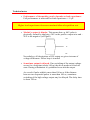
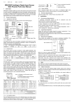
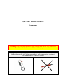
rev 1.05 / 2015 01 05
QBU-10kV Pockels cell driver
User manual
Warning! This equipment produces high voltages that can be very dangerous.
Please read user manual before starting operations.
Important note: please measure the output with symmetrical (differential)
high voltage probe only. Measurement made with inappropriate equipment
is a common cause of driver’s failure.
Overview
QBU-10kV Pockels cell driver produces high voltage pulses with high repetition
rate, fast risetime and falltime, adjustable voltage amplitude and pulse width. Two
control types are available: manual and automatic
Interfaces / signals / descriptions
INTERFACE (Molex 39-30-1060):
INTERFACE
8 7 6 5
4 3 2 1
PIN (color)
DESIGNATION
DESCRIPTION
While “0” or ”1” is applied to PIN1 high
voltage output is maintained
correspondingly at 0V or HV level
1 (transparent)
Pulse
2 (violet)
Temperature
Monitor
3 (red)
+15 V
Provides +15V DC output level;
maximal current capability is 100mA
4 (blue)
Enable
HV output is enabled / disabled by PIN4
(“1” – enable, “0” – disable)
5, 6 (black)
Interface Return
7 (yellow)
HV Monitor
Sequences of incoming pulses with period
less than approx. 200 ns will be ignored by
the driver
Provides internal temperature state (see also
temperature monitor section)
PIN5 and PIN6 are connected to the
driver’s ground circuit
The voltage at PIN7 is a monitor signal
proportional to the measured value of the
high voltage output
10kV corresponds to 10V at PIN7,
4kV corresponds to approx. 4V at PIN7
8 (green)
HV Program
Positive DC voltage applied to PIN8 sets up
high voltage value HV
10kV corresponds to 10V at PIN8,
4kV corresponds to approx. 4V at PIN8
“0” means logical 0 low level (0V), “1” means logical 1 high level (5V)
+24V (Molex 39-30-1040):
+24V
4 3
2 1
PIN (color)
DESIGNATION
DESCRIPTION
1, 2 (red)
+24V DC
INPUT positive 24V DC for turn on the
Pockels cell driver
3, 4 (black)
RETURN
Return from power supply producing
+24V DC
HV OUTPUT (Molex 39-30-1060):
PIN (color)
DESIGNATION
DESCRIPTION
1 (blue)
Negative
HV Negative
4 (red)
Positive
HV Positive
2, 3, 5-8
N/C
-
“ENABLE” JUMPER:
One can use “ENABLE” JUMPER instead of “ENABLE” signal of
INTERFACE. It isn’t recommended to use “ENABLE” JUMPER and
“ENABLE” signal at the same time.
“HV PROGRAM” JUMPER AND “HV PROGRAM” TRIMPOD:
One can use “HV PROGRAM” JUMPER instead of “HV PROGRAM”
signal of INTERFACE. If this jumper is set on, the output voltage is defined
with “HV PROGRAM” TRIMPOD state. It isn’t recommended to use
“HV PROGRAM” JUMPER and “HV PROGRAM” signal at the same time.
Safety
Warning! This equipment produces high voltages that can be very dangerous.
Don’t be careless around this equipment
Avoid casual contacts of personnel with output cables and with the load
Do not connect / disconnect cables while driver is turned on
Do not operate with disconnected load
Be very careful setting jumpers on and off and using HV Program trimpot;
accidental contact to the board may be fatal; from the same point of view it’s
recommended to control the driver not manually, but remotely via Interface
connector
• Be careful with driver’s neighborhood; do not store disordered items close to
any side of the driver
• Do not turn the driver on if it was already damaged with water, chemicals,
mechanical or electrical shock; do not self-repair the driver
•
•
•
•
Operations (Manual control)
1.
2.
3.
4.
5.
6.
Connect +24VDC power supply, pulse generator and Pockels cell
Set up “HV PROGRAM” JUMPER
Turn on +24VDC power supply
Set up “ENABLE” JUMPER
Use “HV PROGRAM” TRIMPOD to set up required output voltage
Send driving pulses from pulse generator to PIN1 of INTERFACE.
Set pulse width longer than 200 ns
7. To power down the driver, turn off +24VDC power supply or remove
“ENABLE” JUMPER
Operations (Automatic control)
1.
2.
3.
4.
5.
Connect +24V, INTERFACE and HV OUTPUT connectors to the board
Remove “HV PROGRAM” JUMPER, remove “ENABLE” JUMPER
DISABLE the high voltage output
Apply the correct nominal DC INPUT power to the module
Set up the required output voltage by applying a DC voltage to the
HV PROGRAM PIN8 of INTERFACE
6. ENABLE the high voltage output
7. Send driving pulses to PIN1 of INTERFACE.
Set pulse width longer than 200 ns
8. To power down the driver, remove DC INPUT power or DISABLE high
voltage output
Technical notes
• Performance of the module greatly depends on load capacitance.
Full performance is achievable at load capacitance < 11 pF.
Higher load capacitance decreases maximal allowed repetition rate
• Module’s output is bipolar. This means that e.g. 4kV pulse is
physically formed by applying +2kV to the positive output wire and –
2kV to the negative (see figure)
+2kV
0V
-2kV
Nevertheless, all descriptions of HV output are given in terms of
voltage differences. Please keep it in mind!
• Sometimes output is delayed. If no switching of the output voltage
occurs for a long time (about 100 us) the driver needs to refresh its
state. During refreshment it’s prohibited to switch the output.
As a result if pulse width is more than 100 us or if the distance
between two sequential pulses is more than 100 us, sometimes
switching of the high voltage output may be delayed. The delay time
is about 150 ns.
Specifications
ELECTRICAL SPECIFICATION
1
2
Input
Output
Working mode
HV higher level 1
HV lower level 1
Pulse width
Max. repetition rate
Risetime / falltime
Jitter
Delay time
Protections
Environment
Operation temperature
Storage temperature
Humidity
+24V DC; 0.5 A max
repetition of the input TTL signal
adjustable in 4 – 10 kV range
0 V, fixed
200 ns – DC
> 1 kHz at the full load (10 kV, 11 pF)
< 20 ns / <25 ns 2
~ 1,5 ns
~ 150 ns
from overheating (approx. 72 °C)
0...+40 °C
-20...+60 °C
90%, non-condensing
In terms of bipolar output (see also Technical notes section)
10-90% level, warranted at load capacitance 11 pF and below
MECHANICAL SPECIFICATION
Size (LxWxH) 132 x 105 x 50 mm
Weight < 0,2 kg