1
D-4 Nitrogen-Vacancy Centers in Diamond
From Physics 191r
contributors: M. Lukin, S. Zibrov, M. Goldman (2012)
N-V Centers in Diamond (Sept. 2012 pdf) File:Nvlab 4.pdf
Contents
1 Probing & control of single quantum systems in diamond
2 Summary
3 Learning Goals
4 Introduction
5 Structure of the NV center
5.1 Physical structure
5.2 Electronic structure
6 Experiment
7 Isolation of single NV centers: single photon source
8 Spin properties of the NV center
8.1 Optically induced spin polarization
8.2 Spin-dependent fluorescence
9 Single spin magnetic resonance: experiments
9.1 Continuous-wave experiments
9.2 Pulsed microwave experiments
9.2.1 Rabi oscillations
9.2.2 Ramsey fringes and spin echo
10 Photos
11 Apparatus
11.1 Confocal Microscope
11.1.1 Laser
11.1.2 Acousto-optic modulator: Crystal Technology 3080-125/controller 1080AF-DIFO1.0
11.1.3 Green fiber
11.1.4 Neutral density filters
11.1.5 Home Made Power Meter
11.1.6 Galvo-controlled mirrors: Thorlabs GVS012
11.1.7 Scanning microscope: principle of operation
11.1.8 Objective: Nikon MRH01902 CFI Plan Fluor 100x Oil Immersion
11.1.9 Sample
11.1.10 Translation stage: Newport 562-XYZ
11.1.11 Dichroic beamsplitter: Semrock LM01-552-25
11.1.12 Red detection
11.1.13 Single Photon Counting Modules: Perkin Elmer SPCM-AQR-14-FC
11.2 National Instruments PCIe-6323 X Series Multifunction ePCI card
11.3 LabVIEW program NV_191.vi
11.4 PicoQuant TimeHarp 200 PCI board for Time-Correlated Single Photon Counting
11.5 Microwave Source and Amplifier
11.5.1 INPUTS
11.5.2 INDICATORS
11.6 Electronics block diagram
11.7 SpinCore Technologies PulseBlaster ESR-PRO-400 PCI Pulse Generator Board
11.8 Pulse Experiments
11.8.1 Rabi
11.8.2 Ramsey
11.8.3 Hahn Echo
11.8.4 Readout
12 References
13 Introductory reading
14 Bench notes
15 Appendix: microwave source calibration
Probing & control of single quantum systems in diamond
Summary
This experiment explores control over individual quantum objects such as single photons and single electronic
spins. It utilizes a confocal microscope to isolate and manipulate individual atom-like impurity in a diamond
crystal. Optical excitation of this isolated impurity is used to study a very unusual light source in which single
photons are emitted one at a time. Optical and microwave radiation is then used to control and manipulate the
electronic spin state associated with the single impurity. Experimental techniques and methods introduced in
this experiment form the basis for an exciting modern research direction, involving the applications of
individual atoms and atom-like systems for quantum information processing, communication and metrology.
Learning Goals
Use a confocal microscope to observe nitrogen-vacancy centers in diamond.
Measure the correlation function for light emitted by a single n-v center to observe anti-bunching.
Measure Zeeman splitting of the ground and excited states of an n-v center.
Observe Rabi oscillations of a single electron.
Introduction
Control of quantum systems is an important topic in contemporary physics research, with many types of
experiments aimed at applications ranging from metrology and interferometry to quantum communication and
quantum computation.[1] The key to realization of these concepts and their potential applications is to gain a
control over individual quantum systems, such as single photons, atoms, electrons and nuclei. This control
should include the ability to prepare and measure such individual degrees of freedom of such systems as well as
to manipulate their various degrees of freedom. For example, secure quantum cryptography can be realized by
encoding bits of information into polarization degrees of freedom of individual photons. At the same time, spin
degrees of freedom associated with individual electrons can be used as basic building blocks of quantum
information processors (quantum bits), or, as an atomic-scale sensors of local fields. [2]
A variety of physical systems lend themselves to such investigations, and each offers a different set of
opportunities and challenges. This experiment explores control over individual quantum systems using the socalled Nitrogen-Vacancy impurity in diamond. Such nitrogen-vacancy (NV) centers have been studied for
several decades using a variety of spectroscopic techniques. Recently, there has been renewed interest in the NV
center as a physical system for quantum information science in the solid state. The NV center is an attractive
quantum bit (qubit) candidate because it behaves like an atom trapped in the diamond lattice: it has strong
optical transitions, and an electron spin degree of freedom. In what follows we consider the basic structure of
the NV center and describe experimental techniques used to probe its spin and optical properties.
Structure of the NV center
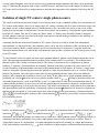
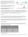
Physical structure
The NV center is formed by a missing carbon atom adjacent
to a substitutional nitrogen impurity in the face-centered
cubic (fcc) diamond lattice (see Fig. 1A). The physical
structure of this defect -- and the symmetries associated
with it -- determine the nature of its electronic states and the
dipole-allowed transitions between them (see Fig. 2).
The symmetry properties of the NV center provide insight
Figure 1. (A) The nitrogen-vacancy center in
into the nature of its electronic states. Unlike atoms in free
diamond. (B) The symmetry operations for the C3v
space, whose electronic states are governed by their
group include rotations by 2!n / 3 around the
rotational invariance, the NV center exhibits C3v symmetry,
vertical symmetry axis and reflections in the three
as illustrated in Fig. 1B. Electronic states are thus
planes containing the vertical symmetry axis and
one of the nearest-neighbor carbon sites.
characterized by how they transform under C3v operations.
A1 energy levels consist of a single state which transforms
into itself, with no sign change, under all symmetry operations. A2 levels are also non-degenerate, but the state
picks up a negative sign under reflections. Finally, E levels consist of a pair of states, which transform into each
other the way that the vectors and transform into each other under C3v symmetry operations. For more
details on C3v symmetry and group theory, see Appendix of L. Childress' thesis. [3]
Electronic structure
Although a number of efforts have been made to elucidate the electronic structure of the NV center from first
principles, [4][5][6] it remains a topic of current research. Experimentally, it has been established that the NV
center exists in two charge states, NV0 and NV " , with the neutral state exhibiting a zero-phonon line (ZPL) at
575nm and the singly charged state at 637nm (1.945 eV).[7] In this work we consider exclusively NV " , which
is dominant in natural diamond, and will refer to it simply as the NV center. The electron configuration for the
neutron NV0 center is a follows. The five valence electrons of the nitrogen atom form covalent bonds with the
three nearest neighbor carbon atoms while the remaining
two form a lone pair that points in the direction of the
neighboring carbon vacancy. The three unpaired valence
electrons of the carbon atoms adjacent to the carbon
vacancy occupy molecular orbitals. Two of these electrons
occupy the lowest energy orbital with antiparallel spins
while the third spin is unpaired. The NV0 center is
paramagnetic with spin S=1/2. The charged NV " center is
formed by addition of one more electron which combines
with the unpaired electron of NV0 to form a spin S=1.
The NV center has C3v symmetry, with the ZPL emission
band associated with an A to E dipole transition. Holeburning,[8] electron spin resonance (ESR), [9][10] optically
detected magnetic resonance (ODMR),[11] and Raman
heterodyne[12] experiments have established that the ground
electronic state is a spin triplet 3A2. This triplet is itself split
by spin-spin interactions, yielding one state with
with A1 character and two
states with E
character [13] which are 2.87 GHz higher in energy.
Together with the 637nm ZPL, the 2.87 GHz zero-field
ground-state splitting allows identification of a defect in
diamond as an NV center.
Figure 2. (a) The electronic structure of the NV
center. The orbital states are indicated on the left
hand side, and the spin-spin splitting of the ground
state is indicated on the right hand side. After
accounting for all spin-orbit, spin-spin, and strain
perturbations, the structure of the six electronic
excited states remains a topic of current research.
Vibronic sideband transitions used in excitation are
indicated by the yellow continuum. (b) The level
diagram corresponding to ground and excited
electronic states (manifolds), including the effect of
lattice vibrations. The phonon relaxation within each
of the manifolds is very fast, and the individual
vibrational states can not be resolved. When the NV
center is excited with green light (532 nm), it
rapidly relaxes to the lowest vibrational state within
the excited electronic manifold via phonon
emission. The spontaneous photon decay of the
electronic excited state (measured in our
experiments) can occur directly into the ground state
(Zero Phonon Line, ZPL, 637 nm) or into excited
vibrational states (Phonon Side Band, PSB), from
which it relaxes rapidly into the ground state via
phonon emission.
In addition to the discrete electronic excited states which
contribute to the ZPL, there are a continuum of vibronic
excited states which appear at higher frequencies in
absorption and lower frequencies in emission. When the
vibronic states are excited using for example a 532 nm laser, phonon relaxation brings the NV center quickly
into one of the electronic excited states. The NV center then fluoresces either via emission of 637 nm ZPL
photon, or via a process in which photon emission is accompanied by a phonon (the so-called phonon
sideband). The fluorescence in phonon sideband (PSB) is lower in frequency than that of ZPL, and extends
from 650-800 nm. In practice, fluorescence into the ZPL accounts for only a few percent of the emitted light,[14]
thus in the experiment broadband PSB fluorescence is collected.
Experiment
Many of the early experiments on NV centers looked at ensemble properties, averaging over orientation, strain,
and other inhomogeneities. Recently, confocal microscopy techniques have enabled examination of single NV
centers, [15] permitting a variety of new experiments studying photon correlation statistics,[16][17] single optical
transitions,[18] coupling to nearby spins,[19] and other effects difficult or impossible to observe in ensemble
studies.
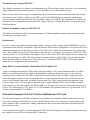
To study NV centers in diamond, we use a scanning
confocal microscope incorporating magnetic field control
and microwave coupling. The confocal microscope[20] uses
point illumination and detection along the identical path, in
order to increase the signal to noise ratio.The essential
features of the apparatus are shown in Fig. 3.
The sample we use is a type IIa diamond specially selected
for low nitrogen content (
). This low nitrogen
content is critical for observing coherent processes of the
NV spin degree of freedom, because the electron spin
associated with nitrogen donors interacts strongly with the
NV center spin.[21] In the experiment, we study the NV
centers that occur naturally in bulk diamond.
Our measurements rely on optically exciting a single NV
within the sample, and detecting its fluorescence. Excitation
into the vibronic sideband of the NV center is performed
using a 532 nm doubled-YAG laser. The excitation beam
passes through a fast Acousto-Optic Modulator (AOM) (rise
time
), allowing pulsed excitation with widths of
less than 100 ns, and are focused onto the sample with an oil
immersion lens (Nikon Plan Fluor 100x NA 1.30).
Figure 3. Diagram of the experimental setup.
Figure 4. Diamond plate is mounted on a silicon
wafer. It is subjected to a microwave field via a
copper wire.
To control the position of the focal spot on the sample we
employ a closed-loop X-Y galvanometer combined with a
piezo objective mount for focus adjustment. The mirrors forming the galvanometer are imaged onto the back of
the objective, so that they vary the position of the focal spot without affecting the transmitted laser power.
Scanning the galvanometer mirrors thus allows us to scan the focal spot over a plane in the sample, with a
maximum scan range of about 100 x 100 #m2.
Fluorescence from an NV center is collected by the same optical train, so that the detection spot is scanned
along with the excitation spot. The fluorescence into the phonon sideband (650-800nm) passes through the
dichroic mirrors (which combine the excitation lasers with the optical train), and a 600 nm long-pass filter
before being coupled into a single-mode fiber. In many confocal setups, the point source emission is imaged
onto a pinhole for background rejection; in our setup, the single-mode fiber replaces the pinhole. Ideally, this
constitutes mode-matching between the mode collected by the objective from the NV center point source and
the mode of the fiber. The fiber is itself acts as a beamsplitter, whose two outputs are connected to fiber-coupled
single photon counting modules (SPCMs, Perkin-Elmer). Overall, the collection efficiency for fluorescence
from the sample is just under
.
To apply strong microwaves to the NV center, the sample is mounted on a circuit board with a microwave
stripline leading to and away from it. A 20 #m copper wire placed over the sample is soldered to the striplines.
By considering NV centers close to the wire, we can achieve large amplitudes for the oscillating magnetic field
with modest microwave power through the wire.
A static applied magnetic field can be varied using a permanent magnet mounted on a three axis translational
stage. To measure the magnetic field, a three-axis Hall sensor is mounted close to the sample. In addition, the
NV center itself can be used as a magnetometer to measure the component of the magnetic field along the NV
axis.
Isolation of single NV centers: single photon source
The small excitation and detection volume of our confocal microscope, combined with the low concentration of
NV centers in the sample, allows us to image single NV centers. Scanning the focal spot of the microscope over
the sample reveals scattered bright spots of similar intensity. We can position the focus on top of one of the
bright spots and examine its fluorescence. Several observations can be made to verify that the signal originates
from the NV centers. First, the NV centers are photo-stable, i.e. fluorescence should not blink or disappear.
Second, photon-count rate associated with single atom emission should undergo saturation as the intensity of
the excitation laser is increased.
Assuming that the the excited state lifetime of NV centers is known or could be found from independent
measurements (as discussed below), the saturation curve can be used for calibration of the excitation rate for a
given laser intensity. Make a simple model to predict a fractional form of saturation. Using this model and
saturation measurements, you can find the correspondence between the excitation rate and a laser power for any
given NV center.
To verify that the observed signals are from single quantum emitters, photon correlation measurements can be
used. One important quantum mechanical property of the radiation field is its statistics. The radiation from
thermal sources (like a lamp) or coherent sources (like laser) is characterized by a distribution of photon
numbers. A sequence of measurements on nominally identical weak pulses produced by such sources will
reveal fluctuations in photon number associated with quantum nature of such pulses. In contrast, a single atom
emitter is incapable of producing more than one photon at a time and can therefore serve as a source of single
photons. In principle, one could observe this effect by histogramming the time interval between different
photons, and examining the distribution close to zero delay. If the source was a single quantum emitter, the
probability for a delay between successive photons should vanish as
. Owing to dead-time effects for
avalanche photodetectors, such as the SPCMs we use, it is impossible to make such a measurement directly. To
circumvent this problem it is necessary to divide the emitted photons between two detectors, and measure the
time interval between a click in one detector and a click in the second detector. In the limit of low count rates,
this measurement yields the probability of measuring a photon at time conditional on detection of a photon at
time , which corresponds to a two-time expectation value for the fluorescence intensity correlation function,
. Normalizing this quantity to the overall intensity
yields the second order correlation function
for a stationary process
Ideally, we should observe
for emission from a single quantum emitter, whereas classical sources
must have
.[22] Since a two-photon state has
, observation of
is
sufficient to show that the photons are emitted one at a time by a single quantum system. The physical origin of
vanishing coincidence probability for a perfect single photon source can be understood as follows. When a
single photon arrives at a beamsplitter, it is either transmitted or reflected, resulting in a single photodetector
click, and vanishing coincidence at
. Such a behavior of photon-photon correlation function represents
direct evidence for quantum mechanical nature of light field. This is one of the most fundamental phenomena in
quantum optics.[23]
Development of single photon sources is an active field of modern research. The NV center has received
considerable attention as a robust, room temperature source of single photons, [24][25][26][27] and it is currently
being used for quantum key distribution and other applications.
Photon correlation measurements and, specifically, the width of the anti-correlation feature can be used to
quantify population dynamics of the NV center. Intuitively, the counter board measures the probability of
photon emission (proportional to population of excited state, , as a function of time, triggered by an initial
photon emission that prepares the NV center in its ground state. Using the rate equation model one finds that
(show this!), where is optical excitation rate, proportional
to light intensity and is total decay rate from the excited state.[28][29] In your experiment, you can measure
photon correlations for different pump powers and try to use the power dependence to determine the excited
state lifetime.
Spin properties of the NV center
While discussing the electronic structure of the NV center, we have already touched upon the existence of an
spin degree of freedom in the ground and excited states. In this section, we will consider in greater
detail the interplay between optical transitions and the spin degree of freedom.
Optically induced spin polarization
Early experiments established that the NV center spin shows a finite polarization under optical illumination
with green light (see Fig. 2). Over the years, it has been determined that optical excitation causes the ground
state to become occupied with high probability, and recent measurements indicates that nearly full
polarization may occur.[30] Nevertheless, the precise mechanism for optically induced spin polarization is still a
topic of active research.[31][32]
Spin polarization originates due to existence of a singlet electronic state whose energy level lies between the
ground and excited state triplets (see Fig. 2). Transitions into this singlet state occur primarily from
states, whereas decay from the singlet leads primarily to the
ground state.[33] If the remaining optical
transitions are spin-preserving, this mechanism should fully polarize the NV center into the
ground
state.
Spin-dependent fluorescence
Most current research on the NV center in diamond relies on optical detection of its ground state spin.
Experimentally, an NV center prepared in the
state fluoresces more strongly than an NV center
prepared in the
state.[34] Optically detected magnetic resonance in the NV center was observed first
at low temperature in ensemble studies.[35][36] At room temperature, this allows for efficient detection of the
average spin population; using resonant excitation at low temperature, the effect is more pronounced, and
single-shot readout is possible.
Specifically, at room temperature, the same mechanism which leads to optical spin polarization provides the
means to optically detect the spin state. Non-resonant green excitation (at e.g. 532 nm) excites transitions from
both the
and
ground state levels. However, because the intersystem crossing occurs
primarily from the
excited state, population in
ground state undergoes fewer
fluorescence cycles before shelving in the singlet state for around 300 ns. The
states thus fluoresce
less than the
. [37][38][39]
state, with a difference of
Single spin magnetic resonance: experiments
The electron spin of an NV center can be polarized and measured using optical excitation, as discussed above.
By tuning an applied microwave field in resonance with its transitions, the spin can also be readily manipulated.
Although it is difficult to address a single spin with microwaves, one can prepare and observe a single spin by
confining the optical excitation volume to a single NV center. These ingredients provide a straightforward
means to prepare, manipulate, and measure a single electronic spin in the solid state at room temperature.[40]
The experiments involving the NV electron spin can be roughly divided into continuous-wave (CW) and pulsed
experiments. In both cases, we isolate a single spin using confocal microscopy and apply microwaves to it using
a 20 #m copper wire drawn over the surface of the sample (Fig. 4).
Continuous-wave experiments
For continuous-wave (CW) measurements, microwave and optical excitation are applied at constant power to
the NV center, and the fluorescence intensity into the phonon sideband is measured as a function of microwave
frequency. The continuous 532 nm excitation polarizes the electron spin into the brighter
state; when
the microwave frequency is resonant with one of the spin transitions
, the population
is redistributed between the two levels, and the fluorescence level decreases. In the absence of an applied
magnetic field, the electron spin resonance (ESR) signal occurs at 2.87 GHz, while in a finite magnetic field the
two transitions are shifted apart by
2.8 MHz/Gauss.
In this experiment, you will observe and explore single spin ESR signal. Explore experimentally and explain
how does this signal depend on applied microwave and optical power. Make a model for power dependance and
check its consistency with excitation rate measurements. Explore how the signal changes with applied magnetic
field.
Once the signal is optimized, close examination of a single
transition may reveal
hyperfine structure associated with the nitrogen forming the NV center. Some NV centers have a structure that
makes the hyperfine splitting more obvious. The
14N
nuclear spin has a hyperfine structure which is
governed by the Hamiltonian[41]
,
where
splits the
is the nitrogen nuclear spin and
states off from the
is the NV center electron spin. A strong quadrupole interaction
state by
orientation of the nitrogen nuclear spin for magnetic fields
MHz,[42] effectively freezing the
Tesla. In addition, the 14N nuclear spin
interacts with the electron spin
split from the
, so that in the electron spin excited state
state by
and
, the
states are
. Since the electron spin resonance transitions
cannot change the nuclear spin state, the three allowed transitions are separated by
MHz. To
resolve hyperfine structure, you will need to turn down the optical and microwave power such that the resulting
linewidths are below
. For laser power of a few milliWatts, a factor of 100 attenuation is typical;
microwave power has to be reduced in tandem.
These CW measurements served primarily as a means to calibrate the frequency of microwave excitation
appropriate for pulsed experiments. However, the 14N hyperfine structure illustrates that CW measurements can
also be useful for determining interaction strengths between the NV electron spin and other nearby spins.
Pulsed microwave experiments
Continuous-wave spectroscopy provides a means to measure the energy levels of the NV spin system. To
observe the spin dynamics, we must move to the time domain, and apply pulses of resonant microwaves. The
excitation sequence for pulsed microwave experiments is illustrated in Fig. 5A. All experiments begin with
electron spin polarization and end with electron spin measurement, both of which are accomplished using 532
nm excitation. In between, different microwave pulse sequences can be applied to manipulate the electron spin.
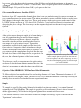
Rabi oscillations
In a small applied magnetic field, the
to
spin transition of the NV center constitutes an
effective two-level system. Driving this transition with resonant microwave excitation will thus induce
population oscillations between the ground
and excited
states; these are known as Rabi
oscillations.[43] To observe Rabi nutations, we drive the transition with a resonant microwave pulse of varying
duration and measure the population remaining in
. Fig.5B shows a typical Rabi signal.
For resonant microwave excitation, Rabi oscillations correspond to complete state transfer between
and
. This allows us to calibrate our measurement tool in terms of the population in the
state. As shown in Fig. 5B, we can identify the minimum in fluorescence with
and the maximum with
. For weak or off-resonant microwave fields one employs a more careful analysis, which fits the data to a
multi-level model including all of the hyperfine structure associated with the 14N nuclear spin and any other
nearby spins. In either case, we can present data from more complicated pulsed experiments in units of
population obtained from fits to Rabi nutations observed under the same conditions.
The frequency of the Rabi nutations depends on the
microwave power IMW as
. For a given
microwave power, we observe Rabi nutations to calibrate
the pulse length required to flip the spin from
to
; this is known as a pulse, because it corresponds
to half of the Rabi period. Shorter and longer pulses create
superpositions of the spin eigenstates; in particular, a
microwave pulse (i.e. of duration $ = % / &) sends the
state
into the superposition
. This corresponds to rotating the
Figure 5. Pulsed electron spin resonance. Pulse
sequence for Rabi oscillation (a) and Ramsey
effective spin-1/2 system
by about an axis in
sequence (b) experiments
the
plane. The relative phase of the two components
(or, equivalently, the orientation of the axis in the
plane) is set by the phase of the microwave excitation. For a single pulse, this phase does not matter (it could
equally well be incorporated into a redefinition of
), but composite pulse sequences often make use of shifts
in the microwave phase. As an example, a pulse A of duration
followed by a
degree phase shifted pulse
B of duration
would correspond to rotating the spin by
around the axis followed by a rotation by
around the axis.
Ramsey fringes and spin echo
Rabi nutations correspond to driven spin dynamics. We can also observe the free (undriven) spin dynamics by
generating a superposition of the spin eigenstates
and
, letting it evolve freely, and then
converting the phase between the two eigenstates into a measurable population difference. This is accomplished
using a Ramsey technique,[44] which consists of the microwave pulse sequence
as illustrated
in the inset to Fig. 5C. For a simple two-level system, the Ramsey sequence leads to population oscillations
with a frequency equal to the microwave detuning . Because of the 14N hyperfine structure, we observe a more
complex signal from three independent two-level systems. These three signals beat together, producing the
complicated pattern shown in Fig. 5C. The data can be modeled with three superposed cosines, corresponding
to the three hyperfine transitions.
The fit to the Ramsey data should also include an overall envelope such as Gaussian envelope
,
which decays on a timescale
known as the electron spin dephasing time. The dephasing time is the timescale
on which the two spin states
and
accumulate random phase shifts relative to one another.
For the NV center, these random phase shifts arise primarily from the effective magnetic field created by a
complicated but slowly-varying nuclear spin environment. These frequency shifts can be eliminated by using a
spin-echo (or Hahn echo) technique.[45] It can be used to extend the coherence time and to gain addition
insights into spin dynamics.
Spin echo consists of the sequence
(see Fig. 5A), where represents a
microwave pulse of sufficient duration to flip the electron spin from
to
, and
are
durations of free precession intervals. As with the Ramsey sequence, the Hahn sequence begins by preparing a
superposition of electron spin states
using a
microwave pulse. This superposition
precesses freely for a time , so that, for example, the
component picks up a phase shift '$ relative to the
component, yielding
. The ! pulse in the middle of the spin-echo sequence flips
the spin, resulting in the state
since the first free precession interval, the
. Assuming that the environment has not changed
component will pick up the phase
precession interval, leaving the system in the state
are precisely equal,
population back into
with a delay
.
during the second free
. When the two wait times
, the random phase shift factors out, so the final
pulse puts all of the
. When the wait times are unequal, the Hahn sequence behaves like a Ramsey sequence
Spin echo is widely used in bulk electron spin resonance (ESR) experiments to study interactions and determine
the structure of complex molecules.[46] Likewise, spin-echo spectroscopy provides a useful tool for
understanding the complex mesoscopic environment of a single NV center: by observing the spin-echo signal
peak (
), we can decouple spin dynamics from low-frequency environment, extend its coherent evolution
and can indirectly glean details about the environment itself.
Finally, spin echo and other related decoupling techniques constitute an important tool for extending coherence
times of spin qubits. Applications of such techniques ranging from quantum computation to nanoscale
magnetometry are at the forefront of the modern research.
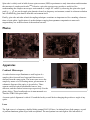
Photos
Confocal microscope.
Laser.
Apparatus
Confocal Microscope
A confocal microscope illuminates a small region of a
sample with a focussed laser beam and fluorescence is
detected from the same region. The beam scans across the
sample by means of a 2D rotating mirror galvanometer. A
schematic diagram of the optics is given below. Three
separate enclosed optical breadboards house a laser,
detectors, and the confocal microscope respectively. See the
photos below. These breadboards are in turn mounted on a
Thorlabs PTR11104 optical table.
Detectors.
Accurate optical alignment is critical. Consult the faculty or staff before changing the position or angle of any
optics.
Laser
The light source is a frequency-doubled diode-pumped Nd-YAG laser. An infrared laser diode pumps a crystal
of yttrium aluminum garnet doped with neodymium. The neodymium ions emit light at 1064 nm which is
frequency-doubled in a crystal of potassium dihydrogen
phosphate (KDP). The nominal power of the laser is 200
mW. If you open the laser box when the laser is on, use the
Thorlabs LG-10 laser safety glasses to block both the 532
nm and 1064 nm light.
The laser power supply is housed in a small black box with
a key switch. As a safety precaution return the key to the
blue cabinet at the end of each lab session.
Acousto-optic modulator: Crystal Technology 3080125/controller 1080AF-DIFO-1.0
Confocal microscope block diagram.
An acousto-optic modulator mounted in the laser box switches the light output off and on. The optical element
of an AOM is a crystal of tellurium dioxide. A piezo-electric transducer mounted on the crystal produces an
acoustic wave in the crystal in response to an rf voltage across it. The light diffracts from the acoustic wave in a
process similar to Bragg reflection. Two output beams are generated: a zero-order beam which is simply
transmitted through the TeO$_2$, and a diffracted beam which is coupled to a fiber.
Green fiber
A single mode fiber, Thorlabs P1-630A-FC-2, transmits light from the laser box to the confocal microscope
box. As currently configured (Spring 2012) the output of the fiber is approximately 3 mW. The "mode field
diameter" of the fiber is 4.3 microns. The fiber does not transmit 1064 nm light efficiently.
A Thorlabs F230FC-B fiber collimator couples the free space laser beam into the fiber in the green laser box. A
Thorlabs CFC-8X-A adjustable collimator is used at the other end of the fiber in the confocal microscope box.
The focal length of this collimator is 7.5 mm and the output beam waist diameter is 1.2 mm.
Neutral density filters
Immediately downstream of the fiber coupler is a filter wheel housing neutral density filters. Use these to
attenuate the laser power. Nominal values of the filters are given in the table. For additional attenuation use the
ND 1.0 filter mounted on a one-inch post.
number on filter wheel attenuation (log scale) transmission (linear scale)
1
2
0.0
0.1
1.00
0.79
3
0.2
0.63
4
5
0.3
0.5
0.50
0.32
6
1.0
0.10
Home Made Power Meter
A photodiode mounted on a moveable post is used to measure the laser power leaving the fiber. To measure the
laser power, place the photodiode downstream of the ND filters and switch the multimeter to dc current
. The calibration is: 2.76 mW / 275 microAmps. This is a typical power used to excite the NVs in the
diamond sample. %If you find less than 2 mW, cycle power to the laser.
Galvo-controlled mirrors: Thorlabs GVS012
In order to locate NV centers in the diamond plate, there is an xyz translation stage for course movement, and
galvo controlled mirrors for fine movement. The mirrors, mounted on motor-controlled shafts are used to make
small changes in the angle of the laser beam. These are dc motors which receive power under control of the
LabVIEW software at the rate of 1.25 degree/Volt. The Galvo Controls tab has buttons for increasing and
decreasing the galvo voltages. The Arrow keys on the computer keyboard are shortcuts for up/down and
right/left.
Scanning microscope: principle of operation
As the galvo mirrors change the angle of the beam during a
scan, we require that the green and red beams remain
colinear. If this were not the case, detection would be
impossible since the red beam would miss the fiber for
some range of the galvo mirrors' travel. To meet this
requirement, an optical trick is employed. The lens in the
figure refers to a composite of three actual lenses: the pair
of lenses downstream of the mirrors plus the objective. The
galvo mirrors and the sample plane are placed into the front
and back focal planes of the composite lens, respectively. In
this case, the collimated portions of the beams remain
colinear.
This telescope as well as one upstream of the galvo mirrors
are chosen so that the beam diameter matches the size of the
objective's rear aperture to make the sharpest possible focus.
Principle of confocal microscope. The Galvo mirror
and the sample plane are placed into the front and
back focal planes of the lens, respectively. In such a
case, the excitation path (green) and collection path
(red) can be identical.
Objective: Nikon MRH01902 CFI Plan Fluor 100x Oil Immersion
The Nikon objective has magnification 100x and working distance of 0.2 mm. The numerical aperture is 1.30
and the effective focal length is 2 mm. The field of view is 0.18 mm. The immersion oil has high viscosity and
normally does not need to be refreshed between experimental runs.
Sample
The sample is a type IIa (high purity) diamond selected for low nitrogen content. It is a natural diamond
originating in the Ural Mountains. The sample is epoxied to a silicon substrate. Silicon is chosen because it
absorbs approximately 70\% of the incident green light, and does not emit red fluorescence.
Under normal operation, it is not advisable to remove the sample for viewing. A photo is included in the
"Experiment" section above.
Translation stage: Newport 562-XYZ
The sample is mounted on a stainless steel translation stage. The translation stage is used for coarse positioning
during alignment. Under normal operation, it is not advisable to move the translation stage.
However fine control of focussing is accomplished with a piezoelectric transducer mounted under the vertical
micrometer screw. Voltage is applied to the PZT by a Thorlabs MDT693A piezo controller which in turn
receives an input control signal from the NI 6323 under control of LabVIEW. The \emph{Galvo Controls} tab
has buttons for increasing and decreasing the PZT voltage. The Page Up/Page Down keys are shortcuts for the
Shallower/Deeper.
Dichroic beamsplitter: Semrock LM01-552-25
The dichroic beamsplitter reflects green and transmits red. The beamsplitter separates the red detection beam
from the green excitation beam.
Red detection
In order to reject green light scattered from the sample, a long pass filter, Omega Optical 3RD600LP is placed
downstream of the dichroic beamsplitter. The transmission of the dichroic beamsplitter is one percent at 532 nm
whereas the transmission of the long-pass filter is only 10$^{-6}$ whereas the red transmission is greater than
80\%. The red light is focused by a second microscope objective, an Olympus 20X objective with NA 0.4. The
working distance is 1.2 mm and the focal length is 9 mm. A New Focus 9091 fiber coupler has fine controls for
the position and angle of a fiber. The fiber connector (Summer 2012) is slightly flaky. You may find the fiber
tied down with cable ties for this reason. This fiber leads to a Thorlabs FC632-50B-FC 50/50 beam splitter
which delivers red photons to the two detectors.
Single Photon Counting Modules: Perkin Elmer SPCM-AQR-14-FC
A pair of avalanche photodiodes (APDs) detect red light emitted by NVs in the diamond sample. An APD is
similar to an ordinary photodiode in that an incident photon strikes the depletion region of a p-n junction,
creating an electron-hole pair. The APD is different from a photodiode in the sense that a large reverse bias
across the depletion region creates an avalanche effect. A single electron liberates many secondary electrons,
each of which liberate many more secondary electrons and so on. Thus a single photon can generate a large
electrical signal. This is the same process that takes place in photomultiplier tubes, but all within a compact
solid state device. The dark count for the SPCM-AQR-14 is less than 100 counts/sec. Dead time after an event
is 50 ns. The APD output is a TTL pulse of 2.5 Volts minimum. The quantum efficiency is greater than 50% at
650 nm and greater than 35% at 830 nm.
National Instruments PCIe-6323 X Series Multifunction ePCI card
The National Instruments 6323 Data Acquisition card interfaces the computer with the confocal microscope.
Four analog outputs control both galvo motors, the PZT and the microwave attenuator. Counter/timers count
pulses from the APDs, synchronize counting with the microwave sweep and count pulses from the SpinCore
pulse generator card.
A rack-mounted breakout box, National Instruments BNC-2090A incorporates a rear-panel connector matching
the connectors on the 6323 to front-panel BNC connectors.
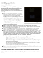
LabVIEW program NV_191.vi
(courtesy of Mike Goldman)
A LabVIEW program written by the Lukin group controls
the experiment and acquires data. Referring to the figure,
zones A through G are a collection of controls and
indicators. Data files can be saved using the controls in the
lower right.
Zone A is a map showing the intensity of red light
emitted by the sample. Scanning an appropriate area
is important since you may not see NVs if the
resolution is too low. Typical scan range is 0.2 V in X
and Y which corresponds to about 8 microns. As of
summer 2012, bright NVs can be seen in the range X
= [-0.1 V, +0.1 V], Y = [-0.4 V, -0.2 V]. This is for
micrometer settings X = 6.318 mm, Y = 7.555 mm
and Z = 6.023 mm. You can look anywhere in the
Front panel of NV LabVIEW program.
sample for NVs. To expedite your experiment,
consider using established parameters.
Zone B is a data window which varies from tab to tab. The "Counter Readout" tab is shown.
Zone C selects the active set of controls. The box below Zone C shows controls for Galvo Positioning',
PicoHarp, Microwave, Pulse Experiment, etc.
The box above Zone D contains controls for the Galvo Scan. The buttons below are start and stop
controls for Galvo Scan, Counter, NV lock, Microwave scan, Picoharp, and Pulse Experiments.
Zone E is the Optimize button -- important enough to have its own zone. The stability of the NV count
rate is usually good enough to make measurements for several minutes, but there is a tendency to drift.
Small changes in position caused by temperature fluctuation and other factors cause the signal to change
over time. "Optimize" is a routine which scans a small range of X and Y, looking for maximum signal.
Optimize before starting each data run. "NV lock" is automatic "Optimizing."
Zone F is a set of tabs:
Counter Readout is a graph of total counts (sum of two APDs) as a function of time.
NV Tracking Fits shows the fits computed by the "Optimize" routine.
NV Tracking History gives several ways of monitoring the position of an NV.
MW Scan Result is a graph of count rate synchronized with microwave sweep. Many sweeps are
averaged and the result displayed.
MW Scan History is a color representation of every microwave sweep in the series of averages.
Pulse Experiment controls pulsed ESR experiments.
PicoHarp displays the result of g2 correlation measurements.
Zone G activates the acousto-optic modulator, coupling the green laser light into the fiber, which in turn
illuminates the confocal microscope.
PicoQuant TimeHarp 200 PCI board for Time-Correlated Single Photon Counting
As discussed above in section 4, we wish to use the TimeHarp 200 to measure the second-order correlation
function,
for the photons emitted by an NV center.
The TimeHarp card measures and digitizes the time interval between two photon events. Two APDs each
receive approximately 50% of the NV photons and provide input pulses for the TimeHarp inputs SYNC and
START. The SYNC input requires a fast negative pulse to trigger a measurement. A positive pulse in the range
of 50 - 1500 mV at the START input stops the measurement. After a measurement, the time interval is added to
a histogram of up to 4096 bins. The TimeHarp card has an incredibly small time resolution of 40 ps. However
the dead time associated with each event is 350 ns.
Given the limitation of dead time, it is only possible to measure
when the count rate is low compared to
the histogram bin duration. (Is this approximation valid for typical experimental parameters?) Suppose that the
probability of detecting a photon in any particular time bin after a SYNC pulse is small. In this case most bins
will have zero counts and one particular bin, will receive one count and stop the measurement. The SYNC
pulse corresponds to
and
for most time intervals.
. Thus
apart
from the normalizing factor
. Repeating the measurement many times is necessary to build up a
histogram with adequate statistics. The maximum number of TimeHarp histogram bins is 4096.
We wish to observe
on a time scale smaller than the dead time of both the APDs and the TimeHarp.
To circumvent the APD dead time, we split the signal into two APDs. To circumvent the TimeHarp dead time, a
length of coaxial cable is inserted into the SYNC channel, moving the feature of interest to a time much longer
than the dead time. Since the APDs are nominally identical, in principle the delay could be in either channel.
The LabVIEW Controls to View: Picoharp Settings tab contains six controls. Typical parameters are
mentioned in square brackets.
Resolution [64 ps] is the bin size that the TimeHarp card uses to acquire data.
Acquisition time [1000 ms] is the total time available for a single acquisition. The actual time required
for a single measurement is determined by the resolution and the number of bins. Many measurements
can be added to improve signal to noise ratio.
Channel 0 level [100 mV]
Channel 1 level [50 mV]
Channel 0 zero X [5 mV]
Channel 1 zero X [5 mV]
The Counter Model control must be set to TimeHarp for proper functioning of the TimeHarp card. However
the word PicoHarp is used in the Zone F tab name interchangeably with TimeHarp. For technical reasons, the
Resolution indicator in Zone F reads differently than the Zone C control. Saving data from the TimeHarp card
is done automatically if the Save Data switch is turned on. Data can not be saved after a run completes.
Microwave Source and Amplifier
The microwave source is controlled by LabVIEW through a USB interface, "COM3" as well as by analog
output AO1-A. The analog voltage activates two MiniCircuits RVA33 attenuators. The attenuator control in the
LabVIEW program give the output of the microwave synthesizer in dBm. The amplifier gain is + 45 dBm. The
maximum amplifier output is 13 Watts.
The instrument bandwidth is from 2800 to 3000 MHz.
There are four analog inputs and three green indicator LEDs on the front panel of the microwave synthesizer:
INPUTS
OSC EXT accepts an external clock signal. It is not normally used.
GATE is used during pulse experiments such as Rabi oscillation. Input is accepted from PB0 of the
SpinCore ESR-PRO-400.
SWEEP is a pulse input from the NI6323 User1-B which starts a microwave sweep.
ATTEN requires analog voltages from zero to 5 Volts from the NI6323 analog output AO1-A
INDICATORS
Output active lights when the microwave source is providing output.
Initialize is on briefly when LabVIEW initializes communication.
Oscillator Locked should light at all times when the unit is in use. This indicates that the microwave
frequency is stable.
A schematic diagram of the microwave source is available in the bench notes.
An antenna and microwave detector, Telonic XD-23E can also be used to measure radiated microwave power in
arbitrary units.
Electronics block diagram
For reference, a diagram showing all electrical connections is included in the bench notes. An AutoCAD
drawing with full resolution is available on the NV lab computer.
SpinCore Technologies PulseBlaster ESR-PRO-400 PCI Pulse Generator Board
The pulse generator PCI card generates TTL pulses used in three separate applications. Output number 0 is a
trigger pulse for the microwave generator. Output number 1 triggers the acousto-optic modulator. Output
number 3 triggers microwave pulses for the Rabi and Ramsey experiments.
The minimum pulse duration is 2.5 ns. All outputs have 50 ohm impedance.
Pulse Experiments
After completing the Continuous Wave ESR experiment with external magnetic field, one is in a position to
carry out experiments with pulsed microwaves. Select one of the resonances and fix the microwave frequency
to match it. Turn OFF the microwaves. Set appropriate parameters in the Pulse Experiment control window
(pictured at right). Details of the pulse sequences are given below.
All pulse experiments have to be repeated a large number of times to accumulate adequate statistics.
Rabi
Microwave
pulse sequence
for Rabi
oscillation.
duration.
and
Rabi oscillations correspond to
varying probability for the NV center
to be found in the
or
spin states. A single
resonant microwave pulse of variable
duration is applied, and a pulse of
green light "reads out" the NV center
spin state.
The scan parameters Minimum,
Maximum and Step set the range and
increment of the microwave pulse
times are not used.
A typical value for "Maximum" is 5000 ns when the
microwave power is -21 dB. One can measure the Rabi
period as a function of microwave power.
LabVIEW control panel for pulse settings.
Ramsey
The Ramsey pulse sequence is a pair of
pulses separated by a
variable delay. Minimum, Maximum and Step set the range and increment
of the delay. See the figure at left. The
pulse should be set to one
quarter of the Rabi period. time is not used.
Hahn Echo
Microwave pulse sequence for
Ramsey oscillation.
The Hahn echo pulse
sequence is a
pulse followed by a
pulse, followed by
another
pulse.
The delay between
Microwave pulse sequence for Hahn echo.
pulses is the same,
and Minimum,
Maximum and Step
set the range and increment of this delay. See the figure at left. The and
pulses should be set to one
quarter and one half the Rabi period respectively.
Readout
In order to measure the probability of finding the NV center in the
state, a pulse of green light is used.
Refer to the figure at right. TReadOut is the nominal start
time, t = 0, for readout. TReadOut = Maximum(ns) + 1000ns
for Rabi and Ramsey pulse sequences. TReadOut = 2 *
Maximum(ns) + 1000ns for the Hahn Echo pulse sequence.
The green light actually comes on earlier by an amount
TAOM since the Acousto-Optic Modulator has a finite rise
time, unlike the square pulse shown.
Green laser pulse and counter sequences for readout.
The first counter window, defined by parameters
Counting1Start and Counting1Length, gives the "signal
count." The second counter window, defined by parameters Counting2Start and Counting2Length, gives the
"reference count." The reference count can be used to normalize the signal count, compensating for drifts in
alignment, green power, or other factors that influence the NV fluorescence rate.
There is no separate initialization green pulse. The readout poulse serves to reionize the NV center (with ~ 70%
efficiency) and pump it into
.
Typical parameters for readout are given in the table.
Counting 1 Start
0 ns
Counting 1 Length 500 ns
Counting 2 Start 2400 ns
Counting 2 Length 500 ns
AOM Delay
Green Length
400 ns
3000ns
HARDWARE CHANNELS
BNC0 MW gate
BNC1 green
BNC2
BNC3 counter gate
References
1. ! D. Bouwmeester, A. K. Ekert, and A. Zeilinger (Eds.). The physics of quantum information: quantum
cryptography, quantum teleportation, quantum computation. Springer-Verlag, NY, 2000.
2. ! J. R. Maze, P. L. Stanwix, J. S. Hodges, S. Hong, J. M. Taylor, P. Cappellaro, L. Jiang, M. V. Gurudev
Dutt, E. Togan, A. S. Zibrov, A. Yacoby, R. L. Walsworth, and M. D. Lukin. "Nanoscale magnetic
sensing with an individual electronic spin in diamond
(http://www.fas.harvard.edu/~phys191r/References/d4/Maze2008.pdf) ," Nature, 455:644–U41, October
2008.
3. ! Lilian Childress, "Coherent manipulation of single quantum systems in the solid state
(http://www.fas.harvard.edu/~phys191r/References/d4/LilyThesis.pdf) ," Harvard University (2007).
4. ! A. Lenef and S.C. Rand. "Electronic structure of the n-v center in diamond: Theory
(http://www.fas.harvard.edu/~phys191r/References/d4/Lenef1996b.pdf) ," Phys. Rev. B, 53:13441, 1996.
and A. Lenef et. al. "Electronic structure of the n-v center in diamond: Experiment
(http://www.fas.harvard.edu/~phys191r/References/d4/Lenef1996a.pdf) ," Phys. Rev. B, 53:13427, 1996.
5. ! J.P.D Martin. Fine structure of excited e-3 state in nitrogen-vacancy centre of diamond. J. Lumin.,
81:237, 1999.
6. ! N.B. Manson, J.P. Harrison, and M.J. Sellars. "The nitrogen-vacancy center in diamond re-visited
(http://www.fas.harvard.edu/~phys191r/References/d4/Manson2006.pdf) ," arXiv:cond-mat/0601360v2,
2006.
7. ! T. Gaebel et al. "Photochromism in single nitrogen-vacancy defect in diamond
(http://www.fas.harvard.edu/~phys191r/References/d4/Gaebel2006b.pdf) ," Appl. Phys. B-Lasers and
Optics, 82:243, 2006.
8. ! N.R.S Reddy, N.B. Manson, and E.R. Krausz. 2-laser spectral hole burning in a color center in
diamond. J. Lumin., 38:46, 1987.
9. ! D.A Redman, S. Brown, R.H. Sands, and S.C. Rand. "Spin dynamics and electronic states of nv centers
in diamond by epr and four-wave-mixing spectroscopy
(http://www.fas.harvard.edu/~phys191r/References/d4/Redman1991.pdf) ," Phys. Rev. Lett., 67:3420,
1991.
10. ! J.H.H Loubser and J.A. van Wyk. "Electron spin resonance in the study of diamond
(http://www.fas.harvard.edu/~phys191r/References/d4/Loubser1978.pdf) ," Rep. Prog. Phys., 41:1201,
1978.
11. ! E. van Oort, N.B. Manson, and M. Glasbeek. "Optically detected spin coherence of the diamond n-v
centre in its triplet ground state (http://www.fas.harvard.edu/~phys191r/References/d4/vanOort1988.pdf)
," J. Phys. C: Solid State Phys., 21:4385, 1988.
12. ! N.B. Manson, X.-F. He, and P.T.H. Fisk. "Raman heterodyne detected electron-nuclear-doubleresonance measurements of the nitrogen-vacancy center in diamond
(http://www.fas.harvard.edu/~phys191r/References/d4/Manson1990.pdf) ," Opt. Lett., 15:1094, 1990.
13. ! N.B. Manson, J.P. Harrison, and M.J. Sellars. "The nitrogen-vacancy center in diamond re-visited
(http://www.fas.harvard.edu/~phys191r/References/d4/Manson2006.pdf) ," arXiv:cond-mat/0601360v2,
2006.
14. ! F. Jelezko et al. "Spectroscopy of single n-v centers in diamond
(http://www.fas.harvard.edu/~phys191r/References/d4/Jelezko2001.pdf) ," Single Mol., 2:255, 2001.
15. ! A. Gruber et al. "Scanning confocal optical microscopy and magnetic resonance on single defect
centers (http://www.fas.harvard.edu/~phys191r/References/d4/Gruber1997.pdf) ," Science, 276:2012,
1997.
16. ! C. Kurtsiefer, S. Mayer, P. Zarda, and H. Weinfurter. "Stable solid-state source of single photons
(http://www.fas.harvard.edu/~phys191r/References/d4/Kurtsiefer2000.pdf) ," Phys. Rev. Lett., 85:290,
2000
17. ! A. Beveratos et al. "Nonclassical radiation from diamond nanocrystals
(http://www.fas.harvard.edu/~phys191r/References/d4/Beveratos2001.pdf) ." Phys. Rev. A,
64:061802(R), 2001.
18. ! Ph. Tamarat et al. "Stark shift control of single optical centers in diamond
(http://www.fas.harvard.edu/~phys191r/References/d4/Tamarat2006.pdf) ," Phys. Rev. Lett., 97:083002,
2006.
19. ! F. Jelezko et al. "Observation of coherent oscillation of a single nuclear spin and realization of a twoqubit conditional quantum gate (http://www.fas.harvard.edu/~phys191r/References/d4/Jelezko2004.pdf)
," Phys. Rev. Lett., 93:130501, 2004.
20. ! Wikipedia. Confocal microscopy (http://en.wikipedia.org/wiki/Confocal_microscopy) .
21. ! R. J. Epstein, F. Mendoza, Y. K. Kato, and D. D. Awschalom. "Anisotropic interactions of a single spin
22.
23.
24.
25.
26.
27.
28.
29.
30.
31.
32.
33.
34.
35.
36.
and dark-spin spectroscopy in diamond
(http://www.fas.harvard.edu/~phys191r/References/d4/Epstein2005.pdf) ," Nature Physics, 1:94, 2005.
! Leonard Mandel and Emil Wolf. Optical Coherence and Quantum Optics. Cambridge University Press,
Berlin, 1995.
! Roy J. Glauber. Nobel lecture: One hundred years of light quanta
(http://www.nobelprize.org/nobel_prizes/physics/laureates/2005/glauber-lecture.html) .
! C. Kurtsiefer, S. Mayer, P. Zarda, and H. Weinfurter. "Stable solid-state source of single photons
(http://www.fas.harvard.edu/~phys191r/References/d4/Kurtsiefer2000.pdf) ," Phys. Rev. Lett., 85:290,
2000.
! A. Beveratos et al. "Nonclassical radiation from diamond nanocrystals
(http://www.fas.harvard.edu/~phys191r/References/d4/Beveratos2001.pdf) ." Phys. Rev. A,
64:061802(R), 2001.
! A. Beveratos et al. "Single photon quantum cryptography
(http://www.fas.harvard.edu/~phys191r/References/d4/Beveratos2002.pdf) ," Phys. Rev. Lett.,
89:187901, 2002.
! R. Alleaume, F. Treussart, G. Messin, Y. Demeige, J.F. Roch and A. Beveratos, R. Brouri, J.P. Poizat,
and P. Grangier. "Experimental open air quantum key distribution with a single photon source
(http://www.fas.harvard.edu/~phys191r/References/d4/Alleaume2004.pdf) ," arXiv:quant-ph/0402110v1,
2004.
! A. V. Akimov, A. Mukherjee, C. L. Yu, D. E. Chang, A. S. Zibrov, P. R. Hemmer, H. Park, and M. D.
Lukin. "Generation of single optical plasmons in metallic nanowires coupled to quantum dots.
(http://www.fas.harvard.edu/~phys191r/References/d4/Akimov2007.pdf) ," Nature, 450:402–406, 15
November 2007.
! B. Lounisa, H.A. Bechtela, D. Gerionc, P. Alivisatosc, and W.E. Moerner. "Photon antibunching in
single cdse/zns quantum dot fluorescence
(http://www.fas.harvard.edu/~phys191r/References/d4/Lounisa2000.pdf) ," Chemical Physics Letters,
329:399–404, October 2000.
! T. Gaebel et al. "Room-temperature coherent coupling of single spins in diamond.
(http://www.fas.harvard.edu/~phys191r/References/d4/Gaebel2006.pdf) ," Nature Physics, 2:408, 2006.
! N.B. Manson, J.P. Harrison, and M.J. Sellars. "The nitrogen-vacancy center in diamond re-visited
(http://www.fas.harvard.edu/~phys191r/References/d4/Manson2006.pdf) ," arXiv:cond-mat/0601360v2,
2006.
! J. Wrachtrup and F. Jelezko. "Quantum information processing in diamond
(http://www.fas.harvard.edu/~phys191r/References/d4/Wrachtrup2006.pdf) ." J. Phys.:Condens. Matter,
18:S807, 2006.
! The model presented here is based on the recent theoretical work (Manson 2006), which provides an
adequate explanation for most observations. According to this model, transitions between the triplet and
singlet states occur via the spin-orbit interaction, which mixes states of the same irreducible
representation. The excited state intersystem crossing favors the
states because (in the
absence of strain) there is an
excited state with
character. Conversely, the decay from the
singlet leads to the
ground state, which has spin projection
.
! A. Gruber et al. "Scanning confocal optical microscopy and magnetic resonance on single defect
centers (http://www.fas.harvard.edu/~phys191r/References/d4/Gruber1997.pdf) ," Science, 276:2012,
1997.
! E. van Oort, N.B. Manson, and M. Glasbeek. "Optically detected spin coherence of the diamond n-v
centre in its triplet ground state (http://www.fas.harvard.edu/~phys191r/References/d4/vanOort1988.pdf)
," J. Phys. C: Solid State Phys., 21:4385, 1988.
! E. van Oort, P. Stroomer, and M. Glasbeek. "Low-field optically detected magnetic resonance of a
coupled triplet-doublet defect pair in diamond
37.
38.
39.
40.
41.
42.
43.
44.
45.
46.
(http://www.fas.harvard.edu/~phys191r/References/d4/vanOort1990.pdf) ," Phys. Rev. B, 42:8605, 1990.
! A. Gruber et al. "Scanning confocal optical microscopy and magnetic resonance on single defect
centers (http://www.fas.harvard.edu/~phys191r/References/d4/Gruber1997.pdf) ," Science, 276:2012,
1997.
! N.B. Manson, J.P. Harrison, and M.J. Sellars. "The nitrogen-vacancy center in diamond re-visited
(http://www.fas.harvard.edu/~phys191r/References/d4/Manson2006.pdf) ," arXiv:cond-mat/0601360v2,
2006.
! L. Childress, J.M. Taylor, A.S. Sørensen, and M.D. Lukin. "Fault-tolerant quantum communication
based on solid-state photon emitters
(http://www.fas.harvard.edu/~phys191r/References/d4/Childress2006.pdf) ," Phys. Rev. Lett., 96:070504,
2006.
! F. Jelezko et al. "Single spin states in a defect center resolved by optical spectroscopy
(http://www.fas.harvard.edu/~phys191r/References/d4/Jelezko2002.pdf) ," App. Phys. Lett., 81:2160,
2002.
! F.T. Charnock and T.A Kennedy. "Combined optical and microwave approach for performing quantum
spin operations on the nitrogen-vacancy center in diamond
(http://www.fas.harvard.edu/~phys191r/References/d4/Charnock2001.pdf) ," Phys. Rev. B,
64:041201(R), 2001.
! X.F. He, N.B. Manson, and P.T.H. Fisk. "Paramagnetic resonance of photoexcited n-v defects in
diamond. ii, hyperfine interaction with the n-14 nucleus
(http://www.fas.harvard.edu/~phys191r/References/d4/He1993.pdf) ," Phys. Rev. B, 47:8816, 1993.
! M. O. Scully and M. S. Zubairy. Quantum Optics. Cambridge University Press, Cambridge, UK, 1997.
! M. O. Scully and M. S. Zubairy. Quantum Optics. Cambridge University Press, Cambridge, UK, 1997.
! E.L. Hahn, “Spin Echoes (http://www.fas.harvard.edu/~phys191r/References/c4/hahn1950.pdf) ,” Phys.
Rev. 80:580, 1950.
! A. Schweiger and G. Jeschke. Principles of pulse electron paramagnetic resonance. Oxford University
Press, Oxford, UK, 2001.
Introductory reading
[1] "The Diamond Age of Spintronics
(http://www.fas.harvard.edu/~phys191r/References/d4/Awschalom2007.pdf) ," David D. Awschalom, Ryan
Epstein, and Ronald Hanson, Scientific American 297(4), 84 (October, 2007) is a very general introduction to
the subject for non-specialists.
[2] Chapters 3 and 4 of Lillian Childress Ph.D. thesis contain a general overview of the subject and techniques
(as of 2006), available online http://lukin.physics.harvard.edu/theses.htm
[3] Discussion of the level structure can be found in "Properties of nitrogen-vacancy centers in diamond: the
group theoretic approach (http://www.fas.harvard.edu/~phys191r/References/d4/Maze2011.pdf) ," J. R. Maze,
A. Gali, E. Togan, Y. Chu, A. Trifonov, E. Kaxiras and M. D. Lukin, New J. Phys. 13, 025025 (2011). See also
Jeronimo Maze’s thesis http://lukin.physics.harvard.edu/theses.htm
Bench notes
National Instruments 6232 Multifunction ePCI card
(http://www.fas.harvard.edu/~phys191r/Bench_Notes/D4/ni6323.pdf)
National Instruments BNC-2090A Breakout Box
(http://www.fas.harvard.edu/~phys191r/Bench_Notes/D4/ni_bnc2090a.pdf)
Dell Optiplex 980 Technical Guide (http://www.fas.harvard.edu/~phys191r/Bench_Notes/optiplex-980tech-guide.pdf)
Crystal Technology Acousto-Optic Modulator Principles of Operation
(http://www.fas.harvard.edu/~phys191r/Bench_Notes/D4/AO_Modulator3000_appnote.pdf)
Crystal Technology AOMO 3080-125 Acousto-Optic Modulator Spec Sheet
(http://www.fas.harvard.edu/~phys191r/Bench_Notes/D4/AOM.pdf)
Crystal Technology AODR 1080AF-DIF0-1.0 Acousto-Optic Modulator Driver
(http://www.fas.harvard.edu/~phys191r/Bench_Notes/D4/AOM_driver.pdf)
Crystal Technology AODR 1080AF-DIF0-1.0 Acousto-Optic Modulator Driver Test Sheet
(http://www.fas.harvard.edu/~phys191r/Bench_Notes/D4/AOM_driver_test.pdf)
Perkin Elmer SPCM-AQR-14-FC Single Photon Counting Module
(http://www.fas.harvard.edu/~phys191r/Bench_Notes/D4/SPCMAQR.pdf)
PicoQuant TimeHarp 200 PCI board for Time-Correlated Single Photon Counting
(http://www.picoquant.com/products/timeharp200/timeharp200.htm)
TimeHarp 200 Spec Sheet (pdf)
(http://www.fas.harvard.edu/~phys191r/Bench_Notes/D4/TimeHarp200.pdf)
TimeHarp 200 User Manual (large pdf)
(http://www.fas.harvard.edu/~phys191r/Bench_Notes/D4/timeharp200_user.pdf)
SpinCore Technologies PulseBlasterESR-PRO-400 PCI Pulse Generator Board
(http://www.fas.harvard.edu/~phys191r/Bench_Notes/D4/PBESR-Pro_Manual.pdf)
Nikon Objective Specifications (http://www.nikoninstruments.com/Products/Optics-Objectives/FluorObjectives/CFI-Plan-Fluor-Series/(specifications))
Semrock LM01-552-25 dichroic filter
(http://www.fas.harvard.edu/~phys191r/Bench_Notes/D4/semrockLM01-552-25.pdf)
Omega Optical 3RD600LP long pass filter
(http://www.fas.harvard.edu/~phys191r/Bench_Notes/D4/omega_3rd600lp.pdf)
Newport 562-XYZ Translation Stage Interferometer Test Sheet
(http://www.fas.harvard.edu/~phys191r/Bench_Notes/D4/newport_562xyz.pdf)
Thorlabs FC632-50B-FC single mode 50/50 standard fused fiber optic coupler spec sheet
(http://www.fas.harvard.edu/~phys191r/Bench_Notes/D4/Thorlabs_FC632_50B_FC.pdf)
Thorlabs FC632-50B-FC single mode 50/50 standard fused fiber optic coupler test sheet
(http://www.fas.harvard.edu/~phys191r/Bench_Notes/D4/Thorlabs_sm600_test.pdf)
Thorlabs P1-630A-FC-2 single mode fiber patch cable
(http://www.fas.harvard.edu/~phys191r/Bench_Notes/D4/Thorlabs_P1-630A-FC-2.pdf)
Thorlabs F230FC-B Fiber Collimation Package
(http://www.fas.harvard.edu/~phys191r/Bench_Notes/D4/Thorlabs_F230FC-B.pdf)
Thorlabs MDT 693 Piezo Driver
(http://www.fas.harvard.edu/~phys191r/Bench_Notes/D4/Thorlabs_mdt693a.pdf)
Thorlabs Dual Axis Scanning Galvanometer Power Supply
(http://www.fas.harvard.edu/~phys191r/Bench_Notes/D4/Thorlabs_gps011.pdf)
Thorlabs Dual Axis Scanning Galvanometer System
(http://www.fas.harvard.edu/~phys191r/Bench_Notes/D4/Thorlabs_gvs012.pdf)
File:Nv electronics.pdf Block diagram of electronics (pdf)
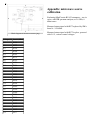
Appendix: microwave source
calibration
Evaluating MiniCircuits RVA33 attenuator -- two in
series, with IFR spectrum analyzer, at 2.0 GHz, 0
dBm source.
Measured return signal with DUT replaced by SMA
barrel is -3.58 dBm.
Block diagram of microwave source (png)
Voltage (V) Level (-dBm)
0.0
0.1
80.94
83.72
0.2
83.58
0.3
83.94
0.4
83.91
0.5
0.6
83.75
83.22
0.7
81.20
0.8
71.94
0.9
54.36
1.0
1.1
42.08
35.50
1.2
31.13
1.3
28.34
1.4
26.24
1.5
1.6
24.69
23.56
1.7
22.66
1.8
21.88
1.9
21.18
2.0
2.1
20.55
20.11
2.2
19.61
2.3
19.15
2.4
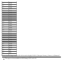
18.77
Measured return signal with DUT in place, powered
with 5.0 V, various control voltages:
2.5
2.6
18.38
18.03
2.7
17.63
2.8
17.27
2.9
16.94
3.0
3.1
16.58
16.20
3.2
15.84
3.3
15.48
3.4
15.11
3.5
3.6
14.81
14.45
3.7
14.09
3.8
13.72
3.9
13.33
4.0
4.1
12.91
12.66
4.2
12.19
4.3
11.86
4.4
11.44
4.5
4.6
11.10
10.69
4.7
10.20
4.8
9.83
4.9
9.50
5.0
9.15
Retrieved from "https://coursewikis.fas.harvard.edu/phys191r/D-4_Nitrogen-Vacancy_Centers_in_Diamond"
This page was last modified on 28 February 2013, at 16:19.