1
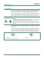
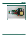
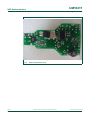
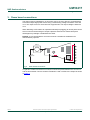
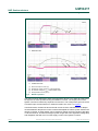
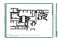
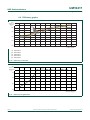
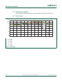
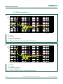
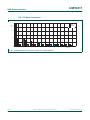
UM10417
Demo board for mains 17 W LED driver and dimmer using the
SSL2102
Rev. 1 — 30 September 2010
User manual
Document information
Info
Content
Keywords
SSL2102, AC mains supply, dimmable LED driver, AC/DC conversion
Abstract
This User manual describes a demonstration (demo) board for evaluating
an AC mains LED driver with a dimmer for 17 W, PAR38 LEDs using the
SSL2102. It also describes key features and connections to aid the design
of LED drivers for typical applications.
UM10417
NXP Semiconductors
Demo board for mains 17 W LED driver and dimmer using the SSL2102
Revision history
Rev
Date
Description
1
20100930
Initial version
Contact information
For more information, please visit: http://www.nxp.com
For sales office addresses, please send an email to: [email protected]
UM10417
User manual
All information provided in this document is subject to legal disclaimers.
Rev. 1 — 30 September 2010
© NXP B.V. 2010. All rights reserved.
2 of 23
UM10417
NXP Semiconductors
Demo board for mains 17 W LED driver and dimmer using the SSL2102
1. Introduction
This User manual describes a demonstration (demo) board for evaluating an AC mains
LED driver with a dimmer for 17 W, PAR38 LEDs using the SSL2102. It describes key
features and connections to aid the design of LED drivers for typical applications.
The demo board operates from an AC mains voltage of 120 V AC (60 Hz). The resulting
design is a trade-off between high power factor, efficiency and dimmer compatibility,
combined with high output stability and ElectroMagnetic Compliance (EMC) compliance.
WARNING
Lethal voltage and fire ignition hazard
The non-insulated high voltages that are present when operating this product, constitute a
risk of electric shock, personal injury, death and/or ignition of fire.
This product is intended for evaluation purposes only. It shall be operated in a designated test
area by personnel qualified according to local requirements and labor laws to work with
non-insulated mains voltages and high-voltage circuits. This product shall never be operated
unattended.
The demo board is powered by AC mains voltage. Avoid touching the board when power
is applied. An isolated housing is obligatory when used in uncontrolled, non-laboratory
environments.
The secondary circuit with LED connection has galvanic isolation, however this isolation is
not in accordance with any standard and has not been thoroughly tested. Thus it is
recommended to always provide galvanic isolation of the mains phase using a variable
transformer. Isolated and non-isolated devices are identified by the following symbols.
isolated
non-isolated
019aaa546
019aaa547
a. Isolated
Fig 1.
b. Non-isolated
Isolated and non-isolated symbols
UM10417
User manual
All information provided in this document is subject to legal disclaimers.
Rev. 1 — 30 September 2010
© NXP B.V. 2010. All rights reserved.
3 of 23
UM10417
NXP Semiconductors
Demo board for mains 17 W LED driver and dimmer using the SSL2102
2. Specification
Table 1.
Demo board specification
Parameter
Value
Comment
AC line input voltage
0 V to 150 V AC, 60 Hz
120 V AC model
Output voltage (LED voltage)
17 V to 33 V DC
Output voltage protection
33 V DC
Output current (LED current)
600 mA typical
Input voltage/load current dependency
−2.7 % to +3.2 %, input voltage from
110 V to 150 V AC
Output voltage/load current dependency −8.9 % to +9.1 %, output voltage from
19 V to 30 V DC
see Figure 7 on page 14
see Figure 7 on page 14
Temperature stability
−1.9 % to +2.4 % from 100 °C to
−20 °C; acceleration life test of IC over
75,000 hours
Current ripple
±15 % at 550 mA
typical value
Maximum output power (LED power)
19 W
depends on load
Efficiency
76 % to 82 %
at Tamb = 25 °C, depends on output load
and input voltage; see Figure 10 on
page 18 and Figure 11 on page 18
Power factor at input voltage of
120 V AC
>0.95
see Figure 12 on page 19
Switching frequency
40 kHz to 60 kHz
at 120 V AC input voltage
Dimming range
100 % to 0 %
for triac dimmer
Board dimensions
82 mm × 62 mm × 35 mm
LXBXH
Operating temperature
0 °C to 105 °C
EMC Compliance
FCC15 and IEC 61000-3-2
pre-compliant
EN 55015 and IEC 61000-3-2
pre-compliant
UM10417
User manual
All information provided in this document is subject to legal disclaimers.
Rev. 1 — 30 September 2010
at 120 V AC input voltage; see
Figure 13 on page 20 and Figure 14 on
page 20
© NXP B.V. 2010. All rights reserved.
4 of 23
UM10417
NXP Semiconductors
Demo board for mains 17 W LED driver and dimmer using the SSL2102
019aaa548
Fig 2.
UM10417
User manual
Demo board (top view)
All information provided in this document is subject to legal disclaimers.
Rev. 1 — 30 September 2010
© NXP B.V. 2010. All rights reserved.
5 of 23
UM10417
NXP Semiconductors
Demo board for mains 17 W LED driver and dimmer using the SSL2102
019aaa549
Fig 3.
UM10417
User manual
Demo board (bottom view)
All information provided in this document is subject to legal disclaimers.
Rev. 1 — 30 September 2010
© NXP B.V. 2010. All rights reserved.
6 of 23
UM10417
NXP Semiconductors
Demo board for mains 17 W LED driver and dimmer using the SSL2102
3. Demo board connections
The demo board is optimized for an AC mains source of 120 V (60 Hz). It is designed to
work with multiple high power LEDs having a total working voltage of between 18 V and
33 V. The output current is set to 600 mA at typical load. The output voltage is limited to
33 V.
When attaching a LED load to an operational board (hot plugging) an inrush peak current
will occur due to the discharge of output capacitors C9 and C10. Note that frequent
discharges may damage or deteriorate the LEDs.
Remark: It is recommended to mount the board in a shielded or isolated box for
demonstration purposes.
dimmer
L
AC
mains
019aaa550
Fig 4.
Demo board connections
If a galvanic isolated transformer is used, this should be placed between the AC source
and the demo board. Connect a series of between 5 and 10 LEDs to the output as shown
in Figure 4.
UM10417
User manual
All information provided in this document is subject to legal disclaimers.
Rev. 1 — 30 September 2010
© NXP B.V. 2010. All rights reserved.
7 of 23
UM10417
NXP Semiconductors
Demo board for mains 17 W LED driver and dimmer using the SSL2102
4. Dimmers
NXP Semiconductors has tested the performance of several triac-based dimmers having
different specifications. The range of dimmers which have been tested with the demo
board are given in Table 2.
Table 2.
Tested dimmers
An incandescent lamp is used as load.
Manufacturer
Type
AC Voltage
(V)
Power range
(W)
Low dim level
(%)
Lutron
TG-600PH-WH
120
600
0
Levitron
L12-6641-W
120
600
0
Levitron
L02-700-W
120
600
0
Levitron
6602-IW
120
600
0
Levitron
6683-W
120
600
0
Levitron
R12-6631-LW
120
600
0
Cooper
6001
120
600
0
Lutron
S-600PH
120
600
0
GE
18019
120
600
0
GE
18025
120
600
0
GE
52129
120
600
0
019aaa551
800
output
current
(mA)
600
(1)
(2)
(3)
(4)
(5)
(6)
400
200
0
40
60
80
100
120
140
160
AC input voltage (V)
The output current can be set at a fixed maximum of 590 mA with 5 LEDs as shown by curve (1).
(1) 5 LEDs.
(2) 6 LEDs.
(3) 7 LEDs.
(4) 8 LEDs.
(5) 9 LEDs.
(6) 10 LEDs.
Fig 5.
Typical AC input voltage dimming curves
UM10417
User manual
All information provided in this document is subject to legal disclaimers.
Rev. 1 — 30 September 2010
© NXP B.V. 2010. All rights reserved.
8 of 23
UM10417
NXP Semiconductors
Demo board for mains 17 W LED driver and dimmer using the SSL2102
5. Functional description
Refer to Figure 7 “Demo board 120 V AC schematic” on page 14. The AC mains LED
driver IC SSL2102 controls and drives a flyback converter circuit and ensures correct
dimmer operation. The IC has three integrated high voltage switches, one of which,
located between pins DRAIN and SOURCE, controls flyback input power. When the
switch opens, a current flows which is stored as energy in transformer TX1. This current is
interrupted, either when the duty factor exceeds the 75 % maximum level set by pin
PWMLIMIT, or when the voltage on pin SOURCE exceeds 0.5 V. In the next cycle, the
energy stored in the transformer discharges via D6 to output capacitors C9 and C10 and
finally absorbed by the load. The flyback converter frequency is set by an internal
oscillator whose timing is controlled by external RC components connected to pins RC
and RC2. The frequency can be set by pin BRIGHTNESS to an upper or a lower value.
The flyback converter frequency range is set by the ratio between R11 and R12.
The two other switches in the IC are called weak-bleeder (pin WBLEED) and
strong-bleeder (pin SBLEED). When the voltage on both these pins is below a certain
value, typically 52 V, the strong-bleeder switches on to provide a path for load current to
the dimmer during zero voltage crossing, resetting the dimmer timer. When the voltage on
both pins is above 52 V and the voltage on pin ISENSE is above −100 mV, the
weak-bleeder is switched on by transistor Q3. This supplies a boosted (hold) current to
the dimmer to maintain stable latching during the periods when the flyback converter
draws insufficient current.
Figure 6 shows the bleeder voltage against time in dimmed and undimmed modes.
UM10417
User manual
All information provided in this document is subject to legal disclaimers.
Rev. 1 — 30 September 2010
© NXP B.V. 2010. All rights reserved.
9 of 23
UM10417
NXP Semiconductors
Demo board for mains 17 W LED driver and dimmer using the SSL2102
(1)
(2)
(3)
(4)
019aaa552
a. Dimmed mode
(1)
(2)
(3)
(4)
019aaa553
b. Undimmed mode
(1) Demo board input current (Iin).
(2) Rectified AC mains voltage (Vin) after bridge BD1.
(3) Q3 Collector voltage (VQ3coll), weak-bleeder action.
(4) Strong-bleeder current (Sbleed).
Fig 6.
Bleeder operation
The demo board is optimized to work at a power factor above 0.9. In order to achieve this,
the flyback converter operates during the MOSFET on-time. The output power of the
flyback converter is buffered by capacitors C9 and C10. This configuration gives the circuit
a resistive input current behavior in undimmed mode; see curve Iin in Figure 6.
In dimmed mode, the dimmer latch and hold current must be maintained and a damper
must be added to dampen the inrush current and dissipate the electric power stored in the
dimmer’s LC filter. A serial resistor can be used as a damper at power ranges of less than
10 W, this however, is inefficient at higher power ranges due to the significant voltage drop
and dissipation that will occur from the supply current to the flyback converter.
UM10417
User manual
All information provided in this document is subject to legal disclaimers.
Rev. 1 — 30 September 2010
© NXP B.V. 2010. All rights reserved.
10 of 23
UM10417
NXP Semiconductors
Demo board for mains 17 W LED driver and dimmer using the SSL2102
Darlington transistor Q4 provides the necessary high gain and will be in saturation as long
as its base voltage is above the emitter voltage plus the base-emitter voltage (VBE). The
voltage across emitter resistor R14 increases with the current. When the emitter voltage
rises above the threshold, Q4 stops saturation, turns off, and the current is then limited by
R15. The values of D9 and R13 affect efficiency and power factor and must be chosen
with care to ensure consistent operation over the input voltage range from 120 V to
230 V AC.
A combination of serial resistance and a parallel damper is chosen. The serial resistance
comprises R14, R15 and R17. The parallel group damper comprises C1, C13 and R1 in
parallel with C8 and R7 for optional fine tuning. To improve efficiency, the major serial
damping is activated only when there is a peak inrush current (active inrush current
limiter). In normal operation, Darlington transistor Q4 conducts, bypassing R15 and
lowering ohmic losses. When a high inrush current is detected, Q4 starts to clip at its
maximum current of 600 mA.
The flyback converter input circuit must have a filter that is partially capacitive. C2, L2, C3,
C13 and L1 form a filter that blocks most of the disturbance generated by the flyback
converter input current. The drawback of this filter is a reduced power factor due to the
capacitive load. A lower flyback converter power relative to the capacitive value of this
filter/buffer reduces the power factor. With the 120 V AC design using 330 nF capacitors,
a minimum power factor of 0.98 is achieved.
The demo board has a feedback loop to limit the output current. The feedback loop
senses the LED current through sense resistor R25, and current mirror circuit with IC4.
The current level can be set using R27 and R29. The same feedback loop is also used for
overvoltage protection. If the LED voltage exceeds 36 V, a current starts to flow through
R23 and D11. The current through the optocoupler IC3 forces pins PWMLIMIT and
BRIGHTNESS LOW. At a value below 400 mV, the MOSFET on-time is zero.
The feedback loop has proportional action only, and the gain is critical because of phase
shift caused by the flyback converter and C6.
The relationship between pin PWMLIMIT and the output current is quadratic in nature.
The resulting output current spread will be acceptable for most LED applications. If higher
demands are placed on LED current spread, a secondary regulation circuit in combination
with an added pure current action control is advisable.
The dimming range is detected by sensing the average rectified voltage. R2 and R10 form
a voltage divider, and C4 filters the resulting signal. The flyback converter sets its duty
factor and converter frequency accordingly.
UM10417
User manual
All information provided in this document is subject to legal disclaimers.
Rev. 1 — 30 September 2010
© NXP B.V. 2010. All rights reserved.
11 of 23
UM10417
NXP Semiconductors
Demo board for mains 17 W LED driver and dimmer using the SSL2102
6. System optimization
The modifications described in this section can be applied to achieve customer application
specifications.
6.1 Changing output voltage and LED current
One of the major advantages of a flyback converter over other topologies is its suitability
for driving different output voltages. In essence, changing the winding ratio whilst
maintaining the value of the primary inductance will shift the output working voltage
accordingly. Part of the efficiency of the driver is linked to the output voltage. A lower
output voltage will increase transformation ratio and cause higher secondary losses. In
practice, a mains dimmable flyback converter will have an efficiency of between 85 % for
higher output power and voltage such as 60 V, down to 60 % for lower output power and
voltage such as 1 W and 3 V respectively. At lower voltages, synchronous rectification
may be advisable to reduce losses after high current is rectified; synchronous rectification
controllers TEA1761 and TEA1791 from NXP Semiconductors can be used for this
purpose. Calculations for transformer properties and peak current are described in detail
in application note AN10754, SSL2101 and SSL2102 dimmable mains LED driver. The
output voltage protection is set by the value of D11. Changing the value of D11 allows the
the LED driver to be adapted to a specific output load and to reduce the load’s hot swap
inrush current.
6.2 Changing the output ripple current
The output ripple current is mainly determined by the LED voltage, the LED dynamic
resistance and the output capacitor. Whilst the values of C9 and C10 are chosen to
optimize capacitor size with LED brightness. A ripple of ±15 % will result in an expected
deterioration of LED brightness of less than 1 %1.
The size of the buffer capacitor can be determined from Equation 1.
1
led⎞
⎛ C10 + C9 = I------- × -------------------------------------------⎝
ΔI ⎠ 6 × f net × R dynamic
(1)
Example: with a ripple current of ±5 %, AC mains frequency of 50 Hz, and a dynamic
20
resistance of 0.6 Ω, the resultant value of C9 + C10 is ---------------------- = 111 μF.
300 × 0.6
With a ripple current of 25 % and a dynamic resistance of 6 Ω, the resultant value of C9 +
4
C10 is ------------------ = 2200 μF.
300 × 6
Using a series of LEDs, the dynamic resistance of each LED can be added to the total
dynamic resistance.
1.
M. Weiland 28-07-2006
UM10417
User manual
All information provided in this document is subject to legal disclaimers.
Rev. 1 — 30 September 2010
© NXP B.V. 2010. All rights reserved.
12 of 23
UM10417
NXP Semiconductors
Demo board for mains 17 W LED driver and dimmer using the SSL2102
6.3 Adapting to high power reverse phase (transistor) dimmers
Reverse phase (transistor) dimmers differ in two ways that can be beneficial:
• Because of the negative phase, there is no inrush current when the dimmer triggers.
With triac dimmers, there is a sudden voltage difference over the input, resulting in a
steep charge of the input capacitors. The resulting peak current results in higher
damper dissipation. With transistor dimmers, this steep charge is missing, the input
capacitors will have less stress and the input circuit is less prone to audible noise.
• Transistor dimmers contain active circuitry that require a load charge during the time
that the dimmer is open. The dimensioning of the circuit generating the internal supply
voltage inside the dimmer is made critical in order to avoid internal dimmer losses.
This means that the remaining voltage drop across the lamp must be low enough to
allow this charge to be reached. The minimum load to achieve such a voltage drop
would result in very inefficient operation at low output power levels since most of the
energy is wasted driving the dimmer instead of producing light.
On the demo board, the weak-bleeder resistor values of R3 and R4 are chosen so that
losses are within acceptable limits and only occur in dimmed mode at the end of the
phase. The voltage drop in some transistor dimmers is however not sufficient to allow full
control of the dimming range, whereas the SSL2102 senses the dimming range by taking
the average rectified voltage as input. To compensate for the reduced voltage difference,
the voltage detection can be made more sensitive by placing a Zener diode in series with
R2. Because of increased sensitivity, the dimming curve will be steeper and shifted when
using triac dimmers.
6.4 Changing the output current
The output current can be set initially by varying the values of R29 and R27. The power
section and transformer train can withstand output currents up to 700 mA, but losses will
increase with higher current levels. Note that resistors R19A/B limit the primary peak
current and thus the maximum output power.
UM10417
User manual
All information provided in this document is subject to legal disclaimers.
Rev. 1 — 30 September 2010
© NXP B.V. 2010. All rights reserved.
13 of 23
xxxx xxxxxxxxxxxxxxxxxxxxxxxxxxxxxx x xxxxxxxxxxxxxx xxxxxxxxxx xxx xxxxxx xxxxxxxxxxxxxxxxxxxxxxx xxxxxxxxxxxxxxxxxxxxxx
xxxxx xxxxxx xx xxxxxxxxxxxxxxxxxxxxxxxxxxxxx xxxxxxxxxxxxxxxxxxxxxx xxxxxxxxxxx xxxxxxx xxxxxxxxxxxxxxxxxxx
xxxxxxxxxxxxxxxx xxxxxxxxxxxxxx xxxxxx xx xxxxxxxxxxxxxxxxxxxxxxxxxxxxxxxx xxxxxxxxxxxxxxxxxxxxxxxx xxxxxxx
xxxxxxxxxxxxxxxxxxxxxxxxxxxxxxxxxxxxxxxxxxxxxx xxxxxxxxxxx xxxxx x x
R1
2.2 kΩ
2W
BD1
D3
BC1
RGND
C1
100 nF
250 V
N
VACT
D1
(1)
D6
L2
L1
680 μH
FerCoil
C2
0.33 μF
1
C3
0.33 μF
C8
(1)
R7
(1)
R4
2.2 kΩ/3 W
Q3
PNP-TO92
D4
180 V
3W
2
3
TX1 6
L3
100 μH
C9
1000 μF
35 V
DIODE04/05
N1
N4, N5
N2
R25
8
SGND
6.8 kΩ//6.8 kΩ//6.8 kΩ
D5
R5
4.7 kΩ/2 W
10 kΩ//10 kΩ
SBLEED
RGND
GND
GND
R9
R8
WBLEED
51 kΩ
10 kΩ
VCC
VCC
R10
15 kΩ
C4
4.7 μF
50 V
R11
8.2 kΩ
R12
100 kΩ
3
18
4
17
SSL2102
7
BRIGHTNESS
7.5 kΩ
19
6
GND
R6
20
2
5
GND
R2
700 kΩ
D10
1
RC2
RC
16
15
14
8
13
9
12
10
11
DRAIN
GND
R19A
GND
1Ω
RGND
IC3-B
R26
SGND
0.75 Ω
GND
R27
51 kΩ
10 kΩ
2
R29
1 3.9 kΩ
C12
100 μF
16 V
IC4
BCM61B
3
R19B
SOURCE
4
R32
1 kΩ
SGND
R21
AUX
100 kΩ
ISENSE
R22
PWMLIMIT
10 Ω
D7
C5
330 pF
VCC
R13
R16
82 kΩ
Q4
D9
ZD
4.3 V
R30
R31
1 kΩ
GND
390 kΩ
C6
100 nF
63 V
R24
6.8 kΩ
0Ω
GND
IC3-A
VACT
R23
10 kΩ
D11
ZD33
IC1
−
0.22 Ω/0.25 W
R20
1 kΩ
R18
100 kΩ
NPN
D8
ZD
33 V
C8A
10 μF
50 V
4
5
N3
C7
100 nF
R14
R15
R17
C11
3.3 Ω/2 W
10 Ω//10 Ω//10 Ω
220 Ω/2 W
470 Ω//470 Ω
6.8 Ω/2 W
20 Ω//20 Ω
2.2 nF/400 V AC
SGND
019aaa554
Some resistor values are shown with format x/x/x which represent the values required of resistors connected in parallel.
Fig 7.
Demo board 120 V AC schematic
UM10417
14 of 23
© NXP B.V. 2010. All rights reserved.
(1) Optional.
Demo board for mains 17 W LED driver and dimmer using the SSL2102
Rev. 1 — 30 September 2010
All information provided in this document is subject to legal disclaimers.
R3
2.2 kΩ
6.8 kΩ//6.8 kΩ//6.8 kΩ
+
C10
1000 μF
35 V
NXP Semiconductors
C13
2.2 nF
250 V
7. Demo board schematic
UM10417
User manual
L
UM10417
NXP Semiconductors
Demo board for mains 17 W LED driver and dimmer using the SSL2102
8. PCB components
Table 3.
Demo board 120 V AC components
Designator Description
Part identifier
Manufacturer
R1
2.2 kΩ, 2 W, 5 %, 200 V, SMD, 2512
-
-
R2
700 kΩ, 0.25 W, 1 %, 200 V, SMD, 1206
-
-
R3, R4
2.2 kΩ, 3 W, 5 %, 400 V, SMD, 2512
-
-
R5
4.7 kΩ, 2 W, 5 %, 400 V, SMD, 2512
-
-
R6
7.5 kΩ, 0.125 W, 5 %, SMD, 0805
-
-
R8
10 kΩ, 0.125 W, 5 %, SMD, 0805
-
-
R9
51 kΩ, 0.25 W, 5 %, 200 V, SMD, 1206
-
-
R10
15 kΩ, 0.125 W, 1 %, SMD, 0805
-
-
R11
8.2 kΩ, 0.125 W, 1 %, SMD, 0805
-
-
R12, R18
100 kΩ, 0.125 W, 1 %, SMD, 0805
-
-
R13
390 kΩ, 2 W, 5 %, DIP
-
-
R14
3.3 Ω, 3 W, 5 %, 400 V, SMD, 2512
-
-
R15
220 Ω, 2 W, 5 %, 400 V, SMD, 2512
-
-
R16
82 kΩ, 0.125 W, 1 %, SMD, 0805
-
-
R17
6.8 Ω, 2 W, 5 %, 400 V, SMD, 2512
-
-
R18
100 kΩ, 0.125 W, 1 %, SMD, 0805
-
-
R19A
1 Ω, 0.25 W, 1 %, SMD, 1206
-
-
R19B
0.75 Ω, 0.25 W, 1 %, SMD, 1206
-
-
R20
1 kΩ, 0.125 W, 1 %, SMD, 0805
-
-
R21
100 kΩ, 0.125 W, 5 %, SMD, 0805
-
-
R22
10 Ω, 0.125 W, 5 %, SMD, 0805
-
-
R23
10 kΩ, 0.125 W, 5 %, SMD, 0603
-
-
R24
6.8 kΩ, 0.125 W, 5 %, SMD, 0603
-
-
R25
0.22 Ω, 0.25 W, 1 % DIP
-
-
R26
10 kΩ, 0.125 W, 1 %, SMD, 0603
-
-
R27
51 kΩ, 0.125 W, 1 %, SMD, 0603
-
-
R29
3.9 kΩ, 0.125 W, 1 %, SMD, 0603
-
-
R30
0 Ω, 0.125 W, 5 %, SMD, 0603
-
-
R31
1 kΩ, 0.125 W, 5 %, SMD, 0603
-
-
R32
1 kΩ, 0.125 W, 1%, SMD, 0603
-
-
C1
100 nF, MKT, 10 %, 400 V
-
-
C2, C3
330 nF, MKT, 10 %, 400 V
-
-
C4
4.7 uF, 105 °C, 10 %, 50 V
-
-
C5
330 pF, Cer, 10 %,50 V, SMD, 0603
-
-
C6
100 nF, MKT, 10 %, 63 V
-
-
C7
100 nF, Cer, 10 %, 50 V, SMD
-
-
C8A
10 μF, 105 °C, 10 %, 50 V
-
-
C9, C10
1000 μF, 105 °C, 20 %, 35 V
MCRH35V108, M13X21
Multicomp
C11
2.2 nF, Y, 20 %, 400 V
-
-
UM10417
User manual
All information provided in this document is subject to legal disclaimers.
Rev. 1 — 30 September 2010
© NXP B.V. 2010. All rights reserved.
15 of 23
UM10417
NXP Semiconductors
Demo board for mains 17 W LED driver and dimmer using the SSL2102
Table 3.
Demo board 120 V AC components …continued
Designator Description
Part identifier
Manufacturer
C12
100 μF, 105 °C, 20 %, 16 V
-
-
C13
2.2 nF, MKT, 10 %, 250 V
-
-
L2
680 μH, 10 %, SMD, WE-PD2
744776268
Wurth
L3
100 μH, 10 %, SMD, WE-PD
74477720
Wurth
TX1
transformer, 1m, E25-25-8
750340772
WE-Midcom
BD1
rectifier bridge, SMD, DB107S
-
-
D1
TVS diode, P6KE250 (optional)
-
-
D3
diode, HER107
-
-
D4
Zener, 3 W, 180 V, BZT03C180
-
-
D5
diode, HER107
-
-
D6
diode, HER303
-
-
D7
diode, SMD, BAS16J
-
NXP
D8
Zener, 33 V, SMD, SOD66, BZX84J-B33
-
NXP
D9
Zener, 4.3 V, SMD, SOD80C, BZX84J-B4V3
-
NXP
D10
diode, SMD, BAS16J
-
NXP
D11
Zener, 33 V, SMD, SOD66, BZX84J-B33
-
NXP
Q3
transistor, PNP, TO-92, MPSA92
-
-
Q4
transistor, NPN, TO-220, ST901T
-
-
IC1
controller, SMD, SOW-20, SSL2102
SSL2102
NXP
IC3
optocoupler, SMD, SO-4, PC817
PC817
-
IC4
dual, NPN, SMD, SOT143B, BCM61B
BCM61B
NXP
UM10417
User manual
All information provided in this document is subject to legal disclaimers.
Rev. 1 — 30 September 2010
© NXP B.V. 2010. All rights reserved.
16 of 23
UM10417
NXP Semiconductors
Demo board for mains 17 W LED driver and dimmer using the SSL2102
9. Test results
9.1 Input/output stability
019aaa555
700
output
current
(mA)
600
(1)
(2)
(3)
(4)
(5)
500
400
15.5
18.5
21.5
24.5
27.5
30.5
33.5
DC output voltage (V)
(1) Test board A.
(2) Test board B.
(3) Test board C.
(4) Test board D.
(5) Test board E.
Fig 8.
Input voltage stability
019aaa556
800
output
current
(mA)
600
400
200
0
40
Fig 9.
60
80
100
120
140
150
AC input voltage (V)
Output voltage stability with 5 LEDs
UM10417
User manual
All information provided in this document is subject to legal disclaimers.
Rev. 1 — 30 September 2010
© NXP B.V. 2010. All rights reserved.
17 of 23
UM10417
NXP Semiconductors
Demo board for mains 17 W LED driver and dimmer using the SSL2102
9.2 Efficiency graphs
019aaa557
81.5
efficiency at
120 V AC
(%)
80.5
(1)
(2)
(3)
(4)
(5)
79.5
78.5
77.5
76.5
4
5
6
7
8
9
10
number of LEDs
(1) Test board A.
(2) Test board B.
(3) Test board C.
(4) Test board D.
(5) Test board E.
Fig 10. Efficiency at 120 V AC
019aaa558
90
efficiency at
typical load
(%)
70
50
30
10
40
60
80
100
120
140
160
AC input voltage (V)
Fig 11. Efficiency at typical load
UM10417
User manual
All information provided in this document is subject to legal disclaimers.
Rev. 1 — 30 September 2010
© NXP B.V. 2010. All rights reserved.
18 of 23
UM10417
NXP Semiconductors
Demo board for mains 17 W LED driver and dimmer using the SSL2102
9.3 Temperature stability
The temperature stability depends on the LED heatsink and the lamp’s form factor.
9.4 Power factor
019aaa559
1.00
power
factor
(2)
(3)
(4)
(5)
(6)
0.95
0.90
(1)
0.85
0.80
20.0
21.5
23.0
24.5
26.0
27.5
29.0
DC output voltage (V)
(1) 5 LEDs.
(2) 6 LEDs.
(3) 7 LEDs.
(4) 8 LEDs.
(5) 9 LEDs.
(6) 10 LEDs.
Fig 12. Power factor
UM10417
User manual
All information provided in this document is subject to legal disclaimers.
Rev. 1 — 30 September 2010
© NXP B.V. 2010. All rights reserved.
19 of 23
UM10417
NXP Semiconductors
Demo board for mains 17 W LED driver and dimmer using the SSL2102
9.5 EMC Pre-compliance
019aaa560
100
level
(dBμV)
80
60
(3)
(2)
(4)
40
(1)
20
0
10−2
10−1
1
102
10
f (MHz)
(1) Average.
(2) Peak value.
(3) EN 55015 peak upper limit.
(4) EN 55015 average upper limit.
Fig 13. EMC Pre-compliance, L phase against EN 55015 and peak
019aaa561
100
level
(dBμV)
80
60
(3)
(2)
(4)
40
(1)
20
0
10-2
10-1
1
102
10
f (MHz)
(1) Average.
(2) Peak value.
(3) EN 55015 peak upper limit.
(4) EN 55015 average upper limit.
Fig 14. EMC Pre-compliance, N phase against EN 55015 and peak
UM10417
User manual
All information provided in this document is subject to legal disclaimers.
Rev. 1 — 30 September 2010
© NXP B.V. 2010. All rights reserved.
20 of 23
UM10417
NXP Semiconductors
Demo board for mains 17 W LED driver and dimmer using the SSL2102
9.6 AC Mains harmonics
019aaa562
30
Class C
level
(%)
650 mA
20
10
0
2
6
10
14
18
harmonic
Fig 15. AC Mains harmonics at 650 mA output current (IEC 61000-3-2)
UM10417
User manual
All information provided in this document is subject to legal disclaimers.
Rev. 1 — 30 September 2010
© NXP B.V. 2010. All rights reserved.
21 of 23
UM10417
NXP Semiconductors
Demo board for mains 17 W LED driver and dimmer using the SSL2102
10. Legal information
10.1 Definitions
Draft — The document is a draft version only. The content is still under
internal review and subject to formal approval, which may result in
modifications or additions. NXP Semiconductors does not give any
representations or warranties as to the accuracy or completeness of
information included herein and shall have no liability for the consequences of
use of such information.
10.2 Disclaimers
Limited warranty and liability — Information in this document is believed to
be accurate and reliable. However, NXP Semiconductors does not give any
representations or warranties, expressed or implied, as to the accuracy or
completeness of such information and shall have no liability for the
consequences of use of such information.
In no event shall NXP Semiconductors be liable for any indirect, incidental,
punitive, special or consequential damages (including - without limitation - lost
profits, lost savings, business interruption, costs related to the removal or
replacement of any products or rework charges) whether or not such
damages are based on tort (including negligence), warranty, breach of
contract or any other legal theory.
Notwithstanding any damages that customer might incur for any reason
whatsoever, NXP Semiconductors’ aggregate and cumulative liability towards
customer for the products described herein shall be limited in accordance
with the Terms and conditions of commercial sale of NXP Semiconductors.
Right to make changes — NXP Semiconductors reserves the right to make
changes to information published in this document, including without
limitation specifications and product descriptions, at any time and without
notice. This document supersedes and replaces all information supplied prior
to the publication hereof.
Suitability for use — NXP Semiconductors products are not designed,
authorized or warranted to be suitable for use in life support, life-critical or
safety-critical systems or equipment, nor in applications where failure or
malfunction of an NXP Semiconductors product can reasonably be expected
to result in personal injury, death or severe property or environmental
damage. NXP Semiconductors accepts no liability for inclusion and/or use of
NXP Semiconductors products in such equipment or applications and
therefore such inclusion and/or use is at the customer’s own risk.
Applications — Applications that are described herein for any of these
products are for illustrative purposes only. NXP Semiconductors makes no
representation or warranty that such applications will be suitable for the
specified use without further testing or modification.
Customers are responsible for the design and operation of their applications
and products using NXP Semiconductors products, and NXP Semiconductors
accepts no liability for any assistance with applications or customer product
UM10417
User manual
design. It is customer’s sole responsibility to determine whether the NXP
Semiconductors product is suitable and fit for the customer’s applications and
products planned, as well as for the planned application and use of
customer’s third party customer(s). Customers should provide appropriate
design and operating safeguards to minimize the risks associated with their
applications and products.
NXP Semiconductors does not accept any liability related to any default,
damage, costs or problem which is based on any weakness or default in the
customer’s applications or products, or the application or use by customer’s
third party customer(s). Customer is responsible for doing all necessary
testing for the customer’s applications and products using NXP
Semiconductors products in order to avoid a default of the applications and
the products or of the application or use by customer’s third party
customer(s). NXP does not accept any liability in this respect.
Export control — This document as well as the item(s) described herein
may be subject to export control regulations. Export might require a prior
authorization from national authorities.
Evaluation products — This product is provided on an “as is” and “with all
faults” basis for evaluation purposes only. NXP Semiconductors, its affiliates
and their suppliers expressly disclaim all warranties, whether express, implied
or statutory, including but not limited to the implied warranties of
non-infringement, merchantability and fitness for a particular purpose. The
entire risk as to the quality, or arising out of the use or performance, of this
product remains with customer.
In no event shall NXP Semiconductors, its affiliates or their suppliers be liable
to customer for any special, indirect, consequential, punitive or incidental
damages (including without limitation damages for loss of business, business
interruption, loss of use, loss of data or information, and the like) arising out
the use of or inability to use the product, whether or not based on tort
(including negligence), strict liability, breach of contract, breach of warranty or
any other theory, even if advised of the possibility of such damages.
Notwithstanding any damages that customer might incur for any reason
whatsoever (including without limitation, all damages referenced above and
all direct or general damages), the entire liability of NXP Semiconductors, its
affiliates and their suppliers and customer’s exclusive remedy for all of the
foregoing shall be limited to actual damages incurred by customer based on
reasonable reliance up to the greater of the amount actually paid by customer
for the product or five dollars (US$5.00). The foregoing limitations, exclusions
and disclaimers shall apply to the maximum extent permitted by applicable
law, even if any remedy fails of its essential purpose.
10.3 Trademarks
Notice: All referenced brands, product names, service names and trademarks
are the property of their respective owners.
All information provided in this document is subject to legal disclaimers.
Rev. 1 — 30 September 2010
© NXP B.V. 2010. All rights reserved.
22 of 23
UM10417
NXP Semiconductors
Demo board for mains 17 W LED driver and dimmer using the SSL2102
11. Contents
1
2
3
4
5
6
6.1
6.2
6.3
6.4
7
8
9
9.1
9.2
9.3
9.4
9.5
9.6
10
10.1
10.2
10.3
11
Introduction . . . . . . . . . . . . . . . . . . . . . . . . . . . . 3
Specification. . . . . . . . . . . . . . . . . . . . . . . . . . . . 4
Demo board connections . . . . . . . . . . . . . . . . . 7
Dimmers . . . . . . . . . . . . . . . . . . . . . . . . . . . . . . . 8
Functional description . . . . . . . . . . . . . . . . . . . 9
System optimization . . . . . . . . . . . . . . . . . . . . 12
Changing output voltage and LED current . . . 12
Changing the output ripple current . . . . . . . . . 12
Adapting to high power reverse phase (
transistor) dimmers . . . . . . . . . . . . . . . . . . . . . 13
Changing the output current . . . . . . . . . . . . . . 13
Demo board schematic . . . . . . . . . . . . . . . . . . 14
PCB components . . . . . . . . . . . . . . . . . . . . . . . 15
Test results . . . . . . . . . . . . . . . . . . . . . . . . . . . . 17
Input/output stability . . . . . . . . . . . . . . . . . . . . 17
Efficiency graphs . . . . . . . . . . . . . . . . . . . . . . 18
Temperature stability. . . . . . . . . . . . . . . . . . . . 19
Power factor . . . . . . . . . . . . . . . . . . . . . . . . . . 19
EMC Pre-compliance . . . . . . . . . . . . . . . . . . . 20
AC Mains harmonics . . . . . . . . . . . . . . . . . . . 21
Legal information. . . . . . . . . . . . . . . . . . . . . . . 22
Definitions . . . . . . . . . . . . . . . . . . . . . . . . . . . . 22
Disclaimers . . . . . . . . . . . . . . . . . . . . . . . . . . . 22
Trademarks. . . . . . . . . . . . . . . . . . . . . . . . . . . 22
Contents . . . . . . . . . . . . . . . . . . . . . . . . . . . . . . 23
Please be aware that important notices concerning this document and the product(s)
described herein, have been included in section ‘Legal information’.
© NXP B.V. 2010.
All rights reserved.
For more information, please visit: http://www.nxp.com
For sales office addresses, please send an email to: [email protected]
Date of release: 30 September 2010
Document identifier: UM10417