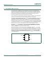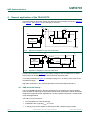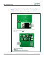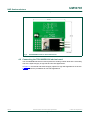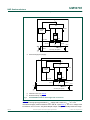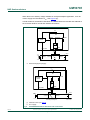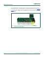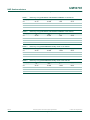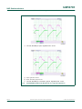
1
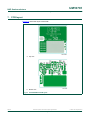
UM10781 GreenChip TEA1892DB1226 synchronous rectifier controller add-on board Rev. 1 — 20 May 2014 User manual Document information Info Content Keywords TEA1892DB1226, Synchronous Rectifier (SR) driver, high efficiency, TSOP6, flyback converter Abstract This user manual describes how the TEA1892DB1226 add-on board can be used in a flyback converter. The add-on board contains a TEA1892TS SR controller in TSOP-6 package. The add-on board also contains a power MOSFET, as well as a charge pump circuit to generate the supply voltage for the SR controller. The add-on board replaces the rectifier diode at the secondary side of the flyback converter. It is intended for high-side applications, but with minor modifications it can also be used for low-side applications. UM10781 NXP Semiconductors TEA1892DB1226 synchronous rectifier controller add-on board Revision history Rev Date Description v.1 20140520 first issue Contact information For more information, please visit: http://www.nxp.com For sales office addresses, please send an email to: [email protected] UM10781 User manual All information provided in this document is subject to legal disclaimers. Rev. 1 — 20 May 2014 © NXP B.V. 2014. All rights reserved. 2 of 22 UM10781 NXP Semiconductors TEA1892DB1226 synchronous rectifier controller add-on board 1. Introduction This document describes the TEA1892DB1226 add-on board. A functional description and a set of measurements illustrate the performance of the TEA1892DB1226 add-on board. The add-on board also contains a charge pump circuit, capable of delivering the supply voltage for the SR controller. The charge pump circuit eliminates the auxiliary transformer winding in the flyback converter. A flyback converter board in which the secondary part (diode) can be replaced by the add-on board is required to use the add-on board correctly. 2. Safety Warning WARNING Lethal voltage and fire ignition hazard The non-insulated high voltages that are present when operating this product, constitute a risk of electric shock, personal injury, death and/or ignition of fire. This product is intended for evaluation purposes only. It shall be operated in a designated test area by personnel qualified according to local requirements and labor laws to work with non-insulated mains voltages and high-voltage circuits. This product shall never be operated unattended. The board application is AC mains voltage powered. Avoid touching the board when power is applied. An isolated housing is obligatory when used in uncontrolled, non-laboratory environments. Always provide galvanic isolation of the mains phase using a variable transformer. The following symbols identify isolated and non-isolated devices. 019aab174 019aab173 a. Isolated. Fig 1. UM10781 User manual b. Non-isolated Isolated and non-isolated symbols All information provided in this document is subject to legal disclaimers. Rev. 1 — 20 May 2014 © NXP B.V. 2014. All rights reserved. 3 of 22 UM10781 NXP Semiconductors TEA1892DB1226 synchronous rectifier controller add-on board 3. TEA1892TS SR controller The TEA1892TS is a member of the new generation of Synchronous Rectifier (SR) controller ICs for switched mode power supplies. Its high level of integration allows the design of a cost-effective power supply with a very low number of external components. The IC provides synchronous rectification on the secondary side for discontinuous conduction mode and quasi-resonant mode flyback converters. It is a successor to the TEA1792TS synchronous rectifier controller IC. The TEA1892TS provides improved performance at lower loads by disabling cycle shipping. An efficient control algorithm built into the IC determines when a MOSFET is switched on or off. After a negative voltage lower than Vact(drv) (220 mV typical) is sensed on the SRSENSE pin, the driver output voltage is driven HIGH. Then the external MOSFET is switched on. When VSRSENSE rises to Vreg(drv) (42 mV/30 mV), the driver output voltage is regulated to maintain the Vreg(drv) on the SRSENSE pin. When the SRSENSE voltage is above the Vdeact(drv) level (12 mV typical), the driver output is pulled to ground. After switch-on of the SR MOSFET, the input signal on the SRSENSE pin is blanked during the tact(sr)(min) (1.5 s typical). This action eliminates false switch-off due to high frequency ringing at the start of the secondary stroke. When the secondary current is reduced until the SRSENSE voltage is Vref, the internal control loop maintains the Vreg(drv) level across the MOSFET. Maintaining Vreg(drv) in this instance is achieved when the VDRIVER voltage is decreased. This reduction enables the external power switch to be switched off quickly when the current through the switch reaches zero. The zero current is detected by sensing a Vdeact(drv) (12 mV typical) level on the SRSENSE pin. 656(16( *1' 9&& ,& '5,9(5 QF 6(/5(* DDD Fig 2. UM10781 User manual Pin configuration TEA1892TS (TSOP6) All information provided in this document is subject to legal disclaimers. Rev. 1 — 20 May 2014 © NXP B.V. 2014. All rights reserved. 4 of 22 UM10781 NXP Semiconductors TEA1892DB1226 synchronous rectifier controller add-on board 4. General application of the TEA1892TS General application diagrams of high-side and low-side rectification are given in Figure 3 and Figure 4. See Figure 2 for the relevant pin numbers. 75 4VHF 9R 9,1 5'5,9(5 &9&& *1' 5656(16( 6(/5(* '5,9(5 4SULP 35,0$5< 6,'( &21752//(5 &RXW ,& 9&& 656(16( DDD Fig 3. Application diagram for high-side rectification 75 9,1 9R 5656(16( 656(16( 9&& 4SULP 4VHF 35,0$5< 6,'( &21752//(5 5'5,9(5 &RXW ,& '5,9(5 6(/5(* *1' DDD Fig 4. Application diagram for low-side rectification In high-side rectification (Figure 3), the supply voltage for the TEA1892TS is normally derived from an auxiliary winding on the transformer secondary side. In low-side rectification (Figure 4), the output voltage VOUT is used in most cases as the TEA1892TS supply. High-side rectification is the preferred application for the best EMI performance. 4.1 Add-on board set-up The TEA1892DB1226 add-on board is designed for incorporation into existing flyback power supplies by replacing the secondary rectifier diode. Although the add-on board was designed for high-side rectifier applications, it is also possible to replace the rectifier diode in low-side applications. The add-on board consists of: • The TEA1892TS in TSOP-6 package • A MOSFET with a typical RDSon of 3.3 m • A charge pump circuit capable of delivering the SR controller supply voltage UM10781 User manual All information provided in this document is subject to legal disclaimers. Rev. 1 — 20 May 2014 © NXP B.V. 2014. All rights reserved. 5 of 22 UM10781 NXP Semiconductors TEA1892DB1226 synchronous rectifier controller add-on board Figure 5 shows the top and bottom views of the add-on board. Only the MOSFET is soldered to the front side of the add-on board. The MOSFET DRAIN (middle pin) is soldered to the large copper plane. The plane is connected via 15 interconnects to the back side of the add-on board. All the other SMD components are mounted on the back side. M2 = PSMN3R3-100PS (see Table 5). a. Top view U1 = TEA1892TS (see Table 5). b. Bottom view Fig 5. UM10781 User manual TEA1892DB1226 add-on board photographs All information provided in this document is subject to legal disclaimers. Rev. 1 — 20 May 2014 © NXP B.V. 2014. All rights reserved. 6 of 22 UM10781 NXP Semiconductors TEA1892DB1226 synchronous rectifier controller add-on board Fig 6. TEA1892DB1226 add-on board dimensions 4.2 Connecting the TEA1892DB1226 add-on board The TEA1892DB1226 add-on board replaces the existing rectifier diode at the secondary side of the flyback supply in high-side and low-side applications. In Figure 7, the internal and external supply options for high-side applications are shown. Figure 8 shows the possibilities for low-side applications. UM10781 User manual All information provided in this document is subject to legal disclaimers. Rev. 1 — 20 May 2014 © NXP B.V. 2014. All rights reserved. 7 of 22 UM10781 NXP Semiconductors TEA1892DB1226 synchronous rectifier controller add-on board 7($'% 9&& ,& *1' &+$5*( 3803 656(16( '5,9(5 *$7( 6(&*1' 6285&( FRQQHFW '5$,1 FRQQHFW ' 9287 UHPRYH' FRQQHFW VHFRQGDU\VLGHIO\EDFN DDD a. Internal charge pump supply 7($'% 9&& ,& *1' &+$5*( 3803 656(16( '5,9(5 *$7( 6(&*1' 6285&( FRQQHFW '5$,1 FRQQHFW ' 9287 UHPRYH' VHFRQGDU\VLGHIO\EDFN DDD (1) PSMN3R3-100PS (see Table 5). b. External auxiliary supply Fig 7. TEA1892DB1226 add-on board high-side connections Figure 7(a) shows the connections to be made when the internal charge pump supply is used. This charge pump generates a VCC supply with a value of VOUT 2 V. The TEA1892TS supply must be between 8.5 V and 38 V (see Ref. 1). The VOUT voltage must be between 10.5 V to 40 V. A flyback adapter output voltage is normally within this range. UM10781 User manual All information provided in this document is subject to legal disclaimers. Rev. 1 — 20 May 2014 © NXP B.V. 2014. All rights reserved. 8 of 22 UM10781 NXP Semiconductors TEA1892DB1226 synchronous rectifier controller add-on board When there is an auxiliary voltage available in the flyback adapter application, it can be used to supply the TEA1892TS VCC. See Figure 7(b). In both situations, the MOSFET SOURCE and DRAIN leads are inserted and soldered at the removed diode D1 anode and cathode connections. 7($'% 9&& ,& 656(16( *1' &+$5*( 3803 '5,9(5 *$7( 6(&*1' 6285&( '5$,1 9287 UHPRYH' FRQQHFW FRQQHFW FRQQHFW ' VHFRQGDU\VLGHIO\EDFN DDD a. Internal charge pump supply 7($'% 9&& ,& *1' &+$5*( 3803 656(16( '5,9(5 *$7( 6(&*1' 6285&( '5$,1 9287 UHPRYH' FRQQHFW FRQQHFW ' VHFRQGDU\VLGHIO\EDFN DDD (1) PSMN3R3-100PS (see Table 5). b. VOUT supply. Fig 8. UM10781 User manual TEA1892DB1226 add-on board low-side connections All information provided in this document is subject to legal disclaimers. Rev. 1 — 20 May 2014 © NXP B.V. 2014. All rights reserved. 9 of 22 UM10781 NXP Semiconductors TEA1892DB1226 synchronous rectifier controller add-on board In low-side applications, the board is easily connected. Using either the internal charge pump supply or with VOUT as the supply. The required connections are shown in Figure 8. Figure 9 shows an example of the TEA1892DB1226 add-on board used in a typical 90 W flyback adapter. Fig 9. UM10781 User manual Example of TEA1892DB1226 add-on board connected to the APBADC031 TEA1752 90 W flyback adapter All information provided in this document is subject to legal disclaimers. Rev. 1 — 20 May 2014 © NXP B.V. 2014. All rights reserved. 10 of 22 UM10781 NXP Semiconductors TEA1892DB1226 synchronous rectifier controller add-on board 5. Measurements 5.1 Introduction The performance has been measured on mainboard TEA1752 90 W flyback and PFC (see Ref. 3) with the add-on module TEA1892DB1226 connected for the high-side SR. 5.1.1 Test equipment and conditions The following test equipment is used: • • • • • • • • • AC source: Agilent 6812B Power meter: Yokogawa WT210 with harmonics option DC electronic load: Chroma, Model 63103 Digital oscilloscope: Yokogawa DL1640L Current probe Yokogawa 701933 30 A; 50 MHz 100 MHz, high-voltage differential probe: Yokogawa 700924 500 MHz, low voltage differential probe: Yokogawa 701920 Multimeter: Keithley 2000 ElectroMagnetic Compatibility (EMC) receiver: Rohde & Schwarz ESPI-3 + Line Impedance Standardization Network (LISN) ENV216 The board was tested under the following conditions: • • • • Adapter on the lab-table with heat sinks facing downwards The adapter has no casing Ambient temperature between 20 C and 25 C Measurements were made after stabilization of temperature according to "test method for calculating the efficiency of single-voltage external AC-to-DC and AC-to-AC power supplies" of ENERGY STAR 5.2 Efficiency Test conditions: The adapter is set to maximum load and preheated until temperature stabilization is achieved. Temperature stabilization is established for every load step before recording any measurements. Remark: The output voltage is measured at the output of the board. The arithmetic average of the four efficiency measurements must be ≥ 87 % for adapters, to comply with ENERGY STAR EPS2.0. Universal mains adapters must pass the criteria at both 115 V; 60 Hz and 230 V; 50 Hz. To meet this criteria, the PFC must be off at 25 % load and preferably on at 50 % load. The performance was measured with and without SR (so diode ISO MOSFET). UM10781 User manual All information provided in this document is subject to legal disclaimers. Rev. 1 — 20 May 2014 © NXP B.V. 2014. All rights reserved. 11 of 22 UM10781 NXP Semiconductors TEA1892DB1226 synchronous rectifier controller add-on board Table 1. Load (%) PIN (W) VOUT (V) Io (A) (%) 25 24.79 19.398 1.165 91.16 50 49.05 19.384 2.31 91.29 75 73.48 19.371 3.477 91.66 100 98.13 19.357 4.622 91.17 Table 2. PIN (W) VOUT (V) Io (A) (%) 25 24.90 19.399 1.165 90.76 50 50.44 19.385 2.31 88.78 75 74.14 19.372 3.477 90.85 100 97.74 19.360 4.622 91.55 Efficiency using STPS20M100S Schottky diode at 115 V/60 Hz Load (%) PIN (W) VOUT (V) Io (A) (%) 25 25.29 19.288 1.1634 88.73 50 50.24 19.257 2.3091 88.50 75 75.52 19.242 3.4709 88.44 100 101.33 19.218 4.6262 87.74 Table 4. User manual Efficiency using TEA1892TS with MOSFET PSMN3R3 at 230 V/50 Hz Load (%) Table 3. UM10781 Efficiency using TEA1892TS with MOSFET PSMN3R3 at 115 V/60 Hz Efficiency using STPS20M100S Schottky diode at 230 V/50 Hz Load (%) PIN (W) VOUT (V) Io (A) (%) 25 25.43 19.288 1.1634 88.24 50 51.56 19.265 2.3091 86.27 75 76.01 19.242 3.4709 87.87 100 100.63 19.218 4.6281 88.35 All information provided in this document is subject to legal disclaimers. Rev. 1 — 20 May 2014 © NXP B.V. 2014. All rights reserved. 12 of 22 UM10781 NXP Semiconductors TEA1892DB1226 synchronous rectifier controller add-on board DDD HIILFLHQF\ ORDGSHUFHQWDJH (1) TEA1892TS SR at 115 V; 60 Hz (2) TEA1892TS SR at 230 V; 50 Hz (3) STPS20M100S Schottky diode at 115 V; 60 Hz (4) STPS20M100S Schottky diode at 230 V; 50 Hz Fig 10. Efficiency as a function of percentage load 5.3 Operational behavior Figure 11[a] and Figure 11[b] show oscilloscope traces with the typical waveforms. The waveforms were measured when the TEA1892DB1226 SR demo board was connected to the 90 W TEA1752 adapter board as a high-side application. The two waveforms represent the gate drive voltage (purple) TEA1892TS SR controller DRIVER pin and the secondary output current (green). The output current was measured using a voltage probe directly connected over a 100 m resistor in series with the secondary side ground track. Figure 11[a] shows the waveforms for a 4 A load with the SELREG pin open. This configuration sets the regulation level at 30 mV. Figure 11[b] shows the waveforms for a 4 A load with the SELREG pin connected to ground. This configuration sets the regulation level to 42 mV) UM10781 User manual All information provided in this document is subject to legal disclaimers. Rev. 1 — 20 May 2014 © NXP B.V. 2014. All rights reserved. 13 of 22 UM10781 NXP Semiconductors TEA1892DB1226 synchronous rectifier controller add-on board a. 4 A load, SELREG pin open, regulation level 30 mV. (1) Purple: gate drive current. (2) Green: secondary output current. b. 4 A load, SELREG pin connected to ground, regulation level 42 mV. Fig 11. TEA1892DB1226 SR and 90 W TEA1752 as a high-side application UM10781 User manual All information provided in this document is subject to legal disclaimers. Rev. 1 — 20 May 2014 © NXP B.V. 2014. All rights reserved. 14 of 22 UM10781 NXP Semiconductors TEA1892DB1226 synchronous rectifier controller add-on board 5.4 Conducted EMI Tests Test conditions: • The adapter is subjected to maximum load • The ground connection of the output cable is connected to EMC ground • The gate-drive resistor (R2)value = 0 Pass criteria: CISPR22 Class-B Remark: The conducted EMI measurement result for 115 V neutral is comparable to the 115 V line. Fig 12. Conducted EMI at 115 V (AC) line UM10781 User manual All information provided in this document is subject to legal disclaimers. Rev. 1 — 20 May 2014 © NXP B.V. 2014. All rights reserved. 15 of 22 UM10781 NXP Semiconductors TEA1892DB1226 synchronous rectifier controller add-on board Remark: The conducted EMI measurement result for 230 V neutral is comparable to the 230 V line. Fig 13. Conducted EMI at 230 V (AC) line UM10781 User manual All information provided in this document is subject to legal disclaimers. Rev. 1 — 20 May 2014 © NXP B.V. 2014. All rights reserved. 16 of 22 UM10781 NXP Semiconductors TEA1892DB1226 synchronous rectifier controller add-on board 6. Schematic and Bill Of Materials (BOM) The components used are shown in Figure 14. Table 5 describes the components required for the add-on board application. %$&. ' ' & '= 5 0 & & 6(&B*1' QF 8 & 6(/5(* 9&& S) 9 *1' ,& 656(16( 5 '= 5 QF QF '5,9(5 5 5 5 & )5217 *5281'3/$1( 0 6285&( '5$,1 *$7( DDD Fig 14. Schematic diagram SR add-on board TEA1892DB1226 UM10781 User manual All information provided in this document is subject to legal disclaimers. Rev. 1 — 20 May 2014 © NXP B.V. 2014. All rights reserved. 17 of 22 UM10781 NXP Semiconductors TEA1892DB1226 synchronous rectifier controller add-on board Table 5. Bill of materials Reference Component Package Remark R1 100 k 0805 - R2 4.7 0805 - R3 1 k 0805 - R4 not mounted 0805 - R5 not mounted 0805 - R6 not mounted 0805 - C1 47 nF; 50 V 0805 - C2 1 F; 50 V 0805 - C3 200 pF; 200 V 0805 - C4 not mounted 0805 - C5 not mounted 0805 - D1 BAS321 SOD523 - D3 BAV99 SOT23 - DZ1 BZX84J-C15 SOD323F - DZ2 not mounted SOD323F - M1 2N7002 SOT23 - M2 MOSFET; PSMN3R3-100P TO220AB RDSon = 3.3 m U1 TEA1892TS TSOP6 - Components C2, R2, R3, R6, C5 and M2 are needed for the TEA1892TS standard application. Components R1, C1, C3, DZ1, D1, D3 and M1 combine to the charge pump circuit. The charge pump circuit that generates the supply voltage for the TEA1892TS. Mount optional components R4, R5, C4 and DZ2 when false MOSFET switch-off occurs. False MOSFET switch-off occurs when: • large ringing is present on the transformer secondary side • a MOSFET with a very low RDSon is used See Ref. 2 for more detailed information. UM10781 User manual All information provided in this document is subject to legal disclaimers. Rev. 1 — 20 May 2014 © NXP B.V. 2014. All rights reserved. 18 of 22 UM10781 NXP Semiconductors TEA1892DB1226 synchronous rectifier controller add-on board 7. PCB layout Figure 15 shows the layout of the PCB. a. Top view b. Bottom view Fig 15. TEA1892DB1226 PCB layout UM10781 User manual All information provided in this document is subject to legal disclaimers. Rev. 1 — 20 May 2014 © NXP B.V. 2014. All rights reserved. 19 of 22 UM10781 NXP Semiconductors TEA1892DB1226 synchronous rectifier controller add-on board 8. References UM10781 User manual [1] TEA1892TS — Data sheet: GreenChip synchronous rectifier controller. [2] AN11149 — Application note: GreenChip TEA1792 synchronous rectifier controller. [3] UM10403 — User Manual: 90 W notebook adapter with TEA1752T and TEA1791T. All information provided in this document is subject to legal disclaimers. Rev. 1 — 20 May 2014 © NXP B.V. 2014. All rights reserved. 20 of 22 UM10781 NXP Semiconductors TEA1892DB1226 synchronous rectifier controller add-on board 9. Legal information 9.1 Definitions Draft — The document is a draft version only. The content is still under internal review and subject to formal approval, which may result in modifications or additions. NXP Semiconductors does not give any representations or warranties as to the accuracy or completeness of information included herein and shall have no liability for the consequences of use of such information. 9.2 NXP Semiconductors does not accept any liability related to any default, damage, costs or problem which is based on any weakness or default in the customer’s applications or products, or the application or use by customer’s third party customer(s). Customer is responsible for doing all necessary testing for the customer’s applications and products using NXP Semiconductors products in order to avoid a default of the applications and the products or of the application or use by customer’s third party customer(s). NXP does not accept any liability in this respect. Export control — This document as well as the item(s) described herein may be subject to export control regulations. Export might require a prior authorization from competent authorities. Disclaimers Limited warranty and liability — Information in this document is believed to be accurate and reliable. However, NXP Semiconductors does not give any representations or warranties, expressed or implied, as to the accuracy or completeness of such information and shall have no liability for the consequences of use of such information. NXP Semiconductors takes no responsibility for the content in this document if provided by an information source outside of NXP Semiconductors. In no event shall NXP Semiconductors be liable for any indirect, incidental, punitive, special or consequential damages (including - without limitation - lost profits, lost savings, business interruption, costs related to the removal or replacement of any products or rework charges) whether or not such damages are based on tort (including negligence), warranty, breach of contract or any other legal theory. Notwithstanding any damages that customer might incur for any reason whatsoever, NXP Semiconductors’ aggregate and cumulative liability towards customer for the products described herein shall be limited in accordance with the Terms and conditions of commercial sale of NXP Semiconductors. Right to make changes — NXP Semiconductors reserves the right to make changes to information published in this document, including without limitation specifications and product descriptions, at any time and without notice. This document supersedes and replaces all information supplied prior to the publication hereof. Suitability for use — NXP Semiconductors products are not designed, authorized or warranted to be suitable for use in life support, life-critical or safety-critical systems or equipment, nor in applications where failure or malfunction of an NXP Semiconductors product can reasonably be expected to result in personal injury, death or severe property or environmental damage. NXP Semiconductors and its suppliers accept no liability for inclusion and/or use of NXP Semiconductors products in such equipment or applications and therefore such inclusion and/or use is at the customer’s own risk. Applications — Applications that are described herein for any of these products are for illustrative purposes only. NXP Semiconductors makes no representation or warranty that such applications will be suitable for the specified use without further testing or modification. Customers are responsible for the design and operation of their applications and products using NXP Semiconductors products, and NXP Semiconductors accepts no liability for any assistance with applications or customer product design. It is customer’s sole responsibility to determine whether the NXP Semiconductors product is suitable and fit for the customer’s applications and products planned, as well as for the planned application and use of customer’s third party customer(s). Customers should provide appropriate design and operating safeguards to minimize the risks associated with their applications and products. Evaluation products — This product is provided on an “as is” and “with all faults” basis for evaluation purposes only. NXP Semiconductors, its affiliates and their suppliers expressly disclaim all warranties, whether express, implied or statutory, including but not limited to the implied warranties of non-infringement, merchantability and fitness for a particular purpose. The entire risk as to the quality, or arising out of the use or performance, of this product remains with customer. In no event shall NXP Semiconductors, its affiliates or their suppliers be liable to customer for any special, indirect, consequential, punitive or incidental damages (including without limitation damages for loss of business, business interruption, loss of use, loss of data or information, and the like) arising out the use of or inability to use the product, whether or not based on tort (including negligence), strict liability, breach of contract, breach of warranty or any other theory, even if advised of the possibility of such damages. Notwithstanding any damages that customer might incur for any reason whatsoever (including without limitation, all damages referenced above and all direct or general damages), the entire liability of NXP Semiconductors, its affiliates and their suppliers and customer’s exclusive remedy for all of the foregoing shall be limited to actual damages incurred by customer based on reasonable reliance up to the greater of the amount actually paid by customer for the product or five dollars (US$5.00). The foregoing limitations, exclusions and disclaimers shall apply to the maximum extent permitted by applicable law, even if any remedy fails of its essential purpose. Safety of high-voltage evaluation products — The non-insulated high voltages that are present when operating this product, constitute a risk of electric shock, personal injury, death and/or ignition of fire. This product is intended for evaluation purposes only. It shall be operated in a designated test area by personnel that is qualified according to local requirements and labor laws to work with non-insulated mains voltages and high-voltage circuits. The product does not comply with IEC 60950 based national or regional safety standards. NXP Semiconductors does not accept any liability for damages incurred due to inappropriate use of this product or related to non-insulated high voltages. Any use of this product is at customer’s own risk and liability. The customer shall fully indemnify and hold harmless NXP Semiconductors from any liability, damages and claims resulting from the use of the product. Translations — A non-English (translated) version of a document is for reference only. The English version shall prevail in case of any discrepancy between the translated and English versions. 9.3 Trademarks Notice: All referenced brands, product names, service names and trademarks are the property of their respective owners. GreenChip — is a trademark of NXP Semiconductors N.V. UM10781 User manual All information provided in this document is subject to legal disclaimers. Rev. 1 — 20 May 2014 © NXP B.V. 2014. All rights reserved. 21 of 22 UM10781 NXP Semiconductors TEA1892DB1226 synchronous rectifier controller add-on board 10. Contents 1 2 3 4 4.1 4.2 5 5.1 5.1.1 5.2 5.3 5.4 6 7 8 9 9.1 9.2 9.3 10 Introduction . . . . . . . . . . . . . . . . . . . . . . . . . . . . 3 Safety Warning. . . . . . . . . . . . . . . . . . . . . . . . . . 3 TEA1892TS SR controller . . . . . . . . . . . . . . . . . 4 General application of the TEA1892TS . . . . . . 5 Add-on board set-up . . . . . . . . . . . . . . . . . . . . . 5 Connecting the TEA1892DB1226 add-on board 7 Measurements . . . . . . . . . . . . . . . . . . . . . . . . . 11 Introduction. . . . . . . . . . . . . . . . . . . . . . . . . . . 11 Test equipment and conditions . . . . . . . . . . . . 11 Efficiency . . . . . . . . . . . . . . . . . . . . . . . . . . . . 11 Operational behavior . . . . . . . . . . . . . . . . . . . 13 Conducted EMI Tests . . . . . . . . . . . . . . . . . . . 15 Schematic and Bill Of Materials (BOM) . . . . . 17 PCB layout . . . . . . . . . . . . . . . . . . . . . . . . . . . . 19 References . . . . . . . . . . . . . . . . . . . . . . . . . . . . 20 Legal information. . . . . . . . . . . . . . . . . . . . . . . 21 Definitions . . . . . . . . . . . . . . . . . . . . . . . . . . . . 21 Disclaimers . . . . . . . . . . . . . . . . . . . . . . . . . . . 21 Trademarks. . . . . . . . . . . . . . . . . . . . . . . . . . . 21 Contents . . . . . . . . . . . . . . . . . . . . . . . . . . . . . . 22 Please be aware that important notices concerning this document and the product(s) described herein, have been included in section ‘Legal information’. © NXP B.V. 2014. All rights reserved. For more information, please visit: http://www.nxp.com For sales office addresses, please send an email to: [email protected] Date of release: 20 May 2014 Document identifier: UM10781