1
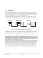
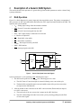
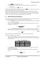
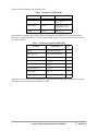
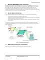
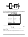
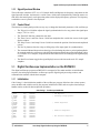
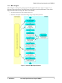
Interfacing a Data Acquisition System
to the DSP56303
Application Note
by
Mihai V. Micea
Vladimir Cretu
and Dan Chiciudean
AN2087/D
Rev. 0, 12/2000
This document contains information on a new product. Specifications and information herein are subject to change without notice.
Motorola reserves the right to make changes without further notice to any products herein. Motorola makes no warranty, representation or guarantee
regarding the suitability of its products for any particular purpose, nor does Motorola assume any liability arising out of the application or use of any product or
circuit, and specifically disclaims any and all liability, including without limitation consequential or incidental damages. “Typical” parameters which may be
provided in Motorola data sheets and/or specifications can and do vary in different applications and actual performance may vary over time. All operating
parameters, including “Typicals” must be validated for each customer application by customer’s technical experts. Motorola does not convey any license under
its patent rights nor the rights of others. Motorola products are not designed, intended, or authorized for use as components in systems intended for surgical
implant into the body, or other applications intended to support life, or for any other application in which the failure of the Motorola product could create a
situation where personal injury or death may occur. Should Buyer purchase or use Motorola products for any such unintended or unauthorized application,
Buyer shall indemnify and hold Motorola and its officers, employees, subsidiaries, affiliates, and distributors harmless against all claims, costs, damages, and
expenses, and reasonable attorney fees arising out of, directly or indirectly, any claim of personal injury or death associated with such unintended or
unauthorized use, even if such claim alleges that Motorola was negligent regarding the design or manufacture of the part.
Motorola and
are registered trademarks of Motorola, Inc. Motorola, Inc. is an Equal Opportunity/Affirmative Action Employer.
All other tradenames, trademarks, and registered trademarks are the property of their respective owners.
How to reach us:
USA/EUROPE/Locations Not Listed: Motorola Literature Distribution; P.O. Box 5405, Denver, Colorado, 80217
1-303-675-2140 or 1-800-441-2447
JAPAN: Motorola Japan, Ltd.; SPS, Technical Information Center, 3-20-1, Minami-Azabu, Minato-ku,
Tokyo 106-8573 Japan. 81-3-3440-3569
ASIA/PACIFIC: Motorola Semiconductors H.K. Ltd., Silicon Harbour Centre, 2 Dai King Street,
Tai Po Industrial Estate, Tai Po, N.T., Hong Kong. 852-26668334
Customer Focus Center: 1-800-521-6274
HOME PAGE: http://www.motorola.com/semiconductors
© Copyright Motorola, Inc., 2000
Abstract and Contents
This paper discusses the hardware and software aspects of interfacing a data acquisition system (DAQ) to
the DSP56303 digital signal processor. Included are descriptions of a generic DAQ system, a particular
DAQ system connected to the DSP56303, and a case study of this sytem that emulates the function of a
digital oscilloscope.
1
Introduction . . . . . . . . . . . . . . . . . . . . . . . . . . . . . . . . . . . . . . . . . . . . . . . . . . . . . . . . . . 1
2
Description of a Generic DAQ System . . . . . . . . . . . . . . . . . . . . . . . . . . . . . . . . . . 2
2.1
2.2
DAQ Operation. . . . . . . . . . . . . . . . . . . . . . . . . . . . . . . . . . . . . . . . . . . . . . . . . . . . . . . . . . 2
ADC Performance Parameters . . . . . . . . . . . . . . . . . . . . . . . . . . . . . . . . . . . . . . . . . . . . . . 3
3
Example DAQ-DSP System—Overview . . . . . . . . . . . . . . . . . . . . . . . . . . . . . . . . . 5
3.1
3.2
General System Architecture . . . . . . . . . . . . . . . . . . . . . . . . . . . . . . . . . . . . . . . . . . . . . . . 5
DAQ System Architecture and Operation . . . . . . . . . . . . . . . . . . . . . . . . . . . . . . . . . . . . . 5
4
Example DAQ-DSP System—Implementation Details . . . . . . . . . . . . . . . . . . . . 8
5
Case Study: Digital Oscilloscope Using the DSP56303 . . . . . . . . . . . . . . . . . . 12
5.1
5.2
5.2.1
5.2.2
5.2.3
5.3
5.3.1
5.3.2
5.3.3
5.4
General Features . . . . . . . . . . . . . . . . . . . . . . . . . . . . . . . . . . . . . . . . . . . . . . . . . . . . . . . . 12
Graphical User Interface . . . . . . . . . . . . . . . . . . . . . . . . . . . . . . . . . . . . . . . . . . . . . . . . . . 13
Signal Display Window . . . . . . . . . . . . . . . . . . . . . . . . . . . . . . . . . . . . . . . . . . . . . . . 14
Signal Spectrum Window . . . . . . . . . . . . . . . . . . . . . . . . . . . . . . . . . . . . . . . . . . . . . . 15
Control Panel . . . . . . . . . . . . . . . . . . . . . . . . . . . . . . . . . . . . . . . . . . . . . . . . . . . . . . . 15
Digital Oscilloscope Implementation on the DSP56303 . . . . . . . . . . . . . . . . . . . . . . . . . 15
Initialization . . . . . . . . . . . . . . . . . . . . . . . . . . . . . . . . . . . . . . . . . . . . . . . . . . . . . . . . 15
Main Program . . . . . . . . . . . . . . . . . . . . . . . . . . . . . . . . . . . . . . . . . . . . . . . . . . . . . . . 17
Oscilloscope Routines. . . . . . . . . . . . . . . . . . . . . . . . . . . . . . . . . . . . . . . . . . . . . . . . . 19
Communication with the Host Computer . . . . . . . . . . . . . . . . . . . . . . . . . . . . . . . . . . . . . 23
6
Conclusions . . . . . . . . . . . . . . . . . . . . . . . . . . . . . . . . . . . . . . . . . . . . . . . . . . . . . . . . . 24
7
About the Authors . . . . . . . . . . . . . . . . . . . . . . . . . . . . . . . . . . . . . . . . . . . . . . . . . . . 24
8
References . . . . . . . . . . . . . . . . . . . . . . . . . . . . . . . . . . . . . . . . . . . . . . . . . . . . . . . . . . 24
Abstract and Contents
iii
iv
Interfacing a Data Acquisition System to the DSP56303
1
Introduction
Digital data processing and control systems have become ubiquitous in modern daily life. Information
from a wide variety of environmental sources, including sound waves, light, temperature, gas pressure,
radiation, and mechanical movement, is converted to digital signals which are processed so that they can
communicate with intelligent user interface devices or embedded systems.
A typical approach for interfacing digital processing systems with the environment uses a modular
architecture shown in Figure 1. This figure shows a bidirectional flow of signals—the system can acquire
information from the outside (input) and can operate on the environment (output).
Analog Electrical Signals
Transducer Module
Figure 1.
Digital Signals
Signal
Conditioning
Signal
Conditioning
Non-electric Signals
DAQ Module
Digital Processing
System
General Architecture of a Digital Processing System Interface
The transducer module converts non-electric environmental input signals into analogous electric signals.
The data acquisition (DAQ) module contains one or more analog-to-digital converters (ADCs), which
sample the analog input signals and quantize the samples into binary coded (digital) signals. A
bidirectional system also contains at least one digital-to-analog converter (DAC) and a transducer that can
convert analog signals back to the corresponding environmental signals.
In most cases the electric signals generated by the transducers are not suitable for direct input to the ADC.
A signal conditioning block is required to adjust signal levels and impedance. This block can be included
in either the transducer or DAQ module. Many systems send the data processed by the DAQ-DSP system
to a host computer to provide an interactive user interface.
This paper discusses techniques for interfacing a unidirectional (input only) DAQ system to the DSP56303
digital signal processor. Both the hardware and software aspects of the interface are detailed. A generic
data acquisition system is described, followed by the details involved in connecting an example DAQ
system to the DSP56303. Finally, a case study is presented in which the example DAQ system and
DSP56303 are used to control a simple digital oscilloscope. In this case study a host computer, which
provides the display and control mechanisms (interactive user interface) of the oscilloscope, receives the
processed data from the DAQ system through an Extended Capability Port (ECP) standard interface.
Introduction
1
2
Description of a Generic DAQ System
This section describes the operation of a generic DAQ system and the parameters used to evaluate DAQ
system performance.
2.1
DAQ Operation
Figure 2 is a block diagram of a generic input-only data acquisition system. The primary components of
this system are an ADC and a data buffer that latches the ADC output and sends the data to the DSP. The
signals in this system include:
•
VIN—Analog input voltage from the transducer module
•
STC—Start of Conversion command to the ADC
•
EOC—End of Conversion signal from the ADC
•
Data—ADC output, binary-coded result of conversion
•
n—Number of output bits
•
WR—Data buffer write enable
•
RD—Data buffer read enable
•
RDDSP—Read signal issued by the DSP
•
DBus—DSP data bus
•
IRQ—Interrupt signal to the DSP.
RDDSP
STC
RD
VIN
Sampling
ADC
Data
n
DBus
Data
Buffer
WR
EOC
Figure 2.
IRQ
Generic DAQ System Connection Diagram
System operation is a cycle consisting of the following basic steps:
1. The DSP asserts (pulls low) the RDDSP line, which triggers two events:
a) The ADC Start of Conversion input is asserted, initiating a new conversion cycle.
b) The data buffer read enable input is asserted, and the results of the previous conversion
are output on the DSP data bus.
2. After an amount of time referred to as the ADC conversion time (Tconversion) has elapsed,
two ADC events occur:
a) The result code of the new conversion is output on the ADC data lines.
b) The ADC acknowledges the end of conversion cycle by asserting (pulling low) the End
of Conversion signal.
2
Interfacing a Data Acquisition System to the DSP56303
ADC Performance Parameters
3. Asserting EOC has the following two results:
a) The data buffer’s write enable signal is asserted, latching the new conversion result in
the data buffer.
b) The DSP interrupt signal (IRQ) is asserted.
The DSP interrupt handler responds to the interrupt by asserting RDDSP to read the conversion result and
initiate the next conversion (step 1), and the cycle repeats.
This is a simple, asynchronous system operating at maximum speed. It does not allow for variable
sampling/conversion rates and requires that the controlling DSP is fast enough to retrieve and store the
conversion results in one ADC cycle (Tconversion period). Therefore, this system can usually be found in
relatively low-to-medium speed data acquisition and digital processing products.
2.2
ADC Performance Parameters
The performance of a DAQ system in the frequency and amplitude domains is usually evaluated in terms
of a few simple ADC parameters. In the frequency domain, these parameters are:
•
Fs—The sampling rate is the number of times per second the analog input signal is sampled and
converted to digital representation.
•
Tconversion—The conversion time is the amount of time allotted per sample and is equal to the
reciprocal of the sampling rate:
Fs =
•
1
Tconversion
Eqn. 1
[Hz]
fmax in—The maximum input frequency that can be processed without aliasing. According to the
Nyquist Theorem of Sampling, this frequency must be less than half of the sampling frequency:
fmax in < Fs [Hz]
2
Eqn. 2
Thus, the sampling rate is the limiting parameter of the ADC in the frequency domain.
Parameters in the amplitude domain include:
•
FSR—The full scale range is the difference between the minimum and maximum current or
voltage allowed at the analog input lines. Typical values of full scale range for voltage-input ADCs
are listed in Table 1.
Table 1.
Typical Voltage FSR
FSR
Bipolar Input
Unipolar Input
20
-10 to +10
0 to 20
10
-5 to +5
0 to 10
5
-2.5 to +2.5
0 to 5
•
n—The number of bits in the encoded ADC conversion result. The larger n is, the better the
precision of the ADC output.
•
LSB—The least significant bit of the digital output indicates the resolution or granularity of
the ADC:
LSB =
FSR
[V or A]
2n
Description of a Generic DAQ System
Eqn. 3
3
Table 2 lists the parameters for a particular ADC.
Table 2.
Parameters for a Particular ADC
Parameter
Initial Specification
Derived Specifications
Sampling Rate
Fs = 100 kHz
Tconversion = 10 µs
fmaxIN < 50 kHz
Full Scale Range
FSR = 10 V
Bipolar input: –5 to +5V
Unipolar input: 0 to +10V
Resolution
n = 10 bits
LSB = 9.76 mV
One example of an actual ADC which is used on the DSP56303 and DSP56307 Evaluation Modules
(EVMs) is Crystal Semiconductor’s CS421x audio CODEC family. The specifications for these devices
are listed in Table 3.
Table 3.
Parameters for the CS421x CODEC Family
Parameter
Specifications
Unit
ADC type
Multimedia Audio CODEC
—
Operating principle
64x oversampling delta-sigma
—
Sampling rate
FS = 4 to 50
kHz
Conversion period
Tconversion = 250 to 20
µs
Maximum input frequency
fmaxIN < 2 to 25
kHz
Conversion resolution
n = 8 or 16
bit
Full scale range
FSR = 2.8
Vpp
Least significant bit (resolution)
LSB = 10.93 or 0.04
mV
These devices are suitable for audio applications. Applications requiring higher sampling rates or larger
input signal ranges require higher performance ADCs.
4
Interfacing a Data Acquisition System to the DSP56303
General System Architecture
3
Example DAQ-DSP System—Overview
This paper proposes a data acquisition and processing system based on the DSP56303 processor. The
analog signal acquisition and conversion operation is performed by a particular DAQ system under the
direct control of the DSP. Although the ADC in the DSP56303 Evaluation Module (the Crystal
Semiconductor’s CS4215 Multimedia Audio CODEC) is limited to the audio frequency range, the
principles illustrated here can be extended to provide a simple solution for data acquisition and processing
systems requiring higher performances than audio applications.
3.1
General System Architecture
A block diagram of the proposed system is shown in Figure 3. It features three main components:
•
A DAQ system, described in the remainder of this section.
•
A DSP56303-based board which controls overall system operation and performs all the digital data
processing needed for a particular application.
•
A host computer which functions as a graphical user interface and provides an interactive system
control platform.
The DAQ-DSP connection is described in detail in this paper. The DSP-host computer connection is
described in Motorola application note, ECP Standard Parallel Interface for DSP56300 Devices (order
number AN2085/D).
Figure 3.
3.2
Example System Block Diagram
DAQ System Architecture and Operation
Figure 4 on page 6 is a diagram of the DAQ employed in the proposed system.
Example DAQ-DSP System—Overview
5
RDDSP
R/C
EN
DB0–11
VN
12-Bit
Data
Buffer
ADS774
DBus
Status
Figure 4.
Example System DAQ Architecture
The Burr-Brown ADS774 was selected as the analog-to-digital component of the DAQ because of its
simple interface and command requirements as well as performance that is very well-suited to illustrate the
DAC—DSP interconnection described in Section 1. Table 4 lists the parameters of the ADS774. The
parameters in bold type are the ones selected for the example system.
Table 4.
ADS774 Main Parameters
Parameter
Specification
Unit
Operating principle
Successive approximation with
capacitor array
—
Conversion resolution
n = 12 or 8
bit
Minimum conversion time
Tconversion = 8 or 5.5
µs
Maximum sampling rate
FS = 117 or 125
kHz
Full scale range
Bipolar input voltage
Unipolar input voltage
Full scale range
Bipolar input voltage
Unipolar input voltage
FSR = 20
–10 to +10
0 to +20
FSR = 10
–5 to +5
0 to +10
V
Internal reference voltage
VREF = 2.5
V
Because the ADC is configured for 12-bit conversion resolution and 20-volt FSR, the resolution of the
system expressed in terms of the LSB is
LSB =
FSR
2n
=
20
2
12
= 4.88 mV
Eqn. 4
Two 74LS245-type octal bus transceivers, connected in parallel, serve as the 12-bit data buffer. These
devices were selected because they can shift the voltage level between the ADS774 5 V outputs and the
DSP56303 3.3 V inputs.
The DAQ system is configured to operate according to the timing diagram shown in Figure 5 and the
specifications in Figure 5 (source: Burr-Brown Corporation, Data Conversion Products, 1995).
6
Interfacing a Data Acquisition System to the DSP56303
DAQ System Architecture and Operation
tHRL
R/C
tDS
tConversion
Status
tHDR
DB11–DB0
tHS
High-Z State
Data Valid
Figure 5.
Data Valid
ADS774 Timing Diagram
Table 5. ADS774 Timing Specifications
Symbol
Parameter
Unit
Minimum
Maximum
tHRL
Low R/C pulse width
ns
25
—
tDS
Status delay from R/C
ns
—
200
Tconversion
Conversion time
µs
8
—
tHDR
Data valid after R/C low
ns
25
—
tHS
Status delay after data valid
ns
75
375
The ADS774 Status pin, which acknowledges the end of a conversion cycle, is not used in this system.
Instead, the timer interrupt routine on the DSP determines the desired conversion time, which is longer
than the Tconversion of the ADS774. This routine also initiates the conversion cycle and retrieves the data
result from the data buffer.
Example DAQ-DSP System—Overview
7
4
Example DAQ-DSP System—Implementation Details
The interface between the DSP56303 and the DAQ in the example system is shown in Figure 6. The
interface uses the DSP’s Port A lines as follows:
•
A Read signal, RD, simultaneously initiates a new conversion cycle on the DAQ and enables the
output of the DAQ data buffer to read the current conversion result.
•
DSP Data Bus lines 8–19 (DDB8–19) receive the 12-bit conversion result. (Lines DDB0–7 are used by
the DSP56303 Evaluation Module to transfer data from the on-board EEPROM.)
Figure 6.
Example System DAQ–DSP Connection
Figure 7 is a general timing diagram of the example system operation.
Figure 7.
Example System Timing Diagram
The falling edge of RD triggers a new conversion cycle on the ADC and simultaneously loads the ACQ
buffers with the previous conversion result.
The rising edge of RD strobes the buffered data to the DDB8–19 lines for storing into a predefined data
buffer in the DSP.
After a Tconversion delay, the result code of the current conversion cycle is available at the data output lines
of the ADC, ready to be buffered.
The full RD cycle period must be long enough to include the ADC conversion period (8 µs) plus a small
delay to allow for the data transfer from the buffer to the DSP. The RD period is about 9 µs in the example
system.
8
Interfacing a Data Acquisition System to the DSP56303
DAQ System Architecture and Operation
Data acquisition is fully controlled by DSP software. Code Example 1 provides a general framework for a
data acquisition and processing program on the DSP56303. This program initializes chip parameters (chip
clock and PLL, interrupts and Port A access), sets up a 512-word data buffer to store conversion result
codes, and initializes Timer0, which controls the overall data acquisition cycle by issuing a level 2
interrupt every 9 µs. Other user-defined routines can be added to process the acquired data when the buffer
is full.
Code Example 1. Data Acquisition and Processing Program on the DSP56303
I_RESET
M_PCTL
equ
equ
$000000
$FFFFFD
; Hardware RESET Vector.
; PLL Control Register.
M_IPRP
equ
$FFFFFE
; Interrupt Priority Register Peripheral
M_BCR
M_AAR1
equ
equ
$FFFFFB
$FFFFF8
; Bus Control Register.
; Address Attribute Register 1.
M_TCSR0
M_TLR0
M_TCPR0
I_TIM0C
equ
equ
equ
equ
$FFFF8F
$FFFF8E
$FFFF8D
$000024
;
;
;
;
BUFFER
BUFFLEN
BUFFULL
DAQ
equ
equ
equ
equ
$000000
511
$0007FF
$002000
; Data Buffer for conversion results.
; Length of data buffer.
; Flag set when the data buffer is full.
; DAQ address mapped on the external X memory
;; space.
Timer0
Timer0
Timer0
Timer0
Control/Status Register.
Load Register.
Compare Register.
Compare Interrupt Vector.
;
; Other variables can be defined here as required.
;
; Main program:
org
jmp
P:I_RESET
start
org
jsr
P:I_TIM0C
intr_t0
; Timer0 interrupt handler setup.
org
P:$100
; Start of the main program.
start
movep #$060003,X:M_PCTL
; Enable and set PLL: 16.934 MHz on-board clk
;; with MF=4. The resulting DSP internal clk =
;; 67.736 MHz.
movep #$11,X:M_AAR1
; Initialize Port A: external access type,
;; AAR1 pin positive polarity to avoid EEPROM
;; selection.
bset
bset
bset
bset
bset
#5,X:M_BCR
#6,X:M_BCR
#7,X:M_BCR
#8,X:M_BCR
#9,X:M_BCR
; Enable external X data space, number of wait
;; states = 31.
bset
bset
#8,X:M_IPRP
#9,X:M_IPRP
; Set Timer0 interrupt priority level to 2.
bclr
bclr
#9,sr
#8,sr
; Unmask all interrupts after RESET.
move
#BUFFER,R6
move
#0,BUFFULL
; Initialize the R6 register as current data
;; pointer in BUFFER.
; Initialize the flag used in the main
Example DAQ-DSP System—Implementation Details
9
Code Example 1 (Continued). Data Acquisition and Processing Program on the DSP56303
;; program to indicate that the data
;; data buffer is full.
movep #305,X:M_TCPR0
; Initialize Timer0 compare value so that
;; timer interrupt = 111.04 kHz
;; (timer period = 9.00 µsec).
movep #$302a05,X:M_TCSR0 ; Initialize Timer0 Control Register and start
;; timer.
;
; Other routines can be added here to process the data acquired in the
;; 512-word buffer that starts at X:$000000 address. BUFFULL flag
;; can be used to test if the buffer is available for processing.
;
Timer0 issues a level 2 interrupt every 9 µs to read a new conversion result into the DAQ data buffer and
simultaneously initiate a new ADC conversion cycle. The Timer0 interrupt handling routine in Code
Example 2 acquires data from the DAQ buffer through the Port A interface and writes the result into its
own data buffer, called BUFFER. The BUFFULL flag is used to alert the main program that the data buffer is
full and ready for further processing.
The Timer0 interrupt handler first checks BUFFER to see if it is full. If the buffer is full, the BUFFULL flag
is set and the handler terminates. If the buffer is not full, the interrupt handler reads another conversion
result code through the Port A DDB8-19 lines and stores it in the next location in the buffer, using the R6
register as a pointer. For reasons described later, the handler extracts the 8 most significant bits from each
12-bit conversion result; other applications can use the full 12-bit resolution for an improved data
processing precision.
Code Example 2. Timer0 Interrupt Handler
intr_t0
jset
#0,X:BUFFULL,intr_end
move
X:DAQ,B
extractu #$8024,B,A
intr_end
clr
clr
B A0,X:(R6)+
A
move
move
cmp
jgt
move
rti
#BUFLEN,A0
R6,B0
A,B
intr_end
#1,X:BUFFULL
; Test if the buffer is already full. If
;; so, exit the handler.
; Read the current conversion result into B
;; accumulator, and initiate a new conversion
;; cycle.
; Extract the 8 most significant bits from the
;; conversion result.
; Store current result into data buffer.
; If the data buffer pointer (R6) reaches the
;; end of buffer, set the BUFFULL flag.
; BUFFER is not full.
; Set BUFFULL flag.
The timer interrupt approach was selected for two important reasons:
1. This approach offers an easy and relatively exact timing solution, both for acquiring data
from the DAQ system and for commanding the conversion cycles, without requiring external
hardware such as timer or counters in the DAQ system to drive the sampling rate. The
acquisition period can easily be modified to accommodate the requirements of a particular
application by reprogramming the Timer0 Load Register (TLR0) to a new counting period.
2. DSP processing resources are freed up during the acquisition cycle and available for use by
other user-defined routines in the main program.
10
Interfacing a Data Acquisition System to the DSP56303
DAQ System Architecture and Operation
The data buffer in this program can be configured and used in several ways. One simple approach is to use
two data buffers—one for current acquisition and storing operations in the timer interrupt handler, and one
for data processing in the main program. When a buffer is filled, the interrupt handler sets the BUFFULL
flag to signal the main program that the buffer is ready for processing, and switches to the other buffer for
storing subsequent acquired data. The two buffers can be defined at the same base address, one in X
memory and one in Y memory.
Another approach is a circular buffer which allows access from the main program (read) and from the
interrupt handler (write).
Example DAQ-DSP System—Implementation Details
11
5
Case Study: Digital Oscilloscope Using the DSP56303
To illustrate the practical application of our example system, this section describes the design of a digital
oscilloscope using the DSP56303, with a host computer providing a graphical user interface and general
control panel.
5.1
General Features
The general architecture of the oscilloscope is based on the block diagram in Figure 3 on page 5. The
analog voltage input to the oscilloscope is applied to the DAQ system described in Section 3.2 on page
page 5, which features the Burr-Brown Analog ADS774 ADC. The digitized, buffered ADC output is
transferred to the DSP56303 via Port A.
The DSP performs all of the processing required to provide the functions which a typical oscilloscope
applies to a periodic input signal:
•
Signal synchronization
•
Minimum and maximum amplitude
•
Frequency and period
•
Fast Fourier Transform
A flexible and intuitive graphical user interface for the digital oscilloscope was designed using a host
computer. Data display windows, buttons, and slide bars provide a control panel that is easy to use. To
maximize throughput while maintaining system flexibility, the ECP standard parallel interface is used to
connect the DSP to the host computer.
Table 6 summarizes the main functional parameters of the digital oscilloscope.
Table 6.
Digital Oscilloscope Parameters
Parameter
Specification or Description
Analog Signal Interface
12
Input signal voltage range
–10 to +10 V
–5 to +5 V
0 to 10 V
0 to 20 V
Sampling rate
112K samples per second maximum.
Input signal frequency range
0 to 55.5 kHz
Input channels
1
Input impedance
12 kΩ (10 Vpp input)
50 kΩ (20 Vpp input)
Conversion resolution
12 bits
Least significant bit (LSB)
2.44 mV (10 Vpp input)
4.88 mV (20 Vpp input)
Interfacing a Data Acquisition System to the DSP56303
Graphical User Interface
Table 6.
Digital Oscilloscope Parameters (Continued)
Parameter
Specification or Description
Graphical User Interface
General features
Real–time graphical display of acquired signal
– time domain.
Real–time graphical display of acquired signal
– frequency domain.
Basic signal parameters calculation
– automatic or manual modes.
Signal display modes
RUN Mode—real-time display
FREEZE Mode—static display of a captured signal
Variable time base
256 stages ranging from 588 to 123,460 µs per division
Synchronization modes
Rising edge
Falling edge
Variable threshold in the –10 to +10 V range
Amplitude calculation
Automatic Mode: minimum and maximum amplitude values
displayed for 512 signal samples
Manual Mode: two mouse-controlled horizontal amplitude
cursors.
5.2
Frequency/period calculation
Two vertical time cursors moved with the mouse.
Oscilloscope calculates automatically the
corresponding time and frequency values.
Parameters calculated and
displayed continuously
Current time base in µs/DIV
Sampling frequency in Sps (Samples per second)
Synchronization threshold level in V
Instant values corresponding to the two horizontal
amplitude cursors in V.
Instant period and frequency values corresponding
to the two vertical time cursors, in seconds and Hz.
Signal frequency spectrum (FFT coefficients).
Instant frequency value corresponding to the
vertical cursor in the spectrogram, in Hz
Graphical User Interface
The graphical user interface emulates the display and control panel of an actual oscilloscope. It combines
the features of an analog oscilloscope with the advantages of digital processing:
•
Continuous calculation of signal parameters (amplitude, frequency, period)
•
Calculations performed either automatically or with the use of special, interactive,
mouse-controlled cursors
•
Facilities for changing the oscilloscope time base and synchronization modes
•
Memory capability
•
Real-time FFT calculation and graphic display of the corresponding frequency spectrum
The GUI program was developed under the LINUX platform using the SVGALib (Super VGA graphical
library) in console mode. Figure 8 on page 14 is a screen capture showing the GUI layout.
Case Study: Digital Oscilloscope Using the DSP56303
13
Figure 8.
Digital Oscilloscope Graphical User Interface
The oscilloscope GUI has separate windows for the signal, frequency spectrum, and control panel.
5.2.1 Signal Display Window
The signal display window displays the acquired signal in both real-time mode (RUN Mode) and as a static
image (FREEZE Mode). A grid is also displayed for better signal viewing.
Two sets of interactive cursors are available to calculate signal parameters—a pair of horizontal red
cursors for amplitude, and a pair of green vertical cursors for frequency/period. Each cursor can be placed
anywhere over the displayed signal using the mouse (the mouse pointer is colored in white) or with the
slide bars provided in the control panel.
A sliding arrow on the left side of the display grid indicates the current signal synchronization level, which
can be modified over the –10 V to +10 V range using the corresponding slide bar in the control panel.
The following parameters of the current signal and oscilloscope are displayed below the signal:
14
•
Synchronization level (V)
•
Sampling frequency (samples per second)
•
Time per division (µs)
•
Time period and frequency of vertical cursors (µs)
•
Amplitudes of lower and upper horizontal cursors (V)
Interfacing a Data Acquisition System to the DSP56303
Digital Oscilloscope Implementation on the DSP56303
5.2.2 Signal Spectrum Window
The oscilloscope calculates a FFT over a 512-sample buffer and displays the frequency components on the
signal spectrum window. An interactive vertical cursor, which can be manipulated by either the mouse or a
slide bar in the control panel, can be placed anywhere on the displayed frequency spectrum. The frequency
at which the cursor is placed is also displayed.
5.2.3 Control Panel
The interactive control panel provides an easy way to change the functional parameters of the oscilloscope.
•
•
•
•
•
•
•
5.3
The Trigger Level slide bar adjusts the signal synchronization level to any point in the signal input
range (–10 V to +10 V).
The Time/DIV slide bar controls the time base.
The Time Cursor 1 and Time Cursor 2 slide bars manipulate the vertical time cursors in the signal
display window.
The Ampl. Cursor 1 and Ampl. Cursor 2 slide bars control the position of the horizontal amplitude
cursors.
The Pos Trg button selects the rising or falling edge of the input signal for synchronization.
The Automatic/Manual button selects the trigger for calculating the point-to-point signal amplitude.
In automatic mode, the oscilloscope calculates the minimum and maximum signal amplitude values
over a buffer of 512 samples, and positions the horizontal cursors accordingly in the signal display
window.
The Run/Freeze button toggles the signal display between real-time mode and a 512-sample
snapshot.
Digital Oscilloscope Implementation on the DSP56303
The digital oscilloscope program on DSP56303 is composed of four main modules: an initialization
sequence, the main program module, oscilloscope-specific digital signal processing routines, and
communication routines with the host computer.
5.3.1 Initialization
Code Listing 1 is the initialization module of the oscilloscope program. It declares the various equates,
macro includes and variables used by the program, initializes the DSP, and sets up the timer interrupt
handler routine needed for data acquisition operations.
Code Listing 1. Oscilloscope Initialization
M_PCTL
I_RESET
I_TIM0C
M_IPRC
M_IPRP
M_TCSR0
M_TCPR0
M_TLR0
M_TCPR0
M_TCR0
M_HPCR
M_HDDR
M_HDR
M_BCR
M_AAR1
;
equ
equ
equ
equ
equ
equ
equ
equ
equ
equ
equ
equ
equ
equ
equ
$FFFFFD
$000000
$000024
$FFFFFF
$FFFFFE
$FFFF8F
$FFFF82
$FFFF8E
$FFFF8D
$FFFF8C
$FFFFC4
$FFFFC8
$FFFFC9
$FFFFFB
$FFFFF8
; PLL Register.
; Interrupt setup equates.
; Timer0 Registers.
; HI08 Port Registers.
; Bus Interface Registers.
Case Study: Digital Oscilloscope Using the DSP56303
15
Code Listing 1 (Continued). Oscilloscope Initialization
; Variables used in the program.
;
BUFFER
equ
$000000
BUFFLEN
equ
511
DAQ
equ
$002000
HOSTCLK
equ
PERIPHCLK
equ
PERIPHACK
equ
nACKREVERSE
equ
HOSTACK
equ
nREVERSEREQUEST equ
SAMPLE_RDY
equ
8
9
10
11
12
13
$7FF
TRIG_TYPE
SYNC_LEVEL
equ
equ
$7FE
$7FD
MAX_VAL
equ
$7FC
MIN_VAL
equ
$7FB
POINTS
equ
512
COEF
equ
$400
;
; Macros included for calculating the FFT.
;
include 'siggen’
include 'sincos'
include 'outdata'
include 'bitrev'
include 'fftr2a’
sincos POINTS,COEF
;
; P: memory space setup
;
org
P:I_RESET
jmp
Oscilloscope
org
P:I_TIM0C
jsr
Intr_T0
org
p:$100
Oscilloscope
movep #$060003,X:M_PCTL
move
bset
bset
bclr
bclr
movep
bset
bset
bset
bset
bset
movep
movep
bsr
#0,VBA
#8,X:M_IPRP
#9,X:M_IPRP
#9,SR
#8,SR
#$11,X:M_AAR1
#5,X:M_BCR
#6,X:M_BCR
#7,X:M_BCR
#8,X:M_BCR
#9,X:M_BCR
#0,X:M_TLR0
#$302a04,X:M_TCSR0
ECP_init
; Data buffer for acquired samples.
; DAQ System address mapped on the
;; external X: memory space.
; ECP communication variables
; Flag set by the timer interrupt
;; handler when a new conversion result
;; is ready to be read from DAQ.
; Parameter to set the trigger type.
; Sets the synchronization level for
;; signal acquisition.
; Stores the maximum sample value from
;; the data buffer.
; Stores the minimum sample value.
; Variables used by the ‘fftr2a’ macro.
; Initializes the sin-cos tables.
; Reset vector.
; Timer0 interrupt vector setup.
; Base of the Oscilloscope Program.
; Enable PLL: DSP internal clock
;; 67.736 MHz.
; Interrupts setup: Timer0 will have
;; the IPL=2.
; Port A initialization
; Enable external X data space, number
;; of wait states = 31.
; Timer0 setup sequence.
; Initialize the ECP data link to the
;; host.
;
; Timer0 interrupt handling routine. Sets the SAMPLE_RDY flag to inform the
;; acquisition routine (‘Acq_sample’) that a new conversion cycle can begin.
;
Intr_T0
bset
#0,X:SAMPLE_RDY
rti
16
Interfacing a Data Acquisition System to the DSP56303
Digital Oscilloscope Implementation on the DSP56303
5.3.2 Main Program
Code Listing 2 is a listing of the main program for the digital oscilloscope. Figure 9 on page 17 is a
flowchart of the main program. The jagged arrows in the figure represent asynchronous events, which
imply wait states on the receiving side. These events include:
•
ECP data transactions between DSP and the host.
•
DSP timer interrupts which acknowledge sample acquisition operations.
Figure 9.
Oscilloscope Main Program Flowchart
Case Study: Digital Oscilloscope Using the DSP56303
17
Code Listing 2. Oscilloscope Main Program
;
; Main program.
;
Main
move
#BUFFER,R0
jsr
jsr
ECP_init
Host_sync
jsr
move
ECP_read
A0,X:TRIG_TYPE
jsr
ECP_read
move A0,X:SYNC_LEVEL
jsr
ECP_read
clr
B
insert #$8008,A0,B
move B0,X:M_TCPR0
; Set R0 as the pointer to the
;; acquisition buffer.
; Initialize the ECP data link to host.
; Communication synchronization with
;; the host computer.
; Read first byte-wide parameter
;; from host: Signal
;; synchronization trigger type.
; Read the next parameter:
;; Signal synchronization level.
; Read the next parameter: Current
;; oscilloscope timebase value.
; Setup the counting period
;; for Timer0.
;
; Oscilloscope starts the input signal sampling and its specific processing
;; procedures.
;
jsr
Syncro
; Signal synchronization routine.
jsr
Acq_buffer
; Acquire a buffer of input samples.
jsr
Min_max
; Calculate the minimum and maximum
;; values of acquired samples
;; in BUFFLEN.
;
; Send the results of processing back to host computer.
move #BUFFER,R0
; Send the acquired data buffer.
do
#BUFFLEN,_send_buffer
move X:(R0)+,A0
bsr
ECP_write
_send_buffer
move
jsr
X:MAX_VAL,A0
ECP_write
; Send the maximum calculated value
;; over a buffer of acquired samples.
move
jsr
X:MIN_VAL,a0
ECP_write
; Send the minimum calculated value
;; over a buffer of acquired samples.
;
; Start the FFT calculation for a buffer of acquired input samples
;
clr
A
; Initialize a buffer in Y: memory
move #BUFFER,R0
;; corresponding to BUFFER
do
#BUFFLEN,_init_ybuf
;; for FFT algorithm.
move A0,Y:(R0)+
_init_ybuf
fftr2a POINTS,BUFFER,COEF
nop
bitrev POINTS,BUFFER
18
; Call the ‘fftr2a’ macro developed by
;; Motorola, Incorporated, to calculate
;; the FFT on DSP56300 family.
;; Macro inputs:
;; POINTS—number of FFT points;
;; BUFFER—start of input data buffers
;;
(normally ordered)
;; COEF—start of sine/cosine table.
;; Macro outputs: POINTS locations
;; (NOTE: Output data is bit-reversed.)
;; X:BUFFER—real values
;; Y:BUFFER—imaginary values
; Call the ‘bitrev’ macro developed by
;; Motorola, Incorporated, for the
Interfacing a Data Acquisition System to the DSP56303
Digital Oscilloscope Implementation on the DSP56303
Code Listing 2 (Continued). Oscilloscope Main Program
;; DSP56300 family, to unscramble the
;; results from ‘fft2ra’ macro.
;
; Send the results of FFT to host computer
;
move #BUFFER,R0
do
#BUFFLEN,_send_fft
; Base of the X: and Y: result buffers.
move X:(R0),A0
bsr
ECP_write
extract #$8008,A,A
bsr
ECP_write
; Send the real part of a coefficient.
move Y:(R0)+,A0
bsr
ECP_write
extract #$8008,A,A
bsr
ECP_write
; Send the imaginary part of a
;; coefficient.
_send_fft
;
; Loop back to acquire and process the next buffer of samples.
;
jmp
Main
5.3.3 Oscilloscope Routines
The main program calls specific routines to perform the basic oscilloscope functions. These functions, in
the order in which they are called, are:
1. Syncro—Synchronizes the input signal on the rising or falling edge at a specified voltage
level.
2. Acq_buffer—Buffers a set of input signal samples.
3. Min_max—Calculates the minimum and maximum values in the buffer.
4. fftr2a and bitrev—DSP56300 library routines developed by Motorola to perform
FFT calculations.
The Syncro and Acq_buffer routines also call the Acq_sample routine, which acquires a single input
signal sample.
5.3.3.1 Synchronizing the Oscilloscope to the Input Signal
The Syncro routine attempts to synchronize to the input signal using the following input parameters:
•
TRIG_TYPE—Determines whether synchronization occurs while the signal is rising or falling.
•
SYNC_LEVEL—The voltage level of the signal at which synchronization begins.
The synchronization procedure acquires input signal samples and ignores them until both of the following
conditions are met:
1. The signal is rising or falling according to the TRIG_TYPE parameter, and
2. The voltage level of the input signal is within a predefined tolerance of SYNC_LEVEL.
When these conditions are met, the routine exits successfully. If these conditions are not met before 2048
samples are acquired, it is assumed that the input signal is not periodic over 512 samples, which is the size
of the data buffer defined by the variable BUFFLEN, and the routine exits without synchronizing.
Figure 10 on page 20 illustrates the synchronization procedure on a periodic sine wave.
Case Study: Digital Oscilloscope Using the DSP56303
19
Syncro routine
activated
Syncro routine
exits successfully
SYNC_LEVEL
Samples acquired and ignored
Signal is synchronized
TRIG_TYPE = 0 (positive triggering)
Figure 10.
Signal Synchronization Procedure
The Syncro routine is given in Code Listing 3.
Code Listing 3. Signal Synchronization Routine (Syncro)
Syncro
move
#0,X0
move
jset
X:TRIG_TYPE,A0
#0,A0,_neg_value1
move
jsr
#0,X0
Pozitive
move
jsr
#0,X0
Negative
move
jsr
move
jclr
#0,X0
Pozitive
X:TRIG_TYPE,A0
#0,A0,_continue
move
jsr
#0,X0
Negative
; X0 is the sample counter used by the
;; ‘Counts’ routine, which forces
;; Syncro to abort when X0 = 2048
;; samples.
_poz_value1
_neg_value1
_poz_value2
_neg_value2
_continue
rts
Pozitive
; Acquire input samples and ignore them
;; as long as they are higher than the
;; synchronization level, SYNC_LEVEL.
jsr
jset
jsr
clr
move
dec
cmp
jgt
Counts
#0,B,_end_counts
Acq_sample
B
X:SYNC_LEVEL,B0
B
B,A
Pozitive
; See Code Listing 6 on page 23.
_end_pozitive
rts
20
Interfacing a Data Acquisition System to the DSP56303
Digital Oscilloscope Implementation on the DSP56303
Code Listing 3 (Continued). Signal Synchronization Routine (Syncro)
Negative
; Acquire input samples and ignore them
;; as long as they are lower than the
;; synchronization level, SYNC_LEVEL.
jsr
jset
jsr
clr
move
inc
cmp
jle
Counts
#0,B,_end_negative
Acq_sample
B
X:SYNC_LEVEL,B0
B
B,A
Negative
; See Code Listing 6 on page 23.
_end_negative
rts
Counts
; Increment sample counter X0.
;; If X0 = 2048, set bit 0 of
;; accumulator B as a flag to abort
;; Syncro routine.
clr
move
inc
nop
move
clr
move
cmp
jle
bset
A
X0,A0
A
A0,X0
B
#2048,B0
B,A
_end_counts
#0,B
_end_counts
rts
5.3.3.2 Buffering Acquired Input Data Samples
After the signal synchronization routine has been completed, the main program calls the
Acq_buffer routine to acquire BUFFLEN (512) samples and store them in a data buffer in X
memory starting at address BUFFER. This routine is listed in Code Listing 4.
Code Listing 4. Buffer Routine (Acq_buffer)
Acq_buffer
move
do
jsr
move
#BUFFER,R0
#BUFFLEN,_acq_buff
Acq_sample
A0,X:(R0)+
; See Code Listing 6 on page 23.
_acq_buff
rts
Case Study: Digital Oscilloscope Using the DSP56303
21
5.3.3.3 Calculating Minimum and Maximum Values
The Min_max routine listed in Code Listing 5 calculates the minimum and maximum sample values in the
data buffer starting at X address BUFFER. The results are stored in the variables MIN_VAL and MAX_VAL.
Code Listing 5. Minimum / Maximum Routine (Min_max)
Min_max
clr
nop
move
move
move
move
do
clr
move
clr
move
cmp
jle
move
A
A0,X:MAX_VAL
#$FF,A0
A0,X:MIN_VAL
#BUFFER,R0
#BUFFLEN,_minmax
A
X:(R0)+,A0
B
X:MAX_VAL,B0
B,A
_lower
A0,X:MAX_VAL
_lower
clr
nop
move
cmp
jgt
move
B
X:MIN_VAL,B0
B,A
_higher
A0,X:MIN_VAL
_higher
_minmax
rts
5.3.3.4 FFT Calculations
The main program calls the fftr2a and bitrev macros developed by Motorola to perform fast Fourier
calculations for devices in the DSP56300 family.
The fftr2a macro uses the following variables:
•
Inputs:
— POINTS—The number of FFT points (512 in this application).
— BUFFER—The base address of the data buffers (normally ordered) used by the macro in both
X and Y memory spaces.
— COEF—The base address of the sine/cosine table.
•
Outputs:
— X:BUFFER—The real values of the FFT results.
— Y:BUFFER—The imaginary values of the FFT results.
Because the output of the fftr2a macro is bit-reversed, the bitrev macro is called to unscramble the
data in BUFFER.
5.3.3.5 Acquiring a Single Data Sample
The Acq_sample routine listed in Code Listing 6 acquires a single input signal sample from the DAQ
system through the DSP56303 Port A peripheral. This second-level routine is called by the Syncro and
Acq_buffer routines.
22
Interfacing a Data Acquisition System to the DSP56303
Communication with the Host Computer
When Acq_sample is called, Timer0 is enabled to count down the time base delay. The program then
polls the SAMPLE_RDY flag until it is set by the interrupt handler which is called when Timer0 counts to
zero.The routine then reads the current conversion result from the DAQ and extracts the 8 least significant
bits. This is done to accommodate the other data processing routines, which all work with byte-wide data.
The 8-bit result is returned in the A0 accumulator.
Code Listing 6. Acquiring a Single Data Sample (Acq_sample)
Acq_sample
bclr
bset
#0,X:SAMPLE_RDY
#0,X:M_TCSR0
; Clear the acquisition flag.
; Start the timer to count down a
;; time base delay.
move
jclr
bclr
clr
move
X:SAMPLE_RDY,A0
#0,A0,_sample_wait
#0,X:M_TCSR0
A
X:DAQ,B
; Wait for the timer to issue an
;; interrupt and set the flag.
; Stop the timer.
_sample_wait
extractu #$8024,B,A
rts
5.4
; Read the conversion result from DAQ
;; into accumulator B and start
;; a new conversion cycle.
; Extract the 8 least significant bits.
Communication with the Host Computer
Because of the relatively high transfer rates needed to set the functional parameters of the oscilloscope on
the DSP and to communicate the results back to the host computer, the Extended Capabilities Port (ECP)
parallel interface standard is used as the communication between the DSP56303 and the host computer. A
more complete description of the implementation of this interface can be found in Motorola application
note, ECP Standard Parallel Interface for DSP56300 Devices (order number AN2085/D).
Case Study: Digital Oscilloscope Using the DSP56303
23
6
Conclusions
Digital signal processors such as the DSP56303 provide a convenient and efficient link between a data
acquisition (DAQ) system and the user interface provided by a host computer. The example system
described here illustrates the hardware and software considerations involved in implementing DAQ-DSP
communication. The principles illustrated here can be extended to higher-performance systems by
selecting an ADC with a faster sampling rate and extending the software algorithms to accommodate larger
data widths.
7
About the Authors
Mihai V. Micea is a lecturer at the Computer Software and Engineering Department at the Politehnica
University of Timisoara, and Executive Director of the DSP Applications Lab Timisoara (DALT)
sponsored by Digital DNA from Motorola.
Vladimir Cretu is a professor and Director of the Computer Software and Engineering Department at the
Politehnica University of Timisoara, and Director of the DSP Applications Lab Timisoara (DALT)
sponsored by Digital DNA from Motorola.
Dan Chiciudean is a student at the Automation and Computer Science Faculty at the Politehnica University
of Timisoara, and a member of the research and development team at DALT.
Contacts:
8
•
[email protected]
•
http://dsplabs.utt.ro/dalt/
References
DSP56000 24-bit Digital Signal Processor Family Manual (ordernumber DSP56KFAMUM/AD), Motorola,
1995.
DSP56300 24-bit Digital Signal Processor Family Manual(ordernumber DSP56300FM/D), Motorola,1997
DSP56303 User’s Manual (order number DSP56303UM/AD), Motorola, 1996.
DSP56303 Evaluation Module User’s Manual (ordernumber DSP56303EMUM/AD), Motorola, 1999.
Motorola DSP Assembler Reference Manual, Motorola, 1999.
Digital Signal Processing Principles, Algorithms and Applications, A J. G. Proakis and D. G. Manolakis,
3rd edition, Prentice-Hall, 1996.
Digital Signal Processing: A Practical Approach, E. C. Ifeachor, B. W. Jervis, Addison-Wesley
Publishing Company, 1993.
Burr-Brown IC Data Book, Data Conversion Products - 1995”, Burr-Brown Corporation, 1995.
ADS774, Microprocessor-Compatible Sampling CMOS Analog-to-Digital Converter, Product Data Sheet
1109F, Burr-Brown Corporation, 1995.
Coding Schemes Used with Data Converters, Jason Albanus, Application Note AN-175, Burr-Brown,
1991.
IEEE Standard Signaling Method for a Bidirectional Parallel Peripheral Interface for Personal
Computers, Draft D1.1, November 5, 1999, Institute of Electrical and Electronic Engineers, Inc.
Interfacing the PC. Interfacing the Extended Capabilities Port, Craig Peacock, February 28, 2000, Internet
Resource.
24
Interfacing a Data Acquisition System to the DSP56303