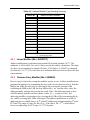
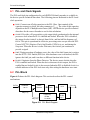
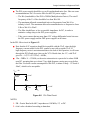
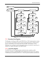
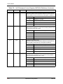
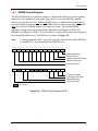
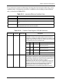
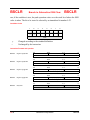
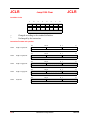
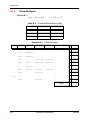
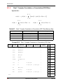
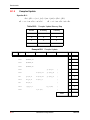
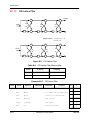
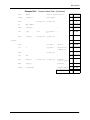
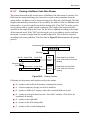
1
DSP56300 Family Manual 24-Bit Digital Signal Processor DSP56300FM/AD Revision 2.0, August 1999 OnCE and Mfax are trademarks of Motorola, Inc. Intel“ is a registered trademark of the Intel Corporation. All other trademarks are those of their respective owners. Motorola reserves the right to make changes without further notice to any products herein to improve reliability, function, or design. Motorola does not assume any liability arising out of the application or use of any product or circuit described herein; neither does it convey any license under its patent rights nor the rights of others. Motorola products are not authorized for use as components in life support devices or systems intended for surgical implant into the body or intended to support or sustain life. Buyer agrees to notify Motorola of any such intended end use whereupon Motorola shall determine availability and suitability of its product or products for the use intended. Motorola and are registered trademarks of Motorola, Inc. Motorola, Inc. is an Equal Employment Opportunity /Affirmative Action Employer. How to reach us: USA/Europe/Locations Not Listed: Motorola Literature Distribution P.O. Box 5405 Denver, Colorado 80217 1 (800) 441-2447 1 (303) 675-2140 Asia/Pacific: Motorola Semiconductors H.K. Ltd. 8B Tai Ping Industrial Park 51 Ting Kok Road Tai Po, N.T., Hong Kong 852-26629298 Japan: Nippon Motorola Ltd SPD, Strategic Planning Office141 4-32-1, Nishi-Gotanda Shinagawa-ku, Japan 81-3-5487-8488 Motorola Fax Back System (Mfax™): TOUCHTONE (602) 244-6609 1 (800) 774-1848 [email protected] Technical Resource Center: 1 (800) 521-6274 Internet: http://www.motorola-dsp.com/ DSP Helpline [email protected] MOTOROLA INC., 1999 Contents Chapter 1 Introduction 1.1 1.1.1 1.1.2 1.2 1.3 1.4 1.5 1.6 1.7 1.8 1.9 1.10 Core Overview. . . . . . . . . . . . . . . . . . . . . . . . . . . . . . . . . . . . . . . . . . . . . . . . . . . 1-2 Data Arithmetic Logic Unit (Data ALU) . . . . . . . . . . . . . . . . . . . . . . . . . . . . 1-2 Address Generation Unit (AGU) . . . . . . . . . . . . . . . . . . . . . . . . . . . . . . . . . . 1-3 Program Control Unit (PCU). . . . . . . . . . . . . . . . . . . . . . . . . . . . . . . . . . . . . . . . 1-4 On-chip Instruction Cache Controller . . . . . . . . . . . . . . . . . . . . . . . . . . . . . . . . . 1-5 Port A External Memory Interface . . . . . . . . . . . . . . . . . . . . . . . . . . . . . . . . . . . 1-6 Phase Lock Loop (PLL) and Clock Generator . . . . . . . . . . . . . . . . . . . . . . . . . . 1-6 Hardware Debugging Support . . . . . . . . . . . . . . . . . . . . . . . . . . . . . . . . . . . . . . . 1-7 Direct Memory Access (DMA) . . . . . . . . . . . . . . . . . . . . . . . . . . . . . . . . . . . . . . 1-7 Introduction to Digital Signal Processing . . . . . . . . . . . . . . . . . . . . . . . . . . . . . . 1-8 Summary of Features . . . . . . . . . . . . . . . . . . . . . . . . . . . . . . . . . . . . . . . . . . . . . 1-11 Manual Organization . . . . . . . . . . . . . . . . . . . . . . . . . . . . . . . . . . . . . . . . . . . . . 1-12 Chapter 2 Core Architecture Overview 2.1 Core Buses . . . . . . . . . . . . . . . . . . . . . . . . . . . . . . . . . . . . . . . . . . . . . . . . . . . . . . 2-2 2.2 Core Processing . . . . . . . . . . . . . . . . . . . . . . . . . . . . . . . . . . . . . . . . . . . . . . . . . . 2-3 2.3 Processing States . . . . . . . . . . . . . . . . . . . . . . . . . . . . . . . . . . . . . . . . . . . . . . . . . 2-5 2.3.1 Normal Processing State . . . . . . . . . . . . . . . . . . . . . . . . . . . . . . . . . . . . . . . . . 2-5 2.3.2 Exception Processing State (Interrupt Processing) . . . . . . . . . . . . . . . . . . . . . 2-6 2.3.2.1 Hardware Interrupt Source . . . . . . . . . . . . . . . . . . . . . . . . . . . . . . . . . . . . . . . 2-8 2.3.2.2 Software Interrupt Sources. . . . . . . . . . . . . . . . . . . . . . . . . . . . . . . . . . . . . . . 2-9 2.3.2.3 Interrupt Priority Structure . . . . . . . . . . . . . . . . . . . . . . . . . . . . . . . . . . . . . . . 2-9 2.3.2.4 Instructions Preceding the Interrupt Instruction Fetch. . . . . . . . . . . . . . . . . 2-12 2.3.2.5 Interrupt Types . . . . . . . . . . . . . . . . . . . . . . . . . . . . . . . . . . . . . . . . . . . . . . . 2-13 2.3.2.6 Interrupt Arbitration . . . . . . . . . . . . . . . . . . . . . . . . . . . . . . . . . . . . . . . . . . . 2-13 2.3.2.7 Interrupt Instruction Fetch . . . . . . . . . . . . . . . . . . . . . . . . . . . . . . . . . . . . . . 2-14 2.3.2.8 Interrupt Instruction Execution . . . . . . . . . . . . . . . . . . . . . . . . . . . . . . . . . . 2-14 2.3.3 Reset Processing State . . . . . . . . . . . . . . . . . . . . . . . . . . . . . . . . . . . . . . . . . 2-16 2.3.4 Wait Processing State . . . . . . . . . . . . . . . . . . . . . . . . . . . . . . . . . . . . . . . . . . 2-17 2.3.5 Stop Processing State . . . . . . . . . . . . . . . . . . . . . . . . . . . . . . . . . . . . . . . . . . 2-18 2.3.6 Debug State. . . . . . . . . . . . . . . . . . . . . . . . . . . . . . . . . . . . . . . . . . . . . . . . . . 2-18 Motorola Contents iii Chapter 3 Data Arithmetic Logic Unit 3.1 Introduction . . . . . . . . . . . . . . . . . . . . . . . . . . . . . . . . . . . . . . . . . . . . . . . . . . . . . 3-1 3.2 Data ALU Architecture . . . . . . . . . . . . . . . . . . . . . . . . . . . . . . . . . . . . . . . . . . . . 3-1 3.2.1 Data ALU Input Registers (X1, X0, Y1, Y0) . . . . . . . . . . . . . . . . . . . . . . . . . . . 3-3 3.2.2 Multiplier-Accumulator (MAC) Unit . . . . . . . . . . . . . . . . . . . . . . . . . . . . . . . . . 3-3 3.2.3 Data ALU Accumulator Registers (A2, A1, A0, B2, B1, B0) . . . . . . . . . . . . . . 3-4 3.2.4 Accumulator Shifter. . . . . . . . . . . . . . . . . . . . . . . . . . . . . . . . . . . . . . . . . . . . . . . 3-5 3.2.5 Bit Field Unit (BFU) . . . . . . . . . . . . . . . . . . . . . . . . . . . . . . . . . . . . . . . . . . . . . . 3-5 3.2.6 Data Shifter/Limiter. . . . . . . . . . . . . . . . . . . . . . . . . . . . . . . . . . . . . . . . . . . . . . . 3-5 3.2.6.1 Scaling . . . . . . . . . . . . . . . . . . . . . . . . . . . . . . . . . . . . . . . . . . . . . . . . . . . . . . 3-6 3.2.6.2 Limiting . . . . . . . . . . . . . . . . . . . . . . . . . . . . . . . . . . . . . . . . . . . . . . . . . . . . . 3-6 3.3 Data ALU Arithmetic and Rounding. . . . . . . . . . . . . . . . . . . . . . . . . . . . . . . . . . 3-7 3.3.1 Data Representation . . . . . . . . . . . . . . . . . . . . . . . . . . . . . . . . . . . . . . . . . . . . 3-7 3.3.2 Rounding Modes. . . . . . . . . . . . . . . . . . . . . . . . . . . . . . . . . . . . . . . . . . . . . . . 3-8 3.3.2.1 Convergent Rounding . . . . . . . . . . . . . . . . . . . . . . . . . . . . . . . . . . . . . . . . . . 3-8 3.3.2.2 Twos-Complement Rounding . . . . . . . . . . . . . . . . . . . . . . . . . . . . . . . . . . . 3-10 3.3.3 Arithmetic Saturation Mode . . . . . . . . . . . . . . . . . . . . . . . . . . . . . . . . . . . . . 3-11 3.3.4 Multiprecision Arithmetic Support. . . . . . . . . . . . . . . . . . . . . . . . . . . . . . . . 3-12 3.3.4.1 Double-Precision Multiply Mode . . . . . . . . . . . . . . . . . . . . . . . . . . . . . . . . 3-13 3.3.5 Block Floating-Point FFT Support . . . . . . . . . . . . . . . . . . . . . . . . . . . . . . . . 3-14 3.4 Data ALU Programming Model . . . . . . . . . . . . . . . . . . . . . . . . . . . . . . . . . . . . 3-15 3.5 Sixteen-Bit Arithmetic Mode . . . . . . . . . . . . . . . . . . . . . . . . . . . . . . . . . . . . . . 3-15 3.5.1 Moves in Sixteen-Bit Arithmetic Mode . . . . . . . . . . . . . . . . . . . . . . . . . . . . 3-16 3.5.1.1 Moves into Registers or Accumulators . . . . . . . . . . . . . . . . . . . . . . . . . . . . 3-16 3.5.1.2 Moves from Registers or Accumulators . . . . . . . . . . . . . . . . . . . . . . . . . . . 3-17 3.5.1.3 Short Immediate moves . . . . . . . . . . . . . . . . . . . . . . . . . . . . . . . . . . . . . . . . 3-19 3.5.1.4 Scaling and Limiting . . . . . . . . . . . . . . . . . . . . . . . . . . . . . . . . . . . . . . . . . . 3-19 3.5.2 Sixteen-bit Arithmetic. . . . . . . . . . . . . . . . . . . . . . . . . . . . . . . . . . . . . . . . . . 3-19 3.6 Pipeline Conflicts. . . . . . . . . . . . . . . . . . . . . . . . . . . . . . . . . . . . . . . . . . . . . . . . 3-20 3.6.1 Arithmetic Stall. . . . . . . . . . . . . . . . . . . . . . . . . . . . . . . . . . . . . . . . . . . . . . . 3-21 3.6.2 Status Stall . . . . . . . . . . . . . . . . . . . . . . . . . . . . . . . . . . . . . . . . . . . . . . . . . . 3-21 3.6.2.1 Transfer Stall. . . . . . . . . . . . . . . . . . . . . . . . . . . . . . . . . . . . . . . . . . . . . . . . . 3-22 Chapter 4 Address Generation Unit 4.1 4.2 4.3 AGU Architecture . . . . . . . . . . . . . . . . . . . . . . . . . . . . . . . . . . . . . . . . . . . . . . . . 4-1 Sixteen-bit Compatibility Mode . . . . . . . . . . . . . . . . . . . . . . . . . . . . . . . . . . . . . 4-3 Programming Model . . . . . . . . . . . . . . . . . . . . . . . . . . . . . . . . . . . . . . . . . . . . . . 4-4 Motorola DSP56300 Family Manual iv 4.3.1 Address Register Files . . . . . . . . . . . . . . . . . . . . . . . . . . . . . . . . . . . . . . . . . . 4-4 4.3.2 Stack Extension Pointer . . . . . . . . . . . . . . . . . . . . . . . . . . . . . . . . . . . . . . . . . 4-5 4.3.3 Offset Register Files . . . . . . . . . . . . . . . . . . . . . . . . . . . . . . . . . . . . . . . . . . . . 4-5 4.3.4 Modifier Register Files . . . . . . . . . . . . . . . . . . . . . . . . . . . . . . . . . . . . . . . . . 4-6 4.4 Addressing Modes . . . . . . . . . . . . . . . . . . . . . . . . . . . . . . . . . . . . . . . . . . . . . . . 4-6 4.4.1 Register Direct Modes . . . . . . . . . . . . . . . . . . . . . . . . . . . . . . . . . . . . . . . . . . 4-7 4.4.2 Address Register Indirect Modes . . . . . . . . . . . . . . . . . . . . . . . . . . . . . . . . . . 4-7 4.4.3 PC-relative Modes . . . . . . . . . . . . . . . . . . . . . . . . . . . . . . . . . . . . . . . . . . . . . 4-9 4.4.4 Special Address Modes. . . . . . . . . . . . . . . . . . . . . . . . . . . . . . . . . . . . . . . . . . 4-9 4.5 Address Modifier Types . . . . . . . . . . . . . . . . . . . . . . . . . . . . . . . . . . . . . . . . . . 4-10 4.5.1 Linear Modifier (Mn = $XXFFFF). . . . . . . . . . . . . . . . . . . . . . . . . . . . . . . . 4-11 4.5.2 Reverse-Carry Modifier (Mn = $000000) . . . . . . . . . . . . . . . . . . . . . . . . . . 4-11 4.5.3 Modulo Modifier (Mn = Modulus – 1). . . . . . . . . . . . . . . . . . . . . . . . . . . . . 4-12 4.5.4 Multiple Wrap-Around Modulo Modifier . . . . . . . . . . . . . . . . . . . . . . . . . . 4-13 Chapter 5 Program Control Unit 5.1 Overview . . . . . . . . . . . . . . . . . . . . . . . . . . . . . . . . . . . . . . . . . . . . . . . . . . . . . . . 5-1 5.2 PCU Hardware Architecture . . . . . . . . . . . . . . . . . . . . . . . . . . . . . . . . . . . . . . . . 5-3 5.3 Instruction Pipeline . . . . . . . . . . . . . . . . . . . . . . . . . . . . . . . . . . . . . . . . . . . . . . . 5-3 5.4 Programming Model . . . . . . . . . . . . . . . . . . . . . . . . . . . . . . . . . . . . . . . . . . . . . . 5-4 5.4.1 Configuration and Status Registers. . . . . . . . . . . . . . . . . . . . . . . . . . . . . . . . . 5-5 5.4.1.1 Operating Mode Register . . . . . . . . . . . . . . . . . . . . . . . . . . . . . . . . . . . . . . . . 5-6 5.4.1.2 Status Register (SR) . . . . . . . . . . . . . . . . . . . . . . . . . . . . . . . . . . . . . . . . . . . 5-11 5.4.2 Stack and Stack Extension . . . . . . . . . . . . . . . . . . . . . . . . . . . . . . . . . . . . . . 5-18 5.4.3 System Stack Configuration and Operation Registers . . . . . . . . . . . . . . . . . 5-18 5.4.3.1 Stack Pointer (SP) Register . . . . . . . . . . . . . . . . . . . . . . . . . . . . . . . . . . . . . 5-20 5.4.3.2 Stack Counter (SC) Register . . . . . . . . . . . . . . . . . . . . . . . . . . . . . . . . . . . . 5-22 5.4.3.3 Stack Size (SZ) Register . . . . . . . . . . . . . . . . . . . . . . . . . . . . . . . . . . . . . . . 5-22 5.4.4 Program, Loop, and Exception Processing Control . . . . . . . . . . . . . . . . . . . 5-23 5.4.4.1 Program Counter (PC) Register . . . . . . . . . . . . . . . . . . . . . . . . . . . . . . . . . . 5-23 5.4.4.2 Loop Address (LA) Register . . . . . . . . . . . . . . . . . . . . . . . . . . . . . . . . . . . . 5-23 5.4.4.3 Loop Counter (LC) Register . . . . . . . . . . . . . . . . . . . . . . . . . . . . . . . . . . . . 5-23 5.4.4.4 Vector Base Address (VBA) Register . . . . . . . . . . . . . . . . . . . . . . . . . . . . . 5-23 Chapter 6 PLL and Clock Generator 6.1 6.2 PLL and Clock Signals . . . . . . . . . . . . . . . . . . . . . . . . . . . . . . . . . . . . . . . . . . . . 6-2 PLL Block . . . . . . . . . . . . . . . . . . . . . . . . . . . . . . . . . . . . . . . . . . . . . . . . . . . . . . 6-2 Motorola Contents v 6.2.1 Frequency Predivider . . . . . . . . . . . . . . . . . . . . . . . . . . . . . . . . . . . . . . . . . . . 6-3 6.2.2 Phase Detector and Charge Pump Loop Filter . . . . . . . . . . . . . . . . . . . . . . . . 6-3 6.2.3 Voltage Controlled Oscillator (VCO). . . . . . . . . . . . . . . . . . . . . . . . . . . . . . . 6-3 6.2.3.1 Divide by 2 . . . . . . . . . . . . . . . . . . . . . . . . . . . . . . . . . . . . . . . . . . . . . . . . . . . 6-3 6.2.3.2 Frequency Divider . . . . . . . . . . . . . . . . . . . . . . . . . . . . . . . . . . . . . . . . . . . . . 6-3 6.2.3.3 PLL Control Elements . . . . . . . . . . . . . . . . . . . . . . . . . . . . . . . . . . . . . . . . . . 6-4 6.2.3.3.1 Clock Input Division . . . . . . . . . . . . . . . . . . . . . . . . . . . . . . . . . . . . . . . . 6-4 6.2.3.3.2 Frequency Multiplication . . . . . . . . . . . . . . . . . . . . . . . . . . . . . . . . . . . . . 6-4 6.2.3.3.3 Skew Elimination . . . . . . . . . . . . . . . . . . . . . . . . . . . . . . . . . . . . . . . . . . . 6-4 6.2.3.3.4 Clock Generator . . . . . . . . . . . . . . . . . . . . . . . . . . . . . . . . . . . . . . . . . . . . 6-5 6.2.3.3.5 Low-Power Divider (LPD) . . . . . . . . . . . . . . . . . . . . . . . . . . . . . . . . . . . . 6-5 6.2.3.3.6 Internal and External Clock Pulse Generator . . . . . . . . . . . . . . . . . . . . . . 6-5 6.2.3.3.7 Operating Frequency . . . . . . . . . . . . . . . . . . . . . . . . . . . . . . . . . . . . . . . . 6-6 6.3 PLL Programming Model . . . . . . . . . . . . . . . . . . . . . . . . . . . . . . . . . . . . . . . . . . 6-6 6.4 Clock Synchronization. . . . . . . . . . . . . . . . . . . . . . . . . . . . . . . . . . . . . . . . . . . . 6-10 6.5 Design Guidelines for Ripple and PCAP. . . . . . . . . . . . . . . . . . . . . . . . . . . . . . 6-10 Chapter 7 Debugging Support 7.1 JTAG Test Access Port . . . . . . . . . . . . . . . . . . . . . . . . . . . . . . . . . . . . . . . . . . . . 7-2 7.1.1 Boundary Scan Architecture Overview . . . . . . . . . . . . . . . . . . . . . . . . . . . . . 7-2 7.1.2 TAP Controller . . . . . . . . . . . . . . . . . . . . . . . . . . . . . . . . . . . . . . . . . . . . . . . . 7-3 7.1.3 Boundary Scan Register . . . . . . . . . . . . . . . . . . . . . . . . . . . . . . . . . . . . . . . . . 7-5 7.1.4 Instruction Register. . . . . . . . . . . . . . . . . . . . . . . . . . . . . . . . . . . . . . . . . . . . . 7-5 7.1.4.1 EXTEST (B[3 – 0] = 0000) . . . . . . . . . . . . . . . . . . . . . . . . . . . . . . . . . . . . . . 7-7 7.1.4.2 SAMPLE/PRELOAD (B[3 – 0] = 0001) . . . . . . . . . . . . . . . . . . . . . . . . . . . . 7-7 7.1.4.3 IDCODE (B[3 – 0] = 0010) . . . . . . . . . . . . . . . . . . . . . . . . . . . . . . . . . . . . . . 7-7 7.1.4.4 CLAMP (B[3 – 0] = 0011). . . . . . . . . . . . . . . . . . . . . . . . . . . . . . . . . . . . . . . 7-9 7.1.4.5 HI-Z (B[3 – 0] = 0100). . . . . . . . . . . . . . . . . . . . . . . . . . . . . . . . . . . . . . . . . . 7-9 7.1.4.6 ENABLE_ONCE(B[3:0] = 0110) . . . . . . . . . . . . . . . . . . . . . . . . . . . . . . . . . 7-9 7.1.4.7 DEBUG_REQUEST(B[3 – 0] = 0111) . . . . . . . . . . . . . . . . . . . . . . . . . . . . . 7-9 7.1.4.8 BYPASS (B[3 – 0] = 1111) . . . . . . . . . . . . . . . . . . . . . . . . . . . . . . . . . . . . . 7-10 7.1.5 DSP56300 JTAG Restrictions . . . . . . . . . . . . . . . . . . . . . . . . . . . . . . . . . . . 7-10 7.2 OnCE‘ Module. . . . . . . . . . . . . . . . . . . . . . . . . . . . . . . . . . . . . . . . . . . . . . . . . . 7-11 7.2.1 OnCE Controller . . . . . . . . . . . . . . . . . . . . . . . . . . . . . . . . . . . . . . . . . . . . . . 7-12 7.2.1.1 OnCE Command Register (OCR) . . . . . . . . . . . . . . . . . . . . . . . . . . . . . . . . 7-13 7.2.1.2 OnCE Decoder (ODEC). . . . . . . . . . . . . . . . . . . . . . . . . . . . . . . . . . . . . . . . 7-15 7.2.1.3 OnCE Status and Control Register (OSCR). . . . . . . . . . . . . . . . . . . . . . . . . 7-16 7.2.2 OnCE Memory Breakpoint Logic. . . . . . . . . . . . . . . . . . . . . . . . . . . . . . . . . 7-17 7.2.2.1 OnCE Memory Address Latch (OMAL) . . . . . . . . . . . . . . . . . . . . . . . . . . . 7-18 Motorola DSP56300 Family Manual vi 7.2.2.2 OnCE Memory Limit Register 0 (OMLR0). . . . . . . . . . . . . . . . . . . . . . . . . 7.2.2.3 OnCE Memory Address Comparator 0 (OMAC0) . . . . . . . . . . . . . . . . . . . 7.2.2.4 OnCE Memory Limit Register 1 (OMLR1). . . . . . . . . . . . . . . . . . . . . . . . . 7.2.2.5 OnCE Memory Address Comparator 1 (OMAC1) . . . . . . . . . . . . . . . . . . . 7.2.2.6 OnCE Breakpoint Control Register (OBCR) . . . . . . . . . . . . . . . . . . . . . . . . 7.2.2.7 OnCE Memory Breakpoint Counter (OMBC) . . . . . . . . . . . . . . . . . . . . . . . 7.2.3 Cache Support. . . . . . . . . . . . . . . . . . . . . . . . . . . . . . . . . . . . . . . . . . . . . . . . 7.2.3.1 OnCE Trace Logic . . . . . . . . . . . . . . . . . . . . . . . . . . . . . . . . . . . . . . . . . . . . 7.2.4 Methods of Entering Debug Mode . . . . . . . . . . . . . . . . . . . . . . . . . . . . . . . . 7.2.5 Trace Buffer . . . . . . . . . . . . . . . . . . . . . . . . . . . . . . . . . . . . . . . . . . . . . . . . . 7.2.6 OnCE Commands and Serial Protocol . . . . . . . . . . . . . . . . . . . . . . . . . . . . . 7.2.7 OnCE Module Examples . . . . . . . . . . . . . . . . . . . . . . . . . . . . . . . . . . . . . . . 7.2.7.1 Checking Whether the Chip Has Entered Debug Mode . . . . . . . . . . . . . . . 7.2.7.2 Polling the JTAG Instruction Register . . . . . . . . . . . . . . . . . . . . . . . . . . . . . 7.2.7.3 Saving Pipeline Information. . . . . . . . . . . . . . . . . . . . . . . . . . . . . . . . . . . . . 7.2.7.4 Reading the Trace Buffer . . . . . . . . . . . . . . . . . . . . . . . . . . . . . . . . . . . . . . . 7.2.7.5 Displaying a Specified Register . . . . . . . . . . . . . . . . . . . . . . . . . . . . . . . . . . 7.2.7.6 Displaying X Memory Area Starting at Address $xxxxxx . . . . . . . . . . . . . 7.2.7.7 Returning From Debug Mode to Normal Mode to Current Program . . . . . 7.2.7.8 Returning from Debug Mode to Normal Mode to a New Program . . . . . . . 7.3 Examples of JTAG-OnCE Interaction. . . . . . . . . . . . . . . . . . . . . . . . . . . . . . . . 7.3.1 Address Trace Mode . . . . . . . . . . . . . . . . . . . . . . . . . . . . . . . . . . . . . . . . . . . 7-18 7-18 7-19 7-19 7-19 7-21 7-21 7-22 7-23 7-26 7-27 7-29 7-29 7-29 7-29 7-30 7-31 7-31 7-32 7-32 7-33 7-36 Chapter 8 Instruction Cache 8.1 Instruction Cache Architecture . . . . . . . . . . . . . . . . . . . . . . . . . . . . . . . . . . . . . . 8.2 Cache Programming Model . . . . . . . . . . . . . . . . . . . . . . . . . . . . . . . . . . . . . . . . . 8.2.1 Cache Operation . . . . . . . . . . . . . . . . . . . . . . . . . . . . . . . . . . . . . . . . . . . . . . . 8.2.1.1 Program Fetch . . . . . . . . . . . . . . . . . . . . . . . . . . . . . . . . . . . . . . . . . . . . . . . . 8.2.1.2 Cache Hit . . . . . . . . . . . . . . . . . . . . . . . . . . . . . . . . . . . . . . . . . . . . . . . . . . . . 8.2.1.3 Cache Word Miss When Burst Mode Is Disabled . . . . . . . . . . . . . . . . . . . . . 8.2.1.4 Cache Word Miss When Burst Mode Is Enabled . . . . . . . . . . . . . . . . . . . . . 8.2.1.5 Sector Miss. . . . . . . . . . . . . . . . . . . . . . . . . . . . . . . . . . . . . . . . . . . . . . . . . . . 8.2.2 Default Mode After Hardware Reset . . . . . . . . . . . . . . . . . . . . . . . . . . . . . . . 8.3 Cache Locking . . . . . . . . . . . . . . . . . . . . . . . . . . . . . . . . . . . . . . . . . . . . . . . . . . . 8.4 Cache Unlocking . . . . . . . . . . . . . . . . . . . . . . . . . . . . . . . . . . . . . . . . . . . . . . . . . 8.5 Flushing the Cache. . . . . . . . . . . . . . . . . . . . . . . . . . . . . . . . . . . . . . . . . . . . . . . . 8.6 Data Transfers to/from Instruction Cache . . . . . . . . . . . . . . . . . . . . . . . . . . . . . . 8.6.1 DMA Transfers . . . . . . . . . . . . . . . . . . . . . . . . . . . . . . . . . . . . . . . . . . . . . . . . 8.6.2 Software-Controlled Transfers . . . . . . . . . . . . . . . . . . . . . . . . . . . . . . . . . . . . Motorola Contents 8-2 8-3 8-4 8-4 8-4 8-4 8-5 8-5 8-6 8-6 8-6 8-7 8-8 8-8 8-8 vii 8.7 8.8 Using the Instruction Cache in Real-Time Applications . . . . . . . . . . . . . . . . . . . 8-9 Debugging Instruction Cache Operation . . . . . . . . . . . . . . . . . . . . . . . . . . . . . . 8-10 Chapter 9 External Memory Interface (Port A) 9.1 Signal Description . . . . . . . . . . . . . . . . . . . . . . . . . . . . . . . . . . . . . . . . . . . . . . . . 9-2 9.2 Port Operation . . . . . . . . . . . . . . . . . . . . . . . . . . . . . . . . . . . . . . . . . . . . . . . . . . . 9-5 9.2.1 SRAM Support . . . . . . . . . . . . . . . . . . . . . . . . . . . . . . . . . . . . . . . . . . . . . . . . 9-5 9.2.2 DRAM Support. . . . . . . . . . . . . . . . . . . . . . . . . . . . . . . . . . . . . . . . . . . . . . . . 9-7 9.2.2.1 DRAM In-Page Access . . . . . . . . . . . . . . . . . . . . . . . . . . . . . . . . . . . . . . . . 9-10 9.2.2.2 DRAM Out-of-Page Access. . . . . . . . . . . . . . . . . . . . . . . . . . . . . . . . . . . . . 9-10 9.3 Port A Disable . . . . . . . . . . . . . . . . . . . . . . . . . . . . . . . . . . . . . . . . . . . . . . . . . . 9-11 9.4 Bus Handshake and Arbitration. . . . . . . . . . . . . . . . . . . . . . . . . . . . . . . . . . . . . 9-11 9.5 Bus Arbitration Signals . . . . . . . . . . . . . . . . . . . . . . . . . . . . . . . . . . . . . . . . . . . 9-11 9.5.1 The Arbitration Protocol. . . . . . . . . . . . . . . . . . . . . . . . . . . . . . . . . . . . . . . . 9-12 9.5.2 Arbitration Scheme . . . . . . . . . . . . . . . . . . . . . . . . . . . . . . . . . . . . . . . . . . . . 9-13 9.5.3 Bus Arbitration Example Cases . . . . . . . . . . . . . . . . . . . . . . . . . . . . . . . . . . 9-14 9.5.3.1 Case 1—Normal. . . . . . . . . . . . . . . . . . . . . . . . . . . . . . . . . . . . . . . . . . . . . . 9-14 9.5.3.2 Case 2—Bus Busy . . . . . . . . . . . . . . . . . . . . . . . . . . . . . . . . . . . . . . . . . . . . 9-14 9.5.3.3 Case 3—Low Priority . . . . . . . . . . . . . . . . . . . . . . . . . . . . . . . . . . . . . . . . . 9-14 9.5.3.4 Case 4—Default . . . . . . . . . . . . . . . . . . . . . . . . . . . . . . . . . . . . . . . . . . . . . . 9-14 9.5.3.5 Case 5—Bus Lock during Read-Modify-Write Instructions . . . . . . . . . . . . 9-14 9.5.3.6 Case 6—Bus Parking . . . . . . . . . . . . . . . . . . . . . . . . . . . . . . . . . . . . . . . . . . 9-15 9.6 Port A Control . . . . . . . . . . . . . . . . . . . . . . . . . . . . . . . . . . . . . . . . . . . . . . . . . . 9-15 9.6.1 Address Attribute Registers (AAR0–AAR3) . . . . . . . . . . . . . . . . . . . . . . . . 9-15 9.6.2 Bus Control Register. . . . . . . . . . . . . . . . . . . . . . . . . . . . . . . . . . . . . . . . . . . 9-18 9.6.3 DRAM Control Register. . . . . . . . . . . . . . . . . . . . . . . . . . . . . . . . . . . . . . . . 9-21 Chapter 10 DMA Controller 10.1 DMA Operational Overview . . . . . . . . . . . . . . . . . . . . . . . . . . . . . . . . . . . . . . . 10.1.1 Basic Address Modes . . . . . . . . . . . . . . . . . . . . . . . . . . . . . . . . . . . . . . . . . . 10.1.2 Special Address Modes. . . . . . . . . . . . . . . . . . . . . . . . . . . . . . . . . . . . . . . . . 10.1.3 Unmatched Source and Destination Dimensions . . . . . . . . . . . . . . . . . . . . . 10.1.4 DMA Triggers (Request Sources) . . . . . . . . . . . . . . . . . . . . . . . . . . . . . . . . 10.1.5 Transfer Mode. . . . . . . . . . . . . . . . . . . . . . . . . . . . . . . . . . . . . . . . . . . . . . . . 10.2 Timing (Core Clock Cycles) . . . . . . . . . . . . . . . . . . . . . . . . . . . . . . . . . . . . . . . 10.2.1 Non-Overlap Between DMA Channels . . . . . . . . . . . . . . . . . . . . . . . . . . . . 10.2.2 Overlap between DMA Channel and Core . . . . . . . . . . . . . . . . . . . . . . . . . . Motorola DSP56300 Family Manual 10-3 10-3 10-4 10-4 10-5 10-5 10-6 10-6 10-7 viii 10.3 Channel Priority. . . . . . . . . . . . . . . . . . . . . . . . . . . . . . . . . . . . . . . . . . . . . . . . . 10-7 10.3.1 Priority Between DMA Channels . . . . . . . . . . . . . . . . . . . . . . . . . . . . . . . . . 10-7 10.3.2 Priority Between a DMA Channel and the Core . . . . . . . . . . . . . . . . . . . . . 10-8 10.4 Special Uses of DMA With the Bus Interface Unit. . . . . . . . . . . . . . . . . . . . . . 10-9 10.4.1 Byte Packing . . . . . . . . . . . . . . . . . . . . . . . . . . . . . . . . . . . . . . . . . . . . . . . . . 10-9 10.4.1.1 DRAM In-Page Accesses using DMA. . . . . . . . . . . . . . . . . . . . . . . . . . . . . 10-9 10.4.1.2 End-of-Block-Transfer Interrupt . . . . . . . . . . . . . . . . . . . . . . . . . . . . . . . . . 10-9 10.5 DMA Controller Programming Model . . . . . . . . . . . . . . . . . . . . . . . . . . . . . . 10-10 10.5.1 DMA Source Address Registers (DSR0–DSR5) . . . . . . . . . . . . . . . . . . . . 10-10 10.5.2 DMA Destination Address Registers (DDR[5 – 0]) . . . . . . . . . . . . . . . . . . 10-11 10.5.3 DMA Counters (DCO[5 – 0]) . . . . . . . . . . . . . . . . . . . . . . . . . . . . . . . . . . . 10-11 10.5.3.1 DMA Counter Mode A—Single Counter . . . . . . . . . . . . . . . . . . . . . . . . . 10-11 10.5.3.2 DMA Counter Mode B—Dual Counter . . . . . . . . . . . . . . . . . . . . . . . . . . . 10-12 10.5.3.3 Circular Buffer (Length Less Than or Equal to 4K) . . . . . . . . . . . . . . . . . 10-13 10.5.3.3.1 DMA Counter Modes C, D and E—Triple Counter. . . . . . . . . . . . . . . 10-13 10.5.3.4 Circular Buffer (Length Greater Than 4K) . . . . . . . . . . . . . . . . . . . . . . . . 10-15 10.5.3.5 DMA Control Registers (DCR[5 – 0]). . . . . . . . . . . . . . . . . . . . . . . . . . . . 10-16 10.5.3.5.1 Non-3D Addressing Modes (D3D = 0) . . . . . . . . . . . . . . . . . . . . . . . . 10-21 10.5.3.5.2 3D Modes (D3D = 1) . . . . . . . . . . . . . . . . . . . . . . . . . . . . . . . . . . . . . . 10-22 10.5.3.6 DMA Offset Registers (DOR[3 – 0]). . . . . . . . . . . . . . . . . . . . . . . . . . . . . 10-24 10.5.3.7 DMA Status Register (DSTR) . . . . . . . . . . . . . . . . . . . . . . . . . . . . . . . . . . 10-24 10.6 DMA Restrictions . . . . . . . . . . . . . . . . . . . . . . . . . . . . . . . . . . . . . . . . . . . . . . 10-26 Chapter 11 Operating Modes and Memory Spaces 11.1 DSP56300 Family Core Memory Map . . . . . . . . . . . . . . . . . . . . . . . . . . . . . . . 11.1.1 X Data Memory Space . . . . . . . . . . . . . . . . . . . . . . . . . . . . . . . . . . . . . . . . . 11.1.2 Internal X I/O Space . . . . . . . . . . . . . . . . . . . . . . . . . . . . . . . . . . . . . . . . . . . 11.1.3 Switchable Internal or External X I/O Memory . . . . . . . . . . . . . . . . . . . . . . 11.1.3.1 Reserved Space for X ROM or RAM . . . . . . . . . . . . . . . . . . . . . . . . . . . . . 11.1.3.2 External X Data Memory . . . . . . . . . . . . . . . . . . . . . . . . . . . . . . . . . . . . . . . 11.1.3.3 Internal X Memory. . . . . . . . . . . . . . . . . . . . . . . . . . . . . . . . . . . . . . . . . . . . 11.1.4 Y Data Memory Space . . . . . . . . . . . . . . . . . . . . . . . . . . . . . . . . . . . . . . . . . 11.1.4.1 Internal/External Y I/O Space . . . . . . . . . . . . . . . . . . . . . . . . . . . . . . . . . . . 11.1.4.2 Switchable Internal or External Y I/O Memory. . . . . . . . . . . . . . . . . . . . . . 11.1.4.3 Reserved Space for Y ROM or RAM . . . . . . . . . . . . . . . . . . . . . . . . . . . . . 11.1.4.4 External Y Data Memory . . . . . . . . . . . . . . . . . . . . . . . . . . . . . . . . . . . . . . . 11.1.4.5 Internal Y Memory. . . . . . . . . . . . . . . . . . . . . . . . . . . . . . . . . . . . . . . . . . . . 11.1.5 Program Memory . . . . . . . . . . . . . . . . . . . . . . . . . . . . . . . . . . . . . . . . . . . . . 11.1.5.1 Bootstrap ROM Space . . . . . . . . . . . . . . . . . . . . . . . . . . . . . . . . . . . . . . . . . Motorola Contents 11-2 11-3 11-3 11-5 11-5 11-5 11-5 11-6 11-6 11-6 11-6 11-6 11-6 11-7 11-7 ix 11.1.5.2 Reserved Space for Program ROM . . . . . . . . . . . . . . . . . . . . . . . . . . . . . . . 11.1.5.3 External Program Memory. . . . . . . . . . . . . . . . . . . . . . . . . . . . . . . . . . . . . . 11.1.5.4 Internal Program Memory . . . . . . . . . . . . . . . . . . . . . . . . . . . . . . . . . . . . . . 11.1.5.5 Internal Instruction Cache RAM . . . . . . . . . . . . . . . . . . . . . . . . . . . . . . . . . 11.2 Sixteen-Bit Compatibility Mode . . . . . . . . . . . . . . . . . . . . . . . . . . . . . . . . . . . . 11.3 Memory Switch Mode . . . . . . . . . . . . . . . . . . . . . . . . . . . . . . . . . . . . . . . . . 11-7 11-7 11-7 11-8 11-8 11-9 Chapter 12 Guide to the Instruction Set 12.1 Instruction Formats and Syntax . . . . . . . . . . . . . . . . . . . . . . . . . . . . . . . . . . . . . 12-1 12.2 Operand Lengths . . . . . . . . . . . . . . . . . . . . . . . . . . . . . . . . . . . . . . . . . . . . . . . . 12-3 12.2.1 Data ALU Registers . . . . . . . . . . . . . . . . . . . . . . . . . . . . . . . . . . . . . . . . . . . 12-4 12.2.2 AGU Registers . . . . . . . . . . . . . . . . . . . . . . . . . . . . . . . . . . . . . . . . . . . . . . . 12-5 12.2.3 Program Control Registers . . . . . . . . . . . . . . . . . . . . . . . . . . . . . . . . . . . . . . 12-5 12.2.4 Data Organization in Memory . . . . . . . . . . . . . . . . . . . . . . . . . . . . . . . . . . . 12-6 12.3 Instruction Groups . . . . . . . . . . . . . . . . . . . . . . . . . . . . . . . . . . . . . . . . . . . . . . . 12-6 12.3.1 Arithmetic Instructions . . . . . . . . . . . . . . . . . . . . . . . . . . . . . . . . . . . . . . . . . 12-7 12.3.2 Logical Instructions . . . . . . . . . . . . . . . . . . . . . . . . . . . . . . . . . . . . . . . . . . . 12-9 12.3.3 Bit Manipulation Instructions . . . . . . . . . . . . . . . . . . . . . . . . . . . . . . . . . . . 12-10 12.3.4 Loop Instructions . . . . . . . . . . . . . . . . . . . . . . . . . . . . . . . . . . . . . . . . . . . . 12-11 12.3.5 Move Instructions . . . . . . . . . . . . . . . . . . . . . . . . . . . . . . . . . . . . . . . . . . . . 12-11 12.3.6 Program Control Instructions . . . . . . . . . . . . . . . . . . . . . . . . . . . . . . . . . . . 12-12 12.4 Guide to Instruction Descriptions . . . . . . . . . . . . . . . . . . . . . . . . . . . . . . . . . . 12-13 12.4.1 Notation . . . . . . . . . . . . . . . . . . . . . . . . . . . . . . . . . . . . . . . . . . . . . . . . . . . 12-14 12.4.2 Condition Code Computation . . . . . . . . . . . . . . . . . . . . . . . . . . . . . . . . . . . 12-18 12.5 Instruction Partial Encoding . . . . . . . . . . . . . . . . . . . . . . . . . . . . . . . . . . . . . . 12-22 12.5.1 Partial Encodings for Use in Instruction Encoding . . . . . . . . . . . . . . . . . . 12-22 12.5.2 Parallel Instruction Encoding of the Operation Code. . . . . . . . . . . . . . . . . 12-29 12.5.2.1 Multiply Instruction Encoding . . . . . . . . . . . . . . . . . . . . . . . . . . . . . . . . . . 12-29 12.5.2.2 Non-Multiply Instruction Encoding . . . . . . . . . . . . . . . . . . . . . . . . . . . . . . 12-30 Chapter 13 Instruction Set Appendix A Instruction Timing and Restrictions A.1 Overview . . . . . . . . . . . . . . . . . . . . . . . . . . . . . . . . . . . . . . . . . . . . . . . . . . . . . . A-1 A.2 Instruction Sequence Delays . . . . . . . . . . . . . . . . . . . . . . . . . . . . . . . . . . . . . . A-10 A.2.1 External Bus Wait States . . . . . . . . . . . . . . . . . . . . . . . . . . . . . . . . . . . . . . . A-10 Motorola DSP56300 Family Manual x A.2.2 Instruction Fetch Delays . . . . . . . . . . . . . . . . . . . . . . . . . . . . . . . . . . . . . . . . A-11 A.2.3 Data ALU Interlock . . . . . . . . . . . . . . . . . . . . . . . . . . . . . . . . . . . . . . . . . . . A-11 A.2.4 Address Register Interlocks . . . . . . . . . . . . . . . . . . . . . . . . . . . . . . . . . . . . . A-11 A.2.5 Stack Extension Delays . . . . . . . . . . . . . . . . . . . . . . . . . . . . . . . . . . . . . . . . A-13 A.2.6 Program Flow Control Delays . . . . . . . . . . . . . . . . . . . . . . . . . . . . . . . . . . . A-15 A.2.6.1 JMP to LA or to LA – 1 . . . . . . . . . . . . . . . . . . . . . . . . . . . . . . . . . . . . . . . . A-15 A.2.6.2 RTI to LA or to LA – 1 . . . . . . . . . . . . . . . . . . . . . . . . . . . . . . . . . . . . . . . . A-15 A.2.6.3 Conditional Instructions . . . . . . . . . . . . . . . . . . . . . . . . . . . . . . . . . . . . . . . . A-15 A.2.6.4 Interrupt Abort . . . . . . . . . . . . . . . . . . . . . . . . . . . . . . . . . . . . . . . . . . . . . . . A-16 A.2.6.5 Degenerated DO loop. . . . . . . . . . . . . . . . . . . . . . . . . . . . . . . . . . . . . . . . . . A-16 A.2.6.6 Annulled REP and DO . . . . . . . . . . . . . . . . . . . . . . . . . . . . . . . . . . . . . . . . . A-16 A.3 Instruction Sequence Restrictions . . . . . . . . . . . . . . . . . . . . . . . . . . . . . . . . . . A-16 A.3.1 Restrictions Near the End of DO Loops . . . . . . . . . . . . . . . . . . . . . . . . . . . . A-16 A.3.2 General DO Restrictions . . . . . . . . . . . . . . . . . . . . . . . . . . . . . . . . . . . . . . . . A-19 A.3.3 ENDDO Restrictions . . . . . . . . . . . . . . . . . . . . . . . . . . . . . . . . . . . . . . . . . . A-23 A.3.4 BRKcc Restrictions. . . . . . . . . . . . . . . . . . . . . . . . . . . . . . . . . . . . . . . . . . . . A-23 A.3.5 RTI and RTS Restrictions. . . . . . . . . . . . . . . . . . . . . . . . . . . . . . . . . . . . . . . A-24 A.3.6 SR Manipulation Restrictions . . . . . . . . . . . . . . . . . . . . . . . . . . . . . . . . . . . . A-24 A.3.7 SP/SC and SSH/SSL Manipulation Restrictions . . . . . . . . . . . . . . . . . . . . . A-24 A.3.8 Fast Interrupt Routines . . . . . . . . . . . . . . . . . . . . . . . . . . . . . . . . . . . . . . . . . A-25 A.3.9 REP Restrictions . . . . . . . . . . . . . . . . . . . . . . . . . . . . . . . . . . . . . . . . . . . . . . A-25 A.3.10 Stack Extension Restrictions . . . . . . . . . . . . . . . . . . . . . . . . . . . . . . . . . . . . A-26 A.3.11 Stack Extension Enable Restrictions . . . . . . . . . . . . . . . . . . . . . . . . . . . . . . A-26 A.4 Peripheral Pipeline Restrictions. . . . . . . . . . . . . . . . . . . . . . . . . . . . . . . . . . . . A-27 A.4.1 Polling a Peripheral Device for Write. . . . . . . . . . . . . . . . . . . . . . . . . . . . . . A-27 A.4.2 Writing to a Read-Only Register . . . . . . . . . . . . . . . . . . . . . . . . . . . . . . . . . A-28 A.4.3 XY Memory Data Move . . . . . . . . . . . . . . . . . . . . . . . . . . . . . . . . . . . . . . . . A-28 A.5 Sixteen-Bit Compatibility Mode Restrictions . . . . . . . . . . . . . . . . . . . . . . . . . A-28 Appendix B Benchmark Programs B.1 Benchmarks . . . . . . . . . . . . . . . . . . . . . . . . . . . . . . . . . . . . . . . . . . . . . . . . . . . . . B-2 B.1.1 Real Multiply . . . . . . . . . . . . . . . . . . . . . . . . . . . . . . . . . . . . . . . . . . . . . . . . . B-3 B.1.2 N Real Multiplies . . . . . . . . . . . . . . . . . . . . . . . . . . . . . . . . . . . . . . . . . . . . . . B-4 B.1.3 Real Update. . . . . . . . . . . . . . . . . . . . . . . . . . . . . . . . . . . . . . . . . . . . . . . . . . . B-5 B.1.4 N Real Updates . . . . . . . . . . . . . . . . . . . . . . . . . . . . . . . . . . . . . . . . . . . . . . . . B-6 B.1.5 Real Correlation or Convolution (FIR Filter) . . . . . . . . . . . . . . . . . . . . . . . . . B-7 B.1.6 Real * Complex Correlation or Convolution (FIR Filter) . . . . . . . . . . . . . . . B-8 B.1.7 Complex Multiply. . . . . . . . . . . . . . . . . . . . . . . . . . . . . . . . . . . . . . . . . . . . . B-10 B.1.8 N Complex Multiplies . . . . . . . . . . . . . . . . . . . . . . . . . . . . . . . . . . . . . . . . . B-11 Motorola Contents xi B.1.9 B.1.10 B.1.11 B.1.12 B.1.13 B.1.14 B.1.15 B.1.16 B.1.17 B.1.18 B.1.19 B.1.20 B.1.21 B.1.22 B.1.23 B.1.24 B.1.25 B.1.26 B.1.27 Complex Update . . . . . . . . . . . . . . . . . . . . . . . . . . . . . . . . . . . . . . . . . . . . . . B-12 N Complex Updates . . . . . . . . . . . . . . . . . . . . . . . . . . . . . . . . . . . . . . . . . . . B-13 Complex Correlation or Convolution (FIR Filter) . . . . . . . . . . . . . . . . . . . . B-15 Nth Order Power Series (Real) . . . . . . . . . . . . . . . . . . . . . . . . . . . . . . . . . . . B-17 Second Order Real Biquad IIR Filter . . . . . . . . . . . . . . . . . . . . . . . . . . . . . . B-18 N Cascaded Real Biquad IIR Filter . . . . . . . . . . . . . . . . . . . . . . . . . . . . . . . B-19 N Radix-2 FFT Butterflies (DIT, In-Place Algorithm). . . . . . . . . . . . . . . . . B-20 True (Exact) LMS Adaptive Filter . . . . . . . . . . . . . . . . . . . . . . . . . . . . . . . . B-21 Delayed LMS Adaptive Filter. . . . . . . . . . . . . . . . . . . . . . . . . . . . . . . . . . . . B-24 FIR Lattice Filter . . . . . . . . . . . . . . . . . . . . . . . . . . . . . . . . . . . . . . . . . . . . . B-26 All Pole IIR Lattice Filter . . . . . . . . . . . . . . . . . . . . . . . . . . . . . . . . . . . . . . . B-28 General Lattice Filter . . . . . . . . . . . . . . . . . . . . . . . . . . . . . . . . . . . . . . . . . . B-30 Normalized Lattice Filter . . . . . . . . . . . . . . . . . . . . . . . . . . . . . . . . . . . . . . . B-32 [1 × 3][3 × 3] Matrix Multiplication . . . . . . . . . . . . . . . . . . . . . . . . . . . . . . . B-34 N Point 3 × 3 2-D FIR Convolution . . . . . . . . . . . . . . . . . . . . . . . . . . . . . . . B-35 Viterbi Add-Compare-Select (ACS). . . . . . . . . . . . . . . . . . . . . . . . . . . . . . . B-38 Parsing a Data Stream. . . . . . . . . . . . . . . . . . . . . . . . . . . . . . . . . . . . . . . . . . B-41 Creating a Data Stream . . . . . . . . . . . . . . . . . . . . . . . . . . . . . . . . . . . . . . . . . B-42 Parsing a Hoffman Code Data Stream . . . . . . . . . . . . . . . . . . . . . . . . . . . . . B-45 Appendix C From CDR Process to HiP Process C.1 C.2 C.3 C.4 Voltage. . . . . . . . . . . . . . . . . . . . . . . . . . . . . . . . . . . . . . . . . . . . . . . . . . . . . . . . . C-2 Operating Frequency . . . . . . . . . . . . . . . . . . . . . . . . . . . . . . . . . . . . . . . . . . . . . . C-2 Port A Timings . . . . . . . . . . . . . . . . . . . . . . . . . . . . . . . . . . . . . . . . . . . . . . . . . . C-2 Memory Block Size . . . . . . . . . . . . . . . . . . . . . . . . . . . . . . . . . . . . . . . . . . . . . . . C-3 Motorola DSP56300 Family Manual xii Figures Figure 1-1. Figure 1-2. Figure 1-3. Figure 1-4. Figure 2-1. Figure 2-1. Figure 2-2. Figure 3-1. Figure 3-2. Figure 3-3. Figure 3-4. Figure 3-5. Figure 3-6. Figure 3-7. Figure 3-8. Figure 3-9. Figure 3-10. Figure 3-11. Figure 3-12. Figure 3-13. Figure 4-1 Figure 4-2 Figure 5-1. Figure 5-2. Figure 5-3. Figure 5-4. Figure 5-5. Figure 5-6. Figure 6-1. Figure 6-2. Figure 6-3. Figure 6-4. Figure 6-5. Figure 7-1. Motorola DSP56300 Family-Based DSP Chip . . . . . . . . . . . . . . . . . . . . . . . . . . . . . . . . . . 1-1 Analog Signal Processing . . . . . . . . . . . . . . . . . . . . . . . . . . . . . . . . . . . . . . . . . . 1-8 Digital Signal Processing . . . . . . . . . . . . . . . . . . . . . . . . . . . . . . . . . . . . . . . . . . 1-9 Mapping DSP Algorithms into Hardware . . . . . . . . . . . . . . . . . . . . . . . . . . . . . 1-11 DSP56303 Block Diagram . . . . . . . . . . . . . . . . . . . . . . . . . . . . . . . . . . . . . . . . . 2-3 Interrupt Priority Register C (IPRC) . . . . . . . . . . . . . . . . . . . . . . . . . . . . . . . . . 2-10 Interrupt Priority Register P (IPRP) . . . . . . . . . . . . . . . . . . . . . . . . . . . . . . . . . 2-11 Data ALU Block Diagram. . . . . . . . . . . . . . . . . . . . . . . . . . . . . . . . . . . . . . . . . . 3-2 Bit Weighting and Alignment of Operands. . . . . . . . . . . . . . . . . . . . . . . . . . . . . 3-7 Integer/Fractional Multiplication . . . . . . . . . . . . . . . . . . . . . . . . . . . . . . . . . . . . 3-8 Convergent Rounding (No Scaling) . . . . . . . . . . . . . . . . . . . . . . . . . . . . . . . . . . 3-9 Twos Complement Rounding (No Scaling) . . . . . . . . . . . . . . . . . . . . . . . . . . . 3-10 DMAC Implementation. . . . . . . . . . . . . . . . . . . . . . . . . . . . . . . . . . . . . . . . . . . 3-12 Double-Precision Multiplication Using DMAC . . . . . . . . . . . . . . . . . . . . . . . . 3-13 Double-Precision Algorithm . . . . . . . . . . . . . . . . . . . . . . . . . . . . . . . . . . . . . . . 3-14 Data ALU Core Programming Model . . . . . . . . . . . . . . . . . . . . . . . . . . . . . . . . 3-15 Sixteen-Bit Arithmetic Mode Data Organization . . . . . . . . . . . . . . . . . . . . . . . 3-16 Pipeline Conflicts—Arithmetic Stall. . . . . . . . . . . . . . . . . . . . . . . . . . . . . . . . . 3-21 Pipeline Conflicts—Status Stall . . . . . . . . . . . . . . . . . . . . . . . . . . . . . . . . . . . . 3-22 Pipeline Conflicts—Transfer Stall . . . . . . . . . . . . . . . . . . . . . . . . . . . . . . . . . . 3-23 AGU Block Diagram. . . . . . . . . . . . . . . . . . . . . . . . . . . . . . . . . . . . . . . . . . . . . . 4-2 AGU Programming Model . . . . . . . . . . . . . . . . . . . . . . . . . . . . . . . . . . . . . . . . . 4-4 PCU Architecture . . . . . . . . . . . . . . . . . . . . . . . . . . . . . . . . . . . . . . . . . . . . . . . . 5-3 Seven-Stage Pipeline. . . . . . . . . . . . . . . . . . . . . . . . . . . . . . . . . . . . . . . . . . . . . . 5-4 PCU Programming Model. . . . . . . . . . . . . . . . . . . . . . . . . . . . . . . . . . . . . . . . . . 5-5 Operating Mode Register (OMR) . . . . . . . . . . . . . . . . . . . . . . . . . . . . . . . . . . . . 5-7 Status Register (SR) . . . . . . . . . . . . . . . . . . . . . . . . . . . . . . . . . . . . . . . . . . . . . 5-12 Stack Pointer (SP) Register Format. . . . . . . . . . . . . . . . . . . . . . . . . . . . . . . . . . 5-20 PLL Clock Generator Block Diagram. . . . . . . . . . . . . . . . . . . . . . . . . . . . . . . . . 6-1 PLL Block Diagram . . . . . . . . . . . . . . . . . . . . . . . . . . . . . . . . . . . . . . . . . . . . . . 6-2 CLKGEN Block Diagram . . . . . . . . . . . . . . . . . . . . . . . . . . . . . . . . . . . . . . . . . . 6-5 PLL Control Register (PCTL). . . . . . . . . . . . . . . . . . . . . . . . . . . . . . . . . . . . . . . 6-6 PLL Filter Circuit . . . . . . . . . . . . . . . . . . . . . . . . . . . . . . . . . . . . . . . . . . . . . . . 6-11 Test Access Port with OnCE Module Block Diagram . . . . . . . . . . . . . . . . . . . . 7-4 DSP56300 Family Manual xiii Figure 7-2. Figure 7-3. Figure 7-3. Figure 7-4. Figure 7-6. Figure 7-5. Figure 7-7. Figure 7-8. Figure 7-9. Figure 7-10. Figure 7-11. Figure 7-12. Figure 7-13. Figure 7-14. Figure 7-15. Figure 8-1. Figure 9-1. Figure 9-2. Figure 9-3. Figure 9-4. Figure 9-5. Figure 9-6. Figure 9-7. Figure 9-8. Figure 9-9. Figure 10-1. Figure 10-2. Figure 10-3. Figure 10-4. Figure 10-5. Figure 10-6. Figure 11-1. Figure 11-2. Figure 12-1. Figure 12-2. Figure 12-3. Figure 12-4. Figure 12-5. Motorola TAP Controller State Machine . . . . . . . . . . . . . . . . . . . . . . . . . . . . . . . . . . . . . . 7-5 JTAG Instruction Register Format . . . . . . . . . . . . . . . . . . . . . . . . . . . . . . . . . . . 7-6 Identification Register Configuration . . . . . . . . . . . . . . . . . . . . . . . . . . . . . . . . . 7-7 Bypass Register . . . . . . . . . . . . . . . . . . . . . . . . . . . . . . . . . . . . . . . . . . . . . . . . . 7-10 OnCE Multiprocessor Configuration . . . . . . . . . . . . . . . . . . . . . . . . . . . . . . . . 7-12 OnCE Block Diagram . . . . . . . . . . . . . . . . . . . . . . . . . . . . . . . . . . . . . . . . . . . . 7-12 OnCE Controller . . . . . . . . . . . . . . . . . . . . . . . . . . . . . . . . . . . . . . . . . . . . . . . . 7-13 OnCE Command Register (OCR) Format . . . . . . . . . . . . . . . . . . . . . . . . . . . . 7-13 OnCE Status and Control Register (OSCR) . . . . . . . . . . . . . . . . . . . . . . . . . . . 7-16 OnCE Memory Breakpoint Logic 0 . . . . . . . . . . . . . . . . . . . . . . . . . . . . . . . . . 7-18 OnCE Breakpoint Control Register (OBCR) . . . . . . . . . . . . . . . . . . . . . . . . . . 7-19 Circular Tags Buffer (TAGB) . . . . . . . . . . . . . . . . . . . . . . . . . . . . . . . . . . . . . . 7-22 OnCE Trace Logic Block Diagram . . . . . . . . . . . . . . . . . . . . . . . . . . . . . . . . . . 7-23 OnCE Pipeline Information and GDB Registers. . . . . . . . . . . . . . . . . . . . . . . . 7-25 OnCE Trace Buffer Block Diagram . . . . . . . . . . . . . . . . . . . . . . . . . . . . . . . . . 7-28 Instruction Cache Block Diagram . . . . . . . . . . . . . . . . . . . . . . . . . . . . . . . . . . . . 8-3 SRAM Access with One Wait State Example . . . . . . . . . . . . . . . . . . . . . . . . . . 9-6 Example SRAM Connection Diagram . . . . . . . . . . . . . . . . . . . . . . . . . . . . . . . . 9-7 DRAM Read Access (In-Page) with Two Wait States . . . . . . . . . . . . . . . . . . . . 9-9 DRAM Write Access (In-Page) with Two Wait States Example . . . . . . . . . . . . 9-9 Typical DRAM Connection Diagram . . . . . . . . . . . . . . . . . . . . . . . . . . . . . . . . 9-10 Example Bus Arbitration Scheme . . . . . . . . . . . . . . . . . . . . . . . . . . . . . . . . . . . 9-13 Address Attribute Registers (AAR0–AAR3) . . . . . . . . . . . . . . . . . . . . . . . . . . 9-16 Bus Control Register (BCR) . . . . . . . . . . . . . . . . . . . . . . . . . . . . . . . . . . . . . . . 9-19 DRAM Control Register (DCR) . . . . . . . . . . . . . . . . . . . . . . . . . . . . . . . . . . . . 9-21 DMA Controller Programming Model . . . . . . . . . . . . . . . . . . . . . . . . . . . . . . 10-10 DMA Counter Mode A Layout . . . . . . . . . . . . . . . . . . . . . . . . . . . . . . . . . . . . 10-11 DMA Counter Mode B Layout . . . . . . . . . . . . . . . . . . . . . . . . . . . . . . . . . . . . 10-12 DMA Counter Modes C, D, and E Layouts . . . . . . . . . . . . . . . . . . . . . . . . . . 10-14 DMA Control Register (DCR) . . . . . . . . . . . . . . . . . . . . . . . . . . . . . . . . . . . . 10-16 DMA Status Register (DSTR). . . . . . . . . . . . . . . . . . . . . . . . . . . . . . . . . . . . . 10-24 DSP56300 Core Memory Map . . . . . . . . . . . . . . . . . . . . . . . . . . . . . . . . . . . . . 11-2 DSP56300 Core Memory Map (SC = 1). . . . . . . . . . . . . . . . . . . . . . . . . . . . . . 11-8 General Formats of an Instruction Word. . . . . . . . . . . . . . . . . . . . . . . . . . . . . . 12-1 Operand Lengths . . . . . . . . . . . . . . . . . . . . . . . . . . . . . . . . . . . . . . . . . . . . . . . . 12-3 Operand Lengths in Sixteen-Bit Mode . . . . . . . . . . . . . . . . . . . . . . . . . . . . . . . 12-3 Reading and Writing the ALU Extension Registers . . . . . . . . . . . . . . . . . . . . . 12-5 Reading and Writing Control Registers . . . . . . . . . . . . . . . . . . . . . . . . . . . . . . 12-6 DSP56300 Family Manual xiv Figure 12-6. Figure A-1. Figure B-1. Figure B-2. Figure B-3. Figure B-4. Figure B-5. Figure B-6. Figure B-7. Figure B-8. Figure B-9. Figure B-10. Figure C-1. Motorola Condition Code Register (CCR) . . . . . . . . . . . . . . . . . . . . . . . . . . . . . . . . . . . 12-18 Types of Address Generation Interlock . . . . . . . . . . . . . . . . . . . . . . . . . . . . . . A-12 True (Exact) LMS Adaptive Filter . . . . . . . . . . . . . . . . . . . . . . . . . . . . . . . . . . B-21 FIR Lattice Filter. . . . . . . . . . . . . . . . . . . . . . . . . . . . . . . . . . . . . . . . . . . . . . . . B-26 All Pole IIR Lattice Filter . . . . . . . . . . . . . . . . . . . . . . . . . . . . . . . . . . . . . . . . . B-28 General Lattice Filter . . . . . . . . . . . . . . . . . . . . . . . . . . . . . . . . . . . . . . . . . . . . B-30 Normalized Lattice Filter . . . . . . . . . . . . . . . . . . . . . . . . . . . . . . . . . . . . . . . . . B-32 FIR Filtering . . . . . . . . . . . . . . . . . . . . . . . . . . . . . . . . . . . . . . . . . . . . . . . . . . . B-35 Viterbi Butterfly . . . . . . . . . . . . . . . . . . . . . . . . . . . . . . . . . . . . . . . . . . . . . . . . B-38 ACS Butterfly—First Half . . . . . . . . . . . . . . . . . . . . . . . . . . . . . . . . . . . . . . . . B-39 ACS Butterfly—Second Half . . . . . . . . . . . . . . . . . . . . . . . . . . . . . . . . . . . . . . B-39 Parsing Process . . . . . . . . . . . . . . . . . . . . . . . . . . . . . . . . . . . . . . . . . . . . . . . . . B-45 CDR/HIP DMA and Core Access Comparisons. . . . . . . . . . . . . . . . . . . . . . . . . C-4 Figures xv Motorola DSP56300 Family Manual xvi Tables Table 1-1 Table 2-1 Table 2-2 Table 2-3 Table 2-4 Table 2-5 Table 2-6 Table 2-7 Table 2-8 Table 3-1 Table 3-2 Table 3-3 Table 3-4 Table 4-5 Table 4-6 Table 5-1 Table 5-2 Table 5-3 Table 5-4 Table 6-1. Table 7-1. Table 7-2. Table 7-3. Table 7-4. Table 7-5. Table 7-6. Table 7-7. Table 7-8. Table 8-1. Table 9-1 Table 9-2 Table 9-3 Table 9-4 Table 9-5 Table 9-6 Table 10-1 Motorola DSP Family Manual Chapters . . . . . . . . . . . . . . . . . . . . . . . . . . . . . . . . . . . . . 1-13 Instruction Pipeline . . . . . . . . . . . . . . . . . . . . . . . . . . . . . . . . . . . . . . . . . . . . . . . 2-5 Interrupt Sources . . . . . . . . . . . . . . . . . . . . . . . . . . . . . . . . . . . . . . . . . . . . . . . . 2-7 Status Register Interrupt Mask Bits . . . . . . . . . . . . . . . . . . . . . . . . . . . . . . . . . 2-10 Interrupt Priority Level Bits . . . . . . . . . . . . . . . . . . . . . . . . . . . . . . . . . . . . . . . 2-11 External Interrupt Trigger Mode Bit . . . . . . . . . . . . . . . . . . . . . . . . . . . . . . . . 2-11 Exception Priorities Within an IPL . . . . . . . . . . . . . . . . . . . . . . . . . . . . . . . . . 2-11 Fast Interrupt Pipeline . . . . . . . . . . . . . . . . . . . . . . . . . . . . . . . . . . . . . . . . . . . 2-14 Long Interrupt Pipeline . . . . . . . . . . . . . . . . . . . . . . . . . . . . . . . . . . . . . . . . . . 2-15 Actions of the Arithmetic Saturation Mode (SM = 1) . . . . . . . . . . . . . . . . . . . 3-11 Acceptable Signed and Unsigned Twos-Complement Multiplication . . . . . . . 3-12 Moves into Registers or Accumulators . . . . . . . . . . . . . . . . . . . . . . . . . . . . . . 3-17 Moves from Registers or Accumulators . . . . . . . . . . . . . . . . . . . . . . . . . . . . . 3-18 Addressing Modes Summary . . . . . . . . . . . . . . . . . . . . . . . . . . . . . . . . . . . . . . 4-6 Address Modifier Type Encoding Summary . . . . . . . . . . . . . . . . . . . . . . . . . 4-11 Seven-Stage Pipeline . . . . . . . . . . . . . . . . . . . . . . . . . . . . . . . . . . . . . . . . . . . . 5-4 Operating Mode Register Bit Definitions . . . . . . . . . . . . . . . . . . . . . . . . . . . . 5-7 Status Register Bit Definitions . . . . . . . . . . . . . . . . . . . . . . . . . . . . . . . . . . . . 5-13 Stack Pointer (SP) Register Bit Definitions . . . . . . . . . . . . . . . . . . . . . . . . . . 5-21 PLL Control Register (PCTL) Bit Definitions . . . . . . . . . . . . . . . . . . . . . . . . . 6-7 Debugging Control Signals . . . . . . . . . . . . . . . . . . . . . . . . . . . . . . . . . . . . . . . . 7-1 JTAG Instructions . . . . . . . . . . . . . . . . . . . . . . . . . . . . . . . . . . . . . . . . . . . . . . . 7-6 OnCE Command Register (OCR) Bit Definitions . . . . . . . . . . . . . . . . . . . . . . 7-13 OnCE Status and Control Register (OSCR) Bit Definitions . . . . . . . . . . . . . . 7-16 OnCE Breakpoint Control Register (OBCR) Bit Definitions . . . . . . . . . . . . . 7-19 TMS Sequencing for DEBUG_REQUEST and Poll the Status . . . . . . . . . . . . 7-33 TMS Sequencing for ENABLE_ONCE . . . . . . . . . . . . . . . . . . . . . . . . . . . . . . 7-34 TMS Sequencing for Reading Pipeline Register . . . . . . . . . . . . . . . . . . . . . . . 7-35 Determining the Number of Required Fetches in Burst Mode . . . . . . . . . . . . . 8-5 External Address Bus Signals . . . . . . . . . . . . . . . . . . . . . . . . . . . . . . . . . . . . . . 9-2 External Data Bus Signals . . . . . . . . . . . . . . . . . . . . . . . . . . . . . . . . . . . . . . . . . 9-2 External Bus Control Signals . . . . . . . . . . . . . . . . . . . . . . . . . . . . . . . . . . . . . . 9-2 AAR Bit Definitions . . . . . . . . . . . . . . . . . . . . . . . . . . . . . . . . . . . . . . . . . . . . 9-16 Bus Control Register (BCR) Bit Definitions . . . . . . . . . . . . . . . . . . . . . . . . . . 9-19 DRAM Control Register (DCR) Bit Definitions . . . . . . . . . . . . . . . . . . . . . . . 9-22 DMA Controller Data Transfers . . . . . . . . . . . . . . . . . . . . . . . . . . . . . . . . . . . . 10-2 DSP56300 Family Manual xvii Table 10-2 Table 10-3 Table 10-4 Table 10-5 Table 10-6 Table 10-7 Table 10-8 Table 10-9 Table 10-10 Table 11-1. Table 11-2. Table 11-3. Table 12-1. Table 12-2. Table 12-3. Table 12-4. Table 12-5. Table 12-6. Table 12-7. Table 12-8. Table 12-9. Table 12-10. Table 12-11. Table 12-12. Table 12-13. Table 12-14. Table 12-15. Table 12-16. Table 12-17. Table 12-18. Table 12-19. Table 12-20. Table 12-21. Table 13-1. Table 12-14. Table A-1. Table A-2. Table A-3. Table B-1. Table B-2. Motorola Interaction Between the DSR and DCO in Mode A . . . . . . . . . . . . . . . . . . . 10-12 Interaction Between the DSR and DCO in Mode B . . . . . . . . . . . . . . . . . . . . 10-13 Interaction Between the DSR and DCO in Mode C, D, or E . . . . . . . . . . . . . 10-15 DMA Control Register (DCR) Bit Definitions . . . . . . . . . . . . . . . . . . . . . . 10-16 Address Generation Mode (D3D = 0) . . . . . . . . . . . . . . . . . . . . . . . . . . . . . . 10-22 Address Generation Mode (D3D = 1) . . . . . . . . . . . . . . . . . . . . . . . . . . . . . . 10-23 Address Mode Select (D3D = 1) . . . . . . . . . . . . . . . . . . . . . . . . . . . . . . . . . . 10-23 Counter Mode (D3D = 1) . . . . . . . . . . . . . . . . . . . . . . . . . . . . . . . . . . . . . . . . 10-23 DMA Status Register (DSTR) Bit Definitions . . . . . . . . . . . . . . . . . . . . . . . 10-25 DSP Core Operating Modes . . . . . . . . . . . . . . . . . . . . . . . . . . . . . . . . . . . . . . 11-1 DSP Core Reset Vectors, Possible Values . . . . . . . . . . . . . . . . . . . . . . . . . . . 11-1 Internal X I/O Space Map . . . . . . . . . . . . . . . . . . . . . . . . . . . . . . . . . . . . . . . . 11-3 Parallel Instruction Format . . . . . . . . . . . . . . . . . . . . . . . . . . . . . . . . . . . . . . . . 12-2 Non-Parallel Instruction Format . . . . . . . . . . . . . . . . . . . . . . . . . . . . . . . . . . . . 12-3 Register Operand Lengths . . . . . . . . . . . . . . . . . . . . . . . . . . . . . . . . . . . . . . . . 12-4 Arithmetic Instructions . . . . . . . . . . . . . . . . . . . . . . . . . . . . . . . . . . . . . . . . . . 12-7 Logical Instructions . . . . . . . . . . . . . . . . . . . . . . . . . . . . . . . . . . . . . . . . . . . . 12-9 Bit Manipulation Instructions . . . . . . . . . . . . . . . . . . . . . . . . . . . . . . . . . . . . 12-11 Loop Instructions . . . . . . . . . . . . . . . . . . . . . . . . . . . . . . . . . . . . . . . . . . . . . 12-11 Move Instructions . . . . . . . . . . . . . . . . . . . . . . . . . . . . . . . . . . . . . . . . . . . . . 12-12 Program Control Instructions . . . . . . . . . . . . . . . . . . . . . . . . . . . . . . . . . . . . 12-12 Instruction Description Notation . . . . . . . . . . . . . . . . . . . . . . . . . . . . . . . . . 12-14 Instruction Effect on Condition Code . . . . . . . . . . . . . . . . . . . . . . . . . . . . . . 12-19 Condition Code Register (CCR) Bit Definitions . . . . . . . . . . . . . . . . . . . . . 12-19 Partial Encodings for Use in Instruction Encoding . . . . . . . . . . . . . . . . . . . . 12-22 Triple-Bit Register Encoding . . . . . . . . . . . . . . . . . . . . . . . . . . . . . . . . . . . . 12-24 Long Move Register Encoding . . . . . . . . . . . . . . . . . . . . . . . . . . . . . . . . . . 12-24 Partial Encodings for Use in Instructions Encoding, 2 . . . . . . . . . . . . . . . . . 12-24 Condition Code Computation Equation . . . . . . . . . . . . . . . . . . . . . . . . . . . . 12-28 Condition Codes Encoding . . . . . . . . . . . . . . . . . . . . . . . . . . . . . . . . . . . . . . 12-28 Operation Code K0–2 Decode . . . . . . . . . . . . . . . . . . . . . . . . . . . . . . . . . . . 12-29 Non-Multiply Instruction Encoding . . . . . . . . . . . . . . . . . . . . . . . . . . . . . . . 12-30 Special Case1 . . . . . . . . . . . . . . . . . . . . . . . . . . . . . . . . . . . . . . . . . . . . . . . . . 12-30 DSP56300 Instruction Summary . . . . . . . . . . . . . . . . . . . . . . . . . . . . . . . . . . . 13-1 Move Instructions . . . . . . . . . . . . . . . . . . . . . . . . . . . . . . . . . . . . . . . . . . . . . 13-110 Instruction Timing, Word Count, and Encoding . . . . . . . . . . . . . . . . . . . . . . .A-2 Instructions That Access the System Stack . . . . . . . . . . . . . . . . . . . . . . . . . .A-14 Stack Extension Delays . . . . . . . . . . . . . . . . . . . . . . . . . . . . . . . . . . . . . . . . .A-14 List of Benchmark Programs . . . . . . . . . . . . . . . . . . . . . . . . . . . . . . . . . . . . . . B-1 Example of Assembly Language Source . . . . . . . . . . . . . . . . . . . . . . . . . . . . . . B-2 DSP56300 Family Manual xviii Table B-3. Table B-4. Table B-5. Table B-6. Table B-7. Table B-8. Table B-9. Table B-10. Table B-11. Table B-12. Table B-13. Table B-1. Table B-2. Table B-3. Table B-4. Table B-5. Table B-6. Table B-7. Table B-8. Table B-9. Table B-10. Table B-11. Table B-12. Table B-13. Table B-14. Table B-15. Table C-1. Motorola Real Multiply . . . . . . . . . . . . . . . . . . . . . . . . . . . . . . . . . . . . . . . . . . . . . . . . . . . B-3 N Real Multiplies Memory Map . . . . . . . . . . . . . . . . . . . . . . . . . . . . . . . . . . . . B-4 N Real Updates Memory Map . . . . . . . . . . . . . . . . . . . . . . . . . . . . . . . . . . . . . . B-6 Real Correlation or Convolution (FIR Filter) Memory Map . . . . . . . . . . . . . . . B-7 Real * Complex Correlation or Convolution (FIR Filter) Memory Map . . . . . B-8 Complex Multiply Memory Map . . . . . . . . . . . . . . . . . . . . . . . . . . . . . . . . . . . B-10 N Complex Multiplies Memory Map . . . . . . . . . . . . . . . . . . . . . . . . . . . . . . . . B-11 Complex Update Memory Map . . . . . . . . . . . . . . . . . . . . . . . . . . . . . . . . . . . . B-12 N Complex Updates Memory Map . . . . . . . . . . . . . . . . . . . . . . . . . . . . . . . . . B-13 N Complex Updates Memory Map . . . . . . . . . . . . . . . . . . . . . . . . . . . . . . . . . B-14 Complex Correlation or Convolution (FIR Filter) Memory Map . . . . . . . . . . B-15 Second Order Real Biquad IIR Filter Memory Map . . . . . . . . . . . . . . . . . . . . B-18 N Cascaded Real Biquad IIR Filter Memory Map . . . . . . . . . . . . . . . . . . . . . B-19 N Cascaded Real Biquad IIR Filter . . . . . . . . . . . . . . . . . . . . . . . . . . . . . . . . B-19 N Radix-2 FFT Butterflies (DIT, In-Place Algorithm) Memory Map . . . . . . . B-20 System Equations . . . . . . . . . . . . . . . . . . . . . . . . . . . . . . . . . . . . . . . . . . . . . . . B-21 LMS Algorithms . . . . . . . . . . . . . . . . . . . . . . . . . . . . . . . . . . . . . . . . . . . . . . B-21 True (Exact) LMS Adaptive Filter Memory Map . . . . . . . . . . . . . . . . . . . . . . B-22 Delayed LMS Adaptive Filter Memory Map . . . . . . . . . . . . . . . . . . . . . . . . . . B-24 FIR Lattice Filter Memory Map . . . . . . . . . . . . . . . . . . . . . . . . . . . . . . . . . . . . B-26 All Pole IIR Lattice Filter Memory Map . . . . . . . . . . . . . . . . . . . . . . . . . . . . . B-28 General Lattice Filter Memory Map . . . . . . . . . . . . . . . . . . . . . . . . . . . . . . . . B-30 Normalized Lattice Filter Memory Map . . . . . . . . . . . . . . . . . . . . . . . . . . . . . B-32 N Point 3 × 3 2-D FIR Convolution Memory Map . . . . . . . . . . . . . . . . . . . . . B-36 Creating Data Stream Memory Map . . . . . . . . . . . . . . . . . . . . . . . . . . . . . . . . B-43 Parsing Hoffman Code Data Stream Memory Map . . . . . . . . . . . . . . . . . . . . . B-46 CDR-to-HiP Process Differences Summary . . . . . . . . . . . . . . . . . . . . . . . . . . . C-1 Tables xix Motorola DSP56300 Family Manual xx Chapter 1 Introduction The Motorola DSP56300 family of digital signal processors uses a programmable, 24-bit, fixed-point core. This core is a high-performance, single-clock-cycle-per-instruction engine that provides almost twice the performance of Motorola's popular DSP56000 family core, while retaining code compatibility. A variety of standard peripherals can be added around the DSP56300 family core (see Figure 1-1), such as serial ports, parallel ports, timers, different memory configurations (RAM and/or ROM), special-purpose coprocessors, and General Purpose Input/Output (GPIO) ports. Each peripheral interfaces to the DSP56300 core through a standard peripheral bus, allowing easy connection to standard or custom peripherals. Memory Special-Purpose Coprocessors Peripherals/GPIO PLL 24-bit DSP External Memory Expansion Interface (Port A) I/O Pins Data Address CPU Core Debug Port JTAG/OnCE™ Interface Figure 1-1. DSP56300 Family-Based DSP Chip The combination of powerful instruction set, multiple internal buses, DMA channels, on-chip program and data memories, external buses, standard peripherals, and power management of the DSP56300 family make it an excellent solution for wireless or Motorola Introduction 1-1 Core Overview wireline DSP applications from individual subscriber to infrastructure, as well as multimedia and high-end audio applications, including videoconferencing. 1.1 Core Overview ■ One Million Instructions Per Second (MIPS) per MHz of operating speed ■ Object code compatible with the DSP56000 core ■ Highly parallel instruction set ■ Data Arithmetic Logic Unit (Data ALU) ■ Address Generation Unit (AGU) ■ Program Control Unit (PCU) ■ On-chip Instruction Cache Controller ■ External Memory Interface (Port A) ■ Phase Lock Loop (PLL) ■ Hardware debugging support (JTAG TAP, OnCETM module, and Address Trace Mode) ■ Six-Channel Direct Memory Access (DMA) Controller ■ Reduced power dissipation — Very low power CMOS design — Wait and Stop low-power standby modes — Fully-static logic 1.1.1 Data Arithmetic Logic Unit (Data ALU) The Data Arithmetic Logic Unit (Data ALU) performs all the arithmetic and logical operations on data operands in the DSP56300 core. The components of the Data ALU are as follows: 1-2 ■ Fully pipelined 24 × 24-bit parallel Multiplier-Accumulator (MAC) unit ■ Bit Field Unit, comprising a 56-bit parallel barrel shifter (fast shift and normalization; bit stream generation and parsing) ■ Conditional ALU instructions ■ 24-bit or 16-bit arithmetic support under software control ■ Four 24-bit input general purpose registers: X1, X0, Y1, and Y0 ■ Six Data ALU registers (A2, A1, A0, B2, B1, and B0) that are concatenated into two general purpose 56-bit accumulators and accumulator shifters (A and B) DSP56300 Family Manual Motorola Address Generation Unit (AGU) ■ Two data bus shifter/limiter circuits The Data ALU registers can be read or written over the X Data Bus (XDB) and the Y Data Bus (YDB) as 24- or 48-bit operands. The source operands for the Data ALU, which can be 24, 48, or 56 bits, always originate from the Data ALU registers. The results of all Data ALU operations are stored in an accumulator. All Data ALU operations are performed in two clock cycles in pipeline fashion so that a new instruction can be initiated in every clock, yielding an effective execution rate of one instruction per clock cycle. The Multiplier-Accumulator (MAC) unit comprises the main arithmetic processing unit of the DSP56300 core and performs all of the calculations on data operands. For arithmetic instructions, the unit accepts as many as three input operands and outputs one 56-bit result of the following form: Extension:Most Significant Product:Least Significant Product (EXT:MSP:LSP) The multiplier executes 24-bit × 24-bit, parallel fractional multiplies between twos-complement signed, unsigned, or mixed operands. The 48-bit product is right-justified and added to the 56-bit contents of either the A or B accumulator. A 56-bit result can be stored as a 24-bit operand by truncating or rounding the LSP. The LSP can be either truncated or rounded into the MSP. 1.1.2 Address Generation Unit (AGU) The Address Generation Unit (AGU) performs the effective address calculations for addressing data operands in memory and contains the integer arithmetic and registers used to generate the addresses. The AGU operates in parallel with the other core resource, and so minimizes address-generation overhead of instruction sequences. It implements four types of address arithmetic: ■ Linear ■ Modulo ■ Multiple wrap-around modulo ■ Reverse-carry These arithmetic types easily allow creation of data structures in memory for FIFOs (queues), delay lines, circular buffers, stacks, and bit-reversed FFT buffers. Data is manipulated by updating address registers (pointers) rather than moving large blocks of data. The contents of the address modifier register, Mn, define the type of arithmetic to be performed for addressing mode calculations. For modulo arithmetic, the contents of Mn also specify the modulus. All address register indirect modes can be used with any address Motorola Introduction 1-3 Program Control Unit (PCU) modifier. Each address register, Rn, has an associated modifier register, Mn. The following address modifier types are available: ■ Linear addressing—Useful for general-purpose addressing ■ Modulo addressing—Useful for creating circular buffers for FIFOs ■ Multiple wrap-around modulo addressing—Useful for decimation, interpolation and waveform generation since the multiple wrap-around capability can be used for argument reduction ■ Reverse-carry (bit-reverse) addressing—Useful for 2k-point FFT addressing The AGU is divided into halves, each with its own Address Arithmetic Logic Unit (Address ALU), one to generate 24-bit addresses every cycle for the X space and one for the Y space. Each Address ALU can update one address register from its respective address register file during one instruction cycle. Each Address ALU has four sets of register triplets; each triplet is composed of an address register, an offset register, and a modifier register. The contents of the associated modifier register specify the type of arithmetic to use in the address register update calculation. The modifier value is decoded in the Address ALU. Each Address ALU contains a 24-bit full adder, which is an offset adder. A second full adder—which is a modulo adder—adds the summed result of the first full adder to a modulo value that is stored in its respective modifier register. A third full adder, which is a reverse-carry adder, is also provided. The offset adder and the reverse-carry adder operate in parallel and share common inputs. The only difference between them is that the carry propagates in opposite directions. The modifier value determines which of the three summed results of the full adders is output. For details on the AGU, see Chapter 4‚ Address Generation Unit . 1.2 Program Control Unit (PCU) The Program Control Unit (PCU) performs instruction fetch, instruction decoding, hardware DO loop control, and exception processing. The PCU implements a seven-stage pipeline and controls the different processing states of the DSP56300 core. The PCU consists of three hardware blocks: 1-4 ■ Program Decode Controller (PDC): Decodes the 24-bit instruction loaded into the instruction latch and generates all necessary pipeline control signals ■ Program Address Generator (PAG): Contains the hardware for program address generation, system stack, and loop control DSP56300 Family Manual Motorola Address Generation Unit (AGU) ■ Program Interrupt Controller (PIC): Arbitrates among all interrupt requests (internal interrupts and the five external requests IRQA, IRQB, IRQC, IRQD, and NMI), and generates the appropriate interrupt vector address PCU features include: ■ Position independent code (PIC) support ■ Addressing modes optimized for DSP applications (including immediate offsets) ■ On-chip instruction cache controller ■ On-chip memory-expandable hardware stack ■ Nested hardware DO loops ■ Fast auto-return interrupts ■ Program Address Trace mode support 1.3 On-chip Instruction Cache Controller The instruction cache functions as a buffer memory between external memory and the DSP core processor. When code executes, the code locations requested by the set of instructions are copied into the instruction cache for direct access by the core processor. If the same code is used frequently in a set of program instructions, storage of these instructions in the cache yields an increase in throughput, because the time required to access them through the external bus is eliminated. The DSP56300 instruction set provides specific cache instructions that permit you to lock sectors of the cache and to flush the cache contents under software control. The instruction cache can control either 1K of instruction cache memory, with the following features: ■ Software controlled Cache Enable (CE) bit in the Extended Mode Register (EMR) in the Status Register (SR) ■ Instruction Cache size of 1024 or 24-bit words ■ 8-way, fully associative instruction cache with sectored placement policy ■ 1- to 4-word transfer granularity ■ Least recently used (LRU) sector replacement algorithm ■ Transparent operation (i.e., no user management is required) ■ Individual sector locking/unlocking ■ Global cache flush controlled by software ■ Cache controller status observable via the JTAG/OnCE port Motorola Introduction 1-5 Port A External Memory Interface 1.4 Port A External Memory Interface Port A is an external memory interface for memory expansion or memory-mapped I/O. Its programmable nature supports a low part-count connection to fast or slow SRAMs, DRAMs, I/O devices, and multiple bus master systems. The Port A data bus is 24 bits wide with a separate address bus that is 24 bits wide in some DSP56300 processors and less than 24 bits in others. External memory is divided into three possible 16 M × 24-bit spaces: X data, Y data, and program memory. Each or all spaces can be accessed to a given external memory under software control. See the memory map in Chapter 11‚ Operating Modes and Memory Spaces for memory space that is not accessible over Port A. An internal wait state generator can be programmed to statically insert up to 31 wait states for access to slower memory or I/O devices. A Transfer Acknowledge (TA) signal allows an external device to dynamically control the number of wait states inserted in a bus access operation. Bus arbitration signals allow an external device to use the bus while internal operations continue using internal memory. See the memory map in the device-specific user’s manual for memory space that is not accessible. The Address Attribute (AA) lines operate as memory-mapped chip selects or as address lines to external devices, depending upon the mode selected. Some DSP56300 chips have eighteen address lines. For these DSPs, if all four AA lines are used as address lines, the total addressable external memory per space (X data, Y data, and program) is 4 M × 24-bit. If all four AA lines are used, the memory must always be selected because no AA lines are available for chip select. As a result, an external read or write outside the 4M range could still go to the external memory (depending on the settings of the AA registers). 1.5 Phase Lock Loop (PLL) and Clock Generator The clock generator in the DSP56300 core is composed of two main blocks: ■ Phase Lock Loop (PLL): Clock-input division, frequency multiplication, and skew elimination ■ Clock Generator (CLKGEN): Low-power division and clock pulse generation and change of low-power Divide Factor (DF) without loss of lock The PLL allows the processor to operate at a high internal clock frequency using a low frequency clock input, a feature that offers two immediate benefits: 1-6 ■ A lower frequency clock input reduces the overall electromagnetic interference generated by a system. ■ The ability to oscillate at different frequencies reduces costs by eliminating the need to add additional oscillators to a system. DSP56300 Family Manual Motorola Address Generation Unit (AGU) 1.6 Hardware Debugging Support The DSP56300 core provides a dedicated user-accessible Test Access Port (TAP) based on the IEEE 1149.1 Standard Test Access Port and Boundary Scan Architecture. Problems associated with testing high-density circuit boards have led to development of this standard under the sponsorship of the Test Technology Committee of IEEE and the Joint Test Action Group (JTAG). The DSP56300 core implementation supports circuit-board test strategies based on this standard. The test logic includes a TAP consisting of four dedicated signal pins, a 16-state controller, and three test data registers. A Boundary Scan Register (BSR) links all device signal pins into a single shift register. The test logic is implemented utilizing static logic design and is completely independent of the device system logic. An On-chip Emulation (OnCE) port supports hardware and software development on the DSP56300 core processor. It allows nonintrusive interaction with the core and its peripherals so that developers can examine registers, memory, or on-chip peripherals. This facilitates hardware and software development on the DSP56300 core processor. OnCE module functions are provided through the JTAG TAP pins. More information on the JTAG/OnCE port is provided in Chapter 7‚ Debugging Support . A third debugging feature is the Address Trace mode, which reflects internal Program RAM accesses at the external port. This mode is invoked by setting the Address Tracing Enable (ATE), which is bit 15 in the Operating Mode Register (OMR)1. Once active, both internal and external program memory accesses are valid at the rising edge of CLKOUT. The BR signal distinguishes internal from external accesses. 1.7 Direct Memory Access (DMA) The Direct Memory Access (DMA) block permits data transfers without the interaction of the core program. It supports any combination of internal memory, internal peripheral I/O and external memory as source and destination during accesses. The DMA block has the following features: ■ Six DMA channels supporting internal and external accesses ■ One-, two-, and three-dimensional transfers (including circular buffering) ■ End-of-block-transfer interrupts ■ Triggering from interrupt lines and all peripherals 1. For details on the Operating Mode Register (OMR), see Section 5.4.1.1, "Operating Mode Register." Motorola Introduction 1-7 Introduction to Digital Signal Processing 1.8 Introduction to Digital Signal Processing Digital signal processing is the arithmetic processing of real-time signals that are sampled at regular intervals and digitized. Examples of digital signal processing include the following: ■ Filtering ■ Convolution (mixing two signals) ■ Correlation (comparing two signals) ■ Rectification, amplification, and/or transformation Historically, all of these functions require analog circuits. Only recently has semiconductor technology provided the processing power necessary to perform these and other functions digitally using Digital Signal Processors (DSPs). Figure 1-2 shows an example of analog signal processing. The circuit in the illustration filters a signal from a sensor using an operational amplifier and controls an actuator with the result. Since the ideal filter is impossible to design, the engineer must design the filter for acceptable response considering variations in temperature, component aging, power supply variation, and component accuracy. The resulting circuit typically has low noise immunity, requires adjustments, and is difficult to modify. Analog Filter Rf Cf x(t) x(t) Input From Sensor + – Ri t y(t) y(t) Output To Actuator Rf 1 Y (w) ------ = – ---- ------------------X (w) R i 1 + jw R f C f Frequency Characteristics Gain Ideal Filter Actual Filter f Frequency fc Figure 1-2. Analog Signal Processing 1-8 DSP56300 Family Manual Motorola Address Generation Unit (AGU) The equivalent circuit using a DSP is shown in Figure 1-3. This application requires an Analog-to-Digital (A/D) converter and Digital-to-Analog (D/A) converter in addition to the DSP. Even with these additional parts, the component count can be lower using a DSP due to the high integration available with current components. Processing in this circuit begins by band-limiting the input signal with an anti-alias filter, eliminating out-of-band signals that can be aliased back into the pass band due to the sampling process. The signal is then sampled, digitized with an A/D converter and sent to the DSP. The filter implemented by the DSP is strictly a matter of software. The DSP can directly employ any filter that can also be implemented using analog techniques. Also, adaptive filters are easy to implement using DSP but very difficult to implement using analog techniques. Low-Pass Antialiasing Filter Sampler And Analog-to-Digital Converter DSP Operation Digital-to-Analog Converter Reconstruction Low-Pass FIR Filter N ∑ A/D D/A k=0 x(t) x(n) Analog In c(k ) × (n – k ) y(t) y(n) Finite Impulse Response Analog Out Ideal Filter Gain A f fc Frequency Analog Filter Gain A f fc Frequency Digital Filter Gain A f Frequency fc Figure 1-3. Digital Signal Processing Motorola Introduction 1-9 Introduction to Digital Signal Processing The DSP output is processed by a D/A converter and is low-pass filtered to remove the effects of digitizing. The advantages of using the DSP include: ■ Fewer components ■ Stable, deterministic performance ■ No filter adjustments ■ Wide range of applications ■ Filters with much closer tolerances ■ High noise immunity ■ Easily implemented adaptive filters ■ Built-in self-test capability ■ Better power supply rejection The DSP56300 family is not a custom IC designed for a particular application; it is designed as a general-purpose DSP architecture to efficiently execute commonly used DSP benchmarks and controller code in minimal time. Figure 1-4 shows the following key attributes of a DSP: ■ Multiply/Accumulate (MAC) operation ■ Fetching up to two operands per instruction cycle for the MAC ■ Program control to provide versatile operation ■ Input/output to move data in and out of the DSP The MAC operation is the fundamental operation used in DSP. The DSP56300 family of processors has a modified dual Harvard architecture optimized for MAC operations. Figure 1-4 shows how the DSP56300 family architecture matches the shape of the MAC operation. The two operands, C( ) and X( ), are directed to a multiply operation, and the result is summed. This process is built into the chip using two separate memories (X and Y) to feed a single-cycle MAC unit. The entire process must occur under program control to direct the correct operands to the multiplier and save the accumulator as needed. Since the two memories and the MAC unit are independent, the DSP can perform two moves, a multiply and an accumulate, in a single operation. As a result, many DSP benchmarks execute very efficiently for a single-multiplier architecture. 1-10 DSP56300 Family Manual Motorola Address Generation Unit (AGU) FIR Filter N ∑ c(k ) × (n – k ) A/D x(t) x(n) k=0 D/A y(t) y(n) X Memory X Y Memory X Program ∑ ∑ MAC Figure 1-4. Mapping DSP Algorithms into Hardware 1.9 Summary of Features The high throughput of the DSP56300 family of processors makes them well-suited for wireless and wireline communication, high-speed control, efficient signal processing, numeric processing, and computer and audio applications. The main features that contribute to this high throughput include the following: ■ Speed: The DSP56300 family supports most high-performance DSP applications. ■ Precision: The data paths are 24 bits wide, providing 144 dB of dynamic range; intermediate results held in the 56-bit accumulators can range over 336 dB. ■ Parallelism: Each on-chip execution unit, memory, and peripheral operates independently and in parallel with the other units through a sophisticated bus system. The Data ALU, AGU, and program controller operate in parallel so that the following can execute in a single instruction: — An instruction pre-fetch — A 24-bit × 24-bit multiplication — A 54-bit addition — Two data moves — Two address-pointer updates using either linear or modulo arithmetic Motorola Introduction 1-11 Manual Organization ■ Flexibility: While many other DSPs need external communications circuitry to interface with peripheral circuits (such as A/D converters, D/A converters, or host processors), the DSP56300 family provides on-chip serial and parallel interfaces that can support various configurations of memory and peripheral modules. The peripherals are interfaced to the DSP56300 family core through a peripheral interface bus that provides a common interface to many different peripherals. ■ Sophisticated Debugging: Motorola’s On-Chip Emulation (OnCE) technology allows simple, inexpensive, and speed independent access to the internal registers for debugging. With the OnCE module, you can determine easily the exact status of the registers and memory locations and what instructions were last executed. ■ Phase Locked Loop (PLL)-Based Clocking: The PLL allows the chip to use almost any available external system clock for full-speed operation, while also supplying an output clock synchronized to a synthesized internal core clock. It improves the synchronous timing of the external memory port, eliminating the timing skew common on other processors. ■ Invisible Pipeline: The seven-stage instruction pipeline is essentially invisible to the programmer, allowing straightforward program development in either assembly language or high-level languages such as C or C++. ■ Instruction Set: The instruction mnemonics are similar to those used for microcontroller units, making the transition from programming microprocessors to programming the chip as easy as possible. New microcontroller instructions, addressing modes, and bit field instructions allow for significant decreases in program code size. The orthogonal syntax controls the parallel execution units. The hardware DO loop instruction and the repeat (REP) instruction make writing straight-line code obsolete. ■ Low Power: Designed in CMOS, the DSP56300 family consumes very little power. Two additional low-power modes, Stop and Wait, further reduce power requirements. Wait is a low-power mode in which the DSP56300 family core is shut down, but the peripherals and interrupt controller continue to operate so that an interrupt can bring the chip out of Wait mode. In Stop mode, even more of the circuitry is shut down for the lowest power consumption. Several different ways exist to bring the chip out of Stop mode: hardware RESET, IRQA, and DE. 1.10 Manual Organization This manual describes the DSP56300 family Central Processing Unit in detail. Use this manual in conjunction with the appropriate DSP56300 family member user’s manual, which describes the memory, operating modes, and peripheral modules. The appropriate DSP56300 family technical data sheet describes timing, pinout, and packaging. 1-12 DSP56300 Family Manual Motorola Address Generation Unit (AGU) This manual presents practical information to help the user accomplish the following: ■ Understand the operation and instruction set of the DSP56300 family ■ Write code for DSP algorithms ■ Write code for general control tasks ■ Write code for communication routines ■ Write code for data manipulation algorithms Table 1-1 describes the contents of each chapter and each appendix. Table 1-1 DSP Family Manual Chapters Chapter/ Appendix Title and Description 2 Core Architecture Overview—The DSP56300 family core architecture consists of an External Memory Interface (Port A), Data Arithmetic Logic Unit (Data ALU), Address Generation Unit (AGU), Program Control Unit (PCU), Direct Memory Access (DMA) controller, Phase Lock Loop (PLL) circuit, and a JTAG/On-Chip Emulation (OnCE) port. Chapter 2 describes each subsystem and the buses interconnecting the major components in the DSP56300 family central processing module. Chapter 2 also describes five of the six processing states (Normal, Exception, Reset, Wait, and Stop). The sixth processing state (Debug) is covered more completely in Chapter 7‚ Debugging Support . 3 Data Arithmetic Logic Unit—Data ALU architecture, its programming model, an introduction to fractional and integer arithmetic, and a discussion of other topics such as unsigned and multi-precision arithmetic on the DSP56300 family. 4 Address Generation Unit—AGU architecture, its programming model, addressing modes, and address modifiers. 5 Program Control Unit—Program controller architecture, its programming model, and hardware looping. Note, however, that the different processing states of the DSP56300 family core, including interrupt processing, are described in Chapter 2‚ Core Architecture Overview . 6 PLL and Clock Generator—Details the PLL, its programming model, and its general operation. 7 Debugging Support—Combined JTAG/OnCE port and its functions. These two are integrally related, sharing the same pins for I/O. 8 Instruction Cache—Operation of the Instruction Cache controller and memory space. 9 External Memory Interface (Port A)—The External Memory Interface, its programming model, and guidelines for interfacing SRAM and DRAM. 10 Direct Memory Access Controller—The six-channel DMA controller, its programming model, and interactions with the core and peripherals. 11 Operating Modes and Memory Spaces—Operating modes and memory spaces in the DSP56300 family. A Guide to the Instruction Set — The DSP56300 family instruction format as well as partial encodings for use in instruction encoding Motorola Introduction 1-13 Manual Organization Table 1-1 DSP Family Manual Chapters (Continued) Chapter/ Appendix Note: 1-14 Title and Description B Instruction Set — Each DSP56300 family instruction, its use, and its effect on the processor. C Instruction Timing — Various aspects of execution timing analysis for each instruction, sequences that may cause timing delays or stalls, and programming restrictions. D Benchmark Programs—DSP56300 family benchmark example programs and results. E From CDR Process to HiP Process — General differences between DSP56300 family derivatives that use Motorola’s Communication Design Rules (CDR) process technology and derivatives that use Motorola’s High-Performance (HiP) process technology; software and hardware design implications. The latest electronic version of this document as well as other DSP documentation (including user’s manuals, product briefs, technical data sheets, and errata) can be found on the Motorola DSP World Wide Web site. See the back cover of this publication for the Motorola DSP World Wide Web site address. DSP56300 Family Manual Motorola Chapter 2 Core Architecture Overview This chapter describes the DSP56300 family core, a powerful DSP engine that can execute an instruction on every clock cycle, yielding almost twice the performance of the Motorola DSP56000 core while retaining object code compatibility. The DSP56300 core is composed of: ■ External Memory Expansion Port (Port A)—See Chapter 9 ■ Data Arithmetic Logic Unit (Data ALU)—See Chapter 3 ■ Address Generation Unit (AGU)—See Chapter 4 ■ Instruction Cache Controller—See Chapter 8 ■ Program Control Unit (PCU)—See Chapter 5 ■ Direct Memory Access (DMA) Controller—See Chapter 10 ■ PLL Clock Generator—See Chapter 6 ■ JTAG Test Access Port and On-Chip Emulation (OnCE) module—See Chapter 7 To minimize the total system cost for customer applications, the DSP56300 core external memory interface, Port A, is powerful and versatile, providing a glueless interface to DRAMs (in some DSPs), SRAMs, and other memories via an on-chip DRAM controller (in some DSPs) as well as chip select logic. To assist with data movement over Port A and internally, the concurrent six-channel DMA augments the data throughput that characterizes DSP applications. The core is designed for low power consumption in Normal and Wait and Stop modes. In Normal mode, only the blocks demanded for processing are active. Wait and Stop modes take the power savings a step further by closing down large portions of the core during periods of system inactivity. The integrated on-chip peripherals and memory (including instruction cache) also reduce power consumption by reducing the external bus accesses. As for the core execution units, only the memory modules being accessed consume power, so on-chip memory expansion does not increase power significantly. Limiting the external bus accesses saves on system power. Finally, the PLL can scale power consumption down with lower clock frequencies under user software control. Motorola Core Architecture Overview 2-1 Core Buses Low-power features of the DSP56300 family core include the following: ■ Very low-power CMOS design ■ Low-power Wait standby mode ■ Ultra-low power Stop mode ■ Power management units for further power reduction ■ Fully static logic, with operation frequency down to DC Sixteen-bit Compatibility mode enables full compatibility to object code written for the DSP56000 family of DSPs. Sixteen-bit Compatibility mode, which invokes 16-bit addressing capability, differs from the Sixteen-bit Arithmetic mode, which invokes 16-bit arithmetic operations. These modes are configured by two separate bits (SA and SC) in the Status Register (SR), which are described in Chapter 5, Program Control Unit. 2.1 Core Buses The following 24-bit buses provide data exchange between the main core blocks: Global Data Bus GBD Between Program Control Unit and other core structures Peripheral I/O Expansion Bus PIO_EB To peripherals Program Memory Expansion Bus PM_EB To Program ROM Program Data Bus PDB Carries program data throughout the core Program Address Bus PAB Carries program memory addresses throughout the core X Memory Expansion Bus XM_EB To X memory X Memory Data Bus XDB Carries X data throughout the core X Memory Address Bus XAB Carries X memory addresses throughout the core Y Memory Expansion Bus YM_EB To Y Memory Y Memory Data Bus YDB Carries Y data throughout the core Y Memory Address Bus YAB Carries Y memory addresses throughout the core DMA Data Bus DDB Transfers data with DMA channels DMA Address Bus DAB Transfers address information with DMA channels Figure 2-1 is a block diagram of the DSP56303, a member of the DSP56300 family. The diagram illustrates the core blocks of the DSP56300 family and shows representative peripherals for a DSP56300 family chip implementation. 2-2 DSP56300 Family Manual Motorola Core Processing 3 ESSI Interface SCI Interface Peripheral Expansion Area Program RAM 4096 × 24 or (3072 × 24 and Instruction Cache 1024 × 24) Address Generation Unit Six Channel DMA Unit X Data Y Data RAM RAM Memory 2048 × 24 2048 × 24Expansion YAB XAB PAB DAB Area 24-Bit DSP56300 Core Boot-str ap ROM DDB YDB XDB PDB GDB Internal Data Bus Switch YM_EB Host Interface HI08 XM_EB 6 PM_EB 6 PIO_EB Triple Timer 16 External Address Bus Switch XTAL PLL 2 RESET PINIT/NMI Program Interrupt Controller Program Control Unit Program Decode Controller Program Address Generator External Data Bus Switch External Memory Expansion Port Data ALU 24 × 24 + 56 → 56-bit MAC Two 56-bit Accumulators 56-bit Barrel Shifter MODD/IRQD MODC/IRQC MODB/IRQB MODA/IRQA Address External Bus Interface & I - Cache Control EXTAL Clock Generator 18 Power Mngmnt. 13 Control 24 Data 5 JTAG OnCE™ DE Figure 2-1. DSP56303 Block Diagram Note: The registers in the core are discussed in detail in the chapters on the individual functional blocks. 2.2 Core Processing As for all DSPs, the operation of the DSP56300 core is a combination of software and hardware interactions. This processing environment consists of the following components: ■ Instruction Set: The instruction set provides the programming language for processing the algorithms required by specific applications. Appendix A contains a general overview of the instruction set and a description of the function and use of each instruction. Appendix B lists instruction execution timing and restrictions. Motorola Core Architecture Overview 2-3 Core Processing ■ Core Modules: These circuits transfer and modify data. They are generally configured through internal registers and activated or disabled by a combination of hardware signals (interrupts, request signals, etc.) and software. Chapters 3-10 of this document describe the structure and function of the various core modules. ■ Processing States: Core processing states modify the operation of the core processor and the core modules that operate independently and in parallel to the core. These states include: — Normal: The typical operating mode in which code loads into the core processor and executes. — Exception: An event interrupts the normal execution flow. The processor halts normal processing and, depending on the event, may store the current operating environment, load a special handler program to respond to the exception, execute the handler program, and then return to normal execution flow. Typical exception causes can be software processing events or hardware service requests, such as peripheral or external device interrupts. — Reset: All execution halts and the processor and its registers in all peripherals are restored to a predetermined value that allows reloading of the executing code and reinitiation of the execution flow. Typically, if an operation has caused an unrecoverable error (that is, the handler cannot compensate for the exception event that halted normal processing), invoking the Reset mode, either by software or by asserting the physical RESET signal, restores operational functioning. — Wait: Typically invoked by the WAIT instruction; the application requires only minimal processing. To save power, most operations stop until an event occurs that requires the processing to restart. Clock signals remain functional, so a quick restart is possible. — Stop: Typically invoked by using the STOP instruction; the application does not require immediate processing and a slow restart is acceptable (only if the PLL is disabled). All clock functions and operations halt, except for the ability to respond to an initiating event (that is, RESET, DE, or IRQA). — Debug: Application developers can operate the system under the control of the JTAG Test Access Port and Boundary Scan function or the OnCE module. In this mode, an application can run a single instruction at a time, or sets of instructions at a time, until some defined event occurs, typically called a breakpoint. 2-4 DSP56300 Family Manual Motorola Processing States 2.3 Processing States The following paragraphs describe the DSP56300 core processing states. 2.3.1 Normal Processing State The Normal processing state is associated with instruction execution. DSP56300 core instructions execute in a seven-stage pipeline, typically at a rate of one instruction every clock cycle. However, the following instructions require additional time to execute: ■ All double-word instructions ■ Instructions with an addressing mode that requires more than one cycle for the address calculation ■ Instructions causing a change of flow Instruction pipelining allows overlapping of instruction execution so that a pipeline stage of a given instruction occurs concurrently with pipeline stages of other instructions. Only one word is fetched per cycle, so for double-word instructions, the second word of an instruction is fetched before the next instruction is fetched. Table 2-1 describes the seven stages of the DSP56300 core pipeline. n1 and n2 in Table 2-1 refer to first and second instructions, respectively. The third instruction, n3, which contains an instruction extension word, n3e, takes two clock cycles to execute. The extension word is either an absolute address or immediate data. Although it takes seven clock cycles for the pipeline to fill and the first instruction to execute, a further instruction usually completes on each clock cycle. Each instruction requires a minimum of seven clock cycles to fetch, decode, and execute. This results in a delay of seven clock cycles from power-up to fill the pipeline. A new instruction may begin immediately following the previous instruction. Two-word instructions require a minimum of eight clock cycles to execute (seven cycles for the first instruction word to move through the pipe and execute and one more cycle for the second word to execute). For a complete description of the execution timing of the various instructions, see Appendix A, Instruction Timing and Restrictions. Table 2-1 Instruction Pipeline Instruction Cycle Operation Fetch 1 Fetch 2 Decode Motorola 1 2 3 4 5 6 7 8 9 10 11 n1 n2 n3 n3e n4 n5 n6 n7 n8 n9 n10 n1 n2 n3 n3e n4 n5 n6 n7 n8 n9 n1 n2 n3 n3e n4 n5 n6 n7 n8 Core Architecture Overview 2-5 Processing States Table 2-1 Instruction Pipeline Instruction Cycle Operation 1 Address Gen 1 Address Gen 2 Execute 1 2 3 4 5 6 7 8 9 10 11 n1 n2 n3 n3e n4 n5 n6 n7 n1 n2 n3 n3e n4 n5 n6 n1 n2 n3 n3e n4 n5 n1 n2 n3 n3e n4 Execute 2 2.3.2 Exception Processing State (Interrupt Processing) The Exception Processing state is associated with interrupts that are generated by conditions inside the DSP or by external sources. There are many sources for interrupts to the DSP56300 core, some generating more than one interrupt. An interrupt vector scheme with 128 vectors of defined priority provides fast interrupt service. Interrupt processing in the DSP56300 core proceeds as follows: 1. A hardware interrupt is synchronized with the DSP56300 core clock, and the interrupt pending flag for that particular hardware interrupt is set. An interrupt source can have only one interrupt pending at any given time. 2. All pending interrupts (external and internal) are arbitrated to select the interrupt to be processed. The arbiter automatically ignores any interrupts with an Interrupt Priority Level (IPL) lower than the interrupt mask level in the SR and selects the remaining interrupt with the highest IPL. 3. The interrupt controller freezes the program counter (PC) and fetches two instructions at the two interrupt vector addresses associated with the selected interrupt. 4. The interrupt controller inserts the two instructions into the instruction stream and releases the PC, which is used for the next instruction fetch. The next interrupt arbitration then begins. When a fast interrupt executes, the state of the machine is not saved on the stack if neither of the two instructions is a Jump To Subroutine (JSR) instruction (for example , a JSCLR). A long interrupt executes if one of the interrupt instructions fetched is a JSR instruction. The PC is immediately released, the SR and the PC are saved in the stack, and the jump instruction controls from where the next instruction is fetched. Note: 2-6 Any Jump to Subroutine (JSR) instructionmakes the interrupt long (for example, JScc, BSSET, etc.). DSP56300 Family Manual Motorola Processing States One of the main uses of interrupts is to transfer data between DSP memory or registers and a peripheral device. When such an interrupt occurs, a limited context switch with minimum overhead is often desirable. This limited context switch is accomplished by a fast interrupt. The long interrupt is used when a more complex task must be accomplished to service the interrupt. Exceptions may originate from any of the 128 vector addresses listed in Table 2-2. Exceptions may originate from one of two groups: core and peripherals. Table 2-2 lists only the sources originating from the core. For sources originating from peripherals, see the device-specific user’s manual. Table 2-2 shows the corresponding interrupt starting address for each interrupt source. These addresses reside in the 256 locations of program memory to which the Vector Base Address Register VBA in the PCU points. When an interrupt is serviced, the instruction at the interrupt starting address is fetched first. Because the program flow is directed to a different starting address for each interrupt, the interrupt structure of the DSP56300 core is said to be vectored. A vectored interrupt structure has low overhead execution. If certain interrupts will definitely not be used, their vector locations can be used for program or data storage. Table 2-2 Interrupt Sources Interrupt Starting Address Interrupt Priority Level (IPL) VBA:$00 3 Hardware RESET VBA:$02 3 Stack Error VBA:$04 3 Illegal Instruction VBA:$06 3 Debug Request Interrupt VBA:$08 3 Trap VBA:$0A 3 Non-Maskable Interrupt (NMI) VBA:$0C 3 Reserved for Future Level—3 Interrupt Source VBA:$0E 3 Reserved for Future Level—3 Interrupt Source VBA:$10 0–2 IRQA VBA:$12 0–2 IRQB VBA:$14 0–2 IRQC VBA:$16 0–2 IRQD VBA:$18 0–2 DMA Channel 0 VBA:$1A 0–2 DMA Channel 1 VBA:$1C 0–2 DMA Channel 2 VBA:$1E 0–2 DMA Channel 3 VBA:$20 0–2 DMA Channel 4 Motorola Interrupt Source Core Architecture Overview 2-7 Processing States Table 2-2 Interrupt Sources (Continued) Interrupt Starting Address Interrupt Priority Level (IPL) VBA:$22 0–2 DMA Channel 5 VBA:$24 0–2 Peripheral interrupt request 1 VBA:$26 0–2 Peripheral interrupt request 2 : : VBA:$FE 0–2 Interrupt Source Peripheral interrupt request 110 The 128 interrupts are prioritized into four levels. Level 3, the highest priority level, is not maskable. Levels 0 – 2 are maskable. The interrupts within each level are prioritized. 2.3.2.1 Hardware Interrupt Source Two types of hardware interrupts to the DSP56300 core exist: internal and external. The internal interrupts come from on-chip sources: ■ Stack Error ■ Illegal Instruction ■ Debug Request ■ Trap ■ DMAs ■ Peripherals Each internal interrupt source is serviced if it is not masked. When serviced, the interrupt request is cleared. Each maskable, internal interrupt source has independent enable control. The external hardware interrupts are: NMI, IRQA, IRQB, IRQC, and IRQD. The NMI interrupt is an edge-triggered, Non-Maskable Interrupt (NMI) for use in software development, watch-dog, power fail detect, etc. The IRQA, IRQB, IRQC and IRQD interrupts can be programmed to be level-sensitive or edge-triggered. Since the level-sensitive interrupts are not automatically cleared when they are serviced, they must be cleared by other means before the end of the interrupt routine because multiple interrupts must be prevented. Usually, external hardware detects the interrupt acknowledge of the core interrupt and removes the interrupt request source. The edge-triggered interrupts are latched as pending on the high-to-low transition of the interrupt input and are automatically cleared when the interrupt is serviced. IRQA, IRQB, 2-8 DSP56300 Family Manual Motorola Processing States and IRQD can be programmed to one of three priority levels: 0, 1, or 2, all of which are maskable. Additionally, these interrupts have independent enable control. IRQC When the IRQA, IRQB, IRQC and IRQD interrupts are disabled in the interrupt priority register, the pending request is ignored, regardless of whether the interrupt input was defined as level-sensitive or edge-triggered. Additionally, as long as an interrupt (edge or level sensitive) is disabled, its detection latch remains in the Reset state. If the level-sensitive interrupt is disabled while the interrupt is pending, the pending interrupt is cancelled. However, if the interrupt has been fetched, it is not cancelled. Note: On all external, level-sensitive interrupt sources, the interrupt should be serviced (that is, the interrupt source cleared) by the instructions at the interrupt vector for a fast interrupt, or by a long interrupt routine. 2.3.2.2 Software Interrupt Sources There are two software interrupt sources: ■ Illegal Instruction Interrupt (III): The III is a Non-Maskable Interrupt (IPL 3) that is serviced immediately after the illegal instruction executes or attempts to execute (any undefined operation code). ■ TRAP: A Non-Maskable Interrupt (IPL 3) that is serviced immediately after the TRAP or TRAPcc instruction executes (condition true). 2.3.2.3 Interrupt Priority Structure Four interrupt priority levels (IPLs) exist. IPLs are numbered from 0 (the lowest level) to 3 (the highest level). IPLs 0, 1, and 2 are maskable. Level 3 is non-maskable. The IPL 3 interrupts are: ■ Hardware Reset ■ Illegal Instruction Interrupt (III) ■ Stack Error ■ TRAP ■ NMI ■ Debug The interrupt mask bits (I1, I0) in the SR reflect the current processor priority level and indicate the IPL needed for an interrupt source to interrupt the processor (see Table 2-3). Interrupts are inhibited for all priority levels less than the current processor priority level. However, level 3 interrupts are not maskable and therefore can always interrupt the processor. Motorola Core Architecture Overview 2-9 Processing States Table 2-3 Status Register Interrupt Mask Bits I1 I0 Interrupts Permitted Interrupts Masked 0 0 IPL 0, 1, 2, 3 None 0 1 IPL 1, 2, 3 IPL 0 1 0 IPL 2, 3 IPL 0, 1 1 1 IPL 3 IPL 0, 1, 2 For details on the Status Register, see Chapter 5, Program Control Unit. The DSP56300 core has two interrupt priority registers: IPRC that is dedicated for DSP56300 core interrupt sources and IPRP that is dedicated for the peripheral interrupt sources specific to the chip. These control registers are mapped on the internal X I/O memory space. The Interrupt Priority Level (IPL) for each interrupt source is software programmable. Each on-chip or external peripheral device can be programmed to one of the three maskable priority levels (IPL 0, 1, or 2). IPLs are set by writing to the interrupt priority registers shown in Figure 2-1 and Figure 2-2. These two read/write registers specify the IPL for each of the interrupting devices. In addition, the IPRC register specifies the trigger mode of each external interrupt source and enables or disables the individual external interrupts. These registers are cleared on hardware reset or by the RESET instruction. Table 2-4 defines the IPL bits. Table 2-5 defines the External Interrupt Trigger mode bit. 23 22 21 20 19 18 17 16 15 14 13 12 D5L1 D5L0 D4L1 D4L0 D3L1 D3L0 D2L1 D2L0 D1L1 D1L0 D0L1 D0L0 DxL1: 0 DMA 0/1/2/3/4/5 IPL 11 10 9 8 7 6 5 4 3 2 1 0 IDL2 IDL1 IDL0 ICL2 ICL1 ICL0 IBL2 IBL1 IBL0 IAL2 IAL1 IAL0 IxL2 (See Table 2-5) IRQ A/B/C/D mode IxL1:0 (See Table 2-4) IRQ A/B/C/D IPL Figure 2-1. Interrupt Priority Register C (IPRC) 2-10 DSP56300 Family Manual Motorola Processing States 23 22 21 20 19 18 17 16 15 14 13 12 PerCL 1 PerCL 0 PerBL 1 PerBL 0 PerAL 1 PerAL 0 Per9L 1 Per9L 0 Per8L 1 Per8L 0 Per7L 1 Per7L 0 11 10 9 8 7 6 5 4 3 2 1 0 Per6L 1 Per6L 0 Per5L 1 Per5L 0 Per4L 1 Per4L 0 Per3L 1 Per3L 0 Per2L 1 Per2L 0 Per1L 1 Per1L 0 Figure 2-2. Interrupt Priority Register P (IPRP) Table 2-4 Interrupt Priority Level Bits IxL1 IxL0 Enabled IPL 0 0 No — 0 1 Yes 0 1 0 Yes 1 1 1 Yes 2 Table 2-5 External Interrupt Trigger Mode Bit IxL2 Trigger Mode 0 Level 1 Negative Edge If more than one exception is pending when an instruction executes, the interrupt with the highest priority level is serviced first. When multiple interrupt requests with the same IPL are pending, a second fixed-priority structure within that IPL determines which interrupt is serviced. Table 2-6 shows the interrupt priority for all interrupts. Table 2-6 Exception Priorities Within an IPL Priority Exception Level 3 (Nonmaskable) Highest Stack Error Illegal Instruction Debug Request Interrupt Motorola Core Architecture Overview 2-11 Processing States Table 2-6 Exception Priorities Within an IPL (Continued) Priority Exception Trap Non-Maskable Interrupt (NMI) Lowest Non-Maskable Peripheral Interrupt Levels 0, 1, 2 (Maskable) Highest IRQA (External Interrupt) IRQB (External Interrupt) IRQC (External Interrupt) IRQD (External Interrupt) DMA Channel 0 Interrupt DMA Channel 1 Interrupt DMA Channel 2 Interrupt DMA Channel 3 Interrupt DMA Channel 4 Interrupt DMA Channel 5 Interrupt Lowest Peripheral interrupt sources* *See device-specific user’s manual NOTE: The higher-priority interrupt is at the lower vector address. 2.3.2.4 Instructions Preceding the Interrupt Instruction Fetch The following conditions apply to instructions preceding an interrupt instruction fetch: ■ Every instruction requiring more than one cycle to execute is aborted when it is fetched in the cycle preceding the fetch of the first interrupt instruction word. ■ Aborted instructions are fetched again when program control returns from the interrupt routine. The PC is adjusted appropriately before the end of the decode cycle of the aborted instruction. 2-12 DSP56300 Family Manual Motorola Processing States ■ If the first interrupt word fetch occurs in the cycle following the fetch of a one-word-one-cycle instruction, that instruction completes normally before the start of the interrupt routine. ■ During an interrupt instruction fetch, two instruction words are fetched — the first from the interrupt starting address and the second from the next address. 2.3.2.5 Interrupt Types Two types of interrupt routines can be used: fast and long. The fast routine consists of the two automatically inserted interrupt instruction words. These words can be any unrestricted, single two-word instruction or any two unrestricted one-word instructions, except RTI or RTS. Fast interrupt routines are not interruptible. Note: Status is not preserved during a fast interrupt routine; therefore, instructions that modify status should not be used at the interrupt starting address or next address. If one of the instructions in the fast routine is a JSR, then a long interrupt routine is formed. The following actions occur during execution of the JSR instruction when it occurs in the interrupt starting address or in the next address: 1. The PC (containing the return address) and the SR are stacked. 2. The Loop flag is cleared. 3. The Scaling mode bits (S[1 – 0]) in the Status Register (SR) are cleared. 4. The Sixteen-bit Arithmetic (SA) mode bit is cleared. 5. The IPL is raised to disallow further interrupts of the same or lower levels. See Table 2-6. Only the long interrupt routine should be terminated by an RTI. Long interrupt routines are interruptible by higher-priority interrupts. Note: Do not use RTI for fast interrupts. 2.3.2.6 Interrupt Arbitration External interrupts are internally synchronized with the processor clock before their interrupt-pending flags are set. Each external interrupt and internal interrupt has its own flag. After each instruction executes, all interrupts are arbitrated (that is, all hardware interrupts that have been latched into their respective interrupt-pending flags and all internal interrupts). During arbitration, each interrupt’s IPL is compared with the interrupt mask in the SR, and the interrupt is either allowed or disallowed. The remaining interrupts are prioritized according to the priority shown in Table 2-6, and the highest priority Motorola Core Architecture Overview 2-13 Processing States interrupt is chosen. The interrupt vector is then calculated so that the program interrupt controller can fetch the first interrupt instruction. The interrupt-pending flag for the chosen interrupt is not cleared until the second interrupt vector of the chosen interrupt is fetched. A new interrupt from the same source is not accepted for the next interrupt arbitration until the interrupt-pending flag is cleared.. 2.3.2.7 Interrupt Instruction Fetch The interrupt controller generates an interrupt instruction fetch address, which points to the first instruction word of a two-word interrupt routine. This address is used for the next instruction fetch, instead of the contents of the PC, and again for the subsequent address after that. While the interrupt instructions are being fetched, the PC is not updated. After the two interrupt words have been fetched, the PC is used for any subsequent instruction fetches. 2.3.2.8 Interrupt Instruction Execution Interrupt instruction execution is considered “fast” if neither of the instructions of the interrupt service routine cause a change of flow. A JSR within a fast interrupt routine forms a long interrupt, which is terminated with an RTI instruction to restore the PC and SR from the stack and return to normal program execution. Reset is a special exception that normally contains only a JMP instruction at the exception start address. Almost any instruction can be used in a fast interrupt routine. A fast interrupt routine may contain either two single-word instructions or one double-word instruction. Table 2-7 shows the effect of a fast interrupt routine on the instruction pipeline. The fast interrupt executes only two instructions (ii1 and ii2) and then automatically resumes execution of the main program. Table 2-8 shows the effect of a long interrupt routine on the instruction pipeline. A short JSR (ii1) is used to call the long interrupt routine which includes the four instructions sr1, sr2, sr3 and an rti. Instructions ii2, n3, sr5 and sr6 are neither decoded nor executed. Table 2-7 Fast Interrupt Pipeline Instruction Cycle Operation Fetch 1 Fetch 2 Decode Address Gen 1 Address Gen 2 2-14 1 2 3 4 5 6 7 n1 n2 ii1 ii2 n3 n4 n1 n2 ii1 ii2 n3 n4 n1 n2 ii1 ii2 n3 n4 n1 n2 ii1 ii2 n3 n4 n1 n2 ii1 ii2 n3 DSP56300 Family Manual 8 9 10 11 12 n4 Motorola Processing States Table 2-7 Fast Interrupt Pipeline Instruction Cycle Operation 1 2 3 4 5 Execute 1 6 7 8 9 10 11 n1 n2 ii1 ii2 n3 n4 n1 n2 ii1 ii2 n3 Execute 2 12 n4 n = normal instruction word ii = interrupt instruction word Execution of a fast interrupt routine always conforms to the following rules: 1. The processor status is not saved. 2. The fast interrupt routine can modify the status of the normal instruction stream (for example, use the DO instruction, but such instructions should not be used in order to assure proper operation). 3. The PC, which contains the address of the next instruction to be executed in normal processing, remains unchanged during a fast interrupt routine. 4. The fast interrupt returns without an RTI. 5. Normal instruction fetching resumes using the PC following the completion of the fast interrupt routine. 6. A fast interrupt is not interruptible. 7. A JSR instruction within the fast interrupt routine forms a long interrupt routine. Table 2-8 Long Interrupt Pipeline Instruction Cycle Operation Fetch 1 Fetch 2 1 2 3 4 5 6 7 8 9 10 11 12 13 14 15 16 n1 n2 ii1 ii2 n3 sr1 sr2 sr3 sr4 sr5 sr6 n3 n4 n5 n6 n7 n1 n2 jsr ii2 n3 sr1 sr2 sr3 rti sr5 sr6 n3 n4 n5 n6 n1 n2 jsr — — sr1 sr2 sr3 rti — — n3 n4 n5 n1 n2 jsr — — sr1 sr2 sr3 rti — — n3 n4 n1 n2 jsr — — sr1 sr2 sr3 rti — — n3 n1 n2 jsr — — sr1 sr2 sr3 rti — — n1 n2 jsr — — sr1 sr2 sr3 rti — Decode Addr. Gen 1 Addr. Gen 2 Execute 1 Execute 2 n = normal instruction word ii = interrupt instruction word sr = service routine word Motorola Core Architecture Overview 2-15 Processing States Execution of a long interrupt routine always adheres to the following rules: 1. A JSR to the starting address of the interrupt service routine is located at one of the two interrupt vector addresses. 2. During execution of the JSR instruction, the PC and SR are stacked. The interrupt mask bits of the SR are updated to mask interrupts of the same or lower priority. The Loop flag and Scaling mode bits in the Status Register are cleared. 3. The interrupt service routine can be interrupted (that is, nested interrupts are supported), but can only be interrupted by a higher priority interrupt. 4. The long interrupt routine, which can be any length, should be terminated by an RTI, which restores the PC and SR from the stack. Either of the two instructions of the fast interrupt can be the JSR instruction that forms the long interrupt. Note: A REP instruction is treated as a single two-word instruction, regardless of how many times it repeats the second instruction of the pair. Instruction fetches are suspended and will be reactivated only after the LC is decremented to one. During the execution of the repeated instruction, no interrupts are serviced. When LC finally decrements to one, the fetches are reinitiated, and pending interrupts are serviced. If a non-interruptible code sequence is desired, change the IPL bits to the desired mask level. Due to pipelining, you will need four instructions before you can guarantee that the code is not interrupted by a maskable interrupt. 2.3.3 Reset Processing State The DSP device enters reset processing state when the external RESET pin is asserted (a hardware reset). In the Reset state: 1. Internal peripheral devices are reset. 2. The modifier registers (M0–M7) are set to $FFFFFF. 3. The interrupt priority registers are cleared. 4. The Bus Control Register (BCR), the Address Attribute Registers (AAR3–AAR0) and the DRAM Control Register (DCR) are set to their initial values as described in Chapter 9, External Memory Interface (Port A). The initial value causes a maximum number of wait states to be added to every external memory access. 5. The Stack Pointer (SP) and the Stack Counter (SC) are cleared. 6. The following bits of the SR are cleared: 2-16 DSP56300 Family Manual Motorola Processing States — Rounding mode (RM) bit (Bit 21) — Arithmetic Saturation mode (SM) bit (Bit 20) — Cache Enable (CE) bit (Bit 19) — Sixteen-bit Arithmetic (SA) mode bit (Bit 17) — DO Forever (FV) flag bit (Bit 16) — DO Loop Flag (LF) bit (Bit 15) — Double Precision Multiply (DM) mode bit (Bit 14) — Sixteen-bit Compatibility (SC) mode bit (Bit 13) — Scaling (S[1 – 0]) bits (Bit 11 and Bit 10) — Condition Code bits (SR[7 – 0]) 7. The following bits of the SR are set: — Core Priority (CP[1 – 0]) bits (Bit 23 and Bit 22) — Interrupt (I[1 – 0]) mask bits (Bit 9 and Bit 8) 8. The Instruction Cache Controller is initialized as described in Chapter 8, Instruction Cache. 9. The Cache Enable (CE) bit in SR and the Burst mode bit in OMR are cleared. 10. The PLL Control register is initialized as described in Chapter 6, PLL and Clock Generator. 11. The Vector Base Address Register (VBA) is cleared. The DSP56300 core remains in the Reset state until RESET is deasserted. Upon leaving the Reset state, the Chip Operating mode bits of the OMR are loaded from the external mode select pins (MODA, MODB, MODC, MODD), and program execution begins at the program memory address as described in Chapter 11, Operating Modes and Memory Spaces. 2.3.4 Wait Processing State The Wait processing state is a low-power consumption state that occurs when the WAIT instruction executes. In the Wait state, the internal clock is disabled from all internal circuitry except the internal peripherals. All internal processing halts until an unmasked interrupt occurs, the DSP is reset, or DE is asserted. If the exit from Wait state is caused by asserting DE, the processor enters the Debug mode. Motorola Core Architecture Overview 2-17 Processing States 2.3.5 Stop Processing State The Stop processing state is the lowest power consumption mode that occurs when the STOP instruction executes. In Stop mode, the clock oscillator activity depends on the PSTP bit in the PLL control register. If this bit is cleared, the clock oscillator is turned off. If the bit is set, the VCO remains active and the global clock to the entire chip is disabled. All activity in the processor halts until one of the following actions occurs: 1. A low level is applied to the IRQA pin (IRQA asserted). 2. A low level is applied to the RESET pin (RESET asserted). 3. A low level is applied to the DE pin. Any of these actions enables the oscillator and, after a clock stabilization delay, clocks to the processor and peripherals are re-enabled. When the clocks to the processor and peripherals are re-enabled: 1. If the exit from Stop state was caused by a low level on the RESET pin, then the processor enters the Reset processing state. 2. If the exit from Stop state was caused by a low level on the IRQA pin, then the processor services the highest-priority pending interrupt. If no interrupt is pending (i. e. IRQA was negated before interrupts were arbitrated), or if no interrupt is enabled, the processor resumes execution at the instruction following the STOP instruction that caused the entry into the Stop state. 3. If the exit from Stop state was caused by a low level on the DE pin, then the processor enters the Debug mode. For minimum power consumption during the Stop state at the cost of longer recovery time, clear the PSTP bit of the PLL Control Register. To enable rapid recovery when exiting the Stop state, at the cost of higher power consumption, set PSTP. PSTP is cleared by hardware reset. 2.3.6 Debug State Debug state is invoked and used with the JTAG/OnCE port. See Chapter 7, Debugging Support for a description of the Debug state. 2-18 DSP56300 Family Manual Motorola Chapter 3 Data Arithmetic Logic Unit 3.1 Introduction This section describes the architecture and the operation of the Data Arithmetic Logic Unit (Data ALU), the block where all the arithmetic and logical operations on data operands are performed. 3.2 Data ALU Architecture The Data ALU contains the following components: ■ Four 24-bit input registers ■ A fully pipelined Multiplier-Accumulator (MAC) ■ Two 48-bit accumulator registers ■ Two 8-bit accumulator extension registers ■ A Bit Field Unit (BFU) with a 56-bit barrel shifter ■ An accumulator shifter ■ Two data bus shifter/limiter circuits Figure 3-1 is a block diagram of the Data ALU. Motorola DSP56300 Family Manual 3-1 Data ALU Architecture X Data Bus Y Data Bus P Data Bus 24 24 X0 X1 Y0 Immediate Field Y1 24 MUX 24 Multiplier Pipeline Register 48 Bit Field Unit and Barrel Shifter Forwarding Register 56 Accumulator and Rounding Unit 56 56 56 56 A (56) Accumulator Shifter B (56) 56 56 56 Shifter/Limiter 24 24 Figure 3-1. Data ALU Block Diagram The Data ALU registers can be read or written over the X Data Bus (XDB) and the Y Data Bus (YDB) as 24- or 48-bit operands. The source operands for the Data ALU, which can be 24, 48, or 56 bits, always originate from Data ALU registers. The results of all Data ALU operations are stored in an accumulator. The Data ALU runs in 16-bit Arithmetic mode when the SA bit in the Status Register (SR) is set. For details on the SR, see Chapter 5, "Program Control Unit," . 3-2 DSP56300 Family Manual Motorola All the Data ALU operations are performed in two clock cycles in pipeline fashion so that a new instruction can be initiated in every clock, yielding an effective execution rate of one instruction per clock cycle. 3.2.1 Data ALU Input Registers (X1, X0, Y1, Y0) X1, X0, Y1, and Y0 are four 24-bit, general-purpose data registers. They can be treated as four independent 24-bit registers or as two 48-bit registers called X and Y, formed by concatenation of X1:X0 and Y1:Y0, respectively. X1 is the most significant word in X, and Y1 is the most significant word in Y. The registers serve as input buffers between the X Data Bus (XDB) or Y Data Bus (YDB) and the MAC unit or barrel shifter. They are used as Data ALU source operands, allowing new operands to be loaded for the next instruction while the current contents are used by the current instruction. The registers can also be read back out to the appropriate data bus. 3.2.2 Multiplier-Accumulator (MAC) Unit The Multiplier-Accumulator (MAC) unit is the main arithmetic processing unit of the DSP56300 core. It accepts up to three input operands and outputs one 56-bit result of the following form: Extension:Most Significant Product:Least Significant Product (EXT:MSP:LSP) The operation of the MAC unit occurs independently and in parallel with XDB and YDB activity, and its registers facilitate buffering for both Data ALU inputs and outputs. Latches on the MAC unit input permit writing new data to an input register while the Data ALU processes the current data. The input to the multiplier can come only from the X or Y registers. The multiplier executes 24-bit x 24-bit, parallel fractional multiplies, between twos-complement signed, unsigned, or mixed operands. The 48-bit product is right-justified into 56 bits and added to the 56-bit contents of either the A or B accumulator. The 56-bit sum is stored back in the same accumulator. The multiply/accumulate operation is fully pipelined and takes two clock cycles to complete. In the first clock the multiply is performed and the product is stored in the pipeline register. In the second clock the accumulator is added or subtracted. If a multiply without accumulation (MPY) is specified in the instruction, the MAC clears the accumulator and then adds the contents to the product. When a 56-bit result is to be stored as a 24-bit operand, the LSP can simply be truncated, or it can be rounded into the MSP. Rounding is performed if specified in the DSP instruction, for example, in the signed multiply-accumulate and round (MACR) instruction; the rounding is either convergent rounding (round-to-nearest-even) or Motorola Data Arithmetic Logic Unit 3-3 Data ALU Accumulator Registers (A2, A1, A0, B2, B1, B0) twos-complement rounding. The type of rounding is specified by the rounding bit in the Status Register (SR). The bit in the accumulator that is rounded is specified by the scaling mode bits in the SR. The arithmetic unit’s result going into the accumulator can be saturated so that it fits into 48 bits (MSP and LSP). This process is commonly referred to as arithmetic saturation. It is activated by the Arithmetic Saturation Mode (SM) bit in the SR. The purpose of this mode is to provide for algorithms that do not recognize or cannot take advantage of the extension accumulator (EXT). For details, refer to Section 3.3.3, "Arithmetic Saturation Mode," on page 3-11. 3.2.3 Data ALU Accumulator Registers (A2, A1, A0, B2, B1, B0) The six Data ALU registers (A2, A1, A0, B2, B1, and B0) form two general-purpose, 56-bit accumulators, A and B. Each of these two accumulators consists of three concatenated registers (A2:A1:A0 and B2:B1:B0, respectively). The 24-bit MSP is stored in A1 or B1; the 24-bit LSP is stored in A0 or B0. The 8-bit EXT is stored in A2 or B2. If an ALU operation results in overflow into A2 (or B2), reading the A (or B) accumulator over the XDB or YDB substitutes a limiting constant in place of the value in the accumulator. The content of A or B is not affected if limiting occurs; only the value transferred over the XDB or YDB is limited. This process is commonly referred to as transfer saturation and should not be confused with the Arithmetic Saturation mode. The overflow protection is performed after the contents of the accumulator are shifted according to the Scaling mode. Shifting and limiting is performed only when the entire 56-bit A or B register is specified as the source for a parallel data move over the XDB or YDB. When A2, A1, A0, B2, B1, or B0 is the source for a parallel data move, shifting and limiting are not performed. When the 8-bit wide accumulator extension register (A2 or B2) is the source for a parallel data move, it is sign-extended to produce the full 24-bit wide word. The accumulator registers (A or B) serve as buffer registers between the arithmetic unit and the XDB and/or YDB. These registers are used as both Data ALU source and destination operands. Automatic sign extension of the 56-bit accumulators is provided when the A or B register is written with a smaller operand. Sign extension can occur when writing A or B from the XDB and/or YDB or with the results of certain Data ALU operations such as the transfer conditionally (Tcc) or transfer Data ALU register (TFR) instructions. If a word operand is to be written to an accumulator register (A or B), the Most Significant Product (MSP)—A1 or B1—of the accumulator is written with the word operand, the Least Significant Product (LSP)—A0 or B0—is zero-filled, and the Extended (EXT) portion —A2 or B2—is sign-extended from MSP. Long-word operands are written into the low-order portion, MSP:LSP, of the Accumulator Register, and the EXT portion is 3-4 DSP56300 Family Manual Motorola sign-extended from MSP. No sign extension is performed if an individual 24-bit register is written (A1, A0, B1, or B0). Test logic in each accumulator register supports operation of the data shifter/limiter circuits. This test logic detects overflows out of the data shifter so that the limiter can substitute one of several constants to minimize errors due to the overflow. 3.2.4 Accumulator Shifter The accumulator shifter is an asynchronous parallel shifter with a 56-bit input and a 56-bit output that is implemented immediately before the MAC unit accumulator input. The source accumulator shifting operations are as follows: ■ No shift (unmodified) ■ 24-bit right shift (arithmetic) for DMAC ■ 16-bit right shift (arithmetic) for DMAC in Sixteen-bit Arithmetic mode ■ Force to zero 3.2.5 Bit Field Unit (BFU) The Bit Field Unit (BFU) contains a 56-bit parallel bidirectional shifter with a 56-bit input and a 56-bit output, mask generation unit and logic unit. The bit field unit is used in the following operations: ■ Multibit left shift (arithmetic or logical) for ASL, LSL ■ Multibit right shift (arithmetic or logical) for ASR, LSR ■ 1-Bit rotate (right or left) for ROR, ROL ■ Bit field merge, insert and extract for MERGE, INSERT, EXTRACT and EXTRACTU ■ Count leading bits for CLB ■ Fast normalization for NORMF ■ Logical operations for AND, OR, EOR, and NOT 3.2.6 Data Shifter/Limiter The data shifter/limiter circuits provide special post-processing on data read from the ALU accumulator registers A and B out to the XDB or YDB. Each of the two independent shifter/limiter circuits (one for XDB and one for the YDB) consists of a shifter followed by a limiting circuit. Motorola Data Arithmetic Logic Unit 3-5 Data Shifter/Limiter 3.2.6.1 Scaling The data shifters in the shifters/limiters unit can perform the following data shift operations: ■ Scale up—shift data one bit to the left ■ Scale down—shift data one bit to the right ■ No scaling—pass the data unshifted Each data shifter has a 24-bit output with overflow indication. These shifters permit dynamic scaling of fixed-point data without modifying the program code. For example, this permits block floating-point algorithms such as Fast Fourier Transforms (FFTs) to be implemented in a regular fashion. The data shifters are controlled by the Scaling Mode bits (S0 and S1, bits 11 and 10) in the SR. 3.2.6.2 Limiting In the DSP56300 core, the Data ALU accumulators A and B have eight extension bits. Limiting occurs when the extension bits are in use and either A or B is the source being read over XDB or YDB. The limiters in the DSP56300 core place a shifted and limited value on XDB or YDB without changing the contents of the A or B registers. Having two limiters allows two-word operands to be limited independently in the same instruction cycle. The two data limiters can also be combined to form one 48-bit data limiter for long-word operands. If the contents of the selected source accumulator are represented without overflow in the destination operand size (that is, signed integer portion of the accumulator is not in use), the data limiter is disabled, and the operand is not modified. If the contents of the selected source accumulator are not represented without overflow in the destination operand size, the data limiter substitutes a limited data value having maximum magnitude (saturated) and having the same sign as the source accumulator contents: ■ $7FFFFF for 24-bit positive numbers ■ $7FFFFF FFFFFF for 48-bit positive numbers ■ $800000 for 24-bit negative numbers ■ $800000 000000 for 48-bit negative numbers This process is called transfer saturation. The value in the accumulator register is not shifted or limited and can be reused within the Data ALU. When limiting does occur, a flag is set and latched in the SR. 3-6 DSP56300 Family Manual Motorola Data Representation 3.3 Data ALU Arithmetic and Rounding The following paragraphs describe the Data ALU data representation, rounding modes, and arithmetic methods. 3.3.1 Data Representation The DSP56300 core uses a fractional data representation for all Data ALU operations. Figure 2 shows the bit weighting of words, long words, and accumulator operands for this representation. The decimal points are all aligned and are left-justified. For words and long words, the most negative number that can be represented is –1.0 whose internal representation is $800000 and $800000000000, respectively. The most positive word is $7FFFFF or 1 – 2–23, and the most positive long word is $7FFFFFFFFFFF or 1 – 2–47. These limitations apply to all data stored in memory and to data stored in the Data ALU input buffer registers. The extension registers associated with the accumulators allow word growth so that the most positive number is approximately 256, and the most negative number is –256. To maintain alignment of the binary point when a word operand is written to accumulator A or B, the operand is written to the most significant accumulator register (A1 or B1), and its most significant byte is automatically sign-extended through the accumulator extension register (A2 or B2). The least significant accumulator register (A0 or B0) is automatically cleared. When a long-word operand is written to an accumulator, the least significant word of the operand is written to the least significant accumulator register (see Figure 3-2). Data ALU –20 2–23 Word Operand X1, Y1, A1, B1, X0 Y0 A0 B0 –20 Long - Word Operand 2–24 2–47 * X1:X0 = X Y1:Y0 = Y A1:A0 = A10 B1:B0 = B10 –28 Accumulator A or B 20 2–24 2–47 A2, B2 A1, B1 A0, B0 Sign Extension Operand Zero Figure 3-2. Bit Weighting and Alignment of Operands Motorola Data Arithmetic Logic Unit 3-7 Data ALU Arithmetic and Rounding The number representation for integers is between ± 2 (N – 1); whereas, the fractional representation is limited to numbers between ± 1. To convert from an integer to a fractional number, the integer must be multiplied by a scaling factor so the result is always between ± 1. The representation of integer and fractional numbers is the same if the numbers are added or subtracted, but it is different if the numbers are multiplied or divided. An example of two numbers multiplied together is given in Figure 3. Signed Multiplication N × N → 2N − 1 Bits Integer Fractional S S S Signed Multiplier S S Signed Multiplier • LSP MSP S S• 2N – 1 Product MSP 0 LSP 2N – 1 Product Sign Extension Zero Fill 2N Bits 2N Bits Figure 3-3. Integer/Fractional Multiplication The key difference is in the alignment of the 2N – 1 bit product. In fractional multiplication, the 2N – 1 significant product bits are left-aligned, and a zero is filled in the Least Significant Bit (LSB), to maintain fractional representation. In integer multiplication, the 2N – 1 significant product bits are right-aligned, and the sign bit should be duplicated to maintain integer representation. Note: Be aware when multiplying integer numbers that since the DSP56300 core incorporates a fractional array multiplier, it always aligns the 2N – 1 significant product bits to the left. 3.3.2 Rounding Modes The DSP56300 core Data ALU rounds the accumulator register to single precision if requested in the instruction. The upper portion of the accumulator is rounded according to the contents of the lower portion of the accumulator. The boundary between the lower portion and the upper portion is determined by the scaling mode bits S0 and S1 in the Status Register (SR). Two types of rounding are implemented: convergent rounding and twos-complement rounding. The type of rounding is selected by the Rounding Mode (RM) bit in the EMR portion of the SR. 3.3.2.1 Convergent Rounding Convergent rounding (also called round-to-nearest even number) is the default rounding mode. The traditional rounding method rounds up any value greater than one-half and 3-8 DSP56300 Family Manual Motorola Rounding Modes rounds down any value less than one-half. The question arises as to which way one-half should be rounded. If it is always rounded one way, the results are eventually biased in that direction. Convergent rounding solves the problem by rounding down if the number is even (LSB = 0) and rounding up if the number is odd (LSB = 1). Figure 3-4 shows the four cases for rounding a number in the A1 (or B1) register. If scaling is set in the SR, the rounding position is updated to reflect the alignment of the result when it is put on the data bus. However, the contents of the register are not scaled. Case I: If A0 < $800000 (1/2), then Round Down (Add Nothing) Before Rounding After Rounding 0 A2 A1 A0 XX..XX XXX...XXX0100 011XXX....XXX 55 48 47 24 23 0 A2 A1 A0* XX..XX XXX...XXX0100 000.........000 55 48 47 24 23 0 Case II: If A0 > $800000 (1/2), then Round Up (Add 1 to A1) Before Rounding After Rounding 1 A2 A1 A0 XX..XX XXX...XXX0100 1110XX....XXX 55 48 47 24 23 0 A2 A1 A0* XX..XX XXX...XXX0101 000.........000 55 48 47 24 23 0 Case III: If A0 = $800000 (1/2), and the LSB of A1 = 0, then Round Down (Add Nothing) Before Rounding After Rounding 0 A2 A1 A0 XX..XX XXX...XXX0100 1000........000 55 48 47 24 23 0 A2 A1 A0* XX..XX XXX...XXX0100 000.........000 55 48 47 24 23 0 Case IV: If A0 = $800000 (1/2), and the LSB = 1, then Round Up (Add 1 to A1) Before Rounding After Rounding 1 A2 A1 A0 XX..XX XXX...XXX0101 1000........000 55 48 47 24 23 0 A2 A1 A0* XX..XX XXX...XXX0110 000.........000 55 48 47 24 23 0 *A0 is always clear; performed during RND, MPYR, MACR. Figure 3-4. Convergent Rounding (No Scaling) Motorola Data Arithmetic Logic Unit 3-9 Data ALU Arithmetic and Rounding 3.3.2.2 Twos Complement Rounding When twos complement rounding is selected by setting the Rounding Mode (RM) bit in the SR, all values greater than or equal to one-half are rounded up, and all values less than one-half are rounded down. Therefore, a small positive bias is introduced. Figure 3-5 shows the four cases for rounding a number in the A1 (or B1) register. If scaling is set in the SR, the rounding position is updated to reflect the alignment of the result when it is put on the data bus. However, the contents of the register are not scaled. Case I: If A0 < $800000 (1/2), then Round Down (Add Nothing) Before Rounding After Rounding 0 A2 A1 A0 XX..XX XXX...XXX0100 011XXX....XXX 55 48 47 24 23 0 A2 A1 A0* XX..XX XXX...XXX0100 000.........000 55 48 47 24 23 0 Case II: If A0 > $800000 (1/2), then Round Up (Add 1 to A1) Before Rounding After Rounding 1 A2 A1 A0 XX..XX XXX...XXX0100 1110XX....XXX 55 48 47 24 23 0 A2 A1 A0* XX..XX XXX...XXX0101 000.........000 55 48 47 24 23 0 Case III: If A0 = $800000 (1/2), and the LSB of A1 = 0, then Round Up (Add 1 to A1) Before Rounding After Rounding 1 A2 A1 A0 XX..XX XXX...XXX0100 1000........000 55 48 47 24 23 0 A2 A1 A0* XX..XX XXX...XXX0101 000.........000 55 48 47 24 23 0 Case IV: If A0 = $800000 (1/2), and the LSB of A1 = 1, then Round Up (Add 1 to A1) Before Rounding After Rounding 1 A2 A1 A0 XX..XX XXX...XXX0101 1000........000 55 48 47 24 23 0 A2 A1 A0* XX..XX XXX...XXX0110 000.........000 55 48 47 24 23 0 *A0 is always clear; performed during RND, MPYR, MACR. Figure 3-5. Twos Complement Rounding (No Scaling) 3-10 DSP56300 Family Manual Motorola Arithmetic Saturation Mode 3.3.3 Arithmetic Saturation Mode Setting the Arithmetic Saturation Mode (SM) bit in the SR limits the arithmetic unit’s result to 48 bits (MSP and LSP). The highest dynamic range of the machine is then limited to 48 bits. The purpose of the SM bit is to provide a saturation mode for algorithms that do not recognize or cannot take advantage of the extension accumulator. The arithmetic saturation logic operates by checking 3 bits of the 56-bit result after rounding: two bits of the extension byte (EXT[7] and EXT[0]) and one bit on the MSP (MSP[23]). The result obtained in the accumulator when SM = 1 is shown in Table 3-1. Table 3-1 Actions of the Arithmetic Saturation Mode (SM = 1) EXT[7] EXT[0] MSP[23] Result in Accumulator 0 0 0 Unchanged 0 0 1 $00 7FFFFF FFFFFF 0 1 0 $00 7FFFFF FFFFFF 0 1 1 $00 7FFFFF FFFFFF 1 0 0 $FF 800000 000000 1 0 1 $FF 800000 000000 1 1 0 $FF 800000 000000 1 1 1 Unchanged The two saturation constants $007FFFFFFFFFFF and $FF800000000000 are not affected by the Scaling mode. Similarly, rounding of the saturation constant during execution of MPYR, MACR, and RND instructions is independent of the scaling mode: $007FFFFFFFFFFF is rounded to $007FFFFF000000, and $FF800000000000 is rounded to $FF800000000000. In Arithmetic Saturation mode, the Overflow bit (V bit) in the SR is set if the Data ALU result is not representable in the 48-bit accumulator (i.e., an arithmetic saturation has occurred). This also implies that the Limiting bit (L bit) in the SR is set when an arithmetic saturation occurs. Note: Motorola The Arithmetic Saturation mode is always disabled during execution of the following instructions: TFR, Tcc, DMACsu, DMACuu, MACsu, MACuu, MPYsu, MPYuu, CMPU, and all BFU operations. If the result of these instructions should be saturated, a MOVE A,A (or B,B) instruction must be added after the original instruction if no scaling is set. However, the “V” bit of the SR is never set by the arithmetic saturation of the accumulator during execution of a MOVE A,A (or B,B) instruction. Only the “L” bit is set. Data Arithmetic Logic Unit 3-11 Data ALU Arithmetic and Rounding 3.3.4 Multiprecision Arithmetic Support A set of Data ALU operations facilitate multiprecision multiplications. When these instructions are used, the multiplier accepts some combinations of signed twos-complement format and unsigned format. Table 3-2 shows these instructions. Table 3-2 Acceptable Signed and Unsigned Twos-Complement Multiplication Instruction Description MPY/MAC su Multiplication and multiply-accumulate with signed times unsigned operands MPY/MAC uu Multiplication and multiply-accumulate with unsigned times unsigned operands DMACss Multiplication with signed times signed operands and 24-bit arithmetic right shift of the accumulator before accumulation DMACsu Multiplication with signed times unsigned operands and 24-bit arithmetic right shift of the accumulator before accumulation DMACuu Multiplication with unsigned times unsigned operands and 24-bit arithmetic right shift of the accumulator before accumulation Figure 3-6 shows how the DMAC instruction is implemented inside the Data ALU. >> 24 Accumulator Shifter Multiply + Accumulate Figure 3-6. DMAC Implementation Figure 3-7 illustrates the use of these instructions for a double-precision multiplication. The signed × signed operation multiplies or multiply-accumulates the two upper signed portions of two signed double-precision numbers. The unsigned × signed operation multiplies or multiply-accumulates the upper signed portion of one double-precision number with the lower unsigned portion of the other double-precision number. The unsigned × unsigned operation multiplies or multiply-accumulates the lower unsigned portion of one double-precision number with the lower unsigned portion of the other double-precision number. 3-12 DSP56300 Family Manual Motorola Multiprecision Arithmetic Support 48 bits XH X1 XL × X0 YH Y1 YL = Y0 Unsigned × Unsigned mpyuu move x0,y0,a a0,b0 dmacsu x1,y0,a macsu move y1,x0,a a0,b1 XL × YL Signed × Unsigned + XH × YL + YH × XL + Signed × Signed dmacss XH × YH x1,y1,a S Ext A2 A1 A0 B1 B0 96 bits Figure 3-7. Double-Precision Multiplication Using DMAC 3.3.4.1 Double-Precision Multiply Mode To support existing DSP56000 code, double-precision multiply operations can also be performed within a dedicated “Double-Precision Multiply” mode using a double-precision algorithm with four multiply operations. Select the Double-Precision Multiply mode by setting Bit 14 (DM) of the SR. The mode is disabled by clearing the same DM bit. The double-precision multiply algorithm is shown in Figure 3-8. The ORI instruction sets the DM mode bit, but due to the instruction execution pipeline the Data ALU enters the Double-precision Multiply mode after only one cycle. The ANDI instruction clears the DM mode bit in the MR, but due to the instruction execution pipeline the Data ALU leaves the mode after one cycle. To allow for the pipeline delay, do not follow the ANDI instruction immediately with a restricted Data ALU instruction. In Double-Precision Multiply mode, the behavior of the four specific operations listed in the double-precision algorithm is modified. Therefore, in Double-Precision Multiply mode, do not use these operations with the specified register combinations for any purpose other than the double-precision multiply algorithm. Also, in this mode, do not use any other Data ALU operations (or the four listed operations with other register combinations). Motorola Data Arithmetic Logic Unit 3-13 Data ALU Arithmetic and Rounding Note: Since the double-precision multiply algorithm uses the Y0 register for all stages, do not change Y0 when running the double-precision multiply algorithm. If the Data ALU is required by an interrupt service routine, save the contents of Y0 with the contents of the other Data ALU registers before processing the interrupt routine, and restore them before leaving the interrupt routine. R1 R0 X: Y: MSP1 MSP2 LSP1 LSP2 DP3 DP2 DP1 DP0 R5 R0 DP3_DP2_DP1_DP0 = MSP1_LSP1 x MSP2_LSP2 ori move mpy mac #$40,mr mac mac x0,y1,a y1,x1,a y0,x0,a x1,y0,a x:(r1)+,x0 x:(r1)+,x1 y:(r5)+,y0 y:(r5)+,y1 a0,y:(r0) a0,x:(r0)+ move a,l:(r0)+ andi #$bf,mr ; non-restricted Data ALU operation ;enter mode ;load operands ;LSP*LSP->a ;shifted(a)+ ; MSP*LSP->a ;a+LSP*MSP->a ;shifted(a)+ ; MSP*MSP->a ;exit mode ;pipeline delay Figure 3-8. Double-Precision Algorithm 3.3.5 Block Floating-Point FFT Support The Block Floating Point FFT operation requires the early detection of data growth between FFT butterfly passes. If data growth is detected, suitable down-scaling must be applied to ensure that no overflow occurs during the next butterfly calculation pass. The total scaling applied is the block exponent of the FFT output. The Block Floating Point FFT algorithm is described in the Motorola application note APR4/D, Implementation of Fast Fourier Transforms on Motorola’s DSP56000/DSP56001 and DSP96002 Digital Signal Processors. Data growth detection is implemented as a status bit in the SR. The FFT scaling bit S, Bit 7 of the SR, is set when a result moves from accumulator A or B to the XDB or YDB Bus (during an accumulator to memory or accumulator to register move) and remains set until explicitly cleared (i.e., the “S” bit is a “sticky” bit). 3-14 DSP56300 Family Manual Motorola Block Floating-Point FFT Support 3.4 Data ALU Programming Model The Data ALU features 24-bit input/output data registers that can be concatenated to accommodate 48-bit data and two 56-bit accumulators, which are segmented into three 24-bit pieces that can be transferred over the buses. Figure 3-9 illustrates how the registers in the programming model are grouped. Data ALU Input Registers X Y 47 X1 0 47 0 23 X0 23 0 23 0 Y1 Y0 0 23 0 Data ALU Accumulator Registers B A 55 * 23 A2 7 0 23 0 A1 55 A0 0 23 * 0 23 B2 7 0 23 0 B1 B0 0 23 0 *Read as sign extension bits, written as either 0 or 1. Figure 3-9. Data ALU Core Programming Model 3.5 Sixteen-Bit Arithmetic Mode Setting the SA bit in the SR enables the Sixteen-bit Arithmetic mode of operation. In this mode, the 16-bit data is right-aligned in the 24-bit memory word, that is, in the 16 LSBs of the 24-bit word. You can use 16-bit wide data memories by either leaving the eight MSBs unconnected or by tying these bits to GND. In the Sixteen-bit Arithmetic mode of operation, the source operands can be 16-bit, 32-bit, or 40-bit. The numerical results have a 40-bit accuracy. These 40 bits consist of a 16-bit LSP, a 16-bit MSP, and an 8-bit EXT. Figure 3-10 shows the bit positions in the memory and Data ALU registers in Sixteen-bit Arithmetic mode. Motorola Data Arithmetic Logic Unit 3-15 Sixteen-Bit Arithmetic Mode Memory Locations and Non-Data-ALU Registers Memory Word Memory Long Word Data 23 Data 15 0 23 47 X1 0 47 7 0 23 0 A2 * A1 7 0 23 Y0 7 0 23 Data ALU Accumulator Registers 55 0 23 * 7 0 7 0 B 55 A0 7 0 0 Y1 A 15 Y X0 7 0 23 23 Data 0 23 Data ALU Input Registers X 23 15 23 B2 7 0 23 0 B1 B0 7 0 23 7 0 * Read as sign extension bits; written as either 0 or 1. Undefined Notes: 1. 2. When switching to and from Sixteen-bit Arithmetic mode, no arithmetic instruction or a MOVE instruction should be performed for two instruction cycles. The programmer must insert two NOP instructions. There is no automatic stall insertion for this change. Be cautious about exchanging data between Sixteen-bit Arithmetic mode and 24-bit arithmetic mode via write-read operations on Data ALU registers and accumulators. Since the write operations in Sixteen-bit Arithmetic mode corrupt the information in the least significant bytes of the registers or accumulators, do not use these registers or accumulators for 24-bit data without some processing. Figure 3-10. Sixteen-Bit Arithmetic Mode Data Organization 3.5.1 Moves in Sixteen-Bit Arithmetic Mode In Sixteen-bit Arithmetic mode, the Data ALU registers are still read or written as 24- or 48-bit operations over the XDB and the YDB. No 16- or 32-bit moves are supported. The mapping of the 16-bit data to the 24-bit buses is described in the following paragraphs. Table 3-3 shows the result of moving data into registers or accumulators. Table 3-4 shows the result of moving data from registers or accumulators. 3.5.1.1 Moves into Registers or Accumulators When XDB or YDB are moved into a full Data ALU accumulator (A or B), the 16 LSBs of the bus are placed in bits 32–47 of the accumulator (16 MSBs of A1 or B1). Bits 8–23 of the accumulator (16 MSBs of A0 or B0) are cleared and the EXT of the accumulator (A2 or B2) is loaded with the sign extension. When XDB and YDB (48 bits) are moved into a full Data ALU accumulator (A or B), the 16 LSBs from XDB are placed into bits 32–47 of the accumulator (16 MSBs of A1 or B1). The 16 LSBs from YDB are placed 3-16 DSP56300 Family Manual Motorola Moves in Sixteen-Bit Arithmetic Mode into bits 8–23 of the accumulator (16 MSBs of A0 or B0). The EXT of the accumulator (A2 or B2) is loaded with the sign extension. When XDB or YDB is moved into a register (X0, X1, Y0 or Y1) or partial accumulator (A0, A1, B0 or B1), the 16 LSBs of the bus are loaded into the 16 MSBs of the destination register. No other portion of the accumulator is affected. When XDB or YDB is moved into the accumulator extension register (A2 or B2), the 8 LSBs of the bus are loaded into the 8 LSBs of the destination register and the 16 MSBs of the bus are not used. The remaining parts of the accumulator are not affected. When XDB and YDB are moved into a 48-bit register (X or Y) or partial accumulator (A10 or B10), the 16 LSBs of XDB bus are loaded into the 16 MSBs of the MSP (X1, Y1, A1 or B1) and the 16 LSBs of YDB bus are loaded into the 16 MSBs of the LSP (X0, Y0, A0 or B0). The EXT part of the accumulator (A2 or B2) is not affected. Table 3-3 Moves into Registers or Accumulators Data Source Destination Result XDB or YDB Full Data ALU accumulator (A or B) • • • 16 LSBs of bus into bits 32-47 of accumulator Accumulator bits 8-23 cleared EXT of accumulator (A2 or B2) loaded with sign extension XDB and YDB Full Data ALU accumulator (A or B) • • • 16 LSBs of XDB into bits 32-47 of accumulator 16 LSBs of YDB into bits 8-23 of the accumulator EXT of accumulator (A2 or B2) loaded with sign extension XDB or YDB Register (X0, X1, Y0, or Y1) or partial accumulator (A0, A1, B0, or B1) • • 16 LSBs of bus into 16 MSBs of destination register Remaining parts of accumulator not affected XDB or YDB Accumulator extension register (A2 or B2) • • • 8 LSBs of bus into 8 LSBs of destination register 16 MSBs of bus not used Remaining parts of accumulator not affected XDB and YDB 48-bit register (X or Y) or partial accumulator (A10 or B10) • • • 16 LSBs of XDB into 16 MSBs of MSP 16 LSBs of YDB into 16 MSBs of LSP EXT of accumulator (A2 or B2) not affected 3.5.1.2 Moves from Registers or Accumulators When a partial accumulator (A0, A1, B0 or B1) is moved to the XDB or YDB, the 16 MSBs of the source are transferred to the 16 LSBs of the bus with eight zeros in the MSBs. No scaling or limiting is performed. When the source is the accumulator extension register (A2 or B2), it occupies the 8 LSBs of the bus while the next 16 bits are the sign extension of Bit 7. Motorola Data Arithmetic Logic Unit 3-17 Sixteen-Bit Arithmetic Mode When a partial accumulator (A10 or B10) is moved to XDB and YDB, the 16 MSBs of the MSP of the source (A1 or B1) are transferred to the 16 LSBs of XDB with eight zeros in the MSBs, while the 16 MSBs of the LSP of the source (A0 or B0) are transferred to the 16 LSBs of YDB with eight zeros in the MSBs. No scaling or limiting is performed. When a full Data ALU accumulator (A or B) is moved to XDB or YDB, scaling and limiting is performed, and then the 16-bit scaled and limited word is placed on the 16 LSBs of the bus and the sign extension is placed in the eight MSBs on the bus. When a full Data ALU accumulator (A or B) is moved to XDB and YDB, scaling and limiting is performed, and then the 16 MSBs of the 32-bit scaled and limited double word are placed on XDB 16 LSBs, and the sign extension is placed in the eight MSBs on the bus. The 16 LSBs of the 32-bit scaled and limited double word are placed on the 16 LSBs of the YDB with eight zeros on the eight MSBs of the bus. When a register (X0, X1, Y0 or Y1) is moved to XDB or YDB, the 16 MSBs of the source are transferred to the 16 LSBs of the bus with eight zeros in the MSBs. When a 48-bit register (X or Y) is moved to XDB and YDB, the 16 MSBs of the high register (X1 or Y1) are placed on the 16 LSBs of the XDB, and eight zeroes are placed on the eight MSBs of the bus. The 16 LSBs of the low register (X0 or Y0) are placed on the 16 LSBs of the YDB with eight zeros on the eight MSBs of the bus. Note: When a read operation of a Data ALU register (X, Y, X0, X1, Y0 or Y1) immediately follows a write operation to the same register, the value placed on the eight MSBs of the XDB or YDB is undefined. Table 3-4 Moves from Registers or Accumulators Data Source Partial accumulator (A0, A1, B0, or B1) Destination XDB or YDB Result ■ 16 MSBs of source into 16 LSBs of bus with eight zeros in MSBs ■ No scaling or limiting Accumulator extension register (A2 or B2) XDB or YDB ■ Source occupies 8 LSBs of bus ■ Next 16 bits are sign extension of Bit 7 Partial accumulator (A10 or B10) XDB and YDB ■ 16 MSB of MSP of source (A1 or B1) transferred to 16 LSBs of XDB with eight zeros in MSBs ■ 16 MSBs of the LSP of source (A0 or B0) transferred to 16 LSBs of YDB with eight zeros in the MSBs. ■ No scaling or limiting Full Data ALU accumulator (A or B) 3-18 XDB or YDB ■ Scaling and limiting performed ■ 16-bit scaled word placed on 16 LSBs of bus ■ Sign extension placed in eight MSBs of bus DSP56300 Family Manual Motorola Sixteen-bit Arithmetic Table 3-4 Moves from Registers or Accumulators (Continued) Data Source Full Data ALU accumulator (A or B) Destination Result ■ Scaling and limiting performed ■ 16 MSBs of 32-bit scaled and limited double word placed on XDB and YDB XDB 16 LSBs ■ Sign extension placed in eight MSBs on bus ■ 16 LSBs of 32-bit scaled and limited double word placed on 16 LSBs of YDB with eight zeros on the eight MSBs of bus Register (X0, X1, Y0 or Y1) XDB or YDB 48-bit register (X or Y) XDB and YDB ■ 16 MSBs transferred to 16 LSBs of bus with eight zeros in MSBs ■ 16 MSBs of high register (X1 or Y1) placed on 16 LSBs of XDB with eight zeros on eight MSBs of bus ■ 16 LSBs of low register (X0 or Y0) placed on 16 LSBs of YDB with eight zeros on eight MSBs of bus 3.5.1.3 Short Immediate moves When an Immediate Short Data MOVE is performed in Sixteen-bit Arithmetic mode and the destination register is A0, A1, B0, or B1, the 8-bit immediate short operand is interpreted as an unsigned integer and is therefore stored in Bits 15–8 of the register (which correspond to the eight LSBs of a 16-bit number). If the destination register is A2 or B2, the 8-bit immediate short operand is stored in Bits 7–0 of the register. When the destination register is A, B, X0, X1, Y0, or Y1, the 8-bit immediate short operand is interpreted as a signed fraction and is stored in bits 47–40 of the accumulator or bits 23–16 of a register (which correspond to the eight MSBs of a 16-bit number). 3.5.1.4 Scaling and Limiting If scaling is specified, the data shifter virtually concatenates the 16-bit LSP to the 16-bit MSP to provide a numerically correct shift. During the Sixteen-bit Arithmetic mode of operation, the limiting is affected as described below: ■ The maximum positive value is $007FFF ($007FFF00FFFF for double precision). ■ The maximum negative value is $008000 ($008000000000 for double precision). 3.5.2 Sixteen-bit Arithmetic When an operand is read from a Data ALU register or accumulator to the arithmetic unit, the 8 LSBs of the 24-bit word are ignored (that is, read as zeros). The arithmetic unit forces these bits to zero when generating a result. Motorola Data Arithmetic Logic Unit 3-19 Pipeline Conflicts The arithmetic unit virtually concatenates the 16-bit LSP with the 16-bit MSP to form a continuous number. Therefore, all arithmetic operations, including shifts, are numerically correct. The execution of Data ALU instructions in Sixteen-bit Arithmetic mode is not affected, except for the following: ■ The operand and result widths are 16/32/40 instead of 24/48/56. ■ The rounding, if specified by the operation, is performed on the Most Significant Bit of the 16-bit Least Significant Portion (LSP) of the result, that is on the bit corresponding to bit 23 of A0/B0 (the Scaling mode affects this position accordingly). See the RND instruction in Chapter 13, "Instruction Set," for details. ■ The arithmetic saturation detection is unchanged, but the saturated values change to $007FFF00FFFF00 and $FF800000000000. ■ In ADC/SBC instructions, the Carry bit C is added/subtracted to the LSB of the 16-bit LSP. ■ Logic operations affect only the 16-bit wide word. ■ Rotation in rotate instructions is performed on a 16-bit wide word. ■ The possible normalization range changes, thus affecting the CLB instruction. ■ The DMAC instruction performs a 16-bit arithmetic right shift of the accumulator before accumulation. ■ The double-precision multiplication algorithm is not supported, even if the Double-precision Multiply mode bit is set. ■ The bit parsing instructions (MERGE, EXTRACT, EXTRACTU, and INSERT) are modified by the Sixteen-bit Arithmetic mode to perform on the appropriate bit positions of the 16-bit data. For the INSERT instruction, you must update the offset by adding a bias value of 16. Refer to Chapter 13, "Instruction Set," for details on specific instructions. ■ In the read-modify-write instructions (BCHG, BCLR, BSET and BTST) and in the Jump/Branch on bit instructions (BRCLR, BRSET, BSCLR, BSSET, JCLR, JSET, JSCLR, and JSSET), the bit numbering in Sixteen-bit Arithmetic mode is relative to 16-bit wide words (that is, Bit 0 is the LSB and Bit 15 is the MSB). Do not use bit numbers greater than 15. 3.6 Pipeline Conflicts No pipeline dependencies exist when the result of the Data ALU is used as a source operand for the immediately following Data ALU instruction. However, Data ALU operations can produce pipeline conflicts as described in the following paragraphs. 3-20 DSP56300 Family Manual Motorola Status Stall 3.6.1 Arithmetic Stall Since every Data ALU instruction completes in two clock cycles, an interlock condition occurs during an attempt to read an accumulator (or parts of an accumulator) if the preceding instruction is a Data ALU instruction that specifies the same accumulator as the destination. This interlock condition, arithmetic stall, is detected in hardware, and an idle cycle (no op) is inserted, thereby guaranteeing the correctness of the result. You can optimize code by inserting a useful instruction before the read instruction. Figure 11 describes cases in which the pipelined nature of the Data ALU generates an arithmetic stall. ;following example illustrates a one-clock pipeline delay when ;trying to read an accumulator as source for move: mac x0,y0,a ;data ALU operation move a1,x:(r0)+ ;one clock delay is added to ;allow mac to complete ;following example illustrates a one-clock pipeline delay when ;trying to read an accumulator as source for bset: tfr a,b ;data ALU operation bset #3,b ;one clock delay is added to ;allow tfr to complete following example illustrates a way to find useful usage of ;the pipeline delay clock: mac x0,y0,a ;data ALU operation mac x1,y1,b ;insert a useful instruction move a,x:(r0)+ ;read accumulator A without ;any time penalty Figure 3-11. Pipeline Conflicts—Arithmetic Stall 3.6.2 Status Stall A second interlock condition, named status stall, occurs during an attempt to read the Status Register (SR) if the preceding or the second preceding instruction is a Data ALU instruction or an accumulator read that updates the Scale (S) and Limit (L) condition codes in the SR. The hardware inserts two or one idle cycles (no op) accordingly, thereby guaranteeing the correctness of the result. Motorola Data Arithmetic Logic Unit 3-21 Pipeline Conflicts Note: Read Status Register implies a MOVE from SR. Bit manipulation instructions (for example, BSET) act on an SR bit. Program control instructions (for example, BSCLR) test for a bit in the SR. Figure 3-12 describes the cases in which the pipelined nature of the Data ALU generates a status stall. ;following example illustrates a two-clock pipeline delay when ;trying to read the status register as source for move: mac x0,y0,a ;data ALU operation move sr,x:(r0)+ ;TWO clock delay is added to ;allow mac to update SR ;following example illustrates a one-clock pipeline delay when ;trying to read the status register as source for bit ;manipulation instruction: move a,x:(r0)+ ;read full accumulator #5,sr ;ONE clock delay is added (and nop btst ;not two) due to the previous nop ;following example illustrates a one-clock pipeline delay when ;trying to read the status register as source for program control ;instruction: insert x0,y1,a ;data ALU operation bsclr #5,sr,$ff00ff ;ONE clock delay is added (and not ;two) since bsclr is a two word ;instruction Figure 3-12. Pipeline Conflicts—Status Stall 3.6.2.1 Transfer Stall A third interlock condition, transfer stall, occurs when the source Data ALU accumulator of the move portion of an instruction is identical to the destination Data ALU accumulator of the move portion of the preceding instruction. Identical accumulators for this matter are any combination of portions (including the full width) of the same Data ALU accumulator (for example, A1 and A, A2 and A0, etc.). The hardware inserts one idle cycle (no op), thereby guaranteeing the correctness of the result. 3-22 DSP56300 Family Manual Motorola Transfer Stall ;following example illustrates a one-clock pipeline delay when ;trying to read an accumulator that was written by the preceding ;instruction: move y:(r1)+,a1 ;write into partial accumulator move a2,x:(r0)+ ;one clock delay is added ;following example illustrates a way to find useful usage of ;the pipeline delay clock: move y:(r1)+,a1 ;write into partial accumulator mac x1,y1,b ;insert a useful instruction move a,x:(r0)+ ;no time penalty for this read Figure 3-13. Pipeline Conflicts—Transfer Stall Note: A special case of interlock occurs when a 24-bit logic instruction is used and a write operation occurs concurrently to the EXT or the LSP of the same accumulator. The hardware inserts one idle cycle (no op), thereby guaranteeing the correctness of the result. An example of this case is: or Motorola x1,a y1,a0 Data Arithmetic Logic Unit 3-23 Pipeline Conflicts 3-24 DSP56300 Family Manual Motorola Chapter 4 Address Generation Unit The Address Generation Unit (AGU) is one of three execution units on the DSP56300 core. The AGU performs the effective address calculations (using integer arithmetic) necessary to address data operands in memory and contains the registers used to generate the addresses. To minimize address-generation overhead, the AGU operates in parallel with other chip resources. It implements four types of arithmetic: ■ Linear ■ Modulo ■ Multiple wrap-around modulo ■ Reverse-carry 4.1 AGU Architecture The AGU is divided into halves, each with its own Address Arithmetic Logic Unit (Address ALU). Each Address ALU has four sets of register triplets, and each register triplet is composed of an address register, an offset register, and a modifier register. The two Address ALUs are identical. Each contains a 24-bit full adder—an offset adder—which can perform the following additions/subtractions on an address register: ■ Plus one ■ Minus one ■ Plus the contents of the respective offset register N ■ Minus the contents of the respective offset register N A second full adder—a modulo adder—adds the summed result of the first full adder to a modulo value, M or minus M, where M is stored in the respective modifier register. A third full adder—a reverse-carry adder—can perform the following additions, with the carry propagating in the reverse direction (that is, from the Most Significant Bit (MSB) to the Least Significant Bit (LSB): ■ Plus one ■ Minus one Motorola DSP56300 Family Manual 4-1 AGU Architecture ■ The offset N (stored in the respective offset register) ■ Minus N to the selected address register The offset adder and the reverse-carry adder operate in parallel and share common inputs. The only difference between them is that the carry propagates in opposite directions. Test logic determines which of the three summed results of the full adders is output. Figure 4-1 shows a block diagram of the AGU. Low Address ALU High Address ALU XAB YAB PAB Triple Multiplexer EP N0 M0 N1 M1 N2 M2 N3 M3 Address ALU R0 R4 R1 R5 R2 R6 R3 R7 Address ALU M4 N4 M5 N5 M6 N6 M7 N7 Global Data Bus Program Address Bus Figure 4-1 AGU Block Diagram Each Address ALU can update one address register from its respective address register file during one instruction cycle. The contents of the associated modifier register specify the type of arithmetic to be used in the address register update calculation. The modifier value is decoded in the Address ALU. The two Address ALUs can generate up to two addresses every instruction cycle: ■ One for the PAB, or ■ One for the XAB, or ■ One for the YAB, or ■ One for the XAB and one for the YAB The AGU can directly address 16,777,216 locations on each of the XAB, YAB, and PAB. Using a register triplet to address each operand, the two independent ALUs can work with the two data memories to feed two operands to the Data ALU in a single cycle. 4-2 DSP56300 Family Manual Motorola Sixteen-bit Compatibility Mode The registers are: ■ Address Registers R0 – R3 on the Low Address ALU and R4 – R7 on the High Address ALU ■ Offset Registers N0 – N3 on the Low Address ALU and N4 – N7 on the High Address ALU ■ Modifier Registers M0 – M3 on the Low Address ALU and M4 – M7 on the High Address ALU These registers are referred to as Rn for any address register, Nn for any offset register, and Mn for any modifier register. The Rn, Nn, and Mn registers are register triplets—that is, the offset and modulo registers of one triplet can be used only with an address register that belongs to the same triplet. For example, only N2 and M2 can be used only with R2. The eight triplets are as follows: ■ Low Address ALU register triplets — R0:N0:M0 — R1:N1:M1 — R2:N2:M2 — R3:N3:M3 ■ High Address ALU register triplets — R4:N4:M4 — R5:N5:M5 — R6:N6:M6 — R7:N7:M7 The Global Data Bus (GDB) can read from or write to each register. The address output multiplexers select the address for the XAB, YAB, and PAB, where the address originates from the R0 — R3 or R4 — R7 registers. 4.2 Sixteen-bit Compatibility Mode When the Sixteen-bit Compatibility (SC) mode bit is set in the Status Register (SR)1, AGU operations are modified in the following ways: 1. For details on the Status Register (SR), see Section 5.4.1.2, "Status Register (SR)." Motorola Address Generation Unit 4-3 Programming Model ■ MOVE operations to/from any of the AGU registers (R0 – R7, N0 – N7 and M0 – M7) clear the eight MSBs of the destination. ■ The eight MSBs of any AGU address calculation result are cleared. ■ The sign bit of the selected N register is Bit 15 instead of Bit 23. ■ The eight MSBs of the address are ignored in the calculations of memory regions. In Sixteen-bit Compatibility (SC) mode, proper memory access is not guaranteed for an address register in which the eight MSBs are not all zeros. If SC mode is invoked dynamically, take care to ensure that the eight MSBs of an address register used to access memory are cleared, since the switch to SC mode does not automatically clear these bits. Due to pipelining, a change in the SC bit takes effect only after three additional instruction cycles. Therefore, to ensure proper operation, insert three NOP instructions after the instruction that sets the SC bit. 4.3 Programming Model The programmer views the AGU as eight sets of three registers, as shown in Figure 4-2. These registers can be used as temporary data registers and indirect memory pointers. Automatic updating is available when address register indirect addressing is in use. The address registers can be programmed for linear addressing, modulo addressing (regular or multiple wrap-around), and bit-reverse addressing. 23 0 R7 R6 R5 R4 R3 R2 R1 R0 EP 23 0 23 0 N7 N6 N5 N4 N3 N2 N1 N0 M7 M6 M5 M4 M3 M2 M1 M0 Offset Registers Modifier Registers Upper File Lower File Address Registers Figure 4-2 AGU Programming Model 4.3.1 Address Register Files The eight 24-bit address registers R0 – R7 can contain addresses or general-purpose data. The 24-bit address in a selected address register is used in calculating the effective address of an operand. During parallel X and Y data memory moves, the address registers must be programmed as two separate files, R0 – R3 and R4 – R7. The contents of an address register can point directly to data, or they can be offset. 4-4 DSP56300 Family Manual Motorola Programming Model In addition, an address register (Rn) can be pre-updated or post-updated according to the addressing mode selected. If an address register (Rn) is updated, the corresponding modifier register (Mn) specifies the type of update arithmetic. Offset registers (Nn) are used for the update-by-offset addressing modes. The address register modification is performed by one of the two modulo arithmetic units. Most addressing modes modify the selected address register in a read-modify-write fashion. The address register is read, the associated modulo arithmetic unit modifies its contents, and the register is written with the appropriate output of the modulo arithmetic unit. The contents of the offset and modifier registers control the form of address register modification performed by the modulo arithmetic unit. These registers are discussed in Section 4.3.3. and Section 4.3.4. 4.3.2 Stack Extension Pointer The hardware stack is an area in internal memory that provides temporary storage during program execution. The stack exists in either the X data memory or the Y data memory, as selected by the XYS bit in the Operating Mode Register (OMR) (refer to Chapter 5, Program Control Unit for a detailed description of the OMR). The stack uses push operations to add data to the stack and pull operations to retrieve data from the stack. The contents of the 24-bit stack Extension Pointer (EP) register point to the stack extension whenever the stack extension is enabled and move operations to or from the on-chip hardware stack are needed. The EP register points to the next available location to which a push can be made (that is, it points just past the last item on the stack). The EP register is a read/write register and is referenced implicitly (for example, by the DO, JSR, or RTI instructions) or directly (for example, by the MOVEC instruction). The EP register is not initialized during hardware reset, and must be set (using a MOVEC instruction) prior to enabling the stack extension. For more information on the operation of the stack extension, see Chapter 5, Program Control Unit. 4.3.3 Offset Register Files The eight 24-bit offset registers, N[0 – 7], contain offset values to increment or decrement address registers in address register update calculations. For example, the contents of an offset register are used to step through a table at some rate (for example, five locations per step for waveform generation), or the contents can specify the offset into a table or the base of the table for indexed addressing. Each address register has its own associated offset register. Each offset register can also be used for 24-bit general-purpose storage if it is not required as an address register offset. Motorola Address Generation Unit 4-5 Addressing Modes 4.3.4 Modifier Register Files The eight 24-bit modifier registers, M0–M7, define the type of address arithmetic performed for addressing mode calculations. The Address ALU supports linear, modulo, and reverse-carry arithmetic types for all address register indirect addressing modes. For modulo arithmetic, the contents of Mn also specify the modulus. Each address register has its own associated modifier register. Each modifier register is set to $FFFFFF on processor reset, which specifies linear arithmetic as the default type for address register update calculations. Each modifier register can also be used for 24-bit general purpose storage if it is not required as an address register modifier. 4.4 Addressing Modes As listed in Table 4-5, the DSP56300 family core provides four different addressing modes: ■ Register Direct ■ Address Register Indirect ■ PC-relative ■ Special Table 4-5 Addressing Modes Summary Addressing Modes Uses Mn Modifier Operand Reference S C D A P X Y L XY √ √ √ √ √ √ √ √ √ √ √ √ √ √ √ √ √ √ √ √ √ √ √ √ √ √ √ √ √ √ √ √ √ √ √ Assembler Syntax Register Direct Data or Control Register Address Register Rn Address Modifier Register Mn Address Offset Register Nn No No No No √ √ √ √ √ Address Register Indirect No Update Post-increment by 1 Post-decrement by 1 Post-increment by Offset Nn Post-decrement by Offset Nn Indexed by Offset Nn Pre-decrement by 1 Short/Long Displacement No Yes Yes Yes Yes Yes Yes Yes (Rn) (Rn) + (Rn) – (Rn) + Nn (Rn) – Nn (Rn + Nn) – (Rn) (Rn + displ) PC-relative Short/Long Displacement PC-relative Address Register 4-6 No √ (PC + displ) No √ (PC + Rn) DSP56300 Family Manual Motorola Addressing Modes Table 4-5 Addressing Modes Summary (Continued) Addressing Modes Uses Mn Modifier Operand Reference S C D A P X Y L √ √ √ √ √ √ √ √ XY Assembler Syntax Special Short/Long Immediate Data No Absolute Address No Absolute Short Address No Short Jump Address No I/O Short Address No Implicit No √ Note: Use this key to the Operand Reference columns: S C D A P = = = = = √ √ √ √ System Stack Reference Program Control Unit Register Reference Data ALU Register Reference Address ALU Register Reference Program Memory Reference √ X Y L XY = = = = X Memory reference Y Memory Reference L Memory reference XY Memory Reference 4.4.1 Register Direct Modes The Register Direct addressing modes specify that the operand is in one or more of the ten Data ALU registers, 24 address registers, or seven control registers. ■ Data or Control Register Direct: The operand is in one, two, or three Data ALU register(s), as specified in a portion of the data bus movement field in the instruction. This addressing mode also specifies a control register operand for special instructions. This reference is classified as a register reference. ■ Address Register Direct: The operand is in one of the 24 address registers specified by an effective address in the instruction. This reference is classified as a register reference. 4.4.2 Address Register Indirect Modes The Address Register Indirect modes specify that the address register points to a memory location. The term “indirect” signifies that the register contents are not the operand itself, but rather the operand address. These addressing modes specify that an operand is in memory and give the effective address of that operand. In several of the following calculations, the type of arithmetic used to calculate the address is determined by the Mn register. ■ No Update (Rn)—The operand address is in the address register. The contents of the address register are unchanged by executing the instruction. Example: MOVE x:(Rn),x0 Motorola Address Generation Unit 4-7 Addressing Modes ■ Post-Increment By One (Rn) + —The operand address is in the address register. After the operand address is used, it is incremented by one and stored in the same address register. The Nn register is ignored. Example: MOVE x:(Rn)+,x0 ■ Post-Decrement By One (Rn) – —The operand address is in the address register. After the operand address is used, it is decremented by one and stored in the same address register. The Nn register is ignored. Example: MOVE x:(Rn)-,x0 ■ Post-Increment By Offset Nn (Rn) + Nn—The operand address is in the address register. After the operand address is used, it is incremented by the contents of the Nn register and stored in the same address register. The contents of the Nn register are unchanged. Example: MOVE x:(Rn)+Nn,x0 ■ Post-Decrement By Offset Nn (Rn) – Nn—The operand address is in the address register. After the operand address is used, it is decremented by the contents of the Nn register and stored in the same address register. The contents of the Nn register are unchanged. Example: MOVE x:(Rn)-Nn,x0 ■ Indexed By Offset Nn (Rn + Nn)—The operand address is the sum of the contents of the address register and the contents of the address offset register, Nn. The contents of the Rn and Nn registers are unchanged. Example: MOVE x:(Rn+Nn),x0 ■ Pre-Decrement By One -(Rn)—The operand address is the contents of the address register decremented by one. The contents of Rn are decremented by one and stored in the same address register before the memory access. The Nn register is ignored. Example: MOVE x:-(Rn),x0 ■ Short Displacement (Rn + Short Displacement)—The operand address is the sum of the contents of the address register Rn and a short signed displacement occupying seven bits in the instruction word. The displacement is first sign-extended to 24 bits (16 bits in SC mode) and then added to Rn to obtain the operand address. The contents of the Rn register are unchanged. The Nn register is ignored. This reference is classified as a memory reference. Example: MOVE x:(Rn+63),x0 ■ 4-8 Long Displacement (Rn + Long Displacement)—This addressing mode requires one word (label) of instruction extension. The operand address is the sum of the DSP56300 Family Manual Motorola Addressing Modes contents of the address register and the extension word. The contents of the address register are unchanged. The Nn register is ignored. This reference is classified as a memory reference. Example: MOVE x:(Rn+64),x0 4.4.3 PC-relative Modes In the PC-relative addressing modes, the operand address is obtained by adding a displacement, represented in twos-complement format, to the value of the Program Counter (PC). The PC points to the address of the instruction opcode word. The Nn and Mn registers are ignored, and the arithmetic used is always linear. ■ Short Displacement PC-relative—The short displacement occupies nine bits in the instruction operation word. The displacement is first sign-extended to 24 bits and then added to the PC to obtain the operand address. ■ Long Displacement PC-relative—This addressing mode requires one word of instruction extension. The operand address is the sum of the contents of the PC and the extension word. ■ Address Register PC-relative—The operand address is the sum of the contents of the PC and the address register. The Mn and Nn registers are ignored. The contents of the address register are unchanged. 4.4.4 Special Address Modes The special address modes do not use an address register in specifying an effective address. These modes either specify the operand or the operand address in a field of the instruction, or they implicitly reference an operand. ■ Immediate Data—This addressing mode requires one word of instruction extension. The immediate data is a word operand in the extension word of the instruction. This reference is classified as a program reference. ■ Immediate Short Data—The 8-bit or 12-bit operand is part of the instruction operation word. An 8-bit operand is used for an immediate move to register, ANDI, and ORI instructions. It is zero-extended. A 12-bit operand is used for DO and REP instructions. It is also zero-extended. This reference is classified as a program reference. ■ Absolute Address—This addressing mode requires one word of instruction extension. The operand address is in the extension word. This reference is classified as a memory reference and a program reference. Motorola Address Generation Unit 4-9 Address Modifier Types ■ Absolute Short Address—The operand address occupies six bits in the instruction operation word, and it is zero-extended. This reference is classified as a memory reference. ■ Short Jump Address—The operand occupies 12 bits in the instruction operation word. The address is zero-extended to 24 bits. This reference is classified as a program reference. ■ I/O Short Address—The operand address occupies 6 bits in the instruction operation word, and it is one-extended. The I/O short addressing mode is used with the bit manipulation and move peripheral data instructions. ■ Implicit Reference—Some instructions make implicit reference to the Program Counter (PC), System Stack (SSH, SSL), Loop Address Register (LA), Loop Counter (LC), or Status Register (SR). These registers are implied by the instruction, and their use is defined by the individual instruction descriptions. See Chapter 12, Guide to the Instruction Set for more information. 4.5 Address Modifier Types The DSP56300 family core Address ALU supports linear, reverse-carry, modulo, and multiple wrap-around modulo arithmetic types for all address register indirect modes. These arithmetic types easily allow the creation of data structures in memory for First-In, First-Out (FIFO) queues, delay lines, circular buffers, stacks, and bit-reversed Fast Fourier Transform (FFT) buffers. Data is manipulated by updating address registers (pointers) rather than moving large blocks of data. The contents of the address modifier register define the type of arithmetic to be performed for addressing mode calculations. For modulo arithmetic, the address modifier register also specifies the modulus. Each address register has its own associated modifier register. All address register indirect modes can be used with any address modifier type. The following address modifier types are available: ■ Linear addressing—Useful for general-purpose addressing ■ Reverse-carry addressing—Useful for 2k-point FFT addressing ■ Modulo addressing—Useful for creating circular buffers for FIFO queues, delay lines and sample buffers ■ Multiple wrap-around modulo addressing—Useful for decimation, interpolation, and waveform generation, since the multiple wrap-around capability can be used for argument reduction Table 4-6 lists the address modifier types. 4-10 DSP56300 Family Manual Motorola Address Modifier Types . Table 4-6 Address Modifier Type Encoding Summary Modifier Mn Address Calculation Arithmetic $XX0000 Reverse-Carry (Bit-Reverse) $XX0001 Modulo 2 $XX0002 Modulo 3 : : $XX7FFE Modulo 32767 (215-1) $XX7FFF Modulo 32768 (215) $XX8001 Multiple Wrap-Around Modulo 2 $XX8003 Multiple Wrap-Around Modulo 4 $XX8007 Multiple Wrap-Around Modulo 8 : : $XX9FFF Multiple Wrap-Around Modulo 213 $XXBFFF Multiple Wrap-Around Modulo 214 $XXFFFF Linear (Modulo 224) Notes: 1. 2. All other combinations are reserved. XX can be any value. 4.5.1 Linear Modifier (Mn = $XXFFFF) Address modification is performed using normal 24-bit linear (modulo 16,777,216) arithmetic. A 24-bit offset, Nn, and ±1 can be used in the address calculations. The range of values can be considered as signed (Nn from –8,388,608 to +8,388,607) or unsigned (Nn from 0 to +16,777,216), since there is no arithmetic difference between these two data representations. 4.5.2 Reverse-Carry Modifier (Mn = $000000) Reverse carry is selected by setting the modifier register to zero. Address modification is performed in hardware by propagating the carry in the reverse direction (that is, from the MSB to the LSB). Reverse carry is equivalent to bit reversing the contents of Rn (redefining the MSB as the LSB, the next MSB as Bit 1, etc.) and the offset value, Nn, adding normally, and then bit reversing the result. If the +Nn addressing mode is used with this address modifier and Nn contains a value 2(k – 1) (a power of two), this addressing modifier is equivalent to bit reversing the k LSBs of Rn, incrementing Rn by one, and bit reversing the k LSBs of Rn again. This address modification is useful for addressing the two middle factors in 2k-point FFT addressing and unscrambling 2k-point FFT data. The range of values for Nn is 0 to + 8 M (that is, Nn = 223), which allows bit-reverse addressing for FFTs up to 16,777,216 points. Motorola Address Generation Unit 4-11 Address Modifier Types 4.5.3 Modulo Modifier (Mn = Modulus – 1) Address modification is performed using modulo M, where M ranges from 2 to +32,768. Modulo M arithmetic causes the address register value to remain within an address range of size M, defined by a lower and upper address boundary. The value m = M – 1 is stored in the modifier register. The lower boundary (base address) value must have zeros in the k LSBs, where 2k ≥ M, and therefore must be a multiple of 2k. The upper boundary is the lower boundary plus the modulo size minus one (base address + M – 1). Since M ≤ 2k, once M is chosen, a sequential series of memory blocks, each of length 2k, is created where these circular buffers can be located. If M < 2k, there is a space between sequential circular buffers of (2k) – M. The address pointer is not required to start at the lower address boundary or to end on the upper address boundary; it can initially point anywhere within the defined modulo address range. Neither the lower nor the upper boundary of the modulo region is stored; only the size of the modulo region is stored in Mn. The boundaries are determined by the contents of Rn. Assuming the Address Register Indirect with post-increment addressing mode, (Rn)+, if the address register pointer increments past the upper boundary of the buffer (base address + M – 1), it wraps around through the base address (lower boundary). Alternatively, assuming the Address Register Indirect with post-decrement addressing mode, (Rn)-, if the address decrements past the lower boundary (base address), it wraps around through the base address + M – 1 (upper boundary). If an offset, Nn, is used in the address calculations, the 24-bit absolute value, |Nn|, must be less than or equal to M for proper modulo addressing. If Nn > M, the result is data dependent and unpredictable, except for the special case where Nn = P × 2k, a multiple of the block size where P is a positive integer. For this special case, when using the (Rn) + Nn addressing mode, the pointer, Rn, jumps linearly to the same relative address in a new buffer, which is P blocks forward in memory. Similarly, for (Rn) – Nn, the pointer jumps P blocks backward in memory. This technique is useful in sequentially processing multiple tables or N-dimensional arrays. The range of values for Nn is –8,388,608 to +8,388,607. The modulo arithmetic unit automatically wraps around the address pointer by the required amount. This type of address modification is useful for creating circular buffers for FIFO queues, delay lines, and sample buffers up to 8,388,607 words long, and for decimation, interpolation, and waveform generation. The special case of (Rn) ± Nn modulo M with Nn = P × 2k is useful for performing the same algorithm on multiple blocks of data in memory, for example, when performing parallel Infinite Impulse Response (IIR) filtering. 4-12 DSP56300 Family Manual Motorola Address Modifier Types 4.5.4 Multiple Wrap-Around Modulo Modifier The Multiple Wrap-Around Addressing mode is selected by setting bit 15 of the Mn register to one and clearing bit 14 to zero, as shown in Table 4-6. The address modification is performed using modulo M, where M is a power of 2 in the range from 21 to 214. Modulo M arithmetic causes the address register value to remain within an address range of size M defined by a lower and upper address boundary. The value M – 1 is stored in the Mn register’s 14 Least Significant Bits (bits 13–0), while bit 15 is set to one and bit 14 is cleared to zero. The lower boundary (base address) value must have zeros in the k LSBs, where 2k = M, and therefore must be a multiple of 2k. The upper boundary is the lower boundary plus the modulo size minus one (base address + M – 1). The address pointer is not required to start at the lower address boundary and may begin anywhere within the defined modulo address range (between the lower and upper boundaries). If the address register pointer increments past the upper boundary of the buffer (base address + M – 1), it wraps around to the base address. If the address decrements past the lower boundary (base address), it wraps around to the base address + M – 1. If an offset Nn is used in the address calculations, it is not required to be less than or equal to M for proper modulo addressing, since multiple wrap around is supported for (Rn) + Nn, (Rn) – Nn, and (Rn + Nn) address updates. Multiple wrap around cannot occur with (Rn)+, (Rn)–, and –(Rn) addressing modes. Motorola Address Generation Unit 4-13 Address Modifier Types 4-14 DSP56300 Family Manual Motorola Chapter 5 Program Control Unit The Program Control Unit (PCU) of the DSP56300 family core coordinates execution of program instructions and instructions for processing interrupts and exceptions. The PCU also controls which of the five DSP56300 core processing states (Normal, Exception, Reset, Wait, or Stop) is currently selected. The PCU functions through a seven-stage instruction pipeline and several programmable registers. This chapter describes the PCU hardware, programming model, and instruction pipeline. 5.1 Overview The PCU coordinates execution of instructions using three hardware blocks: the Program Address Generator (PAG), the Program Decode Controller (PDC), and the Program Interrupt Controller (PIC). These blocks perform the following functions: ■ Fetch instructions ■ Decode instructions ■ Execute instructions ■ Control hardware DO loops and REP ■ Process interrupts and exceptions Operation of the seven-stage pipeline depends on the current core processing state. The seven stages of the pipeline are as follows: ■ Fetch-I ■ Fetch-II ■ Decode ■ Address gen-I ■ Address gen-II ■ Execute-I ■ Execute-II Motorola Program Control Unit 5-1 To preserve current operation and status values while processing exceptions and interrupts, the PCU provides a System Stack to store current register contents before executing the exception/interrupt handler program. These contents are restored when control returns to the current program. In addition to these standard program flow-control resources, the PCU provides special support for hardware DO loops and an instruction REPEAT mechanism. To perform its functions, the PCU uses a number of programmable registers. The organization of these registers forms the programming model for the PCU: ■ General configuration and status: — Operating Mode Register (OMR)—24-bit, read/write — Status Register (SR)—24-bit, read/write ■ System Stack configuration and operation: — System Stack (SS) register file—hardware stack, 48-bit × 16 locations, read/write — System Stack High (SSH) Register—24-bit, read/write — System Stack Low (SSL) Register—24-bit, read/write — Stack Pointer (SP) Register—24-bit, read/write — Stack Counter (SC) Register—5-bit, read/write — Stack Size (SZ) Register—24-bit, read/write Note: ■ The stack Extension Pointer (EP) Register is also used with the System Stack, but is physically part of the Address Generation Unit. For a description of this register, refer to Chapter 4, Address Generation Unit. Program/Loop/Exception processing control — Program Counter (PC) Register—24-bit, read/write — Loop Address (LA) Register—24-bit, read/write — Loop Counter (LC) Register—24-bit, read/write — Vector Base Address (VBA) Register—24-bit, read/write 5-2 DSP56300 Family Manual Motorola 5.2 PCU Hardware Architecture The three PCU hardware blocks are: ■ Program Address Generator (PAG)—Contains all the hardware needed for program address generation, System Stack, and loop control ■ Program Decode Controller (PDC) — Decodes the 24-bit instruction loaded into the instruction latch — Generates all signals for pipeline control — Performs required data transfers between the Data Arithmetic Logic Unit (Data ALU) and memory ■ Program Interrupt Controller (PIC)—Arbitrates among all interrupt requests (internal interrupts and the five external interrupts: IRQA, IRQB, IRQC, IRQD and NMI) and generates the appropriate interrupt vector address Figure 5-1 shows a block diagram of the PCU. PDB PAB Program Address Generator Legend: GDB—Global Data Bus PAB—Program Address Bus PDB—Program Data Bus PDB GDB Program Decode Controller Program Interrupt Controller Interrupt Request Inputs RESET Figure 5-1. PCU Architecture 5.3 Instruction Pipeline Within the seven-stage pipelined architecture of the PCU, instructions execute concurrently. Execution of a given pipeline stage for one instruction occurs concurrently with execution of other pipeline stages for other instructions. Table 5-1 and Figure 5-2 show that these stages include two fetch stages, one decode stage, two address generation stages, and two execute stages. The pipelined operation is essentially transparent, thus easing programmability. Transparency is achieved by means of interlock hardware present in every execution unit of the processor so that programs written for the DSP56000 family devices execute correctly on the DSP56300 core without any modification. However, code can be optimized to reduce interlocks and improve execution speed. Motorola Program Control Unit 5-3 Table 5-1 Seven-Stage Pipeline Pipeline Stage Description Fetch-I ■ Address generation for Program Fetch ■ Increment PC register Fetch-II ■ Instruction word read from memory Decode ■ Instruction Decode AddressGen-I ■ Address generation for Data Load/Store operations AddressGen-II ■ Address pointer update Execute-I ■ ■ ■ ■ Read source operands to Multiplier and Adder Read source register for memory store operations Multiply Write destination register for memory load operations Execute-II ■ ■ ■ ■ Read source operands for Adder if written by previous ALU operation Add Write Adder results to the Adder destination operand Write Multiplier results to the Multiplier destination operands Fetch I Fetch II Decode Address Gen I Address Gen II Execute I Execute II Figure 5-2. Seven-Stage Pipeline 5.4 Programming Model The PCU programming model comprises three functional areas: ■ Configuration and status registers ■ System Stack configuration and operation registers ■ Program/Loop/Exception processing control registers Figure 5-3 shows the PCU programming model with the registers and the System Stack. The following paragraphs describe each register. 5-4 DSP56300 Family Manual Motorola Configuration and Status Registers Configuration and Status Registers Processing Control Registers System Stack and its Configuration and Operation Registers 47 SSH 24 23 SSL 0 23 0 0 23 16 15 8 7 0 SCS EOM COM Operating Mode Register (OMR) Program Counter (PC) 23 0 Loop Counter (LC) 23 16 15 87 0 EMR MR CCR Status Register (SR) 23 0 Loop Address Register (LA) 23 8 7 0 15 Vector Base Address (VBA) 0 Stack Size (SZ) System Stack (SS) 23 6 5 4 3 0 SP[3 – 0] 23 Read as 0. Write with 0 for future compatibility. Stack Pointer (SP) 4 0 Stack Counter(SC) Notes: 1. The Extension Pointer (EP) Register is also used with the System Stack, but it is physically part of the Address Generation Unit (AGU). 2. SSH and SSL point to the upper and lower halves of the stack location specified by the SP. Figure 5-3. PCU Programming Model 5.4.1 Configuration and Status Registers Note: Bits that are listed as reserved in the following sections can be defined for specific devices within the DSP56300 family. Refer to the device-specific user’s manual to determine whether a reserved bit is defined for that device. The PCU contains two registers that configure and report the current status of the PCU: ■ Operating Mode Register (OMR) ■ Status Register (SR) Motorola Program Control Unit 5-5 Configuration and Status Registers 5.4.1.1 Operating Mode Register The OMR (Figure 5-4) is a 24-bit register that is partitioned into the following three bytes: ■ OMR[23 – 16], System Stack Control/Status (SCS) Byte: Controls and monitors the stack extension in the data memory. The SCS byte is referenced implicitly by some instructions—such as DO, JSR, and RTI—or directly by the MOVEC instruction. ■ OMR[15 – 8], Extended Chip Operating Mode (EOM) Byte: Determines the operating mode of the chip. This byte is affected only by hardware reset and by instructions directly referencing the OMR (that is, ANDI, ORI, and other instructions, such as MOVEC, that specify OMR as a destination). ■ OMR[7 – 0], Chip Operating Mode (COM) Byte: Determines the operating mode of the chip. This byte is affected only by hardware reset and by instructions directly referencing the OMR (that is, ANDI, ORI, and other instructions, such as MOVEC, that specify OMR as a destination). During hardware reset, the chip operating mode bits (MD, MC, MB, and MA) are loaded from the external mode select pins MODD, MODC, MODB, and MODA, respectively. The following sections describe all defined bit functions; however, not all defined functions are implemented on all DSP56300 family devices. Always write non-implemented functions as zeros to ensure future compatibility. Refer to the latest device-specific user’s manuals, technical data sheets, and technical bulletins for detailed information about implementation and usage for a particular device. 5-6 DSP56300 Family Manual Motorola Configuration and Status Registers Stack Control/Status (SCS) 23 22 21 20 19 18 17 Extended Operating Mode (EOM) 16 15 14 13 12 11 10 9 8 Chip Operating Mode (COM) 7 6 5 PEN MSW[1:0] SEN WRP EOV EUN XYS ATE APD ABE BRT TAS BE CDP[1:0] MS SD 4 3 2 1 Reserved bit. Read as zero; write with zero for future compatibility Values after reset: 0 0 0 0 0 0 0 0 0 0 0 0 0 0 1 1 0 0 0 0 * * * * After reset, these bits reflect the corresponding value of the mode input (that is, MODD, MODC, MODB, or MODA, respectively). PEN—Patch Enable MSW1—Memory Switch Configuration 1 MSW0—Memory Switch Configuration 0 SEN—Stack Extension Enable WRP—Stack Extension Wrap Flag EOV—Stack Extension Overflow Flag EUN—Stack Extension Underflow Flag XYS—Stack Extension Space Select 0 EBD MD MC MB MA ATE—Address Trace Enable APD—Address Attribution Priority Disable ABE—Asynch. Bus Arbitration Enable BRT—Bus Release Timing TAS—TA Signal Synchronize Select BE—Cache Burst Mode Enable MS—Memory Switch Mode SD—Stop Delay Mode CDP1—Core-DMA Priority 1 MB—Chip Operating Mode B CDP0—Core-DMA Priority 0 MA—Chip Operating Mode A * EBD—External Bus Disable MD—Chip Operating Mode D MC—Chip Operating Mode C Figure 5-4. Operating Mode Register (OMR) Table 5-2 Operating Mode Register Bit Definitions Bit Number Bit Name Reset Value Description 23 PEN 0 Patch Enable Enables/Disables the memory patch function, if implemented. Refer to the device-specific user’s manual to determine whether and how this function is used on a specific device. Hardware reset clears this bit. 22 – 21 MSW 0 Memory Switch Configuration Determine what portion of the higher locations of internal X and Y data memory are switched to internal program memory when Memory Switch mode is enabled. Memory Switch mode allows reallocation of portions of X and Y data RAM as program RAM. Memory Switch mode is enabled when the Memory Switch bit, OMR[7] is set. For details on how much memory is switched, see the device-specific user’s manual for a particular DSP56300 family device. The MSW bits are not available on all members of the DSP56300 family. 20 SEN 0 Stack Extension Enable Enables/ Disables the stack extension in data memory. If SEN is set, the extension is enabled. Hardware reset clears this bit, so the default out of reset is a disabled stack extension. Motorola Program Control Unit 5-7 Configuration and Status Registers Table 5-2 Operating Mode Register Bit Definitions (Continued) Bit Number Bit Name Reset Value Description 19 WRP 0 Stack Extension Wrap Flag During the debugging phase of the software development, this flag can be used to evaluate and increase the speed of software-implemented algorithms. WRP is set when copying from the on-chip hardware stack (System Stack Register file) to the stack extension memory begins. The WRP flag is a sticky bit (that is, cleared only by hardware reset or by an explicit MOVE operation to the OMR). Hardware reset clears the WRP flag. 18 EOV 0 Stack Extension Overflow Flag Set when a stack overflow occurs in Stack Extended mode. Extended stack overflow is recognized when a push operation is requested while SP = SZ (Stack Size register), and the Extended mode is enabled by the SEN bit. The EOV flag is a sticky bit (that is, cleared only by hardware reset or by an explicit MOVE operation to the OMR). The transition of the EOV flag from zero to one causes a Priority Level 3 (Non-maskable) stack error exception. Hardware reset clears the EOV flag. 17 EUN 0 Stack Extension Underflow Flag Set when a stack underflow occurs in the Stack Extended mode. Stack extended underflow is recognized when a pull operation is requested, SP = 0, and the Extended mode is enabled by the SEN bit. The EUN flag is a sticky bit (that is, cleared only by hardware reset or by an explicit MOVE operation to the OMR). Transition of the EUN flag from zero to one causes a Priority Level 3 (Non-maskable) stack error exception. Hardware reset clears the EUN flag. NOTE: While the chip is in Extended Stack mode, the UF bit in the SP acts like a normal counter bit. 5-8 16 XYS 0 Stack Extension XY Select Determines if the stack extension is mapped onto the X memory space or onto the Y memory space. If XYS is clear, then the stack extension is mapped onto the X memory space. If XYS is set, the stack extension is mapped to the Y memory space. Hardware reset clears the XYS bit. 15 ATE 0 Address Trace Enable Enables Address Trace mode. The Address Trace mode is a debugging tool that reflects internal memory accesses at the external address lines. Refer to device-specific user’s manuals and technical data sheets to determine if this feature is implemented for a specific device and how to use it during debugging. Hardware reset clears the ATE bit. DSP56300 Family Manual Motorola Configuration and Status Registers Table 5-2 Operating Mode Register Bit Definitions (Continued) Bit Number Bit Name Reset Value Description 14 APD 0 Address Attribute Priority Disable Disables the priority assigned to the Address Attribute signals (AA0-AA3). When APD = 0 (default setting), the four Address Attribute signals each have a certain priority: AA3 has the highest priority, AA0 has the lowest priority. Therefore, only one AA signal can be active at one time. This allows continuous partitioning of external memory; however, certain functions, such as using the AA signals as additional address lines, require additional interface hardware. When APD = 1, the priority mechanism is disabled, allowing more than one AA signal to be active simultaneously. Therefore, the AA signals can be used as additional address lines without the need for additional interface hardware. To determine whether this feature is implemented for a particular device, refer to the user’s manual and technical data sheets relating to that device. For details on the Address Attribute Registers, see Chapter 9, External Memory Interface (Port A). Hardware reset clears the APD bit. 13 ABE 0 Asynchronous Bus Arbitration Enable Eliminates the setup and hold time requirements (with respect to CLKOUT) for BB and BG, and substitutes a required non-overlap interval between the deassertion of one BG input to a DSP56300 family device and the assertion of a second BG input to a second DSP56300 family device on the same bus. When the ABE bit is set, the BG and BB inputs are synchronized. This synchronization causes a delay between a change in BG or BB until the receiving device actually accepts the change. Hardware reset clears the ABE bit. 12 BRT 0 Bus Release Timing Selects between fast or slow bus release. If BRT is cleared, a Fast Bus Release mode is selected (that is, no additional cycles are added to the access and BB is not guaranteed to be the last Port A pin that is tri-stated at the end of the access). If BRT is set, a Slow Bus Release mode is selected (that is, an additional cycle is added to the access, and BB is the last Port A pin that is tri-stated at the end of the access). Hardware reset clears the BRT bit. For details on the bus release modes and their applications, refer to Chapter 9. 11 TAS 0 TA Synchronize Select Selects the synchronization method for the input Port A pin, TA (Transfer Acknowledge). If TAS is cleared, you are responsible for asserting the TA pin synchronized to the chip clock, as described in the device-specific technical data sheet. If TAS is set, the TA input assertion is synchronized inside the chip, thus eliminating the need for an off-chip synchronizer. Note that the TAS bit has no effect when the TA pin is deasserted: you are responsible for deasserting the TA pin (if additional wait states are desired) before the chip finishes inserting wait states as defined in the BCR (Bus Control Register). See Chapter 9 for details. Hardware reset clears the TAS bit Motorola Program Control Unit 5-9 Configuration and Status Registers Table 5-2 Operating Mode Register Bit Definitions (Continued) Bit Number Bit Name Reset Value Description 10 BE 0 Cache Burst Mode Enable Enables/Disables the Burst mode in the memory expansion port during an instruction cache miss. If the bit is cleared, the Burst mode is disabled and only one program word is fetched from the external memory when an instruction cache miss condition is detected. If the bit is set, the Burst mode is enabled, and up to four program words are fetched from the external memory when an instruction cache miss is detected. For details on the Burst mode, see Chapter 8, Instruction Cache. Hardware reset clears the BE bit. 9–8 CDP[1 – 0] 1 Core-DMA Priority Specify the priority between core accesses and DMA accesses to the external bus. Following are the core-DMA priorities for these bits. The CDP[1 – 0] bits are set during hardware reset. 7 5-10 MS 0 CDP1 – 0 Core-DMA Priority 00 Determined by comparing status register CP[1 – 0] to the active DMA channel priority 01 DMA accesses have higher priority than core accesses 10 DMA accesses have the same priority as the core accesses 11 DMA accesses have lower priority than the core accesses Memory Switch Mode Allows some internal memory modules to be switched from Program RAM to data RAM (X, Y, or both) or vice versa. The MS bit is cleared during hardware reset. NOTES: 1. For some DSP56300 family chip products, program data placed into the Program RAM/Instruction Cache area changes its placement after the MS bit is set (that is, the Instruction Cache always uses the highest internal Program RAM addresses). For example, this is true in the DSP56301 but not in the DSP56307 or DSP56311. Check your device-specific user’s manual. 2. To ensure proper operation, place six NOP instructions after the instruction that changes the MS bit. 3. To ensure proper operation, do not change the MS bit while the Instruction Cache is enabled (CE bit is set in SR). 4. Actual memory configuration is device-specific; refer to the device-specific technical data sheets and user’s manuals for implementation information. DSP56300 Family Manual Motorola Configuration and Status Registers Table 5-2 Operating Mode Register Bit Definitions (Continued) Bit Number Bit Name Reset Value Description 6 (SD) 0 Stop Delay Mode Determines the length of the delay invoked when the core exits the Stop state. The STOP instruction suspends core processing indefinitely until a defined event occurs to restart it. If the Stop Delay (SD) mode bit is cleared, a 128 K clock cycle delay is invoked before a STOP instruction cycle continues. However, if the SD bit is set, the delay before the instruction cycle resumes is 16 clock cycles. The long delay allows a clock stabilization period for the internal clock to begin oscillating. When a stable external clock is used, the shorter delay allows faster start-up of the DSP56300 core. The SD bit is cleared during hardware reset. 0 Reserved Write to zero for future compatibility. 5 4 EBD 0 External Bus Disable Disables the external bus controller in order to reduce power consumption when external memories are not used. When the EBD bit is set, the external bus controller is disabled and external memory cannot be accessed. When the EBD bit is cleared, the external bus controller is enabled and external access can be performed. Hardware reset clears the EBD bit. 3–0 MD–MA * Chip Operating Mode Indicate the operating mode of the DSP56300 core. On hardware reset, these bits are loaded from the external mode select pins, MODD, MODC, MODB, and MODA, respectively. After the DSP56300 core leaves the Reset state, MD, MC, MB, and MA can be changed under program control. *After reset, these bits reflect the corresponding value of the mode input (that is, MODD, MODC, MODB, or MODA, respectively). 5.4.1.2 Status Register (SR) The Status Register (SR) (Figure 5-5) is a 24-bit register that consists of the following three 8-bit special-purpose control registers: ■ Extended Mode Register (EMR) (SR[23 – 16]): Defines the current system state of the processor. The EMR bits are affected by hardware reset, exception processing, DO FOREVER instructions, ENDDO (end current DO loop) instructions, BRKcc instructions, RTI (return from interrupt) instructions, TRAP instructions, and instructions that specify SR as their destination (for example, MOVEC). During hardware reset, all EMR bits are cleared. ■ Mode Register (MR) (SR[15 – 8]): Defines the current system state of the processor. The MR bits are affected by hardware reset, exception processing, DO instructions, ENDDO (end current DO loop) instructions, RTI (return from interrupt) instructions, TRAP instructions, and instructions that directly reference Motorola Program Control Unit 5-11 Configuration and Status Registers the MR (for example, ANDI, ORI, or instructions, such as MOVEC, that specify SR as the destination). During hardware reset, the interrupt mask bits are set and all other bits are cleared. Condition Code Register (CCR) (SR[7 – 0]): Defines the results of previous arithmetic computations. The CCR bits are affected by Data Arithmetic Logic Unit (Data ALU) operations, parallel move operations, instructions that directly reference the CCR (ORI and ANDI), and by instructions that specify SR as a destination (for example, MOVEC). Parallel move operations affect only the S and L bits of the CCR. During hardware reset, all CCR bits are cleared. ■ The SR is pushed onto the System Stack when: ■ Program looping is initialized ■ A JSR is performed, including long interrupts The three 8-bit registers are defined within the SR primarily for compatibility with other Motorola DSPs. Bit definitions in the following paragraphs identify the bits within the SR and not within the subregister. Extended Mode Register (EMR) 23 22 21 20 19 18 17 16 Mode Register (MR) 15 14 13 12 SA FV LF DM SC CP1 – 0 RM SM CE 11 10 Condition Code Register (CCR) 9 S1 – 0 8 7 6 5 4 3 2 1 0 I1 – 0 S L E U N Z V C 0 0 0 0 0 0 0 0 Reserved bit. Read as zero. Write with zero for future compatibility Values after reset: 1 1 0 0 0 CP1 CP0 RM SM CE SA FV 0 0 0 - Core Priority Bit 1 - Core Priority Bit 0 - Rounding Mode - Arithmetic Saturation Mode - Instruction Cache Enable - Sixteenth-Bit Arithmetic - DO-Forever Flag 0 0 0 0 0 0 1 1 LF DM SC S1 - DO-Loop Flag - Double Precision Multiply - Sixteen-bit Compatibility - Scaling Mode Bit 1 S L E U - Scaling Flag - Limit Flag - Extension Flag - Unnormalized Flag S0 I1 I0 - Scaling Mode Bit 0 - Interrupt Mask Bit 1 - Interrupt Mask Bit 0 N Z V C - Negative Flag - Zero Flag - Overflow Flag - Carry Flag Figure 5-5. Status Register (SR) 5-12 DSP56300 Family Manual Motorola Configuration and Status Registers Table 5-3 Status Register Bit Definitions Bit Number Bit Name Reset Value Description 23 – 22 CP[1 – 0] 1 Core Priority Under the control of CDP[1 – 0] bits in the Operating Mode Register (OMR), the Core Priority bits, CP1 and CP0, specify the priority of core accesses to external memory. These bits are compared against the priority bits of the active DMA channel. If the core priority is greater than the DMA priority, the DMA waits for a free time slot on the external bus. If the core priority is less than the DMA priority, the core waits for a free time slot on the external bus. If the core priority equals the DMA priority, the core and DMA access the external bus in a round robin pattern (for example, ... P, X, Y, DMA, P, X, Y, ...). The core priority bits are set during hardware reset. Priority Mode Core DMA Priority Priority OMR (CDP [1 – 0]) SR (CP[1 – 0]) 00 00 00 01 00 10 00 11 core < DMA 01 xx core = DMA 10 xx core > DMA 11 xx 0 (Lowest) Dynamic 1 2 Determined by DCRn (DPR[1 – 0]) for active DMA channel 3 (Highest) Static 21 RM 0 Rounding Mode Selects the type of rounding performed by the Data ALU during arithmetic operations. If the bit is cleared, convergent rounding is selected. If the bit is set, twos-complement rounding is selected. The RM bit is cleared during hardware reset. 20 SM 0 Arithmetic Saturation Mode Selects automatic saturation on 48 bits for the results going to the accumulator. A special circuit inside the MAC unit performs the saturation. This bit is provides an Arithmetic Saturation mode for algorithms that do not recognize or cannot take advantage of the extension accumulator. The SM bit is cleared during hardware reset. Motorola Program Control Unit 5-13 Configuration and Status Registers Table 5-3 Status Register Bit Definitions (Continued) Bit Number Bit Name Reset Value Description 19 CE 0 Cache Enable Enables/Disables the operation of the instruction cache controller. If the bit is set, the cache is enabled, and instructions are cached into and fetched from the internal Program RAM. If the bit is cleared, the cache is disabled and the DSP56300 core fetches instructions from external or internal program memory, according to the memory space table of the specific DSP56300 core-based device. The CE bit is cleared during a hardware reset. Note: 18 5-14 To ensure proper operation, do not clear Cache Enable mode (CE bit in SR) while Burst mode is enabled (BE bit in OMR is set). 0 Reserved Bit Write to zero for future compatibility. 17 SA 0 Sixteen-bit Arithmetic Mode Enables the Sixteen-bit Arithmetic mode of operation. When SA is set, the core uses 16-bit operations instead of 24-bit operations. In this mode, 16-bit data is right-aligned in the 24-bit memory locations, registers, and 24-bit register portions. Shifting, limiting, rounding, arithmetic instructions, and moves are performed accordingly. For details on the operation of Sixteen-bit Arithmetic mode, see Chapter 3.1, Introduction. Hardware reset clears the SA bit. 16 FV 0 DO FOREVER Flag Set when a DO FOREVER loop executes. The FV flag, like the LF flag, is restored from the stack when a DO FOREVER loop terminates. Stacking and restoring the FV flag when initiating and exiting a DO FOREVER loop, respectively, allow the nesting of program loops. When returning from the long interrupt with an RTI instruction, the System Stack is pulled and the value of the FV bit is restored. Hardware reset clears the FV bit. 15 LF 0 DO Loop Flag Enables the detection of the end of a program loop. The LF is restored from stack when a program loop terminates. Stacking and restoring the LF when initiating and exiting a program loop, respectively, allow the nesting of program loops. When returning from the long interrupt with an RTI instruction, the System Stack is pulled and the LF bit value is restored. Hardware reset clears the LF bit. DSP56300 Family Manual Motorola Configuration and Status Registers Table 5-3 Status Register Bit Definitions (Continued) Bit Number Bit Name Reset Value Description 14 DM 0 Double-Precision Multiply Mode Enables the operation of four multiply/MAC operations to implement a double precision algorithm. This algorithm multiplies two 48-bit operands with a 96-bit result. Clearing the DM bit disables the mode. The Double Precision Multiply mode is supported in order to maintain object code compatibility with devices in the DSP56000 family. For a more efficient way of executing double-precision multiply, refer to Chapter 3, Data Arithmetic Logic Unit In Double-Precision Multiply mode, the behavior of the four specific operations listed in the double-precision algorithm is modified. Therefore, do not use these operations (with those specific register combinations) in Double Precision Multiply mode for any purpose other than the double-precision multiply algorithm. All other Data ALU operations (or the four listed operations, but with other register combinations) can be used. The double-precision multiply algorithm uses the Y0 Register at all stages. Therefore, do not change Y0 when running the double-precision multiply algorithm. If the Data ALU must be used in an interrupt service routine, Y0 should be saved with other Data ALU registers to be used and restored before leaving the interrupt routine. The DM bit is cleared during a hardware reset. 13 SC 0 Sixteen-bit Compatibility Mode Enables full compatibility with object code written for the DSP56000 family. When the SC bit is set, MOVE operations to/from any of the following PCU registers clear the eight MSBs of the destination: LA, LC, SP, SSL, SSH, EP, SZ, VBA and SC. If the source is either the SR or OMR, then the eight MSBs of the destination are also cleared. If the destination is either the SR or OMR, then the eight MSBs of the destination are left unchanged. In order to change the value of one of the eight MSBs of the SR or OMR, clear the SC mode bit. The SC mode bit also affects the contents of the Loop Counter Register. If the SC bit is cleared (normal operation), then a loop count value of zero causes the loop body to be skipped, and a loop count value of $FFFFFF causes the loop to execute the maximum number of 224 – 1 times. If the SC bit is set, a loop count value of zero causes the loop to be executed 216 times, and a loop count value of $FFFFFF causes the loop to be executed 216 – 1 times. The AGU also uses this bit. When SC is set, the 8 MSBs are ignored while checking whether the address is internal or external. Refer to the memory configuration chapter of the device-specific user’s manual for a full description of the memory map when this bit is set. A read to/from the AGU registers clears the 8 MSBs. Note: 12 Motorola 0 Due to pipelining, a change in the SC bit takes effect only after three instruction cycles. Insert three NOP instructions after the instruction that changes the value of this bit to ensure proper operation. Reserved Write to zero for future compatibility. Program Control Unit 5-15 Configuration and Status Registers Table 5-3 Status Register Bit Definitions (Continued) Bit Number Bit Name Reset Value Description 11 – 10 S[1 – 0] 0 Scaling Mode The following table shows that the Scaling mode bits, S1 and S0, specify the scaling to be performed in the Data ALU shifter/limiter and the rounding position in the Data ALU MAC unit. The Shifter/limiter Scaling mode affects data read from the A or B accumulator registers out to the X-data bus (XDB) and Y-data bus (YDB). Different scaling modes can be used with the same program code to allow dynamic scaling. One application of dynamic scaling is to facilitate block floating-point arithmetic. The scaling mode also affects the MAC rounding position to maintain proper rounding when different portions of the accumulator registers are read out to the XDB and YDB. Scaling mode bits are cleared at the start of a long Interrupt Service Routine and during a hardware reset. 9–8 I[1 – 0] 1 S1 S0 Scaling Mode Rounding Bit 0 0 No scaling 23 S = (A46 XOR A45) OR (B46 XOR B45) OR S (previous) 0 1 Scale down 24 S = (A47 XOR A46) OR (B7 XOR B46) OR S (previous) 1 0 Scale up 22 S = (A45 XOR A44) OR (B45 XOR B44) OR S (previous) 1 1 Reserved — S undefined Interrupt Mask Reflects the current Interrupt Priority Level (IPL) of the processor and indicates the IPL needed for an interrupt source to interrupt the processor. The current IPL of the processor can be changed under software control. The interrupt mask bits are set during hardware reset, but not during software reset. For details about how I1 and I0 are automatically altered during a long interrupt, see Chapter 2, “Core Architecture Overview”. Exceptions Permitted Exceptions Masked Priority I1 I0 Lowest 0 0 IPL 0, 1, 2, 3 None 0 1 IPL 1, 2, 3 IPL 0 1 0 IPL 2, 3 IPL 0, 1 1 1 IPL 3 IPL 0, 1, 2 Highest 5-16 S Equation DSP56300 Family Manual Motorola Configuration and Status Registers Table 5-3 Status Register Bit Definitions (Continued) Bit Number Bit Name Reset Value Description 7 S 0 Scaling Set when a result moves from accumulator A or B to the XDB or YDB buses (during an accumulator-to-memory or accumulator-to-register move) and remains set until explicitly cleared; that is, the S bit is a sticky bit. The logical equations of this bit are dependent on the Scaling mode. The scaling bit is set if the absolute value in the accumulator, before scaling, is > 0.25 and < 0.75. This bit is cleared during a hardware reset. 6 L 0 Limit Set if the overflow bit is set or if the data shifter/limiter circuits perform a limiting operation. In Arithmetic Saturation mode, the L bit is also set when an arithmetic saturation occurs in the Data ALU result; otherwise, it is not affected. The L bit is cleared only by a hardware reset or by an instruction that specifically clears it (that is, a sticky bit); this allows the L bit to be used as a latching overflow bit. The L bit is affected by data movement operations that read the A or B accumulator registers. 5 E 0 Extension Indicates when the accumulator extension register is in use. This bit is cleared if all the bits of the integer portion of the 56-bit result are all ones or all zeros; otherwise, this bit is set. As shown below, the Scaling mode defines the integer portion. If the E bit is cleared, then the low-order fraction portion contains all the significant bits; the high-order integer portion is sign extension. In this case, the accumulator extension register can be ignored. 4 3 Motorola U N 0 0 S1 S0 Scaling Mode 0 0 No Scaling 0 1 Scale Down Bits 55,54..............49,48 1 0 Scale Up Integer Portion Bits 55,54..............48,47 Bits 55,54..............47,46 Unnormalized Set if the two MSBs of the Most Significant Portion (MSP) of the result are identical; otherwise, this bit is cleared. The MSP portion of the A or B accumulators is defined by the Scaling mode. The U bit is computed as follows. S1 S0 Scaling Mode U Bit Computation 0 0 No Scaling U = (Bit 47 xor Bit 46) 0 1 Scale Down U = (Bit 48 xor Bit 47) 1 0 Scale Up U = (Bit 46 xor Bit 45) Negative Set if the MSB of the result is set; otherwise, this bit is cleared. Program Control Unit 5-17 Stack and Stack Extension Table 5-3 Status Register Bit Definitions (Continued) Bit Number Bit Name Reset Value Description 2 Z 0 Zero Set if the result equals zero; otherwise, this bit is cleared. 1 V 0 Overflow Set if an arithmetic overflow occurs in the 56-bit result; otherwise, this bit is cleared. This bit indicates that the result cannot be represented in the accumulator register (that is, the register overflowed). In Arithmetic Saturation mode, an arithmetic overflow occurs if the Data ALU result is not representable in the accumulator without the extension part (that is, 48-bit accumulator or the 32-bit accumulator in Arithmetic Sixteen-bit mode). 0 C 0 Carry Set if a carry is generated by the MSB resulting from an addition operation. This bit is also set if a borrow is generated in a subtraction operation; otherwise, this bit is cleared. The carry or borrow is generated from bit 55 of the result. The C bit is also affected by bit manipulation, rotate, and shift instructions. 5.4.2 Stack and Stack Extension The following registers control the operation of the System Stack: ■ System Stack High (SSH) and System Stack Low (SSL) registers ■ Stack Pointer (SP) ■ Stack Counter (SC) ■ Stack Size Register (SZ) (used for stack extension) ■ Extension Pointer (EP) Register (used for stack extension) The 24-bit stack Extension Pointer (EP) register points to the stack extension in data memory whenever the stack extension is enabled and move operations to/from the on-chip hardware stack are needed. The EP register is located in the Address Generation Unit (AGU). For details, refer to Chapter 4, Address Generation Unit. 5.4.3 System Stack Configuration and Operation Registers The PCU hardware System Stack is a 16-level by 48-bit separate internal memory that stores the PC and SR contents during subroutine calls and long interrupts. For hardware loops, the System Stack also automatically stores the contents of the LC and LA registers. All other data and control register contents can be stored in the System Stack via software control. Each location in the System Stack is addressable as two 24-bit registers, System Stack High (SSH) and System Stack Low (SSL), to which the four LSBs of the SP register collectively point. The System Stack is extended in the data memory in a space specified 5-18 DSP56300 Family Manual Motorola System Stack Configuration and Operation Registers by the stack control registers that monitor System Stack accesses. This hardware copies the Least Recently Used (LRU) location of the System Stack to data memory if the on-chip hardware stack is full and brings data from data memory when the on-chip hardware stack is empty. The main tasks performed by the System Stack include: ■ Storing return address and status for subroutine calls (including long interrupts) ■ Storing LA, LC, PC and SR for the hardware DO loops When a subroutine is called (for example, using the JSR instruction), the return address (PC) is automatically stored in the SSH, and the status register (SR) is automatically stored in the SSL. When the RTS instruction initiates a return from the subroutine, the contents of the top location in the SSH are pulled and loaded into the PC, and the SR is not affected. When the RTI instruction initiates a return, the contents of the top location in the System Stack are pulled and loaded into the PC and SR (from SSH and SSL, respectively). The System Stack is also used to implement no-overhead nested hardware DO loops. When a hardware DO loop is initiated (for example, by using the DO instruction), the previous contents of the LC Register are automatically stored in the SSL, the previous contents of the LA Register are automatically stored in the SSH, and the Stack Pointer (SP) is incremented. After the SP is incremented, the address of the loop’s first instruction (PC) is also stored in the SSH, and the SR is stored in the SSL. Note: Moving data to or from SSH increments or decrements the SP. The SSL does not affect the SP. The System Stack can be extended into 24-bit wide X or Y data memory via control hardware that monitors the accesses to the System Stack. This extension is enabled by the Stack Extension Enable (SEN) bit in the chip Operating Mode Register (OMR). If this bit is cleared, the extension of the system stack is disabled, and the amount of nesting is determined by the limited size of the hardware stack (that is, 15 available locations; one location is unusable when the stack extension is disabled). The System Stack can accommodate up to 15 long interrupts, seven DO loops, or 15 JSRs, (or equivalent combinations of these) when its extension into data memory is disabled. When the System Stack limit is exceeded (either in Extended or in the Non-extended mode), a nonmaskable stack error interrupt occurs. By enabling the Stack extension, the limits on the level of nesting of subroutines or DO loops can be set to any desired value, subject to available internal/external memory. The XYS bit in the OMR Register determines whether X or Y data memory is used. When enabled, a stack extension algorithm is applied to all accesses to the stack: ■ If an explicit (for example, MOVE to SSH) or implicit (for example, JSR) push operation is performed, then the stack extension control logic examines the stack Motorola Program Control Unit 5-19 System Stack Configuration and Operation Registers after that push has finished. If the on-chip hardware stack is full, the least recently used word is moved into data memory to the location specified by the stack Extension Pointer (EP). The push is always made to the System Stack, and the extension memory space always has the least recently used words moved into it. This always moves one or two 48-bit items or two or four 24-bit words into the next extension memory space to which the stack Extension Pointer (EP) points. ■ If an explicit (for example, MOVE from SSH) or implicit (for example, RTS) pull operation is performed, then the stack extension control logic examines the stack after that pull finishes. If the on-chip hardware stack is empty, then the stack is loaded from the location (in data memory) specified by the stack Extension Pointer (EP). For information on stack extension delays, see Appendix A, Instruction Timing and Restrictions. ■ External memory can be used for stack extension, and wait states affect it in the same way as they affect any other external memory access. 5.4.3.1 Stack Pointer (SP) Register The 24-bit Stack Pointer (SP) register indicates the location of the top of the System Stack. The status of the System Stack is also indicated in SP when the Extended mode is disabled (underflow, empty, full, and overflow functions). The SP register is referenced implicitly by some instructions (for example, DO, JSR, RTI, etc.) or directly by the MOVEC instruction. The following paragraphs describe the SP register format, shown in Figure 5-6. The SP register is a 24-bit counter that addresses (selects) a 16-location stack with its four LSBs. The possible SP values in the Non-extended mode are shown in Table 4 on page 5-21 in the description for the SE bit. 23 6 P[23:6] 5 UF/P5 4 SE/P4 3 0 P[3 – 0] Stack Pointer Stack Error Flag/P4 Underflow Flag/P5 P[23 – 6] (Extended Mode only Figure 5-6. Stack Pointer (SP) Register Format Immediately after hardware reset, the SP bits are cleared (SP = 0), so SP points to location 0, indicating that the System Stack is empty. Data is pushed onto the System Stack by incrementing the SP, then writing data to the location to which the SP points (the first push after reset is to location 1). An item is pulled off the stack by copying it from the location to which the SP points and then decrementing SP. 5-20 DSP56300 Family Manual Motorola System Stack Configuration and Operation Registers Table 5-4 Stack Pointer (SP) Register Bit Definitions Bit Number Bit Name Reset Value Description 23 – 6 P[23 – 6] 0 P[23 – 6] In extended mode, these bits act as bits 6 through 23 of the Stack Pointer as part of a 24-bit up/down counter. 5 UF 0 Underflow Flag / P5 In the Extended mode, UF acts as bit 5 of the Stack Pointer as part of a 24-bit up/down counter. In the Non-extended mode, UF is set when a stack underflow occurs. The stack UF is a sticky bit (that is, once the Stack Error flag is set, the UF does not change state until explicitly written by a MOVE instruction). The combination of “underflow = 1” and “stack error = 0” is an illegal combination and does not occur unless you force it. Also see the description for the Stack Error flag. 4 SE 0 Stack Error/P4 In Extended mode,SE acts as bit 4 of the Stack Pointer as part of a 24-bit up/down counter. In the Non-extended mode, it serves as the Stack Error (SE) flag that indicates that a stack error has occurred. The transition of the SE flag from zero to one in the Non-extended mode causes a Priority Level 3 (Non-maskable) stack error exception. When the non-extended stack is completely full, the SP reads 001111, and any operation that pushes data onto the stack causes a stack error exception. The SP reads 010000 (or 010001 if an implied double push occurs). Any implied pull operation with SP equal to zero causes a stack error exception, and the SP reads $00003F (or $00003E if an implied double pull occurs). In extended mode, the SP reads $FFFFFF (or $FFFFFE if an implied double pull occurs). During such cases, the stack error bit is set as shown here. NOTE: The stack error flag is a sticky bit which, once set, remains set until you clear it. The overflow/underflow bit remains latched until the first move to SP executes. SP Register Values in Non-extended Mode UF SE P3 P2 P1 P0 Description 1 1 1 1 1 0 Stack Underflow condition after double pull 1 1 1 1 1 1 Stack Underflow condition 0 0 0 0 0 0 Stack Empty (Reset); pull causes underflow 0 0 0 0 0 1 Stack Location 1 0 0 * * * * Stack Locations 2-13 0 0 1 1 1 0 Stack Location 14 0 0 1 1 1 1 Stack Location 15; push causes overflow 0 1 0 0 0 0 Stack Overflow condition 0 1 0 0 0 1 Stack Overflow condition after double push *Equal to Stack Locations 2 – 13 Motorola Program Control Unit 5-21 System Stack Configuration and Operation Registers Table 5-4 Stack Pointer (SP) Register Bit Definitions (Continued) Bit Number Bit Name Reset Value Description 3–0 P[3 – 0] 0 Stack Pointer Point to the 48-bit entry in the System Stack into which the last push was made. In the Non-extended mode, SP is a physical pointer, P[3 – 0] always having a value less than or equal to the highest physical location in the System Stack. In the extended mode, SP becomes a logical pointer, possibly having a value greater than the highest physical location in the System Stack. However, P[3 – 0] still point to the top of the stack, which is always in the System Stack. 5.4.3.2 Stack Counter (SC) Register The 5-bit Stack Counter (SC) register monitors how many entries of the hardware stack are in use. The SC is a read/write register and is referenced implicitly by some instructions (for example, DO, JSR, and RTI) or directly by the MOVEC instruction. The stack counter register is cleared during hardware reset. During normal operation, do not write to the SC register. If a task switch is needed, writing a value greater than 14 or smaller than 2 automatically activates the stack extension control hardware. For proper operation, the SC should not be written with values greater than 16. 5.4.3.3 Stack Size (SZ) Register The 24-bit Stack Size (SZ) register determines the number of data words allocated in memory for the stack in the Extended mode. The necessary value of the SZ register can be determined by SZ = 15 + software_buffer_size / 2, where the buffer size is the number of 24-bit words allocated for the stack extension in data memory. (Fifteen is the maximum number of 48-bit entries that can be occupied in the 16-entry hardware stack at any given time.) The extended stack overflow flag is generated when the value in SP equals the value in SZ and then a push is done. Note: A stack exception can occur only when the stack is used in Non-extended mode. The SZ register is not initialized during hardware reset, and must be set, using a MOVEC instruction, prior to enabling the stack extension. 5-22 DSP56300 Family Manual Motorola Program, Loop, and Exception Processing Control 5.4.4 Program, Loop, and Exception Processing Control The code execution flow control is performed using four registers in the PCU: ■ Program Counter (PC) ■ Loop Address (LA) Register ■ Loop Counter (LC) Register ■ Vector Base Address (VBA) Register 5.4.4.1 Program Counter (PC) Register The Program Counter Register (PC) is a special-purpose 24-bit address register that contains the address of instruction words in the program memory space. The PC can point to instructions, data operands, or addresses of operands. References to this register are always inherent and are implied by most instructions. The PC is stacked when hardware loops are initialized, when a JSR is performed, or when a long interrupt occurs. The PC is the source for the calculation of the real address in all position-independent instructions (such as the instruction BRA). 5.4.4.2 Loop Address (LA) Register The contents of the 24-bit Loop Address (LA) register indicate the location of the last instruction word in a hardware loop. This register is stacked into the SSH by a DO instruction and is unstacked either by end-of-loop processing or by execution of ENDDO and BRKcc instructions. The LA register, a read/write register, is written by a DO instruction and read by the System Stack when the register is stacked. 5.4.4.3 Loop Counter (LC) Register The Loop Counter (LC) register is a special read/write 24-bit counter that specifies the number of times a hardware program loop repeats, in the range of 0 to (224 – 1). This register is stacked into the SSL by a DO instruction and unstacked by end-of-loop processing or by execution of ENDDO and BRKcc instructions. The LC is also used in the REP instruction to specify how many times to repeat the repeated instruction. 5.4.4.4 Vector Base Address (VBA) Register The Vector Base Address Register (VBA) is a 24-bit register. Eight of the bits VBA[7 – 0] are read-only and always cleared. The VBA is used as a base address of the interrupt vector table (discussed in Chapter 2, Core Architecture Overview). When a fast or long interrupt executes, VBA[7– 0] are driven from the program interrupt control unit, and bits 23–8 are driven from the VBA. The VBA Register is a read/write register that is referenced implicitly by interrupt processing or directly by the MOVEC instruction. The VBA is cleared during hardware reset. Motorola Program Control Unit 5-23 Program, Loop, and Exception Processing Control 5-24 DSP56300 Family Manual Motorola Chapter 6 PLL and Clock Generator The DSP56300 core features a Phase Locked Loop (PLL) clock generator in its central processing module. The PLL allows the processor to operate at a high internal clock frequency derived from a low-frequency clock input, a feature that offers two immediate benefits. The lower frequency clock input reduces the overall electromagnetic interference generated by a system. The ability to oscillate at different frequencies reduces costs by eliminating the need to add additional oscillators to a system. Figure 6-1 shows the two main blocks of the clock generator in the DSP56300 core: ■ Phase Locked Loop (PLL) that performs: — Clock input division — Frequency multiplication — Skew elimination ■ Clock Generator (CLKGEN) that performs: — Low-power division — Internal and external clock generation GNDP MF = 1 to 4096 DF = to 27 (fcore) Divide By 2 Fextal MF 2 -----------------------------------PDF DF 20 Core Clock CLKOUT (fcore) COD PDF = 1 to 16 VCCP XTLD XTAL PLL Out Low-Power Divider PEN = 1 Fextal Fextal ----------------PDF PLL Loop Frequency Multiplication Fextal MF 2 -----------------------------------PDF PCAP Predivider CLKGEN PEN = 0 PLL EXTAL VCCP Ext. Clock + Notes: The clock source can be either an external source applied to EXTAL, or a crystal connected to EXTAL and XTAL as a crystal oscillator configuration or connection. Figure 6-1. PLL Clock Generator Block Diagram Motorola DSP56300 Family Manual 6-1 PLL and Clock Signals 6.1 PLL and Clock Signals The PLL and clock pin configuration for each DSP56300 family member is available in the device-specific technical data sheet. The following pins are dedicated to the PLL and clock operation: ■ PCAP: Connects an off-chip capacitor to the PLL filter. One terminal of the capacitor connects to PCAP, the other connects to VCCP. The value of this capacitor depends on the PLL Multiplication Factor (MF). See the device-specific technical data sheet for the correct formula to use for this calculation. ■ CLKOUT: Provides a 50 percent duty cycle output clock synchronized to the internal processor clock when the PLL is enabled and locked. When the PLL is disabled, the output clock at CLKOUT is derived from EXTAL, and has half the frequency of, EXTAL. This pin is operational in all device processing states except when the PLL Control 1(PCTL1) Register Clock Out Disable (COD) bit is set, and during the Stop state. When the device is in the Wait state, the CLKOUT pin continues to provide a signal. ■ PINIT: During assertion of hardware reset, the value of the PINIT input pin is written into the PCTL1 PLL Enable (PEN) bit. After hardware reset is deasserted, the PLL ignores the PINIT pin, and it can have a different function in the device. ■ PLOCK: Originates from the Phase Detector. The device asserts PLOCK when the PLL is enabled and locked. When the device deasserts PLOCK output, the PLL is enabled but not locked. PLOCK is also asserted when the PLL is disabled. PLOCK is a reliable indicator of the PLL lock state only after exiting the hardware reset state. 6.2 PLL Block Figure 6-2 shows the PLL block diagram. This section describes the PLL control mechanisms. EXTAL Predivider 1 to 16 Phase Detector Loop Filter PLL Out VCO PD[3 – 0] MF[11:0] Frequency Divider 1 to 4096 Divide by 2 Figure 6-2. PLL Block Diagram 6-2 DSP56300 Family Manual Motorola PLL Block 6.2.1 Frequency Predivider Clock input frequency division is accomplished by means of a frequency predivider of the input frequency. The programmable Division Factor ranges from 1 to 16. 6.2.2 Phase Detector and Charge Pump Loop Filter The Phase Detector (PD) detects any phase difference between the external clock (EXTAL) and the phase of the clock generated by the frequency divider. At the point where there is negligible phase difference and the frequency of the two inputs is identical, the PLL is in the Locked state. The charge pump loop filter receives signals from the PD and either increases or decreases the phase based on the PD signals. An external capacitor is connected to the PCAP input to determine low pass filter corner frequencies. The value of this capacitor depends on the Multiplication Factor (MF) of the PLL. See the Specifications section in the device-specific technical data sheet for the formula to determine the proper value for the PLL capacitor. After the PLL locks onto the proper phase and frequency, it reverts to the Narrow Bandwidth mode, which is useful for tracking small changes due to frequency drift of the EXTAL clock. 6.2.3 Voltage Controlled Oscillator (VCO) The Voltage Controlled Oscillator (VCO) can oscillate at frequencies from the minimum speed up to the maximum allowed clock input frequency. See the device-specific technical data sheet for these speeds. Note: When the PLL is enabled, the device operating frequency is half of the VCO oscillating frequency. If EXTAL is less than the VCO minimum working frequency, the hardware design should hold the PINIT input low during hardware reset. Following reset, the software can change MF to the desired value, and set the PCTL[PEN] bit. 6.2.3.1 Divide by 2 The output of the VCO is divided by 2. This results in a constant × 2 multiplication of the PLL clock output used to generate the special device clock phases. 6.2.3.2 Frequency Divider The Frequency Divider, which connects to the feedback loop of the PLL, multiplies the incoming external clock. In the PLL closed loop, the effect of the frequency divider is to multiply the PLL input frequency by its Division Factor. Therefore, the terms “Frequency Multiplication” and “Frequency Division” are used interchangeably in this chapter. The programmable Division Factor ranges from 1 to 4096, resulting in frequency Motorola PLL and Clock Generator 6-3 PLL Block multiplication in the same range. This factor is programmable using the PCTL MF[11 – 0] bits. 6.2.3.3 PLL Control Elements The PLL uses three major control elements in its circuitry: ■ Clock input division ■ Frequency multiplication ■ Skew elimination 6.2.3.3.1 Clock Input Division The PLL can divide the input frequency by any integer between 1 and 16. The combination of input division and output low-power division enables you to generate almost every frequency value out of the PLL (see Section 6.2.3.3.7, "Operating Frequency," on page 6-6). The Division Factor can be modified by changing the value of the PCTL Predivider Factor (PDF) bits (PD[3 – 0]). The output frequency of the predivider is determined using the following formula: FFextal EXTAL --------------PDF 6.2.3.3.2 Frequency Multiplication The PLL can multiply the input frequency by any integer between 1 and 4096. The Multiplication Factor can be modified by changing the value of the PCTL Multiplication Factor (MF[11 – 0]) bits. The output frequency of the PLL (that is, PLL Out as shown in Figure 6-1 on page 6-1) is computed using the following formula: FFextal EXTAL × MF × 2 -----------------------------------------PDF 6.2.3.3.3 Skew Elimination The phase skew of the PLL is defined as the time difference between the falling edges of EXTAL and CLKOUT for a given capacitive load on CLKOUT, over the entire process, temperature, and voltage ranges. The PLL can eliminate the skew between the external clock (EXTAL), the internal clock phases, and the CLKOUT signal, allowing tighter synchronous timings. Skew elimination is active only when the PLL is enabled and programmed with a Multiplication Factor less than or equal to 4. When the PLL is disabled, or when the Multiplication Factor is greater than 4, clock skew can exist. 6-4 DSP56300 Family Manual Motorola PLL Block Note: Skew elimination is assured only if EXTAL is greater than the minimum frequency specified in the device-specific technical data sheet (typically 15 MHz). 6.2.3.3.4 Clock Generator Figure 6-3 on page 6-5 shows the Clock Generator block diagram. The components of the Clock Generator are described in the following sections. 2-Phase Core Clock EXTAL PLL OUT Divide by 2 Low-Power Divider (FCORE) CLKOUT 20 to (FCORE) 27 DF[2 – 0] Figure 6-3. CLKGEN Block Diagram 6.2.3.3.5 Low-Power Divider (LPD) The Clock Generator has a divider connected to the output of the PLL. The Low-Power Divider (LPD) divides the output frequency of the VCO by any power of 2 from 20 to 27. The Division Factor (DF) of the LPD can be modified by changing the value of the PLL Control Register (PCTL) Division Factor bits DF[2 – 0]. Since the LPD is not in the closed loop of the PLL, changes in the DF do not cause a loss of lock condition. The result is a significant power savings when the LPD operates in low-power consumption modes as the device is not involved in intensive calculations. When the device is required to exit a low-power mode, it can immediately do so with no time needed for clock recovery or PLL lock. 6.2.3.3.6 Internal and External Clock Pulse Generator The output stage of the Clock Generator generates the clock signals to the core and the device peripherals, and drives the CLKOUT pin. The output stage divides the frequency by two. The input source to the output stage is selected between: ■ EXTAL (PEN = 0, PLL disabled), which generates a device frequency defined by the following formula: FFextal EXTAL --------------2 Motorola PLL and Clock Generator 6-5 PLL Programming Model Low-Power Divider output (PEN = 1, PLL enabled), which generates a device frequency defined by the following formula: ■ FEXTAL × MF FEXTAL --------------------------------------PDF × DF 6.2.3.3.7 Operating Frequency When PEN = 1, the operating frequency of the core is governed by the frequency control bits in the PCTL Register according to the following formula: FFEXTAL EXTAL × MF F CORE = -------------------------------------PDF × DF where: ■ MF is the Multiplication Factor defined by MF[11 – 0] ■ PDF is the Predivider Factor defined by PD[3 – 0] ■ DF is the Division Factor defined by DF[2 – 0] ■ FCORE is the device operating frequency ■ FEXTAL is the external EXTAL input 6.3 PLL Programming Model The PLL clock generator uses a single register, the PCTL Register. The PCTL is an X I/O mapped 24-bit read/write register used to direct the operation of the on-chip PLL. Figure 6-4 shows the PCTL control bits. 23 22 21 20 19 18 17 16 15 14 13 12 PD3 PD2 PD1 PD0 COD PEN PSTP XTLD XTLR DF2 DF1 DF0 11 10 9 8 7 6 5 4 3 2 1 0 MF11 MF10 MF9 MF8 MF7 MF6 MF5 MF4 MF3 MF2 MF1 MF0 Figure 6-4. PLL Control Register (PCTL) 6-6 DSP56300 Family Manual Motorola PLL Programming Model Table 6-1. PLL Control Register (PCTL) Bit Definitions Bit Number Bit Name Reset Value 23 – 20 PD Description Predivider Factor Define the PDF value that is applied to the input frequency. PDF can be any integer from 1 to 16. The VCO oscillates at a frequency defined by the following formula: FEXTAL Fextal × MF × 2 ---------------------------------------PDF PDF must be chosen to ensure that the resulting VCO output frequency lies in the range specified in the device-specific technical data sheet. Any time a new value is written into the PD[3 – 0] bits, the PLL loses the lock condition. After a time delay (zero to 1,000 clock cycles), the PLL relocks. The PDF bits (PD[3 – 0]) are set to a predetermined value during hardware reset. The reset value is implementation dependent and is listed in the device-specific user’s manual. 19 Motorola COD 0 PD[3 – 0] PDF Value 0000 1 0001 2 0010 3 0011 4 0100 5 0101 6 0110 7 0111 8 1000 9 1001 10 1010 11 1011 12 1100 13 1101 14 1110 15 1111 16 Clock Output Disable Controls the output buffer of the clock at the CLKOUT pin. When COD is set, the CLKOUT output is pulled high. When COD is cleared, the CLKOUT pin provides a 50 percent duty cycle clock synchronized to the internal core clock. If CLKOUT is not connected to external circuits, set COD (disabling clock output) to minimize RFI noise and power dissipation. The CLKOUT pin oscillates during all operating states except Stop state and when COD = 1. PLL and Clock Generator 6-7 PLL Programming Model Table 6-1. PLL Control Register (PCTL) Bit Definitions (Continued) Bit Number Bit Name Reset Value 18 PEN 17 PSTP Description PLL Enable Enables PLL operation. When PEN is set, the PLL is enabled and the internal clocks are derived from the PLL VCO output. When PEN is cleared, the PLL is disabled and the internal clocks are derived directly from the EXTAL signal. When the PLL is disabled, the VCO stops to minimize power consumption. The PEN bit may be set or cleared by software any time during the device operation. During hardware reset, this bit is set or cleared based on the value of the PLL PINIT input. 0 PLL Stop State Controls PLL and on-chip crystal oscillator behavior during the Stop processing state. When PSTP is set, the PLL and the on-chip crystal oscillator remain operating when the chip is in the Stop state. When PSTP is cleared and the device enters the Stop state to support minimum power consumption, the PLL and the on-chip crystal oscillator are disabled, to further reduce power consumption; this however results in longer recovery time upon exit from the Stop state. To enable rapid recovery when exiting the Stop state (but at the cost of higher power consumption during the Stop state), PSTP should be set. NOTE: PSTP and PEN are related. When PSTP is set, and PEN is cleared, the on-chip crystal oscillator remains operating in the Stop state, but the PLL is disabled. This power saving feature enables rapid recovery from the Stop state when you operate the device with an on-chip oscillator and with the PLL disabled. Power Operation During Stop State Recovery Time Consumption PSTP PEN From Stop State During Stop State PLL Oscillator 16 XTLD 0 x Disabled Disabled Long Minimal 1 0 Disabled Enabled Short Lower 1 1 Enabled Enabled Short Higher XTAL Disable Controls the XTAL output from the crystal oscillator on-chip driver. When XTLD is cleared, the XTAL output pin is active, permitting normal operation of the crystal oscillator. When XTLD is set, the XTAL output pin is pulled high, disabling the on-chip oscillator driver. If the on-chip crystal oscillator driver is not used (that is, EXTAL is driven from an external clock source), set XTLD (disabling XTAL) to minimize RFI noise and power dissipation. NOTE: The XTLD bit is set to a predetermined value during hardware reset. The value is implementation dependent and may vary between different DSP56300-based devices. 6-8 DSP56300 Family Manual Motorola PLL Programming Model Table 6-1. PLL Control Register (PCTL) Bit Definitions (Continued) Bit Number Bit Name Reset Value 15 XTLR Description Crystal Range Controls the on-chip crystal oscillator transconductance. If the external crystal frequency is less than 200 kHz (that is, a 32 KHz clock crystal), set this bit to decrease the transconductance of the input amplifier. Otherwise, the internal clocks may not be stable. If the external crystal frequency is greater than 200 kHz, clear this bit in order to have full transconductance. Otherwise, the crystal oscillator may not function at all. NOTE: The XTLR bit is set to a predetermined value during hardware reset. The value is implementation dependent and may vary between different DSP56300-based devices. 14 – 12 DF 0 Division Factor Define the DF of the low-power divider. These bits specify the DF as a power of two in the range from 20 to 27. Changing the value of the DF[2 – 0] bits does not cause a loss of lock condition. Whenever possible, changes of the operating frequency of the device (for example, to enter a low-power mode) should be made by changing the value of the DF[2 – 0] bits rather than changing the MF[11 – 0] bits. For MF ≤ 4, changing DF[2 – 0] may lengthen the instruction cycle following the PLL control register update; this ensures synchronization between EXTAL and the internal device clock. For MF > 4 such synchronization is not ensured, and the instruction cycle is not lengthened. Motorola DF[2 – 0] DF Value 000 20 001 21 010 22 011 23 100 24 101 25 110 26 111 27 PLL and Clock Generator 6-9 Clock Synchronization Table 6-1. PLL Control Register (PCTL) Bit Definitions (Continued) Bit Number Bit Name Reset Value 11 – 0 MF Description Multiplication Factor Defines the Multiplication Factor (MF) that is applied to the PLL input frequency. The MF can be any integer from 1 to 4096. The VCO oscillates at a frequency defined by the following formula where PDF is the Predivider Division Factor: FEXTAL Fextal × MF × 2 ---------------------------------------PDF The MF must be chosen to ensure that the resulting VCO output frequency is in the range specified in the device-specific technical data sheet. Any time a new value is written into the MF[11 – 0] bits, the PLL loses the lock condition. After a time delay (provided in the device-specific technical data sheet), the PLL relocks. The Multiplication Factor bits MF[11 – 0] are set to a predetermined value during hardware reset; the value is implementation dependent and is provided in the device-specific user’s manual. MF[11 – 0] Multiplication Factor MF $000 1 $001 2 $002 3 • • • • • • $FFE 4095 $FFF 4096 6.4 Clock Synchronization When the PLL is enabled, (the PEN bit in the PCTL register is set), low clock skew between EXTAL and CLKOUT is guaranteed if MF < 5. CLKOUT and the internal device clock are fully synchronized. See the device-specific technical data sheet for additional information. 6.5 Design Guidelines for Ripple and PCAP The voltage noise on the VCCP pin is critical to the PLL operation, since the PLL loop filter capacitor connects to it. The following recommendations for filtering the PLL power supply apply to all DSP56300 family devices. 6-10 DSP56300 Family Manual Motorola Design Guidelines for Ripple and PCAP ■ The PLL power supply should be very well regulated and noise-free. Here are some recommendations for a Vcc noise filter for the PLL power supply: — The Wn (bandwidth) of the PLL is 2MHz/(Multiplication Factor). The cutoff frequency of the Vcc filter should be less than Wn/100. — The maximum allowed accumulated noise at frequencies from Wn/10 to infinity is 6mV. The maximum allowed accumulated noise at frequencies from 0 Hz to Wn/10 is 30mV. — The filter should have as low as possible impedance for DC, in order to minimize voltage drop to the PLL power supplies. — Take care to ensure that no more than 0.5V voltage differential exists between the PLL power supply and the DSP power supplies at all times. In the PLL filter circuit in Figure 6-5: ■ Note that the 0.1F capacitor should be in parallel with the 22µF, since the high frequency current needs for the PLL cannot be met with a regular 22µF. If high-frequency noise is not attenuated due to the lack of this capacitor, it will come through the PCAP and cause jitter on the VCO. Beside that, the 12Ω with 22µF gives Fc = 1/(2*3.14*12*22u) ~ 600Hz, ■ Wn = 2MHz / 8 = 125kHz, so the noise attenuation is expected to be about 50dB near DC, meaning that up to about 1Vp-p high-frequency noise may occur before the filter. For 4mA current consumption of the PLL, it means Vdrop = 12 *4mA ≈ 50mV, which is also acceptable. VCC = 5v Ferrite Bead 0.1µF Gnd PCAP VCCP PCAP 22µF GndP 0.1µF GndP Figure 6-5. PLL Filter Circuit NOTES: 1. FB = Ferrite Bead with 600Ω impedance at 100 MHz, 12Ω at DC. 2. PCAP Motorola value calculated according to datasheet. PLL and Clock Generator 6-11 Design Guidelines for Ripple and PCAP 6-12 DSP56300 Family Manual Motorola Chapter 7 Debugging Support The DSP56300 modules and features for debugging applications during system development are as follows: ■ JTAG Test Access Port (TAP): Provides the TAP and Boundary Scan functionality based on the IEEE Standard Test Access Port and Boundary-Scan Architecture (IEEE 1149.1), which can test a circuit board containing a DSP56300 family chip including signal levels at the chip-to-board interface (that is, the boundary), but not the internal chip functions. The TAP also provides external access to the On-Chip Emulation (OnCE™) module ■ OnCE module: Debugs software used with a DSP56300 family device and tests the hardware interface. The OnCE module has one dedicated external pin connection, the Debug Event (DE) pin. All other communication with the module occurs through the TAP pins. ■ Address Trace Mode: This feature, enabled by the ATE bit in the Operating Mode Register (OMR), allows tracing of internal accesses by monitoring the external address lines (A[23 – 0]or A[17–0]). The debugging interface uses six interface signals. As described in the IEEE 1149.1 standard, the JTAG TAP requires a minimum of four pins to support the TDI, TDO, TCK, and TMS signals. The DSP56300 family also provides a pin for the optional TRST signal. The OnCE module uses one pin for the DE signal. Table 7-1 describes the signals. Table 7-1. Debugging Control Signals Name Abbrev. Type Module Signal Description Test Clock TCK Input TAP TCK is the external clock that synchronizes the test logic. Test Mode Select TMS Input TAP TMS sequences the TAP controller state machine. TMS is sampled on the rising edge of TCK and has an internal pull-up resistor. Test Data Input TDI Input TAP Receives serial test instruction and data, which is sampled on the rising edge of TCK and has an internal pull-up resistor. Register values are shifted in Least Significant Bit (LSB) first. Motorola DSP56300 Family Manual 7-1 JTAG Test Access Port Table 7-1. Debugging Control Signals (Continued) Name Abbrev. Type Module Signal Description Test Data Output TDO Output TAP The serial output for test instructions and data. TDO is tri-stateable and is actively driven in the shift-IR and shift-DR controller states. TDO changes on the falling edge of TCK. Register values are shifted out LSB first. Test Reset TRST Input TAP Initializes the test controller asynchronously. TRST has an internal pull-up resistor. To reset the TAP controller synchronously, use TCK to clock five consecutive 1s into TMS. To reset the remaining parts of the DSP core and the peripherals (or in some cases, such as the HI32, only the internal portion of a peripheral), use the RESET input signal. Debug Event DE Input or Output OnCE An open-drain signal providing, as an input, a means of entering the Debug mode of operation from an external command controller, and, as an output, a means of acknowledging that the chip has entered the Debug mode. This signal, when asserted as an input, causes the DSP56300 core to finish executing the current instruction, save the instruction pipeline information, enter Debug mode, and wait for commands to be entered from the debug serial input line. This signal is asserted as an output for three clock cycles when the chip enters Debug mode as a result of a debug request or as a result of meeting a breakpoint condition. The DE has an internal pull-up resistor. This is not a standard part of the JTAG Test Access Port (TAP) Controller. The signal connects directly to the OnCE module to initiate Debug mode directly or to provide a direct external indication that the chip has entered Debug mode. All other interaction with the OnCE module must occur through the JTAG port. 7.1 JTAG Test Access Port The DSP56300 core provides a dedicated user-accessible Test Access Port (TAP) based on the IEEE Standard Test Access Port and Boundary-Scan Architecture (IEEE 1149.1). Problems of testing high density circuit boards led to development of this standard under the sponsorship of the Test Technology Committee of IEEE and the Joint Test Action Group (JTAG). The DSP56300 core implementation supports circuit-board test strategies based on this standard. 7.1.1 Boundary Scan Architecture Overview The test logic includes a TAP consisting of four dedicated signal pins, a 16-state controller, and three test data registers. A Boundary Scan Register (BSR) links all device signal pins into a single shift register. The test logic, implemented with static logic design, 7-2 DSP56300 Family Manual Motorola JTAG Test Access Port is independent of the device system logic. The DSP56300 core has the following capabilities initiated by the associated JTAG commands (listed in parentheses): ■ Perform boundary scan operations to test circuit-board electrical continuity (EXTEST) ■ Bypass the DSP56300 core for a given circuit board test by effectively reducing the BSR to a single cell (BYPASS) ■ Sample the DSP56300 core-based device system pins during operation and transparently shift out the result in the BSR; preload values to output pins prior to invoking the EXTEST instruction (SAMPLE/PRELOAD) ■ Disable the output drive to pins during circuit-board testing (HIGHZ) ■ Access the OnCE controller and circuits to control a target system (ENABLE_ONCE) ■ Enter the Debug mode of operation (DEBUG_REQUEST) ■ Query identification information on manufacturer, part number, and version from a DSP56300 core-based device (IDCODE) ■ Force test data onto the outputs of a DSP56300 core-based device while replacing its BSR in the serial data path with a single-bit register (CLAMP) This section discusses aspects of the JTAG implementation that are specific to the DSP56300 core and is to be used with the supporting IEEE 1149.1 standards document. The discussion covers items the standard requires to be defined and includes additional information specific to the DSP56300 core implementation. Figure 7-1 shows the block diagram of the DSP56300 core implementation of JTAG, which includes a 4-bit Instruction Register and three test registers: a 1-bit Bypass Register, a 32-bit Identification Register, and a Boundary Scan Register (BSR) whose size is chip-specific. This implementation includes a dedicated TAP and five pins. 7.1.2 TAP Controller The TAP controller interprets the sequence of logical values on the TMS signal. It is a synchronous state machine that controls the operation of the JTAG logic. Figure 7-2. shows the state machine. The value shown adjacent to each change-of-state arrow represents the value of the TMS signal sampled on the rising edge of the TCK signal. For a description of the TAP controller states, see the IEEE 1149.1 specification. Motorola Debugging Support 7-3 JTAG Test Access Port Boundary Scan Register TDI Bypass Register MUX ID Register OnCE Module DE 3 2 1 0 4-Bit Instruction Register MUX Decoder TDO TMS TCK TAP Ctrl TRST Note: All shown pull-up resistors are internal. Figure 7-1. Test Access Port with OnCE Module Block Diagram 7-4 DSP56300 Family Manual Motorola JTAG Test Access Port Test-Logic-Reset 1 0 Run-Test/Idle 1 Select-DR-Scan 0 1 Select-IR-Scan 0 1 0 1 Capture-DR Capture-IR 0 0 Shift-DR Shift-IR 0 1 0 1 1 1 Exit1-DR Exit1-IR 0 0 Pause-IR Pause-DR 0 1 0 Exit2-DR 0 1 0 Exit2-IR 1 1 Update-DR 1 1 0 Update-IR 1 0 Figure 7-2. TAP Controller State Machine 7.1.3 Boundary Scan Register The Boundary Scan Register (BSR) in the DSP56300 core JTAG implementation contains bits for all device signal and clock pins and associated control signals. All bidirectional pins are controlled by an associated control bit in the BSR. The boundary scan bit definitions vary according to specific chip implementations. See the device-specific user’s manual for a complete description of the BSR contents. 7.1.4 Instruction Register The DSP56300 core JTAG implementation includes the three mandatory public instructions (EXTEST, SAMPLE/PRELOAD, and BYPASS) and supports the optional CLAMP instruction defined by IEEE 1149.1. The HI-Z public instruction can disable all Motorola Debugging Support 7-5 JTAG Test Access Port device output drivers. The ENABLE_ONCE public instruction enables the JTAG port to communicate with the OnCE circuitry. The DEBUG_REQUEST public instruction enables the JTAG port to force the DSP56300 core into Debug mode. The DSP56300 core includes a 4-bit instruction register without parity consisting of a shift register with four parallel outputs. Data is transferred from the shift register to the parallel outputs during the Update-IR controller state. Figure 7-3 shows the Instruction Register configuration. JTAG Instruction Register (IR) B3 B2 B1 B0 Figure 7-3. JTAG Instruction Register Format The four bits decode the eight instructions shown in Table 7-2. The 0101 code is reserved for future enhancements. All other encodings (1000 – 1110) are decoded as BYPASS. Table 7-2. JTAG Instructions Code Instruction B3 B2 B1 B0 0 0 0 0 EXTEST 0 0 0 1 SAMPLE/PRELOAD 0 0 1 0 IDCODE 0 0 1 1 RESERVED 0 1 0 0 HI-Z 0 1 0 1 CLAMP 0 1 1 0 ENABLE_ONCE1 0 1 1 1 DEBUG_REQUEST1 1 1 1 1 BYPASS Notes: 1. 2. The ENABLE_ONCE and DEBUG_REQUEST public instructions are not part of the IEEE 1149.1 standard. x = either 1 or 0 The parallel output of the instruction register is reset to 0010 in the Test-Logic-Reset controller state, which is equivalent to the IDCODE instruction. During the Capture-IR controller state, the parallel inputs to the instruction shift register are loaded with 01 in the Least Significant Bits (LSBs) as required by the standard. The Two Most Significant Bits (MSBs) are loaded with the values of the core status bits OS1 and OS0 from the OnCE controller. 7-6 DSP56300 Family Manual Motorola JTAG Test Access Port 7.1.4.1 EXTEST (B[3 – 0] = 0000) The external test (EXTEST) instruction selects the BSR. EXTEST also asserts internal reset for the DSP56300 core system logic to force a predictable internal state while performing external boundary scan operations. Using the TAP, the BSR can: ■ Scan user-defined values into the output buffers ■ Capture values presented to input pins ■ Control the direction of bidirectional pins ■ Control the output drive of tri-stateable output pins For details on the function and use of EXTEST, refer to the IEEE 1149.1 standards document. 7.1.4.2 SAMPLE/PRELOAD (B[3 – 0] = 0001) The SAMPLE/PRELOAD instruction performs two separate functions. First, it obtains a snapshot of system data and control signals that occurs on the rising edge of TCK in the Capture-DR controller state. The data is observed by shifting it transparently through the BSR. Note: Since no internal synchronization exists between the JTAG clock (TCK) and the system clock (CLK), you must provide some form of external synchronization to achieve meaningful results. Secondly, SAMPLE/PRELOAD can initialize the BSR output cells prior to selection of EXTEST. This initialization ensures that known data appears on the outputs when the EXTEST instruction starts executing. 7.1.4.3 IDCODE (B[3 – 0] = 0010) The IDCODE instruction selects the ID register. This public instruction allows identification of the manufacturer, part number, and version of a component through the TAP. Figure 7-3 shows the ID register configuration. 28 27 31 22 21 Version Manufacturer’s Number Use nnnn Design Center Number 000110 17 16 12 11 Sequence Number Core Number 00000 1 0 Manufacturer Identity IEEE 1149.1 Requirement Chip Derivative Number nnnnn 00000001110 1 Figure 7-3. Identification Register Configuration Motorola Debugging Support 7-7 JTAG Test Access Port One application of the ID register is to distinguish the manufacturer(s) of components on a board when multiple sourcing is used. As more components that conform to the IEEE 1149.1 standard emerge, it is desirable for a system diagnostic controller unit to blindly interrogate a board design in order to determine the type of each component in each location. This information is also available for factory process monitoring and for failure mode analysis of assembled boards. Version Number The major revision or mask set change of the device (for example, 0000 = Revision 0; 0001 = Revision A). This information is in the boundary-scan description language (BSDL) file for the device. The BSDL file for each device in the DSP56300 family is available for download from Motorola’s World Wide Web site at: http://www.mot.com/pub/SPS/DSP/LIBRARY/ Note that there are no revision changes for individual masks of a chip. Revision changes apply to groupings of masks (that is, mask sets). For example, for the DSP56301, a mask set of 0F92R and 1F92R has the revision number of $1. A different mask set consisting of 0F48S, 1F48S, and 3F48S comprises Revision $2. Manufacturer’s Use The Motorola Design Center Number (bits 27 – 22). The Motorola Semiconductor Israel Ltd (MSIL) Design Center Number is 000110. Sequence Number Divided into two parts: Core Number (bits 21:17) and Chip Derivative Number (bits 16 – 12). the DSP56300 core number is 00000. Manufacturer Identity Motorola’s Manufacturer Identity is 00000001110. Once the IDCODE instruction is decoded, it selects the ID register, which is a 32-bit data register. The Bypass register loads a logic 0 at the start of a scan cycle, whereas the ID register loads a logic 1 into its LSB. Examination of the first bit of data shifted out of a component during a test data scan sequence immediately following exit from Test-Logic-Reset controller state shows whether such a register is included in the design. When the IDCODE instruction is selected, the operation of the test logic has no effect on the operation of the on-chip system logic as required by the IEEE 1149.1 standard. 7-8 DSP56300 Family Manual Motorola JTAG Test Access Port 7.1.4.4 CLAMP (B[3 – 0] = 0011) CLAMP is an optional instruction defined by the IEEE 1149.1 standard. It selects the 1-bit Bypass register as the serial path between TDI and TDO, while allowing signals driven from the component pins to be determined from the BSR. During testing of ICs on a PCB, it may be necessary to place static guarding values on signals that control operation of logic not involved in the test. The EXTEST instruction could be used for this purpose, but since it selects the BSR, the required guarding signals would be loaded as part of the complete serial data stream shifted in, both at the start of the test and each time a new test pattern is entered. Since the CLAMP instruction allows guarding values to be applied using the BSR of the appropriate ICs while selecting their Bypass registers, it allows much faster testing than EXTEST. Data in the boundary scan cell remains unchanged until a new instruction is shifted in or the JTAG state machine is set to its reset state. The CLAMP instruction also asserts internal reset for the DSP56300 core system logic to force a predictable internal state while performing external boundary scan operations. 7.1.4.5 HI-Z (B[3 – 0] = 0100) HI-Z is a manufacturer’s optional public instruction to prevent the need to backdrive the output pins during circuit-board testing. When HI-Z is invoked, all output drivers, including the two-state drivers, are turned off (that is, high impedance). The instruction selects the Bypass register. HI-Z also asserts internal reset for the DSP56300 core system logic to force a predictable internal state while performing external boundary scan operations. 7.1.4.6 ENABLE_ONCE(B[3:0] = 0110) ENABLE_ONCE is not included in the IEEE 1149.1 standard. It is a public instruction that enables you to perform system debug functions. When ENABLE_ONCE is decoded, the TDI and TDO pins connect directly to the OnCE registers. The particular OnCE register connected between TDI and TDO at a given time is selected by the OnCE controller, depending on the OnCE instruction currently executing. All communication with the OnCE controller occurs through the Select-DR-Scan path of the JTAG TAP Controller. 7.1.4.7 DEBUG_REQUEST(B[3 – 0] = 0111) DEBUG_REQUEST is not included in the IEEE 1149.1 standard. It is a public instruction that enables you to generate a debug request signal to the DSP56300 core. When DEBUG_REQUEST is decoded, the TDI and TDO pins connect to the instruction registers. In the Capture-IR state of the TAP, the OnCE status bits are captured in the Instruction shift register, so the external JTAG controller must continue to shift in the DEBUG_REQUEST while polling the status bits that are shifted out until the Debug mode of operation is entered (acknowledged by the combination 11 on OS[1 – 0]). After Motorola Debugging Support 7-9 JTAG Test Access Port acknowledgment of Debug mode is received, the external JTAG controller must issue the ENABLE_ONCE instruction so you can perform system debug functions. 7.1.4.8 BYPASS (B[3 – 0] = 1111) BYPASS selects the single-bit Bypass register, as shown in Figure 7-4. This creates a shift-register path from TDI to the Bypass register, and finally to TDO, circumventing the BSR. This instruction enhances test efficiency when a component other than the DSP56300 core-based device becomes the device under test. When the current instruction selects the Bypass register, the shift-register stage is set to a logic 0 on the rising edge of TCK in the Capture-DR controller state. Therefore, the first bit shifted out after selection of the Bypass register is always a logic 0. Shift DR 0 From TDI G1 1 D C Mux 1 To TDO CLOCKDR Figure 7-4. Bypass Register 7.1.5 DSP56300 JTAG Restrictions The control afforded by the output enable signals using the BSR and the EXTEST instruction requires a compatible circuit-board test environment to avoid device-destructive configurations. You must avoid situations in which the DSP56300 core output drivers are enabled into actively driven networks. In addition, EXTEST can execute only after power-up or regular hardware reset while EXTAL is provided. While EXTEST executes, EXTAL can remain inactive. Two constraints relate to the JTAG interface. First, the TCK input does not include an internal pull-up resistor and should not be left unconnected. The second constraint is to ensure that the JTAG test logic is kept transparent to the system logic by forcing the TAP into the Test-Logic-Reset controller state, using either of two methods. During power-up, TRST must be externally asserted to force the TAP controller into this state. After power-up finishes, TMS must be sampled as a logic 1 for five consecutive TCK rising edges. If TMS either remains unconnected or is connected to VCC, then the TAP controller cannot leave the Test-Logic-Reset state, regardless of the state of TCK.The DSP56300 core features a low-power Stop mode, which is invoked using the STOP instruction. The interaction of the JTAG interface with low-power Stop mode is as follows: 7-10 DSP56300 Family Manual Motorola OnCE‘ Module 1. The TAP controller must be in the Test-Logic-Reset state to either enter or remain in the low-power Stop mode. Leaving the TAP controller Test-Logic-Reset state negates the ability to achieve low power, but does not otherwise affect device functionality. 2. The TCK input is not blocked in low-power Stop mode. To consume minimal power, the TCK input should be externally pulled to VCC or GND. 3. The TMS and TDI pins include on-chip pull-up resistors. In low-power Stop mode, these two pins should remain either unconnected or connected to VCC to achieve minimal power consumption. During Stop mode all DSP56300 core clocks are disabled, so the JTAG interface provides the means for polling the device status (sampled in the Capture-IR state). For a DSP56300 derivative that does not include the DE pin, the JTAG interface provides the DEBUG_REQUEST instruction for entering Debug mode. 7.2 OnCE Module The DSP56300 core On-Chip Emulation (OnCE) module interacts with the DSP56300 core and its peripherals non-intrusively so that you can examine registers, memory, or on-chip peripherals, thus facilitating hardware and software development on the DSP56300 core processor. Special circuits and dedicated pins on the DSP56300 core are defined to avoid sacrificing any user-accessible on-chip resource. The OnCE module controller functionality is accessed through the JTAG test access port (TAP). In addition to describing OnCE features and functionality, this section gives examples of debugging procedures using the OnCE module. The OnCE module resources can be accessed only after the JTAG ENABLE_ONCE executes instruction (these resources are accessible even when the chip operates in Normal mode). Figure 7-5 shows the block diagram of the OnCE module. Motorola Debugging Support 7-11 OnCE‘ Module PDB PIL GDB Pipeline Information Trace Logic TCK Control Bus TDI OnCE Controller XAB YAB PAB TDO TRST DE Trace Buffer Breakpoint Logic Tags Buffer Figure 7-5. OnCE Block Diagram The OnCE module controller functionality is accessed through the JTAG port. The JTAG TCK, TDI, and TDO pins shift data and instructions in and out. DE RESET (Optional) TDI TDI TDO TDI TDO TDI TDO TDO TMS TCK TRST Figure 7-6. OnCE Multiprocessor Configuration 7.2.1 OnCE Controller The OnCE Controller contains the following blocks: OnCE Command Register (OCR), OnCE Decoder, and the OnCE Status and Control Register (OSCR). Figure 7-7 shows a block diagram of the OnCE controller. 7-12 DSP56300 Family Manual Motorola OnCE‘ Module TDI TCK OnCE Command Register ISBKPT Update ISTRACE ISDR OnCE Decoder ISDEBUG ISSWDBG Status and Control Register Register Read Register Write TDO Mode Select Figure 7-7. OnCE Controller 7.2.1.1 OnCE Command Register (OCR) The OnCE Command Register (OCR) is a shift register that receives its serial data from the TDI pin. It holds the 8-bit commands to be used as input for the OnCE Decoder. The OCR is shown in Figure 7-8. 6 5 4 3 2 1 0 OCR 7 OnCE Command Register R/W GO EX RS4 RS3 RS2 RS1 RS0 Reset = $00 Write Only Figure 7-8. OnCE Command Register (OCR) Format Table 7-3. OnCE Command Register (OCR) Bit Definitions Bit Number Bit Name 7 R/W Reset Value Description Read/Write Command Specifies the direction of the data transfer. R/W Motorola Action 0 Write the data associated with the command into the register specified by RS[4 – 0]. 1 Read the data contained in the register specified by RS[4 – 0]. Debugging Support 7-13 OnCE‘ Module Table 7-3. OnCE Command Register (OCR) Bit Definitions (Continued) Bit Number Bit Name 6 GO Go Command If the GO bit is set, executes the instruction that resides in the OnCE PIL register. To execute the instruction, the core leaves Debug mode. The core returns to the Debug mode immediately after executing the instruction if the EX bit is cleared. The core continues normal operation if the EX bit is set. The GO command executes only if the operation is a write to the OnCE Program Data Bus Register (OPDBR) or a read/write to No Register Selected. Otherwise, the GO bit is ignored. 5 EX Exit Command If the EX bit is set, the core exits Debug mode and resumes normal operation. The EXIT command executes only if the GO command is issued, and the operation writes to OPDBR or reads/writes to No Register Selected. Otherwise, the EX bit is ignored. 7-14 Reset Value Description DSP56300 Family Manual Motorola OnCE‘ Module Table 7-3. OnCE Command Register (OCR) Bit Definitions (Continued) Bit Number Bit Name 4–0 RS Reset Value Description Register Select Defines which register is the source/destination for the read/write operation. Following is the OnCe Register Select Encoding: RS[4 – 0] Register Selected 00000 OnCE Status and Control Register (OSCR) 00001 OnCE Memory Breakpoint Counter (OMBC) 00010 OnCE Breakpoint Control Register (OBCR) 00011 Reserved 00100 Reserved 00101 OnCE Memory Limit Register 0 (OMLR0) 00110 OnCE Memory Limit Register 1 (OMLR1) 00111 Reserved 01000 Reserved 01001 OnCE GDB Register (OGDBR) 01010 OnCE PDB Register (OPDBR) 01011 OnCE PIL Register (OPILR) 01100 PDB GO-TO Register (for GO TO command) 01101 OnCE Trace Counter (OTC) 01110 Reserved 01111 OnCE PAB Register for Fetch (OPABFR) 10000 OnCE PAB Register for Decode (OPABDR) 10001 OnCE PAB Register for Execute (OPABEX) 10010 Trace Buffer and Increment Pointer 10011 Reserved 101xx Reserved 11xx0 Reserved 11x0x Reserved 110xx Reserved 11111 No Register Selected 7.2.1.2 OnCE Decoder (ODEC) The OnCE Decoder (ODEC) supervises the entire OnCE module activity. It receives as input the 8-bit command from the OCR, a signal from the JTAG Controller (indicating that 8/24 bits have been received and that the selected data register must be updated), and a signal indicating that the core halted. The ODEC generates all the strobes required for reading and writing the selected OnCE registers. Motorola Debugging Support 7-15 OnCE‘ Module 7.2.1.3 OnCE Status and Control Register (OSCR) The OnCE Status and Control Register (OSCR) enables the Trace mode of operation and indicates the reason for entering Debug mode. The control bits are read/write, and the status bits are read-only. The OSCR bits are cleared by hardware reset. The OSCR is shown in Figure 7-9. 23 ..................... 8 7 6 OS1 OS0 ........................... 5 4 HIT TO 3 2 1 0 MBO SWO IME TME Reserved bit, read as zero, write to zero for future compatibility. Figure 7-9. OnCE Status and Control Register (OSCR) Table 7-4. OnCE Status and Control Register (OSCR) Bit Definitions Bit Number Bit Name 23 – 0 7–6 5 7-16 OS HIT Reset Value Description 0 Reserved. Write to zero for future compatibility. 0 Core Status Read-only status bits that provide core status information. Examining the status bits, you can determine whether the chip has entered Debug mode. To find the reason for entering Debug mode, consult the OSCR SWO, MBO, and TO bits. You can also examine these bits to determine why the chip has not entered the Debug mode after debug event assertion (DE) or execution of the JTAG Debug Request instruction (core waiting for the bus, STOP or WAIT instruction, etc.). The OS bits are also reflected in the JTAG instruction shift register, which allows the polling of the core status information at the JTAG level so that you can read the OSCR after the DSP56300 core executes the STOP instruction (and therefore there are no clocks). 0 OS1 OS0 Description 0 0 DSP56300 core is executing instructions 0 1 DSP56300 core is in Wait or Stop mode 1 0 DSP56300 core is waiting for bus 1 1 DSP56300 core is in Debug mode Cache Hit A read-only status bit that is set when a cache hit occurs in Cache mode in the Debug mode of operation. In PRAM mode, this bit reads as one. DSP56300 Family Manual Motorola OnCE‘ Module Table 7-4. OnCE Status and Control Register (OSCR) Bit Definitions (Continued) Bit Number Bit Name Reset Value Description 4 TO 0 Trace Occurrence The Trace Occurrence (TO) bit is a read-only status bit that is set when all the following occur: ■ Trace Counter = 0 ■ Trace mode is enabled ■ Debug mode of operation is entered This bit is cleared when the DSP leaves Debug mode. 3 MBO 0 Memory Breakpoint Occurrence A read-only status bit that is set when the DSP enters Debug mode because a memory breakpoint has been encountered. This bit is cleared when the DSP leaves Debug mode. 2 SWO 0 Software Debug Occurrence A read-only status bit that is set when the DSP enters Debug mode because of the execution of the DEBUG or DEBUGcc instruction with condition true. This bit is cleared when the DSP leaves Debug mode. 1 IME 0 Interrupt Mode Enable When this control bit is set, the chip executes a vectored interrupt to the address VBA:$06 instead of entering Debug mode. 0 TME 0 Trace Mode Enable When set, this control bit enables the Trace mode of operation. 7.2.2 OnCE Memory Breakpoint Logic Memory breakpoints can be set on program memory or data memory locations. In addition, the breakpoint does not have to be in a specific memory address, but within an approximate address range of where the program may be executing. This significantly increases your ability to monitor what the program is doing in real-time. The breakpoint logic, shown in Figure 7-10., contains a latch for the addresses, registers that store the upper and lower address limit, address comparators, and a breakpoint counter. Address comparators are useful in determining where a program may be getting lost or when data is written where it should not be written. They are also useful in halting a program at a specific point to examine/change registers or memory. Using address comparators to set breakpoints enables you to set breakpoints in RAM or ROM in any operating mode. Memory accesses are monitored according to the contents of the OBCR as specified in Section 7.2.2.6, "OnCE Breakpoint Control Register (OBCR)," on page 7-19. Motorola Debugging Support 7-17 OnCE‘ Module TCK TDO TDI PAB XAB YAB Memory Address Latch Memory Bus Select TDI TCK TDO N,V Address Comparator 0 Breakpoint Control Memory Limit Register 0 N,V Address Comparator 1 Memory Breakpoint Selection Memory Limit Register 1 Breakpoint Counter Breakpoint Occurred DEC Count=0 ISBKPT Figure 7-10. OnCE Memory Breakpoint Logic 0 7.2.2.1 OnCE Memory Address Latch (OMAL) The OnCE Memory Address Latch (OMAL) is a 24-bit register that latches the PAB, XAB or YAB on every instruction cycle according to the MBS[1– 0] bits in the OBCR. 7.2.2.2 OnCE Memory Limit Register 0 (OMLR0) The OnCE Memory Limit Register 0 (OMLR0) is a 24-bit register that stores the memory breakpoint limit. OMLR0 can be read or written through the JTAG port. Before enabling breakpoints, OMLR0 must be loaded by the external command controller. 7.2.2.3 OnCE Memory Address Comparator 0 (OMAC0) The OnCE Memory Address Comparator 0 (OMAC0) compares the current memory address (stored in OMAL) with the OMLR0 contents. 7-18 DSP56300 Family Manual Motorola OnCE‘ Module 7.2.2.4 OnCE Memory Limit Register 1 (OMLR1) The OnCE Memory Limit Register 1 (OMLR1) is a 24-bit register that stores the memory breakpoint limit. OMLR1 can be read or written through the JTAG port. Before enabling breakpoints, OMLR1 must be loaded by the external command controller. 7.2.2.5 OnCE Memory Address Comparator 1 (OMAC1) The OnCE Memory Address Comparator 1 (OMAC1) compares the current memory address (stored in OMAL) with the OMLR1 contents. 7.2.2.6 OnCE Breakpoint Control Register (OBCR) The OnCE Breakpoint Control Register (OBCR) defines the memory breakpoint events. The OBCR can be read or written through the JTAG port. All OBCR bits are cleared on hardware reset. 23 22 21 20 19 18 17 16 15 14 13 12 11 10 9 8 7 6 5 4 3 2 1 0 BT1 BT0 CC11 CC10 RW11 RW10 CC01 CC00 RW01 RW00 MBS1 MBS0 Reserved, read as zero, should be written with zero for future compatibility. Figure 7-11. OnCE Breakpoint Control Register (OBCR) Table 7-5. OnCE Breakpoint Control Register (OBCR) Bit Definitions Bit Number Bit Name 23 – 12 11 – 10 BT Reset Value Description 0 Reserved. Write to zero for future compatibility. 0 Breakpoint Event Bits Define the sequence between breakpoints 0 and 1. If the condition defined by BT[1 – 0] is met, then the Breakpoint Counter (OMBC) is decremented. BT[1 – 0] Motorola Description 00 Breakpoint 0 and Breakpoint 1 01 Breakpoint 0 or Breakpoint 1 10 Breakpoint 1 after Breakpoint 0 11 Breakpoint 0 after Breakpoint 1 Debugging Support 7-19 OnCE‘ Module Table 7-5. OnCE Breakpoint Control Register (OBCR) Bit Definitions (Continued) Bit Number Bit Name Reset Value 9–8 CC1 0 Description Breakpoint1 Condition Code Define the condition of the comparison between the current memory address (OMAL) and the OnCE Memory Limit Register 1 (OMLR1). CC1[1 – 0] 7–6 RW1 0 Description 00 Breakpoint on not equal 01 Breakpoint on equal 10 Breakpoint on less than 11 Breakpoint on greater than Breakpoint 1 Read/Write Define memory breakpoint 1 to occur when a memory address access is performed for read, write or both. RW1[1 – 0] 4–5 CC0 0 Description 00 Breakpoint disabled 01 Breakpoint on write access 10 Breakpoint on read access 11 Breakpoint read or write access Breakpoint 0 Condition Code Define the condition of the comparison between the current Memory Address (OMAL) and the Memory Limit Register 0 (OMLR0). CC0[1 – 0] 3–2 RW0 0 Description 00 Breakpoint on not equal 01 Breakpoint on equal 10 Breakpoint on less than 11 Breakpoint on greater than Breakpoint 0 Read/Write Define the memory breakpoint 0 to occur when a memory address access is performed for read, write, or both. RW0[1 – 0] 7-20 Description 00 Breakpoint disabled 01 Breakpoint on write access 10 Breakpoint on read access 11 Breakpoint on read or write access DSP56300 Family Manual Motorola OnCE‘ Module Table 7-5. OnCE Breakpoint Control Register (OBCR) Bit Definitions (Continued) Bit Number Bit Name Reset Value 1–0 MBS 0 Description Memory Breakpoint Enable memory breakpoints 0 and 1, allowing them to occur when a memory access is performed on P, X, or Y memory. MBS[1 – 0] Description 00 Reserved 01 Breakpoint on P access 10 Breakpoint on X access 11 Breakpoint on Y access 7.2.2.7 OnCE Memory Breakpoint Counter (OMBC) The OnCE Memory Breakpoint Counter is a 24-bit counter that is loaded with a value equal to the number of times minus one that a memory access event should occur before a memory breakpoint is declared. The memory access event is specified by the OBCR and by the memory limit registers. On each occurrence of the memory access event, the breakpoint counter decrements. When the counter reaches 0 and a new event occurs, the chip enters Debug mode. The OMBC can be read or written through the JTAG port. Each time the limit register changes or a different breakpoint event is selected in the OBCR, the breakpoint counter must be written afterwards. This ensures that the OnCE breakpoint logic is reset and that no previous events can affect the new breakpoint event selected. The breakpoint counter is cleared by hardware reset. 7.2.3 Cache Support To keep track of the cache contents and status, the eight Tag values, Tag lock/unlock status, and LRU status can be read via the OnCE module. Nine 24-bit registers are implemented as a circular buffer with a 4-bit counter. All registers have the same address, but any access to the Tag buffer increments the counter, thus pointing to the next register in the circular buffer. When Debug mode is exited, the counter is cleared, so when Debug mode is re-entered, the first read from the Tag buffer address always starts from the first register of the nine (Tag number 0) and circles continuously among these nine registers. The register mapping in the circular Tag buffer is shown in Figure 7-12, "Circular Tags Buffer (TAGB)," on page 7-22. At any time, at least one LRU bit in the LRU/Lock Status Register is set, but multiple LRU bits can be set at the same time because locked sectors can be the Least Recently Used sector even though they cannot be replaced. Therefore, the next sector to be replaced is the only sector whose LRU bit is set and whose lock bit is cleared. The one exception to this rule occurs when all eight sectors are locked and LRU, in which case there is no next Motorola Debugging Support 7-21 OnCE‘ Module sector to be replaced, because no sector can be replaced until at least one sector is unlocked. 23 7 6 0 msp lsb 0 0 TAG number 0 msb lsb 0 0 TAG number 1 msb lsb 0 0 TAG number 2 msb lsb 0 0 TAG number 3 msb lsb 0 0 TAG number 4 msb lsb 0 0 TAG number 5 msb lsb 0 0 TAG number 6 msb lsb 0 0 TAG number 7 lru lock 0 7 7 11 8 7 0 LRU/LOCK status lru lock lru lock 0 0 1 1 23 22 21 20 0 Figure 7-12. Circular Tags Buffer (TAGB) 7.2.3.1 OnCE Trace Logic The 24-bit OnCE Trace Counter (OTC) can be read or written through the JTAG port. If N instructions are to be executed before Debug mode is entered, the Trace Counter should be loaded with N – 1. The Trace Counter is cleared by hardware reset. When the OnCE Trace Logic is used, instructions can execute in single or multiple steps. The OnCE Trace Logic causes the chip to enter Debug mode after one or more instructions execute and to wait for OnCE commands from the debug serial port. The OnCE Trace Logic block diagram is shown in Figure 7-13. 7-22 DSP56300 Family Manual Motorola OnCE‘ Module End of Instruction TDI TDO Trace Counter DEC TCK Count = 0 ISTRACE Figure 7-13. OnCE Trace Logic Block Diagram Trace mode has an associated counter so that more than one instruction can be executed before returning to Debug mode. The counter allows you to take multiple real-time instruction steps before entering Debug mode. This feature helps you to debug sections of code that do not have a normal flow or are hanging up in infinite loops. The Trace Counter also enables you to count the number of instructions executed in a code segment. To enable Trace mode, the counter is loaded with a value, the program counter is set to the start location of the instruction(s) to be executed real-time, the TME bit is set in the OSCR and the DSP56300 core exits Debug mode by executing the appropriate command issued by the external command controller. When Debug mode is exited, the counter decrements after each execution of an instruction. Interrupts are serviceable and all instructions executed—including fast interrupt services and repeated instructions—decrement the Trace Counter. When it decrements to 0, the DSP56300 core re-enters Debug mode, the Trace Occurrence bit (TO) in the OSCR is set, the core Status bits OS[1 – 0] are set to 11, and the DE pin (if provided) is asserted to indicate that the DSP56300 core has entered Debug mode and is requesting service. 7.2.4 Methods of Entering Debug Mode The chip acknowledges entering Debug mode by setting the Core Status bits OS1 and OS0 and asserting the DE line. This informs the external command controller that the chip is in Debug mode and awaiting commands. The DSP56300 core can disable the OnCE module if the ROM Security option is implemented. If the ROM Security is implemented, the OnCE module remains inactive until the DSP56300 core executes a write operation to the OGDBR. Motorola Debugging Support 7-23 OnCE‘ Module Following is a list of ways to enter Debug mode: ■ External Debug Request During RESET Assertion: Holding the DE line asserted during the assertion of RESET causes the chip to enter the Debug mode. After receiving the acknowledge, the external command controller must negate the DE line before sending the first command. In this case, the chip does not execute any instruction before entering the Debug mode. ■ External Debug Request During Normal Activity: Holding the DE line asserted during normal chip activity causes the chip to finish executing the current instruction and then enter Debug mode. After receiving the acknowledge, the external command controller must negate the DE line before sending the first command. This process is the same for any newly fetched instruction, including instructions fetched by the interrupt processing or instructions that are aborted by the interrupt processing. In this case the chip finishes executing the current instruction and stops after the newly fetched instruction enters the instruction latch. ■ Executing the JTAG DEBUG_REQUEST Instruction: Executing the JTAG instruction DEBUG_REQUEST asserts an internal debug request signal. The chip finishes executing the current instruction and stops after the newly fetched instruction enters the instruction latch. After entering the Debug mode, the Core Status bits OS1 and OS0 are set and the DE line is asserted, thus acknowledging the external command controller that the Debug mode of operation has been entered. ■ External Debug Request During Stop: Executing the JTAG instruction DEBUG_REQUEST (or asserting DE) while the chip is in Stop state (i. e., has executed a STOP instruction) causes the chip to exit the Stop state and enter Debug mode. After receiving the acknowledge, the external command controller must negate DE before sending the first command. In this case, the chip finishes executing the STOP instruction and halts after the next instruction enters the instruction latch. ■ External Debug Request During Wait: Executing the JTAG instruction DEBUG_REQUEST (or asserting DE) while the chip is in the Wait state (i. e., has executed a WAIT instruction) causes the chip to exit the Wait state and enter Debug mode. After receiving the acknowledge, the external command controller must negate DE before sending the first command. In this case, the chip completes the execution of the WAIT instruction and halts after the next instruction enters the instruction latch. ■ Software Request During Normal Activity: Upon executing the DSP56300 core instruction DEBUG (or DEBUGcc when the specified condition is true), the chip enters Debug mode after the instruction following the DEBUG instruction enters the instruction latch. 7-24 DSP56300 Family Manual Motorola OnCE‘ Module ■ Enabling Trace Mode: When the Trace mode mechanism is enabled and the Trace Counter is greater than 0, the Trace Counter decrements after each instruction executes. Execution of an instruction when the Trace Counter = 0 causes the chip to enter the Debug mode after completing the execution of the instruction. Only instructions actually executed cause the Trace Counter to decrement. An aborted instruction does not decrement the Trace Counter and does not cause the chip to enter Debug mode. ■ Enabling Memory Breakpoints: When the memory breakpoint mechanism is enabled with a Breakpoint Counter value of 0, the chip enters Debug mode after executing the instruction that caused the memory breakpoint to occur. For breakpoints on executed Program memory fetches, the breakpoint is acknowledged immediately after the fetched instruction executes. For breakpoints on accesses to X, Y or P memory spaces by MOVE instructions, the breakpoint is acknowledged after execution of the instruction following the instruction that accessed the specified address. To restore the pipeline and to resume normal chip activity upon returning from the Debug mode, a number of on-chip registers store the chip pipeline status. Figure 7-14 shows the block diagram of the Pipeline Information Registers with the exception of the PAB registers, which are shown in Figure 7-15, "OnCE Trace Buffer Block Diagram," on page 7-28. GDB Register (OGDBR) GDB PDB Register (OPDBR) TDI PDB PIL Register (OPILR) TDO TCK PIL Figure 7-14. OnCE Pipeline Information and GDB Registers ■ OnCE PDB Register (OPDBR): A 24-bit latch that stores the value of the Program Data Bus generated by the last program memory access of the core before Debug mode is entered. The OPDBR is read or written through the JTAG port. This register is affected by the operations performed during the Debug mode and must be restored by the external command controller when returning to Normal mode. Motorola Debugging Support 7-25 OnCE‘ Module ■ OnCE PIL Register (OPILR): A 24-bit latch that stores the value of the Instruction Latch before Debug mode is entered. OPILR can only be read through the JTAG port. Since the Instruction Latch is affected by the operations performed during Debug mode, it must be restored by the external command controller when returning to Normal mode. Since there is no direct write access to the Instruction Latch, restoration is accomplished by writing to the OPDBR with no-GO and no-EX. The data written on PDB is transferred into the Instruction Latch. ■ OnCE GDB Register (OGDBR): A 24-bit latch that can only be read through the JTAG port. The OGDBR is not actually required for a pipeline status restore, but is required for passing information between the chip and the external command controller. The OGDBR is mapped on the X internal I/O space at address $FFFFFC. When the external command controller needs the contents of a register or memory location, it forces the chip to execute an instruction that brings this information to the OGDBR. Then the contents of the OGDBR are delivered serially to the external command controller by the command READ GDB REGISTER. 7.2.5 Trace Buffer To ease debugging activity and keep track of program flow, the DSP56300 core provides a number of on-chip dedicated resources. Three read-only PAB registers give pipeline information when Debug mode is entered, and a Trace Buffer stores the address of the last instruction executed, as well as the addresses of the last eight change of flow instructions. ■ OnCE PAB Register for Fetch (OPABFR): A 24-bit register that stores the address of the last instruction whose fetch started before Debug mode was entered. The OPABFR can only be read through the JTAG port. This register is not affected by the operations performed during Debug mode. ■ PAB Register for Decode (OPABDR): A 24-bit register that stores the address of the instruction currently on the PDB. This is the instruction whose fetch completed before the chip entered Debug mode. The OPABDR can only be read through the JTAG port. This register is not affected by the operations performed during the Debug mode. ■ PAB Register for Execute (OPABEX): A 24-bit register that stores the address of the instruction currently in the Instruction Latch. This is the instruction that would have decoded and executed if the chip had not entered Debug mode. The OPABEX register can only be read through the JTAG port. This register is not affected by the operations performed during Debug mode. The Trace Buffer stores the addresses of the last twelve change of flow instructions that executed, as well as the address of the last executed instruction. It is implemented as a circular buffer containing twelve 25-bit registers and one 4-bit counter. All the registers 7-26 DSP56300 Family Manual Motorola OnCE‘ Module have the same address, but any read access to the Trace Buffer address causes the counter to increment, thus pointing to the next Trace Buffer register. The registers are serially available to the external command controller through their common Trace Buffer address. Figure 7-15 shows the block diagram of the Trace Buffer. The Trace Buffer is not affected by the operations performed during Debug mode except for the Trace Buffer pointer increment when reading the Trace Buffer. When Debug mode is entered, the Trace Buffer counter points to the Trace Buffer register containing the address of the last executed instructions. The first Trace Buffer read obtains the oldest address and the following Trace Buffer reads get the other addresses from the oldest to the newest, in order of execution. Note: To ensure Trace Buffer coherence, a complete set of twelve reads of the Trace Buffer must be performed because each read increments the Trace Buffer pointer, thus pointing to the next location. After twelve reads, the pointer indicates the same location as before starting the read procedure. Note: On any change of flow instruction, the Trace Buffer stores both the address of the change of flow instruction, as well as the address of the target of the change of flow instruction. In the case of conditional change of flows, the address of the change of flow instruction is always stored (regardless of the fact that the change of flow is true or false), but if the conditional change of flow is false (that is, not taken) the address of the target is not stored. In order to facilitate the program trace reconstruction, every Trace Buffer location has an additional invalid bit (the 25th bit). If a conditional change of flow instruction has a condition false, the invalid bit is set, thus marking this instruction as not taken. Therefore, it is imperative to read twenty-five bits of data when reading the twelve Trace Buffer registers. Since data is read LSB first, the invalid bit is the first bit to be read. 7.2.6 OnCE Commands and Serial Protocol To permit an efficient means of communication between the external command controller and the DSP56300 core chip, the following protocol is adopted. Before starting any debugging activity, the external command controller must wait for an acknowledge on the DE line indicating that the chip has entered Debug mode (optionally the external command controller can poll the OS1 and OS0 bits in the JTAG instruction shift register). The external command controller communicates with the chip by sending 8-bit commands that can be accompanied by 24 bits of data. Both commands and data are sent or received Least Significant Bit first. After sending a command, the external command controller should wait for the DSP56300 core chip to acknowledge execution of the command. The external command controller can send a new command only after the chip acknowledges execution of the previous command. Motorola Debugging Support 7-27 OnCE‘ Module PAB Fetch Address (OPABFR) Decode Address (OPABDR) Execute Address (OPABEX) Trace BUF Register 0 Circular Buffer Pointer Trace BUF Register 1 Trace BUF Register 2 Trace BUF Register 7 TDI Trace BUF Shift Register TCK TDO Figure 7-15. OnCE Trace Buffer Block Diagram The OnCE commands are classified as follows: ■ Read commands (when the chip delivers the required data) ■ Write commands (when the chip receives data and writes the data in one of the OnCE registers) ■ Commands that do not have data transfers associated with them The commands are 8 bits long and have the format shown in Figure 7-8, "OnCE Command Register (OCR) Format," on page 7-13. 7-28 DSP56300 Family Manual Motorola OnCE‘ Module 7.2.7 OnCE Module Examples The following examples of debugging procedures using the OnCE module assume that the DSP is the only device in the JTAG chain. If more than one device in the chain exists (other DSPs or even other devices), the other devices can be forced to execute the JTAG BYPASS instruction so that their effect in the serial stream is one bit per additional device. The events select-DR, select-IR, update-DR, shift-DR etc. refer to bringing the JTAG TAP in the corresponding state. 7.2.7.1 Checking Whether the Chip Has Entered Debug Mode There are two methods of verifying that the chip has entered Debug mode: ■ Every time the chip enters Debug mode, a pulse is generated on the DE line. A pulse is also generated every time the chip acknowledges the execution of an instruction in Debug mode. An external command controller can connect the DE line to an interrupt pin to sense the acknowledge. ■ An external command controller can poll the JTAG instruction shift register for the status bits OS1-OS0. When the chip is in Debug mode these bits are set to the value 11. In the following paragraphs, the ACK notation denotes the operation performed by the command controller to check whether the chip has entered Debug mode (either by sensing DE or by polling JTAG instruction shift register). 7.2.7.2 Polling the JTAG Instruction Register To poll the core status bits in the JTAG Instruction Register, the following sequence must be performed: 1. Select shift-IR. Passing through capture-IR loads the core status bits into the instruction shift register. 2. Shift in ENABLE_ONCE. While shifting-in the new instruction the captured status information is shifted out. Pass through update-IR. 3. Return to Run-Test/Idle. The external command controller can analyze the information shifted out and detect whether the chip has entered Debug mode. 7.2.7.3 Saving Pipeline Information The debugging activity is accomplished by DSP56300 core instructions supplied from the external command controller. Therefore the current state of the DSP56300 core pipeline Motorola Debugging Support 7-29 OnCE‘ Module must be saved before the debug activity starts and the state must be restored before returning to the Normal Mode of operation. The following description of the saving procedure assumes that ENABLE_ONCE has executed and Debug mode has been entered and verified as described in Section 7.2.7.1, "Checking Whether the Chip Has Entered Debug Mode," on page 7-29: 1. Select shift-DR. Shift in the Read PDB. Pass through update-DR. 2. Select shift-DR. Shift out the 24-bit OPDB register. Pass through update-DR. 3. Select shift-DR. Shift in the Read PIL. Pass through update-DR. 4. Select shift-DR. Shift out the 24-bit OPILR register. Pass through update-DR. You do not need to verify acknowledge between Steps 1 and 2 or between Steps 3 and 4, because completion is guaranteed by design. 7.2.7.4 Reading the Trace Buffer An optional step during debugging activity is reading the information associated with the Trace Buffer in order to enable an external program to reconstruct the full trace of the executed program. In the following description of the read Trace Buffer procedure, assume that all actions described in Section 7.2.7.3 have executed: 1. Select shift-DR. Shift in the Read PABFR. Pass through update-DR. 2. Select shift-DR. Shift out the 24-bit OPABFR register. Pass through update-DR. 3. Select shift-DR. Shift in the Read PABDR. Pass through update-DR. 4. Select shift-DR. Shift out the 24-bit OPABDR register. Pass through update-DR. 5. Select shift-DR. Shift in the Read PABEX. Pass through update-DR. 6. Select shift-DR. Shift out the 24-bit OPABEX register. Pass through update-DR. 7. Select shift-DR. Shift in the Read FIFO. Pass through update-DR. 8. Select shift-DR. Shift out the 25 bit FIFO register. Pass through update-DR. 9. Repeat Steps 7 and 8 for the entire FIFO (12 times). You must read the entire FIFO since each read increments the FIFO pointer thus pointing to the next FIFO location. At the end of this procedure the FIFO pointer points back to the beginning of the FIFO. The information read by the external command controller contains the address of the newly fetched instruction, the address of the instruction currently on the PDB, the address of the instruction currently on the instruction latch, and the addresses of the last twelve instructions that have been executed. A user program can now reconstruct the flow of a full trace based on this information and on the original source code of the currently running program. 7-30 DSP56300 Family Manual Motorola OnCE‘ Module 7.2.7.5 Displaying a Specified Register The DSP56300 must be in Debug mode and all actions described in Section 7.2.7.3 must have been executed: 1. Select shift-DR. Shift in the Write PDB with GO no-EX. Pass through update-DR. 2. Select shift-DR. Shift in the 24-bit opcode: MOVE reg, X:OGDB. Pass through update-DR to actually write OPDBR and thus begin executing the MOVE instruction. 3. Wait for DSP to reenter Debug mode (wait for DE or poll core status). 4. Select shift-DR and shift in READ GDB REGISTER. Pass through update-DR (this selects OGDBR as the data register for read). 5. Select shift-DR. Shift out the OGDBR contents. Pass through update-DR. Wait for next command. 7.2.7.6 Displaying X Memory Area Starting at Address $xxxxxx The DSP56300 must be in Debug mode and all actions described in Section 7.2.7.3 must have been executed. Since R0 is used as pointer for the memory, R0 is saved first. The sequence of actions is: 1. Select shift-DR. Shift in the Write PDB with GO no-EX. Pass through update-DR. 2. Select shift-DR. Shift in the 24-bit opcode: MOVE R0, X:OGDB. Pass through update-DR to actually write OPDBR and thus begin executing the MOVE instruction. 3. Wait for DSP to reenter Debug mode (wait for DE or poll core status). 4. Select shift-DR and shift in READ GDB REGISTER. Pass through update-DR (this selects OGDBR as the data register for read). 5. Select shift-DR. Shift out the OGDBR contents. Pass through update-DR. R0 is now saved. 6. Select shift-DR. Shift in the Write PDB with no-GO no-EX. Pass through update-DR. 7. Select shift-DR. Shift in the 24-bit opcode: MOVE #$xxxxxx,R0. Pass through update-DR to actually write OPDBR. 8. Select shift-DR. Shift in the Write PDB with GO no-EX. Pass through update-DR. 9. Select shift-DR. Shift in the second word of the 24-bit opcode: MOVE #$xxxxxx,R0 (the $xxxxxx field). Pass through update-DR to actually write Motorola Debugging Support 7-31 OnCE‘ Module OPDBR and execute the instruction. R0 is loaded with the base address of the memory block to be read. 10. Wait for DSP to reenter Debug mode (wait for DE or poll core status). 11. Select shift-DR. Shift in the Write PDB with GO no-EX. Pass through update-DR. 12. Select shift-DR. Shift in the 24-bit opcode: MOVE X:(R0)+, X:OGDB. Pass through update-DR to actually write OPDBR and thus begin executing the MOVE instruction. 13. Wait for DSP to reenter Debug mode (wait for DE or poll core status). 14. Select shift-DR and shift in READ GDB REGISTER. Pass through update-DR (this selects OGDBR as the data register for read). 15. Select shift-DR. Shift out the OGDBR contents. Pass through update-DR. The memory contents of address $xxxxxx has been read. 16. Select shift-DR. Shift in the NO SELECT with GO no-EX. Pass through update-DR. This re-executes the same MOVE X:(R0)+, X:OGDB instruction. 17. Repeat from Step 14 to complete the reading of the entire block. When finished, restore the original value of R0. 7.2.7.7 Returning From Debug Mode to Normal Mode to Current Program When you have finished examining the current state of the machine, changed some of the registers, and wish to return and continue execution of its program form the point where it stopped, you must restore the machine pipeline and enable normal instruction execution, as follows: 1. Select shift-DR. Shift in the Write PDB with no-GO no-EX. Pass through update-DR. 2. Select shift-DR. Shift in the 24 bits of saved PIL (instruction latch value). Pass through update-DR to actually write the Instruction Latch. 3. Select shift-DR. Shift in the Write PDB with GO and EX. Pass through update-DR. 4. Select shift-DR. Shift in the 24 bits of saved PDB. Pass through update-DR to actually write the PDB. At the same time the internally saved value of the PAB is driven back from the PABFR register onto the PAB, the ODEC releases the chip from Debug mode and the normal flow of execution is continued. 7.2.7.8 Returning from Debug Mode to Normal Mode to a New Program When you have finished examining the current state of the machine, changed some of the registers and wish to start the execution of a new program (the GOTO command), you 7-32 DSP56300 Family Manual Motorola Examples of JTAG-OnCE Interaction must force a change-of-flow to the starting address of the new program ($xxxxxx), as follows: 1. Select shift-DR. Shift in the Write PDB with no-GO no-EX. Pass through update-DR. 2. Select shift-DR. Shift in the 24 bits of $0AF080 which is the opcode of the JUMP instruction. Pass through update-DR to actually write the Instruction Latch. 3. Select shift-DR. Shift in the Write PDB-GO-TO with GO and EX. Pass through update-DR. 4. Select shift-DR. Shift in the 24 bits of $xxxxxx. Pass through update-DR to actually write the PDB. At this time the ODEC releases the chip from Debug mode and the execution is started from the address $xxxxxx. If Debug mode entry occurred during a DO LOOP, REP instruction, or other special case (that is, interrupt processing, STOP, WAIT, conditional branching, etc.), you must reset the DSP56300 before executing the new program. 7.3 Examples of JTAG-OnCE Interaction This section presents the details of the JTAG-OnCE interaction by describing the TMS sequencing required to achieve the communication described in Section 7.2.7. The external command controller can force the DSP56300 into Debug mode by executing the JTAG DEBUG_REQUEST instruction. To verify that the DSP56300 has entered Debug mode, the external command controller must poll the status by reading the OS[1 – 0] bits in the JTAG Instruction Shift Register. The TMS sequencing is listed in Table 7-6.. The sequencing for enabling the OnCE module is described in Table 7-7. After executing the JTAG instructions DEBUG_REQUEST and ENABLE_ONCE and after the core status is polled to verify that the chip is in Debug mode, the pipeline saving procedure must occur. The TMS sequencing for this procedure is listed in Table 7-8. Table 7-6. TMS Sequencing for DEBUG_REQUEST and Poll the Status Step TMS JTAG OnCE a 0 Run-Test/Idle Idle b 1 Select-DR-Scan Idle c 1 Select-IR-Scan Idle d 0 Capture-IR Idle Motorola Debugging Support Note status is sampled in shifter 7-33 Examples of JTAG-OnCE Interaction Table 7-6. TMS Sequencing for DEBUG_REQUEST and Poll the Status (Continued) Step TMS JTAG OnCE e 0 Shift-IR Idle .................................................................. Note the 4 bits of the JTAG DEBUG_REQUEST (0111)are shifted in while status is shifted out e 0 Shift-IR Idle f 1 Exit1-IR Idle g 1 Update-IR Idle h 1 Select-DR-Scan Idle i 1 Select-IR-Scan Idle j 0 Capture-IR Idle status is sampled in shifter k 0 Shift-IR Idle the 4 bits of the JTAG DEBUG_REQUEST (0111)are shifted in while status is shifted out .................................................................. k 0 Shift-IR Idle l 1 Exit1-IR Idle m 1 Update-IR Idle n 0 Run-Test/Idle Idle ................................................ n 0 Run-Test/Idle debug req is generated This step is repeated enabling an external command controller to poll the status Idle In Step n the external command controller verifies that OS[1 – 0] = 11, indicating that the chip has entered the Debug mode. If the chip has not yet entered the Debug mode, the external command controller goes to Step b, Step c, and so forth, until the Debug mode is acknowledged. Table 7-7. TMS Sequencing for ENABLE_ONCE 7-34 Step TMS JTAG OnCE a 1 Test-Logic-Reset Idle b 0 Run-Test/Idle Idle c 1 Select-DR-Scan Idle d 1 Select-IR-Scan Idle e 0 Capture-IR Idle DSP56300 Family Manual Note Capture core status bits Motorola Examples of JTAG-OnCE Interaction Table 7-7. TMS Sequencing for ENABLE_ONCE (Continued) Step TMS JTAG OnCE f 0 Shift-IR Idle g 0 Shift-IR Idle h 0 Shift-IR Idle i 0 Shift-IR Idle j 1 Exit1-IR Idle k 1 Update-IR Idle OnCE is enabled l 0 Run-Test/Idle Idle This step can be repeated enabling an external command controller to poll the status ................................................ l 0 s Run-Test/Idle Note the 4 bits of the JTAG ENABLE_ONCE instruction (0110) are shifted into the JTAG instruction register while status is shifted out Idle Table 7-8. TMS Sequencing for Reading Pipeline Register Step TMS JTAG OnCE a 0 Run-Test/Idle Idle b 1 Select-DR-Scan Idle c 0 Capture-DR Idle d 0 Shift-DR Idle .................................................................. d 0 Shift-DR Idle e 1 Exit1-DR Idle f 1 Update-DR Execute “Read PIL” g 1 Select-DR-Scan Idle h 0 Capture-DR Idle i 0 Shift-DR Idle Note the 8 bits of the OnCE “Read PIL” (10001011) are shifted in PIL value is loaded in shifter the 24 bits of the PIL are shifted out (24 steps) .................................................................. i 0 Shift-DR Idle j 1 Exit1-DR Idle k 1 Update-DR Idle l 1 Select-DR-Scan Idle Motorola Debugging Support 7-35 Examples of JTAG-OnCE Interaction Table 7-8. TMS Sequencing for Reading Pipeline Register (Continued) Step TMS JTAG OnCE m 0 Capture-DR Idle n 0 Shift-DR Idle .................................................................. n 0 Shift-DR Idle o 1 Exit1-DR Idle p 1 Update-DR Execute “Read PDB” q 1 Select-DR-Scan Idle r 0 Capture-DR Idle s 0 Shift-DR Idle Note the 8 bit of the OnCE “Read PDB” (10001010)are shifted in PDB value is loaded in shifter The 24 bits of the PDB are shifted out (24 steps) .................................................................. s 0 Shift-DR Idle t 1 Exit1-DR Idle u 1 Update-DR Idle v 0 Run-Test/Idle Idle ................................................ v 0 Run-Test/Idle This step can be repeated enabling an external command controller to analyze the information. Idle During Step v, the external command controller stores the pipeline information and afterwards it can proceed with the debug activities, as requested by the user. 7.3.1 Address Trace Mode Address Trace mode allows you to determine the address of internal accesses. The mode is disabled after reset and enabled by setting the ATE bit in the Operating Mode Register (OMR). When the mode is enabled and there is no simultaneous external access, the internal access is reflected on the external address lines. Use the status of BR to determine whether the access referenced by A[0 – 23]/A[0 – 17] is internal or external, when this mode is enabled. BR is deasserted for internal accesses and asserted for external accesses. 7-36 DSP56300 Family Manual Motorola Chapter 8 Instruction Cache This chapter describes the structure and function of the Instruction Cache. The Instruction Cache acts as a buffer memory between external memory and the DSP core processor. When code executes, the code words at the locations requested by the instruction set are copied into the Instruction Cache for direct access by the core processor. If the same code is used frequently in a set of program instructions, storage of these instructions in the cache yields an increase in throughput because external bus accesses are eliminated. In the DSP56300 instruction set are specific cache instructions that permit you to lock sectors of the cache and to flush the cache contents under software control. The Instruction Cache controls 1K of Instruction Cache memory, with the following features: ■ Software-controlled Cache Enable (CE) bit in the Extended Mode Register (EMR) in the Status Register (SR)1 ■ Eight-way, fully associative Instruction Cache with sectored placement policy ■ 1- to 4-word transfer granularity ■ Least Recently Used (LRU) sector replacement algorithm ■ Transparent operation (that is, no user management is required) ■ Individual sector locking/unlocking ■ Global cache flush controlled by software ■ Cache controller status observable via the JTAG/OnCE port Note: Supported Instruction Cache size is device-dependent. Refer to the device-specific technical data sheet to determine the Instruction Cache size for a device. 1. For details on the Status Register (SR), see Section 5.4.1.2, "Status Register (SR)." Motorola DSP56300 Family Manual 8-1 Instruction Cache Architecture 8.1 Instruction Cache Architecture The Instruction Cache is composed of the following: ■ Memory Array: The actual memory space defined for use by the Cache Controller is 1024 24-bit words and is logically divided into eight 128-word cache sectors. The sector placement algorithm is fully associative. Each word has an associated source address to identify the cache contents. Since the Cache Controller treats Program RAM as 128-word sectors, the 24-bit address is divided into the following two fields: — VBIT field: 7 LSBs (for 1K cache) for the word displacement in the sector — TAG field: 17 MSBs (for 1K cache) for the sector base address ■ Tag Register File: Contains the TAG fields of the base addresses of the memory sectors currently mapped into the cache. ■ Valid Bit Array: Contains a set of valid bits for each possible address in a referenced memory sector. There are valid bits arranged as eight banks of 128 bits each, one bank for every sector. A bit is set if the address location is already in the cache. If the bit is cleared, an external memory fetch is required. Notice that you cannot directly access these valid bits. Processor hardware reset clears the valid bits to indicate that the Program RAM content is not initialized. ■ Cache Controller: When the Program Control Unit (PCU) initiates a program fetch request, the Cache Controller compares the TAG field of the requested address to tags in each of the eight Memory Array sectors. All eight sectors are searched in parallel using the eight comparators in the Cache Controller. Then the Cache Controller determines whether the request is a cache hit or miss. For cache hits, the address contents are transferred as directed by the PCU for execution. For cache misses, the Cache Controller initiates a fetch in coordination with the Sector Replacement Unit. ■ Sector Replacement Unit (SRU): When a sector miss occurs1, the SRU determines which sector is flushed from the cache by monitoring requested addresses and sector usage and replacing the least recently used (LRU) sector. The LRU stack status is affected by instruction fetch operations and PFLUSH, PLOCK, and PUNLOCK program cache instructions. Locked cache sectors continue to move up and down the LRU stack, but when the LRU sector is picked, locked sectors are skipped. When initialized by reset, the LRU stack default is from sector number 0 (Most Recently Used) to sector number 7 (LRU). 1. If there is no match between the tag field and all sector tag registers, meaning that the memory sector containing the requested word is not present in the cache, the situation is called a sector miss. A sector miss is another form of a cache miss. 8-2 DSP56300 Family Manual Motorola Cache Programming Model Figure 8-1 shows a block diagram of the Instruction Cache. 24-bit Program Address TAG Field 17 MSBs (for 1K cache VBIT Field 7 LSBs ( for 1K cache v0 v1 Tag Register/Comparator 0 Instruction Word 0 Instruction Word 1 v127/255 Instruction Word 127/255 Hit/Miss Figure 8-1. Instruction Cache Block Diagram 8.2 Cache Programming Model The Instruction Cache is controlled by two control bits: ■ Cache Enable (CE) bit in the Extended Mode Register (EMR) part of the Status Register (SR Bit 19) When CE is cleared, the Instruction Cache is disabled. When CE is set, the Instruction Cache is enabled. ■ Burst Enable (BE) bit in the Extended Operating Mode (EOM) part of the Operating Mode Register (OMR Bit 10) When BE is cleared, the Instruction Cache transfer on a miss is one word. When BE is set, the Instruction Cache transfer on a miss increases to a burst block of one to four words. Note: Motorola To ensure proper operation, do not clear the Cache Enable mode (CE bit in SR) while Burst mode is enabled (BE bit in OMR is set). Refer to Chapter 5, Program Control Unit for details on the SR and OMR. Instruction Cache 8-3 Cache Programming Model ■ The instruction set supports the Instruction Cache via the following instructions: — PLOCK — PLOCKR — PUNLOCK — PUNLOCKR — PFREE — PFLUSH — PFLUSHUN 8.2.1 Cache Operation When enabled, the cache is involved in every instruction fetch. Its actions depend on several conditions, including whether the program address is (cache hit) or is not (cache miss) in the Instruction Cache and whether Burst mode is enabled or disabled. The following paragraphs describe the conditions under which the Instruction Cache operates. 8.2.1.1 Program Fetch When the core generates an address for an instruction fetch, the cache controller compares its TAG field to the tag values currently stored in the Tag Register File. 8.2.1.2 Cache Hit If a tag match (that is, sector hit) exists, then the valid bit of the corresponding word in that cache sector is checked using the VBIT field as an address to the Valid Bit Array. If the valid bit is set, meaning the word in the cache is valid, then that word is fetched from the cache location corresponding to the desired address. This situation is called a cache hit, meaning that both corresponding sector and corresponding instruction word are present and valid in the Instruction Cache. The Sector Replacement Unit (SRU) flags the sector as the Most Recently Used (MRU). 8.2.1.3 Cache Word Miss When Burst Mode Is Disabled If a tag match (that is, sector hit) exists, and Burst Mode is disabled, but the desired word is not flagged as valid (corresponding valid bit is cleared), then the cache initiates a read access to the external program memory, introducing wait states into the pipeline. The number of wait states is the number of wait states programmed into the Bus Control registers (BCRs) plus one, reflecting the type of memory used. The Sector Replacement Unit (SRU) flags the sector as the Most Recently Used (MRU), and the fetched instruction is sent to the core and copied to the relevant sector location. Then the valid bit of that word is set. 8-4 DSP56300 Family Manual Motorola Cache Programming Model 8.2.1.4 Cache Word Miss When Burst Mode Is Enabled If a tag match (that is, sector hit) exists, and Burst Mode is enabled, but the desired word is not flagged as valid (that is, the corresponding valid bit is cleared), then the cache initiates a burst of up to four read accesses to the external program memory. The exact number of fetch requests depends on the value of the two LSBs of the address of the initiating fetch that was detected as a miss, as indicated in Table 8-1. Table 8-1. Determining the Number of Required Fetches in Burst Mode Value of the 2 LSBs of the Requested Address Number of Fetch Requests Initiated 00 Four requests are initiated 01 Three requests are initiated 10 Two requests are initiated 11 Only one request is initiated(that is, same as if the Burst mode is disabled) These external read accesses introduce wait states into the pipeline. The number of wait states for each fetch is the number of wait states that are programmed into the bus control registers (BCRs) plus one, reflecting the type of memory used. The Sector Replacement Unit (SRU) flags the sector as the Most Recently Used (MRU), and each of the fetched instructions is copied to the relevant sector location. Then the valid bit of that word is set. 8.2.1.5 Sector Miss If there is no match between the TAG field and all sector Tag registers, meaning that the memory sector containing the requested word is not in the cache, the situation is called a sector miss, which is another form of a cache miss. If a sector miss occurs, the SRU selects the sector to be replaced. The cache controller then flushes the selected cache sector by clearing all corresponding valid bits, loads the corresponding Tag register with the new TAG field, and simultaneously initiates an access to the external Program RAM, as described in Section 8.2.1.3 and Section 8.2.1.4. The sector is flagged as MRU, the fetched instruction is sent to the core and copied to the relevant sector location, and the valid bit of that word is set. Motorola Instruction Cache 8-5 Cache Locking 8.2.2 Default Mode After Hardware Reset After hardware reset, the Instruction Cache is disabled. The cache is initialized as follows: ■ All valid bits are cleared. ■ All Tag Registers are initialized to ‘all ones,’ that is, $1FFFF for a 1K Cache (17-bit Tag Register). ■ The LRU stack holds a default descending order of sectors (from seven to zero). ■ All cache sectors are in the unlocked state. 8.3 Cache Locking Cache locking is useful for locking some time-critical code parts in the cache memory. When a cache sector is locked, the Sector Replacement Unit (SRU) cannot replace this sector, even if it becomes the Least Recently Used (LRU) sector (bottom of LRU stack). A sector can be locked by the instructions PLOCK or PLOCKR. The operand for these instructions is an effective memory address (absolute or program counter-relative). The cache sector to which this address belongs, if one exists, is locked. If the specified effective address does not belong to one of the current cache sectors, a memory sector containing this address is allocated into the cache, thereby replacing the LRU cache sector. This cache sector is locked, but empty. If all the cache sectors are already locked, this memory sector is not allocated into the cache, and the lock operation is not executed. The locked cache sector becomes MRU. Locking a cache sector already in the cache does not affect its contents, the value of its valid bits, or the corresponding Tag Register contents. Note: PLOCK and PLOCKR are detected as illegal opcodes when the Instruction Cache is not enabled. Issuing these instructions when the cache is disabled initiates the Illegal Interrupt. A distance of at least 3 instruction cycles (equivalent to three NOP instructions) should be maintained between an instruction that changes the value of the Cache Enable bit (CE) and one of the instructions PLOCK and PLOCKR. 8.4 Cache Unlocking A locked sector can be unlocked to allow sector replacement from that cache sector. Unlocking can be performed in three different ways. ■ 8-6 A locked sector is unlocked by the PFREE, PUNLOCK, or PUNLOCKR instructions. The operands of the PUNLOCK and PUNLOCKR instructions are effective memory addresses (absolute or program counter-relative). The memory sector containing this address is allocated into a cache sector, if it is not already in a DSP56300 Family Manual Motorola Flushing the Cache cache sector, and this cache sector is unlocked. If all the cache sectors are already locked, this memory sector is not allocated into the cache, and the unlock operation is not executed. The unlocked cache sector becomes MRU and is enabled for replacement by the LRU algorithm. Unlocking a locked cache sector using these instructions does not affect its contents, its tag, or its valid bits. ■ All locked sectors are unlocked simultaneously using the instruction PFREE, which allows you to reset the locking mechanism. Unlocking the sectors using PFREE neither affects the sector contents (instructions already fetched into the sector storage area), valid bits, tags, nor the LRU stack status. ■ The locked sectors are unlocked by the PFLUSH instruction. Unlocking the sectors via PFLUSH clears all the sectors’ valid bits and sets the LRU stack and Tag registers to their default values. Note: PFREE, PUNLOCK and PUNLOCKR are detected as illegal opcodes when the Instruction Cache is not enabled. Issuing these instructions when the cache is disabled initiates the Illegal Interrupt. A distance of at least three instruction cycles (equivalent to three NOP instructions) should be maintained between an instruction that changes the value of the Cache Enable bit (CE) and one of the instructions PFREE, PUNLOCK and PUNLOCKR. 8.5 Flushing the Cache Executing the PFLUSH or PFLUSHUN instructions flushes the cache. Executing PFLUSH causes a global cache flush that brings the cache to the following hardware reset initial condition: ■ All valid bits are cleared. ■ All Tag Registers are initialized to ‘all ones,’ that is, $1FFFF for a 1K Cache (17-bit Tag Register). ■ The LRU stack holds a default descending order of sectors (from 7 to 0). ■ All cache sectors are in the unlocked state. Executing PFLUSHUN causes a flush only to the unlocked sectors and initializes the cache as follows: ■ All valid bits of the unlocked sectors are cleared. ■ All Tag Registers of the unlocked sectors are initialized to ‘all ones,’ that is, $1FFFF for a 1K Cache (17-bit Tag Register). ■ The LRU stack holds a default descending order of sectors (from 7 to 0). Motorola Instruction Cache 8-7 Data Transfers to/from Instruction Cache Note: Coherency between Program RAM mode and Cache mode is not supported by the Instruction Cache Controller. It is not possible to fill the cache while in Program RAM mode and use the contents after switching to Cache mode. The cache is automatically flushed when switching from Cache to Program RAM mode. Note: PFLUSH and PFLUSHUN are detected as illegal opcodes when the Instruction Cache is not enabled. Issuing these instructions when the cache is disabled initiates the Illegal Interrupt. At least three instruction cycles (equivalent to three NOP instructions) should be maintained between an instruction that changes the value of the Cache Enable bit (CE) and one of the instructions PFLUSH and PFLUSHUN. 8.6 Data Transfers to/from Instruction Cache Data transfers to/from the program memory can be accomplished by the DMA or by software, using MOVE instructions. Only PMOVE instructions can transfer data to/from the Instruction Cache. 8.6.1 DMA Transfers DMA transfers have no effect on the Tag Register File, Valid Bit Array and LRU Stack, even when the cache is enabled. When the cache is disabled, the Instruction Cache memory space is considered part of the internal program memory space. DMA transfers to/from this space execute without any limitation. When the cache is enabled, the Instruction Cache memory space is considered part of the external program memory space. DMA transfers to/from this space execute through the external memory expansion port. Coherency between the external program memory and the contents of the Instruction Cache is not maintained. 8.6.2 Software-Controlled Transfers The term “PMOVE” indicates use of a MOVE instruction to transfer data between the program memory space and any other source/destination. PMOVE data transfers do not affect the Tag Register File and LRU Stack, even if the cache is enabled. The term “PMOVEW” indicates a PMOVE transfer with the program memory space as the destination. The term “PMOVER” indicates a PMOVE transfer with the program memory space as the source. When the cache is disabled, the Instruction Cache memory space is considered part of the internal program memory space. PMOVER from this space or PMOVEW to this space 8-8 DSP56300 Family Manual Motorola Using the Instruction Cache in Real-Time Applications execute without any limitation. When the cache is enabled, the cache controller checks the PMOVER transfers for a hit or miss: ■ If the cache controller generates a hit on the program memory space address, the data is read from the cache memory array. Since PMOVE is not considered an instruction fetch operation, the LRU state is not changed by this transfer. ■ If the cache controller generates a miss on the program memory space address, the data is read from the external program memory. The Cache state is not changed by this transfer. In Burst mode, no burst is initiated. Be aware that the core is delayed by the number of wait states specified in the BCR. When the cache is enabled, the cache controller checks the PMOVEW transfers for a hit or miss: ■ If the cache controller generates a sector hit on the program memory space address, the data is written both to the cache memory array and to the external program memory. The valid bit of the word is set. The LRU stack is not changed by this transfer. Be aware that the core is delayed by the number of wait states specified in the BCR. ■ If the cache controller generates a sector miss on the program memory space address, the data is written only to the external program memory. The Cache state is not changed by this transfer. In Burst mode, no burst is initiated. Be aware that the core is delayed by the number of wait states specified in the BCR. Note: For proper operation, none of the three instructions before a PMOVE transfer should clear or set the Status Register CE bit. 8.7 Using the Instruction Cache in Real-Time Applications The following tips help you to use the Instruction Cache in real-time applications: ■ Each sector (out of the 8, 128 words) can be individually locked. ■ Locking a sector prevents its replacement in case of a miss even if it would have been its turn to be replaced. ■ It is typical to lock the interrupt vector tables and routines to ensure the fastest response. Furthermore, these routines can be loaded beforehand using PMOVEs to ensure a hit on the first access. ■ The cache can be globally flushed (for example, for task switching) with one instruction. ■ The cache can be globally unlocked (that is any sector can be replaced in case of a miss) or any individual sector can be unlocked allowing its replacement. Motorola Instruction Cache 8-9 Debugging Instruction Cache Operation ■ The penalty incurred for a cache miss is identical with the one for a regular instruction fetch from external memory (1 wait state with 15 ns SRAM at 66 MHz). ■ The software simulator permits application tailoring since it provides clock exact behavior. ■ In general, an algorithm that requires N clocks to execute and is repeated M times, requires (WS is a number of wait states): (N + N x WS)M = N x M(WS + 1) clocks. ■ In a cache environment, the same algorithm requires: N(WS + 1) + N(M - 1) = N(M + WS) clocks. 8.8 Debugging Instruction Cache Operation While the cache is enabled, full non-intrusive system debug capability in Debug mode includes being able to observe: ■ What memory sectors are currently mapped into cache ■ Which cache sectors are locked ■ Which cache sector is the LRU ■ When cache hits occur Debug mode allows you to read the Tag register contents, lock bits, LRU bits, and hit-status serially from the OnCE module via the JTAG port. You can also read the valid bits of specific cache locations. To check whether an address with MSBs in a Tag register is in the cache, send the opcode of a MOVEM from this address. Bit 5 of the OnCE Status and Control register (OSCR) indicates the value of the valid bit. See Chapter 7, Debugging Support for more information. Note: 8-10 Each read of the cache status via the OnCE module should occur only when the device is in the Debug mode and should access all nine registers, so that reads start with tag #0 every time. DSP56300 Family Manual Motorola Chapter 9 External Memory Interface (Port A) The external memory expansion port, Port A, can be used either for memory expansion or for memory-mapped I/O. External memory is easily and quickly retrieved through the use of DMA or simple MOVE commands. For more information on Port A programming see application note AN1751D, DSP563xx Port A Programming. Several features make Port A versatile and easy to use, resulting in a low part-count connection with fast or slow static memories, dynamic memories, I/O devices and multiple bus master system. The Port A data bus is 24 bits wide with a separate 18-bit or 24-bit address bus. External memory is divided into three possible 16 M × 24-bit spaces: X data, Y data, and program memory. Each space or all spaces can access a given external memory. Access type and attributes are under software control. See the memory map in Chapter 11, Operating Modes and Memory Spaces for memory space that is not accessible through Port A. An internal wait state generator can be programmed to statically insert up to 31 wait states for access to slower memory or I/O devices. A Transfer Acknowledge (TA) signal allows an external device to dynamically control the number of wait states inserted into a bus access operation. The bus arbitration allows multiple potential masters of the Port A bus. One DSP56300 processor can use the Port A bus to access external devices while other potential masters perform internal operations that do not require the Port A bus. See the memory map in the device-specific user’s manual for memory space that is not accessible. Note: Motorola The AA lines can operate as memory-mapped chip selects or address lines to external devices, depending upon the mode selected. Some DSP56300 family devices have eighteen address lines. For these processors, if all four Address Attribute (AA) lines are used as address lines, the total addressable external memory per space (X data, Y data, and program) is 4 M × 24-bit. If all four AA lines are used, then the memory must always be selected, because no AA lines are available for chip select. As a result, an external read or write outside the 4M range could still go to the external memory (depending on the settings of the AA registers). DSP56300 Family Manual 9-1 (8/26/99) Signal Description 9.1 Signal Description Table 9-1 through Table 9-3 show the signals that the external memory interface uses for controlling and transferring data. Table 9-1 External Address Bus Signals Signal Name A[0 – 17]/ A[0 – 23] Note: State During Reset Type Output Tri-stated Signal Description Address Bus—When the DSP is the bus master, A[0 – 17]/A[0 – 23] are active-high outputs that specify the address for external program and data memory accesses. Otherwise, the signals are tri-stated. To minimize power dissipation, A[0 – 17]/A[0 – 23] do not change state when external memory spaces are not being accessed. The total number of address lines is device-specific. Table 9-2 External Data Bus Signals Signal Name D[0 – 23] State During Reset Type Input/Output Tri-stated Signal Description Data Bus—When the DSP is the bus master, D[0 – 23] are active-high, bidirectional input/outputs that provide the bidirectional data bus for external program and data memory accesses. Otherwise, D[0 – 23] are tri-stated. l Table 9-3 External Bus Control Signals Signal Name AA0–AA3 Type Output State During Reset Tri-stated 9-2 Address Attribute—When defined as AA, these signals can be used as chip selects or additional address lines. Unlike address lines, these lines are deasserted between external accesses. For information about asserting AA signals simultaneously, see Section 9.6.1, "Address Attribute Registers (AAR0–AAR3)," on page 9-15. Row Address Strobe—When defined as RAS (using the BAT bits in the corresponding AAR—see the BAT bits description in Section 9.6.1, "Address Attribute Registers (AAR0–AAR3)," on page 9-15), these signals can be used as RAS for the Dynamic Random Access Memory (DRAM) interface. These signals are tri-statable outputs with programmable polarity. RAS[0 – 3] RD Signal Description Output Tri-stated Read Enable—When the DSP is the bus master, RD is an active-low output that is asserted to read external memory on the data bus (D[0 – 23]). Otherwise, RD is tri-stated. DSP56300 Family Manual Motorola Signal Description Table 9-3 External Bus Control Signals (Continued) Signal Name Type State During Reset Signal Description WR Output Tri-stated Write Enable—When the DSP is the bus master, WR is an active-low output that is asserted to write external memory on the data bus (D[0 – 23]). Otherwise, the signal is tri-stated. BS Output Tri-stated Bus Strobe—When the DSP is the bus master, BS is asserted for half a clock cycle at the start of a bus cycle to provide an “early bus start” signal for a bus controller. If the external bus is not used during an instruction cycle, BS remains deasserted until the next external bus cycle. NOTE: This signal is not implemented on all devices in the DSP56300 family. TA Input Ignored Input Transfer Acknowledge—If the DSP56300 family device is the bus master and there is no external bus activity, or the DSP56300 family device is not the bus master, the TA input is ignored. The TA input is a Data Transfer Acknowledge (DTACK) function that can extend an external bus cycle indefinitely. Any number of wait states (that is, 1, 2,..., infinity) may be added to the wait states inserted by the BCR by keeping TA deasserted. In typical operation, TA is: ■ ■ ■ deasserted at the start of a bus cycle asserted to enable completion of the bus cycle deasserted before the next bus cycle The current bus cycle completes one clock period after TA is asserted synchronously to CLKOUT. The number of wait states is determined by the TA input or by the Bus Control Register (BCR), whichever is longer. The BCR can be used to set the minimum number of wait states in external bus cycles. To use the TA functionality, the BCR must be programmed to at least one wait state. A zero wait state access cannot be extended by TA deassertion, otherwise improper operation may result. TA can operate synchronously or asynchronously depending on the setting of the TAS bit in the Operating Mode Register (OMR). NOTE: Do not use TA functionality while performing DRAM type accesses; otherwise, improper operation may result. When the DSP56300 family device is the bus master, but TA is not used for external bus control, TA must be asserted low (pulled down). Motorola External Memory Interface (Port A) 9-3 Signal Description Table 9-3 External Bus Control Signals (Continued) Signal Name Type State During Reset Signal Description BR Output Output (deasserted) Bus Request—An active-low output that is never tri-stated. BR is asserted when the DSP requests bus mastership. BR is deasserted when the DSP no longer needs the bus. BR may be asserted or deasserted independent of whether the DSP56300 family device is a bus master or not. Bus “parking” allows bus access without asserting BR (see the descriptions of bus “parking” in Section 9.5.3.4 and Section 9.5.3.6). The Bus Request Hold (BRH) bit in the Bus Control Register (BCR) allows BR to be asserted under software control, even though the DSP does not need the bus. BR is typically sent to an external bus arbiter that controls the priority, parking, and tenure of each master on the same external bus. BR is only affected by DSP requests for the external bus, never for the internal bus. During hardware reset, BR is deasserted; arbitration is reset to the bus slave state. BG Input Ignored Input Bus Grant—Asserted by an external bus arbitration circuit when the DSP56300 family device becomes the next bus master. BG must be asserted/deasserted synchronous to CLKOUT for proper operation. When BG is asserted, the DSP56300 family device must wait until BB is deasserted before taking bus mastership. When BG is deasserted, bus mastership is typically given up at the end of the current bus cycle. This may occur in the middle of an instruction that requires more than one external bus cycle for execution. BB Input/Out Input put Bus Busy—Indicates that the bus is active. BB must be asserted and deasserted synchronous to CLKOUT. Only after BB is deasserted can a pending bus master become the bus master (and assert BB). Some designs allow a bus master to keep BB asserted after ceasing bus activity. This is called “bus parking” and allows the current bus master to reuse the bus without re-arbitration until another device requires the bus (see Section 9.5.3.4 and Section 9.5.3.6). Deassertion of BB uses an “active pull-up” method (that is, BB is driven high and then released and held high by an external pull-up resistor). BB requires an external pull-up resistor. BL Output Driven high Bus Lock—Asserted at the start of an external divisible read-modify-write bus cycle, remains asserted between the read and write cycles, and is deasserted at the end of the write bus cycle. This provides an “early bus start” signal for the bus controller. BL may be used to “resource lock” an external multi-port memory for secure semaphore updates. Early deassertion provides an “early bus end” signal useful for external bus control. If the external bus is not used during an instruction cycle, BL remains deasserted until the next external indivisible read-modify-write cycle. The only instructions that assert BL automatically are BSET, BCLR, and BCHG when the access is to external memory. An operation can also assert BL by setting the BLH bit in the BCR. This signal is not implemented on all devices in the DSP56300 family. 9-4 DSP56300 Family Manual Motorola Port Operation Table 9-3 External Bus Control Signals (Continued) Signal Name Type State During Reset Signal Description CAS Output Tri-stated Column Address Strobe—When the DSP is the bus master, DRAM uses CAS to strobe the column address. Otherwise, if the Bus Mastership Enable (BME) bit in the DRAM Control Register (DCR) is cleared, the signal is tri-stated. BCLK Output Tri-stated Bus Clock—When the DSP is the bus master, BCLK is an active-high output. BCLK is active as a sampling signal when the program Address Trace Mode is enabled (by setting the ATE bit in the OMR). When BCLK is active and synchronized to CLKOUT by the internal PLL, BCLK precedes CLKOUT by one-fourth of a clock cycle. The BCLK rising edge can be used to sample the internal Program Memory access on the address lines. NOTE: The address trace functionality described here is not practical above 80 MHz, so it does not apply in DSP56300 chips with a clock that runs above 80 MHz. BCLK Output Tri-stated Bus Clock—When the DSP is the bus master, BCLK is an active-low output that is the inverse of the BCLK signal. Otherwise, the signal is tri-stated. 9.2 Port Operation External bus timing is defined by the operation of the Address Bus, Data Bus, and Bus Control pins as described in the previous sections. The DSP56300 core external ports interface with a wide variety of memory and peripheral devices, high speed SRAMs and DRAMs, and slower memory devices. The TA control signal and the Bus Control Register (BCR) described in Section 9.6.2 control the external bus timing. The BCR provides constant bus access timing through the insertion of wait states. TA provides dynamic bus access timing. The number of wait states for each external access is determined by the TA input or by the BCR, whichever specifies the longest time. The external memory address is defined by the Address Bus (A[0 – 17]/A[0 – 23]) and the memory Address Attribute signals (AA[0 – 3]). The Address Attribute signals have the same timing as the Address Bus and may be used as additional address lines. The Address Attribute signals are also used to generate Chip Select (CS) signals for the appropriate memory chips. These CS signals change the memory chips from low power Standby mode to Active mode and begin the access time. This allows slower memories to be used since the Address Attribute signals are address-based rather than read or write enable-based. 9.2.1 SRAM Support The DSP56300 core can interface easily with SRAMs. Because the address must remain stable during the entire bus cycle, however, at least one wait state must be inserted Motorola External Memory Interface (Port A) 9-5 Port Operation regardless of the speed of the SRAM. Figure 9-1 shows an SRAM access timing example (for detailed timing information, see the specific technical data sheet for the device used in the design). Figure 9-2 shows a typical DSP56300 family device-to-SRAM connection. SRAM access consists of the following steps: 1. Address Bus (A[0 – 17]/A[0 – 23]), Address Attributes (AA[0 – 3), and Bus Strobe (BS) are asserted in the middle of CLKOUT high phase. 2. Write enable (WR) is asserted with the falling edge of CLKOUT (for a single wait state access). Read enable (RD) is asserted in the middle of CLKOUT low phase. 3. For a write operation, data is driven in the middle of CLKOUT high phase. For a read operation, data is sampled in the middle of CLKOUT last low phase of the external access. For accessing slower memories, wait states (from the BCR or by the TA signal) postpone the disappearance of the external address and increase memory access time. In any case, SRAM access requires at least one wait state. WS T0 T1 T0 Tw Tw T1 CLKOUT Address Bus (A[0 – 23]/A17, AA0–AA3) BS RD Data In (Read) (Data Sampled) WR Data Out (Write) (Data Driven) Figure 9-1. SRAM Access with One Wait State Example 9-6 DSP56300 Family Manual Motorola Port Operation A A D D DSP563xx AA E RD G WR W Static RAM Figure 9-2. Example SRAM Connection Diagram Note: The assertion of WR depends on the number of wait states programmed in the BCR. If one wait state is programmed, WR is asserted with the falling edge of CLKOUT. If two or three wait states are programmed, WR assertion is delayed by half a clock cycle (half CLKOUT cycle). If four or more wait states are programmed, WR assertion is delayed by a full clock cycle. This feature enables the connection of slow external devices that require long address setup time before write assertion in order to prevent false writes. 9.2.2 DRAM Support DRAMs are becoming the preferred external memory choice for many reasons, including: ■ Low cost per bit due to dynamic storage cell density ■ Increasing packaging density due to multiplexed address and control pins ■ Improved price-performance relative to SRAMs due to Fast Access mode (Page mode) ■ Commodity pricing due to high-volume production Port A bus control signals are an efficient interface to DRAM devices in both random read/write cycles and Fast Access mode (Page mode). An on-chip DRAM controller controls the page hit circuit, address multiplexing (row address and column address), control signal generation (CAS and RAS), and refresh access generation (CAS before RAS) for a large variety of DRAM module sizes and different access times. The DRAM controller operation and programming is described in Section 9.6.3, "DRAM Control Register," on page 9-21. External bus timing is controlled by the DRAM Control Register (DCR) described in Section 9.6.3. The DCR controls insertion of wait states to provide constant bus access timing. The external memory address is defined by the Address Bus (A[0 – 23]/ A[0 – 17]). The “n” low order address bits are multiplexed inside the DSP56300 core, and the new 24-bit address is driven to the external bus. The address multiplexing enables a Motorola External Memory Interface (Port A) 9-7 Port Operation glueless interface to DRAMs by simply connecting the “n” low order bits to the memory address pins. When the BAT bits in the corresponding AAR are programmed, an Address Attribute signal can function as a Row Address Strobe (RAS). An in-page access is assumed, and RAS is therefore kept asserted until one of the following events occurs: ■ An out-of-page access is detected ■ An access to another bank of dynamic memory is attempted ■ A refresh access is attempted (CAS before RAS) ■ A write to one of the following registers is detected: — BCR — DCR — AAR3 — AAR2 — AAR1 — AAR0 ■ A loss of bus mastership is detected while the BME bit in the DCR register is cleared ■ WAIT or STOP instruction is detected ■ Hardware or software reset is detected Figure 9-3 and Figure 9-4 show DRAM in-page access timing examples. For detailed timing information, see the technical data sheet for the device used in the design. Figure 9-5 shows a typical DSP56300 family device-to-DRAM connection. 9-8 DSP56300 Family Manual Motorola Port Operation 2 WS T0 T1 T0 Tw Tw Tw Tw CLKOUT Address Bus (A[0 – 23]/A17, AA0–AA3) Column Address BS CAS RAS ...Then Column) (Row first ... Data In RD Figure 9-3. DRAM Read Access (In-Page) with Two Wait States 2 WS T0 T1 T0 Tw Tw Tw Tw CLKOUT Address Bus (A[0 – 23]/A17, AA0–AA3) Column Address BS CAS RAS Data Out WR Figure 9-4. DRAM Write Access (In-Page) with Two Wait States Example Motorola External Memory Interface (Port A) 9-9 Port Operation (multiplexed) A A D D DSP563xx DRAM CAS CAS AA/RAS RAS RD G WR W Figure 9-5. Typical DRAM Connection Diagram 9.2.2.1 DRAM In-Page Access A DRAM in-page access consists of the following steps: 1. Column address (a subset of A[0 – 23]/A17, as determined by the BPS bits in the DCR) and Bus Strobe (BS) are asserted in the middle of CLKOUT high phase. 2. Write (WR) or Read (RD) is asserted with the CLKOUT falling edge. assertion timing depends on the number of in-page wait states selected by the DCR[BCW] bits and on the access purpose (read or write). (See Figure 9-3 and Figure 9-4 for examples of DRAM in-page read and write accesses using two wait states). 3. CAS 4. CAS Note: is deasserted before the end of the external access in order to meet the CAS precharge timing. In all cases, DRAM access requires at least one wait state. 9.2.2.2 DRAM Out-of-Page Access An out-of-page access consists of the following steps: 1. Deassertion of RAS 2. Assertion of the control signals (WR/RD) 3. After RAS precharge time, the assertion of RAS. RAS assertion and CAS timing depend on the number of out-of-page wait states selected by the BRW bits in the DCR. 9-10 DSP56300 Family Manual Motorola Bus Arbitration Signals 9.3 Port A Disable In applications sensitive to power consumption, Port A may not be required because the memory that is used resides in the processor. A special feature of the Port A controller allows you to reduce the power consumption significantly by setting the EBD bit in the Operating Mode Register (OMR) to disable the Port A controller. This causes the DSP56300 device to release the bus (that is, deassert BR and BL, tri-state BB, and ignore BG). With the controller disabled, no external DMA accesses or refresh accesses can be performed. Note: To prevent improper operation when OMR[EBD] is set, do not access external memory, and always clear Refresh Enable (BREN—DCR[13]) to prevent any external DRAM refresh attempts. 9.4 Bus Handshake and Arbitration Bus transactions are governed by a single bus master. Bus arbitration determines which device becomes the bus master. The arbitration logic implementation is system-dependent but must result in, at most, one device becoming the bus master (even if multiple devices request bus ownership). The arbitration signals permit simple implementation of a variety of bus arbitration schemes (for example, fairness, priority, etc.). The system designer must provide the external logic to implement the arbitration scheme. 9.5 Bus Arbitration Signals There are three bus arbitration signals. Two of them (BR and BG) are local arbitration signals between a potential bus master and the arbitration logic; BB is a system arbitration signal: ■ Bus Request (BR)—Asserted by a device to request use of the bus; it is held asserted until the device no longer needs the bus. This includes time when it is the bus master as well as when it is not the bus master. ■ Bus Grant (BG)—Asserted by the bus arbitration controller to signal the requesting device that it is the bus master elect, BG is valid only when the bus is not busy (that is, BB is not asserted). ■ Bus Busy (BB)—This signal is driven by the current bus master and controls the hand-over of bus ownership by the bus master at the end of bus possession. BB is an active pull-up signal (that is, it is driven high before release and then held high by an external pull-up resistor). Motorola External Memory Interface (Port A) 9-11 Bus Arbitration Signals 9.5.1 The Arbitration Protocol The bus is arbitrated by a central bus arbiter, using individual request/grant lines to each bus master. The arbitration protocol can operate in parallel with bus transfer activity so that the bus can be handed over without much performance penalty. The arbitration sequence occurs as follows: 1. Bus Requested by Device—All candidates for bus ownership assert their respective BR signals as soon as they need the bus. 2. Bus Granted by Arbiter—The arbitration logic designates a bus master-elect by asserting the BG signal for that device. 3. Bus Released by Current Master—The master-elect tests BB to ensure that the previous master has relinquished the bus. If BB is deasserted, then the master-elect asserts BB, which designates the device as the new bus master. If a higher priority bus request occurs before the BB signal is deasserted, then the arbitration logic may replace the current master-elect with the higher priority candidate. However, only one BG signal may be asserted at one time. 4. Bus Control Assumed by New Master—The new bus master begins its bus transfers after asserting BB. 5. Bus Grant Withdrawn by Arbiter—The arbitration logic signals the new bus master to relinquish the bus by deasserting BG at any time. 6. Bus Released by Current Master—A DSP56300 core bus master releases its ownership (drives BB high and then releases the bus) after completing the current external bus access (except for the cases described in the following note). If an instruction is executing a read-modify-write external access, a DSP56300 core master asserts the BL signal and only relinquishes the bus (and deasserts BL) after completing the entire read-modify-write sequence. When the current bus master releases BB, it first drives the BB signal high and then the BB signal is held by the pull-up resistor. The next bus master-elect has received its BG signal and is waiting for BB to be deasserted before claiming ownership. Note: The three packing accesses, the two accesses of a read-modify-write instruction (BSET, BCLR, BCHG), and the up-to-four fetch burst accesses are treated as one access from an arbitration point of view (that is, the bus mastership is not released during the execution of these accesses). The DSP56300 core has two control bits (BRH and BLH) and one status bit (BBS), in the Bus Control Register (BCR) to permit software control of the BR and BL signals and to verify whether the device is the bus master. See Section 9.6.2 for more information about the BCR. 9-12 DSP56300 Family Manual Motorola Bus Arbitration Signals ■ BRH Bit—If the BCR[BRH] bit is cleared, the DSP56300 core asserts its BR signal only as long as requests for bus transfers are pending or being attempted. If the BCR[BRH] is set, BR remains asserted. ■ BLH Bit—If the BCR[BLH] bit is cleared, the DSP56300 core asserts its BL signal only during a read-modify-write bus access. If the BCR[BLH] is set, BL remains asserted (even when not a bus master). ■ BBS Bit—This read-only bit in the BCR is set when the DSP is the bus master and cleared when it is not. The DSP56300 core uses the OMR[BRT] bit control bit to enable Fast or Slow Bus Release mode. In Fast Bus Release mode, all Port A pins are tri-stated in the same cycle. In Slow Bus Release mode an extra cycle is added and all Port A pins except BB are released first. Only in the next cycle is BB released. Therefore, in Slow Bus Release mode, BB is guaranteed to be the last pin that is tri-stated. This may be useful in systems where a possibility for contention exists. A more detailed explanation (including timing diagrams) is provided in the appropriate technical data sheet. Note: During the execution of WAIT and STOP instructions, the DSP56300 releases the bus (that is, deasserts BR and BB), and ignores BG. 9.5.2 Arbitration Scheme Bus arbitration is implementation-dependent. Figure 9-6 illustrates a common bus arbitration scheme. The arbitration logic determines device priorities and assigns bus ownership depending on those priorities. For example, an implementation may hold BG asserted for the current bus owner if none of the other devices are requesting the bus. As a consequence, the current bus master may keep BB asserted after ceasing bus activity, regardless of whether BR is asserted or deasserted. This situation is called “bus parking” and allows the current bus master to use the bus repeatedly without re-arbitration until some other device requests the bus. VCC DSP56300 DSP56300 BB BB BG BR Arbitration Logic BL BG BR BL Figure 9-6. Example Bus Arbitration Scheme Motorola External Memory Interface (Port A) 9-13 Bus Arbitration Signals 9.5.3 Bus Arbitration Example Cases The following paragraphs describe various bus arbitration examples. 9.5.3.1 Case 1—Normal The BB signal is high, indicating that no device is controlling the bus (that is, the bus is not busy). A device requests mastership by asserting BR. The arbiter then asserts the BG signal for the requesting devices. Since BB is high, indicating that the bus is not busy, the requesting device asserts BB and takes control of the bus. 9.5.3.2 Case 2—Bus Busy The BB signal is asserted indicating that a device is already the bus master. If a second device requests mastership by asserting BR, the arbiter responds by asserting the BG signal for the requesting device. However, since the bus is busy (i.e, BB is already asserted by the current master), the requesting device cannot assert BB until the current master drives BB high to release the bus. After the first master drives BB high, the requesting device can then assert BB and take control of the bus. 9.5.3.3 Case 3—Low Priority If multiple devices assert BR at the same time, the arbiter grants the bus to the device with the highest priority. The arbiter withholds the assertion of BG for a lower priority device until the BR for the higher priority device is deasserted. The lower device cannot take control of the bus until the higher priority device deasserts BR, the arbiter asserts BG to the lower priority device, and the current master deasserts BB. 9.5.3.4 Case 4—Default The arbiter design may specify a default bus master. Such a design asserts BG for the default device whenever no other device requests the bus. Thus, whenever BB is deasserted (that is, the bus is not busy), the default device can take control of the bus by asserting BB without asserting BR first. As long as the bus arbiter leaves BG asserted because no other requests are pending, then the default device continues to assert BB and maintain its bus mastership. This condition is called bus parking and eliminates the need for the default bus master to rearbitrate for the bus during its next external access. 9.5.3.5 Case 5—Bus Lock during Read-Modify-Write Instructions Typically, if a device asserts BR to request bus mastership and the arbiter then asserts BG to the requesting device and BB is deasserted (that is, the bus is not busy), then the requesting device asserts BB and takes control of the bus. If the master device executes a read-modify-write instruction that accesses external memory, then BB remains asserted 9-14 DSP56300 Family Manual Motorola Port A Control until the entire read-modify-write instruction completes execution, even if the bus arbiter deasserts BG. After the execution is complete, the device then drives BB high thereby relinquishing the bus. In DSP56300 family devices in which it is implemented, the BL signal can be used to ensure that a multiport memory can only be written by one master at a time. Note: During external read-modify-write instruction execution, BL is asserted. 9.5.3.6 Case 6—Bus Parking As described in Section 9.5.3.4, bus parking is a strategy that permits a device to take control of the bus without asserting BR. In addition to designs which use a default bus master device, an arbiter design may allow the last bus master to retain control of the bus until mastership is requested by another device. In such a design, a device asserts BR to request bus mastership and the arbiter responds by asserting BG to the requesting device. When BB is deasserted (that is, the bus is not busy), the requesting device asserts BB to assume bus mastership. When the requesting device no longer requires the bus, it deasserts BR, but if no other requests are pending, the bus arbiter leaves BG asserted and BB remains asserted for that device (that is, the last device maintains its bus mastership). Thus, the last device to control the bus is parked on the bus. This eliminates the need for the last bus master to rearbitrate for the bus during its next external access. 9.6 Port A Control Port A control consists of four Address Attribute Registers (AAR0–AAR3), the Bus Control Register (BCR), and the DRAM Control Register (DCR). 9.6.1 Address Attribute Registers (AAR0–AAR3) The four Address Attribute Registers (AAR0–AAR3) are 24-bit read/write registers that control the activity of the AA[0 – 3]/RAS[0 – 3] pins. The associated AAn/RASn pin is asserted if the address defined by the BAC bits in the associated AAR matches the exact number of external address bits defined by BNC bits, and the external address space (X data, Y data, or program) is enabled by the AAR. All AARs are disabled (that is, all the AAR bits are cleared) during hardware reset. The AAR bits are shown in Figure 9-7 and described in this section. All AAR bits are read/write control bits. Motorola External Memory Interface (Port A) 9-15 Port A Control 23 22 21 20 19 18 17 BAC11 BAC10 BAC9 BAC8 BAC7 BAC6 BAC5 16 15 14 13 12 BAC4 BAC3 BAC2 BAC1 BAC0 Address to Compare 11 10 9 8 7 6 BNC3 BNC2 BNC1 BNC0 BPAC BAM 5 4 3 2 1 0 BYEN BXEN BPEN BAAP BAT1 BAT0 External Access Type AA Pin Polarity Program Space Enable X Data Space Enable Y Data Space Enable Address Muxing Packing Enable Number of Address Bit to Compare Notes: 1. 2. A priority mechanism exists among the four AAR control registers in order to resolve selection conflicts. AAR3 has the highest priority and AAR0 has the lowest priority (for example if the external address matches the address and the space that is specified is in both AAR1 and AAR2, the external access type is selected according to AAR2). The priority mechanism allows continuous partitioning of the external address space. When a selection conflict occurs, that is the external address matches the address and the space that is specified in more than one AAR, the assertion of the lower priority AA/RAS pin(s) is programmable. When the OMR[APD] bit is cleared (see Chapter 6), only one AA/RAS pin of higher priority is asserted. When the OMR[APD] bit is set, the lower priority AA/RAS pin(s) are asserted in addition to the highe-priority AA/RAS pin. AAR of higher priority defines the external memory access type (memory type, wait states, and so on). The lower-priority AA/RAS pin(s) associated with DRAM memory type (BAT[1 – 0]) = 10) are not activated. This allows glueless support of Long Move (move L:) instruction to/from external memory as shown in Figure 9-8. Figure 9-7. Address Attribute Registers (AAR0–AAR3) Table 9-4 AAR Bit Definitions Bit Number Bit Name Reset Value Description 23 – 12 BAC 0 Bus Address to Compare Defines the upper 12 bits of the 24-bit address with which to compare the external address to decide whether to assert the corresponding AA/RAS signal. This is also true when 16-bit compatibility mode is in use. The BNC[3 – 0] bits define the number of address bits to compare. 11 – 8 BNC 0 Bus Number of Address Bits to Compare Defines the number of bits (from the BAC bits) that are compared to the external address. The BAC bits are always compared to the Most Significant Portion of the external address (for example, if BNC[3 – 0] = 0011, then the BAC[11 – 9] bits are compared to the 3 MSBs of the external address). If no bits are specified (that is, BNC[3 – 0] = 0000), the AA signal is activated for the entire 16 M-word space identified by the space enable bits (BPEN, BXEN, BYEN), but only when the address is external to the internal memory map. The combinations BNC[3 – 0] = 1111, 1110, 1101 are reserved. 9-16 DSP56300 Family Manual Motorola Port A Control Table 9-4 AAR Bit Definitions (Continued) Bit Number Bit Name Reset Value Description 20 BPAC 0 Bus Packing Enable Defines whether the internal packing/unpacking logic is enabled. When the BPAC bit is set, packing is enabled. In this mode each DMA external access initiates three external accesses to 8-bit wide external memory (the addresses for these accesses are DAB, then DAB + 1 and then DAB + 2). Packing to a 24-bit word (or unpacking from a 24-bit word to three 8-bit words) is done automatically by the expansion port control hardware. The external memory should reside in the eight Least Significant Bits (LSBs) of the external data bus, and the packing (or unpacking for external write accesses) is done in “Little Endian” order (that is, the low byte is stored in the lowest of the three memory locations and is transferred first; the middle byte is stored/transferred next; and the high byte is stored/transferred last). When this bit is cleared, the expansion port control logic assumes a 24-bit wide external memory. NOTE: The BPAC bit is used only for DMA accesses and not core accesses. To ensure sequential external accesses, the DMA address should advance three steps at a time in two-dimensional mode with a row length of one and an offset size of three. Refer to Motorola application note, APR23/D, Using the DSP56300 Direct Memory Access Controller, for more information. To prevent improper operation, DMA address + 1 and DMA address + 2 should not cross the AAR bank borders. Arbitration is not allowed during the packing access (that is, the three accesses are treated as one access with respect to arbitration, and bus mastership is not released during these accesses) 6 BAM 0 Bus Address Multiplexing Defines whether the eight LSBs of the address appear on address lines A0–A7 (Least Significant Portion of the external address bus) or on address lines A16–A23 (Most Significant Portion of the external address bus). When BAM is set, the eight LSBs appear on address lines A16–A23. When BAM is cleared, the eight LSBs appear normally on address lines A0–A7. This feature enables you to connect an external peripheral to the MSBs of the address, thus decreasing the load on the Least Significant Portion of the external address and enabling a more efficient interface to external memories. BAM is ignored during DRAM access (BAT[1 – 0] = 10). NOTE: The BAM bit has no effect in DSP56300 core devices with only eighteen address lines. 5 Motorola BYEN 0 Bus Y Data Memory Enable Defines whether the AA/RAS pin and logic should be activated during external Y data space accesses. When set, BYEN enables the comparison of the external address to the BAC bits during external Y data space accesses. If BYEN is cleared, no address comparison is performed during external Y data space accesses. External Memory Interface (Port A) 9-17 Port A Control Table 9-4 AAR Bit Definitions (Continued) Bit Number Bit Name Reset Value Description 4 BXEN 0 Bus X Data Memory Enable Defines whether the AA/RAS pin and logic should be activated during external X data space accesses. When set, BXEN enables the comparison of the external address to the BAC bits during external X data space accesses. If BXEN is cleared, no address comparison is performed during external X data space accesses. 3 BPEN 0 Bus Program Memory Enable Defines whether or not the AA/RAS pin and logic should be activated during external program space accesses. When set, BPEN enables the comparison of the external address to the BAC bits during external program space accesses. If BPEN is cleared, no address comparison is performed during external program space accesses. 2 BAAP 0 Bus Address Attribute Polarity Defines whether the AA/RAS signal is active low or active high. When BAAP is cleared, the AA/RAS signal is active low (useful for enabling memory modules or for DRAM Row Address Strobe). If BAAP is set, the appropriate AA/RAS signal is active high (useful as an additional address bit). 1–0 BAT 0 Bus Access Type Define the type of external memory (DRAM or SRAM) to access for the area defined by the BAC[11 – 0],BYEN, BXEN, and BPEN bits. The encoding of BAT[1 – 0] is: 00 = Reserved 01 = SRAM access 10 = DRAM access 11 = Reserved When the external access type is defined as DRAM access (BAT[1 – 0] = 10), AA/RAS acts as a Row Address Strobe (RAS) signal. Otherwise, it acts as an Address Attribute signal. External accesses to the default area are always executed as if BAT[1 – 0] = 01 (that is, SRAM access). NOTE: If Port A is used for external accesses, the BAT bits in AAR0 – AAR3 must be initialized to the SRAM access type (that is, BAT = 01) or to the DRAM access type (that is, BAT = 10). To ensure proper operation of Port A, this initialization must occur even for an AAR register that is not used during a Port A access. At reset the BAT bits are initialized to 00. 9.6.2 Bus Control Register The Bus Control Register (BCR) is a 24-bit read/write register that controls the external bus activity and Bus Interface Unit operation. All BCR bits except bit 21, BBS, are read/write bits. The BCR bits are shown in Figure 9-8. 9-18 DSP56300 Family Manual Motorola Port A Control 23 22 BRH BLH 21 20 19 18 17 16 15 14 13 12 BBS BDFW4 BDFW3 BDFW2 BDFW1 BDFW0 BA3W2 BA3W1 BA3W0 BA2W2 Area 2 wait states Area 3 wait states Default area wait states Bus State Bus Lock Hold Bus Request Hold 11 10 9 8 7 6 5 4 3 2 1 0 BA2W1 BA2W0 BA1W4 BA1W3 BA1W2 BA1W1 BA1W0 BA0W4 BA0W3 BA0W2 BA0W1 BA0W0 Area 0 wait states Area 1 wait states Area 2 wait states Figure 9-8. Bus Control Register (BCR) Table 9-5 Bus Control Register (BCR) Bit Definitions Bit Number Bit Name Reset Value Description 23 BRH 0 Bus Request Hold Asserts the BR signal, even if no external access is needed. When BRH is set, the BR signal is always asserted. If BRH is cleared, the BR is asserted only if an external access is attempted or pending. 22 BLH 0 Bus Lock Hold Asserts the BL signal, even if no read-modify-write access is occurring. When BLH is set, the BL signal is always asserted. If BLH is cleared, the BL signal is asserted only if a read-modify-write external access is attempted. 21 BBS 0 Bus State This read-only bit is set when the DSP is the bus master and is cleared otherwise. 20 – 16 BDFW 11111 (31 wait states) Bus Default Area Wait State Control Defines the number of wait states (one through 31) inserted into each external access to an area that is not defined by any of the AAR registers. The access type for this area is SRAM only. These bits should not be programmed as zero since SRAM memory access requires at least one wait state. When four through seven wait states are selected, one additional wait state is inserted at the end of the access. When selecting eight or more wait states, two additional wait states are inserted at the end of the access. These trailing wait states increase the data hold time and the memory release time and do not increase the memory access time. Motorola External Memory Interface (Port A) 9-19 Port A Control Table 9-5 Bus Control Register (BCR) Bit Definitions (Continued) Bit Number Bit Name Reset Value Description 15 – 13 BA3W 1 (7 wait states) Bus Area 3 Wait State Control Defines the number of wait states (one through seven) inserted in each external SRAM access to Area 3 (DRAM accesses are not affected by these bits). Area 3 is the area defined by AAR3. NOTE: Do not program the value of these bits as zero since SRAM memory access requires at least one wait state. When four through seven wait states are selected, one additional wait state is inserted at the end of the access. This trailing wait state increases the data hold time and the memory release time and does not increase the memory access time. 12 – 10 BA2W 111 (7 wait states) Bus Area 2 Wait State Control Defines the number of wait states (one through seven) inserted into each external SRAM access to Area 2 (DRAM accesses are not affected by these bits). Area 2 is the area defined by AAR2. NOTE: Do not program the value of these bits as zero, since SRAM memory access requires at least one wait state. When four through seven wait states are selected, one additional wait state is inserted at the end of the access. This trailing wait state increases the data hold time and the memory release time and does not increase the memory access time. 9–5 BA1W 11111 (31 wait states) Bus Area 1 Wait State Control Defines the number of wait states (one through 31) inserted into each external SRAM access to Area 1 (DRAM accesses are not affected by these bits). Area 1 is the area defined by AAR1. NOTE: Do not program the value of these bits as zero, since SRAM memory access requires at least one wait state. When four through seven wait states are selected, one additional wait state is inserted at the end of the access. When selecting eight or more wait states, two additional wait states are inserted at the end of the access. These trailing wait states increase the data hold time and the memory release time and do not increase the memory access time. 4–0 BA0W 11111 (31 wait states) Bus Area 0 Wait State Control Defines the number of wait states (one through 31) inserted in each external SRAM access to Area 0 (DRAM accesses are not affected by these bits). Area 0 is the area defined by AAR0. NOTE: Do not program the value of these bits as zero, since SRAM memory access requires at least one wait state. When selecting four through seven wait states, one additional wait state is inserted at the end of the access. When selecting eight or more wait states, two additional wait states are inserted at the end of the access. These trailing wait states increase the data hold time and the memory release time and do not increase the memory access time. 9-20 DSP56300 Family Manual Motorola Port A Control 9.6.3 DRAM Control Register The DRAM controller is an efficient interface to dynamic RAM devices in both random read/write cycles and Fast Access mode (Page mode). An on-chip DRAM controller controls the page hit circuit, the address multiplexing (row address and column address), the control signal generation (CAS and RAS) and the refresh access generation (CAS before RAS) for a variety of DRAM module sizes and access times. The on-chip DRAM controller configuration is determined by the DRAM Control Register (DCR). The DRAM Control Register (DCR) is a 24-bit read/write register that controls and configures the external DRAM accesses. The DCR bits are shown in Figure 9-9. Note: To prevent improper device operation, you must guarantee that all the DCR bits except BSTR are not changed during a DRAM access. 23 BRP 22 21 20 19 18 17 16 BRF7 BRF6 BRF5 BRF4 BRF3 BRF2 BRF1 15 14 13 12 BRF0 BSTR BREN BME Mastership Enable Refresh Enable Software triggered Refresh Refresh request rate Refresh Prescaler 11 BPLE 10 9 8 BPS1 BPS0 7 6 5 4 3 2 1 0 BRW1 BRW0 BCW1 BCW0 In-page wait states Out-of-page wait states DRAM Page Size Page logic Enable Reserved Bit Figure 9-9. DRAM Control Register (DCR) Motorola External Memory Interface (Port A) 9-21 Port A Control Table 9-6 DRAM Control Register (DCR) Bit Definitions Bit Number Bit Name Reset Value Description 23 BRP 0 Bus Refresh Prescaler Controls a prescaler in series with the refresh clock divider. If BPR is set, a divide-by-64 prescaler is connected in series with the refresh clock divider. If BPR is cleared, the prescaler is bypassed. The refresh request rate (in clock cycles) is the value written to BRF[7 – 0] bits + 1, multiplied by 64 (if BRP is set) or by one (if BRP is cleared). NOTE: Refresh requests are not accumulated and, therefore, in a fast refresh request rate not all the refresh requests are served (for example, the combination BRF[7 – 0] = $00 and BRP = 0 generates a refresh request every clock cycle, but a refresh access takes at least five clock cycles). When programming the periodic refresh rate, you must consider the RAS time-out period. Hardware support for the RAS time-out restriction does not exist. 22 – 15 BRF 0 Bus Refresh Rate Controls the refresh request rate. The BRF[7 – 0] bits specify a divide rate of 1–256 (BRF[7 – 0] = $00–$FF). A refresh request is generated each time the refresh counter reaches zero if the refresh counter is enabled (BRE = 1). 14 BSTR 0 Bus Software Triggered Reset Generates a software-triggered refresh request. When BSTR is set, a refresh request is generated and a refresh access is executed to all DRAM banks (the exact timing of the refresh access depends on the pending external accesses and the status of the BME bit). After the refresh access (CAS before RAS) is executed, the DRAM controller hardware clears the BSTR bit. The refresh cycle length depends on the BRW[1 – 0] bits (a refresh access is as long as the out-of-page access). 13 BREN 0 Bus Refresh Enable Enables/disables the internal refresh counter. When BREN is set, the refresh counter is enabled and a refresh request (CAS before RAS) is generated each time the refresh counter reaches zero. A refresh cycle occurs for all DRAM banks together (that is, all pins that are defined as RAS are asserted together). When this bit is cleared, the refresh counter is disabled and a refresh request may be software triggered by using the BSTR bit. In a system in which DSPs share the same DRAM, the DRAM controller of more than one DSP may be active, but it is recommended that only one DSP have its BREN bit set and that bus mastership is requested for a refresh access. If BREN is set and a WAIT instruction is executed, periodic refresh is still generated each time the refresh counter reaches zero. If BREN is set and a STOP instruction is executed, periodic refresh is not generated and the refresh counter is disabled. The contents of the DRAM are lost. 9-22 DSP56300 Family Manual Motorola Port A Control Table 9-6 DRAM Control Register (DCR) Bit Definitions (Continued) Bit Number Bit Name Reset Value Description 12 BME 0 Bus Mastership Enable Enables/disables interface to a local DRAM for the DSP. When BME is cleared, the RAS and CAS pins are tri-stated when mastership is lost. Therefore, you must connect an external pull-up resistor to these pins. In this case (BME = 0), the DSP DRAM controller assumes a page fault each time the mastership is lost. A DRAM refresh requires a bus mastership. If the BME bit is set, the RAS and CAS pins are always driven from the DSP. Therefore, DRAM refresh can be performed, even if the DSP is not the bus master. 11 BPLE 0 Bus Page Logic Enable Enables/disables the in-page identifying logic. When BPLE is set, it enables the page logic (the page size is defined by BPS[1 – 0] bits). Each in-page identification causes the DRAM controller to drive only the column address (and the associated CAS signal). When BPLE is cleared, the page logic is disabled, and the DRAM controller always accesses the external DRAM in out-of-page accesses (for example, row address with RAS assertion and then column address with CAS assertion). This mode is useful for low power dissipation. Only one in-page identifying logic exists. Therefore, during switches from one DRAM external bank to another DRAM bank (the DRAM external banks are defined by the access type bits in the AARs, different external banks are accessed through different AA/RAS pins), a page fault occurs. 0 Reserved. Write to zero for future compatibility. 0 Bus DRAM Page Size Defines the size of the external DRAM page and thus the number of the column address bits. The internal page mechanism works according to these bits only if the page logic is enabled (by the BPLE bit). The four combinations of BPS[1 – 0] enable the use of many DRAM sizes (1 M bit, 4 M bit, 16 M bit, and 64 M bit). The encoding of BPS[1 – 0] is: 10 9–8 BPS 00 = 9-bit column width, 512 01 = 10-bit column width, 1 K 10 = 11-bit column width, 2 K 11 = 12-bit column width, 4 K When the row address is driven, all 24 bits of the external address bus are driven [for example, if BPS[1 – 0] = 01, when driving the row address, the 14 MSBs of the internal address (XAB, YAB, PAB, or DAB) are driven on address lines A0–A13, and the address lines A[14 – 23] are driven with the 10 MSBs of the internal address. This method enables the use of different DRAMs with the same page size. 7–4 Motorola 0 Reserved. Write to zero for future compatibility. External Memory Interface (Port A) 9-23 Port A Control Table 9-6 DRAM Control Register (DCR) Bit Definitions (Continued) Bit Number Bit Name Reset Value 3–2 BRW 0 Description Bus Row Out-of-page Wait States Defines the number of wait states that should be inserted into each DRAM out-of-page access. The encoding of BRW[1 – 0] is: 00 = 4 wait states for each out-of-page access 01 = 8 wait states for each out-of-page access 10 = 11 wait states for each out-of-page access 11 = 15 wait states for each out-of-page access 1–0 BCW 0 Bus Column In-page Wait State Defines the number of wait states to insert for each DRAM in-page access. The encoding of BCW[1 – 0] is: 00 = 1 wait state for each in-page access 01 = 2 wait states for each in-page access 10 = 3 wait states for each in-page access 11 = 4 wait states for each in-page access 9-24 DSP56300 Family Manual Motorola Chapter 10 DMA Controller Direct Memory Access (DMA) is one of several methods for coordinating the timing of data transfers between an input/output (I/O) device and the core processing unit or memory in a computer. DMA is one of the faster types of synchronization mechanisms, generally providing significant improvement over interrupts, in terms of both latency and throughput. An I/O device often operates at a much slower speed than the core.1 DMA allows the I/O device to access the memory directly, without using the core. DMA can lead to a significant improvement in performance because data movement is one of the most common operations performed in processing applications. There are several advantages of using DMA, rather than the core, in the DSP56300 family: ■ DMA saves core MIPS because the core can operate in parallel. ■ DMA saves power because it requires less circuitry than the core to move data. ■ DMA saves pointers because core AGU pointer registers are not needed. ■ DMA has no modulo block size restrictions, unlike the core AGU. Traditionally, DMA uses the same internal address and data buses as the core. Consequently, when DMA performs one or more word transfers, it can cause the core to temporarily halt activity for one or more cycles while DMA moves the data. With this type of architecture, the core and DMA cannot both perform data moves in the same core clock cycle. To overcome data movement restrictions imposed by sharing resources with the core, the DMA system in the DSP56300 family contains its own dedicated internal address and data buses. Internal memory is partitioned so that the Program Control Unit (PCU) and DMA can both perform internal memory accesses in the same core clock cycle, as long they are accessing different memory partitions. Also, if one of these two controllers (PCU or DMA) is accessing internal memory, the other controller can perform an external memory access in the same core clock cycle. 1. The term “core” has a special meaning when described in the context of DMA. Technically, the DSP56300 core contains all of the circuitry that is common to all devices in the DSP56300 family, including the DMA controller and buses. However, when described in the context of DMA, the core actions referred to are those caused by data movement instructions executed by the PCU, not data movement performed by DMA. Motorola DSP56300 Family Manual 10-1 In addition to data moves between I/O and internal or external memory, the DMA in the DSP56300 can perform memory-to-memory transfers (internal, external, or mixed). Table 10-1 summarizes by source/destination type the various types of data transfers that the DMA Controller can perform. Table 10-1 DMA Controller Data Transfers Clock Cycles per Single Word Transfer1 Type of Transfer Internal Memory → Internal Memory 2 External Memory ↔ Internal Memory 2 + wait states External Memory → External Memory2 2 + wait states Internal Memory ↔ Internal I/O 2 External Memory ↔ Internal I/O 2 + wait states Internal I/O → Internal I/O 2 NOTES: 1. Data transfer for one channel takes a minimum of two clock cycles per single word. 2. External memory includes external I/O. The DMA unit contains the necessary counters, offset registers, and pointers to transparently handle one-, two-, and three-dimensional data matrix transfers. These registers can be given values that result in special addressing modes, for example, access to circular buffers and linear buffers with non-unit stride. The data structure dimensionality can be chosen independently for the source access versus the destination access involved in the data move. The DSP56300 contains six DMA channels that share buses and offset registers but are otherwise independent. Each DMA channel can be triggered by interrupt pins, peripheral actions, or other DMA events, and assigned a priority relative to other channels and relative to the core. Each of the six DMA channels contains its own set of four operational registers, all of which are memory-mapped in the internal I/O memory space and all of which are 24-bit registers: ■ DMA Source Address Register (DSR): A read/write register that contains the source address for the next DMA transfer for its channel. Each DMA channel has one DSR: DSR0, DSR1, DSR2, DSR3, DSR4 and DSR5. ■ DMA Destination Address Register (DDR): A read/write register that contains the destination address for the next DMA transfer for its channel. Each DMA channel has one DDR: DDR0, DDR1, DDR2, DDR3, DDR4 and DDR5. ■ DMA Counter (DCO): A read/write register that contains the number of DMA data transfers to be performed by its channel. The DCO has five modes of operation determined by the DMA channel Address Generation mode defined in the DMA channel’s Control Register. Each DMA channel has one DCO: DCO0, DCO1, DCO2, DCO3, DCO4 and DCO5. 10-2 DSP56300 Family Manual Motorola DMA Operational Overview ■ DMA Control Register (DCR): A read/write register that controls the operation of a DMA channel. Each DMA channel has one DCR: DCR0, DCR1, DCR2, DCR3, DCR4 and DCR5. The DMA Controller also has supporting 24-bit registers available to all the DMA channels: ■ DMA Offset Register (DOR): Each DOR is a read/write register that contains the offset value to be used in some of the DMA addressing modes. The DMA controller has four common offset registers (DOR0, DOR1, DOR2 and DOR3) that can be used by all the channels according to their Address Generation mode. ■ DMA Status Register (DSTR): This read-only register reflects the overall operating status of all channels in the DMA Controller. In summary, the DSP56300 DMA can perform I/O and memory accesses that are independent of and frequently simultaneous with PCU operations. DMA can transfer memory-to-memory and handle mixed multi-dimensional and special address mode transfers. DMA contains six highly independent channels with separate priorities and multiple trigger choices. These capabilities significantly enhance code performance. 10.1 DMA Operational Overview The following subsections describe how the DSP56300 DMA operates. These subsections are organized by function, rather than by event sequence. The DMA register description section contains detailed operational information. 10.1.1 Basic Address Modes The DSP56300 DMA can deal with the following basic types of data structures: ■ Constant Addressing: This mode uses a single address throughout the data transfer. Typically this is used by I/O devices that use a single address to transfer information. ■ One-dimensional: A one-dimensional matrix consisting of one item or a “line” of items located in consecutive memory locations. ■ Two-dimensional: A two-dimensional matrix or table that is stored in row-column order with equal spacing in memory between each row or line. ■ Three-dimensional: A three-dimensional matrix or collection of tables that are equally spaced in memory. The type of data structure is specified in the counter mode for the DMA channel. The counter mode divides a given 24-bit counter register into one or more sections, one for Motorola DMA Controller 10-3 DMA Operational Overview each dimension used. The appropriate counter fields either decrement or reload each time the DMA transfers a data word. A counter field is reloaded with its initial value after that field is decremented to zero. For details on counter operation, see Section 10.5.3, "DMA Counters (DCO[5 – 0])," on page 10-11. Once all fields in the counter are exhausted, one or more data moves are performed and all words, lines, and tables are transferred. The total collection of data moved is called the “block.” Exhaustion of the entire counter results in a single “block transfer.” The automatic counter register updates are directly performed on the user-visible counter register. In other words, the counter register is used for both the count load/reload function and the count decrement function. 10.1.2 Special Address Modes The counter and offset registers can be loaded with special values to produce variants of the basic addressing modes. Some examples covered in more detail in later sections include: ■ Circular buffer: Use a two-dimensional counter and a negative offset that wraps back to the buffer start address. ■ Linear buffer with non-unit stride: Use a two-dimensional counter with one word per row. This method must be used with byte packing, which has a stride of three. ■ A larger-than-normal field width in a two-dimensional counter: Concatenate two fields in a three-dimensional counter by specifying an offset value of one between them. 10.1.3 Unmatched Source and Destination Dimensions The source and destination data structures can have different dimensions.2 The data structure with the largest dimension is read or written once during the block transfer; the data structure with the smaller dimension can be written or read repeatedly. For this situation, a single counter register handles both sides of the transfer. The high-dimension (three-dimensional or two-dimensional) side of the transfer determines the counter mode and thus the number of available counter fields. Each “tick” of the counter counts one word transfer; that is, one source read and one destination write. The data structure on the low-dimension side of the transfer is fully described by a right-justified subset of the counter—the number of counter fields being the same as its dimension (two-dimensional or one-dimensional). This data structure access is repeated (using the exact same addressing sequence) the number of times specified by the upper 2. For an example, see the Motorola application report, APR/23, Using the DSP56300 Direct Memory Access Controller. 10-4 DSP56300 Family Manual Motorola DMA Operational Overview field(s) of the counter. The pointer wraparound back to the beginning of this data structure is accomplished using a negative offset register value, similar to a circular buffer. 10.1.4 DMA Triggers (Request Sources) Data movement in by a particular DMA channel is initiated by either a hardware or a software trigger. Following is an example list of some of the hardware and software DMA triggers, also known as DMA request sources. Peripheral triggers are device-dependent. A DMA channel can be configured for triggering by only one source at a time. ■ Hardware triggers — External interrupt pins (IRQA - IRQD) — DMA channel block transfer completion (by this or a different DMA channel) — Peripheral status bits — Receiver has new datum to be read by DMA — Transmitter needs new datum from DMA to send — Timer compare event ■ Software triggers — DMA Enable bit for this DMA channel A peripheral status bit that triggers an enabled DMA transfer also typically can trigger an enabled peripheral interrupt. The DMA transfer is triggered by the status bit change, not by the peripheral interrupt event, and the DMA transfer occurs whether or not the peripheral interrupt is enabled. Furthermore, avoid triggering a DMA transfer and a peripheral interrupt from the same event; this can result in a lack of coordination regarding resources and status bit changes. 10.1.5 Transfer Mode When a DMA channel is enabled and receives a trigger from its configured trigger source, it begins moving data as soon as the needed resources become available (for example, internal DMA buses and memory locations). As a result of the trigger event, the channel transfers either all or a subset of the block (this is configurable). The amount of data that is transferred in response to each trigger event is determined by the DMA transfer mode. Besides the trigger data structure, the transfer mode also selects either a hardware or software trigger, and automatic block repeat enable. The available transfer modes are single word, line, and block. Typically, a DMA channel used in conjunction with a peripheral operates in a single word transfer mode (triggered by a receiver full or transmitter empty condition). Motorola DMA Controller 10-5 Timing (Core Clock Cycles) 10.2 Timing (Core Clock Cycles) This section describes the timing of core and DMA data transfers in the context of integral core clock cycle counts. When the needed resources are available, each word transfer performed by the DMA takes at least two core clock cycles: ■ Source read (at least one cycle) ■ Destination write (at least one cycle) Any wait states incurred during external memory accesses are added to the DMA word transfer time (for external source and/or destination). Some peripherals (generally those using first-in-first-out (FIFO) for data transfer) may act as “fast DMA request sources.” These peripherals can trigger a new DMA request as often as every two core clock cycles, thereby using the DMA at its maximum throughput rate with zero overhead time. 10.2.1 Non-Overlap Between DMA Channels Data movement can never be performed by more than one DMA channel within a given core clock cycle. For example, it is not possible for Channel 1 to commence its source read before Channel 0 completes its destination write. This non-overlap limitation exists for all situations, including the following cases: ■ One channel needs to read (write) from external memory, and another channel needs to write (read) to internal memory. ■ One of the DMA channels is waiting on the Bus Interface Unit (BIU) for an external access to complete, and the BIU is in turn waiting because of: — Static wait states (determined by Bus Control Register) — Dynamic wait states (controlled by TA pin) — Byte packing This limitation is necessary because there is only one internal DMA address bus and one internal DMA data bus. The internal DMA buses are in use by a DMA channel even during the external memory access phase of the DMA word transfer. Although channel overlap during DMA channel transfers cannot exist, zero overhead between two DMA channel transfers can exist. Once the word transfer performed by a DMA channel is completed, another DMA channel can begin data movement in the very next core clock cycle—if the second DMA channel has already been triggered and is not being delayed by contention or priority issues. 10-6 DSP56300 Family Manual Motorola Channel Priority 10.2.2 Overlap between DMA Channel and Core Since the core and DMA use separate address and data buses, both can perform data movement in a given core clock cycle. This overlap of data movement can occur for the following cases: ■ The core is accessing internal memory while DMA is accessing a different internal memory partition: — RAM: 1/4 Kword partition size (this size is device-dependent) — ROM: 2, 3, or 4 Kword device-specific partition size If the core and DMA try to access the same internal memory partition, the core has priority and DMA is delayed. ■ The core is accessing internal (external) memory while DMA is accessing external (internal) memory 10.3 Channel Priority DMA channel priority determines if and when a DMA channel can be interrupted during a block transfer. An interruption occurs between word transfers. The current DMA word transfer is allowed to complete before the core or another DMA channel can take control of the resource that is under contention. The DMA channel priority arbitration occurs for each DMA word transfer; only enabled and already triggered channels can take part in this arbitration. 10.3.1 Priority Between DMA Channels Each DMA channel can be independently assigned one of four possible priority levels. The treatment of priorities is as follows: ■ Channels with different priorities A higher-priority DMA channel can interrupt a lower-priority DMA channel and complete its block transfer before control transfers back to the lower-priority channel. ■ Channels with the same priority, one of two different modes can be selected: — Continuous mode: A DMA channel cannot interrupt another DMA channel of the same priority. — Non-continuous mode: Control is transferred in a round-robin fashion between each channel of the same priority. Each channel transfers one word before control transfers to the next channel in this group. Motorola DMA Controller 10-7 Channel Priority DMA channels cannot interrupt each other in the middle of word transfers, regardless of their relative priorities. A word transfer made by one DMA channel must finish before another DMA channel can commence a word transfer. 10.3.2 Priority Between a DMA Channel and the Core If the core and a DMA channel are both contending for the same partition of internal memory, but neither has begun the word transfer, the core always takes precedence. The DMA channel must wait until the core is not accessing this memory partition for at least one core clock cycle before it can begin to access the partition. If the DMA channel and the core are each attempting to access a different internal memory partition in RAM or ROM, no contention exists. In this case, the accesses can be made simultaneously (data movement can occur in both of these data paths in a given core clock cycle). If the core and a DMA channel are both contending to make an external memory access, the prioritizing between that channel and the core is performed according to one of two selectable modes: ■ Static DMA/Core Prioritizing mode — The core priority is configured to have a constant fixed relationship with the DMA priority, regardless of which DMA channel is considered. The core priority is set to be either lower, equal, or greater than that of the DMA. The individual DMA channels have equal priority when compared to the core, although they may still have unequal priorities when compared to each other. This mode is set using bits CDP[1 – 0] of the Operating Mode Register. ■ Dynamic DMA/Core Prioritizing mode — The priority of each DMA channel is individually compared with that of the core. The DMA channel priority setting used for comparison with other DMA channels is also used for comparison with the core. This mode is set using bits CP[1 – 0] of the Status Register. Note: Even though DMA and the core have separate address and data buses, there is only one external address and data bus. The core cannot interrupt a DMA channel in the middle of a word transfer to or from a contended resource (an internal memory partition, or external memory), regardless of the core/DMA relative priority. If the DMA channel is already performing an access to the resource, the core must wait until the current DMA word transfer finishes accessing the resource before the core can access that resource. The core may have to wait for the entire DMA word transfer to complete, or it may have to wait only for the DMA source read to complete. This depends on the destination address of the DMA channel. If the destination of the DMA word transfer is not in the contended resource, then the core can proceed with its access to the resource while the DMA performs its destination write somewhere else. 10-8 DSP56300 Family Manual Motorola Special Uses of DMA With the Bus Interface Unit 10.4 Special Uses of DMA With the Bus Interface Unit The following subsections describe Bus Interface Unit (BIU) operations that can only be performed using DMA. 10.4.1 Byte Packing Byte packing is used when the 24-bit data width DSP core interfaces with an 8-bit wide external memory device. Byte packing can be performed only in conjunction with a DMA data move.3 When the DMA channel attempts to read a word from the external memory, it expects a 24-bit value. In accordance with the DMA read, the BIU reads three consecutive bytes from the memory, packs them into one 24-bit word, and then passes this word to the DMA. A reverse sequence occurs for a DMA write to the external memory. The BIU takes the 24-bit word from the DMA channel, unpacks it, and writes it as three consecutive bytes, to the external memory. For both read and write, the DMA views each 24-bit word transfer as a single external access. However, the byte packing operation is not completely transparent to the DMA. To read or write several 24-bit words to or from consecutive locations in the 8-bit memory, the DMA must be programmed to either increase or decrease its external memory address pointer by three for each 24-bit transfer. 10.4.1.1 DRAM In-Page Accesses using DMA When a DMA channel handles several consecutive in-page DRAM word accesses, a special situation can occur if an in-page access is interrupted by an external memory access initiated either by the core or a different DMA channel. The interrupting operation could be a higher-priority access to external SRAM. After the interrupting operation uses the BIU, the original DMA channel can resume reading or writing the DRAM without losing in-page access. This can occur as long as all in-page access conditions (described in Chapter 9, External Memory Interface (Port A)) remain satisfied. 10.4.1.2 End-of-Block-Transfer Interrupt Upon completion of a block transfer by a DMA channel, an optional end-of-block-transfer DMA interrupt can be generated. The interrupt service routine (ISR) called by such an interrupt can perform any functions needed at this time. For example, the ISR could reconfigure the DMA channel for the next data block transfer or restart the DMA channel (if it is used in a transfer mode for which no automatic restart is available). Do not confuse an end-of-block-transfer DMA interrupt, also known as a “DMA interrupt,” with a peripheral interrupt. A peripheral interrupt can be generated by the same event that triggers the DMA channel to move part or all of the block. 3. For details, see the Port A Address Attribute Register description in Chapter 9 and the Motorola application report, APR23/D, Using the DSP56300 Direct Memory Access Controller. Motorola DMA Controller 10-9 DMA Controller Programming Model 10.5 DMA Controller Programming Model Figure 10-1 shows the DMA Controller programming model. The following paragraphs describe the registers and how they are used. Since the six channels share identical sets of registers, each of the four registers in each set is described once. 10.5.1 DMA Source Address Registers (DSR0–DSR5) The DSR stores the initial source address specified by and loaded from the DMA requesting device. During the DMA transfer, the DSR contents increment as defined by the D3D and DAM bit settings (except in No Update mode). In two-dimensional mode, the specified DOR updates the DSR after the first set of data transfers completes. In three-dimensional mode, the specified DORs update the DSR twice during the transfer. 24 0 24 0 DMA Control Register (DCR0) DMA Control Register (DCR3) DMA Source Address Register (DSR0) DMA Source Address Register (DSR3) DMA Destination Address Register (DDR0) DMA Destination Address Register (DDR3) DMA Counter (DCO0) DMA Counter (DCO3) Channel 0 Registers Channel 3 Registers 24 0 24 0 DMA Control Register (DCR1) DMA Control Register (DCR4) DMA Source Address Register (DSR1) DMA Source Address Register (DSR4) DMA Destination Address Register (DDR1) DMA Destination Address Register (DDR4) DMA Counter (DCO1) DMA Counter (DCO4) Channel 1 Registers Channel 4 Registers 24 0 24 0 DMA Control Register (DCR2) DMA Control Register (DCR5) DMA Source Address Register (DSR2) DMA Source Address Register (DSR5) DMA Destination Address Register (DDR2) DMA Destination Address Register (DDR5) DMA Counter (DCO2) DMA Counter (DCO5) Channel 2 Registers Channel 5 Registers 24 0 DMA Offset Register 0 (DOR0) DMA Offset Register 1 (DOR1) 24 0 DMA Status Register (DSR) DMA Offset Register 2 (DOR2) DMA Status Register DMA Offset Register 3 (DOR3) DMA Offset Registers Figure 10-1. DMA Controller Programming Model 10-10 DSP56300 Family Manual Motorola DMA Controller Programming Model 10.5.2 DMA Destination Address Registers (DDR[5 – 0]) The DDR stores the initial destination address specified by and loaded from the DMA requesting device. During the DMA transfer, the DDR contents increment as defined by the D3D and DAM bit settings (except in No Update mode). In two-dimensional mode, the specified DOR updates the DDR after the first set of data transfers completes. In three-dimensional mode, the specified DORs update the DDR twice during the transfer. 10.5.3 DMA Counters (DCO[5 – 0]) During DMA operation, a Source Address Register (DSR) is associated with one of the counter modes, and the Destination Address Register (DDR) can be associated with another counter mode. The following examples use DSR as an example of the address register used, but the same example is valid for the DDR. 10.5.3.1 DMA Counter Mode A—Single Counter Figure 10-2 shows that in DMA Counter Mode A, the DCO operates as a single counter. 23 0 DCO Figure 10-2. DMA Counter Mode A Layout The number of transfers is equal to the value loaded into DCO plus one (DCO + 1). Before each DMA transfer, the DCO is tested for zero, and the following actions occur based on the test result: ■ DCO > 0 A transfer is initiated with an address equal to the address register. Then DCO is decremented by one and the address register is updated according to the address generation mode. ■ DCO = 0 The last transfer is initiated with an address equal to the address register, the address register is updated according to the address generation mode, and DCO is loaded with its preloaded value. For example, if the DCO is preloaded with the value 5, the DSR is loaded with the value S, and the address generation mode is postincrement-by-1. Table 10-2 indicates the changes in the DSR and the DCO during the DMA transfer. Motorola DMA Controller 10-11 DMA Controller Programming Model Table 10-2 Interaction Between the DSR and DCO in Mode A Before the Transfer After the Transfer DSR DCO DSR DCO S 5 S+1 4 S+1 4 S+2 3 S+2 3 S+3 2 S+3 2 S+4 1 S+4 1 S+5 0 S+5 0 S+6 5 10.5.3.2 DMA Counter Mode B—Dual Counter Figure 10-3 shows that in DMA Counter Mode B, which is useful for two-dimensional block transfers, the DCO is separated into two sections: DCOH[23 –12] and DCOL[11– 0] bits. 23 12 11 DCOH 0 DCOL Figure 10-3. DMA Counter Mode B Layout Before each DMA transfer, DCOH and DCOL are tested for zero, and the following actions occur based on the test results: ■ DCOH > 0 and DCOL > 0 A transfer is initiated with an address equal to the address register. Then DCOL is decremented by one and the address register is incremented by one. ■ DCOH > 0 and DCOL = 0 A transfer is initiated with an address equal to the address register. The address register is incremented with the specified offset register, DCOH is decremented by one, and DCOL is loaded with its preloaded value. ■ DCOH = 0 and DCOL = 0 The last transfer is initiated with an address equal to the address register. The address register is incremented with the specified offset register, and both DCOH and DCOL are loaded with their preloaded values. The number of transfers in this mode is equal to (DCOL + 1) × (DCOH + 1). For example, assume DCOH is preloaded with the value 1, DCOL is preloaded with the value 2, DOR is 10-12 DSP56300 Family Manual Motorola DMA Controller Programming Model preloaded with the value T, and DSR is loaded with the value S. Table 10-3 indicates the changes in the DSR and the DCO during the DMA transfer. Table 10-3 Interaction Between the DSR and DCO in Mode B Before the Transfer After the Transfer DSR DCOH DCOL DSR DCOH DCOL S 1 2 S+1 1 1 S+1 1 1 S+2 1 0 S+2 1 0 S+T+2 0 2 S+T+2 0 2 S+T+3 0 1 S+T+3 0 1 S+T+4 0 0 S+T+4 0 0 S + 2T + 4 1 2 10.5.3.3 Circular Buffer (Length Less Than or Equal to 4K) In Dual Counter mode, a DMA channel can function as a circular buffer. A negative offset causes the buffer pointer to wrap back to the start of the buffer. Since the buffer pointer does not auto-increment after the last word in the buffer is transferred (that is, just after DCOL decrements past zero), the distance for it to jump backwards is one less than the buffer size. Therefore, the offset register (DOR) value is -(BUFFER_SIZE - 1). The 12-bit DCOL field is set to (BUFFER_SIZE - 1), providing a maximum buffer length of 4096 words. DCOH determines the number of buffer wraparounds that occur during a single block transfer (a block transfer is complete when both DCOH and DCOL decrement past zero). To allow for continuous circular operation of the buffer, after the block transfer completes in DMA channel n, the DCRn (DE) bit either remains set (according to DCRn(DTM2 – 0)), or it is set again (by an end-of-block-transfer DMA interrupt). A circular buffer of length greater than 4096 words can be implemented using Counter Mode E. 10.5.3.3.1 DMA Counter Modes C, D and E—Triple Counter In DMA Counter Modes C, D, and E, which are useful for three-dimensional block transfers, the DCO is separated into three sections: DCOH, DCOM and DCOL. Figure 10-4 shows that the size of each section varies depending on the selected mode. The total transfers in this mode are equal to (DCOL + 1) × (DCOM + 1) × (DCOH + 1). Motorola DMA Controller 10-13 DMA Controller Programming Model Mode C—DCOH (DCO[23:12]), DCOM (DCO[11 – 6]), and DCOL (DCO[5 – 0]) 23 12 11 DCOH 6 5 DCOM 0 DCOL Mode D—DCOH (DCO[23 – 18]), DCOM (DCO[17 – 6]), and DCOL (DCO[5 – 0]) . 23 18 17 6 DCOH 5 DCOM 0 DCOL Mode E—DCOH (DCO[23 – 18]), DCOM (DCO[17 – 12]), and DCOL (DCO[11 – 0]) 23 18 17 DCOH 12 11 DCOM 0 DCOL Figure 10-4. DMA Counter Modes C, D, and E Layouts Before each DMA transfer, DCOH, DCOM, and DCOL are tested for zero, and the following actions occur based on the test results: ■ DCOH > 0, DCOM > 0, and DCOL > 0 A transfer is initiated with an address equal to the address register. Then DCOL decrements by one and the address register increments by one. ■ DCOH > 0, DCOM > 0, and DCOL = 0 A transfer is initiated with an address equal to the address register. Then the address register increments with the first specified offset register, DCOM decrements by one, and DCOL is loaded with its preloaded value. ■ DCOH > 0, DCOM = 0, and DCOL = 0 A transfer is initiated with an address equal to the address register. The address register then increments with the second specified offset register, DCOH decrements by one, and both DCOM and DCOL are loaded with their preloaded value. ■ DCOH = 0, DCOM = 0, and DCOL = 0 The last transfer is initiated with an address equal to the address register. The address register then increments with the second specified offset register and DCOH, DCOM, and DCOL are loaded with their preloaded values. Assume that DCOH is preloaded with the value 1, DCOM is also preloaded with the value 1, DCOL is preloaded with the value 2, DOR0 is preloaded with the value T0, DOR1 is preloaded with the value T1, and the DSR is loaded with the value S. Table 10-4 indicates the changes in the DSR and the DCO during the DMA transfer. 10-14 DSP56300 Family Manual Motorola DMA Controller Programming Model Table 10-4 Interaction Between the DSR and DCO in Mode C, D, or E Before the Transfer After the Transfer DSR D C O H D C O M D C O L 2 S+1 1 1 1 1 1 S+2 1 1 0 1 1 0 S + T0 + 2 1 0 2 S + T0 + 2 1 0 2 S + T0 + 3 1 0 1 S + T0 + 3 1 0 1 S + T0 + 4 1 0 0 S + T0 + 4 1 0 0 S + T0 + T1 + 4 0 1 2 S + T0 + T1 + 4 0 1 2 S + T0 + T1 + 5 0 1 1 S + T0 + T1 + 5 0 1 1 S + T0 + T1 + 6 0 1 0 S + T0 + T1 + 6 0 1 0 S + 2T0 + T1 + 6 0 0 2 S + 2T0 + T1 + 6 0 0 2 S + 2T0 + T1 + 7 0 0 1 S + 2T0 + T1 + 7 0 0 1 S + 2T0 + T1 + 8 0 0 0 S + 2T0 + T1 + 8 0 0 0 S + 2T0 + 2T1 + 8 1 1 2 DSR D C O H D C O M D C O L S 1 1 S+1 1 S+2 10.5.3.4 Circular Buffer (Length Greater Than 4K) A circular buffer of length greater than 4096 words can be implemented using a DMA channel in Counter Mode E. The 12-bit DCOL and 6-bit DCOM fields are concatenated into one 18-bit counter field, allowing a buffer length of up to approximately 256 Kwords (218 words). The counter field is concatenated using a primary offset of one (that is, DORi = 0). The remainder of the setup is done the same way as for a circular buffer implementation using Dual Counter mode (see Section 10.5.3.2). In other words, DCOM:DCOL = (BUFFER_SIZE - 1), and the secondary offset DORj = -(BUFFER_SIZE - 1). For an even longer circular buffer (up to 224 words), it is necessary to use an end-of-block-transfer DMA interrupt to perform the buffer pointer wraparound. The interrupt service routine must explicitly modify the DMA source and/or destination address registers. For this case, Single-Counter mode is used. Motorola DMA Controller 10-15 DMA Controller Programming Model 10.5.3.5 DMA Control Registers (DCR[5 – 0]) The DMA Control Registers (DCR[5 – 0]) are read/write registers that control the DMA operation for each of their respective channels. All DCR bits are cleared during processor reset. 23 22 21 20 19 18 17 16 15 14 13 12 DE DIE DTM2 DTM1 DTM0 DPR1 DPR0 DCON DRS4 DRS3 DRS2 DRS1 11 10 9 8 7 6 5 4 3 2 1 0 DRS0 D3D DAM5 DAM4 DAM3 DAM2 DAM1 DAM0 DDS1 DDS0 DSS1 DSS0 Figure 10-5. DMA Control Register (DCR) Table 10-5 Bit Number Bit Name Reset Value DMA Control Register (DCR) Bit Definitions Description 23 DE 0 DMA Channel Enable Enables the channel operation. Setting DE either triggers a single block DMA transfer in the DMA transfer mode that uses DE as a trigger or enables a single-block, single-line, or single-word DMA transfer in the transfer modes that use a requesting device as a trigger. DE is cleared by the end of DMA transfer in some of the transfer modes defined by the DTM bits. If software explicitly clears DE during a DMA operation, the channel operation stops only after the current DMA transfer completes (that is, the current word is stored into the destination). 22 DIE 0 DMA Interrupt Enable Generates a DMA interrupt at the end of a DMA block transfer after the counter is loaded with its preloaded value. A DMA interrupt is also generated when software explicitly clears DE during a DMA operation. Once asserted, a DMA interrupt request can be cleared only by the service of a DMA interrupt routine. To ensure that a new interrupt request is not generated, clear DIE while the DMA interrupt is serviced and before a new DMA request is generated at the end of a DMA block transfer—that is, at the beginning of the DMA channel interrupt service routine. When DIE is cleared, the DMA interrupt is disabled. 10-16 DSP56300 Family Manual Motorola DMA Controller Programming Model Table 10-5 DMA Control Register (DCR) Bit Definitions (Continued) Bit Number Bit Name Reset Value 21 – 19 DTM 0 Description DMA Transfer Mode Specify the operating modes of the DMA channel, as follows: DTM[2 –0] Trigger DE Cleared After Transfer Mode 000 request Yes Block Transfer DE enabled and DMA request initiated. The transfer is complete when the counter decrements to zero and the DMA controller reloads the counter with the original value. 001 request Yes Word Transfer A word-by-word block transfer (length set by the counter) that is DE enabled. The transfer is complete when the counter decrements to zero and the DMA controller reloads the counter with the original value. 010 request Yes Line Transfer A line by line block transfer (length set by the counter) that is DE enabled. The transfer is complete when the counter decrements to zero and the DMA controller reloads the counter with the original value. 011 DE Yes Block Transfer The DE-initiated transfer is complete when the counter decrements to zero and the DMA controller reloads the counter with the original value. 100 request No Block Transfer The transfer is enabled by DE and initiated by the first DMA request. The transfer is completed when the counter decrements to zero and reloads itself with the original value. The DE bit is not cleared at the end of the block, so the DMA channel waits for a new request. 101 request No Word Transfer The transfer is enabled by DE and initiated by every DMA request. When the counter decrements to zero, it is reloaded with its original value. The DE bit is not automatically cleared, so the DMA channel waits for a new request. 110 Reserved 111 Reserved NOTE: When DTM[2 – 0] = 001 or 101, some peripherals can generate a second DMA request while the DMA controller is still processing the first request (see the description of the DRS bits). Motorola DMA Controller 10-17 DMA Controller Programming Model Table 10-5 DMA Control Register (DCR) Bit Definitions (Continued) Bit Number Bit Name Reset Value 18 – 17 DPR Description DMA Channel Priority Define the DMA channel priority relative to the other DMA channels and to the core priority if an external bus access is required. For pending DMA transfers, the DMA controller compares channel priority levels to determine which channel can activate the next word transfer. This decision is required because all channels use common resources, such as the DMA address generation logic, buses, and so forth. DPR[1 – 0] Channel Priority 00 Priority level 0 (lowest) 01 Priority level 1 10 Priority level 2 11 Priority level 3 (highest) ■ If all or some channels have the same priority, then channels are ■ ■ ■ ■ 10-18 activated in a round-robin fashion (that is, channel 0 is activated to transfer one word, followed by channel 1, followed by channel 2, etc.). If channels have different priorities, the highest priority channel executes DMA transfers and continues for its pending DMA transfers. If a lower-priority channel is executing DMA transfers when a higher priority channel receives a transfer request, the lower-priority channel finishes the current word transfer and arbitration starts again. If some channels with the same priority are active in a round-robin fashion and a new higher-priority channel receives a transfer request, the higher-priority channel is granted transfer access after the current word transfer is complete. After the higher-priority channel transfers are complete, the round-robin transfers continue. The order of transfers in the round-robin mode may change, but the algorithm remains the same. The DPR bits also determine the DMA priority relative to the core priority for external bus access. Arbitration uses the current active DMA priority, the core priority defined by the SR bits CP[1 – 0], and the core-DMA priority defined by the OMR bits CDP[1 – 0]. Priority of core accesses to external memory is as follows: OMR - CDP(1 – 0) CP(1 – 0) Core Priority 00 00 0 (lowest) 00 01 1 00 10 2 00 11 3 (highest) 01 xx DMA accesses have higher priority than core accesses 10 xx DMA accesses have the same priority as core accesses 11 xx DMA accesses have lower priority than core accesses DSP56300 Family Manual Motorola DMA Controller Programming Model Table 10-5 DMA Control Register (DCR) Bit Definitions (Continued) Bit Number Bit Name Reset Value 18 – 17 cont. DPR 16 DCON Motorola Description ■ If DMA priority > core priority (for example, if CDP = 01, or CDP = 00 and DPR > CP), the DMA performs the external bus access first and the core waits for the DMA channel to complete the current transfer. ■ If DMA priority = core priority (for example, if CDP = 10, or CDP = 00 and DPR = CP), the core performs all its external accesses first and then the DMA channel performs its access. ■ If DMA priority < core priority (for example, if CDP=11, or CDP = 00 and DPR < CP), the core performs its external accesses and the DMA waits for a free slot in which the core does not require the external bus. ■ In Dynamic Priority mode (CDP = 00), the DMA channel can be halted before executing both the source and destination accesses if the core has higher priority. If another higher-priority DMA channel requests access, the halted channel finishes its previous access with a new higher priority before the new requesting DMA channel is serviced. DMA Continuous Mode Enable Enables/disables DMA Continuous mode. When DCON is set, the channel enters the Continuous Transfer mode and cannot be interrupted during a transfer by any other DMA channel of equal priority. DMA transfers in the continuous mode of operation can be interrupted if a DMA channel of higher priority is enabled after the continuous mode transfer starts. If the priority of the DMA transfer in continuous mode (that is, DCON = 1) is higher than the core priority (CDP = 01, or CDP = 00 and DPR > CP), and if the DMA requires an external access, the DMA gets the external bus and the core is not able to use the external bus in the next cycle after the DMA access even if the DMA does not need the bus in this cycle. However, if a refresh cycle from the DRAM controller is requested, the refresh cycle interrupts the DMA transfer. When DCON is cleared, the priority algorithm operates as for the DPR bits. DMA Controller 10-19 DMA Controller Programming Model Table 10-5 DMA Control Register (DCR) Bit Definitions (Continued) Bit Number Bit Name Reset Value Description DRS DMA Request Source Encodes the source of DMA requests that trigger the DMA transfers. The DMA request sources may be external devices requesting service through the IRQA, IRQB, IRQC and IRQD pins, triggering by transfers done from a DMA channel, or transfers from the internal peripherals. All the request sources behave as edge-triggered synchronous inputs. 15 – 11 DRS(4 – 0) Requesting Device 00000 External (IRQA pin) 00001 External (IRQB pin) 00010 External (IRQC pin) 00011 External (IRQD pin) 00100 Transfer done from channel 0 00101 Transfer done from channel 1 00110 Transfer done from channel 2 00111 Transfer done from channel 3 01000 Transfer done from channel 4 01001 Transfer done from channel 5 01010 Peripheral request MDRQ0 ... 11111 ... Peripheral request MDRQ21 Peripheral requests 18–21 (DRS[4 – 0] = 111xx) can serve as fast request sources. Unlike a regular peripheral request in which the peripheral can not generate a second request until the first one is served, a fast peripheral has a full duplex handshake to the DMA, enabling a maximum throughput of a trigger every two clock cycles. This mode is functional only in the Word Transfer mode (that is, DTM = 001 or 101). In the Fast Request mode, the DMA sets an enable line to the peripheral. If required, the peripheral can send the DMA a one cycle triggering pulse. This pulse resets the enable line. If the DMA decides by the priority algorithm that this trigger will be served in the next cycle, the enable line is set again, even before the corresponding register in the peripheral is accessed. This is a default list of encodings. For a detailed listing of encodings for a specific device, refer to the Core Configuration section in the device-specific user’s manual. 10 D3D Three-Dimensional Mode Indicates whether a DMA channel is currently using three-dimensional (D3D = 1) or non-three-dimensional (D3D = 0) addressing modes. The addressing modes are specified by the DAM bits. 9–4 DAM DMA Address Mode Defines the address generation mode for the DMA transfer. These bits are encoded in two different ways according to the D3D bit. See 10-20 DSP56300 Family Manual Motorola DMA Controller Programming Model Table 10-5 DMA Control Register (DCR) Bit Definitions (Continued) Bit Number Bit Name Reset Value 3–2 DDS Description DMA Destination Space Specify the memory space referenced as a destination by the DMA. NOTE: In Cache mode, a DMA-to-Program memory space has some limitations (as described in the chapter on the Instruction Cache Controller and the chapter on Operating Modes and Memory Spaces). 1–0 DSS DDS1 DDS0 DMA Destination Memory Space 0 0 X Memory Space 0 1 Y Memory Space 1 0 P Memory Space 1 1 Reserved DMA Source Space Specify the memory space referenced as a source by the DMA. NOTE: In Cache mode, a DMA-to-Program memory space has some limitations (as described in the chapter on the Instruction Cache Controller and the chapter on Operating Modes and Memory Spaces). DSS1 DSS0 DMA Source Memory Space 0 0 X Memory Space 0 1 Y Memory Space 1 0 P Memory Space 1 1 Reserved 10.5.3.5.1 Non-3D Addressing Modes (D3D = 0) If D3D = 0, the DAM bits are separated into two groups as described in Table 10-6: ■ DAM[5 – 3]: Defines the destination address generation mode ■ DAM[2 – 0]: Defines the source address generation mode Note: Motorola The destination and source address modes can be chosen independently, but they always use the same counter and, depending on the selected modes, they can also use the same offset register. DMA Controller 10-21 DMA Controller Programming Model Table 10-6 Address Generation Mode (D3D = 0) Destination DAM[5 – 3] Source DAM[2 – 0] Addressing Mode Counter Mode2 Offset Register Selection 000 000 2D B DOR0 001 001 2D B DOR1 010 010 2D B DOR2 011 011 2D B DOR3 100 100 No Update A None 101 101 Postincrement-by-1 A None 110 110 Reserved 111 111 Reserved 1. 2. If the destination address generation mode specifies a different counter mode than the source address generation mode, then the counter mode is B. In Mode A, the counter is a single 24-bit register (DCO). In Mode B, the counter is two 12-bit registers (DCOH and DCOL, the upper and lower halves of DCO, respectively). The address generation mode can be one of the following: ■ No Update mode: The DMA accesses a constant address for the entire transfer. This addressing mode is useful when accessing peripheral devices as well as other single address devices such as FIFOs. ■ Postincrement-by-1 mode: The DMA accesses consecutive addresses. This addressing mode is useful when accessing data structures in memories in which the data elements are placed in successive memory locations. ■ Two-dimensional mode: The DMA accesses data at consecutive addresses for a given number of times (DCOL) and adds the contents of an offset register to the generated address and repeats the entire process for another given number of times (DCOH). DCOL and DCOH are the two sections of the DCO counter. See Section 10.5.3 for a detailed description of the DCO operation. This addressing mode is useful when accessing two-dimensional arrays of data. 10.5.3.5.2 3D Modes (D3D = 1) When D3D = 1 (three-dimensional mode), the source addressing mode, the destination addressing mode, or both are three-dimensional. In three-dimensional mode, a pair of offset registers (either DOR0/DOR1 or DOR2/DOR3) are used for a three-dimensional source (or destination) access. The other side of the access—destination (or source)—can use the same or different offset registers. Specifically, the offset register pair in a corresponding three-dimensional destination (or source) access can be the same register 10-22 DSP56300 Family Manual Motorola DMA Controller Programming Model pair or a different register pair. Similarly, the offset register in a corresponding two-dimensional destination (or source) access can be any one of the four offset registers. These offset register choices are indicated in Table 10-7 and in Table 10-8. In three-dimensional mode, the address and counter modes are controlled by the DAM[5 – 0] bits, which are separated into three groups: ■ DAM[5 – 3]: Defines the address generation mode (See Table 10-7) ■ DAM[2]: Defines the address mode select (See Table 10-8) ■ DAM[1 – 0]: Defines the DMA counter mode (See Table 10-9) Table 10-7 Address Generation Mode (D3D = 1) DAM[5 – 3] Addressing Mode Offset Select 000 Two-dimensional DOR0 001 Two-dimensional DOR1 010 Two-dimensional DOR2 011 Two-dimensional DOR3 100 No Update None 101 Postincrement-by-1 None 110 Three-dimensional DOR0: DOR1 111 Three-dimensional DOR2: DOR3 Table 10-8 Address Mode Select (D3D = 1) DAM[2] 0 1 Addressing Mode Offset Select Source: Three-dimensional Source: DOR0: DOR1 Destination: Defined By DAM[5 – 3] Destination: Defined By DAM[5 – 3] Source: Defined By DAM[5 – 3] Source: Defined By DAM[5 – 3] Destination: 3D Destination: DOR2: DOR3 Table 10-9 Counter Mode (D3D = 1) DAM[1 – 0] Counter Mode 00 Mode C 01 Mode D DCOH bits (23–18) 10 Mode E DCOH bits (23–18) 11 — Motorola DCO Layout DCOH bits (23–12) DCOM bits (11–6) DCOL bits (5–0) DCOM bits (17–6) DCOM bits (17–12) DCOL bits (5–0) DCOL bits (11–0) Reserved DMA Controller 10-23 DMA Controller Programming Model In Three-dimensional Address Generation mode, the DMA accesses data at consecutive addresses for a given number of times (DCOL) and then adds the contents of an offset register to the generated address. This process repeats for another given number of times (DCOM) after which another offset is added to the generated address. The entire process repeats for a given number of times (DCOH). DCOL, DCOM, and DCOH are the three sections of the DCO counter. See Section 10.5.3, "DMA Counters (DCO[5 – 0])," on page 10-11 for details on the DCO operation. This addressing mode is useful when a number of two-dimensional arrays of data are accessed. The Offset Select entries in Table 10-7 and Table 10-8 define the offset registers that are selected to increment the address register. If one side of the transfer uses two-dimensional mode, only one offset register is needed to increment the address register for that side of the transfer. In three-dimensional mode, two offset registers are needed. 10.5.3.6 DMA Offset Registers (DOR[3 – 0]) The DMA Offset Registers (DOR[3 – 0]) are four 24-bit read/write registers that store the offset values required by some DMA addressing modes. All two-dimensional transfers use one offset register. All three-dimensional transfers use two offset registers. Refer to Section 10.5.3.5.1, "Non-3D Addressing Modes (D3D = 0)," on page 10-21 and Section 10.5.3.5.2, "3D Modes (D3D = 1)," on page 10-22 for details on how DORs are assigned and used. Examples of DOR usage are provided in Section 10.5.3, "DMA Counters (DCO[5 – 0])," on page 10-11 as part of the discussion about the various counter modes of operation. 10.5.3.7 DMA Status Register (DSTR) The DMA Status Register (DSTR) is a 24-bit read only register that reflects the status of the DMA operation. 23 22 21 20 19 18 17 16 15 14 13 12 11 10 9 8 7 6 5 4 3 2 1 0 DCH2 DCH1 DCH0 DACT DTD5 DTD4 DTD3 DTD2 DTD1 DTD0 Reserved, read as zero. Figure 10-6. DMA Status Register (DSTR) 10-24 DSP56300 Family Manual Motorola DMA Controller Programming Model Table 10-10 Bit Number Bit Name 23 – 12 11 – 9 DCH DMA Status Register (DSTR) Bit Definitions Reset Value Description 0 Reserved. Write to zero for future compatibility. 0 DMA Active Channel Indicate the currently active channel. The value of the DCH bits is valid only if Bit 8 DACT = 1. DCH(2 – 0) Active Channel 000 DMA Channel 0 001 DMA Channel 1 010 DMA Channel 2 011 DMA Channel 3 100 DMA Channel 4 101 DMA Channel 5 110 Reserved 111 Reserved NOTE: When activity passes from one DMA channel to another and the DMA interface accesses external memory (which requires one or more wait states), the DACT and DCH status bits in the DSTR may indicate improper activity status for DMA Channel 0 (DACT = 1 and DCH[2 – 0] = 000). There is no workaround for this problem. 8 DACT 0 DMA Active Set if the DMA is in the middle of a transfer. This bit is cleared if all the DMA channels are disabled or are awaiting DMA requests. This bit should be polled and tested for zero before entering a low power mode by executing a STOP instruction. NOTE: When activity passes from one DMA channel to another and the DMA interface accesses external memory (which requires one or more wait states), the DACT and DCH status bits in the DSTR may indicate improper activity status for DMA Channel 0 (DACT = 1 and DCH[2 – 0] = 000). There is no workaround for this problem. 7–6 Motorola 0 Reserved. Write to zero for future compatibility. DMA Controller 10-25 DMA Restrictions Table 10-10 DMA Status Register (DSTR) Bit Definitions (Continued) Bit Number Bit Name Reset Value Description 5–0 DTD 1 DMA Transfer Done Each DTD bit is assigned for its specific DMA channel (for example, DTD[5] = DMA Channel 5). A DTD bit is set when the last word of a single block transfer is stored in the destination, stopping channel operation. At the same time, the DE bit in the related DCR register may be cleared according to the transfer mode as defined by DTM[2 – 0]. The last transfer is defined as the one in which the DMA counter reloads its initial value or when software explicitly clears DE. If the related DCR[DIE] bit is set, then the assertion of the DTD bit causes a DMA interrupt request. When the DMA Interrupt is disabled, the core may verify the channel status by polling this bit. The DTD bit for a channel is reset when software sets the DE bit in the corresponding DCR. NOTES: ■ Because of pipeline dependencies, after the DCR[DE] bit is set, the corresponding DTDx bit is cleared only after an additional three instruction cycles. ■ If the DMA channel is in a word transfer mode, clearing DE sets the corresponding DTD bit only after a trigger previously captured by the DMA is handled. ■ When any DMA channel is set in the infinitive transfer mode (DE is not cleared at end of block) the DTD bit may never be set due to continuous triggering of this channel. However, a DMA interrupt is generated, as defined above, regardless of the DTD bit value. 10.6 DMA Restrictions The following restrictions apply to the DMA operation: 1. Before executing the STOP instruction, poll the DACT status bit until it is read as zero. When the chip enters the Stop state, all previously latched DMA triggers are cleared. 2. The core exits the Wait state when a DMA channel accepts a trigger that is programmed as the selected source trigger. The DMA prevents the core from entering the Wait state if the DMA is active. 3. The DMA Controller can access only the Transmit/Receive Data registers of peripheral interfaces when a source or destination is specified in internal I/O space. 4. If a DMA channel access to external memory is delayed due to bus arbitration or memory wait, the other DMA channels also stop, since the DMA mechanism does not distinguish between the different channels. 10-26 DSP56300 Family Manual Motorola DMA Restrictions 5. The internal RAM is divided into 256/1024-word banks. If the core and DMA access different banks they do not interfere with one another; each continues operations at its maximum speed. If both the core and DMA access the same bank, then the core has priority and the DMA is delayed until a free slot is available. 6. Write to the DMA Address Registers and the DMA Counter only when the channel that uses them is disabled (DE = 0 and DTD = 1). The operation of the DMA Controller cannot be guaranteed if one of these registers is written while the DMA channel that uses it is busy. 7. A change in the request source should be initiated only when the corresponding DMA channel is idle. If the channel is forced to enter the idle state by clearing the DMA Enable (DE) control bit, the corresponding DMA Transfer Done (DTD) status bit should be polled until it is read as ‘1’. 8. If a DMA channel is programmed to perform accesses in the word transfer mode, the corresponding DTD status bit is set only after the current captured request is serviced by an appropriate transfer. This ensures that the last captured request is not lost. Note: If the channel priority is low, the DTD is set only when it receives the priority to perform its accesses. In order to shorten this time, the channel priority may be raised before DE is cleared. 9. While a DMA channel is enabled (DE = 1), do not modify any of the channel DCR bits, except for the DE bit itself. 10. Due to pipelining, after the DE bit in DCRx is set, the corresponding DTDx bit in DSTR is not cleared until after three more instruction cycles. Motorola DMA Controller 10-27 DMA Restrictions 10-28 DSP56300 Family Manual Motorola Chapter 11 Operating Modes and Memory Spaces The DSP56300 family core mode pins (MODA, MODB, MODC, and MODD) determine the reset vector address that points to the start-up procedure when the device leaves the Reset state. The mode pins are sampled as the device exits from Reset. The sampled state of these pins is subject to a mask-programmed look-up table that can be used as a filter to disable the user from entering some of the operating modes. This filtered state is written to the MD, MC, MB, and MA bits in the Operating Mode Register (OMR). When the Reset state is exited, the mode pins become general-purpose interrupt pins, IRQA, IRQB, IRQC, and IRQD. When the device is not in the Reset state, software can change the OMR mode bits (MA, MB, MC, and MD). Table 11-1 lists the mode assignments in the DSP56300 family core. The reset vector is chosen from device-specific addresses: RESET1, RESET2, and RESET3. Each reset vector in a specific DSP56300 family device is assigned one of two different values. Table 11-2 shows typical values. These reset vectors are implementation-specific. Table 11-1. DSP Core Operating Modes MOD[D:A] Mode Description Reset Vector 0000 0 Expanded Mode 0 RESET1 0001–0111 1–7 System Configuration Mode 1–7 RESET3 1000 8 Expanded Mode 8 RESET2 1001–1111 9–F System Configuration Mode 9–F RESET3 Table 11-2. DSP Core Reset Vectors, Possible Values Motorola RESET1 RESET2 RESET3 $000000 $004000 $000000 $C00000 $008000 $FF0000 DSP56300 Family Manual 11-1 DSP56300 Family Core Memory Map In Expanded Modes 0 and 8, a hardware reset causes the DSP56300 family core to jump to the mask-programmed external program memory location RESET1 or RESET2, respectively, and execute the code fetched from this location. These locations are implementation specific. See the appropriate user’s manual for more information. In the System Configuration Modes 1–7 and 9–F, a hardware reset causes the DSP56300 family core to jump to the mask-programmed internal program memory (usually ROM) location RESET3, and execute the code fetched from this location. These routines are typically implementation-specific, and can be contained in the bootstrap code. 11.1 DSP56300 Family Core Memory Map The memory space of the DSP56300 family core is partitioned into program memory space (P), X data memory space, and Y data memory space. The data memory space is divided into X data memory and Y data memory in order to work with the two Address Arithmetic Logic Units (Address ALUs) and to feed two operands simultaneously to the Data ALU. Each memory space may include internal RAM, and/or internal ROM and can be expanded off-chip under software control. Figure 11-1 shows the three independent memory spaces of the DSP56300 family core: X data, Y data, and program. Program X Data $FFFFFF $FFFFFF Y Data $FFFFFF Internal X-I/O Reserved for Internal P-Memory $FF00C0 $FF0000 $FFFF80 $FFF000 192-Word1 Bootstrap ROM External P-Memory $FF0000 Internal P-Memory Internal X-I/O or External X-Memory Reserved for internal X-memory I-Cache 1K2 $FFF000 $FF0000 External X-Memory External Y-Memory Internal X-Memory Internal Y-Memory $000000 $000000 $FFFF80 Internal Y-I/O External Y-I/O Internal Y-I/O or External Y-Memory Reserved for Internal Y-Memory $000000 Not Addressable NOTE 1: In recent revisions of some DSP56300 family members, the size of the Bootstrap ROM is 3K, so the Bootstrap ROM size measures $FF0000 – $FF0C00. NOTE 2: External program memory begins immediately after the internal program memory. The internal memory modules that are mapped to the addresses up to $00C00 – $001000 are used as I-Cache space when the I-Cache is enabled, and these addresses become part of the external P memory space. Figure 11-1. DSP56300 Core Memory Map 11-2 DSP56300 Family Manual Motorola DSP56300 Family Core Memory Map Note: Individual members of the DSP56300 family can have different amounts of X data, Y data, and program memory. Consult the appropriate user’s manual and technical data sheet for more information. 11.1.1 X Data Memory Space The X data memory space is divided into five parts: ■ Internal X I/O space ■ Switchable internal or external X I/O memory space ■ Reserved space for X ROM or RAM ■ External X data memory ■ Internal X data RAM 11.1.2 Internal X I/O Space The on-chip X I/O peripheral registers occupy the top 128 locations of the X data memory space ($FF80 – $FFFF) and can be accessed by the MOVE and MOVEP instructions, as well as by bit-oriented instructions, such as the BCHG, BCLR, BSET, BTST, BRCLR, BRSET, BSCLR, BSSET, JCLR, JSET, JSCLR, and JSSET. Some of the DSP56300 family core registers are mapped to the internal X I/O space as well, as Table 11-3 shows. Table 11-3. Internal X I/O Space Map Register Block IPRC PIC IPRP Address Register Name and Description $FFFFFF Interrupt Priority Register Core $FFFFFE Interrupt Priority Register Peripheral PCTL PLL $FFFFFD PLL Control Register OGDB OnCE $FFFFFC OnCE GDB Register BCR PORT A $FFFFFB Bus Control Register DCR $FFFFFA DRAM Control Register AAR0 $FFFFF9 Address Attribute Register 0 AAR1 $FFFFF8 Address Attribute Register 1 AAR2 $FFFFF7 Address Attribute Register 2 AAR3 $FFFFF6 Address Attribute Register 3 IDR $FFFFF5 ID Register Motorola Operating Modes and Memory Spaces 11-3 DSP56300 Family Core Memory Map Table 11-3. Internal X I/O Space Map (Continued) Register Block DSTR DMA Address Register Name and Description $FFFFF4 DMA Status Register DOR0 $FFFFF3 DMA Offset Register 0 DOR1 $FFFFF2 DMA Offset Register 1 DOR2 $FFFFF1 DMA Offset Register 2 DOR3 $FFFFF0 DMA Offset Register 3 DSR0 DDR0 DMA Channel $FFFFEF 0 $FFFFEE DCO0 $FFFFED DMA Counter DCR0 $FFFFEC DMA Control Register DSR1 DDR1 DMA Channel $FFFFEB 1 $FFFFEA DCO1 $FFFFE9 DMA Counter DCR1 $FFFFE8 DMA Control Register DSR2 DDR2 DMA Channel $FFFFE7 2 $FFFFE6 DCO2 $FFFFE5 DMA Counter DCR2 $FFFFE4 DMA Control Register DSR3 DDR3 DMA Channel $FFFFE3 3 $FFFFE2 DCO3 $FFFFE1 DMA Counter DCR3 $FFFFE0 DMA Control Register DSR4 DDR4 DMA Channel $FFFFDF 4 $FFFFDE DCO4 $FFFFDD DMA Counter DCR4 $FFFFDC DMA Control Register DSR5 DDR5 DMA Channel $FFFFDB 5 $FFFFDA DCO5 $FFFFD9 DMA Counter DCR5 $FFFFD8 DMA Control Register 11-4 DMA Source Address Register DMA Destination Address Register DMA Source Address Register DMA Destination Address Register DMA Source Address Register DMA Destination Address Register DMA Source Address Register DMA Destination Address Register DMA Source Address Register DMA Destination Address Register DMA Source Address Register DMA Destination Address Register DSP56300 Family Manual Motorola DSP56300 Family Core Memory Map Table 11-3. Internal X I/O Space Map (Continued) Register Reserved Block Address $FFFFD7 On-Chip X-I/O mapped Registers .. Register Name and Description Reserved for On-Chip X-I/O mapped Register Reserved for On-Chip X-I/O mapped Register .. Reserved for On-Chip X-I/O mapped Register .. Reserved for On-Chip X-I/O mapped Register $FFFF80 Reserved for On-Chip X- I/O mapped Register 11.1.3 Switchable Internal or External X I/O Memory The X memory space $FFF000 – $FFFF7F is device-specific and is either external X data memory or internal X I/O space for on-chip memory-mapped peripheral registers. 11.1.3.1 Reserved Space for X ROM or RAM The X memory space $FF0000 – $FFEFFF is reserved for inclusion of X data ROM or RAM modules (2048 locations each). The importance of modular organization of the X ROM/RAM becomes apparent in the case of a DMA access to the internal X memory simultaneous with a core access to the same space. DMA and core accesses to different banks can be completed at full speed, while accesses to the same bank halt the DMA until a program memory slot is available. 11.1.3.2 External X Data Memory The X memory space $000000 – $FEFFFF is for expanding to external X memory. The starting address of the external X data memory space is device-dependent. Refer to the appropriate user’s manual to determine the actual address used in that device. 11.1.3.3 Internal X Memory The X memory space $000000 – $00FFFF is for internal X RAM modules (256 locations each). The last address of the internal X memory is device-dependent. Refer to the appropriate user’s manual to determine the actual address used in that device. The importance of modular organization of the X RAM becomes apparent during a DMA access to the internal X memory simultaneous with a core access to the same space. DMA and core accesses to different banks can be completed at full speed, while accesses to the same bank halt the DMA until a program memory slot is available. Motorola Operating Modes and Memory Spaces 11-5 DSP56300 Family Core Memory Map 11.1.4 Y Data Memory Space The Y data memory space is divided into five parts: ■ Internal/External Y I/O space ■ Switchable internal or external Y I/O memory space ■ Reserved space for Y ROM or RAM ■ External Y data memory ■ Internal Y data RAM 11.1.4.1 Internal/External Y I/O Space The off-chip or on-chip Y I/O peripheral registers occupy the top 128 locations of the Y data memory space ($FFFF80 – $FFFFFF) and can be accessed by MOVE and MOVEP instructions and by bit-oriented instructions (BCHG, BCLR, BSET, BTST, BRCLR, BRSET, BSCLR, BSSET, JCLR, JSET, JSCLR and JSSET). This space is partitioned into eight equal parts (16 locations each). Each part is device-specific and is either external Y I/O or internal Y I/O space. 11.1.4.2 Switchable Internal or External Y I/O Memory The Y memory space $FFF000 – $FFFF7F is device-specific and is either external Y data memory or internal Y I/O space for on-chip memory-mapped peripheral registers. 11.1.4.3 Reserved Space for Y ROM or RAM The Y memory space $FF0000 – $FFEFFF is reserved for inclusion of Y data ROM or RAM modules (2048 locations each). The importance of modular organization of the Y ROM/RAM becomes apparent in the case of a DMA access to the internal Y memory simultaneous with a core access to the same space. DMA and core accesses to different banks can be completed at full speed, while accesses to the same bank halt the DMA until a program memory slot is available. 11.1.4.4 External Y Data Memory The Y data memory space $000000 –$FEFFFF is for expanding to external Y data memory. The starting address of the external Y data memory space is device-dependent. Refer to the appropriate user’s manual to determine the actual address used in that device. 11.1.4.5 Internal Y Memory The Y memory space $000000 – $00FFFF is for internal Y RAM modules (256 locations each). The last address of the internal Y memory is device-dependent. Refer to the 11-6 DSP56300 Family Manual Motorola DSP56300 Family Core Memory Map appropriate user’s manual to determine the actual address used in that device. The importance of modular organization of the Y RAM becomes apparent in the case of a DMA access to the internal Y memory simultaneous with a core access to the same space. DMA and core accesses to different banks can be completed at full speed, while accesses to the same bank halt the DMA until a program memory slot is available. 11.1.5 Program Memory The Program memory space is divided into five parts: ■ Bootstrap ROM (192 words) ■ Reserved space for Program ROM ■ External program memory ■ Internal program memory ■ Internal instruction cache memory 11.1.5.1 Bootstrap ROM Space The program memory space $FF0000 – $FF00BF is for the internal bootstrap ROM. The ROM contains 192 words combining the bootstrap program for the specific DSP56300 family device. The bootstrap ROM space cannot be accessed by DMA. 11.1.5.2 Reserved Space for Program ROM The program memory space $FF00C0 – $FFFFFF is reserved for inclusion of Program ROM modules (2048 locations each). Program ROM may be used to contain some operating system program or other application-specific pre-defined user programs. The importance of modular organization of the Program ROM space is apparent in the case of DMA access to the internal program memory simultaneous with core access to the same space. DMA and core accesses to different banks can be completed at full speed, while accesses to the same bank halt the DMA until a program memory slot is available. 11.1.5.3 External Program Memory The program memory space $000000 – $FEFFFF is for expanding to external program memory. The starting address of the external program memory space is device-dependent and also depends on the amount of on-chip Program RAM and the Instruction Cache size. Refer to the appropriate user’s manual to determine the actual address used in that device. 11.1.5.4 Internal Program Memory The program memory space $000000 – $00FFFF is for internal Program RAM modules (256 locations for each RAM module). The last address of the internal program memory is Motorola Operating Modes and Memory Spaces 11-7 Sixteen-Bit Compatibility Mode device-dependent. Refer to the appropriate user’s manual to determine the actual address used in that device. The importance of modular organization of the program memory becomes apparent in the case of a DMA access to the internal program memory simultaneous with a core access to the same space. DMA and core accesses to different banks can be completed at full speed, while accesses to the same bank halt the DMA until a program memory slot is available. The Program RAM provides a method of changing the program dynamically, allowing efficient overlaying of DSP software algorithms. 11.1.5.5 Internal Instruction Cache RAM The program memory space $000000 – $00FFFF is for internal Instruction Cache RAM modules (256 locations each). The size of the Instruction Cache is 1024 words (four RAM modules). The starting address of the Instruction Cache space is above the internal Program RAM and is also device-dependent. The Instruction Cache can be disabled by clearing the Cache Enable (CE) bit in the chip Status Register (SR). If the CE bit is cleared, the Instruction Cache RAM becomes the high part of the internal Program RAM. The Instruction Cache is used to minimize contention with accesses to external program memory space. A complete description of the Instruction Cache is provided inChapter 8, Instruction Cache. 11.2 Sixteen-Bit Compatibility Mode When the Sixteen Bit Compatibility (SC) mode bit is set, the memory map is changed to allow easy access to memory mapped I/O, as described in Figure 11-2. Program X Data $FFFF $FFFF Y Data $FFFF Internal X-I/O $FF80 $FF80 External P-Memory Internal X-I/O or external X-I/O Memory $F000 Internal P-Memory $0000 I-Cache 1K Internal Y-I/O or External Y-I/O Memory $F000 External X-Memory External Y-Memory Internal X-RAM Internal Y-RAM $0000 2 Internal Y-I/O or External Y-I/O $0000 Not Addressable Figure 11-2. DSP56300 Core Memory Map (SC = 1) 11-8 DSP56300 Family Manual Motorola Sixteen-Bit Compatibility Mode For details on this mode, how it affects AGU operations, and functional restrictions, see Chapter 4, Address Generation Unit. 11.3 Memory Switch Mode When the Memory Switch (MS) mode bit is set, some of the internal data memory addresses (X, Y, or both) become part of the chip internal Program RAM. The addresses are in the higher part of the internal RAM that resides in the lower part of the data memory. The amount of memory transferred is a multiple of 256/1K and is device-dependent. Due to pipelining, a change in the MS bit takes affect only after the four consecutive instruction cycles. Inserting four NOP instructions after the instruction that changes the value of the MS bit guarantees proper operation. Motorola Operating Modes and Memory Spaces 11-9 Sixteen-Bit Compatibility Mode 11-10 DSP56300 Family Manual Motorola Chapter 12 Guide to the Instruction Set This chapter presents the DSP56300 instruction format as well as partial encodings for use in instruction encoding. The alphabetical instruction descriptions are presented in Appendix B, Instruction Set. The complete range of instruction capabilities combined with the flexible DSP56300 addressing modes provide a very powerful assembly language for implementing DSP algorithms. The instruction set allows efficient coding for DSP high-level language compilers, such as the C Compiler. Hardware looping capabilities, an instruction pipeline, and parallel moves minimize execution time. 12.1 Instruction Formats and Syntax The DSP56300 core instructions consist of one or two 24-bit words—an operation word and an optional extension word. This extension word can be either an effective address extension word or an immediate data extension word. While the extension word occupies the full 24-bit width of the program memory, only the sixteen Least Significant Bits (LSBs) are relevant for effective address extension or for immediate data. Therefore, the extension word is effectively sixteen bits wide. Figure 12-1 shows the general formats of the instruction word. Most instructions specify data movement on the X Data Bus (XDB), Y Data Bus (YDB), and Data ALU operations in the same operation word. The DSP56300 core performs each of these operations in parallel. 23 8 7 0 OPCODE Data Bus Movement XXXXXXXX Optional Effective Address Extension 23 8 7 Data Bus Movement 0 OPCODE XXXXXXXX Optional Immediate Data Extension 23 0 Non-parallel Operation Code Optional Effective Address Extension Figure 12-1. General Formats of an Instruction Word Motorola DSP56300 Family Manual 12-1 Instruction Formats and Syntax The Data Bus Movement field provides the operand reference type, which selects the type of memory or register reference to be made, the direction of transfer, and the effective address(es) for data movement on the XDB and/or YDB. This field may require additional information to fully specify the operand for certain addressing modes. An extension word following the operation word is used to provide immediate data, absolute address or address displacement, if required. Examples of operations that may include the extension word include move operation such as MOVE X:$100,X0. The Opcode field of the operation word specifies the Data ALU operation or the Program Control Unit (PCU) operation to be performed. The instruction syntax has two formats—parallel and non-parallel, as Table 12-1 and Table 12-2 show. A parallel instruction is organized into five columns: opcode, operands, two optional parallel-move fields, and an optional condition field. The condition field disables the execution of the opcode if the condition is not true, and it cannot be used in conjunction with the parallel move fields. Table 12-1. Parallel Instruction Format Example 1 Example 2 Example 3 Example 4 Opcode Operands XDB YDB MAC MOVE MAC MPY X0,Y0,A X:(R0)+,X0 X:-(R1),X1 Y:(R4)+,Y0 X1,Y1,B X0,Y0,A Condition IFeq Assembly-language source codes for some typical one-word instructions are shown in Table 12-1. Because of the multiple bus structure and the parallelism of the DSP56300 core, as many as three data transfers can be specified in the instruction word—one on the XDB, one on the YDB, and one within the Data ALU. These transfers are explicitly specified. A fourth data transfer is implied and occurs in the PCU (instruction word prefetch, program looping control, etc.). The opcode column indicates the Data ALU operation to be performed, but may be excluded if only a MOVE operation is needed. The operands column specifies the operands to be used by the opcode. The XDB and YDB columns specify optional data transfers over the XDB and YDB and the associated addressing modes. The address space qualifiers (X:, Y:, and L:) indicate which address space is being referenced. A non-parallel instruction is organized into two columns: opcode and operands. Assembly-language source codes for some typical one-word instructions are shown in Table 12-2. Non-parallel instructions include all the program control, looping, and peripherals read/write instructions. They also include some Data ALU instructions that are impossible to encode in the Opcode field of the parallel format. 12-2 DSP56300 Family Manual Motorola Operand Lengths Table 12-2. Non-Parallel Instruction Format Example 1: Example 2: Example 3: Opcode Operands JEQ MOVEP RTS (R5) #data,X:ipr 12.2 Operand Lengths Operand lengths are defined as follows: a byte is 8 bits, a word is 16 bits, a long word is 48 bits, and an accumulator is 56 bits, as shown in Figure 12-2. The operand size for each instruction is either explicitly encoded in the instruction or implicitly defined by the instruction operation. 7 0 Byte 15 0 Word 48 0 Long Word 56 0 Accumulator Figure 12-2. Operand Lengths In Sixteen-Bit Arithmetic mode the operand lengths are as follows: a byte is 8 bits, a word is 16 bits, a long word is 32 bits, and an accumulator is 40 bits. 7 0 Byte 23 0 Word 0 47 Long Word 55 0 Accumulator Figure 12-3. Operand Lengths in Sixteen-Bit Mode Table 12-3 shows the operand lengths supported by the registers of the DSP56300 core. Motorola Guide to the Instruction Set 12-3 Operand Lengths Table 12-3. Register Operand Lengths Registers Number of Registers Operand Lengths Supported Sixteen-Bit Mode ALU 10 8- or 24-bit data With concatenation: 48- or 56-bit data 16-bit data With concatenation: 32- or 40-bit data AGU address registers 8 24-bit address or data No AGU offset registers 8 24-bit offsets or 24-bit address or data No AGU modifier registers 8 24-bit modifiers or 24-bit address or data No Program Counter (PC) 1 24-bit address No Status Register (SR) 1 8- or 24-bit data 16-bit data Operating Mode Register (OMR) 1 8- or 24-bit data 16-bit data Loop Counter (LC) 1 24-bit address No Loop Address (LA) 1 24-bit address No 12.2.1 Data ALU Registers The eight main data registers are 24 bits wide. Word operands occupy one register; long-word operands occupy two concatenated registers. The Least Significant Bit (LSB) is the right-most bit (Bit 0) and the Most Significant Bit (MSB) is the left-most bit (bit 23 for word operands and bit 47 for long-word operands). In Sixteen-Bit mode, the LSB is bit 8 and bits 24 to 31 are ignored for long-word operands. The MSB is the leftmost bit. The two accumulator extension registers are 8 bits wide. When an accumulator extension register is a source operand, it occupies the low-order portion (bits 0–7) of the word; the high-order portion (bits 8–23) is sign-extended (see Figure 12-5). As a destination operand, this register receives the low-order portion of the word, and the high-order portion is not used. Accumulator operands occupy an entire group of three registers (e.g., A2:A1:A0 or B2:B1:B0). The LSB is the right-most bit (bit 0 in 24-bit mode and bit 8 for 16-bit mode), and the MSB is the leftmost bit (bit 55). When a 56-bit accumulator (A or B) is specified as a source operand S, the accumulator value is optionally shifted according to the Scaling mode bits S0 and S1 in the Mode Register (MR). If the data out of the shifter indicates that the accumulator extension register is in use and the data is to be moved into a 24-bit destination, the value stored in the destination is limited to a maximum positive or negative saturation constant to minimize truncation error. Limiting does not occur if an individual 24-bit accumulator register (A1, A0, B1, or B0) is specified as a source operand instead of the full 56-bit 12-4 DSP56300 Family Manual Motorola Operand Lengths accumulator (A or B). This limiting feature allows block floating-point operations to be performed with error detection since the L bit in the Condition Code Register (CCR) is latched. 15 8 7 0 Bus Register A2, B2 used as a destination LSB Of word Not used 15 Register A2, B2 used as a source 8 7 A2/B2 Not used 15 0 8 7 Sign extension of A2/B2 Register A2, B2 0 Contents Of A2/b2 Bus Figure 12-4. Reading and Writing the ALU Extension Registers When a 56-bit accumulator (A or B) is specified as a destination operand D, any 24-bit source data to be moved into that accumulator is automatically extended to 56 bits by sign-extending the MSB of the source operand (Bit 23) and appending the source operand with twenty-four 0s in the LSBs. For 24-bit source operands, both the automatic sign extension and zeroing features can be disabled by specifying the destination register to be one of the individual 24-bit accumulator registers (A1 or B1). 12.2.2 AGU Registers The twenty-four 24-bit AGU registers can be accessed as word operands for address, address offset, address modifier, and data storage. The Rn notation designates one of the eight address registers, R0–R7. The Nn notation designates one of the eight address offset registers, N0–N7. The Mn notation designates one of the eight address modifier registers, M0–M7. 12.2.3 Program Control Registers Within the 24-bit Operating Mode Register (OMR), the Chip Operating Mode (COM) register occupies the low-order 8 bits, the Extended chip Operating Mode (EOM) register occupies the middle-order 8 bits, and the System Stack Control Status (SCS) register occupies the high-order 8 bits. The OMR and the Vector Base Address (VBA) are accessed as word operands; however, not all of their bits are defined. Reserved bits are read as zero and should be written with zero for future compatibility. Motorola Guide to the Instruction Set 12-5 Instruction Groups Within the 24-bit SR, the user condition code register (CCR) occupies the low-order 8 bits, the system Mode Register (MR) occupies the middle-order 8 bits, and the Extended Mode Register (EMR) occupies the high-order 8 bits. The SR can be accessed as a word operand. The MR and CCR can be accessed individually as word operands (see Figure 12-5). The Loop Counter (LC), Loop Last Address (LA), stack Size (SZ), System Stack High (SSH), and System Stack Low (SSL) registers are 24 bits wide and are accessed as word operands. The system Stack Pointer (SP) is a 24-bit register that is accessed as a word operand. The PC, a special 24-bit-wide Program Counter register, is generally referenced implicitly as a word operand, but it can also be referenced explicitly (by all PC-relative operation codes) as a word operand.(see Figure 12-5). 23 8 7 0 Bus MR, CCR and COM as a Destination Not Used LSB MR, CCR and COM MR, CCR and COM as a Source 23 8 7 Zero Fill 0 Bus Figure 12-5. Reading and Writing Control Registers 12.2.4 Data Organization in Memory The 24-bit program memory can store both 24-bit instruction words and instruction extension words. The 48-bit System Stack (SS) can store the concatenated PC and SR registers (PC:SR) for subroutine calls, interrupts, and program looping. The SS also supports the concatenated LA and LC registers (LA:LC) for program looping. The 16-bit-wide X and Y memories can store word and byte operands. Byte operands, which usually occupy the low-order portion of the X or Y memory word, are either zero extended or sign-extended on the XDB or YDB. 12.3 Instruction Groups The instruction set is divided into the following groups: ■ Arithmetic ■ Logical 12-6 DSP56300 Family Manual Motorola Instruction Groups ■ Bit Manipulation ■ Loop ■ Move ■ Program Control Each instruction group is described in the following paragraphs. 12.3.1 Arithmetic Instructions The arithmetic instructions perform all of the arithmetic operations within the Data ALU. These instructions may affect all of the CCR bits. Arithmetic instructions are register-based (register direct addressing modes used for operands), so that the Data ALU operation indicated by the instruction does not use the XDB, the YDB, or the Global Data Bus (GDB). Optional data transfers may be specified with most arithmetic instructions, which allows for parallel data movement over the XDB and YDB or over the GDB during a Data ALU operation. This parallel movement allows new data to be prefetched for use in subsequent instructions and results calculated in previous instructions to be stored. The move operation that can be specified in parallel to the instruction marked is one of the parallel instructions listed in Table 12-8, “Move Instructions,” on page 12-12. Arithmetic instructions can be executed conditionally, based on the condition codes generated by the previous instructions. Conditional arithmetic instructions do not allow parallel data movement over the various data buses. Table 12-4 lists the arithmetic instructions. Table 12-4. Arithmetic Instructions Mnemonic Description Parallel Instruction* * A √ in the “Parallel Instruction” column means that the instruction is a parallel instruction. A blank table cell indicates that the instruction is not a parallel instruction. ABS Absolute Value √ ADC Add Long with Carry √ ADD Add √ ADD (imm.) ADDL Shift Left and Add √ ADDR Shift Right and Add √ ASL Arithmetic Shift Left √ ASL (mb.) ASL (mb., imm.) Motorola Add (immediate operand) Arithmetic Shift Left (multi-bit) Arithmetic Shift Left (multi-bit, immediate operand) Guide to the Instruction Set 12-7 Instruction Groups Table 12-4. Arithmetic Instructions (Continued) Mnemonic Description Parallel Instruction* * A √ in the “Parallel Instruction” column means that the instruction is a parallel instruction. A blank table cell indicates that the instruction is not a parallel instruction. ASR ASR (mb.) ASR (mb., imm.) √ Arithmetic Shift Right (multi-bit) Arithmetic Shift Right (multi-bit, immediate operand) CLR Clear an Operand √ CMP Compare √ CMP (imm.) Compare (immediate operand) CMPM Compare Magnitude CMPU Compare Unsigned DEC Decrement Accumulator DIV Divide Iteration DMAC √ Double Precision Multiply-Accumulate INC Increment Accumulator MAC Signed Multiply-Accumulate MAC (su,uu) Mixed Multiply-Accumulate MACI Signed Multiply-Accumulate (immediate operand) MACR Signed Multiply-Accumulate and Round MACRI Signed Multiply-Accumulate and Round (immediate operand) √ √ Transfer By Signed Value √ Transfer By Magnitude √ MPY Signed Multiply √ MPY (su,uu) Mixed Multiply MAX MAXM MPYI Signed Multiply (immediate operand) MPYR Signed Multiply and Round MPYRI Signed Multiply and Round (immediate operand) NEG NORMF 12-8 Arithmetic Shift Right Negate Accumulator √ √ Fast Accumulator Normalize DSP56300 Family Manual Motorola Instruction Groups Table 12-4. Arithmetic Instructions (Continued) Mnemonic Description Parallel Instruction* * A √ in the “Parallel Instruction” column means that the instruction is a parallel instruction. A blank table cell indicates that the instruction is not a parallel instruction. RND Round √ SBC Subtract Long with Carry √ SUB Subtract √ SUB (imm.) 12.3.2 Subtract (immediate operand) SUBL Shift Left and Subtract √ SUBR Shift Right and Subtract √ Tcc Transfer Conditionally TFR Transfer Data ALU Register √ TST Test an Operand √ Logical Instructions The logical instructions execute in one instruction cycle and perform all logical operations within the Data ALU (except ANDI and ORI). They can affect all of the CCR bits and, like the arithmetic instructions, are register-based. Optional data transfers can be specified with most logical instructions, allowing parallel data movement over the XDB and YDB or over the GDB during a Data ALU operation. This parallel movement allows new data to be prefetched for use in subsequent instructions and results calculated in previous instructions to be stored.The move operation that can be specified in parallel to the instruction marked is one of the parallel instructions listed in Table 12-8, “Move Instructions,” on page 12-12. Table 12-5 lists the logical instructions. Table 12-5. Logical Instructions Mnemonic Description Parallel Instruction* * A √ in the “Parallel Instruction” column means that the instruction is a parallel instruction. A blank table cell indicates that the instruction is not a parallel instruction. AND AND (imm.) Motorola √ Logical AND Logical AND (immediate operand) ANDI AND Immediate to Control Register CLB Count Leading Bits Guide to the Instruction Set 12-9 Instruction Groups Table 12-5. Logical Instructions (Continued) (Continued) Mnemonic Description Parallel Instruction* * A √ in the “Parallel Instruction” column means that the instruction is a parallel instruction. A blank table cell indicates that the instruction is not a parallel instruction. EOR EOR (imm.) EXTRACT EXTRACT (imm.) EXTRACTU EXTRACTU (imm.) INSERT INSERT (imm.) LSL LSL (mb.) LSL (mb., imm.) LSR LSR (mb.) LSR (mb.,imm.) MERGE √ Logical Exclusive OR (immediate operand) Extract Bit Field Extract Bit Field (immediate operand) Extract Unsigned Bit Field Extract Unsigned Bit Field (immediate operand) INSERT Bit Field INSERT Bit Field (immediate operand) Logical Shift Left √ Logical Shift Left (multi-bit ) Logical Shift Left (multi-bit, immediate operand) Logical Shift Right √ Logical Shift Right (multi-bit) Logical Shift Right (multi-bit, immediate operand) Merge Two Half Words NOT Logical Complement √ OR Logical Inclusive OR √ OR (imm.) 12.3.3 Logical Exclusive OR Logical Inclusive OR (immediate operand) ORI OR Immediate to Control Register ROL Rotate Left √ ROR Rotate Right √ Bit Manipulation Instructions The bit manipulation instructions test the state of any single bit in a memory location and then optionally set, clear, or invert the bit. The carry bit of the CCR contains the result of the bit test. Table 12-6 lists the bit manipulation instructions. 12-10 DSP56300 Family Manual Motorola Instruction Groups Table 12-6. Bit Manipulation Instructions Mnemonic Description Parallel Instruction* * A √ in the “Parallel Instruction” column means that the instruction is a parallel instruction. A blank table cell indicates that the instruction is not a parallel instruction. BCHG Bit Test and Change BCLR Bit Test and Clear BSET Bit Test and Set BTST Bit Test 12.3.4 Loop Instructions The hardware DO loop executes with no overhead cycles—that is, it runs as fast as straight-line code. Replacing straight-line code with DO loops can significantly reduce program memory usage. The loop instructions control hardware looping either by initiating a program loop and establishing looping parameters or by restoring the registers by pulling the SS when terminating a loop. Initialization includes saving registers used by a program loop (LA and LC) on the SS so that program loops can nest The address of the first instruction in a program loop is also saved to allow no-overhead looping. The ENDDO instruction is not used for normal termination of a DO loop; it terminates a DO loop before the LC is decremented to 1. Table 12-7 lists the loop instructions. Table 12-7. Loop Instructions Mnemonic Description Parallel Instruction* * A √ in the “Parallel Instruction” column means that the instruction is a parallel instruction. A blank table cell indicates that the instruction is not a parallel instruction. BRKcc DO Start Hardware Loop DO FOREVER ENDDO 12.3.5 Conditionally Break the current Hardware Loop Start Forever Hardware Loop Abort and Exit from Hardware Loop Move Instructions The move instructions perform data movement over the XDB and YDB or over the GDB. Move instructions, most of which allow Data ALU opcode in parallel, do not affect the CCR, except the limit bit L, if limiting is performed when reading a Data ALU accumulator register. Table 12-8 lists the move instructions. Motorola Guide to the Instruction Set 12-11 Instruction Groups Table 12-8. Move Instructions Mnemonic Description Parallel Instruction * A √ in the “Parallel Instruction” column means that the instruction is a parallel instruction. A blank table cell indicates that the instruction is not a parallel instruction. LUA Load Updated Address LRA Load PC-Relative Address MOVE Move Data Register MOVEC Move Control Register MOVEM Move Program Memory MOVEP Move Peripheral Data U MOVE Update Move VSL 12.3.6 √ √ Viterbi Shift Left Program Control Instructions The program control instructions include jumps, conditional jumps, and other instructions affecting the PC and SS. Program control instructions may affect the CCR bits as specified in the instruction. Optional data transfers over the XDB and YDB may be specified in some of the program control instructions. Table 12-9 lists the program control instructions. Table 12-9. Program Control Instructions Mnemonic Description Parallel Instruction* * A √ in the “Parallel Instruction” column means that the instruction is a parallel instruction. A blank table cell indicates that the instruction is not a parallel instruction. IFcc.U IFcc Execute Conditionally Bcc Branch Conditionally BRA Branch Always BScc Branch to Subroutine Conditionally BSR Branch to Subroutine Always DEBUGcc DEBUG 12-12 Execute Conditionally and Update CCR Enter into the Debug Mode Conditionally Enter into the Debug Mode Always DSP56300 Family Manual Motorola Guide to Instruction Descriptions Table 12-9. Program Control Instructions (Continued) Mnemonic Description Parallel Instruction* * A √ in the “Parallel Instruction” column means that the instruction is a parallel instruction. A blank table cell indicates that the instruction is not a parallel instruction. Jcc Jump Conditionally JMP Jump Always JCLR Jump if Bit Clear JSET Jump if Bit Set JScc Jump to Subroutine Conditionally JSR Jump to Subroutine Always JSCLR Jump to Subroutine if Bit Clear JSSET Jump to Subroutine if Bit Set NOP No Operation REP Repeat Next Instruction RESET Reset On-Chip Peripheral Devices RTI Return from Interrupt RTS Return from Subroutine STOP TRAPcc Stop Processing (Low-Power Standby) Trap Conditionally TRAP Trap Always WAIT Wait for Interrupt (Low-Power Standby) 12.4 Guide to Instruction Descriptions The following information is included in each instruction description: ■ Name and Mnemonic: Highlighted in bold type for easy reference. ■ Assembler Syntax and Operation: The syntax line for each instruction symbolically describes the corresponding operation. If several operations are indicated on a single line in the operation field, those operations may not occur in the order shown, but are generally assumed to occur in parallel. Any parallel data move is indicated in parentheses in both the assembler syntax and operation fields. An optional letter in the mnemonic appears in parentheses in the assembler syntax field. Motorola Guide to the Instruction Set 12-13 Guide to Instruction Descriptions ■ Description: Includes any special cases and/or condition code anomalies. ■ Condition Codes: The Status Register (SR) is depicted with the condition code bits that can be affected by the instruction. Not all bits in the SR are used. Reserved bits are indicated with gray boxes. ■ Instruction Format: The instruction fields, the instruction opcode, and the instruction extension word are specified in the instruction syntax. Optional extension words are so indicated. The values that can be assumed by each of the variables in the various instruction fields are shown under the instruction field heading. 12.4.1 Notation Each instruction description contains symbols to abbreviate certain operands and operations. Table 12-10 lists the symbols and their respective meanings. Depending on the context, registers refer either to the register itself or to the contents of the register. Table 12-10. Instruction Description Notation Symbol Meaning Data ALU Registers Operands Xn Input Register X1 or X0 (24 bits) Yn Input Register Y1 or Y0 (24 bits) An Accumulator Registers A2, A1, A0 (A2—8 bits, A1 and A0—24 bits) Bn Accumulator Registers B2, B1, B0 (B2—8 bits, B1 and B0—24 bits) X Input Register X = X1: X0 (48 bits) Y Input Register Y = Y1: Y0 48 bits) A Accumulator A = A2: A1: A0 (56 bits) B Accumulator B = B2: B1: B0 (56 bits) AB Accumulators A and B = A1: B1 (48 bits) BA Accumulators B and A = B1: A1 (48 bits) A10 Accumulator A = A1: A0 (48 bits) B10 Accumulator B = B1:B0 (48 bits) Program Control Unit Registers Operands 12-14 PC Program Counter Register (24 bits) MR Mode Register (8 bits) DSP56300 Family Manual Motorola Guide to Instruction Descriptions Table 12-10. Instruction Description Notation (Continued) Symbol CCR SR Meaning Condition Code Register (8 bits) Status Register = EMR:MR:CCR (24 bits) EOM Extended Chip Operating Mode Register (8 bits) COM Chip Operating Mode Register (8 bits) OMR Operating Mode Register = EOM:COM (24 bits) SZ System Stack Size Register (24 bits) SC System Stack Counter Register (5 bits) VBA Vector Base Address (24 bits, eight set to 0) LA Hardware Loop Address Register (24 bits) LC Hardware Loop Counter Register (24 bits) SP System Stack Pointer Register (24 bits) SSH Upper Portion of the Current Top of the Stack (24 bits) SSL Lower Portion of the Current Top of the Stack (24 bits) SS System Stack RAM = SSH: SSL (16 locations by 32 bits) Address Operands ea Effective Address eax Effective Address for X Bus eay Effective Address for Y Bus xxxxxx xxx Short or Short Displacement Jump Address (12 bits) xxx Short Displacement Jump Address (9 bits) aaa Short Displacement Address (7 bits, sign-extended) aa Absolute Short Address (6 bits, zero-extended) pp High I/O Short Address (6 bits, ones-extended) qq Low I/O Short Address (6 bits) <. . .> Motorola Absolute or Long Displacement Address (24 bits) Specifies the Contents of the Specified Address X: X Memory Reference Y: Y Memory Reference Guide to the Instruction Set 12-15 Guide to Instruction Descriptions Table 12-10. Instruction Description Notation (Continued) Symbol Meaning L: Long Memory Reference = X Concatenated with Y P: Program Memory Reference Miscellaneous Operands S, Sn Source Operand Register D, Dn Destination Operand Register D [n] Bit n of D Destination Operand Register #n Immediate Short Data (5 bits) #xx Immediate Short Data (8 bits) #xxx Immediate Short Data (12 bits) #xxxxxx r #bbbbb Immediate Data (24 bits) Rounding Constant Operand Bit Select (5 bits) Unary Operands – Negation Operator — Logical NOT Operator (Overbar) PUSH Push Specified Value onto the System Stack (SS) Operator PULL Pull Specified Value from the SS Operator READ Read the Top of the SS Operator PURGE || Delete the Top Value on the SS Operator Absolute Value Operator Binary Operands + Addition Operator – Subtraction Operator * Multiplication Operator ÷, / 12-16 Division Operator + Logical Inclusive OR Operator • Logical AND Operator ⊕ Logical Exclusive OR Operator DSP56300 Family Manual Motorola Guide to Instruction Descriptions Table 12-10. Instruction Description Notation (Continued) Symbol ⇒ : Meaning “Is Transferred To” Operator Concatenation Operator Addressing Mode Operators << I/O Short Addressing Mode Force Operator < Short Addressing Mode Force Operator > Long Addressing Mode Force Operator # Immediate Addressing Mode Operator #> Immediate Long Addressing Mode Force Operator #< Immediate Short Addressing Mode Force Operator Mode Register Symbols LF Loop Flag Bit Indicating When a DO Loop is in Progress DM Double-Precision Multiply bit indicating whether the chip is in Double-Precision Multiply mode SB Sixteen-Bit Arithmetic Mode RM Rounding Mode S1, S0 I1, I0 Scaling Mode Bits Indicating the Current Scaling Mode Interrupt Mask Bits Indicating the Current Interrupt Priority Level Condition Code Register (CCR) Symbols S Block Floating Point Scaling Bit Indicating Data Growth Detection L Limit Bit Indicating Arithmetic Overflow and/or Data Shifting/Limiting E Extension Bit Indicating if the Integer Portion of Data ALU result is in Use U Unnormalized Bit Indicating if the Data ALU Result is Unnormalized N Negative Bit Indicating if Bit 55 of the Data ALU Result is Set Z Zero Bit Indicating if the Data ALU Result Equals Zero V Overflow Bit Indicating whether Arithmetic Overflow occurred in Data ALU C Carry Bit Indicating if a Carry or Borrow occurred in Data ALU Result () Optional Letter, Operand, or Operation (…) Motorola Any Arithmetic or Logical Instruction that Allows Parallel Moves Guide to the Instruction Set 12-17 Guide to Instruction Descriptions Table 12-10. Instruction Description Notation (Continued) Symbol EXT Meaning Extension Register Portion of an Accumulator (A2 or B2) LS Least Significant LSP Least Significant Portion of an Accumulator (A0 or B0) MS Most Significant MSP Most Significant Portion of a n Accumulator (A1 or B1) S/L Shifting and/or Limiting on a Data ALU Register Sign Ext Zero Sign Extension of a Data ALU Register Zeroing of a Data ALU Register Address ALU Registers Operands 12.4.2 Rn Address Registers R0–R7 (24 bits) Nn Address Offset Registers N0–N7 (24 bits) Mn Address Modifier Registers M0–M7 (24 bits) Condition Code Computation The Condition Code Register (CCR) portion of the Status Register (SR) consists of eight bits (see Figure 12-6). The E, U, N, Z, V, and C bits are true condition code bits that reflect the condition of the result of a Data ALU operation. These condition code bits are not “sticky” and are not affected by Address ALU calculations or by data transfers over the XDB, YDB, or GDB. The L bit is a “sticky” overflow bit that indicates an overflow in the Data ALU or data limiting when the contents of the A and/or B accumulators are moved. The S bit is a “sticky” bit used in block floating-point operations to indicate the need to scale the number in A or B. 7 6 5 4 3 2 1 0 S L E U N Z V C CCR S — Scaling bit L — Limit bit E — Extension bit U — Unnormalized bit N — Negative bit Z — Zero bit V — Overflow bit C — Carry bit Figure 12-6. Condition Code Register (CCR) 12-18 DSP56300 Family Manual Motorola Guide to Instruction Descriptions Every instruction contains an illustration showing how the instruction affects the various condition codes. An instruction can affect a condition code according to three different rules, as described in Table 12-11. Table 12-11. Instruction Effect on Condition Code Standard Mark Effect on the Condition Code — This bit is unchanged by the instruction. √ This bit is changed by the instruction, according to the standard definition of the condition code. * This bit is changed by the instruction, according to a special definition of the condition code depicted as part of the instruction description. Table 12-12. Condition Code Register (CCR) Bit Definitions Bit Number Bit Name Reset Value Description 7 S 0 Scaling Computed, according to the logical equations shown here when an instruction or a parallel move reads the contents of accumulator A or B to XDB or YDB. The S bit is a “sticky” bit, cleared only by an instruction that specifically clears it or by hardware reset. 7 cont. Motorola S 0 S0 S1 Scaling Mode S Bit Equation 0 0 No scaling S = (A46 XOR A45) OR (B46 XOR B45) OR S (previous) 0 1 Scale up S = (A47 XOR A46) OR (B47 XOR B46) OR S (previous) 1 0 Scale down S = (A45 XOR A44) OR (B45 XOR B44) OR S (previous) 1 1 Reserved S undefined Scaling cont. The S bit detects data growth, which is required in Block Floating-Point FFT operation. The S bit is set if the absolute value in the accumulator, before scaling, is greater than or equal to 0.25 and smaller than 0.75. Typically, the bit is tested after each pass of a radix 2 decimation-in-time FFT and, if it is set, the appropriate scaling mode should be activated in the next pass. The Block Floating-Point FFT algorithm is described in the Motorola application note APR4/D, Implementation of Fast Fourier Transforms on Motorola’s DSP56000/DSP56001 and DSP96002 Digital Signal Processors. Guide to the Instruction Set 12-19 Guide to Instruction Descriptions Table 12-12. Condition Code Register (CCR) Bit Definitions (Continued) Bit Number Bit Name Reset Value Description 6 L 0 Limit Set if the Overflow bit (V) is set or if an instruction or a parallel move causes the data shifter/limiters to perform a limiting operation while reading the contents of accumulator A or B to the XDB or YDB bus. In Arithmetic Saturation mode, the limit bit is also set when an arithmetic saturation occurs in the Data ALU result. Not affected otherwise. The L bit is “sticky” and must be cleared only by an instruction that specifically clears it or by hardware reset. 5 E 0 Extension Cleared if all the bits of the signed integer portion of the Data ALU result are the same (i.e., the bit patterns are either 00. . . 00 or 11. . . 11). Otherwise, this bit is set. The signed integer portion is defined by the scaling mode, as shown here. S0 S1 Scaling Mode S Bit Equation 0 0 No scaling Bits 55, 54..............48, 47 0 1 Scale down Bits 55, 54..............49, 48 1 0 Scale up Bits 55, 54..............47.46 The signed integer portion of an accumulator is not necessarily the same as its extension register portion. It consists of the most significant 8, 9, or 10 bits of that accumulator, depending on the scaling mode. The extension register portion of an accumulator (A2 or B2) is always the eight Most Significant Bits of that accumulator. The E bit refers to the signed integer portion of an accumulator and not the extension register portion of that accumulator. For example, if the current scaling mode is set for no scaling (S1 = S0 = 0), the signed integer portion of the A or B accumulator consists of bits 47 through 55. If the A accumulator contained the signed 56-bit value $00:800000:000000 as a result of a Data ALU operation, the E bit would be set (E = 1) since the 9 Most Significant Bits of that accumulator are not all the same (i.e., neither 00...00 nor 11...11). Thus, data limiting occurs if that 56-bit value is specified as a source operand in a move-type operation. This limiting operation results in either a positive or negative 24-bit or 48-bit saturation constant stored in the specified destination. The signed integer portion of an accumulator and the extension register portion of an accumulator are the same only in the “Scale Down” scaling mode (i.e., S1 = 0 and S0 = 1). 12-20 DSP56300 Family Manual Motorola Guide to Instruction Descriptions Table 12-12. Condition Code Register (CCR) Bit Definitions (Continued) Bit Number Bit Name Reset Value Description 4 U 0 Unnormalized Set if the two Most Significant Bits of the Most Significant Portion (MSP) of the Data ALU result are the same. This bit is cleared otherwise. The MSP is defined by the scaling mode. The U bit is computed as shown here. The result of calculating the U bit in this fashion is that the definition of a positive normalized number p is 0.5 ≤ p < 1.0 and the definition of negative normalized number n is –1.0 ≤ n < –0.5. S1 S0 Scaling Mode U Bit Computation 0 0 No Scaling U = (Bit 47 xor Bit 46) 0 1 Scale Down U = (Bit 48 xor Bit 47) 1 0 Scale Up U = (Bit 46 xor Bit 45) 3 N 0 Negative Set if the MS bit (Bit 55 in arithmetic instructions or Bit 47 in logical instructions) of the Data ALU result is set. Otherwise, this bit is cleared. 2 Z 0 Zero Set if the Data ALU result equals 0. Otherwise, this bit is cleared. 1 V 0 Overflow Set if an arithmetic overflow occurs in the 56-bit Data ALU result. Otherwise, this bit is cleared. This indicates that the result cannot be represented in the 56-bit accumulator, so the accumulator overflows. In Arithmetic Saturation mode, an arithmetic overflow occurs if the Data ALU result is not representable in the accumulator without the extension part (i.e., 48-bit accumulator; 32-bit in the Sixteen Bit mode). 0 C 0 Carry Set if a carry is generated out of the MSB of the Data ALU result of an addition or if a borrow is generated out of the MSB of the Data ALU result of a subtraction. Otherwise, this bit is cleared. The carry or borrow is generated out of Bit 55 of the Data ALU result. The C bit is also affected by bit manipulation, rotate, shift, and compare instructions. The C bit is not affected by Arithmetic Saturation mode. Motorola Guide to the Instruction Set 12-21 Instruction Partial Encoding 12.5 Instruction Partial Encoding This section gives the encodings for the following: ■ Various groupings of registers used in the instruction encodings ■ Condition Code combinations ■ Addressing ■ Addressing modes The symbols used in decoding the various fields of an instruction are identical to those used in the Opcode section of the individual instruction descriptions. 12.5.1 Partial Encodings for Use in Instruction Encoding Table 12-13. Partial Encodings for Use in Instruction Encoding Destination Accumulator Encoding Data ALU Operands Encoding 1 Data ALU Source Operands Encoding D/S d/S/D S J S JJ A 0 X 0 X0 00 B 1 Y 1 Y0 01 X1 10 Y1 11 Program Control Unit Register Encoding Data ALU Operands Encoding 2 Effective Addressing Mode Encoding 1 Register EE S JJJ (Rn)–Nn 000rrr MR 00 B/A* 001 (Rn)+Nn 001rrr CCR 01 X 010 (Rn)– 010rrr COM 10 Y 011 (Rn)+ 011rrr EOM 11 X0 100 (Rn) 100rrr Y0 101 (Rn+Nn) 101rrr X1 110 –(Rn) 111rrr Y1 111 Absolute address 110000 Immediate data 110100 * The source accumulator is B if the destination accumulator (selected by the d bit in the opcode) is A, or A if the destination accumulator is B. 12-22 DSP56300 Family Manual “r r r” refers to an address register R0–R7 Motorola Instruction Partial Encoding Table 12-13. Partial Encodings for Use in Instruction Encoding Data ALU Operands Encoding 3 SSS/sss S,D qqq S,D ggg S,D 000 reserved 000 reserved 000 B/A* 001 reserved 001 reserved 001 reserved 010 A1 010 A0 010 reserved 011 B1 011 B0 011 reserved 100 X0 100 X0 100 X0 101 Y0 101 Y0 101 Y0 110 X1 110 X1 110 X1 111 Y1 111 Y1 111 Y1 * The selected accumulator is B if the source two accumulator (selected by the d bit in the opcode) is A, or A if the source two accumulator is B. Memory/Peripheral Space Effective Addressing Mode Encoding 2 Effective Addressing Mode Encoding 3 Space S Mode MMMRRR Mode MMMRRR X Memory 0 (Rn)–Nn 000rrr (Rn)–Nn 000rrr Y Memory 1 (Rn)+Nn 001rrr (Rn)+Nn 001rrr (Rn)– 010rrr (Rn)– 010rrr (Rn)+ 011rrr (Rn)+ 011rrr (Rn) 100rrr (Rn) 100rrr (Rn+Nn) 101rrr (Rn+Nn) 101rrr –(Rn) 111rrr –(Rn) 111rrr Absolute address 1 10 0 0 0 “r r r” refers to an address register R0–R7 Effective Addressing Mode Encoding 4 Six-Bit Encoding for All On-Chip Registers MMRRR (Rn)–Nn 00rrr 4 registers in Data ALU 0001DD (Rn)+Nn 01rrr 8 accumulators in Data ALU 001DDD (Rn)– 10rrr 8 address registers in AGU 010TTT (Rn)+ 11rrr 8 address offset registers in AGU 011NNN 8 address modifier registers in AGU 100FFF 1 address register in AGU 101EEE 2 program controller register 110VVV 8 program controller registers 111GGG “r r r” refers to an address register R0–R7 Destination Register DDDDDD/ dddddd Mode See Table 12-14 for the specific encodings. Motorola Guide to the Instruction Set 12-23 Instruction Partial Encoding Table 12-14. Triple-Bit Register Encoding Code 1DD DDD TTT NNN FFF EEE VVV GGG 000 — A0 R0 N0 M0 — VBA SZ 001 — B0 R1 N1 M1 — SC SR 010 — A2 R2 N2 M2 EP — OMR 011 — B2 R3 N3 M3 — — SP 100 X0 A1 R4 N4 M4 — — SSH 101 X1 B1 R5 N5 M5 — — SSL 110 Y0 A R6 N6 M6 — — LA 111 Y1 B R7 N7 M7 — — LC Table 12-15. Long Move Register Encoding S S1 S2 S S/L D D1 D2 D Sign Ext D Zero LLL A10 A1 A0 no A10 A1 A0 no no 000 B10 B1 B0 no B10 B1 B0 no no 001 X X1 X0 no X X1 X0 no no 010 Y Y1 Y0 no Y Y1 Y0 no no 011 A A1 A0 yes A A1 A0 A2 no 100 B B1 B0 yes B B1 B0 B2 no 101 AB A B yes AB A B A2,B2 A0,B0 110 BA B A yes BA B A B2,A2 B0,A0 111 Table 12-16. Partial Encodings for Use in Instructions Encoding, 2 Data ALU Source Registers Encoding 12-24 AGU Address and Offset Registers Encoding S JJJ Destination Address Register D dddd B/A* 000 R0-R7 onnn X0 100 N0-N7 1nnn Y0 101 X1 110 Y1 111 DSP56300 Family Manual Motorola Instruction Partial Encoding Table 12-16. Partial Encodings for Use in Instructions Encoding, 2 Data ALU Multiply Operands Encoding 2 Data ALU Multiply Operands Encoding 1 S1 * S2 QQQ S1 * S2 QQQ S QQ X0,X0 000 X0,Y1 100 Y1 00 Y0,Y0 001 Y0,X0 101 X0 01 X1,X0 010 X1,Y0 110 Y0 10 Y1,Y0 011 Y1,X1 111 X1 11 NOTE: Only the indicated S1 * S2 combinations are valid. X1 * X1 and Y1 * Y1 are not valid. Data ALU Multiply Operands Encoding 3 Data ALU Multiply Operands Encoding 4 S qq S1*S2 QQQQ S1*S2 QQQQ X0 00 X0,X0 0000 X0,Y1 0100 Y0 01 Y0,Y0 0001 Y0,X0 0101 X1 10 X1,X0 0010 X1,Y0 0110 Y1 11 Y1,Y0 0011 Y1,X1 0111 X1,X1 1000 Y1,X0 1100 Data ALU Multiply Sign Encoding Sign k Y1,Y1 1001 X0,Y0 1101 + 0 X0,X1 1010 Y0,X1 1110 – 1 Y0,Y1 1011 X1,Y1 1111 Five-Bit Register Encoding 1 Write Control Encoding D/S ddddd / eeeee D/S ddddd / eeeee Operation W X0 00100 B2 01011 Read Register or Peripheral 0 X1 00101 A1 01100 Write Register or Peripheral 1 Y0 00110 B1 01101 Y1 00111 A 01110 A0 01000 B 01111 B0 01001 R0-R7 10rrr A2 01010 N0-N7 11nnn ALU Registers Encoding Destination Register DDDD 4 registers in Data ALU 01DD 8 accumulators in Data ALU 1DDD See Table 12-14, “Triple-Bit Register Encoding,” on page 12-24 for the specific encodings. “r r r” = Rn number, “n n n” = Nn number Motorola Guide to the Instruction Set 12-25 Instruction Partial Encoding Table 12-16. Partial Encodings for Use in Instructions Encoding, 2 Immediate Data ALU Operand Encoding 12-26 Write Control Encoding n ssss constant Operation W 1 00001 010000000000000000000000 Read Register or Peripheral 0 2 00010 001000000000000000000000 Write Register or Peripheral 1 3 00011 000100000000000000000000 4 00100 000010000000000000000000 5 00101 000001000000000000000000 4 registers in Data ALU 01DD 6 00110 000000100000000000000000 8 accumulators in Data ALU 1DDD 7 00111 000000010000000000000000 See Table 12-14 on page 12-24 for the specific encodings. 8 01000 000000001000000000000000 X:Y: Move Operands Encoding 9 01001 000000000100000000000000 X Effective Addressing Mode MMRRR ALU Registers Encoding Destination Register DDDD 10 01010 000000000010000000000000 (Rn)+Nn 01sss 11 01011 000000000001000000000000 (Rn)– 10sss 12 01100 000000000000100000000000 (Rn)+ 11sss 13 01101 000000000000010000000000 (Rn) 00sss 14 01110 000000000000001000000000 Y Effective Addressing Mode mmrr 15 01111 00000000000000010000000000 (Rn)+Nn 01tt 16 10000 00000000000000001000000000 (Rn)– 10tt 17 10001 000000000000000001000000 (Rn)+ 11tt 18 10010 000000000000000000100000 (Rn) 00tt 19 10011 000000000000000000010000 20 10100 000000000000000000001000 21 10101 000000000000000000000100 22 10110 000000000000000000000010 DSP56300 Family Manual where the following apply: “s s s” refers to an address register R0–R7 and “t t” refers to an address register R4–R7 or R0–R3 in the opposite address register bank from that used in the X effective address Motorola Instruction Partial Encoding Table 12-16. Partial Encodings for Use in Instructions Encoding, 2 Signed/Unsigned Partial Encoding 1 X:R Operand Registers Encoding S1,D1 ff D2 F ss/su/uu ss X0 00 Y0 0 ss 00 X1 01 Y1 1 su 10 A 10 uu 11 B 11 (Reserved) 01 Signed/Unsigned Partial Encoding 2 R:Y Operand Registers Encoding D1 e S2,D2 ff su/uu s X0 0 Y0 00 su 0 X1 1 Y1 01 uu 1 A 10 B 11 Single-Bit Special Register Encoding X:R Class II Opcode R:Y Class II Opcode 0 A → X:<ea> , X0 →A 1 B → X:<ea> , X0 →B d Five-Bit Register Encoding 2 S1,D1 ddddd Y0 → A , A → Y:<ea> M0-M7 00nnn Y0 → B , B → Y:<ea> EP 01010 VBA 10000 Move Operand Encoding S1,D1 ee S2,D2 ff SC 10001 X0 00 Y0 00 SZ 11000 X1 01 Y1 01 SR 11001 A 10 A 10 OMR 11010 B 11 B 11 SP 11011 SSH 11100 SSL 11101 LA 11110 LC 11111 where “n n n” = Mn number (M0–M7) Motorola Guide to the Instruction Set 12-27 Instruction Partial Encoding Table 12-17. Condition Code Computation Equation “cc” Mnemonic Condition CC(HS) Carry Clear (higher or same) C=0 CS(LO) Carry Set (lower) C=1 EC Extension Clear E=0 EQ Equal Z=1 ES Extension Set E=1 GE Greater than or Equal N GT Greater Than Z+(N LC Limit Clear LE Less than or Equal LS Limit Set LT Less Than MI Minus N=1 NE Not Equal Z=0 NR Normalized Z+(U•E)=1 PL Plus N=0 NN Not Normalized Z+(U•E)=0 ⊕ V=0 ⊕ V)=0 L=0 Z+(N ⊕ V)=1 L=1 N ⊕ V=1 NOTES: U denotes the logical complement of U. + denotes the logical OR operator. • denotes the logical AND operator. ⊕ denotes the logical Exclusive OR operator. Table 12-18. Condition Codes Encoding 12-28 Mnemonic CCCC Mnemonic CCCC CC(HS) 0000 CS(LO) 1000 GE 0001 LT 1001 NE 0010 EQ 1010 PL 0011 MI 1011 DSP56300 Family Manual Motorola Instruction Partial Encoding Table 12-18. Condition Codes Encoding (Continued) Mnemonic CCCC Mnemonic CCCC NN 0100 NR 1100 EC 0101 ES 1101 LC 0110 LS 1110 GT 0111 LE 1111 The condition code computation equations are listed in Table 12-17. on page 12-28. 12.5.2 Parallel Instruction Encoding of the Operation Code The operation code encoding for the instructions that allow parallel moves is divided into the multiply and non-multiply instruction encodings shown in the following subsections. 12.5.2.1 Multiply Instruction Encoding The 8-bit operation code for multiply instructions allowing parallel moves has different fields than the non-multiply instruction operation code. The 8-bit operation code = 1QQQ dkkk where ■ QQQ =selects the inputs to the multiplier (see Table 12-17, “Condition Code Computation Equation,” on page 12-28) ■ kkk = three unencoded bits k2, k1, k0 ■ d = destination accumulator d=0→A d=1→B Table 12-19. Operation Code K0–2 Decode Motorola Code k2 k1 k0 0 positive mpy only don’t round 1 negative mpy and acc round Guide to the Instruction Set 12-29 Instruction Partial Encoding 12.5.2.2 Non-Multiply Instruction Encoding The 8-bit operation code for instructions allowing parallel moves contains two 3-bit fields defining which instruction the operation code represents and one bit defining the destination accumulator register. The 8-bit operation code = 0 J J J D k k k where ■ J J J = 1/2 instruction number ■ k k k = 1/2 instruction number ■ D=0→A D=1→B Table 12-20. Non-Multiply Instruction Encoding D=0 Src Oper D=1 Src Oper 000 B A 001 B A 010 B 011 JJJ kkk 000 001 010 011 100 101 110 111 TFR ADDR TST * CMP SUBR CMPM ADD RND ADDL CLR SUB * SUBL NOT A — — ASR LSR — — ABS ROR B A — — ASL LSL — — NEG ROL 010 X1 X0 X1 X0 ADD ADC — — SUB SBC — — 011 Y1 Y0 Y1 Y0 ADD ADC — — SUB SBC — — 100 X0_0 X0_0 ADD TFR OR EOR SUB CMP AND CMPM 101 Y0_0 Y0_0 ADD TFR OR EOR SUB CMP AND CMPM 110 X1_0 X1_0 ADD TFR OR EOR SUB CMP AND CMPM 111 Y1_0 Y1_0 ADD TFR OR EOR SUB CMP AND CMPM 1 MOVE NOTES: 1. Special case 1. 2. * = Reserved Table 12-21. Special Case1 12-30 OPERCODE Operation 00000000 MOVE 00001000 reserved DSP56300 Family Manual Motorola Chapter 13 Instruction Set This chapter describes each instruction in the DSP56300 (family) core instruction set in detail. Instructions that allow parallel moves are so noted in both the Operation and the Assembler Syntax fields. The MOVE instruction is equivalent to a NOP with parallel moves, so a description of each parallel move accompanies the MOVE instruction details. When an instruction uses an accumulator as both a destination operand for Data ALU operation and a source for a parallel move operation, the parallel move operation uses the value in the accumulator before any Data ALU operation executes. Use Table 13-1 to locate the page number of an instruction. Table 13-1. DSP56300 Instruction Summary Instruction Page Instruction Page ABS Absolute Value page 13-5 ADC Add Long With Carry page 13-6 ADD Add page 13-7 ADDL Shift Left and Add Accumulators page 13-9 ADDR Shift Right and Add Accumulators page 13-10 AND Logical AND page 13-11 ANDI AND Immediate With Control Register page 13-13 ASL Arithmetic Shift Accumulator Left page 13-14 ASR Arithmetic Shift Accumulator Right page 13-16 Bcc Branch Conditionally page 13-18 BCHG Bit Test and Change page 13-19 BCLR Bit Test and Clear page 13-22 BRA Branch Always page 13-25 BRCLR Branch if Bit Clear page 13-26 BRKcc Exit Current DO Loop Conditionally page 13-28 BRSET Branch if Bit Set page 13-29 BScc Branch to Subroutine Conditionally page 13-31 BSCLR Branch to Subroutine if Bit Clear page 13-33 BSET Bit Test and Set page 13-35 BSR Branch to Subroutine page 13-38 BSSET Branch to Subroutine if Bit Set page 13-39 BTST Bit Test page 13-41 CLB Count Leading Bits page 13-43 CLR Clear Accumulator page 13-45 Motorola Instruction Set 13-1 Table 13-1. DSP56300 Instruction Summary (Continued) Instruction Page Instruction Page CMP Compare page 13-46 CMPM Compare Magnitude page 13-48 CMPU Compare Unsigned page 13-49 DEBUG Enter Debug Mode page 13-50 DEBUGcc Enter Debug Mode Conditionally page 13-51 DEC Decrement by One page 13-52 DIV Divide Iteration page 13-53 DO Start Hardware Loop page 13-57 DMAC Double (Multi) Precision Multiply Accumulate With Right Shift page 13-56 DOR Start PC-Relative Hardware Loop page 13-62 DO FOREVER Start Infinite Loop page 13-60 ENDDO End Current DO Loop page 13-67 DOR FOREVER Start PC-Relative Infinite Loop page 13-65 EXTRACT Extract Bit Field page 13-70 EOR Logical Exclusive OR page 13-68 IFcc.U Execute Conditionally With CCR Update page 13-74 EXTRACTU Extract Unsigned Bit Field page 13-72 INC Increment by One page 13-77 ILLEGAL Illegal Instruction Interrupt page 13-76 Jcc JumpConditionally page 13-80 INSERT Insert Bit Field page 13-78 JMP Jump page 13-83 JCLR Jump if Bit Clear page 13-81 JSCLR Jump to Subroutine if Bit Clear page 13-85 JScc Jump to Subroutine Conditionally page 13-84 JSR Jump to Subroutine page 13-89 JSET Jump if Bit Set page 13-87 LRA Load PC-Relative Address page 13-92 JSSET Jump to Subroutine if Bit Set page 13-90 LSR Logical Shift Right page 13-96 LSL Logical Shift Left page 13-93 MAC Signed Multiply Accumulate page 13-99 LUA Load Updated Address page 13-98 MAC (su, uu) Mixed Multiply Accumulate page 13-102 MACI Signed Multiply Accumulate With Immediate Operand page 13-101 MACRI Signed Multiply Accumulate and Round With Immediate Operand page 13-105 MACR Signed Multiply Accumulate and Round page 13-103 MAXM Transfer by Magniture page 13-107 MAX Transfer by Signed Value page 13-106 MOVE Move Data page 13-110 MERGE Merge Two Half Words page 13-108 No Parallel Data Move page 13-112 13-2 DSP56300 Family Manual Motorola Table 13-1. DSP56300 Instruction Summary (Continued) Instruction Page Instruction Page R Register-to-Register Data Move page 13-115 Immediate Short Data Move page 13-113 X: X Memory Data Move page 13-118 U Address Register Update page 13-117 Y: Y Memory Data Move page 13-122 X:R X Memory and Register Data Move page 13-120 L: Long Memory Data Move page 13-126 R:Y Register and Y Memory Data Move page 13-124 MOVEC Move Control Register page 13-130 X:Y: XY Memory Data Move page 13-128 MOVEP Move Peripheral Data page 13-134 MOVEM Move Program Memory page 13-132 MPY (su, uu) Mixed Multiply page 13-139 MPY Signed Multiply page 13-137 MPYR Signed Multiply and Round page 13-141 MPYI Signed Multiply With Immediate Operand page 13-140 NEG Negate Accumulator page 13-144 MPYRI Signed Multiply and Round With Immediate Operand page 13-143 NORM Norm Accumulator Iteration page 13-147 NOP No Operation page 13-145 NOT Logical Complement page 13-149 NORMF Fast Accumulator Normalization page 13-147 ORI OR Immediate With Control Register page 13-152 OR Logical Inclusive OR page 13-150 PFLUSHUN Program cache Flush Unlocked Sectors page 13-154 PFLUSH Program Cache Flush page 13-153 PLOCKR Lock Instruction Cache Relative Sector page 13-157 PFREE Program Cache Global Unlock page 13-155 PUNLOCKR Unlock Instruction Cache Relative Sector page 13-159 PUNLOCK Unlock Instruction Cache Sector page 13-158 RESET Reset On-Chip Peripherals Devices page 13-162 REP Repeat Next Instruction page 13-160 ROL Rotate Left page 13-165 RND Round Accumulator page 13-163 RTI Return From Interrupt page 13-168 ROR Rotate Right page 13-166 SBC Subtract Long With Carry page 13-169 RTS Return From Subroutine page 13-168 SUB Subtract page 13-172 STOP Stop Instruction Processing page 13-170 SUBR Shift Right and Subtract Accumulators page 13-175 SUBL Shift Left and Subtract Accumulators page 13-174 Tcc Transfer Conditionally page 13-176 TFR Transfer Data ALU Register page 13-178 Motorola Instruction Set 13-3 Table 13-1. DSP56300 Instruction Summary (Continued) Instruction Page Instruction Page TRAP Software Interrupt page 13-179 TRAPcc Conditional Software Interrupt page 13-180 TST Test Accumulator page 13-181 VSL Viterbi Shift Left page 13-182 WAIT Wait for Interrupt or DMA Request page 13-183 13-4 DSP56300 Family Manual Motorola ABS ABS Absolute Value Operation Assembler Syntax |D|→D (parallel move) ABS D (parallel move) Instruction Fields {D} d Destination accumulator [A,B] (see Table 12-13 on page 12-22) Take the absolute value of the destination operand D and store the result in the destination accumulator. Description Condition Codes 7 6 5 4 3 2 1 0 S L E U N Z V C √ √ √ √ √ √ √ — CCR √ Changed according to the standard definition. — Unchanged by the instruction. Instruction Formats and opcodes 23 ABS D 16 15 Data Bus Move Field 8 7 0 0 0 1 0 d 1 1 0 Optinal Effective Address Extension Motorola Instruction Set 13-5 ADC ADC Add Long With Carry Operation Assembler Syntax S+C+D→D (parallel move) ADC S,D (parallel move) Instruction Fields {S} J Source register [X,Y] (see Table 12-13 on page 12-22) {D} d Destination accumulator [A,B] (see Table 12-13 on page 12-22) Add the source operand S and the Carry bit (C) of the Condition Code Register to the destination operand D and store the result in the destination accumulator. Long words (48 bits) can be added to the 56-bit destination accumulator. Note that the Carry bit is set correctly for multiple-precision arithmetic using long-word operands if the extension register of the destination accumulator (A2 or B2) is the sign extension of Bit 47 of the destination accumulator (A or B). Description Condition Codes 7 6 5 4 3 2 1 0 S L E U N Z V C √ √ √ √ √ √ √ √ CCR √ Changed according to the standard definition. — Unchanged by the instruction. Instruction Formats and opcodes 23 ADC S,D 16 15 8 7 Data Bus Move Field 0 0 0 1 J d 0 0 1 Optional Effective Address Extension 13-6 DSP56300 Family Manual Motorola ADD ADD Add Operation Assembler Syntax S+D→D (parallel move) ADD S,D #xx + D → D ADD #xx,D #xxxx + D → D ADD #xxxx,D (parallel move) Instruction Fields {S} JJJ Source register [B/A,X,Y,X0,Y0,X1,Y1] (see Table 12-13 on page 12-22) {D} d Destination accumulator [A/B] (see Table 12-13 on page 12-22) {#xx} iiiiii 6-bit Immediate Short Data {#xxxx} 24-bit Immediate Long Data extension word Add the source operand S to the destination operand D and store the result in the destination accumulator. The source can be a register (24-bit word, 48-bit long word, or 56-bit accumulator), 6-bit short immediate, or 24-bit long immediate. When 6-bit immediate data is used, the data is interpreted as an unsigned integer. That is, the six bits are right-aligned and the remaining bits are zeroed to form a 24-bit source operand. Note that the Carry bit(C) is set correctly using word or long-word source operands if the extension register of the destination accumulator (A2 or B2) is the sign extension of Bit 47 of the destination accumulator (A or B). Thus, the C bit is always set correctly using accumulator source operands, but it can be set incorrectly if A1, B1, A10, B10 or immediate operand are used as source operands and A2 and B2 are not replicas of Bit 47. Description Condition Codes 7 6 5 4 3 2 1 0 S L E U N Z V C √ √ √ √ √ √ √ √ CCR √ Changed according to the standard definition. — Unchanged by the instruction. Motorola Instruction Set 13-7 ADD ADD Add Instruction Formats and opcodes 23 ADD S,D 16 15 8 7 Data Bus Move Field 0 J 0 J J d 0 0 0 Optional Effective Address Extension 23 ADD #xx,D 0 0 0 0 0 0 0 23 ADD #xxxx,D 0 0 0 0 0 0 0 16 15 1 0 16 15 1 0 8 7 1 i i i i i i 0 1 0 0 0 d 0 0 0 8 7 0 1 0 0 0 0 0 0 1 1 0 0 d 0 0 0 Immediate Data Extension 13-8 DSP56300 Family Manual Motorola ADDL Shift Left and Add Accumulators Operation Assembler Syntax S + 2 ∗ D → D (parallel move) ADDL S,D ADDL (parallel move) Instruction Fields {D} d Destination accumulator [A,B] (see Table 12-13 on page 12-22) The source accumulator is B if the destination accumulator (selected by the d bit in the opcode) is A, or A if the destination accumulator is B. {S} Add the source operand S to two times the destination operand D and store the result in the destination accumulator. The destination operand D is arithmetically shifted one bit to the left, and a 0 is shifted into the LSB of D prior to the addition operation. The Carry bit (C) is set correctly if the source operand does not overflow as a result of the left shift operation. The Overflow bit (V) may be set as a result of either the shifting or addition operation (or both). This instruction is useful for efficient divide and Decimation-In-Time (DIT) FFT algorithms. Description Condition Codes 7 6 5 4 3 2 1 0 S L E U N Z V C √ √ √ √ √ √ * √ CCR V — Set if overflow has occurred in A or B result or the MSB of the destination operand is changed as a result of the instruction’s left shift. Changed according to the standard definition. Unchanged by the instruction. Instruction Formats and opcodes 23 ADDL S,D Motorola 16 15 8 7 0 Data Bus Move Field 0 0 0 1 d 0 1 0 Optional Effective Address Extension Instruction Set 13-9 ADDR Shift Right and Add Accumulators Operation ADDR Assembler Syntax S+D/2→D (parallel move) (parallel move) ADDR S,D Instruction Fields {D} d Destination accumulator [A,B] (see Table 12-13 on page 12-22) The source accumulator is B if the destination accumulator (selected by the d bit in the opcode) is A, or A if the destination accumulator is B. {S} Add the source operand S to one-half the destination operand D and store the result in the destination accumulator. The destination operand D is arithmetically shifted one bit to the right while the MS bit of D is held constant prior to the addition operation. In contrast to the ADDL instruction, the Carry bit (C) is always set correctly, and the Overflow bit (V) can only be set by the addition operation and not by an overflow due to the initial shifting operation. This instruction is useful for efficient divide and Decimation-In-Time (DIT) FFT algorithms. Description Condition Codes 7 6 5 4 3 2 1 0 S L E U N Z V C √ √ √ √ √ √ √ √ CCR √ — Changed according to the standard definition. Unchanged by the instruction. Instruction Formats and opcodes 23 ADDR S,D 13-10 16 15 8 7 0 Data Bus Move Field 0 0 0 0 d 0 1 0 Optional Effective Address Extension DSP56300 Family Manual Motorola AND AND Logical AND Operation Assembler Syntax S • D[47:24] → D[47:24] (parallel move) AND S,D #xx • D[47:24] → D[47:24] AND #xx,D #xxxx • D[47:24] → D[47:24] AND #xxxx,D (parallel move) where • denotes the logical AND operator Instruction Fields {S} JJ {D} d {#xx} iiiiii {#xxxx} Source input register [X0,X1,Y0,Y1] (see Table 12-13 on page 12-22) Destination accumulator [A/B] (see Table 12-13 on page 12-22) 6-bit Immediate Short Data 24-bit Immediate Long Data extension word Logically AND the source operand S with bits 47–24 of the destination operand D and store the result in bits 47–24 of the destination accumulator. The source can be a 24-bit register, 6-bit short immediate, or 24-bit long immediate. This instruction is a 24-bit operation. The remaining bits of the destination operand D are not affected. When 6-bit immediate data is used, the data is interpreted as an unsigned integer. That is, the six bits are right aligned and the remaining bits are zeroed to form a 24-bit source operand. Description Condition Codes 7 6 5 4 3 2 1 0 S L E U N Z V C √ — — — * * * — CCR * N * Z * V √ — Motorola Set if bit 47 of the result is set. Set if bits 47-24 of the result are 0. Always cleared. Changed according to the standard definition. Unchanged by the instruction. Instruction Set 13-11 AND AND Logical AND Instruction Formats and opcodes 23 AND S,D 13-12 16 15 0 0 0 0 0 0 0 1 0 1 23 AND #xxxx,D 8 7 Data Bus Move Field 0 1 J Optional Effective Address Extension 23 AND #xx,D 16 15 8 7 i i 16 15 i i i i 0 J d 1 1 0 0 1 0 0 0 d 1 1 0 8 7 0 0 0 0 0 0 0 0 1 0 1 0 0 0 0 0 0 1 1 0 0 d 1 1 0 Immediate Data Extension DSP56300 Family Manual Motorola ANDI AND Immediate With Control Register Operation Assembler Syntax #xx • D → D where • denotes the logical AND operator AND(I) #xx,D ANDI Instruction Fields {D} EE {#xx} iiiiiiii Program Controller register [MR,CCR,COM,EOM] (see Table 12-13 on page 12-22) Immediate Short Data Logically AND the 8-bit immediate operand (#xx) with the contents of the destination control register D and store the result in the destination control register. The condition codes are affected only when the Condition Code Register (CCR) is specified as the destination operand. Description Condition Codes 7 6 5 4 3 2 1 0 S L E U N Z V C * * * * * * * * CCR For CCR Operand * S * L * E * U * N * Z * V * C Cleared if Bit 7 of the immediate operand is cleared. Cleared if Bit 6 of the immediate operand is cleared. Cleared if Bit 5 of the immediate operand is cleared. Cleared if Bit 4 of the immediate operand is cleared. Cleared if Bit 3 of the immediate operand is cleared. Cleared if Bit 2 of the immediate operand is cleared. Cleared if Bit 1 of the immediate operand is cleared. Cleared if Bit 0 of the immediate operand is cleared. For MR and OMR Operands The condition codes are not affected using these operands. Instruction Formats and opcodes 23 AND(I) #xx,D Motorola 16 15 0 0 0 0 0 0 0 0 i 8 7 i Instruction Set i i i i i i 0 1 0 1 1 1 0 E E 13-13 ASL ASL Arithmetic Shift Accumulator Left Operation C 55 48 47 24 23 0 0 Assembler Syntax ASL D (parallel move) ASL D #ii,S2,D ASL S1,S2,D Instruction Fields {S2} S {D} D {S1} sss {#ii} iiiiii Source accumulator [A,B] () Destination accumulator [A,B] () Control register [X0,X1,Y0,Y1,A1,B1] 6-bit unsigned integer [0–40] denoting the shift amount See Table 12-13 on page 12-22 In the control register S1: bits 5–0 (LSB) are used as the #ii field, and the rest of the register is ignored. Description ■ Single bit shift: Arithmetically shift the destination accumulator D one bit to the left and store the result in the destination accumulator. The MSB of D prior to instruction execution is shifted into the Carry bit (C) and a 0 is shifted into the LSB of the destination accumulator D. ■ Multi-bit shift: The contents of the source accumulator S2 are shifted left #ii bits. Bits shifted out of position 55 are lost except for the last bit, which is latched in the C bit. The vacated positions on the right are zero-filled. The result is placed into destination accumulator D. The number of bits to shift is determined by the 6-bit immediate field in the instruction, or by the 6-bit unsigned integer located in the six LSBs of the control register S1. If a zero shift count is specified, the C bit is cleared. The difference between ASL and LSL is that ASL operates on the entire 56 bits of the accumulator, and therefore, sets the Overflow bit (V) if the number overflows. This is a 56-bit operation. 13-14 DSP56300 Family Manual Motorola ASL ASL Arithmetic Shift Accumulator Left Condition Codes 7 6 5 4 3 2 1 0 S L E U N Z V C √ √ √ √ √ √ * * CCR V Set if Bit 55 is changed any time during the shift operation, cleared otherwise. Set if the last bit shifted out of the operand is set, cleared for a shift count of 0, and cleared otherwise. Changed according to the standard definition. C Example ASL #7,A, B A 1 3 0 6 1 1 0 1 0 1 0 0 0 1 0 1 0 1 0 0 1 0 1 1 1 1 0 0 1 1 0 1 1 0 0 1 0 1 0 1 0 1 0 0 1 B 1 3 0 6 1 0 1 0 1 0 1 0 0 1 0 1 1 1 1 0 0 1 1 0 1 1 0 0 1 0 1 0 1 0 1 0 0 1 0 0 0 0 0 0 0 Shift left 7 C 0 Instruction Formats and opcodes 23 8 7 0 Data Bus Move Field 0 0 1 1 d 0 1 0 Optional Effective Address Extension ASL D ASL #ii,S2,D 23 16 15 8 7 0 0 0 0 1 1 0 0 0 0 0 1 1 1 0 1 S i i i ASL S1,S2,D 23 16 15 8 7 0 0 0 0 1 1 0 0 0 0 0 1 1 1 1 0 0 1 0 S s s 0 s D Motorola Instruction Set i i i 0 D 13-15 ASR ASR Arithmetic Shift Accumulator Right 55 48 47 24 23 0 C Operation: Assembler Syntax ASR D (parallel move) ASR D #ii, S2,D ASR S1,S2,D Instruction Fields {S2} S {D} D {S1} sss {#ii} iiiiii Source accumulator [A,B] Destination accumulator [A,B] See Table 12-13 on page 12-22 Control register [X0,X1,Y0,Y1,A1,B1] 6-bit unsigned integer [0-40] denoting the shift amount In the control register S1: bits 5-0 (LSB) are used as the #ii field, and the rest of the register is ignored. Description ■ Single bit shift: Arithmetically shift the destination operand D one bit to the right and store the result in the destination accumulator. The LSB of D prior to instruction execution is shifted into the Carry bit (C), and the MSB of D is held constant. ■ Multi-bit shift: The contents of the source accumulator S2 are shifted right #ii bits. Bits shifted out of position 0 are lost except for the last bit, which is latched in the C bit. Copies of the MSB are supplied to the vacated positions on the left. The result is placed into destination accumulator D. The number of bits to shift is determined by the 6-bit immediate field in the instruction, or by the 6-bit unsigned integer located in the six 6 LSBs of the control register S1. If a zero shift count is specified, the C bit is cleared. This is a 56- or 40-bit operation, depending on the SA bit value in the SR. Note: 13-16 If the number of shifts indicated by the 6 LSBs of the control register or by the immediate field exceeds the value of 55 (40 in Sixteen Bit Arithmetic mode), then the result is undefined. DSP56300 Family Manual Motorola ASR ASR Arithmetic Shift Accumulator Right Condition Codes 7 6 5 4 3 2 1 0 S L E U N Z V C √ √ √ √ √ √ * * CCR V This bit is always cleared. This bit is set if the last bit shifted out of the operand is set, cleared for a shift count of 0, and cleared otherwise. Changed according to the standard definition. C Example ASR X0,A,B 2 3 0 x x x x x x x x x x x x x x x x x x 000011 X0 shift = 3 A 2 4 5 4 0 7 5 11111111 11110000011 111000001111111110000011 1110000011011 Shift right 3 5 5 B Shift right 3 2 4 4 0 7 11111111 111111100000111110000011 111111100000111110000011 0 c Instruction Formats and opcodes 23 8 7 0 Data Bus Move Field 0 0 1 0 d 0 1 0 Optional Effective Address Extension ASR D ASR #ii,S2,D 23 16 15 8 7 0 0 0 0 1 1 0 0 0 0 0 1 1 1 0 0 S S1,S2,D 23 16 15 8 7 0 0 0 0 1 1 0 0 0 0 0 1 1 1 1 0 0 1 1 S s ASR Motorola Instruction Set i i i i 0 D i i s 0 s D 13-17 Bcc Bcc Branch Conditionally Operation Assembler Syntax If cc, then PC + xxxx → PC else PC + 1 → PC Bcc xxxx If cc, then PC + xxx → PC else PC + 1 → PC Bcc xxx If cc, then PC + Rn → PC else PC + 1 → PC Bcc Rn Instruction Fields {cc} CCCC (xxxx) {xxx} aaaaaaaaa {Rn} RRR Condition code (see Table 12-13 on page 12-22) 24-bit PC Relative Long Displacement Signed PC Relative Short Displacement Address register [R0 – R7] If the specified condition is true, program execution continues at location PC + displacement. If the specified condition is false, the PC is incremented and program execution continues sequentially. The displacement is a two’s-complement 24-bit integer that represents the relative distance from the current PC to the destination PC. Short Displacement and Address Register PC Relative addressing modes can be used. The Short Displacement 9-bit data is sign-extended to form the PC relative displacement. The conditions that the term “cc” can specify are listed on Table 12-17 on page 12-28. Description Condition Codes 7 6 5 4 3 2 1 0 S L E U N Z V C — — — — — — — — CCR — Unchanged by the instruction. Instruction Formats and opcodes Bcc xxxx Bcc xxx Bcc Rn 13-18 23 16 15 8 0 0 0 0 0 1 0 1 C C C C 0 1 a a PC Relative Placement 23 16 15 8 0 0 0 0 0 1 0 1 C C C C 0 1 a a 23 16 15 8 0 0 0 0 1 1 0 1 0 0 0 1 1 R R R DSP56300 Family Manual 7 0 a a 0 a a a a a 7 a a 0 a a a a 7 0 1 0 0 C C C 0 a 0 C Motorola BCHG BCHG Bit Test and Change Operation Assembler Syntax D[n] → C D[n] → D[n] BCHG #n,[XorY]:ea D[n] fi C D[n] → D[n] BCHG #n,[XorY]:aa D[n] → C D[n] → D[n] BCHG #n,[XorY]:pp D[n] → C D[n] → D[n] BCHG #n,[XorY]:qq D[n] → C D[n] → D[n] BCHG #n,D Instruction Fields {#n} bbbb {ea} MMMRRR {X /Y} S {aa} aaaaaa {pp} pppppp {qq} qqqqqq {D} DDDDDD Bit number [0–23] Effective Address (see Table 12-13 on page 12-22) Memory Space [X,Y] (see Table 12-13 on page 12-22) Absolute Address [0-63] I/O Short Address [64 addresses: $FFFFC0 – $FFFFFF] I/O Short Address [64 addresses: $FFFF80 – $FFFFBF] Destination register [all on-chip registers] (see Table 12-13 on page 12-22) Test the nth bit of the destination operand D, complement it, and store the result in the destination location. The state of the nth bit is stored in the Carry bit (C) of the CCR register. The bit to be tested is selected by an immediate bit number from 0 – 23. This instruction performs a read-modify-write operation on the destination location using two destination accesses before releasing the bus. This instruction provides a test-and-change capability, which is useful for synchronizing multiple processors using a shared memory. This instruction can use all memory alterable addressing modes. Description Condition Codes 7 6 5 4 3 2 1 0 S L E U N Z V C * * * * * * * * CCR Motorola Instruction Set 13-19 BCHG Bit Test and Change BCHG CCR Condition Codes For destination operand SR: * C * V * Z * N * U * E * L * S Complemented if bit 0 is specified, unaffected otherwise. Complemented if bit 1 is specified, unaffected otherwise. Complemented if bit 2 is specified, unaffected otherwise. Complemented if bit 3 is specified, unaffected otherwise. Complemented if bit 4 is specified, unaffected otherwise. Complemented if bit 5 is specified, unaffected otherwise. Complemented if bit 6 is specified, unaffected otherwise. Complemented if bit 7 is specified, unaffected otherwise. For other destination operands: C * Set if bit tested is set, and cleared otherwise. V * Not affected. Z * Not affected. N * Not affected. U * Not affected. E * Not affected. L * Set according to the standard definition. S * Set according to the standard definition. MR Status Bits For destination operand SR: I0 * Changed if bit 8 is specified, unaffected otherwise. I1 * Changed if bit 9 is specified, unaffected otherwise. S0 * Changed if bit 10 is specified, unaffected otherwise. S1 * Changed if bit 11 is specified, unaffected otherwise. FV * Changed if bit 12 is specified, unaffected otherwise. SM * Changed if bit 13 is specified, unaffected otherwise. RM Changed if bit 14 is specified, unaffected otherwise. * LF * Changed if bit 15 is specified, unaffected otherwise. For other destination operands: MR status bits are not affected. 13-20 DSP56300 Family Manual Motorola BCHG Bit Test and Change BCHG Instruction Formats and opcodes BCHG #n,[X or Y]:ea 23 16 15 8 7 0 0 0 0 0 1 0 1 1 0 1 M M M R R R O S 0 0 b b b b Optional Effective Address Extension BCHG #n,[X or Y]:aa 23 16 15 8 7 0 0 0 0 0 1 0 1 1 0 0 a a a a a a 0 S 0 0 b b b b BCHG #n,[X or Y]:pp 23 16 15 8 7 0 0 0 0 0 1 0 1 1 1 0 p p p p p p 0 S 0 0 b b b b BCHG #n,[X or Y]:qq 23 16 15 8 7 0 0 0 0 0 0 0 0 1 0 1 q q q q q q 0 S 0 b b b b b BCHG #n,D 23 16 15 8 7 0 0 0 0 0 1 0 1 1 1 1 D D D D D D 0 1 0 b b b b b Motorola Instruction Set 13-21 BCLR BCLR Bit Test and Clear Operation Assembler Syntax D[n] → C 0 → D[n] BCLR #n,[XorY]:ea D[n] → C 0 → D[n] BCLR #n,[XorY]:aa D[n] → C 0 → D[n] BCLR #n,[XorY]:pp D[n] → C 0 → D[n] BCLR #n,[XorY]:qq D[n] → C 0 → D[n] BCLR #n,D Instruction Fields {#n} bbbb {ea} MMMRRR {X/Y} S {aa} aaaaaa {pp} pppppp {qq} qqqqqq {D} DDDDDD Bit number [0-23] Effective Address Memory Space [X,Y] Absolute Address [0–63] I/O Short Address [64 addresses: $FFFFC0 – $FFFFFF] I/O Short Address [64 addresses: $FFFF80 – $FFFFBF] Destination register [all on-chip registers] See Table 12-13 on page 12-22 Test the nth bit of the destination operand D, clear it and store the result in the destination location. The state of the nth bit is stored in the Carry bit (C) of the CCR register. The bit to be tested is selected by an immediate bit number from 0–23. This instruction performs a read-modify-write operation on the destination location using two destination accesses before releasing the bus. This instruction provides a test-and-clear capability, which is useful for synchronizing multiple processors using a shared memory. This instruction can use all memory alterable addressing modes. Description Condition Codes 7 6 5 4 3 2 1 0 S L E U N Z V C * * * * * * * * CCR 13-22 DSP56300 Family Manual Motorola BCLR Bit Test and Clear BCLR CCR Condition Codes For destination operand SR: * C Cleared if bit 0 is specified, unaffected otherwise. * V Cleared if bit 1 is specified, unaffected otherwise. * Z Cleared if bit 2 is specified, unaffected otherwise. * N Cleared if bit 3 is specified, unaffected otherwise. * U Cleared if bit 4 is specified, unaffected otherwise. * E Cleared if bit 5 is specified, unaffected otherwise. * L Cleared if bit 6 is specified, unaffected otherwise. * S Cleared if bit 7 is specified, unaffected otherwise. For other destination operands: * C This bit is set if bit tested is set, and cleared otherwise. * V Unaffected. * Z Unaffected. * N Unaffected. * U Unaffected. * E Unaffected. * L This bit is set according to the standard definition. * S This bit is set according to the standard definition. MR Status Bits For destination operand SR: * I0 Changed if bit 8 is specified, unaffected otherwise. * I1 Changed if bit 9 is specified, unaffected otherwise. * S0 Changed if bit 10 is specified, unaffected otherwise. * S1 Changed if bit 11 is specified, unaffected otherwise. * FV Changed if bit 12 is specified, unaffected otherwise. * SM Changed if bit 13 is specified, unaffected otherwise. * RM Changed if bit 14 is specified, unaffected otherwise. * LF Changed if bit 15 is specified, unaffected otherwise. Motorola Instruction Set 13-23 BCLR Bit Test and Clear BCLR Instruction Formats and opcodes BCLR #n,[X or Y]:ea 23 16 15 8 7 0 0 0 0 0 1 0 1 0 0 1 M M M R R R 0 S 0 0 b b b b Optional Effective Address Extension BCLR #n,[X or Y]:aa 23 16 15 8 7 0 0 0 0 0 1 0 1 0 0 0 a a a a a a 0 S 0 0 b b b b BCLR #n,[X or Y]:pp 23 16 15 8 7 0 0 0 0 0 1 0 1 0 1 0 p p p p p p 0 S 0 0 b b b b BCLR #n,[X or Y]:qq 23 16 15 8 7 0 0 0 0 0 0 0 0 1 0 0 q q q q q q 0 S 0 0 b b b b BCLR #n,D 23 16 15 8 7 0 0 0 0 0 1 0 1 0 1 1 D D D D D D 0 1 0 0 b b b b 13-24 DSP56300 Family Manual Motorola BRA BRA Branch Always Operation Assembler Syntax PC + xxxx → Pc BRA xxxx PC + xxx → Pc BRA xxx PC + Rn → Pc BRA Rn Instruction Fields {xxxx} {xxx} aaaaaaaaa {Rn} RRR 24-bit PC-Relative Long Displacement Signed PC-Relative Short Displacement Address register [R0–R7] Program execution continues at location PC + displacement. The displacement is a two’s-complement 24-bit integer that represents the relative distance from the current PC to the destination PC. Short Displacement and Address Register PC Relative addressing modes may be used. The Short Displacement 9-bit data is sign-extended to form the PC relative displacement. Description Condition Codes 7 6 5 4 3 2 1 0 S L E U N Z V C — — — — — — — — CCR — Unchanged by the instruction. Instruction Formats and opcodes BRA xxxx 23 16 15 8 7 0 0 0 0 0 1 1 0 1 0 0 0 1 0 0 0 0 1 1 0 0 0 0 0 0 PC-Relative Displacement BRA xxx 23 16 15 8 7 0 0 0 0 0 0 1 0 1 0 0 0 0 1 1 a a a a 0 a a a a a BRA Rn 23 16 15 8 7 0 0 0 0 0 1 1 0 1 0 0 0 1 1 R R R 1 1 0 0 0 0 0 0 Motorola Instruction Set 13-25 BRCLR Branch if Bit Clear Operation BRCLR Assembler Syntax If S{n}=0 then else PC+xxxx PC+ 1 ➞ ➞ PC PC BRCLR #n,[X or Y]:ea,xxxx If S{n}=0 then else PC+xxxx PC+ 1 ➞ ➞ PC PC BRCLR #n,[X or Y],aa,xxxx If S{n}=0 then else PC+xxxx PC+ 1 ➞ ➞ PC PC BRCLR #n,[X or Y]:pp,xxxx If S{n}=0 then else PC+xxxx PC+ 1 ➞ ➞ PC PC BRCLR #n,[X or Y]:qq,xxxx If S{n}=0 then else PC+xxxx PC+ 1 ➞ ➞ PC PC BRCLR #n,S,xxxx Instruction Fields {#n} bbbbb {ea} MMMRRR {X/Y} S {xxxx} {aa} aaaaaa {pp} pppppp {qq} qqqqqq {S} DDDDDD Bit number [0-23] Effective Address Memory Space [X,Y] 24-bit PC relative displacement Absolute Address [0-63] I/O Short Address [64 addresses: See Table 12-13 on page 12-22 $FFFFC0-$FFFFFF] I/O Short Address [64 addresses: $FFFF80-$FFFFBF] Source register [all on-chip registers]) The nth bit in the source operand is tested. If the tested bit is cleared, program execution continues at location PC+displacement. If the tested bit is set, the PC is incremented and program execution continues sequentially. However, the address register specified in the effective address field is always updated independently of the condition. The displacement is a 2’s complement 24-bit integer that represents the relative distance from the current PC to the destination PC. The 24-bit displacement is contained in the extension word of the instruction. All memory alterable addressing modes may be used to reference the source operand. Absolute Short, I/O Short and Register Direct addressing modes may also be used. Note that if the specified source operand S is the SSH, the stack pointer register will be decremented by one. The bit to be tested is selected by an immediate bit number 0-23. Description 13-26 DSP56300 Family Manual Motorola BRCLR BRCLR Branch if Bit Clear Condition Codes 7 6 5 4 3 2 1 0 S L E U N Z V C √ √ — — — — — — CCR √ — Changed according to the standard definition Unchanged by the instruction Instruction Formats and opcodes BRCLR #n,[X or Y]:ea,xxxx 23 16 15 8 7 0 0 0 0 0 1 1 0 0 1 0 M M M R R R 0 S 0 b b b b b PC-Relative Displacement BRCLR #n,[X or Y]:aa,xxxx 23 16 15 8 7 0 0 0 0 0 1 1 0 0 1 0 a a a a a a 1 S 0 b b b b b PC-Relative Displacement #n,[X or Y]:pp,xxxx 23 16 15 8 7 0 0 0 0 0 1 1 0 0 1 1 p p p p p p 0 S 0 b b b b b PC-Relative Displacement #n,[X or Y]:qq,xxxx 23 16 15 8 7 0 0 0 0 0 0 1 0 0 1 0 q q q q q q 0 S 0 b b b b b PC-Relative Displacement #n,S,xxxx 23 16 15 8 7 0 0 0 0 0 1 1 0 0 1 1 D D D D D D 1 0 0 b b b b b PC-Relative Displacement BRCLR BRCLR BRCLR Motorola Instruction Set 13-27 BRKcc Exit Current DO Loop Conditionally Operation If cc else BRKcc Assembler Syntax LA + 1→ PC; SSL(LF,FV) → SR; SP – 1 → SP SSH → LA; SSL → LC; SP – 1 → SP PC + 1 → PC BRKcc Instruction Fields {cc} CCCC Condition code (see Table 12-18 on page 12-28) Exits conditionally the current hardware DO loop before the current Loop Counter (LC) equals 1. It also terminates the DO FOREVER loop. If the value of the current DO LC is needed, it must be read before the execution of the BRKcc instruction. Initially, the PC is updated from the LA, the Loop Flag (LF) and the Forever flag (FV) are restored and the remaining portion of the Status Register (SR) is purged from the system stack. The Loop Address (LA) and the LC registers are then restored from the system stack. The conditions that the term “cc” can specify are listed in Table 12-18 on page 12-28. Description Condition Codes 7 6 5 4 3 2 1 0 S L E U N Z V C — — — — — — — — CCR — Unchanged by the instruction. Instruction Formats and opcodes BRKcc 13-28 23 16 15 8 7 0 0 0 0 0 0 0 0 0 0 0 0 0 0 0 1 0 0 0 0 1 C C C C DSP56300 Family Manual Motorola BRSET BRSET Branch if Bit Set Operation Assembler Syntax If S{n}=1 then else PC+xxxx PC+ 1 ➞ ➞ PC PC BRSET #n,[X or Y]:ea,xxxx If S{n}=1 then else PC+xxxx PC+ 1 ➞ ➞ PC PC BRSET #n,[X or Y],aa,xxxx If S{n}=1 then else PC+xxxx PC+ 1 ➞ ➞ PC PC BRSET #n,[X or Y]:pp,xxxx If S{n}=1 then else PC+xxxx PC+ 1 ➞ ➞ PC PC BRSET #n,[X or Y]:qq,xxxx If S{n}=1 then else PC+xxxx PC+ 1 ➞ ➞ PC PC BRSET #n,S,xxxx Instruction Fields {#n} bbbbb {ea} MMMRRR {X/Y} S {xxxx} {aa} aaaaaa {pp} pppppp {qq} qqqqqq {S} DDDDDD Bit number [0-23] Effective Address Memory Space [X,Y] ) 24-bit PC relative displacement Absolute Address [0-63] I/O Short Address [64 addresses: See Table 12-13 on page 12-22 $FFFFC0 – $FFFFFF] I/O Short Address [64 addresses: $FFFF80 – $FFFFBF] Source register [all on-chip registers] The nth bit in the source operand is tested. If the tested bit is set, program execution continues at location PC+displacement. If the tested bit is cleared, the PC is incremented and program execution continues sequentially. However, the address register specified in the effective address field is always updated independently of the condition. The displacement is a 2’s complement 24-bit integer that represents the relative distance from the current PC to the destination PC. The 24-bit displacement is contained in the extension word of the instruction. All memory alterable addressing modes may be used to reference the source operand. Absolute Short, I/O Short and Register Direct addressing modes may also be used. Note that if the specified source operand S is the SSH, the stack pointer register will be decremented by one. The bit to be tested is selected by an immediate bit number 0-23. Description Motorola Instruction Set 13-29 BRSET BRSET Branch if Bit Set Condition Codes 7 6 5 4 3 2 1 0 S L E U N Z V C √ √ — — — — — — CCR √ — Changed according to the standard definition Unchanged by the instruction Instruction Formats and opcodes BRSET #n,[X or Y]:ea,xxxx 23 16 15 8 7 0 0 0 0 0 1 1 0 0 1 0 M M M R R R 0 S 1 b b b b b PC-Relative Displacement BRSET #n,[X or Y]:aa,xxxx 23 16 15 8 7 0 0 0 0 0 1 1 0 0 1 0 a a a a a a 1 S 1 b b b b b PC-Relative Displacement #n,[X or Y]:pp,xxxx 23 16 15 8 7 0 0 0 0 0 1 1 0 0 1 1 p p p p p p 0 S 1 b b b b b PC-Relative Displacement #n,[X or Y]:qq,xxxx 23 16 15 8 7 0 0 0 0 0 0 1 0 0 1 0 q q q q q q 0 S 1 b b b b b PC-Relative Displacement #n,S,xxxx 23 16 15 8 7 0 0 0 0 0 1 1 0 0 1 1 D D D D D D 1 0 1 b b b b b PC-Relative Displacement BRSET BRSET BRSET 13-30 DSP56300 Family Manual Motorola BScc Branch to Subroutine Conditionally Operation BScc Assembler Syntax If cc, then else PC fiSSH;SR fiSSL;PC+xxxx fiPC PC+1fiPC BScc xxxx If cc, then else PC → SSH;SR → SSL;PC + xxx → PC PC + 1 → PC BScc xxx If cc, then else PC → SSH;SR → SSL;PC + Rn → PC PC + 1 → PC BScc Rn Instruction Fields {cc} CCCC {xxxx} {xxx} aaaaaaaaa {Rn} RRR Condition code (see Table 12-18 on page 12-28) 24-bit PC-Relative Long Displacement Signed PC-Relative Short Displacement Address register [R0 – R7] If the specified condition is true, the address of the instruction immediately following the BScc instruction and the SR are pushed onto the stack. Program execution then continues at location PC + displacement. If the specified condition is false, the PC is incremented and program execution continues sequentially. The displacement is a 2’s complement 24-bit integer that represents the relative distance from the current PC to the destination PC. Short Displacement and Address Register PC Relative addressing modes may be used. The Short Displacement 9-bit data is sign extended to form the PC relative displacement. The conditions that the term “cc” can specify are listed on Table 12-18 on page 12-28. Description Condition Codes 7 6 5 4 3 2 1 0 S L E U N Z V C — — — — — — — — CCR — Motorola Unchanged by the instruction. Instruction Set 13-31 BScc Branch to Subroutine Conditionally BScc Instruction Formats and opcodes 23 16 15 8 7 0 0 0 0 0 1 1 0 1 0 0 0 1 0 0 0 0 0 0 0 0 C C C C PC-Relative Displacement BScc xxxx BScc xxx 23 16 15 8 7 0 0 0 0 0 0 1 0 1 C C C C 0 0 a a a a 0 a a a a a BScc Rn 23 16 15 8 7 0 0 0 0 0 1 1 0 1 0 0 0 1 1 R R R 0 0 0 0 C C C C 13-32 DSP56300 Family Manual Motorola BSCLR Branch to Subroutine if Bit Clear Operation BSCLR Assembler Syntax If S{n}=0 then else PC fiSSH;SR fiSSL;PC+xxxx fiPC PC+1fiPC BSCLR #n,[X or Y]:ea,xxxx If S{n}=0 then else PC fiSSH;SR fiSSL;PC+xxxx fiPC PC+1fiPC BSCLR #n,[X or Y],aa,xxxx If S{n}=0 then else PC fiSSH;SR fiSSL;PC+xxxx fiPC PC+1fiPC BSCLR #n,[X or Y]:pp,xxxx If S{n}=0 then else PC fiSSH;SR fiSSL;PC+xxxx fiPC PC+1fiPC BSCLR #n,[X or Y]:qq,xxxx If S{n}=0 then else PC fiSSH;SR fiSSL;PC+xxxx fiPC PC+1fiPC BSCLR #n,S,xxxx Instruction Fields {#n} bbbbb {ea} MMMRRR {X/Y} S {xxxx} {aa} aaaaaa {pp} pppppp {qq} qqqqqq {S} DDDDDD Bit number [0-23] Effective Address Memory Space [X,Y] 24-bit Relative Long Displacement Absolute Address [0-63] See Table 12-13 on page 12-22 I/O Short Address [64 addresses: $FFFFC0 – $FFFFFF] I/O Short Address [64 addresses: $FFFF80 – $FFFFBF] Source register [all on-chip registers] The nth bit in the source operand is tested. If the tested bit is cleared, the address of the instruction immediately following the BSCLR instruction and the status register are pushed onto the stack. Program execution then continues at location PC+displacement. If the tested bit is set, the PC is incremented and program execution continues sequentially. However, the address register specified in the effective address field is always updated independently of the condition. The displacement is a two’s complement 24-bit integer that represents the relative distance from the current PC to the destination PC. The 24-bit displacement is contained in the extension word of the instruction. All memory alterable addressing modes can reference the source operand. Absolute Short, I/O Short and Register Direct addressing modes can also be used. Note that if the specified source operand S is the SSH, the stack pointer register decrements by Description Motorola Instruction Set 13-33 BSCLR Branch to Subroutine if Bit Clear BSCLR one; if the condition is true, the push operation writes over the stack level where the SSH value is taken. The bit to be tested is selected by an immediate bit number 0-23. Condition Codes 7 6 5 4 3 2 1 0 S L E U N Z V C √ √ — — — — — — CCR √ — Changed according to the standard definition Unchanged by the instruction Instruction Formats and opcodes BSCLR #n,[X or Y]:ea,xxxx 23 16 15 8 7 0 0 0 0 0 1 1 0 1 1 0 M M M R R R 0 S 0 b b b b b PC-Relative Displacement BSCLR #n,[X or Y]:aa,xxxx 23 16 15 8 7 0 0 0 0 0 1 1 0 1 1 0 a a a a a a 1 S 0 b b b b b PC-Relative Displacement BSCLR #n,[X or Y]:qq,xxxx 23 16 15 8 7 0 0 0 0 0 0 1 0 0 1 0 q q q q q q 1 S 0 b b b b b PC-Relative Displacement BSCLR #n,[X or Y]:pp,xxxx 23 16 15 8 7 0 0 0 0 0 1 1 0 1 1 1 p p p p p p 0 S 0 b b b b b PC-Relative Displacement BSCLR #n,S,xxxx 23 16 15 8 7 0 0 0 0 0 1 1 0 1 1 1 D D D D D D 1 0 0 b b b b b PC-Relative Displacement 13-34 DSP56300 Family Manual Motorola BSET BSET Bit Set and Test Operation Assembler Syntax D[n] → C 1→ D[n] BSET #n,[XorY]:ea D[n] → C 1 → D[n] BSET #n,[XorY]:aa D[n] → C 1 → D[n] BSET #n,[XorY]:pp D[n] → C 1 → D[n] BSET #n,[XorY]:qq D[n] → C 1 → D[n] BSET #n,D Instruction Fields {#n} bbbb {ea} MMMRRR {X/Y} S {aa} aaaaaa {pp} pppppp {qq} qqqqqq {D} DDDDDD Bit number [0–23] See Table 12-13 on page Effective Address 12-22 Memory Space [X,Y] Absolute Address [0–63] I/O Short Address [64 addresses: $FFFFC0 – $FFFFFF] I/O Short Address [64 addresses: $FFFF80 – $FFFFBF] Destination register [all on-chip registers] Test the nth bit of the destination operand D, set it, and store the result in the destination location. The state of the nth bit is stored in the Carry bit (C) of the CCR register. The bit to be tested is selected by an immediate bit number from 0–23. This instruction performs a read-modify-write operation on the destination location using two destination accesses before releasing the bus. This instruction provides a test-and-set capability that is useful for synchronizing multiple processors using a shared memory. This instruction can use all memory alterable addressing modes. When this instruction performs a bit manipulation/test on either the A or B 56-bit accumulator, it optionally shifts the accumulator value according to scaling mode bits S0 and S1 in the system Status Register (SR). If the data out of the shifter indicates that the accumulator extension register is in use, the instruction acts on the limited value (limited on the maximum positive or negative saturation constant). The “L” flag in the SR is set accordingly. Description Condition Codes 7 6 5 4 3 2 1 0 S L E U N Z V C * * * * * * * * CCR Motorola Instruction Set 13-35 BSET Bit Set and Test BSET CCR Condition Codes For destination operand SR: * C Set if bit 0 is specified, unaffected otherwise. * V Set if bit 1 is specified, unaffected otherwise. * Z Set if bit 2 is specified, unaffected otherwise. * N Set if bit 3 is specified, unaffected otherwise. * U Set if bit 4 is specified, unaffected otherwise. * E Set if bit 5 is specified, unaffected otherwise. * L Set if bit 6 is specified, unaffected otherwise. * S Set if bit 7 is specified, unaffected otherwise. For other destination operands: * C Set if bit tested is set, and cleared otherwise. * V Unaffected. * Z Unaffected. * N Unaffected. * U Unaffected. * E Unaffected. * L Set according to the standard definition. * S Set according to the standard definition. MR Status Bits For destination operand SR: * I0 Changed if bit 8 is specified, unaffected otherwise. * I1 Changed if bit 9 is specified, unaffected otherwise. * S0 Changed if bit 10 is specified, unaffected otherwise. * S1 Changed if bit 11 is specified, unaffected otherwise. * FV Changed if bit 12 is specified, unaffected otherwise. * SM Changed if bit 13 is specified, unaffected otherwise. * RM Changed if bit 14 is specified, unaffected otherwise. * LF Changed if bit 15 is specified, unaffected otherwise. For other destination operands: MR status bits are not affected. 13-36 DSP56300 Family Manual Motorola BSET Bit Set and Test BSET Instruction Formats and opcodes BSET #n,[X or Y]:ea 23 16 15 8 7 0 0 0 0 0 1 0 1 0 0 1 M M M R R R 0 S 1 0 b b b b OPTIONAL EFFECTIVE ADDRESS EXTENSION BSET #n,[X or Y]:aa 23 16 15 8 7 0 0 0 0 0 1 0 1 0 0 0 a a a a a a 0 S 1 0 b b b b BSET #n,[X or Y]:pp 23 16 15 8 7 0 0 0 0 0 1 0 1 0 1 0 p p p p p p 0 S 1 0 b b b b BSET #n,[X or Y]:qq 23 16 15 8 7 0 0 0 0 0 0 0 0 1 0 0 q q q q q q 0 S 1 0 b b b b BSET #n,D 23 16 15 8 7 0 0 0 0 0 1 0 1 0 1 1 D D D D D D 0 1 1 0 b b b b Motorola Instruction Set 13-37 BSR BSR Branch to Subroutine Operation Assembler Syntax PC fiSSH;SR fiSSL;PC+xxxxfiPC BSR xxxx PC → SSH;SR →SSL;PC + xxx → PC BSR xxx PC → SSH;SR → SSL;PC + Rn → PC BSR Rn Instruction Fields {xxxx} {xxx} aaaaaaaaa {Rn} RRR 24-bit PC-Relative Long Displacement Signed PC-Relative Short Displacement Address register [R0–R7] The address of the instruction immediately following the BSR instruction and the SR are pushed onto the stack. Program execution then continues at location PC + displacement. The displacement is a twos-complement 24-bit integer that represents the relative distance from the current PC to the destination PC. Short Displacement and Address Register PC-Relative addressing modes can be used. The Short Displacement 9-bit data is sign-extended to form the PC-Relative displacement. Description Condition Codes 7 6 5 4 3 2 1 0 S L E U N Z V C — — — — — — — — CCR — Unchanged by the instruction. Instruction Formats and opcodes BSR BSR BSR 13-38 xxxx 23 16 15 8 7 0 0 0 0 0 1 1 0 1 0 0 0 1 0 0 0 0 1 0 0 0 0 0 0 0 PC-Relative Displacement xxx 23 16 15 8 7 0 0 0 0 0 0 1 0 1 0 0 0 0 1 0 a a a a 0 a a a a a Rn 23 16 15 8 7 0 0 0 0 0 1 1 0 1 0 0 0 1 1 R R R 1 0 0 0 0 0 0 0 DSP56300 Family Manual Motorola BSSET Branch to Subroutine if Bit Set Operation BSSET Assembler Syntax If S{n}=1 then else PC fiSSH;SR fiSSL;PC+xxxx fiPC PC+1⇒PC BSSET #n,[X or Y]:ea,xxxx If S{n}=1 then else PC fiSSH;SR fiSSL;PC+xxxx fiPC PC+1⇒PC BSSET #n,[X or Y],aa,xxxx If S{n}=1 then else PC fiSSH;SR fiSSL;PC+xxxx fiPC PC+1⇒PC BSSET #n,[X or Y]:pp,xxxx If S{n}=1 then else PC fiSSH;SR fiSSL;PC+xxxx fiPC PC+1⇒PC BSSET #n,[X or Y]:qq,xxxx If S{n}=1 then else PC fiSSH;SR fiSSL;PC+xxxx fiPC PC+1⇒PC BSSET #n,S,xxxx Instruction Fields {#n} bbbbb {ea} MMMRRR {X/Y} S {xxxx} {aa} aaaaaa {pp} pppppp {qq} qqqqqq {S} DDDDDD Bit number [0-23] Effective Address Memory Space [X,Y] 24-bit Relative Long Displacement See Table 12-13 on page Absolute Address [0-63] 12-22 I/O Short Address [64 addresses: $FFFFC0 – $FFFFFF I/O Short Address [64 addresses: $FFFF80 – $FFFFBF] Source register [all on-chip registers] The nth bit in the source operand is tested. If the tested bit is set, the address of the instruction immediately following the BSSET instruction and the status register is pushed onto the stack. Program execution then continues at location PC+displacement. If the tested bit is cleared, the PC is incremented and program execution continues sequentially. However, the address register specified in the effective address field is always updated independently of the condition. The displacement is a two’s complement 24-bit integer that represents the relative distance from the current PC to the destination PC. The 24-bit displacement is contained in the extension word of the instruction. All memory alterable addressing modes can reference the source operand. Absolute Short, I/O Short and Register Direct addressing modes can also be used. Note that if the specified source operand S is the SSH, the stack pointer register is decremented by one; if the condition is true, the push operation writes over the stack level where the SSH value is taken. The bit to be tested is selected by an immediate bit number 0-23. Description Motorola Instruction Set 13-39 BSSET Branch to Subroutine if Bit Set BSSET Condition Codes 7 6 5 4 3 2 1 0 S L E U N Z V C √ √ — — — — — — CCR √ — Changed according to the standard definition. Unchanged by the instruction. Instruction Formats and opcodes BSSET #n,[X or Y]:ea,xxxx 23 16 15 8 7 0 0 0 0 0 1 1 0 1 1 0 M M M R R R 0 S 1 b b b b b PC-Relative Displacement BSSET #n,[X or Y]:aa,xxxx 23 16 15 8 7 0 0 0 0 0 1 1 0 1 1 0 a a a a a a 1 S 1 b b b b b PC-Relative Displacement #n,[X or Y]:pp,xxxx 23 16 15 8 7 0 0 0 0 0 1 1 0 1 1 1 p p p p p p 0 S 1 b b b b b PC-Relative Displacement #n,[X or Y]:qq,xxxx 23 16 15 8 7 0 0 0 0 0 0 1 0 0 1 0 q q q q q q 1 S 1 b b b b b PC-Relative Displacement #n,S,xxxx 23 16 15 8 7 0 0 0 0 0 1 1 0 1 1 1 D D D D D D 1 0 1 b b b b b PC-Relative Displacement BSSET BSSET BSSET 13-40 DSP56300 Family Manual Motorola BTST BTST Bit Test Operation Assembler Syntax D[n] → C BTST #n,[XorY]:ea D[n] → C BTST #n,[XorY]:aa D[n] → C BTST #n,[XorY]:pp D[n] → C BTST #n,[XorY]:qq D[n] → C BTST #n,D Instruction Fields {#n} bbbb {ea} MMMRRR {X/Y} S {aa} aaaaaa {pp} pppppp {qq} qqqqqq {D} DDDDDD Bit number [0 – 23] Effective Address Memory Space [X,Y] Absolute Address [0–63] See Table 12-13 on I/O Short Address [64 addresses: page 12-22 $FFFFC0 – $FFFFFF] I/O Short Address [64 addresses: $FFFF80 – $FFFFBF] Destination register [all on-chip registers] Test the nth bit of the destination operand D. The state of the nth bit is stored in the Carry bit (C) of the CCR. The bit to test is selected by an immediate bit number from 0–23. BTST is useful for performing serial-to-parallel conversion with appropriate rotate instructions. This instruction can use all memory alterable addressing modes. Description Condition Codes 7 6 5 4 3 2 1 0 S L E U N Z V C √ √ — — — — — * CCR * — C Set if bit tested is set, and cleared otherwise. Changed according to the standard definition. Unchanged by the instruction. SP—Stack Pointer For destination operand SSH:SP, decrement the SP by 1. For other destination operands, the SPis not affected. Motorola Instruction Set 13-41 BTST Bit Test BTST Instruction Formats and opcodes BTST #n,[X or Y]:ea 23 16 15 8 7 0 0 0 0 0 1 0 1 1 0 1 M M M R R R O S 1 0 b b b b OPTIONAL EFFECTIVE ADDRESS EXTENSION BTST #n,[X or Y]:aa 23 16 15 8 7 0 0 0 0 0 1 0 1 1 0 0 a a a a a a 0 S 1 0 b b b b BTST #n,[X or Y]:pp 23 16 15 8 7 0 0 0 0 0 1 0 1 1 1 0 p p p p p p 0 S 1 0 b b b b BTST #n,[X or Y]:qq 23 16 15 8 7 0 0 0 0 0 0 0 0 1 0 1 q q q q q q 0 S 1 0 b b b b BTST #n,D 23 16 15 8 7 0 0 0 0 0 1 0 1 1 1 1 D D D D D D 0 1 1 0 b b b b 13-42 DSP56300 Family Manual Motorola CLB CLB Count Leading Bits Operation Assembler Syntax If S[39] = 0 then 9 – (Number of consecutive leading zeros in S[55:0]) → D[47:24] else 9 – (Number of consecutive leading ones in S[55:0]) → D[47:24] CLB S,D Instruction Fields {D} D {S} S Destination accumulator [A,B] Source accumulator [A,B] See Table 12-13 on page 12-22 Count leading 0s or 1s according to Bit 55 of the source accumulator. Scan bits 55–0 of the source accumulator starting from Bit 55. The MSP of the destination accumulator is loaded with nine minus the number of consecutive leading 1s or 0s found. The result is a signed integer in MSP whose range of possible values is from +8 to –47. This is a 56-bit operation. The LSP of the destination accumulator D is filled with 0s. The EXP of the destination accumulator D is sign-extended. Description Note: 1. If the source accumulator is all 0s, the result is 0. 2. In Sixteen-Bit Arithmetic mode, the count ignores the unused 8 Least Significant Bits of the MSP and LSP of the source accumulator. Therefore, the result is a signed integer whose range of possible values is from +8 to –31. 3. CLB can be used in conjunction with NORMF instruction to specify the shift direction and amount needed for normalization. Condition Codes 7 6 5 4 3 2 1 0 S L E U N Z V C — — — — * * * — CCR * N * Z * V — Motorola Set if bit 47 of the result is set, and cleared otherwise. Set if bits 47–24 of the result are all 0. Always cleared. Unchanged by the instruction. Instruction Set 13-43 CLB Count Leading Bits CLB Example CLB B,A B 2 4 0 4 7 11111011 11111000110 0101010010001 100110001100101010010001 5 Leading ones A 2 4 4 0 7 00000000 000000000000000000000100 000000000000000000000000 Result in A is 9 - 5 = 4 Instruction Formats and opcode CLB 13-44 S,D 23 16 15 8 7 0 0 0 0 0 1 1 0 0 0 0 0 1 1 1 1 0 0 0 0 0 0 0 S D DSP56300 Family Manual Motorola CLR Clear Accumulator Operation Assembler Syntax 0→D CLR D (parallel move) CLR (parallel move) Instruction Fields {D} d Destination accumulator [A,B] (see Table 12-13 on page 12-22) Description Clear the destination accumulator. This is a 56-bit clear instruction. Condition Codes 7 6 5 4 3 2 1 0 S L E U N Z V C √ √ * * * * * — CCR * E * U * N * Z * V * √ — Always cleared. Always set. Always cleared. Always set. Always cleared. Changed according to the standard definition. Unchanged by the instruction. Instruction Formats and opcodes 23 CLR D Motorola 16 15 8 7 0 Data Bus Move Field 0 0 0 1 d 0 1 1 Optional Effective Address Extension Instruction Set 13-45 CMP Compare Operation Assembler Syntax S2 – S1 (parallel move) CMP CMP S1, S2 (parallel move) S2 – #xx CMP #xx, S2 S2 – #xxxxxx CMP #xxxxxx, S2 Instruction Fields {S1} JJJ {S2} d {#xx} iiiiii {#xxxxxx} Source one register [B/A,X0,Y0,X1,Y1] (see Table 12-16 on page 12-24) Source two accumulator [A/B] (see Table 12-13 on page 12-22) 6-bit Immediate Short Data 24-bit Immediate Long Data extension word Subtract the source one operand from the source two accumulator, S2, and update the CCR. The result of the subtraction operation is not stored. The source one operand can be a register (24-bit word or 56-bit accumulator), 6-bit short immediate, or 24-bit long immediate. When using 6-bit immediate data, the data is interpreted as an unsigned integer. That is, the six bits will be right-aligned and the remaining bits will be zeroed to form a 24-bit source operand. Description This instruction subtracts 56-bit operands. When a word is specified as the source one operand, it is sign-extended and zero-filled to form a valid 56-bit operand. For the carry to be set correctly as a result of the subtraction, S2 must be properly sign-extended. S2 can be improperly sign-extended by writing A1 or B1 explicitly prior to executing the compare so that A2 or B2, respectively, may not represent the correct sign extension. This particularly applies to the case where it is extended to compare 24-bit operands, such as X0 with A1. Condition Codes √ 7 6 5 4 3 2 1 0 S L E U N Z V C √ √ √ √ √ √ √ CCR √ 13-46 Changed according to the standard definition. DSP56300 Family Manual Motorola CMP CMP Compare Instruction Formats and opcodes 23 CMP S1, S2 CMP #xx, S2 CMP #xxxx,S2 Motorola 16 15 8 7 Data Bus Move Field 0 J Optional Effective Address Extension 23 16 15 0 0 0 0 0 0 0 1 0 1 i i i i i J 0 J d 1 0 1 8 7 0 i 1 0 0 0 d 1 0 1 23 16 15 8 7 0 0 0 0 0 0 0 0 1 0 1 0 0 0 0 0 0 1 1 0 0 d 1 0 1 Immediate Data Extension Instruction Set 13-47 CMPM CMPM Compare Magnitude Operation Assembler Syntax |S2| – |S1| (parallel move) CMPM S1, S2 (parallel move) Instruction Fields {S1} JJJ {S2} d Source one register [B/A,X0,Y0,X1,Y1] (see Table 12-16 on page 12-24) Source two accumulator [A,B] (see Table 12-13 on page 12-22) Subtract the absolute value (magnitude) of the source one operand, S1, from the absolute value of the source two accumulator, S2, and update the CCR. The result of the subtraction operation is not stored. Note that this instruction subtracts 56-bit operands. When a word is specified as S1, it is sign-extended and zero-filled to form a valid 56-bit operand. For the carry to be set correctly as a result of the subtraction, S2 must be properly sign-extended. S2 can be improperly sign-extended by writing A1 or B1 explicitly prior to executing the compare so that A2 or B2, respectively, may not represent the correct sign extension. This applies especially when it is extended to compare 24-bit operands, such as X0 with A1. Description Condition Codes 7 6 5 4 3 2 1 0 S L E U N Z V C √ √ √ √ √ √ √ √ CCR √ Changed according to the standard definition. Instruction Formats and opcodes 23 CMPM S1, S2 13-48 16 15 8 7 Data Bus Move Field 0 J Optional Effective Address Extension DSP56300 Family Manual J 0 J d 1 1 1 Motorola CMPU CMPU Compare Unsigned Operation Assembler Syntax S2 – S1 CMPU S1, S2 Instruction Fields {S1} ggg {S2} d Source one register [A,B,X0,Y0,X1,Y1] Source two accumulator [A,B] See Table 12-13 on page 12-22 Subtract the source one operand, S1, from the source two accumulator, S2, and update the CCR. The result of the subtraction operation is not stored. Note that this instruction subtracts a 24- or 48-bit unsigned operand from a 48-bit unsigned operand. When a 24-bit word is specified as S1, it is aligned to the left and zero-filled to form a valid 48-bit operand. If an accumulator is specified as an operand, the value in the EXP does not affect the operation. Description Condition Codes 7 6 5 4 3 2 1 0 S L E U N Z V C — — — — √ * * √ CCR * V * Z — √ Always cleared. Set if bits 47–0 of the result are 0. Unchanged by the instruction. Changed according to the standard definition. Instruction Formats and opcodes CMPU S1, S2 Motorola 23 16 15 8 7 0 0 0 0 0 1 1 0 0 0 0 0 1 1 1 1 1 1 1 1 1 g g g d Instruction Set 13-49 DEBUG DEBUG Enter Debug Mode Operation Assembler Syntax Enter the Debug mode DEBUG Instruction Fields None Description Enter the Debug mode and wait for OnCE commands. Condition Codes 7 6 5 4 3 2 1 0 S L E U N Z V C — — — — — — — — CCR — Unchanged by the instruction. Instruction Formats and opcodes DEBUG 13-50 23 16 15 8 7 0 0 0 0 0 0 0 0 0 0 0 0 0 0 0 1 0 0 0 0 0 0 0 0 0 DSP56300 Family Manual Motorola DEBUGcc DEBUGcc Enter Debug Mode Conditionally Operation Assembler Syntax If cc, then enter the Debug mode DEBUGcc Instruction Fields {cc} CCCC Condition code (see Table 12-18 on page 12-28) If the specified condition is true, enter the Debug mode and wait for OnCE commands. If the specified condition is false, continue with the next instruction. The conditions that the term “cc” can specify are listed on Table 12-18 on page 12-28. Description Condition Codes 7 6 5 4 3 2 1 0 S L E U N Z V C — — — — — — — — CCR — Unchanged by the instruction. Instruction Formats and opcodes DEBUGcc Motorola 23 16 15 8 7 0 0 0 0 0 0 0 0 0 0 0 0 0 0 0 1 1 0 0 0 0 C C C C Instruction Set 13-51 DEC DEC Decrement by One Operation Assembler Syntax D–1→D DEC D Instruction Fields {D} d Destination accumulator [A,B] (see Table 12-13 on page 12-22) Decrement by one the specified operand and store the result in the destination accumulator. One is subtracted from the LSB of D. Description Condition Codes 7 6 5 4 3 2 1 0 S L E U N Z V C — √ √ √ √ √ √ √ CCR √ — Changed according to the standard definition. Unchanged by the instruction. Instruction Formats and opcodes DEC D 13-52 23 16 15 8 7 0 0 0 0 0 0 0 0 0 0 0 0 0 0 0 0 0 0 0 0 0 1 0 1 d DSP56300 Family Manual Motorola DIV Operation IF DIV Divide Iteration Assembler Syntax D[39]⊕S[15] = 1 then 2∗D+C+S→D else 2∗D+C–S→D DIV S,D where ⊕ denotes the logical exclusive OR operator. Instruction Fields {S} JJ {D} d Source input register [X0,X1,Y0,Y1] Destination accumulator [A,B] See Table 12-13 on page 12-22 Divide the destination operand D by the source operand S and store the result in the destination accumulator D. The 48-bit dividend must be a positive fraction that is sign-extended to 56 bits and stored in the full 56-bit destination accumulator D. The 24-bit divisor is a signed fraction stored in the source operand S. Each DIV iteration calculates one quotient bit using a nonrestoring fractional division algorithm. After the first DIV instruction executes, the destination operand holds both the partial remainder and the formed quotient. The partial remainder occupies the high-order portion of the destination accumulator D and is a signed fraction. The formed quotient occupies the low-order portion of the destination accumulator D (A0 or B0) and is a positive fraction. One bit of the formed quotient is shifted into the LSB of the destination accumulator at the start of each DIV iteration. The formed quotient is the true quotient if the true quotient is positive. If the true quotient is negative, the formed quotient must be negated. Valid results are obtained only when |D| < |S| and the operands are interpreted as fractions. This condition ensures that the magnitude of the quotient is less than 1 (i.e., a fractional quotient) and precludes division by 0. Description DIV calculates one quotient bit based on the divisor and the previous partial remainder. To produce an N-bit quotient, the DIV instruction executes N times, where N is the number of bits of precision desired in the quotient, 1 ≤ N ≤ 24. Thus, for a full-precision (24-bit) quotient, sixteen DIV iterations are required. In general, executing the DIV instruction N times produces an N-bit quotient and a 48-bit remainder that has (48 – N) bits of precision and whose N MSBs are 0s. The partial remainder is not a true remainder and must be corrected due to the nonrestoring nature of the division algorithm before it can be used. Therefore, once the divide is complete, it is necessary to reverse the last DIV operation and restore the remainder to obtain the true remainder. Motorola Instruction Set 13-53 DIV Divide Iteration DIV DIV uses a nonrestoring fractional division algorithm that consists of the following operations: 1. Compare the source and destination operand sign bits: An exclusive OR operation is performed on Bit 55 of the destination operand D and Bit 23 of the source operand S. 2. Shift the partial remainder and the quotient: The 39-bit destination accumulator D is shifted one bit to the left. The Carry bit (C) is moved into the LSB (Bit 0) of the accumulator. 3. Calculate the next quotient bit and the new partial remainder: The 24-bit source operand S (signed divisor) is either added to or subtracted from the Most Significant Portion (MSP) of the destination accumulator (A1 or B1), and the result is stored back into the MSP of that destination accumulator. If the result of the exclusive OR operation previously described was 1 (i.e., the sign bits were different), the source operand S is added to the accumulator. If the result of the exclusive OR operation was 0 (i.e., the sign bits were the same), the source operand S is subtracted from the accumulator. Because of the automatic sign extension of the 24-bit signed divisor, the addition or subtraction operation correctly sets the C bit with the next quotient bit. For extended precision division (e.g., N-bit quotients where N > 24), the DIV instruction is no longer applicable, and a user-defined N-bit division routine is required. For more information on division algorithms, see pages 524–530 of Theory and Application of Digital Signal Processing by Rabiner and Gold (Prentice-Hall, 1975), pages 190–199 of Computer Architecture and Organization by John Hayes (McGraw-Hill, 1978), pages 213–223 of Computer Arithmetic: Principles, Architecture, and Design by Kai Hwang (John Wiley and Sons, 1979), or other references as required. 13-54 DSP56300 Family Manual Motorola DIV DIV Divide Iteration Condition Codes 7 6 5 4 3 2 1 0 S L E U N Z V C — * — — — — * * CCR * L * V * C — Set if the Overflow bit (V) is set. Set if the MSB of the destination operand is changed as a result of the instruction’s left shift operation. Set if Bit 55 of the result is cleared. Unchanged by the instruction Instruction Formats and opcodes DIV S,D Motorola 23 16 15 8 7 0 0 0 0 0 0 0 1 1 0 0 0 0 0 0 0 0 1 J Instruction Set 0 J d 0 0 0 13-55 DMAC DMAC Double-Precision Multiply-Accumulate With Right Shift Operation Assembler Syntax [D >> 16] ±S1 ∗ S2 → D (S1 signed, S2 signed) DMACss (±)S1,S2,D (no parallel move) [D >> 16] ±S1 ∗ S2 → D (S1 signed, S2 unsigned) DMACsu (±)S1,S2,D (no parallel move) [D >> 16] ±S1 ∗ S2 → D (S1 unsigned, S2 unsigned) DMACuu (±)S1,S2,D (no parallel move) Instruction Fields {S1,S2} QQQQ {D} d {±±} k {ss,su,uu} ss Source registers S1,S2 [all combinations of X0,X1,Y0, and Y1] (see Table 12-16 on page 12-24) Destination accumulator [A,B] (see Table 12-13 on page 12-22) Sign [+,–] (see Table 12-16 on page 12-24) [ss,su,uu] (see Table 12-16 on page 12-24) Multiply the two 24-bit source operands S1 and S2 and add/subtract the product to/from the specified 56-bit destination accumulator D, which has been previously shifted 24 bits to the right. The multiplication can be performed on signed numbers (ss), unsigned numbers (uu), or mixed (unsigned ∗ signed, (su)). The “–” sign option is used to negate the specified product prior to accumulation. The default sign option is “+”. This instruction is optimized for multi-precision multiplication support. Description Condition Codes 7 6 5 4 3 2 1 0 S L E U N Z V C — √ √ √ √ √ √ — CCR √ — Changed according to the standard definition. Unchanged by the instruction. Instruction Formats and opcodes 23 DMAC (±)S1,S2,D 13-56 16 15 8 7 0 0 0 0 0 0 0 0 1 0 0 1 0 0 1 0 s 1 s d k Q Q Q Q DSP56300 Family Manual Motorola DO DO Start Hardware Loop Operation Assembler Syntax SP + 1 → SP;LA → SSH;LC → SSL;[X or Y]:ea → LC SP + 1 → SP;PC → SSH;SR → SSL;expr – 1 → LA 1 → LF DO [X or Y]:ea,expr SP + 1 → SP;LA → SSH;LC → SSL;[X or Y]:aa → LC SP+1 → SP;PC → SSH;SR → SSL;expr – 1 → LA 1 → LF DO [X or Y]:aa,expr SP + 1 → SP;LA → SSH;LC → SSL;#xxx → LC SP+1 → SP;PC → SSH;SR → SSL;expr – 1 → LA 1 → LF DO #xxx,expr SP + 1 → SP;LA → SSH;LC → SSL;S → LC SP + 1 → SP;PC → SSH;SR → SSL;expr – 1 → LA 1 → LF DO S,expr End of Loop: SSL(LF) → SR;SP – 1 → SP SSH → LA;SSL → LC;SP – 1 → SP Instruction Fields {ea} MMMRRR {X/Y} S {expr} {aa} aaaaaa {#xxx} hhhhiiiiiiii {S} DDDDDD Effective Address Memory Space [X,Y] 24-bit Absolute Address in 16-bit extension word Absolute Address [0–63] Immediate Short Data [0–4095] Source register [all on-chip registers, except SSH] See Table 12-13 on page 12-22 For the DO SP, expr instruction, the actual value that is loaded into the Loop Counter (LC) is the value of the Stack Pointer (SP) before the DO instruction executes, incremented by 1. Thus, if SP = 3, the execution of the DO SP,expr instruction loads the LC with the value LC = 4. For the DO SSL, expr instruction, the LC is loaded with its previous value, which was saved on the stack by the DO instruction itself. Begin a hardware DO loop that is to be repeated the number of times specified in the instruction’s source operand and whose range of execution is terminated by the destination operand (previously shown as “expr”). No overhead other than the execution of this DO instruction is required to set up this loop. DO loops can be nested and the loop count can be passed as a parameter. Description Motorola Instruction Set 13-57 DO Start Hardware Loop DO During the first instruction cycle, the current contents of the Loop Address (LA) and the Loop Counter (LC) registers are pushed onto the System Stack. The DO source operand then loads into the LC register, which contains the remaining number of times the DO loop is to execute and can be accessed from inside the DO loop under certain restrictions. If the initial value of LC is 0 and the Sixteen-Bit Compatibility mode bit (bit 13, SC, in the Chip Status Register) is cleared, the DO loop does not execute.If LC initial value is zero but SC is set, the DO loop executes 65,536 times. All address register indirect addressing modes can be used to generate the effective address of the source operand. If immediate short data is specified, the twelve LSBs of the LC register are loaded with the 12-bit immediate value, and the twelve MSBs of the LC register are cleared. During the second instruction cycle, the current contents of the Program Counter (PC) register and the Status Register (SR) are pushed onto the System Stack. The stacking of the LA, LC, PC, and SR registers is the mechanism that permits the nesting of DO loops. The DO destination operand (shown as “expr”) is then loaded into the LA register. This 24-bit operand is located in the instruction’s 24-bit absolute address extension word, as shown in the opcode section. The value in the PC register pushed onto the system stack is the address of the first instruction following the DO instruction (i.e., the first actual instruction in the DO loop). This value is read (copied but not pulled) from the top of the system stack to return to the top of the loop for another pass through the loop. During the third instruction cycle, the Loop Flag (LF) is set, resulting in a repeated comparison of PC with LA to determine whether the last instruction in the loop has been fetched. If LA equals PC, the last instruction in the loop has been fetched and the LC is tested. If the LC is not equal to 1, it is decremented by one and SSH is loaded into the PC to fetch the first instruction in the loop again. When LC = 1, the “end-of-loop” processing begins. When a DO loop executes , the instructions are actually fetched each time through the loop. Therefore, a DO loop can be interrupted. DO loops can also be nested. When DO loops are nested, the end-of-loop addresses must also be nested and are not allowed to be equal. The assembler generates an error message when DO loops are improperly nested. During the “end-of-loop” processing, the Loop Flag (LF) from the lower portion (SSL) of the Stack Pointer is written into the SR, the contents of the LA register are restored from the upper portion (SSH) of (SP – 1), the contents of LC are restored from the lower portion (SSL) of (SP – 1), and the Stack Pointer is decremented by two. Instruction fetches continue at the address of the instruction following the last instruction in the DO loop. Note that LF is the only bit in the SR that is restored after a hardware DO loop is exited. 13-58 DSP56300 Family Manual Motorola DO DO Start Hardware Loop Note: 1. The assembler calculates the end-of-loop address to be loaded into LA (the absolute address extension word) by evaluating the end-of-loop expression “expr” and subtracting 1. This is done to accommodate the case where the last word in the DO loop is a two-word instruction. Thus, the end-of-loop expression “expr” in the source code must represent the address of the instruction AFTER the last instruction in the loop. 2. The Loop Flag (LF) is cleared by a hardware reset. Condition Codes 7 6 5 4 3 2 1 0 S L E U N Z V C * * — — — — — — CCR * S * L — Set if the instruction sends A/B accumulator contents to XDB or YDB. Set if data limiting occurred [see Note]. Unchanged by the instruction. Instruction Formats and opcodes DO [X or Y]:ea, expr 23 16 15 8 7 0 0 0 0 0 0 1 1 0 0 1 M M M R R R 0 S 0 0 0 0 0 0 Absolute Address Extension Word DO [X or Y]:aa, expr 23 16 15 8 7 0 0 0 0 0 0 1 1 0 0 0 a a a a a a 0 S 0 0 0 0 0 0 Absolute Address Extension Word DO #xxx, expr 23 16 15 8 7 0 0 0 0 0 0 1 1 0 i i i i i i i i 1 0 0 0 h h h h Absolute Address Extension Word DO S, expr 23 16 15 8 7 0 0 0 0 0 0 1 1 0 1 1 D D D D D D 0 0 0 0 0 0 0 0 Absolute Address Extension Word Motorola Instruction Set 13-59 DO FOREVER DO FOREVER Start Infinite Loop Operation Assembler Syntax SP + 1 → SP;LA → SSH;LC → SSL SP + 1 → SP;PC → SSH;SR → SSL;expr – 1 → LA 1 → LF; 1 →FV DO FOREVER,expr Instruction Fields None Begin a hardware DO loop that is to repeat forever with a range of execution terminated by the destination operand ( “expr”). No overhead other than the execution of this DO FOREVER instruction is required to set up this loop. DO FOREVER loops can nest with other types of instructions. During the first instruction cycle, the contents of the Loop Address (LA) and the Loop Counter (LC) registers are pushed onto the system stack. The LC register is pushed onto the stack but is not updated by this instruction. Description During the second instruction cycle, the contents of the Program Counter (PC) register and the Status Register (SR) are pushed onto the system stack. Stacking the LA, LC, PC, and SR registers permits nesting DO FOREVER loops. The DO FOREVER destination operand (shown as “expr”) is then loaded into the LA register. This 24-bit operand resides in the instruction’s 24-bit absolute address extension word, as shown in the opcode section. The value in the PC register pushed onto the system stack is the address of the first instruction following the DO FOREVER instruction (i.e., the first actual instruction in the DO FOREVER loop). This value is read (copied, but not pulled) from the top of the system stack to return to the top of the loop for another pass through the loop. During the third instruction cycle, the Loop Flag (LF) and the Forever flag are set. Thus, the PC is repeatedly compared with LA to determine whether the last instruction in the loop has been fetched. When LA equals PC, the last instruction in the loop has been fetched and SSH is loaded into the PC to fetch the first instruction in the loop again. The LC register is then decremented by one without being tested. You can use this register to count the number of loops already executed. Because the instructions are fetched each time through the DO FOREVER loop, the loop can be interrupted. DO FOREVER loops can also be nested. When DO FOREVER loops are nested, the end of loop addresses must also be nested and are not allowed to be equal. The assembler generates an error message when DO FOREVER loops are improperly nested. 13-60 DSP56300 Family Manual Motorola DO FOREVER DO FOREVER Start Infinite Loop Note: 1. The assembler calculates the end-of-loop address to be loaded into LA (the absolute address extension word) by evaluating the end-of-loop expression “expr” and subtracting one. This is done to accommodate the case where the last word in the DO loop is a two-word instruction. Thus, the end-of-loop expression “expr” in the source code must represent the address of the instruction AFTER the last instruction in the loop. 2. The LC register is never tested by the DO FOREVER instruction, and the only way of terminating the loop process is to use either the ENDDO or BRKcc instructions. LC is decremented every time PC = LA so that it can be used by the programmer to keep track of the number of times the DO FOREVER loop has been executed. If the programer wants to initialize LC to a particular value before the DO FOREVER, care should be taken to save it before if the DO loop is nested. If so, LC should also be restored immediately after exiting the nested DO FOREVER loop. Condition Codes 7 6 5 4 3 2 1 0 S L E U N Z V C — — — — — — — — CCR — Unchanged by the instruction. Instruction Formats and opcodes DO FOREVER Motorola 23 16 15 8 7 0 0 0 0 0 0 0 0 0 0 0 0 0 0 0 1 0 0 0 0 0 0 0 1 1 Absolute Address Extension Word Instruction Set 13-61 DOR Start PC-Relative Hardware Loop Operation Assembler Syntax SP+1 fi SP;LA fi SSH;LC fi SSL;[X or Y]:ea fi LC SP+1 fi SP;PC fi SSH;SR fi SSL;PC+xxxx fi LA 1 fi LF DOR [Xor Y]:ea,label SP+1 fi SP;LA fi SSH;LC fi SSL;[X or Y]:ea fi LC SP+1 fi SP;PC fi SSH;SR fi SSL;PC+xxxx fi LA 1 fi LF DOR [Xor Y]:aa,label SP+1 fi SP;LA fi SSH;LC fi SSL;#xxx fi LC SP+1 fi SP;PC fi SSH;SR fi SSL;PC+xxxx fi LA 1 fi LF DOR #xxx,label SP+1 fi SP;LA fi SSH;LC fi SSL;S fi LC SP+1 fi SP;PC fi SSH;SR fi SSL;PC+xxxx fi LA 1 fi LF DOR S,label DOR Instruction Fields {ea} MMMRRR {X/Y} S {label} {aa} aaaaaa {#xxx} hhhhiiiiiiii {S} DDDDDD Effective Address (see Table 12-13 on page 12-22) Memory Space [X,Y] (see Table 12-13 on page 12-22) 24-bit Address Displacement in 24-bit extension word Absolute Address [0-63] Immediate Short Data [0-4095] Source register [all on-chip registers except SSH] (see Table 12-13 on page 12-22) Initiates the beginning of a PC-relative hardware program loop. The loop address (LA) and loop counter (LC) values are pushed onto the system stack. With proper system stack management, this allows unlimited nested hardware DO loops. The PC and SR are pushed onto the system stack. The PC is added to the 24-bit address displacement extension word and the resulting address is loaded into the loop address register (LA). The effective address specifies the address of the loop count that is loaded into the loop counter (LC). The DO loop executes LC times. If the LC initial value is zero and the 16-Bit Compatibility mode bit (bit 13, SC, in the Status Register) is cleared, the DO loop is not executed. If LC initial value is zero but SC is set, the DO loop executes 65,536 times. All address register indirect addressing modes (less Long Displacement) can be used. Register Direct addressing mode can also be used. If immediate short data is specified, the LC is loaded with the zero extended 12-bit immediate data. Description During hardware loop operation, each instruction is fetched each time through the program loop. Therefore, instructions executing in a hardware loop are interruptible and can be nested. The value of the PC pushed onto the system stack is the location of the first 13-62 DSP56300 Family Manual Motorola DOR Start PC-Relative Hardware Loop DOR instruction after the DOR instruction. This value is read from the top of the system stack to return to the start of the program loop. When DOR instructions are nested, the end of loop addresses must also be nested and are not allowed to be equal. The assembler calculates the end of loop address LA (PC-relative address extension word xxxx) by evaluating the end of loop expression and subtracting one. Thus, the end of the loop expression in the source code represents the “next address” after the end of the loop. If a simple end of loop address label is used, it should be placed after the last instruction in the loop. Since the end of loop comparison occurs at fetch time ahead of the end of loop execution, instructions that change program flow or the system stack cannot be used near the end of the loop without some restrictions. Proper hardware loop operation is guaranteed if no instruction starting at address LA-2, LA-1 or LA specifies the program controller registers SR, SP, SSL, LA, LC or (implicitly) PC as a destination register; or specifies SSH as a source or destination register. Also, SSH cannot be specified as a source register in the DOR instruction itself. The assembler generates a warning if the restricted instructions are found within their restricted boundaries. Implementation Notes DOR SP,xxxx The actual value to be loaded into the LC is the value of the SP before the DOR instruction incremented by one. DOR SSL,xxxx The LC is loaded with its previous value saved in the stack by the DOR instruction itself. Condition Codes 7 6 5 4 3 2 1 0 S L E U N Z V C * * — — — — — — CCR * S * L — Motorola Set if the instruction sends A/B accumulator contents to XDB or YDB. Set if data limiting occurred Unchanged by the instruction Instruction Set 13-63 DOR Start PC-Relative Hardware Loop DOR Instruction Formats and opcodes DOR [X or Y]:ea,label 23 16 15 8 7 0 0 0 0 0 0 1 1 0 0 1 M M M R R R 0 S 0 1 0 0 0 0 PC-Relative Displacement DOR [X or Y]:aa,label 23 16 15 8 7 0 0 0 0 0 0 1 1 0 0 0 a a a a a a 0 S 0 1 0 0 0 0 PC-Relative Displacement #xxx, label 23 16 15 8 7 0 0 0 0 0 0 1 1 0 i i i i i i i i 1 0 0 1 h h h h PC-Relative Displacement S, label 23 16 15 8 7 0 0 0 0 0 0 1 1 0 1 1 D D D D D D 0 0 0 1 0 0 0 0 PC-Relative Displacement DOR DOR 13-64 DSP56300 Family Manual Motorola DOR FOREVER DOR FOREVER Start PC-Relative Infinite Loops Operation Assembler Syntax SP+1 fi SP;LA fi SSH;LC fi SSL SP+1 fi SP;PC fi SSH;SR fi SSL;PC+xxxx fi LA 1 fi LF; 1 fiFV DOR FOREVER,label Instruction Fields None. Begin a hardware DO loop that is to repeat forever with a range of execution terminated by the destination operand (“label”). No overhead other than the execution of this DOR FOREVER instruction is required to set up this loop. DOR FOREVER loops can be nested. During the first instruction cycle, the contents of the Loop Address (LA) and the Loop Counter (LC) registers are pushed onto the system stack. The loop counter (LC) register is pushed onto the stack but is not updated. Description During the second instruction cycle, the contents of the Program Counter (PC) register and the Status Register (SR) are pushed onto the system stack. Stacking the LA, LC, PC, and SR registers permits nesting DOR FOREVER loops. The DOR FOREVER destination operand (shown as label) is then loaded into the Loop Address (LA) register after it is added to the PC. This 24-bit operand resides in the instruction’s 24-bit relative address extension word as shown in the opcode section. The value in the Program Counter (PC) register pushed onto the system stack is the address of the first instruction following the DOR FOREVER instruction (i.e., the first actual instruction in the DOR FOREVER loop). This value is read (i.e., copied but not pulled) from the top of the system stack to return to the top of the loop for another pass through the loop. During the third instruction cycle, the Loop Flag (LF) and the ForeVer flag are set. As a result, the PC is repeatedly compared with LA to determine whether the last instruction in the loop has been fetched. If LA equals PC, the last instruction in the loop has been fetched and SSH is read (i.e copied but not pulled) into the PC to fetch the first instruction in the loop again. The loop counter (LC) register is then decremented by one without being tested. You can use this register to count the number of loops already executed. When a DOR FOREVER loop executes, the instructions are fetched each time through the loop. Therefore, a DOR FOREVER loop can be interrupted. DOR FOREVER loops can also be nested. When DOR FOREVER loops are nested, the end of loop addresses must also be nested and cannot be equal. The assembler generates an error message when DOR FOREVER loops are improperly nested. Motorola Instruction Set 13-65 DOR FOREVER DOR FOREVER Start PC-Relative Infinite Loops Note: The assembler calculates the end of loop address LA (PC-relative address extension word xxxx) by evaluating the end of loop expression and subtracting one. Thus the end of loop expression in the source code represents the “next address” after the end of the loop. If a simple end of loop address label is used, it should be placed after the last instruction in the loop. The DOR FOREVER instruction never tests the loop counter (LC) register . The only way to terminate the loop process is to use either the ENDDO or BRKcc instruction. LC is decremented every time PC=LA, so you can use it to keep track of the number of times the DOR FOREVER loop has executed. If you want to initialize LC to a particular value before the DOR FOREVER, take care to save it before if the DO loop is nested. If so, LC should also be restored immediately after exiting the nested DOR FOREVER loop. Condition Codes 7 6 5 4 3 2 1 0 S L E U N Z V C — — — — — — — — CCR — Unchanged by the instruction Instruction Formats and opcodes DOR FOREVER 13-66 23 16 15 8 7 0 0 0 0 0 0 0 0 0 0 0 0 0 0 0 1 0 0 0 0 0 0 0 1 0 PC-Relative Displacement DSP56300 Family Manual Motorola ENDDO ENDDO End Current DO Loop Operation Assembler Syntax SSL(LF) → SR;SP – 1 → SP SSH → LA; SSL → LC;SP – 1 → SP ENDDO Instruction Fields None Terminate the current hardware DO loop before the current Loop Counter (LC) equals one. If the value of the current DO LC is needed, it must be read before the execution of the ENDDO instruction. Initially, the Loop Flag (LF) is restored from the system stack and the remaining portion of the Status Register (SR) and the Program Counter (PC) are purged from the system stack. The Loop Address (LA) and the LC registers are then restored from the system stack. Description Condition Codes 7 6 5 4 3 2 1 0 S L E U N Z V C — — — — — — — — CCR — Unchanged by the instruction. Instruction Formats and opcodes ENDDO Motorola 23 16 15 8 7 0 0 0 0 0 0 0 0 0 0 0 0 0 0 0 0 0 1 0 0 0 1 1 0 0 Instruction Set 13-67 EOR EOR Logical Exclusive OR Operation Assembler Syntax S ⊕ D[47:24] → D[47:24] (parallel move) EOR S,D (parallel move) #xx ⊕ D[47:24] → D[47:24] EOR #xx,D #xxxx ⊕ D[47:24] → D[47:24] EOR #xxxx,D where ⊕ denotes the logical XOR operator. Instruction Fields {S} JJ {D} d {#xx} iiiiii {#xxxx} Source register [X0,X1,Y0,Y1] Destination accumulator [A/B] 6-bit Immediate Short Data 24-bit Immediate Long Data extension word See Table 12-13 on page 12-22 Logically exclusive OR the source operand S with bits 47:24 of the destination operand D and store the result in bits 47–24 of the destination accumulator. The source can be a 24-bit register, 6-bit short immediate or 24-bit long immediate. This instruction is a 24-bit operation. The remaining bits of the destination operand D are not affected. When 6-bit immediate datais used, the data is interpreted as an unsigned integer. That is, the 6 bits are right-aligned, and the remaining bits are zeroed to form a 24-bit source operand. Description Condition Codes 7 6 5 4 3 2 1 0 S L E U N Z V C √ √ — — * * * — CCR * N * Z * V √ — 13-68 Set if bit 47 of the result is set. Set if bits 47–24 of the result are 0. Always cleared. Changed according to the standard definition. Unchanged by the instruction. DSP56300 Family Manual Motorola EOR EOR Logical Exclusive OR Instruction Formats and opcodes 23 16 15 8 7 Data Bus Move Field 0 1 Optional Effective Address Extension EOR S,D EOR #xx,D 23 0 0 0 0 0 0 16 15 0 1 0 1 EOR #xxxx,D 23 0 0 0 0 0 0 0 Motorola i i i i i 8 i 7 1 16 15 8 7 1 0 1 0 0 0 0 0 0 1 Immediate Data Extension Instruction Set J J 0 d 0 1 1 0 0 0 d 0 1 0 1 1 0 0 d 0 1 0 1 13-69 EXTRACT Extract Bit Field EXTRACT Operation Assembler Syntax Offset = S1[5:0] Width = S1[17:12] EXTRACT S1,S2,D S2[(offset + width – 1):offset] → D[(width – 1):0] S2[offset + width – 1] → D[39:width] (sign extension) Offset = #CO[5:0] Width = #CO[17:12] EXTRACT #CO,S2,D S2[(offset + width – 1):offset] → D[(width – 1):0] S2[offset + width – 1] → D[39:width] (sign extension) Instruction Fields {S2} s {D} D {S1} SSS {#CO} Source accumulator [A,B] Destination accumulator [A,B] Control register [X0,X1,Y0,Y1,A1,B1] Control word extension. See Table 12-13 on page 12-22 Extract a bit-field from source accumulator S2. The bit-field width is specified by bits 17–12 in the S1 register or in the immediate control word #CO. The offset from the Least Significant Bit is specified by bits 5–0 in the S1 register or in the immediate control word #CO. The extracted field is placed into destination accumulator D, aligned to the right. The control register can be constructed by the MERGE instruction. EXTRACT is a 56-bit operation. Bits outside the field are filled with sign extension according to the Most Significant Bit of the extracted bit field. Description Note: 1. In Sixteen-bit Arithmetic mode, the offset field is located in bits 13-8 of the control register and the width field is located in bits 21-16 of the control register. These fields corresponds to the definition of the fields in the MERGE instruction. 2. In Sixteen-bit Arithmetic mode, when the width value is zero, then the result will be undefined. 3. If offset + width exceeds the value of 56, the result is undefined. 13-70 DSP56300 Family Manual Motorola EXTRACT EXTRACT Extract Bit Field Condition Codes 7 6 5 4 3 2 1 0 S L E U N Z V C — — √ √ √ √ * * CCR * V * C Always cleared. Always cleared. Unchanged by the instruction. Changed according to the standard definition. — √ Example EXTRACT B1,A,A B1 2 4 4 7 00000000010 1000000001011 Width = 5 Offset =11 5 1 1 4 0 5 5 1 7 x x x x x x x x x x x x x x x x x x x x x x x x x x x x x x x x x x x x x x x x 1 0 10 1 x x x x x x x x x x x A1 A0 5 4 0 5 7 1 1 1 1 1 1 1 11 1 1 1 1 1 1 1 1 1 1 1 1 1 1 1 1 1 1 1 1 1 111 1 1 1 1 1 1 1 1 1 11 1 1 1 1 1 1 1 1 0 10 1 A1 A0 Instruction Formats and opcodes EXTRACT S1,S2,D EXTRACT #CO,S2,D Motorola 23 16 15 8 7 0 0 0 0 0 1 1 0 0 0 0 0 1 1 0 1 0 0 0 0 s S S S D 23 16 15 8 7 0 0 0 0 0 1 1 0 0 0 0 0 1 1 0 0 0 0 0 0 s 0 0 0 D Control Word Extension Instruction Set 13-71 EXTRACTU EXTRACTU Extract Unsigned Bit Field Operation Assembler Syntax Offset = S1[5:0] Width = S1[17:12] EXTRACTU S1,S2,D S2[(offset + width – 1):offset] → D[(width – 1):0] zero → D[55:width] Offset = #CO[5:0] Width = #CO[17:12] EXTRACTU #CO,S2,D S2[(offset + width – 1):offset] → D[(width – 1):0] zero fi D[39:width] Instruction Fields {S2} s {D} D {S1} SSS {#CO} Source accumulator [A,B] Destination accumulator [A,B] See Table 12-13 on page Control register [X0,X1,Y0,Y1,A1,B1] 12-22 Control word extension Extract an unsigned bit-field from source accumulator S2. The bit-field width is specified by bits 17–12 in the S1 register or in the immediate control word #CO. The offset from the LSB is specified by bits 5–0 in the S1 register or in the immediate control word #CO. The extracted field is placed into destination accumulator D, aligned to the right. The control register can be consructed using the MERGE instruction. EXTRACTU is a 56-bit operation. Bits outside the field are filled with 0s. Description Note: 1. In Sixteen-bit Arithmetic mode, the offset field is located in bits 13-8 of the control register and the width field is located in bits 21-16 of the control register. These fields correspond to the definition of the fields in the MERGE instruction. 2. If offset + width exceeds the value of 56, the result is undefined. 13-72 DSP56300 Family Manual Motorola EXTRACTU EXTRACTU Extract Unsigned Bit Field Condition Codes 7 6 5 4 3 2 1 0 S L E U N Z V C — — √ √ √ √ * * CCR * V * C Always cleared. Always cleared. Unchanged by the instruction. Changed according to the standard definition. — √ Example EXTRACTU B1,A,A B1 2 4 4 7 00000000011 1000000001011 width = 7 A Offset =11 5 4 0 5 7 x x x x x x x x x x x x x x x x x x x x x x x x x x x x x x x x x x x x x x 1 1 1 0 10 1 x x x x x x x x x x x A1 A A0 5 4 0 5 7 0 0 0 0 0 0 0 0 0 0 0 0 0 0 0 0 0 0 0 0 0 0 0 0 0 0 0 0 0 0 00 0 0 0 0 0 0 0 0 0 0 00 0 0 0 0 0 1 1 1 0 1 0 1 A1 A0 Instruction Formats and opcodes EXTRACTU EXTRACTU Motorola S1,S2,D #CO,S2,D 23 16 15 8 7 0 0 0 0 0 1 1 0 0 0 0 0 1 1 0 1 0 1 0 0 s S S S D 23 16 15 8 7 0 0 0 0 0 1 1 0 0 0 0 0 1 1 0 0 0 1 0 0 s 0 0 0 D Control Word Extension Instruction Set 13-73 IFcc Execute Conditionally Without CCR Update Operation Assembler Syntax If cc, then opcode operation opcode-Operands IFcc IFcc Instruction Fields {cc} CCCC Condition code (see Table 12-18 on page 12-28) If the specified condition is true, execute and store result of the specified Data ALU operation. If the specified condition is false, no destination is altered. The CCR is never updated with the condition codes generated by the Data ALU operation. The instructions that can conditionally be executed using IFcc are the parallel arithmetic and logical instructions. See Table 12-4 on page 12-7 and Table 12-5 on page 12-9 for a list of those instructions. The conditions specified by “cc” are listed in Table 12-18 on page 12-28. Description Condition Codes 7 6 5 4 3 2 1 0 S L E U N Z V C — — — — — — — — CCR — Unchanged by the instruction. Instruction Formats and opcodes IFcc 13-74 23 16 15 8 7 0 0 0 1 0 0 0 0 0 0 0 1 0 C C C C Instruction opcode DSP56300 Family Manual Motorola IFcc.U Execute Conditionally With CCR Update Operation Assembler Syntax If cc, then opcode operation opcode-Operands IFcc IFcc.U Instruction Fields {cc} CCCC Condition code (see Table 12-18 on page 12-28) If the specified condition is true, execute and store result of the specified Data ALU operation and update the CCR with the status information generated by the Data ALU operation. If the specified condition is false, no destination is altered and the CCR is not affected. The instructions that can conditionally be executed using IFcc.U are the parallel arithmetic and logical instructions. See Table 12-4 on page 12-7 and Table 12-5 on page 12-9 for a list of these instructions. The conditions specified by “cc” are listed on Table 12-18 on page 12-28 Condition Codes 7 6 5 4 3 2 1 0 S L E U N Z V C * * * * * * * * CCR * If the specified condition is true, changes are made according to the instruction. Otherwise, it is not changed. Instruction Formats and opcodes IFcc.U Motorola 23 16 15 8 7 0 0 0 1 0 0 0 0 0 0 0 1 1 C C C C Instruction opcode Instruction Set 13-75 ILLEGAL ILLEGAL Illegal Instruction Interrupt Operation Assembler Syntax Begin Illegal Instruction exception processing ILLEGAL Instruction Fields None The ILLEGAL instruction executes as if it were a NOP instruction. Normal instruction execution is suspended and illegal instruction exception processing is initiated. The interrupt vector address is located at address P:$3E. The Interrupt Priority Level (I1, I0) is set to 3 in the Status Register if a long interrupt service routine is used. The purpose of the ILLEGAL instruction is to force the DSP into an illegal instruction exception for test purposes. Exiting an illegal instruction is a fatal error. A long exception routine should be used to indicate this condition and cause the system to be restarted. Description If the ILLEGAL instruction is in a DO loop at LA and the instruction at LA – 1 is being interrupted, then LC is decremented twice due to the same mechanism that causes LC to be decremented twice if JSR, REP, etc. are located at LA. This is why JSR, REP, and other instructions at LA are restricted. Restrictions cannot be imposed on illegal instructions. Since REP is uninterruptable, repeating an ILLEGAL instruction results in the interrupt not being initiated until after the REP completes. After the interrupt is serviced, program control returns to the address of the second word following the ILLEGAL instruction. Of course, the ILLEGAL interrupt service routine should abort further processing, and the processor should be reinitialized. Condition Codes 7 6 5 4 3 2 1 0 S L E U N Z V C — — — — — — — — CCR — Unchanged by the instruction. Instruction Formats and opcodes ILLEGAL 13-76 23 16 15 8 7 0 0 0 0 0 0 0 0 0 0 0 0 0 0 0 0 0 0 0 0 0 0 1 0 1 DSP56300 Family Manual Motorola INC INC Increment by One Operation Assembler Syntax D+1→D INC D Instruction Fields {D} d Destination accumulator [A,B] (see Table 12-13 on page 12-22) Increment by one the specified operand and store the result in the destination accumulator. One is added from the LSB of D. Description Condition Codes 7 6 5 4 3 2 1 0 S L E U N Z V C — √ √ √ √ √ √ √ CCR √ — Changed according to the standard definition. Unchanged by the instruction. Instruction Formats and opcodes INC D Motorola 23 16 15 8 7 0 0 0 0 0 0 0 0 0 0 0 0 0 0 0 0 0 0 0 0 0 1 0 0 d Instruction Set 13-77 INSERT Insert Bit Field Operation Assembler Syntax Offset = S1[5:0] Width = S1[17:12] INSERT S1,S2,D INSERT S2[(width – 1):0] → D[(offset + width – 1):offset] Offset = #CO[5:0] Width = #CO[17:12] INSERT #CO,S2,D S2[(width-1):0] → D[(offset + width – 1):offset] Instruction Fields {D} D {S1} SSS {S2} qqq {#CO} Destination accumulator [A,B] (see Table 12-13 on page 12-22) Control register [X0,X1,Y0,Y1,A1,B1] (see Table 12-16 on page 12-24) Source register [X0,X1,Y0,Y1,A0,B0] (see Table 12-16 on page 12-24) Control word extension Insert a bit-field into the destination accumulator D. The bit-field whose width is specified by bits 17–12 in S1 register begins at the LSB of the S2 register. This bit-field is inserted in the destination accumulator D, with an offset according to bits 5–0 in the S1 register. The S1 operand can be an immediate control word #CO. The width specified by S1 should not exceed a value of 24. The construction of the control register can be done by using the MERGE instruction. This is a 56-bit operation. Any bits outside the field remain unchanged. Description Note: 1. In Sixteen-bit Arithmetic mode, the offset field is located in bits 13-8 of the control register and the width field is located in bits 21-16 of the control register. These fields corresponds to the definition of the fields in the MERGE instruction. Width specified by S1 should not exceed a value of 16. 2. In Sixteen-Bit Arithmetic mode, the offset value, located in the offset field, should be the needed offset you pre-incremented by a bias of 16. 3. If offset + width > 56, the result is undefined. 13-78 DSP56300 Family Manual Motorola INSERT INSERT Insert Bit Field Condition Codes 7 6 5 4 3 2 1 0 S L E U N Z V C — — √ √ √ √ * * CCR * V * C Always cleared. Always cleared. Unchanged by the instruction. Changed according to the standard definition. — √ Example INSERT B1,X0,A B1 2 4 4 7 000000000101000000001010 width = 5 X0 A Offset =10 2 4 4 7 xxxxxxxxxxx xxxxxxxx100 10 4 0 7 x x x x x x x x x x x x x x x x x x x x x x x x x x x x x x x x x x x x x x x x x 1 00 1 0 x x x x x x x x x x A1 A0 Instruction Formats and opcodes INSERT S1,S2,D INSERT #CO,S2,D Motorola 23 16 15 8 7 0 0 0 0 0 1 1 0 0 0 0 0 1 1 0 1 1 0 q q q S S S D 23 16 15 8 7 0 0 0 0 0 1 1 0 0 0 0 0 1 1 0 0 1 0 q q q 0 0 0 D Control Word Extension 13-79 Jcc Jcc Jump Conditionally Operation Assembler Syntax If cc, then 0xxx → PC else PC + 1 → PC Jcc xxx If cc, then ea → PC else PC + 1 → PC Jcc ea Instruction Fields {cc} CCCC {xxx} aaaaaaaaaaaa {ea} MMMRRR Condition code (see Table 12-18 on page 12-28) Short Jump Address Effective Address (see Table 12-13 on page 12-22) Jump to the location in program memory given by the instruction’s effective address if the specified condition is true. If the specified condition is false, the Program Counter (PC) is incremented and the effective address is ignored. However, the address register specified in the effective address field is always updated independently of the specified condition. All memory-alterable addressing modes can be used for the effective address. A Fast Short Jump addressing mode can also be used. The 12-bit data is zero-extended to form the effective address. The conditions specified by “cc” are listed on Table 12-18 on page 12-28. Description Condition Codes 7 6 5 4 3 2 1 0 S L E U N Z V C — — — — — — — — CCR — Unchanged by the instruction. Instruction Formats and opcodes Jcc xxx Jcc ea 13-80 23 16 15 8 7 0 0 0 0 0 1 1 1 0 C C C C a a a a a a a a a a a a 23 16 15 8 7 0 0 0 0 0 1 0 1 0 1 1 M M M R R R 1 0 1 0 C C C C Optional Effective Address Extension DSP56300 Family Manual Motorola JCLR JCLR Jump if Bit Clear Operation Assembler Syntax If S{n} = 0 then else xxxx PC + 1 → → PC PC JCLR #n,[X or Y]:ea,xxxx If S{n} = 0 then else xxxx PC + 1 → → PC PC JCLR #n,[X or Y],aa,xxxx If S{n} = 0 then else xxxx PC + 1 → → PC PC JCLR #n,[X or Y]:pp,xxxx If S{n} = 0 then else xxxx PC + 1 → → PC PC JCLR #n,[X or Y]:qq,xxxx If S{n} = 0 then else xxxx PC + 1 → → PC PC JCLR #n,S,xxxx Instruction Fields {#n} bbbb {ea} MMMRRR {X/Y} S {xxxx} {aa} aaaaaa {pp} pppppp {qq} qqqqqq {S} DDDDDD Bit number [0–23] Effective Address (see Table 12-13 on page 12-22) Memory Space [X,Y] (see Table 12-13 on page 12-22) 24-bit absolute Address extension word Absolute Address [0–63] I/O Short Address [64 addresses: $FFFFC0 – $FFFFFF] I/O Short Address [64 addresses: $FFFF80 – $FFFFBF] Source register [all on-chip registers] (see Table 12-13 on page 12-22) Jump to the 24-bit absolute address in program memory specified in the instruction’s 24-bit extension word if the nth bit of the source operand S is clear. The bit to be tested is selected by an immediate bit number from 0–23. If the specified memory bit is not clear, the Program Counter (PC) is incremented and the absolute address in the extension word is ignored. However, the address register specified in the effective address field is always updated independently of the state of the nth bit. All address register indirect addressing modes can reference the source operand S. Absolute Short and I/O Short addressing modes can also be used. Description Motorola 13-81 JCLR JCLR Jump if Bit Clear Condition Codes 7 6 5 4 3 2 1 0 S L E U N Z V C √ √ — — — — — — CCR √ — Changed according to the standard definition. Unchanged by the instruction. Instruction Formats and opcodes JCLR #n,[X or Y]:ea,xxxx 23 16 15 8 7 0 0 0 0 0 1 0 1 0 0 1 M M M R R R 1 S 0 0 b b b b Absolute Address Extension JCLR #n,[X or Y]:aa,xxxx 23 16 15 8 7 0 0 0 0 0 1 0 1 0 0 0 a a a a a a 1 S 0 0 b b b b Absolute Address Extension #n,[X or Y]:pp,xxxx 23 16 15 8 7 0 0 0 0 0 1 0 1 0 1 0 p p p p p p 1 S 0 0 b b b b Absolute Address Extension #n,[X or Y]:qq,xxxx 23 16 15 8 7 0 0 0 0 0 0 0 0 1 1 0 q q q q q q 1 S 0 0 b b b b Absolute Address Extension #n,S,xxxx 23 16 15 8 7 0 0 0 0 0 1 0 1 0 1 1 D D D D D D 0 0 0 0 b b b b Absolute Address Extension JCLR JCLR JCLR 13-82 DSP56300 Family Manual Motorola JMP JMP Jump Operation Assembler Syntax 0xxx → Pc JMP xxx ea → Pc JMP ea Instruction Fields {xxx} aaaaaaaaaaaa {ea} MMMRRR Short Jump Address Effective Address (see Table 12-13 on page 12-22) Jump to the location in program memory given by the instruction’s effective address. All memory-alterable addressing modes can be used for the effective address. A Fast Short Jump addressing mode can also be used. The 12-bit data is zero-extended to form the effective address. Description Condition Codes 7 6 5 4 3 2 1 0 S L E U N Z V C — — — — — — — — CCR — Unchanged by the instruction. Instruction Formats and opcodes JMP ea JMP xxx Motorola 23 16 15 8 7 0 0 0 0 0 1 0 1 0 1 1 M M M R R R 1 0 0 0 0 0 0 0 Optional Effective Address Extension 23 16 15 8 7 0 0 0 0 0 1 1 0 0 0 0 0 0 a a a a a a a a a a a a 13-83 JScc JScc Jump to Subroutine Conditionally Operation Assembler Syntax If cc, then SP + 1 → SP; PC → SSH;SR → SSL;0xxx → PC else PC + 1 → PC If cc, then else SP + 1 → SP; PC → SSH;SR → SSL;ea → PC PC + 1 → PC JScc xxx JScc ea Instruction Fields {cc} CCCC {xxx} aaaaaaaaaaaa {ea} MMMRRR Condition code (see Table 12-18 on page 12-28) Short Jump Address Effective Address (see Table 12-13 on page 12-22) Jump to the subroutine whose location in program memory is given by the instruction’s effective address if the specified condition is true. If the specified condition is true, the address of the instruction immediately following the JScc instruction (PC) and the SR are pushed onto the system stack. Program execution then continues at the specified effective address in program memory. If the specified condition is false, the PC is incremented, and any extension word is ignored. However, the address register specified in the effective address field is always updated independently of the specified condition. All memory-alterable addressing modes can be used for the effective address. A fast short jump addressing mode can also be used. The 12-bit data is zero-extended to form the effective address. The conditions specified by “cc” are listed on Table 12-18 on page 12-28. Description Condition Codes 7 6 5 4 3 2 1 0 S L E U N Z V C — — — — — — — — CCR — Unchanged by the instruction. Instruction Formats and opcodes JScc xxx JScc ea 13-84 23 16 15 8 7 0 0 0 0 0 1 1 1 1 C C C C a a a a a a a a a a a a 23 16 15 8 7 0 0 0 0 0 1 0 1 1 1 1 M M M R R R 1 0 1 0 C C C C Optional Effective Address Extension DSP56300 Family Manual Motorola JSCLR Jump to Subroutine if Bit Clear Operation If S{n} = 0 Assembler Syntax then else If S{n} = 0 then else If S{n} = 0 then else If S{n} = 0 then else If S{n} = 0 JSCLR then else SP + 1 → SP;PC → SSH;SR → SSL; ;xxxx → PC PC + 1 → PC JSCLR #n,[X or Y]:ea,xxxx SP + 1 → SP;PC → SSH;SR → SSL; ;xxxx → PC PC + 1 → PC JSCLR #n,[X or Y],aa,xxxx SP + 1 → SP;PC → SSH;SR → SSL; ;xxxx → PC PC + 1 → PC JSCLR #n,[X or Y]:pp,xxxx SP + 1 → SP;PC → SSH;SR → SSL; ;xxxx → PC PC + 1 → PC JSCLR #n,[X or Y]:qq,xxxx SP + 1 → SP;PC → SSH;SR → SSL; ;xxxx fiPC PC + 1 → PC JSCLR #n,S,xxxx Instruction Fields {#n} bbbb {ea} MMMRRR {X/Y} S {xxxx} {aa} aaaaaa {pp} pppppp {qq} qqqqqq {S} DDDDDD Bit number [0–23] Effective Address Memory Space [X,Y] 24-bit absolute Address extension word Absolute Address [0–63] See Table 12-13 I/O Short Address [64 addresses: on page 12-22 $FFFFC0–$FFFFFF] I/O Short Address [64 addresses: $FFFF80–$FFFFBF] Source register [all on-chip registers] Jump to the subroutine at the 24-bit absolute address in program memory specified in the instruction’s 24-bit extension word if the nth bit of the source operand S is clear. The bit to be tested is selected by an immediate bit number from 0–23. If the nth bit of source operand S is clear, the address of the instruction immediately following the JSCLR instruction (PC) and the SR are pushed onto the system stack. Program execution then continues at the specified absolute address in the instruction’s 24-bit extension word. If the specified memory bit is not clear, the PC is incremented and the extension word is ignored. However, the address register specified in the effective address field is always updated independently of the state of the nth bit. All address register indirect addressing modes can reference the source operand S. Absolute short and I/O short addressing modes can also be used. Description Motorola 13-85 JSCLR Jump to Subroutine if Bit Clear JSCLR Condition Codes 7 6 5 4 3 2 1 0 S L E U N Z V C √ √ — — — — — — CCR √ — Changed according to the standard definition. Unchanged by the instruction. Instruction Formats and opcodes JSCLR #n,[X or Y]:ea,xxxx 23 16 15 8 7 0 0 0 0 0 1 0 1 1 0 1 M M M R R R 1 S 0 0 b b b b Absolute Address Extension JSCLR #n,[X or Y]:aa,xxxx 23 16 15 8 7 0 0 0 0 0 1 0 1 1 0 0 a a a a a a 1 S 0 0 b b b b Absolute Address Extension JSCLR #n,[X or Y]:pp,xxxx 23 16 15 8 7 0 0 0 0 0 1 0 1 1 1 0 p p p p p p 1 S 0 0 b b b b Absolute Address Extension JSCLR #n,[X or Y]:qq,xxxx 23 16 15 8 7 0 0 0 0 0 0 0 0 1 1 1 q q q q q q 1 S 0 0 b b b b Absolute Address Extension JSCLR #n,S,xxxx 23 16 15 8 7 0 0 0 0 0 1 0 1 1 1 1 D D D D D D 0 0 0 0 b b b b Absolute Address Extension 13-86 DSP56300 Family Manual Motorola JSET JSET Jump if Bit Set Operation Assembler Syntax If S{n} = 1 then xxxx → PC else PC + 1 → PC JSET #n,[X or Y]:ea,xxxx If S{n} = 1 then xxxx → PC else PC + 1 → PC JSET #n,[X or Y],aa,xxxx If S{n} = 1 then xxxx → PC else PC + 1 → PC JSET #n,[X or Y]:pp,xxxx If S{n} = 1 then xxxx → PC else PC + 1 → PC JSET #n,[X or Y]:qq,xxxx If S{n} = 1 then xxxx → PC else PC + 1 → PC JSET #n,S,xxxx Instruction Fields {#n} bbbb {ea} MMMRRR {X/Y} S {xxxx} {aa} aaaaaa {pp} pppppp {qq} qqqqqq {S} DDDDDD Bit number [0–23] Effective Address (see Table 12-13 on page 12-22) Memory Space [X,Y] (see Table 12-13 on page 12-22) 24-bit Absolute Address in extension word Absolute Address [0 – 63] I/O Short Address [64 addresses: $FFFFC0 – $FFFFFF] I/O Short Address [64 addresses: $FFFF80 – $FFFFBF] Source register [all on-chip registers] (see Table 12-13 on page 12-22) Jump to the 24-bit absolute address in program memory specified in the instruction’s 24-bit extension word if the nth bit of the source operand S is set. The bit to be tested is selected by an immediate bit number from 0–23. If the specified memory bit is not set, the Program Counter (PC) is incremented, and the absolute address in the extension word is ignored. However, the address register specified in the effective address field is always updated independently of the state of the nth bit. All address register indirect addressing modes can be used to reference the source operand S. Absolute short and I/O short addressing modes can also be used. Description Motorola 13-87 JSET JSET Jump if Bit Set Condition Codes 7 6 5 4 3 2 1 0 S L E U N Z V C √ √ — — — — — — CCR √ — Changed according to the standard definition. Unchanged by the instruction. Instruction Formats and opcodes JSET #n,[X or Y]:ea,xxxx 23 16 15 8 7 0 0 0 0 0 1 0 1 0 0 1 M M M R R R 1 S 1 0 b b b b Absolute Address Extension JSET #n,[X or Y]:aa,xxxx 23 16 15 8 7 0 0 0 0 0 1 0 1 0 0 0 a a a a a a 1 S 1 0 b b b b Absolute Address Extension #n,[X or Y]:pp,xxxx 23 16 15 8 7 0 0 0 0 0 1 0 1 0 1 0 p p p p p p 1 S 1 0 b b b b Absolute Address Extension #n,[X or Y]:qq,xxxx 23 16 15 8 7 0 0 0 0 0 0 0 0 1 1 0 q q q q q q 1 S 1 0 b b b b Absolute Address Extension #n,S,xxxx 23 16 15 8 7 0 0 0 0 0 1 0 1 0 1 1 D D D D D D 0 0 1 0 b b b b Absolute Address Extension JSET JSET JSET 13-88 DSP56300 Family Manual Motorola JSR JSR Jump to Subroutine Operation Assembler Syntax SP + 1 → SP; PC → SSH; SR → SSL; 0xxx → PC JSR xxx SP + 1 → SP; PC → SSH; SR → SSL; ea → PC JSR ea Instruction Fields {xxx} aaaaaaaaaaaa {ea} MMMRRR Short Jump Address Effective Address (see Table 12-13 on page 12-22) Jump to the subroutine whose location in program memory is given by the instruction’s effective address. The address of the instruction immediately following the JSR instruction (PC) and the system Status Register (SR) is pushed onto the system stack. Program execution then continues at the specified effective address in program memory. All memory-alterable addressing modes can be used for the effective address. A fast short jump addressing mode can also be used. The 12-bit data is zero-extended to form the effective address. Description Condition Codes 7 6 5 4 3 2 1 0 S L E U N Z V C — — — — — — — — CCR — Unchanged by the instruction. Instruction Formats and opcodes JSR ea JSR xxx Motorola 23 16 15 8 7 0 0 0 0 0 1 0 1 1 1 1 M M M R R R 1 0 0 0 0 0 0 0 Optional Effective Address Extension 23 16 15 8 7 0 0 0 0 0 1 1 0 1 0 0 0 0 a a a a a a a a a a a a 13-89 JSSET Jump to Subroutine if Bit Set Operation JSSET Assembler Syntax If S{n} = 1 then SP + 1 → SP;PC → SSH;SR → SSL; ;xxxx → PC else PC + 1 → PC JSSET #n,[X or Y]:ea,xxxx If S{n}=1 then SP + 1 → SP;PC → SSH;SR → SSL; ;xxxx → PC else PC + 1 → PC JSSET #n,[X or Y],aa,xxxx If S{n}=1 then SP + 1 → SP;PC → SSH;SR → SSL; ;xxxx → PC else PC + 1 → PC JSSET #n,[X or Y]:pp,xxxx If S{n}=1 then SP + 1 → SP;PC → SSH;SR → SSL; ;xxxx → PC else PC + 1 → PC JSSET #n,[X or Y]:qq,xxxx If S{n}=1 then SP + 1 → SP;PC → SSH;SR → SSL; ;xxxx → PC else PC + 1 → PC JSSET #n,S,xxxx Instruction Fields {#n} bbbb {ea} MMMRRR {X/Y} S {xxxx} {aa} aaaaaa {pp} pppppp {qq} qqqqqq {S} DDDDDD Bit number [0–23] Effective Address (see Table 12-13 on page 12-22) Memory Space [X,Y] (see Table 12-13 on page 12-22) 24-bit PC absolute Address extension word Absolute Address [0–63] I/O Short Address [64 addresses: $FFFFC0–$FFFFFF] I/O Short Address [64 addresses: $FFFF80–$FFFFBF] Source register [all on-chip registers] (see Table 12-13 on page 12-22) Jump to the subroutine at the 24-bit absolute address in program memory specified in the instruction’s 24-bit extension word if the nth bit of the source operand S is set. The bit to be tested is selected by an immediate bit number from 0–23. If the nth bit of the source operand S is set, the address of the instruction immediately following the JSSET instruction (PC) and the system Status Register (SR) are pushed onto the system stack. Program execution then continues at the specified absolute address in the instruction’s 24-bit extension word. If the specified memory bit is not set, the Program Counter (PC) is incremented, and the extension word is ignored. However, the address register specified in the effective address field is always updated independently of the Description 13-90 DSP56300 Family Manual Motorola JSSET JSSET Jump to Subroutine if Bit Set state of the nth bit. All address register indirect addressing modes can be used to reference the source operand S. Absolute short and I/O short addressing modes can also be used. Condition Codes 7 6 5 4 3 2 1 0 S L E U N Z V C √ √ — — — — — — CCR √ — Changed according to the standard definition. Unchanged by the instruction. Instruction Formats and opcodes JSSET JSSET JSSET JSSET JSSET Motorola #n,[X or Y]:ea,xxxx 23 16 15 8 7 0 0 0 0 0 1 0 1 1 0 1 M M M R R R 1 S 1 0 b b b b Absolute Address Extension #n,[X or Y]:aa,xxxx 23 16 15 8 7 0 0 0 0 0 1 0 1 1 0 0 a a a a a a 1 S 1 0 b b b b Absolute Address Extension #n,[X or Y]:pp,xxxx 23 16 15 8 7 0 0 0 0 0 1 0 1 1 1 0 p p p p p p 1 S 1 0 b b b b Absolute Address Extension #n,[X or Y]:qq,xxxx 23 16 15 8 7 0 0 0 0 0 0 0 0 1 1 1 q q q q q q 1 S 1 0 b b b b Absolute Address Extension #n,S,xxxx 23 16 15 8 7 0 0 0 0 0 1 0 1 1 1 1 D D D D D D 0 0 1 0 b b b b Absolute Address Extension 13-91 LRA LRA Load PC-Relative Address Operation Assembler Syntax PC + Rn → D LRA Rn,D PC + xxxx → D LRA xxxx,D Instruction Fields {Rn} RRR {D} ddddd {xxxx} Address register [R0–R7] Destination address register [X0,X1,Y0,Y1,A0,B0,A2,B2,A1,B1,A,B,R0–R7,N0–N7] (see Table 12-16 on page 12-24) 24-bit PC Long Displacement The PC is added to the specified displacement and the result is stored in destination D. The displacement is a two’s-complement 24-bit integer that represents the relative distance from the current PC to the destination PC. Long Displacement and Address Register PC-Relative addressing modes can be used. Note that if D is SSH, the SP is pre-incremented by one. Description Condition Codes 7 6 5 4 3 2 1 0 S L E U N Z V C — — — — — — — — CCR — Unchanged by the instruction. Instruction Formats and opcode LRA Rn,D LRA xxxx,D 13-92 23 16 15 8 7 0 0 0 0 0 0 1 0 0 1 1 0 0 0 R R R 0 0 0 d d d d d 23 16 15 8 7 0 0 0 0 0 0 1 0 0 0 1 0 0 0 0 0 0 0 1 0 d d d d d Long Displacement DSP56300 Family Manual Motorola LSL LSL Logical Shift Left Operation C 31 16 0 Assembler Syntax LSL D (parallel move) LSL #ii,D LSL S,D Instruction Fields {D} D {S} sss {#ii} iiiii Destination accumulator [A,B] (see Table 12-13 on page 12-22) Control register [X0,X1,Y0,Y1,A1,B1] (see Table 12-13 on page 12-22) 5-bit unsigned integer [0–16] denoting the shift amount Description ■ Single-bit shift: Logically shift Bits 47–24 of the destination operand D one bit to the left and store the result in the destination accumulator. Prior to instruction execution, Bit 47 of D is shifted into the carry bit C, and a 0 is shifted into Bit 24 of the destination accumulator D. ■ Multi-bit shift: The contents of bits 47–24 of the destination accumulator D are shifted left #ii bits. Bits shifted out of position 47 are lost, except for the last bit that is latched in the Carry bit. Zeros are supplied to the vacated positions on the right. The result is placed into bits 47–24 of the destination accumulator D. The number of bits to shift is determined by the 5-bit immediate field in the instruction, or by the unsigned integer located in the control register S. If a zero shift count is specified, the carry bit is cleared. This is a 24-bit operation. The remaining bits of the destination accumulator are not affected. The number of shifts should not exceed the value of 24. Motorola 13-93 LSL LSL Logical Shift Left Condition Codes 7 6 5 4 3 2 1 0 S L E U N Z V C √ √ — — * * * * CCR * N * Z * V * C Set if Bit 47 of the result is set. Set if bits 47–24 of the result are 0. Always cleared. Set if the last bit shifted out of the operand is set, cleared for a shift count of 0, and cleared otherwise. Changed according to the standard definition. Unchanged by the instruction. √ — Example LSL #7, A 2 4 4 7 A1 1 0 0 1 1 0 0 0 1 1 0 0 1 0 1 0 1 0 0 1 0 0 0 1 Shift left 7 0 C 2 4 4 7 A1 0 1 1 0 0 1 0 1 0 1 0 0 1 0 0 0 1 0 0 0 0 0 0 0 Instruction Formats and opcodes 23 8 7 0 Data Bus Move Field 0 0 1 1 D 0 1 1 Optional Effective Address Extension LSL D LSL #ii,D 23 16 15 8 7 0 0 0 0 1 1 0 0 0 0 0 1 1 1 1 0 1 0 i i i LSL S,D 23 16 15 8 7 0 0 0 0 1 1 0 0 0 0 0 1 1 1 1 0 0 0 0 1 s s 0 s D 13-94 DSP56300 Family Manual i i 0 D Motorola LSR LSR Logical Shift Right Operation 47 0 24 C Assembler Syntax LSR D (parallel move) LSR #ii,D LSR S,D Instruction Fields {D} D {S} sss {#ii} iiiii Destination accumulator [A,B] (see Table 12-13 on page 12-22) Control register [X0,X1,Y0,Y1,A1,B1] (see Table 12-13 on page 12-22) 5-bit unsigned integer [0–23] denoting the shift amount Description ■ Single-bit shift: Logically shift bits 47–24 of the destination operand D one bit to the right and store the result in the destination accumulator. Prior to instruction execution, Bit 24 of D is shifted into the Carry bit (C), and a 0 is shifted into Bit 47 of the destination accumulator D. ■ Multi-bit shift: The contents of bits 47–24 of the destination accumulator D are shifted right #ii bits. Bits shifted out of position 16 are lost except for the last bit that is latched in the C bit. Zeroes are supplied to the vacated positions on the left. The result is placed into bits 47–24 of the destination accumulator D. The number of bits to shift is determined by the 5-bit immediate field in the instruction, or by the unsigned integer located in the control register S. If a zero shift count is specified, the C bit is cleared. This is a 24-bit operation. The remaining bits of the destination register are not affected. The number of shifts should not exceed the value of 24. Motorola 13-95 LSR LSR Logical Shift Right Condition Codes 7 6 5 4 3 2 1 0 S L E U N Z V C √ √ — — * * * * CCR * N * Z * V * C √ — Set if Bit 47 of the result is set. Set if Bits 47–24 of the result are 0. Always cleared. Set if the last bit shifted out of the operand is set, cleared for a shift count of zero, and cleared otherwise. Changed according to the standard definition. Unchanged by the instruction. Example LSR X0,B 2 3 X0 0 x x x x x x x x x x x x x x x x x x x 00011 SH field B1 2 4 4 7 111100000111110000011111 Shift right 3 B1 2 4 4 7 000111100000111110000011 1 c Instruction Formats and opcodes 23 8 7 0 Data Bus Move Field 0 0 1 0 D 0 1 1 Optional Effective Address Extension LSR D LSR #ii,D 23 16 15 8 7 0 0 0 0 1 1 0 0 0 0 0 1 1 1 1 0 1 1 i i i LSR S,D 23 16 15 8 7 0 0 0 0 1 1 0 0 0 0 0 1 1 1 1 0 0 0 1 1 s s 0 s D 13-96 DSP56300 Family Manual i i 0 D Motorola LUA LUA Load Updated Address Operation Assembler Syntax ea → D (No update performed) LUA ea,D Rn + aa → D LUA (Rn + aa),D ea → D (No update performed) LEA ea,D Rn + aa → D LEA (Rn + aa),D Instruction Fields {ea} MMRRR {D} ddddd {D} dddd {aa} aaaaaaa {Rn} RRR Note: Effective address (see Table 12-13 on page 12-22) Destination address register [X0,X1,Y0,Y1,A0,B0,A2,B2,A1,B1,A,B,R0–R7,N0–N7] (see Table 12-16 on page 12-24) Destination address register [R0–R7,N0–N7] (see Table 12-16 on page 12-24) 7-bit sign extended short displacement address Source address register [R0–R7] RRR refers to a source address register (R0–R7), while dddd/ddddd refer to a destination address register (R0–R7 or N0–N7). Load the updated address into the destination address register D. The source address register and the update mode used to compute the updated address are specified by the effective address (ea). Only the following addressing modes can be used: Post + N, Post – N, Post + 1, Post – 1. Note that the source address register specified in the effective address is not updated. This is the only case where an address register is not updated, although stated otherwise in the effective address mode bits. Description Condition Codes 7 6 5 4 3 2 1 0 S L E U N Z V C — — — — — — — — CCR — Unchanged by the instruction. Motorola 13-97 LUA Load Updated Address LUA Instruction Formats and opcode LUA/LEA ea,D 23 16 15 8 7 0 0 0 0 0 0 1 0 0 0 1 0 M M R R R 0 0 0 d d d d d LUA/LEA (Rn + aa),D 23 16 15 8 7 0 0 0 0 0 0 1 0 0 0 0 a a a R R R a a a a d d d d Note: 13-98 LEA is a synonym for LUA. The simulator on-line disassembly translates the opcodes into LUA. DSP56300 Family Manual Motorola MAC MAC Signed Multiply Accumulate Operation Assembler Syntax D ±S1 ∗ S2 → D (parallel move) MAC (±)S1,S2,D (parallel move) D ±S1 ∗ S2 → D (parallel move) MAC (±)S2,S1,D (parallel move) D ±(S1 ∗ 2-n) → D (no parallel move) MAC (±)S,#n,D (no parallel move) Instruction Formats and opcodes 1 23 16 15 Data Bus Move Field MAC (±)S1,S2,D MAC (±)S2,S1,D 8 7 0 1 Q Q Q d k 1 0 Optional Effective Address Extension Instruction Fields {S1,S2} QQQ {D} d {±} k Source registers S1,S2 [X0*X0,Y0*Y0,X1*X0,Y1*Y0,X0*Y1,Y0*X0,X1*Y0,Y1*X1] (see Table 12-16 on page 12-24) Destination accumulator [A,B] (see Table 12-16 on page 12-24) Sign [+,–] (see Table 12-16 on page 12-24) Instruction Formats and opcode 2 MAC (±)S,#n,D 23 16 15 8 7 0 0 0 0 0 0 0 0 1 0 0 0 0 s s s s 1 1 Q Q d k 1 0 Instruction Fields {S} QQ {D} d {±} k {#n} ssss Source register [Y1,X0,Y0,X1]] (see Table 12-16 on page 12-24) Destination accumulator [A,B] (see Table 12-13 on page 12-22) Sign [+,–] (see Table 12-16 on page 12-24) Immediate operand (see Table 12-16 on page 12-24) Multiply the two signed 24-bit source operands S1 and S2 (or the signed 24-bit source operand S by the positive 24-bit immediate operand 2-n) and add/subtract the product to/from the specified 56-bit destination accumulator D. The “–” sign option is used to negate the specified product prior to accumulation. The default sign option is “+”. Description Motorola 13-99 MAC MAC Signed Multiply Accumulate Note that when the processor is in the Double Precision Multiply mode, the following instructions do not execute in the normal way and should only be used as part of the double precision multiply algorithm: MAC X1, Y0, AMAC X1, Y0, B MAC X0, Y1, AMAC X0, Y1, B MAC Y1, X1, AMAC Y1, X1, B Condition Codes 7 6 5 4 3 2 1 0 S L E U N Z V C √ √ √ √ √ √ √ — CCR √ — 13-100 Changed according to the standard definition. Unchanged by the instruction. DSP56300 Family Manual Motorola MACI MACI Signed Multiply Accumulate With Immediate Operand Operation Assembler Syntax D ±#xxxx∗S → D MACI (±)#xxxx,S,D Instruction Fields {S} qq {D} d {±} k #xxxxxx Source register [X0,Y0,X1,Y1] (see Table 12-16 on page 12-24) Destination accumulator [A,B] (see Table 12-13 on page 12-22) Sign [+,–] (see Table 12-16 on page 12-24) 24-bit Immediate Long Data extension word Multiply the two signed 24-bit source operands #xxxx and S and add/subtract the product to/from the specified 56-bit destination accumulator D. The “–” sign option is used to negate the specified product prior to accumulation. The default sign option is “+”. Description Condition Codes 7 6 5 4 3 2 1 0 S L E U N Z V C — √ √ √ √ √ √ — CCR √ — Changed according to the standard definition. Unchanged by the instruction. Instruction Formats and opcode MACI (±)#xxxx,S,D 23 16 15 8 7 0 0 0 0 0 0 0 0 1 0 1 0 0 0 0 0 1 1 1 q q d k 1 0 Immediate Data Extension Motorola 13-101 MAC(su,uu) MAC(su,uu) Mixed Multiply Accumulate Operation Assembler Syntax D ±S1 ∗ S2 → D (S1 unsigned, S2 unsigned) MACuu (±)S1,S2,D (no parallel move) D ±S1 ∗ S2 → D (S1 signed, S2 unsigned) MACsu (±)S2,S1,D (no parallel move) Instruction Fields {S1,S2} QQQQ {D} d {±} k {s} Source registers S1,S2 [all combinations of X0,X1,Y0 and Y1] (see Table 12-16 on page 12-24) Destination accumulator [A,B] (see Table 12-13 on page 12-22) Sign [+,–] (see Table 12-16 on page 12-24) [ss,us] (see Table 12-16 on page 12-24) Multiply the two 24-bit source operands S1 and S2 and add/subtract the product to/from the specified 56-bit destination accumulator D. One or two of the source operands can be unsigned. The “–” sign option is used to negate the specified product prior to accumulation. The default sign option is “+”. Description Condition Codes 7 6 5 4 3 2 1 0 S L E U N Z V C — √ √ √ √ √ √ — CCR √ — Changed according to the standard definition. Unchanged by the instruction. Instruction Formats and opcodes MACsu (±)S1,S2,D MACuu (±)S1,S2,D 13-102 23 16 15 8 7 0 0 0 0 0 0 0 0 1 0 0 1 0 0 1 1 0 1 s d k Q Q Q Q DSP56300 Family Manual Motorola MACR Signed Multiply Accumulate and Round MACR Operation Assembler Syntax D ±S1 ∗ S2 + r → D (parallel move) MACR (±)S1,S2,D (parallel move) D ±S1 ∗ S2 + r → D (parallel move) MACR (±)S2,S1,D (parallel move) D ±(S1 ∗ 2-n) + r → D (no parallel move) MACR (±)S,#n,D (no parallel move) Instruction Formats and opcodes 1 23 16 15 Data Bus Move Field MACR (±)S1,S2,D MACR (±)S2,S1,D 8 7 0 1 Q Q Q d k 1 1 Optional Effective Address Extension Instruction Fields {S1,S2} QQQ {D} d {±} k Source registers S1,S2 [X0*X0,Y0*Y0,X1*X0,Y1*Y0,X0*Y1,Y0*X0,X1*Y0,Y1*X1] (see Table 12-16 on page 12-24) Destination accumulator [A,B] (see Table 12-13 on page 12-22) Sign [+,–] (see Table 12-16 on page 12-24) Instruction Formats and opcode 2 MACR (±)S,#n,D 23 16 15 8 7 0 0 0 0 0 0 0 0 1 0 0 0 0 3 s s s 1 1 Q Q d k 1 1 Instruction Fields {S} QQ {D} d {±} k {#n} ssss Source register [Y1,X0,Y0,X1] (see Table 12-16 on page 12-24) Destination accumulator [A,B] (see Table 12-13 on page 12-22) Sign [+,–] (see Table 12-16 on page 12-24) Immediate operand (see Table 12-16 on page 12-24) Multiply the two signed 24-bit source operands S1 and S2 (or the signed 24-bit source operand S by the positive 24-bit immediate operand 2-n), add/subtract the product to/from the specified 56-bit destination accumulator D, and round the result using either convergent or two’s-complement rounding. The rounded result is stored in destination accumulator D. The “–” sign option negates the specified product prior to accumulation. The default sign option is “+.” The LSB of the result is rounded into the upper portion of the destination accumulator. Once rounding is complete, the LSBs of Description Motorola 13-103 MACR Signed Multiply Accumulate and Round MACR destination accumulator D are loaded with 0s to maintain an unbiased accumulator value that the next instruction can reuse. The upper portion of the accumulator contains the rounded result that can be read out to the data buses. Refer to the RND instruction for details on the rounding process. Condition Codes 7 6 5 4 3 2 1 0 S L E U N Z V C √ √ √ √ √ √ √ — CCR √ — 13-104 Changed according to the standard definition. Unchanged by the instruction. DSP56300 Family Manual Motorola MACRI MACRI Signed MAC and Round With Immediate Operand Operation Assembler Syntax D ±#xxxxxx ∗ S → D MACRI (±)#xxxxxx,S,D Instruction Fields {S} qq {D} d {±} k #xxxx Source register [X0,Y0,X1,Y1] (see Table 12-16 on page 12-24) Destination accumulator [A,B] (see Table 12-13 on page 12-22) Sign [+,-] (see Table 12-16 on page 12-24) 24-bit Immediate Long Data extension word Multiply the two signed 24-bit source operands #xxxx and S, add/subtract the product to/from the specified 56-bit destination accumulator D, and then round the result using either convergent or two’s-complement rounding. The rounded result is stored in the destination accumulator D. The “–” sign option negates the specified product prior to accumulation. The default sign option is “+”. The contribution of the LSBs of the result is rounded into the upper portion of the destination accumulator. Once rounding is complete, the LSBs of the destination accumulator D are loaded with 0s to maintain an unbiased accumulator value that the next instruction can reuse. The upper portion of the accumulator contains the rounded result that can be read out to the data buses. Refer to the RND instruction for details on the rounding process. Description Condition Codes 7 6 5 4 3 2 1 0 S L E U N Z V C — √ √ √ √ √ √ — CCR √ — Changed according to the standard definition. Unchanged by the instruction. Instruction Formats and opcode MACRI (±)#xxxx,S,D 23 16 15 8 7 0 0 0 0 0 0 0 0 1 0 1 0 0 0 0 0 1 1 1 q q d k 1 1 Immediate Data Extension Motorola 13-105 MAX MAX Transfer by Signed Value Operation Assembler Syntax If B – A ≤ 0 then A → B MAX A,B (parallel move) Subtract the signed value of the source accumulator from the signed value of the destination accumulator. If the difference is negative or 0, (A ≥ B) then transfer the source accumulator to destination accumulator. Otherwise, do not change the destination accumulator. This is a 56-bit operation. Note that the Carry bit signifies a transfer has been performed. Description Condition Codes 7 6 5 4 3 2 1 0 S L E U N Z V C √ √ — — — — — * CCR * C √ — This bit is cleared if the conditional transfer is performed, and set otherwise. Changed according to the standard definition. Unchanged by the instruction. Instruction Formats and opcodes 23 MAX A, B 13-106 16 15 8 7 0 Data Bus Move Field 0 0 0 1 1 1 0 1 Optional Effective Address Extension DSP56300 Family Manual Motorola MAXM MAXM Transfer by Magnitude Operation Assembler Syntax If |B| – |A| ≤ 0 then A → B MAXM A,B (parallel move) Subtract the absolute value (magnitude) of the source accumulator from the absolute value of the destination accumulator. If the difference is negative or 0 (|A| ≥ |B|), then transfer the source accumulator to the destination accumulator. Otherwise, do not change the destination accumulator. This is a 56-bit operation. Note that the Carry bit (C) signifies a transfer has been performed. Description Condition Codes 7 6 5 4 3 2 1 0 S L E U N Z V C √ √ — — — — — * CCR * C √ — This bit is cleared if the conditional transfer was performed, and set otherwise. Changed according to the standard definition. Unchanged by the instruction. Instruction Formats and Opcodes 23 MAXM A, B Motorola 16 15 8 7 0 Data Bus Move Field 0 0 0 1 0 1 0 1 Optional Effective Address Extension 13-107 MERGE MERGE Merge Two Half Words Operation Assembler Syntax {S[7:0],D[35:24]} → D[47:24] MERGE S,D Instruction Fields {D} D {S} SSS Destination accumulator [A,B] (see Table 12-13 on page 12-22) Source register [X0,X1,Y0,Y1,A1,B1] (see Table 12-16 on page 12-24) The contents of bits 11–0 of the source register are concatenated to the contents of bits 35–24 of the destination accumulator. The result is stored in the destination accumulator. This instruction is a 24-bit operation. The remaining bits of the destination accumulator D are not affected. Description Note: 1. MERGE can be used in conjunction with EXTRACT or INSERT instructions to concatenate width and offset fields into a control word. 2. In Sixteen-bit Arithmetic mode, the contents of bits 15-8 of the source register are concatenated with the contents of bits 39-32 of the destination accumulator. The result is placed in bits 47-32 of the destination accumulator. Condition Codes 7 6 5 4 3 2 1 0 S L E U N Z V C — — — — * * * — CCR * N * Z * V — 13-108 Set if bit 47 of the result is set. Set if bits 47–24 of the result are 0. Always cleared. Unchanged by the instruction. DSP56300 Family Manual Motorola MERGE Merge Two Half Words MERGE Example MERGE X0,B X0 B1 2 0 3 x x x x x x x x x x x x 101010100010 2 4 4 7 x x x x x x x x x x x x 100010000011 B1 2 4 4 7 101010100010100010000011 Instruction Formats and Opcodes MERGE Motorola S,D 23 16 15 8 7 0 0 0 0 0 1 1 0 0 0 0 0 1 1 0 1 1 1 0 0 0 S S S D 13-109 MOVE Move Data MOVE The DSP56300 (family) core provides a set of MOVE instructions. Table 12-14 lists these instructions, which are fully described in the following pages. Table 12-14. Move Instructions 13-110 Instruction Description Page MOVE Move Data page 12-110 NO Parallel Data Move page 12-112 I Immediate Short Data Move page 12-113 R Register-to-Register Data Move page 12-116 U Address Register Update page 12-117 X: X Memory Data Move page 12-118 X: R X Memory and Register Data Move page 12-120 Y Y Memory Data Move page 12-122 R: Y Register and Y Memory Data Move page 12-124 L: Long Memory Data Move page 12-126 X: Y X Memory Data Move page 12-128 DSP56300 Family Manual Motorola MOVE MOVE Move Data Operation Assembler Syntax S→D MOVE S,D Move the contents of the specified data source S to the specified destination D. This instruction is equivalent to a Data ALU NOP with a parallel data move. Description Condition Codes 7 6 5 4 3 2 1 0 S L E U N Z V C √ √ — — — — — — CCR √ — Changed according to the standard definition. Unchanged by the instruction. Instruction Formats and Opcodes 23 MOVE S,D 16 15 8 7 0 Data Bus Move Field 0 0 0 0 0 0 0 0 Optional Effective Address Extension Instruction Fields/ Thirty of the sixty-two instructions allow an optional parallel data bus movement over the X and/or Y data bus. This allows a Data ALU operation to be executed in parallel with up to two data bus moves during the instruction cycle. Ten types of parallel moves are permitted, including register-to-register moves, register-to-memory moves, and memory-to-register moves. However, not all addressing modes are allowed for each type of memory reference. The following section contains detailed descriptions about each type of parallel move operation. Parallel Move Description Motorola 13-111 NO Parallel Data Move Operation Assembler Syntax (. . .) (. . .) where ( . . . ) refers to any arithmetic or logical instruction that allows parallel moves Many instructions in the instruction set allow parallel moves. The parallel moves have been divided into ten opcode categories. This category is a parallel move NOP and does not involve data bus move activity. Description Condition Codes 7 6 5 4 3 2 1 0 S L E U N Z V C — — — — — — — — CCR — Unchanged by the instruction. Instruction Formats and Opcodes (. . .) Instruction Format 13-112 23 16 15 8 7 0 0 0 1 0 0 0 0 0 0 0 0 0 0 0 0 0 Instruction opcode (defined by instruction) DSP56300 Family Manual Motorola I I Immediate Short Data Move Operation Assembler Syntax ( . . . ), #xx → D ( . . . ) #xx,D where ( . . . ) refers to any arithmetic or logical instruction that allows parallel moves Instruction Fields {#xx} iiiiiiii {D} ddddd 8-bit Immediate Short Data Destination register [X0,X1,Y0,Y1,A0,B0,A2,B2,A1,B1,A,B,R0–R7,N0–N7] (see Table 12-13 on page 12-22) Move the 8-bit immediate data value (#xx) into the destination operand D. If the destination register D is A0, A1, A2, B0, B1, B2, R0–R7, or N0–N7, the 8-bit immediate short operand is interpreted as an unsigned integer and is stored in the specified destination register. That is, the 8-bit data is stored in the eight LSBs of the destination operand and the remaining bits of the destination operand D are zeroed. If the destination register D is X0, X1, Y0, Y1, A, or B, the 8-bit immediate short operand is interpreted as a signed fraction and is stored in the specified destination register. That is, the 8-bit data is stored in the eight MSBs of the destination operand and the remaining bits of the destination operand D are zeroed. Description If the arithmetic or logical opcode-operand portion of the instruction specifies a given destination accumulator, that same accumulator or portion of that accumulator cannot be specified as a destination D in the parallel data bus move operation. Thus, if the opcode-operand portion of the instruction specifies the 56-bit A accumulator as its destination, the parallel data bus move portion of the instruction cannot specify A0, A1, A2, or A as its destination D. Similarly, if the opcode-operand portion of the instruction specifies the 56-bit B accumulator as its destination, the parallel data bus move portion of the instruction cannot specify B0, B1, B2, or B as its destination D. That is, duplicate destinations are not allowed within the same instruction. Condition Codes 7 6 5 4 3 2 1 0 S L E U N Z V C — — — — — — — — CCR — Motorola Unchanged by the instruction. 13-113 I Immediate Short Data Move I Instruction Formats and Opcodes ( . . . ) #xx,D 13-114 23 16 15 0 0 1 d d d d d i i i i DSP56300 Family Manual i i i 8 7 0 i Instruction opcode Motorola R Register-to-Register Data Move Operation Assembler Syntax ( . . . ); S → D ( . . . ) S,D R where ( . . . ) refers to any arithmetic or logical instruction that allows parallel moves. Instruction Fields {S} eeeee {D} ddddd Source register [X0,X1,Y0,Y1,A0,B0,A2,B2,A1,B1,A, B,R0–R7,N0–N7] See Table 12-13 on page 12-22 Destination register [X0,X1,Y0,Y1,A0,B0,A2,B2,A1,B1,A, B,R0–R7,N0–N7] Move the source register S to the destination register D. If the arithmetic or logical opcode-operand portion of the instruction specifies a given destination accumulator, that same accumulator or portion of that accumulator cannot be specified as a destination D in the parallel data bus move operation. Thus, if the opcode-operand portion of the instruction specifies the 56-bit A accumulator as its destination, the parallel data bus move portion of the instruction cannot specify A0, A1, A2, or A as its destination D. Similarly, if the opcode-operand portion of the instruction specifies the 56-bit B accumulator as its destination, the parallel data bus move portion of the instruction cannot specify B0, B1, B2, or B as its destination D. That is, duplicate destinations are not allowed within the same instruction. Description If the opcode-operand portion of the instruction specifies a given source or destination register, that same register or portion of that register can be used as a source S in the parallel data bus move operation. This allows data to be moved in the same instruction in which a Data ALU operation is using it as a source operand. That is, duplicate sources are allowed within the same instruction. Note that the MOVE A,B operation results in a 24-bit positive or negative saturation constant being stored in the B1 portion of the B accumulator if the signed integer portion of the A accumulator is in use. Motorola 13-115 R Register-to-Register Data Move R Condition Codes 7 6 5 4 3 2 1 0 S L E U N Z V C √ √ — — — — — — CCR √ — Changed according to the standard definition. Unchanged by the instruction. Instruction Formats and Opcodes ( . . . ) S,D 13-116 23 16 15 8 7 0 0 0 1 0 0 0 e e e e e d d d d d Instruction opcode DSP56300 Family Manual Motorola U U Address Register Update Operation Assembler Syntax ( . . . ); eafiRn ( . . . ) ea where ( . . . ) refers to any arithmetic or logical instruction that allows parallel moves Instruction Fields {ea} MMRRR Effective Address (see Table 12-13 on page 12-22) Update the specified address register according to the specified effective addressing mode. All update addressing modes can be used. Description Condition Codes 7 6 5 4 3 2 1 0 S L E U N Z V C — — — — — — — — CCR — Unchanged by the instruction. Instruction Formats and Opcodes ( . . . ) ea Motorola 23 16 15 8 7 0 0 0 1 0 0 0 0 0 0 1 0 M M R R R Instruction opcode 13-117 X: X: X Memory Data Move Operation Assembler Syntax ( . . . ); X:ea → D (...) X:ea,D ( . . . ); X:aa → D (...) X:aa,D ( . . . ); S → X:ea (...) S,X:ea ( . . . ); S → X:aa (...) S,X:aa X:(Rn + xxx) → D MOVE X:(Rn + xxx),D X:(Rn + xxxx) → D MOVE X:(Rn + xxxx),D D → X:(Rn + xxx) MOVE D,X:(Rn + xxx) D → X:(Rn + xxxx) MOVE D,X:(Rn + xxxx) where ( . . . ) refers to any arithmetic or logical instruction that allows parallel moves. Instruction Formats and Opcodes 1 ( . . . ) X:ea,D ( . . . ) S,X:ea ( . . . ) #xxxxxx,D 23 16 15 8 7 0 0 1 d d 0 d d d W 1 M M M R R R Instruction opcode Optional Effective Address Extension ( . . . ) X:aa,D ( . . . ) S,X:aa 23 16 15 8 7 0 0 1 d d 0 d d d W 0 a a a a a a Instruction opcode Instruction Fields {ea} MMMRRR W {S,D} ddddd {aa} aaaaaa Effective Address (see Table 12-13 on page 12-22) Read S / Write D bit (see Table 12-16 on page 12-24) Source/Destination registers [X0,X1,Y0,Y1,A0,B0,A2,B2,A1,B1,A,B,R0–R7,N0–N7] (see Table 12-13 on page 12-22) 6-bit Absolute Short Address Instruction Formats and Opcodes 2 MOVE MOVE X:(Rn + xxxx),D S,X:(Rn + xxxx) 23 16 15 8 7 0 0 0 0 0 1 0 1 0 0 1 1 1 0 R R R 1 W D D D D D D Rn Relative Displacement MOVE MOVE X:(Rn + xxx),D S,X:(Rn + xxx) 23 16 15 8 7 0 0 0 0 0 0 0 1 a a a a a a R R R 1 a 0 W D D D D 13-118 DSP56300 Family Manual Motorola X: X: X Memory Data Move Instruction Fields W {xxx} aaaaaaa {Rn} RRR {D} DDDD {S,D} DDDDDD Read S / Write D bit (see Table 12-16 on page 12-24) 7-bit sign extended Short Displacement Address Address register (R0–R7) Source/Destination registers [X0,X1,Y0,Y1,A0,B0,A2,B2,A1,B1,A,B] (see Table 12-16 on page 12-24) Source/Destination registers [all on-chip registers] (see Table 12-13 on page 12-22) Move the specified word operand from/to X memory. All memory addressing modes can be used, including absolute addressing and 24-bit immediate data. Absolute short addressing can also be used. If the arithmetic or logical opcode-operand portion of the instruction specifies a given destination accumulator, that same accumulator or portion of that accumulator cannot be specified as a destination D in the parallel data bus move operation. Thus, if the opcode-operand portion of the instruction specifies the 56-bit A accumulator as its destination, the parallel data bus move portion of the instruction cannot specify A0, A1, A2, or A as its destination D. Similarly, if the opcode-operand portion of the instruction specifies the 56-bit B accumulator as its destination, the parallel data bus move portion of the instruction cannot specify B0, B1, B2, or B as its destination D. That is, duplicate destinations are not allowed within the same instruction. Description If the opcode-operand portion of the instruction specifies a given source or destination register, that same register or portion of that register can be used as a source S in the parallel data bus move operation. This allows data to be moved in the same instruction in which it is being used as a source operand by a Data ALU operation. That is, duplicate sources are allowed within the same instruction. As a result of the MOVE A,X:ea operation, a 24-bit positive or negative saturation constant is stored in the specified 24-bit X memory location if the signed integer portion of the A accumulator is in use. Condition Codes 7 6 5 4 3 2 1 0 S L E U N Z V C √ √ — — — — — — CCR √ — Motorola Changed according to the standard definition. Unchanged by the instruction. 13-119 X:R X Memory and Register Data Move Operation Assembler Syntax Class I ( . . . ); X:ea → D1; S2 → D2 (...) X:ea,D1 S2,D2 ( . . . ); S1 → X:ea; S2 → D2 (...) S1,X:ea S2,D2 ( . . . ); #xxxxxx → D1; S2 → D2 (...) #xxxxxx,D1 S2,D2 Class II ( . . . ); A → X:ea; X0 → A (...) A,X:ea X0,A ( . . . ); B → X:ea; X0 → B (...) B,X:ea X0,B X:R where ( . . . ) refers to any arithmetic or logical instruction that allows parallel moves Class I Instruction Formats and Opcodes ( . . . ) X:ea,D1 S2,D2 ( . . . ) S1,X:ea S2, D2 ( . . . ) #xxxx,D1 S2,D2 23 0 0 0 1 f f 16 15 8 7 0 d F W 0 M M M R R R Instruction opcode Optional Effective Address Extension Instruction Fields {ea} MMMRRR W {S1,D1} ff {S2} d {D2} F Effective Address (see Table 12-13 on page 12-22) Read S1/Write D1 bit (see Table 12-16 on page 12-24) S1/D1 register [X0,X1,A,B] (see Table 12-16 on page 12-24) S2 accumulator [A,B] (see Table 12-13 on page 12-22) D2 input register [Y0,Y1] (see Table 12-16 on page 12-24) Class II Instruction Formats and Opcodes ( . . . ) A → X:ea X0 → A ( . . . ) B → X:ea X0 → B 23 16 15 8 7 0 0 0 0 0 1 0 0 d 0 0 M M M R R R Instruction opcode Optional Effective Address Extension Instruction Fields {ea} MMMRRR d 13-120 Effective Address (see Table 12-13 on page 12-22) Move opcode (see Table 12-16 on page 12-24) DSP56300 Family Manual Motorola X:R X Memory and Register Data Move X:R Description ■ Class I: Move a one-word operand from/to X memory and move another word operand from an accumulator (S2) to an input register (D2). All memory addressing modes, including absolute addressing and 24-bit immediate data, can be used. The register-to-register move (S2,D2) allows a Data ALU accumulator to be moved to a Data ALU input register for use as a Data ALU operand in the following instruction. ■ Class II: Move one-word operand from a Data ALU accumulator to X memory and one-word operand from Data ALU register X0 to a Data ALU accumulator. One effective address is specified. All memory addressing modes except long absolute addressing and long immediate data can be used. For both Class I and Class II X:R parallel data moves, if the arithmetic or logical opcode-operand portion of the instruction specifies a given destination accumulator, that same accumulator or portion of that accumulator cannot be specified as a destination D1 in the parallel data bus move operation. Thus, if the opcode-operand portion of the instruction specifies the 40-bit A accumulator as its destination, the parallel data bus move portion of the instruction cannot specify A0, A1, A2, or A as its destination D1. Similarly, if the opcode-operand portion of the instruction specifies the 56-bit B accumulator as its destination, the parallel data bus move portion of the instruction cannot specify B0, B1, B2, or B as its destination D1. That is, duplicate destinations are not allowed within the same instruction. If the opcode-operand portion of the instruction specifies a given source or destination register, that same register or portion of that register can be used as a source S1 and/or S2 in the parallel data bus move operation. This allows data to be moved in the same instruction in which a Data ALU operation is using it as a source operand. That is, duplicate sources are allowed within the same instruction—S1 and S2 can specify the same register. Condition Codes 7 6 5 4 3 2 1 0 S L E U N Z V C √ √ — — — — — — CCR √ — Motorola Changed according to the standard definition. Unchanged by the instruction. 13-121 Y Y Y Memory Data Move Operation Assembler Syntax ( . . . ); Y:ea → D (...) Y:ea,D ( . . . ); Y:aa → D (...) Y:aa,D ( . . . ); S → Y:ea (...) S,Y:ea ( . . . ); S → Y:aa (...) S,Y:aa Y:(Rn + xxx) → D MOVE Y:(Rn + xxx),D Y:(Rn + xxxx) → D MOVE Y:(Rn + xxxx),D D → Y:(Rn + xxx) MOVE D,Y:(Rn + xxx) D → Y:(Rn + xxxx) MOVE D,Y:(Rn + xxxx) where ( . . . ) refers to any arithmetic or logical instruction that allows parallel moves Instruction Formats and Opcodes 1 ( . . . ) Y:ea,D ( . . . ) S,Y:ea ( . . . ) #xxxx,D 23 16 15 8 7 0 0 1 d d 1 d d d W 1 M M M R R R Instruction opcode Optional Effective Address Extension ( . . . ) Y:aa,D ( . . . ) S,Y:aa 23 16 15 8 7 0 0 1 d d 1 d d d W 0 a a a a a a Instruction opcode Instruction Fields {ea} MMMRRR W {S,D} ddddd {aa} aaaaaa Effective Address (see Table 12-13 on page 12-22) Read S/Write D bit (see Table 12-16 on page 12-24) Source/Destination registers [X0,X1,Y0,Y1,A0,B0,A2,B2,A1,B1,A,B,R0–R7,N0–N7] (see Table 12-13 on page 12-22) Absolute Short Address Instruction Formats and Opcodes 2 MOVE MOVE Y:(Rn + xxxx),D D,Y:(Rn + xxxx) 23 16 15 8 7 0 0 0 0 0 1 0 1 1 0 1 1 1 0 R R R 1 W D D D D D D Rn Relative Displacement MOVE MOVE Y:(Rn + xxx),D D,Y:(Rn + xxx) 23 16 15 8 7 0 0 0 0 0 0 0 1 a a a a a a R R R 1 a 1 W D D D D 13-122 DSP56300 Family Manual Motorola Y Y Y Memory Data Move Instruction Fields W {xxx} aaaaaaa {Rn} RRR {D} DDDD {S,D} DDDDDD Read S/Write D bit (see Table 12-16 on page 12-24) 7-bit sign extended Short Displacement Address Address register (R0–R7) Source/Destination registers [X0,X1,Y0,Y1,A0,B0,A2,B2,A1,B1,A,B] (see Table 12-16 on page 12-24) Source/Destination registers [all on-chip registers] (see Table 12-13 on page 12-22) Move the specified word operand from/to Y memory. All memory addressing modes can be used, including absolute addressing, absolute short addressing, and 24-bit immediate data. If the arithmetic or logical opcode-operand portion of the instruction specifies a given destination accumulator, that same accumulator or portion of that accumulator cannot be specified as a destination D in the parallel data bus move operation. Thus, if the opcode-operand portion of the instruction specifies the 56-bit A accumulator as its destination, the parallel data bus move portion of the instruction cannot specify A0, A1, A2, or A as its destination D. Similarly, if the opcode-operand portion of the instruction specifies the 56-bit B accumulator as its destination, the parallel data bus move portion of the instruction cannot specify B0, B1, B2, or B as its destination D. That is, duplicate destinations are not allowed within the same instruction. If the opcode-operand portion of the instruction specifies a given source or destination register, that same register or portion of that register can be used as a source S in the parallel data bus move operation. This allows data to be moved in the same instruction in which a Data ALU operation is using it as a source operand. That is, duplicate sources are allowed within the same instruction. As a result of the MOVE A,Y:ea operation, a 24-bit positive or negative saturation constant is stored in the specified 24-bit Y memory location if the signed integer portion of the A accumulator is in use. Description Condition Codes 7 6 5 4 3 2 1 0 S L E U N Z V C √ √ — — — — — — CCR √ — Motorola Changed according to the standard definition. Unchanged by the instruction. 13-123 R:Y Register and Y Memory Data Move Operation Assembler Syntax Class I ( . . . ); S1 → D1; Y:ea → D2 (...) S1,D1 Y:ea,D2 ( . . . ); S1 → D1; S2 → Y:ea (...) S1,D1 S2,Y:ea ( . . . ); S1 → D1; #xxxxxx → D2 (...) S1,D1 #xxxxxx,D2 Class II ( . . . ); Y0 → A; A → Y:ea (...) Y0,A A,Y:ea ( . . . ); Y0 → B; B → Y:ea (...) Y0,B B,Y:ea R:Y where ( . . . ) refers to any arithmetic or logical instruction that allows parallel moves Class I Instruction Formats and Opcodes ( . . . ) S1,D1 Y:ea,D2 ( . . . ) S1,D1 S2,Y:ea ( . . . ) S1,D1 #xxxx,D2 23 0 0 0 1 d e 16 15 8 7 0 f f W 1 M M M R R R Instruction opcode Optional Effective Address Extension Instruction Fields {ea} MMMRRR Effective Address W Read S2/Write D2 bit S1 accumulator [A,B] D1 input register [X0,X1] S2/D2 register [Y0,Y1,A,B] {S1} d {D1} e {S2,D2} ff See Table 12-13 on page 12-22 Table 12-16 on page 12-24 Class II Instruction Formats and opcodes ( . . . ) Y0 → A A → Y:ea ( . . . ) Y0 → B B → Y:ea 23 16 15 8 7 0 0 0 0 0 1 0 0 d 1 0 M M M R R R Instruction opcode Optional Effective Address Extension Instruction Fields MMMRRR d 13-124 ea = 6-bit Effective Address (see Table 12-13 on page 12-22) Move opcode (see Table 12-16 on page 12-24) DSP56300 Family Manual Motorola R:Y Register and Y Memory Data Move R:Y Description ■ Class I: Move a one-word operand from an accumulator (S1) to an input register (D1) and move another word operand from/to Y memory. All memory addressing modes, including absolute addressing and 16-bit immediate data, can be used. The register to register move (S1,D1) allows a Data ALU accumulator to be moved to a Data ALU input register for use as a Data ALU operand in the following instruction. ■ Class II: Move a one-word operand from a Data ALU accumulator to Y memory and a one-word operand from Data ALU register Y0 to a Data ALU accumulator. One effective address is specified. All memory addressing modes, excluding long absolute addressing and long immediate data, can be used. For both Class I and Class II R:Y parallel data moves, if the arithmetic or logical opcode-operand portion of the instruction specifies a given destination accumulator, that same accumulator or portion of that accumulator cannot be specified as a destination D2 in the parallel data bus move operation. Thus, if the opcode-operand portion of the instruction specifies the 56-bit A accumulator as its destination, the parallel data bus move portion of the instruction cannot specify A0, A1, A2, or A as its destination D2. Similarly, if the opcode-operand portion of the instruction specifies the 56-bit B accumulator as its destination, the parallel data bus move portion of the instruction cannot specify B0, B1, B2, or B as its destination D2. That is, duplicate destinations are not allowed within the same instruction. If the opcode-operand portion of the instruction specifies a given source or destination register, that same register or portion of that register can be used as a source S1 and/or S2 in the parallel data bus move operation. This allows data to be moved in the same instruction in which it is being used as a source operand by a Data ALU operation. That is, duplicate sources are allowed within the same instruction. Note that S1 and S2 can specify the same register. Condition Codes 7 6 5 4 3 2 1 0 S L E U N Z V C √ √ — — — — — — CCR √ — Changed according to the standard definition. Unchanged by the instruction. Motorola 13-125 L: L: Long Memory Data Move Operation Assembler Syntax ( . . . ); X:ea → D1; Y:ea → D2 (...) L:ea,D ( . . . ); X:aa → D1; Y:aa → D2 (...) L:aa,D ( . . . ); S1 → X:ea; S2 → Y:ea (...) S,L:ea ( . . . ); S1 → X:aa; S2 → Y:aa (...) S,L:aa where ( . . . ) refers to any arithmetic or logical instruction that allows parallel moves Instruction Fields {ea} MMMRRR W {L} LLL {aa} aaaaaa Effective Address Read S/Write D bit Two Data ALU registers Absolute Short Address Table 12-13 on page 12-22 See Table 12-16 on page 12-24 Move one 48-bit long-word operand from/to X and Y memory. Two Data ALU registers are concatenated to form the 48-bit long-word operand. This allows efficient moving of both double-precision (high:low) and complex (real:imaginary) data from/to one effective address in L (X:Y) memory. The same effective address is used for both the X and Y memory spaces; thus, only one effective address is required. Note that the A, B, A10, and B10 operands reference a single 48-bit signed (double-precision) quantity while the X, Y, AB, and BA operands reference two separate (i.e., real and imaginary) 24-bit signed quantities. All memory alterable addressing modes can be used. Absolute short addressing can also be used. Description If the arithmetic or logical opcode-operand portion of the instruction specifies a given destination accumulator, that same accumulator or portion of that accumulator cannot be specified as a destination D in the parallel data bus move operation. Thus, if the opcode-operand portion of the instruction specifies the 56-bit A accumulator as its destination, the parallel data bus move portion of the instruction cannot specify A, A10, AB, or BA as destination D. Similarly, if the opcode-operand portion of the instruction specifies the 56-bit B accumulator as its destination, the parallel data bus move portion of the instruction cannot specify B, B10, AB, or BA as its destination D. That is, duplicate destinations are not allowed within the same instruction. If the opcode-operand portion of the instruction specifies a given source or destination register, that same register or portion of that register can be used as a source S in the parallel data bus move operation. This allows data to be moved in the same instruction in which it is being used as a source operand by a Data ALU operation. That is, duplicate sources are allowed within the same 13-126 DSP56300 Family Manual Motorola L: L: Long Memory Data Move instruction. Note that the operands A10, B10, X, Y, AB, and BA can be used only for a 32-bit long memory move as previously described. These operands cannot be used in any other type of instruction or parallel move. Condition Codes 7 6 5 4 3 2 1 0 S L E U N Z V C √ √ — — — — — — CCR √ — Changed according to the standard definition. Unchanged by the instruction. As a result of the MOVE A,L:ea operation, a 48-bit positive or negative saturation constant is stored in the specified 24-bit X and Y memory locations if the signed integer portion of the A accumulator is in use. As a result of the MOVE AB,L:ea operation, either one or two 24-bit positive and/or negative saturation constant(s) are stored in the specified 24-bit X and/or Y memory location(s) if the signed integer portion of the A and/or B accumulator(s) is in use. Instruction Formats and Opcodes ( . . . ) L:ea,D ( . . . ) S,L:ea 23 16 15 8 7 0 0 1 0 0 L 0 L L W 1 M M M R R R Instruction opcode Optional Effective Address Extension ( . . . ) L:aa,D ( . . . ) S,L:aa 23 16 15 8 7 0 0 1 0 0 L 0 L L W 0 a a a a a a Instruction opcode Motorola 13-127 X: Y: XY Memory Data Move Operation Assembler Syntax ( . . . ); X:<eax> → D1; Y:<eay> → D2 ( . . . ) X:<eax>,D1 Y:<eay>,D2 ( . . . ); X:<eax> → D1; S2 → Y:<eay> ( . . . ) X:<eax>,D1 S2,Y:<eay> ( . . . ); S1 → X:<eax>; Y:<eay> → D2 ( . . . ) S1,X:<eax> Y:<eay>,D2 ( . . . ); S1 → X:<eax>; S2 → Y:<eay> ( . . . ) S1,X:<eax> S2,Y:<eay> X: Y: where ( . . . ) refers to any arithmetic or logical instruction that allows parallel moves Instruction Fields {<eax>} MMRRR {<eay>} mmrr {S1,D1} ee {S2,D2} ff MMRRR,mmrr,ee,ff W w 5-bit X Effective Address (R0–R3 or R4–R7) 4-bit Y Effective Address (R4–R7 or R0–R3) S1/D1 register [X0,X1,A,B] S2/D2 register [Y0,Y1,A,B] See Table 12-13 on page 12-22 X move Operation Control (See Table 12-16 on page 12-24) Y move Operation Control (See Table 12-16 on page 12-24) Move a one-word operand from/to X memory and move another word operand from/to Y memory. Note that two independent effective addresses are specified (<eax> and <eay>) where one of the effective addresses uses the lower bank of address registers (R0–R3) while the other effective address uses the upper bank of address registers (R4–R7). All parallel addressing modes can be used. Description If the arithmetic or logical opcode-operand portion of the instruction specifies a given destination accumulator, that same accumulator or portion of that accumulator cannot be specified as a destination D1 or D2 in the parallel data bus move operation. Thus, if the opcode-operand portion of the instruction specifies the 56-bit A accumulator as its destination, the parallel data bus move portion of the instruction cannot specify A as its destination D1 or D2. Similarly, if the opcode-operand portion of the instruction specifies the 56-bit B accumulator as its destination, the parallel data bus move portion of the instruction cannot specify B as its destination D1 or D2. That is, duplicate destinations are not allowed within the same instruction. D1 and D2 cannot specify the same register. 13-128 DSP56300 Family Manual Motorola X: Y: X: Y: XY Memory Data Move If the instruction specifies an access to an internal X I/O and internal Y I/O modules (reflected by the address of the X memory and the Y memory ), only the access to the internal X I/O module is executed. The access to the Y I/O module is discarded. If the opcode-operand portion of the instruction specifies a given source or destination register, that same register or portion of that register can be used as a source S1 and/or S2 in the parallel data bus move operation. This allows data to be moved in the same instruction in which it is being used as a source operand by a Data ALU operation. That is, duplicate sources are allowed within the same instruction. Note that S1 and S2 can specify the same register. Condition Codes 7 6 5 4 3 2 1 0 S L E U N Z V C √ √ — — — — — — CCR √ — Changed according to the standard definition. Unchanged by the instruction. Instruction Formats and Opcodes ( . . . ) X:<eax>,D1 Y:<eay>,D2 ( . . . ) X:<eax>,D1 S2,Y:<eay> ( . . . ) S1,X:<eax> Y:<eay>,D2 ( . . . ) S1,X:<eax> S2,Y:<eay> Motorola 23 16 15 8 7 0 1 w m m e e f f W r r M M R R R Instruction opcode 13-129 MOVEC Move Control Register Operation Assembler Syntax [X or Y]:ea → D1 MOVE(C) [Xor Y]:ea,D1 [X or Y]:aa → D1 MOVE(C) [Xor Y]:aa,D1 S1 → [X or Y]:ea MOVE(C) S1,[X or Y]:ea S1 → [X or Y]:aa MOVE(C) S1,[X or Y]:aa S1 → D2 MOVE(C) S1,D2 S2 → D1 MOVE(C) S2,D1 #xxxx → D1 MOVE(C) #xxxx,D1 #xx → D1 MOVE(C) #xx,D1 MOVEC Instruction Fields {ea} MMMRRR Effective Address W Read S/Write D bit Memory Space [X,Y] Program Controller register [M0–M7, VBA, SR, OMR, SP, See Table 12-16 SSH,SSL,LA,LC] on page 12-24 aa = 6-bit Absolute Short Address S2/D2 register [all on-chip registers] #xx = 8-bit Immediate Short Data {X/Y} S {S1,D1} ddddd {aa} aaaaaa {S2,D2} eeeeee {#xx} iiiiiiii See Table 12-13 on page 12-22 Move the contents of the specified source control register S1 or S2 to the specified destination, or move the specified source to the specified destination control register D1 or D2. The control registers S1 and D1 are a subset of the S2 and D2 register set and consist of the Address ALU modifier registers and the program controller registers. These registers can be moved to or from any other register or memory space. All memory addressing modes, as well as an Immediate Short Addressing mode, can be used. Description If the System Stack register SSH is specified as a source operand, the Stack Pointer (SP) is post-decremented by 1 after SSH has been read. If SSH is specified as a destination operand, the SP is preincremented by 1 before SSH is written. This allows the system stack to be efficiently extended using software stack pointer operations. 13-130 DSP56300 Family Manual Motorola MOVEC MOVEC Move Control Register Condition Codes 7 6 5 4 3 2 1 0 S L E U N Z V C * * * * * * * * CCR For D1 or D2 = SR operand: * S Set according to bit 7 of the source operand. * L Set according to bit 6 of the source operand. * E Set according to bit 5 of the source operand. * U Set according to bit 4 of the source operand. * N Set according to bit 3 of the source operand. * Z Set according to bit 2 of the source operand. * V Set according to bit 1 of the source operand. * C Set according to bit 0 of the source operand. For D1 and D2 ≠ SR operand: * S Set if data growth has been detected. * L Set if data limiting has occurred during the move. Instruction Formats and Opcodes MOVE(C) MOVE(C) MOVE(C) [X or Y]:ea,D1 S1,[X or Y]:ea #xxxx,D1 23 16 15 8 7 0 0 0 0 0 0 1 0 1 W 1 M M M R R R O S 1 d d d d d Optional Effective Address Extension MOVE(C) MOVE(C) [X or Y]:aa,D1 S1,[X or Y]:aa 23 16 15 8 7 0 0 0 0 0 0 1 0 1 W 0 a a a a a a 0 S 1 d d d d d MOVE(C) MOVE(C) S1,D2 S2,D1 23 16 15 8 7 0 0 0 0 0 0 1 0 0 W 1 e e e e e e 1 0 1 d d d d d MOVE(C) #xx,D1 23 16 15 0 0 0 0 0 1 0 1 i i Motorola i i i i i 8 7 0 i 1 0 1 d d d d d 13-131 MOVEM MOVEM Move Program Memory Operation Assembler Syntax S → P:ea MOVE(M) S,P:ea S → P:aa MOVE(M) S,P:aa P:ea → D MOVE(M) P:ea,D P:aa → D MOVE(M) P:aa,D Instruction Fields {ea} MMMRRR W { S,D} dddddd {aa} aaaaaa Effective Address (see Table 12-13 on page 12-22) Read S/Write D bit (see Table 12-16 on page 12-24) Source/Destination register [all on-chip registers] (see Table 12-13 on page 12-22) Absolute Short Address Move the specified operand from/to the specified Program (P) memory location. This is a powerful move instruction in that the source and destination registers S and D can be any register. All memory-alterable addressing modes can be used, as well as the Absolute Short Addressing mode. If the system stack register SSH is specified as a source operand, the system Stack Pointer (SP) is post-decremented by 1 after SSH has been read. If the system stack register SSH is specified as a destination operand, the SP is pre-incremented by 1 before SSH is written. This allows the system stack to be efficiently extended using software stack pointer operations. Description Condition Codes 7 6 5 4 3 2 1 0 S L E U N Z V C * * * * * * * * CCR 13-132 DSP56300 Family Manual Motorola MOVEM Move Program Memory MOVEM For D1 or D2 = SR operand: * S Set according to bit 7 of the source operand. * L Set according to bit 6 of the source operand. * E Set according to bit 5 of the source operand. * U Set according to bit 4 of the source operand. * N Set according to bit 3 of the source operand. * Z Set according to bit 2 of the source operand. * V Set according to bit 1 of the source operand. * C Set according to bit 0 of the source operand. For D1 and D2 ≠ SR operand: * S Set if data growth has been detected. * L Set if data limiting has occurred during the move. Operation Assembler Syntax S → P:ea MOVE(M) S,P:ea S → P:aa MOVE(M) S,P:aa P:ea → D MOVE(M) P:ea,D P:aa → D MOVE(M) P:aa,D Instruction Formats and Opcodes MOVE(M) MOVE(M) S,P:ea P:ea,D 23 16 15 8 7 0 0 0 0 0 0 1 1 1 W 1 M M M R R R 1 0 d d d d d d Optional Effective Address Extension MOVE(M) MOVE(M) S,P:aa P:aa,D 23 16 15 8 7 0 0 0 0 0 0 1 1 1 W 0 a a a a a a 0 0 d d d d d d Motorola 13-133 MOVEP Move Peripheral Data MOVEP Operation Assembler Syntax [X or Y]:pp → D MOVEP [X or Y]:pp,D [X or Y]:qq → D MOVEP [X or Y]:qq,D [X or Y]:pp → [X or Y]:ea MOVEP [X or Y]:pp,[X or Y]:ea [X or Y]:qq → [X or Y]:ea MOVEP [X or Y]:qq,[X or Y]:ea [X or Y]:pp → P:ea MOVEP [X or Y]:pp,P:ea [X or Y]:qq → P:ea MOVEP [X or Y]:qq,P:ea S → [X or Y]:pp MOVEP S,[X or Y]:pp S → [X or Y]:qq MOVEP S,[X or Y]:qq [X or Y]:ea → [X or Y]:pp MOVEP [X or Y]:ea,[X or Y]:pp [X or Y]:ea → [X or Y]:qq MOVEP [X or Y]:ea,[X or Y]:qq P:ea → [X or Y]:pp MOVEP P:ea,[X or Y]:pp P:ea → [X or Y]:qq MOVEP P:ea,[X or Y]:qq Instruction Fields {ea} MMMRRR {pp} pppppp {qq} qqqqqq {X/Y} S {X/Y} s W {S,D} dddddd Effective Address (see Table 12-13 on page 12-22) I/O Short Address [64 addresses: $FFFFC0 – $FFFFFF] I/O Short Address [64 addresses: $FFFF80 – $FFFFBF] Memory space [X,Y] (see Table 12-13 on page 12-22) Peripheral space [X,Y] (see Table 12-13 on page 12-22) Read/write-peripheral (see Table 12-13 on page 12-22) Source/Destination register [all on-chip registers] (see Table 12-13 on page 12-22) Move the specified operand to or from the specified X or Y I/O peripheral. The I/O Short Addressing mode is used for the I/O peripheral address. All memory addressing modes can be used for the X or Y memory effective address; all memory-alterable addressing modes can be used for the P memory effective address. All the I/O space ($FFFF80 – $FFFFFF) can be accessed, except for the P: reference opcode.If the System Stack register SSH is specified as a source operand, the system Stack Pointer (SP) is post-decremented by 1 after SSH has been read. If SSH is specified as a destination operand, the SP is pre-incremented by 1 before SSH is written. This allows the system stack to be efficiently extended using software stack pointer operations. Description 13-134 DSP56300 Family Manual Motorola MOVEP MOVEP Move Peripheral Data Condition Codes 7 6 5 4 3 2 1 0 S L E U N Z V C * * * * * * * * CCR For D1 or D2 = SR operand: * S Set according to bit 7 of the source operand. * L Set according to bit 6 of the source operand. * E Set according to bit 5 of the source operand. * U Set according to bit 4 of the source operand. * N Set according to bit 3 of the source operand. * Z Set according to bit 2 of the source operand. * V Set according to bit 1 of the source operand. * C Set according to bit 0 of the source operand. For D1 and D2 ≠ SR operand: * S Set if data growth is detected. * L Set if data limiting occurred during the move. Instruction Formats and Opcodes X: or Y: Reference (high I/O address) MOVEP MOVEP [X or Y]:pp,[X or Y]:ea [X or Y]:ea,[X or Y]:pp 23 16 15 8 7 0 0 0 0 0 1 0 0 s W 1 M M M R R R 1 S p p p p p p Optional Effective Address Extension X: or Y: Reference (low I/O address) MOVEP MOVEP X:qq,[X or Y]:ea [X or Y]:ea,X:qq 23 16 15 8 7 0 0 0 0 0 0 1 1 1 W 1 M M M R R R 0 S q q q q q q Optional Effective Address Extension X: or Y: Reference (low I/O address) MOVEP MOVEP Motorola Y:qq,[X or Y]:ea [X or Y]:ea,Y:qq 23 16 15 8 7 0 0 0 0 0 0 1 1 1 W 0 M M M R R R 1 S q q q q q q Optional Effective Address Extension 13-135 MOVEP Move Peripheral Data MOVEP P: Reference (high I/O address) MOVEP MOVEP P:ea,[X or Y]:pp [X or Y]:pp,P:ea 16 15 8 7 0 0 0 0 0 1 0 0 s W 1 M M M R R R 0 1 p p p p p p P: Reference (low I/O address) MOVEP MOVEP P:ea,[X or Y]:qq [X or Y]:qq,P:ea 16 15 8 7 0 0 0 0 0 0 0 0 0 1 W M M M R R R 0 S q q q q q q Register Reference (high I/O address) MOVEP MOVEP S,[X or Y]:pp [X or Y]:pp,D 23 16 15 8 7 0 0 0 0 0 1 0 0 s W 1 d d d d d d 0 0 p p p p p p Register Reference: (low I/O address) MOVEP MOVEP S,X:qq X:qq,D 23 16 15 8 7 0 0 0 0 0 0 1 0 0 W 1 d d d d d d 1 q 0 q q q q q Register Reference: (low I/O address) MOVEP MOVEP 13-136 S,Y:qq Y:qq,D 23 16 15 8 7 0 0 0 0 0 0 1 0 0 W 1 d d d d d d 0 q 1 q q q q q DSP56300 Family Manual Motorola MPY MPY Signed Multiply Operation Assembler Syntax ±S1 ∗ S2 → D (parallel move) MPY (±)S1,S2,D (parallel move) ±S1 ∗ S2 → D (parallel move) MPY (±)S2,S1,D (parallel move) ±(S1 ∗ 2-n) → D (no parallel move) MPY (±)S,#n,D (no parallel move) Instruction Fields 1 {S1,S2} QQQ {D} d {±+/-} k Source registers S1,S2 [X0*X0, Y0*Y0, X1*X0, Y1*Y0, X0*Y1, Y0*X0, X1*Y0, Y1*X1] (see Table 12-16 on page 12-24) Destination accumulator [A,B] (see Table 12-13 on page 12-22) Sign [+,–] (see Table 12-16 on page 12-24) Instruction Fields 2 {S} QQ {D} d {±} k {#n} sssss Source register [Y1,X0,Y0,X1] (see Table 12-16 on page 12-24) Destination accumulator [A,B] (see Table 12-13 on page 12-22) Sign [+,–] (see Table 12-16 on page 12-24) Immediate operand (see Table 12-16 on page 12-24) Multiply the two signed 24-bit source operands S1 and S2 and store the resulting product in the specified 56-bit destination accumulator D. Or, multiply the signed 24-bit source operand S by the positive 24-bit immediate operand 2-n and store the resulting product in the specified 56-bit destination accumulator D. The “–” sign option is used to negate the specified product prior to accumulation. The default sign option is “+”. When the processor is in the Double-Precision Multiply mode, the following instructions do not execute in the normal way and should be used only as part of the double-precision multiply algorithm: Description MPY Y0,X0,A Motorola MPY Y0, X0,B 13-137 MPY MPY Signed Multiply Condition Codes 7 6 5 4 3 2 1 0 S L E U N Z V C √ √ √ √ √ √ √ — CCR √ — Changed according to the standard definition. Unchanged by the instruction. Instruction Formats and Opcodes 1 23 16 15 Data Bus Move Field MPY (±)S1,S2,D MPY (±)S2,S1,D 8 7 0 1 Q Q Q d k 0 0 Optional Effective Address Extension Instruction Formats and Opcode 2 MPY 13-138 (±)S,#n,D 23 16 15 8 7 0 0 0 0 0 0 0 0 1 0 0 0 0 s s s s 1 1 Q Q d k 0 0 DSP56300 Family Manual Motorola MPY(su,uu) MPY(su,uu) Mixed Multiply Operation Assembler Syntax ±S1 ∗ S2 → D (S1 unsigned, S2 unsigned) MPYuu (±)S1,S2,D (no parallel move) ±S1 ∗ S2 → D (S1 signed, S2 unsigned) MPYsu (±)S2,S1,D (no parallel move) Instruction Fields {S1,S2} QQQQ {D} d {±} k {s} Source registers S1,S2 [all combinations of X0,X1,Y0, and Y1] (see Table 12-16 on page 12-24) Destination accumulator [A,B] (see Table 12-13 on page 12-22) Sign [+,–] (see Table 12-16 on page 12-24) [ss,us] (see Table 12-16 on page 12-24) Multiply the two 24-bit source operands S1 and S2 and store the resulting product in the specified 56-bit destination accumulator D. One or two of the source operands can be unsigned. The “–” sign option is used to negate the specified product prior to accumulation. The default sign option is “+”. Description Condition Codes 7 6 5 4 3 2 1 0 S L E U N Z V C — √ √ √ √ √ √ — CCR √ — Changed according to the standard definition. Unchanged by the instruction. Instruction Formats and Opcodes MPY su (±)S1,S2,D MPY uu (±)S1,S2,D Motorola 23 16 15 8 7 0 0 0 0 0 0 0 0 1 0 0 1 0 0 1 1 1 1 s d k Q Q Q Q 13-139 MPYI Signed Multiply With Immediate Operand Operation Assembler Syntax ±#xxxxxx∗S → D MPYI MPYI (±)#xxxxxx,S,D Instruction Fields {S} qq {D} d {±} k #xxxx Source register [X0,Y0,X1,Y1] (see Table 12-16 on page 12-24) Destination accumulator [A,B] (see Table 12-13 on page 12-22) Sign [+,–] (see Table 12-16 on page 12-24) 16-bit Immediate Long Data extension word Multiply the immediate 24-bit source operand #xxxx with the 24-bit register source operand S and store the resulting product in the specified 56-bit destination accumulator D. The “–” sign option is used to negate the specified product prior to accumulation. The default sign option is “+”. Description Condition Codes 7 6 5 4 3 2 1 0 S L E U N Z V C — √ √ √ √ √ √ — CCR √ — Changed according to the standard definition. Unchanged by the instruction. Instruction Formats and Opcode MPYI (±)#xxxx,S,D 23 16 15 8 7 0 0 0 0 0 0 0 0 1 0 1 0 0 0 0 0 1 1 1 q q d k 0 0 Immediate Data Extension 13-140 DSP56300 Family Manual Motorola MPYR Signed Multiply and Round Operation MPYR Assembler Syntax ±S1 ∗ S2 + r → D (parallel move) MPYR (±)S1,S2,D (parallel move) ±S1 ∗ S2 + r → D (parallel move) MPYR (±)S2,S1,D (parallel move) ±(S1 ∗ 2-n) + r → D (no parallel move) MPYR (±)S,#n,D (no parallel move) Instruction Fields 1 {S1,S2} QQQ {D} d {±} k Source registers S1,S2 [X0*X0, Y0*Y0, X1*X0, Y1*Y0, X0*Y1, Y0*X0, X1*Y0, Y1*X1] (see Table 12-16 on page 12-24) Destination accumulator [A,B] (see Table 12-13 on page 12-22) Sign [+,–] (see Table 12-16 on page 12-24) Instruction Fields 2 {S} QQ {D} d {±} k {#n} sssss Source register [Y1,X0,Y0,X1] (see Table 12-16 on page 12-24) Destination accumulator [A,B] (see Table 12-13 on page 12-22) Sign [+,–] (see Table 12-16 on page 12-24) Immediate operand (see Table 12-16 on page 12-24) Multiply the two signed 24-bit source operands S1 and S2 (or the signed 16-bit source operand S by the positive 24-bit immediate operand 2-n), round the result using either convergent or two’s-complement rounding, and store it in the specified 56-bit destination accumulator D. The “–” sign option negates the product prior to rounding. The default sign option is “+”. The contribution of the LS bits of the result is rounded into the upper portion of the destination accumulator. Once the rounding has been completed, the LSBs of the destination accumulator D are loaded with 0s to maintain an unbiased accumulator value that can be reused by the next instruction. The upper portion of the accumulator contains the rounded result that can be read out to the data buses. Refer to the RND instruction for more complete information on the rounding process. Description Motorola 13-141 MPYR MPYR Signed Multiply and Round Condition Codes 7 6 5 4 3 2 1 0 S L E U N Z V C √ √ √ √ √ √ √ — CCR √ — Changed according to the standard definition. Unchanged by the instruction. Instruction Formats and Opcodes 1 23 MPYR (±)S1,S2,D MPYR (±)S2,S1,D 16 15 Data Bus Move Field 8 7 0 1 Q Q Q d k 0 1 Optional Effective Address Extension Instruction Formats and Opcode 2 MPYR 13-142 (±)S,#n,D 23 16 15 8 7 0 0 0 0 0 0 0 0 1 0 0 0 s s s s s 1 1 Q Q d k 0 1 DSP56300 Family Manual Motorola MPYRI MPYRI Signed Multiply and Round With Immediate Operand Operation Assembler Syntax ±#xxxx ∗ S + r → D MPYRI (±)#xxxx,S,D Instruction Fields {S} qq {D} d {±} k #xxxx Source register [X0,Y0,X1,Y1] (see Table 12-16 on page 12-24) Destination accumulator [A,B] (see Table 12-13 on page 12-22) Sign [+,–] (see Table 12-16 on page 12-24) 24-bit Immediate Long Data extension word Multiply the two signed 24-bit source operands #xxxx and S, round the result using either convergent or two’s-complement rounding, and store it in the specified 56-bit destination accumulator D. The “–” sign option is used to negate the product before rounding. The default sign option is “+”. The contribution of the LS bits of the result is rounded into the upper portion of the destination accumulator. Once the rounding has been completed, the LS bits of the destination accumulator D are loaded with 0s to maintain an unbiased accumulator value that can be reused by the next instruction. The upper portion of the accumulator contains the rounded result that can be read out to the data buses. Refer to the RND instruction for more complete information on the rounding process. Description Condition Codes 7 6 5 4 3 2 1 0 S L E U N Z V C — √ √ √ √ √ √ — CCR √ — This bit is changed according to the standard definition. This bit is unchanged by the instruction. Instruction Formats and Opcode MPYRI (±)#xxxx,S,D 23 16 15 8 7 0 0 0 0 0 0 0 0 1 0 1 0 0 0 0 0 1 1 1 q q d k 0 1 Immediate Data Extension Motorola 13-143 NEG Operation 0–D→D NEG Negate Accumulator Assembler Syntax (parallel move) NEG D (parallel move) Instruction Fields {D} d Destination accumulator [A,B] (see Table 12-13 on page 12-22) Negate the destination operand D and store the result in the destination accumulator. This is a 56-bit, two’s-complement operation. Description Condition Codes 7 6 5 4 3 2 1 0 S L E U N Z V C √ √ √ √ √ √ √ — CCR √ Changed according to the standard definition. Unchanged by the instruction. — Instruction Formats and Opcodes 23 NEG 13-144 D 16 15 8 7 0 Data Bus Move Field 0 0 1 1 d 1 1 0 Optional Effective Address Extension DSP56300 Family Manual Motorola NOP NOP No Operation Operation Assembler Syntax PC+1 → PC NOP Instruction Fields None Increment the Program Counter (PC). Pending pipeline actions, if any, are completed. Execution continues with the instruction following the NOP. Description Condition Codes 7 6 5 4 3 2 1 0 S L E U N Z V C — — — — — — — — CCR — This bit is unchanged by the instruction. Instruction Formats and Opcode NOP Motorola 23 16 15 8 7 0 0 0 0 0 0 0 0 0 0 0 0 0 0 0 0 0 0 0 0 0 0 0 0 0 13-145 NORM NORM Norm Accumulator Iterations Operation Assembler Syntax If E • U • Z=1, then ASL D and Rn–1fiRn else ifE=1, then ASR D and Rn+1fiR else NOP NORM Rn,D where E denotes the logical complement of E and • denotes the logical AND operator Instruction Fields {D} d {Rn} RRR Destination accumulator [A,B] (see Table 12-13 on page 12-22) Address register [R0-R7] Perform one normalization iteration on the specified destination operand D, update the specified address register Rn based upon the results of that iteration, and store the result back in the destination accumulator. This is a 56-bit operation. If the accumulator extension is not in use, the accumulator is unnormalized, and the accumulator is not zero, the destination operand is arithmetically shifted one bit to the left, and the specified address register is decremented by 1. If the accumulator extension register is in use, the destination operand is arithmetically shifted one bit to the right, and the specified address register is incremented by 1. If the accumulator is normalized or zero, a NOP is executed and the specified address register is not affected. Since the operation of the NORM instruction depends on the E, U, and Z condition code register bits, these bits must correctly reflect the current state of the destination accumulator prior to executing the NORM instruction. Description Condition Codes 7 6 5 4 3 2 1 0 S L E U N Z V C — √ √ √ √ √ * — CCR * V √ — Set if bit 55 is changed as a result of a left shift This bit is changed according to the standard definition This bit is unchanged by the instruction Instruction Formats and Opcode NORM 13-146 Rn,D 23 16 15 8 7 0 0 0 0 0 0 0 0 1 1 1 0 1 1 R R R 0 0 0 1 d 1 0 1 DSP56300 Family Manual Motorola NORMF Fast Accumulator Normalization Operation Assembler Syntax If S[23] = 0 then ASR S,D else ASL -S,D NORMF NORMF S,D Instruction Fields {S} sss {D} D Source register [X0,X1,Y0,Y1,A1,B1] (see Table 12-13 on page 12-22) Destination accumulator [A,B] (see Table 12-13 on page 12-22) Arithmetically shift the destination accumulator either left or right as specified by the source operand sign and value. If the source operand is negative then the accumulator is left shifted, and if the source operand is positive then it is right shifted. The source accumulator value should be between +56 to -55 (or +40 to -39 in sixteen bit mode). This instruction can be used to normalize the specified accumulator D, by arithmetically shifting it either left or right so as to bring the leading one or zero to bit location 46. The number of needed shifts is specified by the source operand. This number could be calculated by a previous CLB instruction. For normalization the source accumulator value should be between +8 to -47 (or +8 to -31 in Sixteen- bit Arithmetic mode). NORMF is a 56 bit operation. Description Condition Codes 7 6 5 4 3 2 1 0 S L E U N Z V C — √ √ √ √ √ * — CCR * V √ — Set if bit 39 is changed any time during the shift operation, and cleared otherwise. Changed according to the standard definition. Unchanged by the instruction. Example CLB NORMF A,B B1,A ;Count leading bits ;Normalize A. If the base exponent is stored in R1 it can be updated by the following commands: MOVE MOVE Motorola B1,N1 (R1)+N1 ;Update N1 with shift amount ;Increment or decrement exponent 13-147 NORMF Fast Accumulator Normalization NORMF Prior to execution, the 56-bit A accumulator contains the value $20:0000:0000. The CLB instruction updates the B accumulator to the number of needed shifts, seven in this example. The NORMF instruction performs seven shifts to the right on A accumulator, and normalization of A is achieved. The exponent register is updated according to the number of shifts. Before execution After execution CLB A,B A: $20:0000:0000 B: $00:0007:0000 NORMF B1,A A: $20:0000:0000 A: $00:4000:0000 Instruction Formats and Opcode NORMF 13-148 S,D 23 16 15 8 7 0 0 0 0 0 1 1 0 0 0 0 0 1 1 1 1 0 0 0 1 0 s s s D DSP56300 Family Manual Motorola NOT NOT Logical Complement Operation Assembler Syntax D[31:16] fi D[31:16] (parallel move) NOT D (parallel move) where “—” denotes the logical NOT operator. Instruction Fields {D} d Destination accumulator [A,B] (see Table 12-13 on page 12-22) Take the one’s complement of bits 47–24 of the destination operand D and store the result back in bits 47–24 of the destination accumulator. This is a 24-bit operation. The remaining bits of D are not affected. Description Condition Codes 7 6 5 4 3 2 1 0 S L E U N Z V C √ √ — — * * * — CCR * N * Z * V √ — Set if bit 47 of the result is set. Set if bits 47–24 of the result are 0. Always cleared. Changed according to the standard definition. Unchanged by the instruction. Instruction Formats and Opcodes 23 NOT Motorola D 16 15 8 7 0 Data Bus Move Field 0 0 0 1 d 1 1 1 Optional Effective Address Extension 13-149 OR OR Logical Inclusive OR Operation Assembler Syntax S ⊕ D[47:24] → D[47:24] (parallel move) OR S,D (parallel move) #xx ⊕ D[47:24] → D[47:24] OR #xx,D #xxxx ⊕ D[47:24] → D[47:24] OR #xxxx,D where ⊕ denotes the logical inclusive OR operator. Instruction Fields {S} JJ {D} d {#xx} iiiiii {#xxxx} Source input register [X0,X1,Y0,Y1] (see Table 12-13 on page 12-22) Destination accumulator [A/B] (see Table 12-13 on page 12-22) 6-bit Immediate Short Data 24-bit Immediate Long Data extension word Logically inclusive OR the source operand S with bits 47–24 of the destination operand D and store the result in bits 47–24 of the destination accumulator. The source can be a 24-bit register, 6-bit short immediate, or 24-bit long immediate. This instruction is a 24-bit operation. The remaining bits of the destination operand D are not affected. When using 6-bit immediate data, the data is interpreted as an unsigned integer. That is, the six bits are right aligned, and the remaining bits are zeroed to form a 16-bit source operand. Description Condition Codes 7 6 5 4 3 2 1 0 S L E U N Z V C √ √ — — * * * — CCR * N * Z * V √ — 13-150 Set if bit 47 of the result is set. Set if bits 47–24 of the result are 0. Always cleared. Changed according to the standard definition. Unchanged by the instruction. DSP56300 Family Manual Motorola OR OR Logical Inclusive OR Instruction Formats and Opcodes 23 OR S,D OR #xx,D OR #xxxx,D Motorola 16 15 8 7 Data Bus Move Field 0 1 J Optional Effective Address Extension 23 16 15 0 0 0 0 0 0 0 1 0 1 i i i i i 0 J d 0 1 0 8 7 0 i 1 0 0 0 d 0 1 0 23 16 15 8 7 0 0 0 0 0 0 0 0 1 0 1 0 0 0 0 0 0 1 1 0 0 d 0 1 0 Immediate Data Extension 13-151 ORI OR Immediate With Control Register Operation Assembler Syntax #xx + D → D OR(I) ORI #xx,D where + denotes the logical inclusive OR operator. Instruction Fields {D} EE {#xx} iiiiiiii Program Controller register [MR,CCR,COM,EOM] (see Table 12-13 on page 12-22) Immediate Short Data Logically OR the 8-bit immediate operand (#xx) with the contents of the destination control register D and store the result in the destination control register. The condition codes are affected only when the Condition Code Register (CCR) is specified as the destination operand. Description Condition Codes 7 6 5 4 3 2 1 0 S L E U N Z V C * * * * * * * * CCR For CCR Operand: * S Set if bit 7 of the immediate operand is set. * L Set if bit 6 of the immediate operand is set. * E Set if bit 5 of the immediate operand is set. * U Set if bit 4 of the immediate operand is set. * N Set if bit 3 of the immediate operand is set. * Z Set if bit 2 of the immediate operand is set. * V Set if bit 1 of the immediate operand is set. * C Set if bit 0 of the immediate operand is set. For MR and OMR Operands: The condition codes are not affected using these operands. Instruction Formats and Opcodes OR(I) #xx,D 13-152 23 16 15 0 0 0 0 0 0 0 0 i i i i DSP56300 Family Manual i i i 8 7 0 i 1 1 1 1 1 0 E E Motorola PFLUSH PFLUSH Program Cache Flush Operation Assembler Syntax Flush instruction cache PFLUSH Instruction Fields None Flush the whole instruction cache, unlock all cache sectors, set the LRU stack and tag registers to their default values. The PFLUSH instruction is enabled only in Cache Mode. When the cache is disabled, execution of this instruction causes an illegal instruction trap. Description Condition Codes 7 6 5 4 3 2 1 0 S L E U N Z V C — — — — — — — — CCR — This bit is unchanged by the instruction Instruction Formats and Opcode PFLUSH 23 16 15 8 7 0 0 0 0 0 0 0 0 0 0 0 0 0 0 0 0 0 0 0 0 0 0 0 1 1 Motorola 13-153 PFLUSHUN PFLUSHUN Program Cache Flush Unlocked Sections Operation Assembler Syntax Flush Unlocked instruction cache sectors PFLUSHUN Instruction Fields None Flush the instruction cache sectors that are unlocked, set the LRU stack to its default value and set the unlocked tag registers to their default values. The PFLUSHUN instruction is enabled only in Cache mode. When the cache is disabled, execution of this instruction causes an illegal instruction trap. Description Condition Codes 7 6 5 4 3 2 1 0 S L E U N Z V C — — — — — — — — CCR — This bit is unchanged by the instruction Instruction Formats and Opcode PFLUSHUN 13-154 23 16 15 8 7 0 0 0 0 0 0 0 0 0 0 0 0 0 0 0 0 0 0 0 0 0 0 0 0 1 DSP56300 Family Manual Motorola PFREE Program Cache Global Unlock Operation Assembler Syntax Unlock all locked sectors PFREE PFREE Instruction Fields None Unlock all the locked cache sectors in the instruction cache. The PFREE instruction is enabled only in Cache Mode. When the cache is disabled, execution of this instruction causes an illegal instruction trap. Description Condition Codes 7 6 5 4 3 2 1 0 S L E U N Z V C — — — — — — — — CCR — Unchanged by the instruction Instruction Formats and Opcode PFREE Motorola 23 16 15 8 7 0 0 0 0 0 0 0 0 0 0 0 0 0 0 0 0 0 0 0 0 0 0 0 1 0 13-155 PLOCK PLOCK Lock Instruction Cache Sector Operation Assembler Syntax Lock sector by effective address PLOCK ea Instruction Fields {ea} MMMRRR Effective Address (see Table 12-13 on page 12-22) Lock the cache sector to which the specified effective address belongs. If the specified effective address does not belong to any cache sector and is therefore definitely locked, nevertheless, load the least recently used cache sector tag with the17 most significant bits of the specified address. Update the LRU stack accordingly. All memory alterable addressing modes can be used for the effective address, but not a short absolute address. The PLOCK instruction is enabled only in Cache mode. In PRAM mode it causes an illegal instruction trap. Description Condition Codes 7 6 5 4 3 2 1 0 S L E U N Z V C — — — — — — — — CCR — Unchanged by the instruction Instruction Formats and Opcodes PUNLOCK 13-156 ea 23 16 15 8 7 0 0 0 0 0 1 0 1 1 1 1 M M M R R R 1 0 0 0 0 0 0 1 Address Extension Word DSP56300 Family Manual Motorola PLOCKR PLOCKR Lock Instruction Cache Relative Sector Operation Assembler Syntax Lock sector by PC+xxxx PLOCKR xxxx Instruction Fields None Lock the cache sector to which the sum PC + specified displacement belongs. If the sum does not belong to any cache sector, then load the 17 most significant bits of the sum into the least recently used cache sector tag, and then lock that cache sector. Update the LRU stack accordingly. The displacement is a twos-complement 24-bit integer that represents the relative distance from the current PC to the address to be locked. The PLOCKR instruction is enabled only in Cache Mode. When the cache is disabled, execution of this instruction causes an illegal instruction trap. Description Condition Codes 7 6 5 4 3 2 1 0 S L E U N Z V C — — — — — — — — CCR — Unchanged by the instruction Instruction Formats and Opcodes PLOCKR Motorola xxxx 23 16 15 8 7 0 0 0 0 0 0 0 0 0 0 0 0 0 0 0 0 0 0 0 0 0 1 1 1 1 ADDRESS EXTENSION WORD 13-157 PUNLOCK PUNLOCK Unlock Instruction Cache Sector Operation Assembler Syntax Unlock sector by effective address PUNLOCK ea Instruction Fields {ea} MMMRRR Effective Address (see Table 12-13 on page 12-22) Unlock the cache sector to which the specified effective address belongs. If the specified effective address does not belong to any cache sector, and is therefore definitely unlocked, nevertheless, load the least recently used cache sector tag with the17 most significant bits of the specified address. Update the LRU stack accordingly. All memory alterable addressing modes may be used for the effective address, but not a short absolute address. The PUNLOCK instruction is enabled only in Cache mode. In PRAM mode it causes an illegal instruction trap. Description Condition Codes 7 6 5 4 3 2 1 0 S L E U N Z V C — — — — — — — — CCR — Unchanged by the instruction Instruction Formats and Opcodes PUNLOCK 13-158 ea 23 16 15 8 7 0 0 0 0 0 1 0 1 0 1 1 M M M R R R 1 0 0 0 0 0 0 1 Address Extension Word DSP56300 Family Manual Motorola PUNLOCKR PUNLOCKR Unlock Instruction Cache Relative Sector Operation Assembler Syntax Unlock sector by PC+xxxx PUNLOCKR xxxx Instruction Fields None Unlock the cache sector to which the sum PC + specified displacement belongs. If the sum does not belong to any cache sector, and is therefore definitely unlocked, nevertheless, load the least recently used cache sector tag with the 17 most significant bits of the sum. Update the LRU stack accordingly. The displacement is a twos-complement 24-bit integer that represents the relative distance from the current PC to the address to be locked. The PUNLOCKR instruction is enabled only in Cache mode. In PRAM mode it causes an illegal instruction trap. Description Condition Codes 7 6 5 4 3 2 1 0 S L E U N Z V C — — — — — — — — CCR — Unchanged by the instruction Instruction Formats and Opcodes PUNLOCKR Motorola xxxx 23 16 15 8 7 0 0 0 0 0 0 0 0 0 0 0 0 0 0 0 0 0 0 0 0 0 1 1 1 0 Address Extension Word 13-159 REP REP Repeat Next Instruction Operation Assembler Syntax LC → TEMP; [X or y]:ea → LC Repeat next instruction until LC = 1 TEMP → LC REP [X or Y]:ea LC → TEMP; [X or Y]:aa → LC Repeat next instruction until LC = 1 TEMP → LC REP [X or Y]:aa LC → TEMP;S → LC Repeat next instruction until LC = 1 TEMP → LC REP S LC → TEMP;#xxx → LC Repeat next instruction until LC = 1 TEMP → LC REP #xxx Instruction Fields {ea} MMMRRR {X/Y} S {aa} aaaaaa {#xxx} hhhhiiiiiiii {S} dddddd Effective Address Memory Space [X,Y] Absolute Short Address Immediate Short Data Source register [all on-chip registers] See Table 12-13 on page 12-22 Repeat the single-word instruction immediately following the REP instruction the specified number of times. The value specifying the number of times the given instruction is to be repeated is loaded into the 24-bit loop counter (LC) register. The single-word instruction is then executed the specified number of times, decrementing the loop counter (LC) after each execution until LC = 1. When the REP instruction is in effect, the repeated instruction is fetched only one time, and it remains in the instruction register for the duration of the loop count. Thus, the REP instruction is not interruptible (sequential repeats are also not interruptible). The current loop counter (LC) value is stored in an internal temporary register. If LC is set equal to zero, the instruction is repeated 65,536 times. The instruction’s effective address specifies the address of the value which is to be loaded into the loop counter (LC). All address register indirect addressing modes can be used. The absolute short and the immediate short addressing modes may also be used. The four MS bits of the 12-bit immediate value are zeroed to form the 24-bit value that is to be loaded into the loop counter (LC). Description If the System Stack register SSH is specified as a source operand, the system Stack Pointer (SP) is post-decremented by 1 after SSH has been read. 13-160 DSP56300 Family Manual Motorola REP REP Repeat Next Instruction Condition Codes 7 6 5 4 3 2 1 0 S L E U N Z V C √ √ — — — — — — CCR √ Changed according to the standard definition. Unchanged by the instruction. — Instruction Formats and Opcodes REP [X or Y]:ea 23 16 15 8 7 0 0 0 0 0 0 1 1 0 0 1 M M M R R R 0 S 1 0 0 0 0 0 REP [X or Y]:aa 23 16 15 8 7 0 0 0 0 0 0 1 1 0 0 0 a a a a a a 0 S 1 0 0 0 0 0 REP #xxx 23 16 15 0 0 0 0 0 1 1 0 i i REP S 23 16 15 8 7 0 0 0 0 0 0 1 1 0 1 1 d d d d d d 0 0 1 0 0 0 0 0 Motorola i i i i i 8 7 0 i 1 0 1 0 h h h h 13-161 RESET Reset On-Chip Peripheral Devices Operation Assembler Syntax Reset the interrupt priority register and all on-chip peripherals RESET RESET Instruction Fields None. Reset the interrupt priority register and all on-chip peripherals. This is a software reset, which is not equivalent to a hardware RESET since only on-chip peripherals and the interrupt structure are affected. The processor state is not affected, and execution continues with the next instruction. All interrupt sources are disabled except for the stack error, NMI, illegal instruction, Trap, Debug request, and hardware reset interrupts. Description Condition Codes 7 6 5 4 3 2 1 0 S L E U N Z V C — — — — — — — — CCR — Unchanged by the instruction. Instruction Formats and Opcode RESET 13-162 23 16 15 8 7 0 0 0 0 0 0 0 0 0 0 0 0 0 0 0 0 0 1 0 0 0 0 1 0 0 DSP56300 Family Manual Motorola RND RND Round Accumulator Operation Assembler Syntax D+r→D (parallel move) RND D (parallel move) Instruction Fields {D} d Destination accumulator [A,B] (see Table 12-13 on page 12-22) Round the 56-bit value in the specified destination operand D and store the result in the destination accumulator (A or B). The contribution of the LSBs of the operand is rounded into the upper portion of the operand by adding a rounding constant to the LSBs of the operand. The upper portion of the destination accumulator contains the rounded result. The boundary between the lower portion and the upper portion is determined by the scaling mode bits S0 and S1 in the Status Register (SR). Description Two types of rounding can be used: convergent rounding (also called round to nearest (even)) or twos-complement rounding. The type of rounding is selected by the Rounding Mode bit (RM) in the MR portion of the SR. In both rounding modes a rounding constant is first added to the unrounded result. The value of the rounding constant added is determined by the scaling mode bits S0 and S1 in the SR. A 1 is positioned in the rounding constant aligned with the MSB of the current LS portion, that is, the rounding constant weight is actually equal to half the weight of the upper portion’s LSB. The following table shows the rounding position and rounding constant as determined by the scaling mode bits: Rounding Rounding Constant S1 S0 Scaling Mode Position 55 - 25 24 23 22 21 - 0 0 0 No Scaling 23 0. . . .0 0 1 0 0. . . .0 0 1 Scale Down 24 0. . . .0 1 0 0 0. . . .0 1 0 Scale Up 22 0. . . .0 0 0 1 0. . . .0 If convergent rounding is used, the result of this addition is tested and if all the bits of the result to the right of, and including, the rounding position are cleared, then the bit to the left of the rounding position is cleared in the result. This ensures that the result is not biased. In both rounding modes, the Least Significant Bits (LSBs) of the result are cleared. The number of LSBs cleared is determined by the Scaling Mode bits in the Status Register (SR). All bits to the right of and including the rounding position are cleared in the result. In Sixteen-bit Arithmetic mode the 40-bit value (in the 56-bit destination operand D) is rounded and stored in the destination accumulator (A or B). This implies that the Motorola 13-163 RND RND Round Accumulator boundary between the lower portion and upper portion is in a different position then in 24 bit mode. The following table shows the rounding position and rounding constant in sixteen bit arithmetic mode, as determined by the scaling mode bits: Rounding Rounding Constant S1 S0 Scaling Mode Position 55 - 33 32 23 22 21 - 8 0 0 No Scaling 31 0. . . .0 0 1 0 0. . . .0 0 1 Scale Down 32 0. . . .0 1 0 0 0. . . .0 1 0 Scale Up 30 0. . . .0 0 0 1 0. . . .0 Condition Codes 7 6 5 4 3 2 1 0 S L E U N Z V C √ √ √ √ √ √ √ — CCR √ — Changed according to the standard definition. Unchanged by the instruction. Instruction Formats and Opcodes 23 RND 13-164 D 16 15 8 7 0 Data Bus Move Field 0 0 0 1 d 0 0 1 Optional Effective Address Extension DSP56300 Family Manual Motorola ROL ROL Rotate Left Operation 24 47 C Assembler Syntax ROL D (parallel move) Instruction Fields {D} d Destination accumulator [A,B] (see Table 12-13 on page 12-22) Rotate bits 47–24 of the destination operand D one bit to the left and store the result in the destination accumulator.The Carry bit (C) receives the previous value of bit 47 of the operand.The previous value of the C bit is shifted into bit 24 of the operand.This instruction is a 24-bit operation. The remaining bits of destination operand D are not affected. Description Condition Codes 7 6 5 4 3 2 1 0 S L E U N Z V C √ √ — — * * * * CCR * N * Z * V * C √ — Set if bit 47 of the result is set. Set if bits 47–24 of the result are 0. This bit is always cleared. Set if bit 47 of the destination operand is set, and cleared otherwise. Changed according to the standard definition. Unchanged by the instruction. Instruction Formats and Opcodes 23 ROL Motorola D 16 15 8 7 0 Data Bus Move Field 0 0 1 1 d 1 1 1 Optional Effective Address Extension 13-165 ROR ROR Rotate Right Operation 47 24 (parallel move) C Assembler Syntax ROR D (parallel move) Instruction Fields {D} d Destination accumulator [A,B] (see Table 12-13 on page 12-22) Rotate bits 47–24 of the destination operand D one bit to the right and store the result in the destination accumulator.The Carry bit (C) receives the previous value of bit 24 of the operand.The previous value of the C bit is shifted into bit 47 of the operand. This instruction is a 24-bit operation. The remaining bits of destination operand D are not affected. Description Condition Codes 7 6 5 4 3 2 1 0 S L E U N Z V C √ √ — — * * * * CCR * N * Z * V * C √ — Set if bit 47 of the result is set. Set if bits 47–24 of the result are 0. Always cleared. Set if bit 47 of the destination operand is set, and cleared otherwise. Changed according to the standard definition. Unchanged by the instruction. Instruction Formats and Opcodes 23 ROR 13-166 D 16 15 8 7 0 Data Bus Move Field 0 0 1 0 d 1 1 1 Optional Effective Address Extension DSP56300 Family Manual Motorola RTI RTI Return From Interrupt Operation Assembler Syntax SSH → PC; SSL → SR; SP – 1 → SP RTI Instruction Fields None. Pull the Program Counter (PC) and the Status Register (SR) from the system stack. The previous PC and SR values are lost. Description Condition Codes 7 6 5 4 3 2 1 0 S L E U N Z V C * * * * * * * * CCR * S * L * E * U * N * Z * V * C Set according to the value pulled from the stack. Set according to the value pulled from the stack. Set according to the value pulled from the stack. Set according to the value pulled from the stack. Set according to the value pulled from the stack. Set according to the value pulled from the stack. Set according to the value pulled from the stack. Set according to the value pulled from the stack. Instruction Formats and Opcode RTI Motorola 23 16 15 8 7 0 0 0 0 0 0 0 0 0 0 0 0 0 0 0 0 0 0 0 0 0 0 1 0 0 13-167 RTS RTS Return From Subroutine Operation Assembler Syntax SSH → PC; SP – 1 → SP RTS Instruction Fields None. Pull the Program Counter (PC) from the system stack. The previous PC value is lost. The Status Register (SR) is not affected. Description Condition Codes 7 6 5 4 3 2 1 0 S L E U N Z V C — — — — — — — — CCR — Unchanged by the instruction. Instruction Formats and Opcode RTS 13-168 23 16 15 8 7 0 0 0 0 0 0 0 0 0 0 0 0 0 0 0 0 0 0 0 0 0 1 1 0 0 DSP56300 Family Manual Motorola SBC SBC Subtract Long With Carry Operation Assembler Syntax D–S–C→D (parallel move) SBC S,D (parallel move) Instruction Fields {S} J {D} d Source register [X,Y] (see Table 12-13 on page 12-22) Destination accumulator [A,B] (see Table 12-13 on page 12-22) Subtract the source operand S and the Carry bit(C) from the destination operand D and store the result in the destination accumulator. Long words (48-bit words) are subtracted from the 56-bit destination accumulator. Note that the C bit is set correctly for multiple-precision arithmetic using long-word operands if the extension register of the destination accumulator (A2 or B2) is the sign extension of bit 47 of the destination accumulator (A or B). Description Condition Codes 7 6 5 4 3 2 1 0 S L E U N Z V C √ √ √ √ √ √ √ √ CCR √ Changed according to the standard definition. Instruction Formats and Opcodes 23 SBC S,D Motorola 16 15 8 7 0 Data Bus Move Field 0 0 1 J d 1 0 1 Optional Effective Address Extension 13-169 STOP STOP Stop Instruction Processing Operation Assembler Syntax Enter the stop processing state and stop the clock oscillator STOP Instruction Fields None Enter the Stop processing state. All activity in the processor is suspended until the RESET or IRQA pin is asserted or the Debug Request JTAG command is detected. The clock oscillator is gated off internally. The Stop processing state is a low-power standby state. During the Stop state, the destination port is in an idle state with the control signals held inactive, the data pins are high impedance, and the address pins are unchanged from the previous instruction. If the exit from the Stop state is caused by a low level on the RESET pin, then the processor enters the reset processing state. If the exit from the Stop state was caused by a low level on the IRQA pin, then the processor will service the highest priority pending interrupt and will not service the IRQA interrupt unless it is highest priority. If no interrupt is pending, the processor will resume program execution at the instruction following the STOP instruction that caused the entry into the Stop state. Program execution (interrupt or normal flow) resumes after an internal delay counter counts: Description ■ If the Stop Delay (SD, OMR[6]) bit is cleared—131,070 clock cycles ■ If the Stop Delay (SD, OMR[6]) bit is set—24 clock cycles ■ If the Stop Processing State (PSTP, PCTL1[5]) is set—8.5 clock cycles During the clock stabilization count delay, all peripherals and external interrupts are cleared and re-enabled/arbitrated at the end of the count interval. If the IRQA pin is asserted when the STOP instruction is executed, the clock is not gated off, and only the internal delay counter is started. Condition Codes 7 6 5 4 3 2 1 0 S L E U N Z V C — — — — — — — — CCR — 13-170 Unchanged by the instruction. DSP56300 Family Manual Motorola STOP Stop Instruction Processing STOP Instruction Formats and Opcode STOP Motorola 23 16 15 8 7 0 0 0 0 0 0 0 0 0 0 0 0 0 0 0 0 0 1 0 0 0 0 1 1 1 13-171 SUB SUB Subtract Operation Assembler Syntax D–S → D (parallel move) SUB S, D (parallel move) D – #xx → D SUB #xx, D D – #xxxx → D SUB #xxxx,D Instruction Fields {S} JJJ {D} d {#xx} iiiiii {#xxxx} Source register [B/A,X,Y,X0,Y0,X1,Y1] (see Table 12-13 on page 12-22) Destination accumulator [A/B] (see Table 12-13 on page 12-22) 6-bit Immediate Short Data 24-bit Immediate Long Data extension word Subtract the source operand from the destination operand D and store the result in the destination operand D. The source can be a register (24-bit word, 48-bit long word, or 56-bit accumulator), 6-bit short immediate, or 24-bit long immediate. When using 6-bit immediate data, the data is interpreted as an unsigned integer. That is, the six bits are right-aligned and the remaining bits are zeroed to form a 16-bit source operand. Note that the Carry bit (C) is set correctly using word or long-word source operands if the extension register of the destination accumulator (A2 or B2) is the sign extension of bit 47 of the destination accumulator (A or B). The C bit is always set correctly using accumulator source operands. Description Condition Codes 7 6 5 4 3 2 1 0 S L E U N Z V C √ √ √ √ √ √ √ √ CCR √ 13-172 Changed according to the standard definition. DSP56300 Family Manual Motorola SUB SUB Subtract Instruction Formats and Opcodes 23 SUB S,D 16 15 8 7 Data Bus Move Field 0 J Optional Effective Address Extension 23 16 15 0 0 0 0 0 0 0 1 0 1 i i i i i J 0 J d 1 0 0 8 7 0 i 1 0 0 0 d 1 0 0 SUB #xx,D SUB #xxxx,D Motorola 23 16 15 8 7 0 0 0 0 0 0 0 0 1 0 1 0 0 0 0 0 0 1 1 0 0 d 1 0 0 Immediate Data Extension 13-173 SUBL Shift Left and Subtract Accumulators Operation SUBL Assembler Syntax 2∗D–S→D (parallel move) SUBL S,D ( (parallel move) Instruction Fields {D} d Destination accumulator [A,B] (see Table 12-13 on page 12-22) The source accumulator is B if the destination accumulator (selected by the d bit in the opcode) is A, or A if the destination accumulator is B {S} Subtract the source operand S from two times the destination operand D and store the result in the destination accumulator. The destination operand D is arithmetically shifted one bit to the left, and a 0 is shifted into the LSB of D prior to the subtraction operation. The Carry bit (C) is set correctly if the source operand does not overflow as a result of the left shift operation. The Overflow bit (V) may be set as a result of either the shifting or subtraction operation (or both). This instruction is useful for efficient divide and Decimation-In-Time (DIT) FFT algorithms. Description Condition Codes 7 6 5 4 3 2 1 0 S L E U N Z V C √ √ √ √ √ √ * √ CCR * V √ Set if overflow has occurred in the result or if the MS bit of the destination operand is changed as a result of the instruction’s left shift Changed according to the standard definition Instruction Formats and Opcodes 23 SUBL S,D 13-174 16 15 8 7 0 Data Bus Move Field 0 0 0 1 d 1 1 0 Optional Effective Address Extension DSP56300 Family Manual Motorola SUBR Shift Right and Subtract Accumulators Operation SUBR Assembler Syntax D/2–S→D (parallel move) SUBR S,D parallel move) Instruction Fields {D} d {S} Destination accumulator [A,B] (see Table 12-13 on page 12-22) The source accumulator is B if the destination accumulator (selected by the d bit in the opcode) is A, or A if the destination accumulator is B Subtract the source operand S from one-half the destination operand D and store the result in the destination accumulator. The destination operand D is arithmetically shifted one bit to the right while the MS bit of D is held constant prior to the subtraction operation. In contrast to the SUBL instruction, the Carry bit (C) is always set correctly, and the Overflow bit (V) can only be set by the subtraction operation, and not by an overflow due to the initial shifting operation. This instruction is useful for efficient divide and Decimation-In-Time (DIT) FFT algorithms. Description Condition Codes 7 6 5 4 3 2 1 0 S L E U N Z V C √ √ √ √ √ √ √ √ CCR √ Changed according to the standard definition. Instruction Formats and Opcodes 23 SUBR S,D Motorola 16 15 8 7 0 Data Bus Move Field 0 0 0 0 d 1 1 0 Optional Effective Address Extension 13-175 Tcc Tcc Transfer Conditionally Operation Assembler Syntax If cc, then S1 → D1 Tcc S1,D1 If cc, then S1 → D1 and S2 → D2 Tcc S1,D1 S2,D2 If cc, then S2 → D2 Tcc S2,D2 Instruction Fields {cc} CCCC {S1} JJJ {D1} d {S2} ttt {D2} TTT Condition code (see Table 12-16 on page 12-24) Source register [B/A,X0,Y0,X1,Y1] (see Table 12-16 on page 12-24) Destination accumulator [A/B] (see Table 12-13 on page 12-22) Source address register [R0–R7] Destination Address register [R0–R7] Description Transfer data from the specified source register S1 to the specified destination accumulator D1 if the specified condition is true. If a second source register S2 and a second destination register D2 are also specified, transfer data from address register S2 to address register D2 if the specified condition is true. If the specified condition is false, a NOP is executed. The conditions that “cc” can specify are listed on Table 12-16 on page 12-24. When used after the CMP or CMPM instructions, the Tcc instruction can perform many useful functions, such as a “maximum value,” “minimum value,” “maximum absolute value,” or “minimum absolute value” function. The desired value is stored in the destination accumulator D1. If address register S2 is used as an address pointer into an array of data, the address of the desired value is stored in the address register D2. The Tcc instruction may be used after any instruction and allows efficient searching and sorting algorithms. The Tcc instruction uses the internal Data ALU paths and internal Address ALU paths. It does not affect the condition code bits. Condition Codes 7 6 5 4 3 2 1 0 S L E U N Z V C — — — — — — — — CCR — 13-176 Unchanged by the instruction. DSP56300 Family Manual Motorola Tcc Tcc Transfer Conditionally Instruction Formats and Opcode Tcc S1,D1 23 16 15 8 7 0 0 0 0 0 0 0 1 0 C C C C 0 0 0 0 0 J J J d 0 0 0 Tcc S1,D1 S2,D2 23 16 15 0 0 0 0 0 0 1 1 C C C C 0 t t 8 7 0 t 0 J J J d T T T Tcc S2,D2 23 16 15 0 0 0 0 0 0 1 0 C C C C 1 t t 8 7 0 t 0 0 0 0 0 T T T Motorola 13-177 TFR TFR Transfer Data ALU Register Operation Assembler Syntax S→D TFR S,D (parallel move) (parallel move) Instruction Fields {S} JJJ {D} d Source register [B/A,X0,Y0,X1,Y1] (see Table 12-16 on page 12-24) Destination accumulator [A/B] (see Table 12-13 on page 12-22) Transfer data from the specified source Data ALU register S to the specified destination Data ALU accumulator D. TFR uses the internal Data ALU data paths; thus, data does not pass through the data shifter/limiters. This allows the full 56-bit contents of one of the accumulators to be transferred into the other accumulator without data shifting and/or limiting. Moreover, since TFR uses the internal Data ALU data paths, parallel moves are possible. Description Condition Codes 7 6 5 4 3 2 1 0 S L E U N Z V C √ √ — — — — — — CCR √ — Changed according to the standard definition. Unchanged by the instruction. Instruction Formats and Opcodes 23 TFR S,D 13-178 16 15 8 7 Data Bus Move Field 0 J Optional Effective Address Extension DSP56300 Family Manual J 0 J d 0 0 1 Motorola TRAP TRAP Software Interrupt Operation Assembler Syntax Begin trap exception process TRAP Instruction Fields None Suspend normal instruction execution and begin TRAP exception processing. The Interrupt Priority Level (I1,I0) is set to 3 in the Status Register (SR) if a long interrupt service routine is used. Description Condition Codes 7 6 5 4 3 2 1 0 S L E U N Z V C — — — — — — — — CCR — Unchanged by the instruction. Instruction Formats and Opcode TRAP Motorola 23 16 15 8 7 0 0 0 0 0 0 0 0 0 0 0 0 0 0 0 0 0 0 0 0 0 0 1 1 0 13-179 TRAPcc Conditional Software Interrupt TRAPcc Operation Assembler Syntax If cc then begin software exception processing TRAPcc Instruction Fields {cc} CCCC Condition code (see Table 12-18 on page 12-28) If the specified condition is true, normal instruction execution is suspended and software exception processing is initiated. The Interrupt Priority Level (I1,I0) is set to 3 in the Status Register (SR) if a long interrupt service routine is used. If the specified condition is false, instruction execution continues with the next instruction. The conditions that the term “cc” can specify are listed on Table 12-18 on page 12-28. Description Condition Codes 7 6 5 4 3 2 1 0 S L E U N Z V C — — — — — — — — CCR — Unchanged by the instruction. Instruction Formats and Opcode TRAPcc 13-180 23 16 15 8 7 0 0 0 0 0 0 0 0 0 0 0 0 0 0 0 0 0 0 0 0 1 C C C C DSP56300 Family Manual Motorola TST Operation S–0 TST Test Accumulator Assembler Syntax (parallel move) TST S (parallel move) Instruction Fields {S} d Source accumulator [A,B] (see Table 12-13 on page 12-22) Compare the specified source accumulator S with 0 and set the condition codes accordingly. No result is stored although the condition codes are updated. Description Condition Codes 7 6 5 4 3 2 1 0 S L E U N Z V C √ √ √ √ √ √ * — CCR * √ — V Always cleared. Changed according to the standard definition. Unchanged by the instruction. Instruction Formats and Opcodes 23 TST S Motorola 16 15 8 7 0 Data Bus Move Field 0 0 0 0 d 0 1 1 Optional Effective Address Extension 13-181 VSL VSL Viterbi Shift Left Operation Assembler Syntax S[47:24] → X:ea; {S[23:0],i} → Y:ea VSL S,i,L:ea Instruction Fields {S} S {i} i {ea} MMMRRR Source register A,B (see Table 12-13 on page 12-22) Bit value, 0 or 1 to be placed in the least significant bit of Y:<ea> Effective address (see Table 12-13 on page 12-22) Store the most significant part (24 bits) of the source accumulator at X memory (at effective address location), while for the least significant part (24 bits) of the source accumulator shift one bit to the left and insert 0 or 1 at the Least Significant Bit, according to operand i, and store the result at Y memory at the same address. This instruction enhances Viterbi algorithm performance. Description Condition Codes 7 6 5 4 3 2 1 0 S L E U N Z V C — — — — — — — — CCR — Unchanged by the instruction. Instruction Formats and Opcodes VSL S,i,L:ea 13-182 23 16 15 8 7 0 0 0 0 1 0 1 S 1 1 M M M R R R 1 1 0 Optional Effective Address Extension DSP56300 Family Manual i 0 0 0 0 0 Motorola WAIT Wait for Interrupt or DMA Request Operation Assembler Syntax Disable clocks to the processor core and enter the Wait processing state WAIT WAIT Instruction Fields None Enter the low-power standby Wait processing state. The internal clocks to the processor core and memories are gated off, and all activity in the processor is suspended until an unmasked interrupt occurs. The clock oscillator and the internal I/O peripheral clocks remain active. If the WAIT instruction is executed when an interrupt is pending, the interrupt is processed. The effect is the same as if the processor never entered the Wait state. When an unmasked interrupt or external (hardware) processor reset occurs, the processor leaves the Wait state and begins exception processing of the unmasked interrupt or reset condition. The processor also exits from the Wait state when the Debug Request (DE) pin is asserted or when a Debug Request JTAG command is detected. Description Condition Codes 7 6 5 4 3 2 1 0 S L E U N Z V C — — — — — — — — CCR — Unchanged by the instruction Instruction Formats and Opcode WAIT Motorola 23 16 15 8 7 0 0 0 0 0 0 0 0 0 0 0 0 0 0 0 0 0 1 0 0 0 0 1 1 0 13-183 13-184 DSP56300 Family Manual Motorola Appendix A Instruction Timing and Restrictions This appendix describes the various aspects of execution timing analysis for each instruction mnemonic and for various instruction sequences. The section consists of the following tables and information: ■ Tables showing how to calculate DSP56300 core instruction timing for each instruction mnemonic (instruction timing) ■ Tables showing the number of instruction program words for each instruction mnemonic (instruction program words) ■ Description of various sequences that cause timing delays and stalls in the execution (instruction sequence delays) ■ Description of various instruction sequences that are forbidden and cause undefined operation (instruction sequence restrictions) A.1 Overview The number of oscillator clock cycles per instruction depends on many factors, including the number of words per instruction, the addressing mode, whether the instruction fetch pipeline is full, the number of external bus accesses, cache hit/miss/burst, and the number of wait states inserted into each external access. Table A-1 lists instruction timing and is based on the assumption that all instruction cycles are counted in clock cycles and the instruction fetch pipeline is full. The following terms are used inside the table: ■ T: clock cycles for the normal case: — All instructions fetched from the internal program memory — No interlocks with previous instructions — Addressing mode is the Post-Update mode (post-increment, post-decrement and post offset by N) or the No-Update mode. ■ + pru: Pre-update specifies clock cycles added for using the pre-update addressing modes (pre-decrement and offset by N addressing modes). Motorola DSP56300 Family Manual A-1 Overview ■ + lab: Long absolute specifies clock cycles added for using the Long Absolute Address mode. ■ + lim: Long immediate specifies clock cycles added for using the long immediate data addressing mode. Note: A dash under one or more of the columns pru, lab, or lim indicates that this column is not applicable to the corresponding instruction. Table A-1. Instruction Timing, Word Count, and Encoding Instruction Mnemonic T + pru + lab + lim ADD #xxxxxx,D 2 — — — ADD #xx,D 1 — — — AND #xxxxxx,D 2 — — — AND #xx,D 1 — — — ANDI ANDI D 3 — — — ASL ASL #ii,S2,D 1 — — — ASL S1, S2,D 1 — — — ASR S1, S2, D 1 — — — ASR #ii,S2,D 1 — — — Bcc Rn 4 — — — Bcc xxxx 5 — — — Bcc xxx 4 — — — BCHG #n, [x or y]:aa 2 — — — BCHG #n, [x or y]:ea 2 1 1 — BCHG ##n, [x or y]:pp 2 — — — BCHG ##n, [x or y]:qq 2 — — — BCHG #n, D 2 — — — BCLR #n, [x or y]:pp 2 — — — BCLR #n, [x or y]:ea 2 1 1 — BCLR #n, [x or y]:aa 2 — — — BCLR #n, [x or y]: qq 2 — — — BCLR #n, D 2 — — — ADD AND ASR Bcc BCHG BCLR A-2 Instruction Format DSP56300 Family Manual Motorola Overview Table A-1. Instruction Timing, Word Count, and Encoding (Continued) Instruction Mnemonic T + pru + lab + lim BRA (PC + Rn) 4 — — — BRA (PC + aa) 4 — — — BRA (PC+aa) 4 — — — BRKcc BRKcc 5 — — — BRSET BRSET #bbbbb, S:pp, (PC+aaaa) 5 — — — BRSET #bbbbb, S:qq, (PC+aaaa) 5 1 — — BRSET #bbbbb, S:ea, (PC+aaaa) 5 — — — BRSET #bbbbb, S:aa, (PC+aaaa) 5 — — — BRSET #bbbbb, DDDDDD, (PC+aaaa) 5 — — — BScc (PC + Rn) 4 — — — BScc (PC + aa) 4 — — — BSCLR #bbbbb,S:ea,(PC+aaaa) 5 1 — — BSCLR #bbbbb,S:aa,(PC+aaaa) 5 — — — BSCLR #bbbbb,S:pp,(PC+aaaa) 5 — — — BSCLR #bbbbb,S:DDDDDD,(PC+aaaa) 5 — — — BSCLR #bbbbb,S:qq,(PC+aaaa) 5 — — — BSET #n,[x or y]:pp 2 — — — BSET ##n,[x or y]:ea 2 1 1 — BSET ##n,[x or y]:aa 2 — — — BSET ##n,D 2 — — — BSET ##n,[x or y]:qq 2 — — — BSR (PC + Rn) 4 — — — BSR (PC+aaaa) 5 — — — BSR (PC + aa) 4 — — — BRA BScc BSCLR BSET BSR Motorola Instruction Format Instruction Timing and Restrictions A-3 Overview Table A-1. Instruction Timing, Word Count, and Encoding (Continued) Instruction Mnemonic Instruction Format T + pru + lab + lim BSSET #bbbbb,S:pp,(PC+aaaa) 5 — — — BSSET #bbbbb,S:ea,(PC+aaaa) 5 1 — — BSSET #bbbbb,S:aa,(PC+aaaa) 5 — — — BSSET #bbbbb,S:DDDDDD,(PC+aaaa) 5 — — — BSSET #bbbbb,S:qq,(PC+aaaa) 5 — — — BTST #n,[x or y]:pp 2 — — — BTST #n,[x or y]:ea 2 1 1 — BTST #n,[x or y]:aa 2 — — — BTST #n,D 2 — — — BTST #n,[x or y]:qq 2 — — — CLB CLB S,D 1 — — — CMP CMP #iiiiii,D 2 — — — CMP #iii,D 1 — — — CMPU S1, S2 1 — — — DEBUG 1 — — — DEBUGcc 5 — — — DEC DEC D 1 — — — DIV DIV S, D 1 — — — DMAC S1,S2,D (ss,su,uu) 1 — — — DO #xxx,aaaa 5 — — — DO DDDDDD,aaaa 5 — — — DO S:<ea>,aaaa 5 1 — — DO S:<aa>,aaaa 5 — — — DO FOREVER ,(aaaa) 4 — — — DOR #xxx,(PX+aaaa) 5 — — — DOR DDDDDD,(PC+aaaa) 5 — — — DOR S:ea,(PC+aaaa) 5 1 — — DOR S:aa,(PC+aaaa) 5 — — — BSSET BTST CMPU DEBUG/ DEBUGcc DMAC DO DO FOREVER DOR A-4 DSP56300 Family Manual Motorola Overview Table A-1. Instruction Timing, Word Count, and Encoding (Continued) Instruction Mnemonic DOR FOREVER ENDDO EOR EXTRACT EXTRACTU IFcc ILLEGAL INC INSERT Jcc JCLR JMP JScc Motorola Instruction Format T + pru + lab + lim ENDDO 1 — — — EOR #xx,D 2 — — — EOR #iii,D 1 — — — EXTRACT S1,S2,D 1 — — — EXTRACT #iiii,s,D 2 — — — EXTRACTU S1,S2,D 1 — — — EXTRACTU #iiii,s,D 2 — — — IFcc 1 — — — ILLEGAL 5 — — — INC D 1 — — — INSERT S1,S2,D 1 — — — INSERT #iiii,qqq,D 2 — — — Jcc xxx 4 — — — Jcc ea 4 0 0 — JCLR #n,[x or y]:ea,xxxx 4 1 — — JCLR #n,[x or y]:pp,xxxx 4 — — — JCLR #n,[x or y]:aa,xxxx 4 — — — JCLR #n,S,xxxx 4 — — — JCLR #n,[x or y]:qq,xxxx 4 — — — JMP aa 3 — — — JMP ea 3 1 1 — JScc aa 4 — — — JScc ea 4 0 0 — DOR FOREVER,(PC+aaaa) Instruction Timing and Restrictions A-5 Overview Table A-1. Instruction Timing, Word Count, and Encoding (Continued) Instruction Mnemonic T + pru + lab + lim JSCLR #n,[x or y]:pp,xxxx 4 — — — JSCLR #n,[x or y]:ea,xxxx 4 1 — — JSCLR #n,[x or y]:aa,xxxx 4 — — — JSCLR #n,S,xxxx 4 — — — JSCLR #n,[x or y]:qq,xxxx 4 — — — JSET #n,[x or y]:pp,xxxx 4 — — — JSET #n,[x or y]:ea,xxxx 4 1 — — JSET #n,[x or y]:aa,xxxx 4 — — — JSET #n,S,xxxx 4 — — — JSET #n,[x or y]:qq,xxxx 4 — — — JSR aa 3 — — — JSR ea 3 1 1 — JSSET #n,[x or y]:pp,xxxx 4 — — — JSSET #n,[x or y]:ea,xxxx 4 1 — — JSSET #n,[x or y]:aa,xxxx 4 — — — JSSET #n,S,xxxx 4 — — — JSSET #n,[x or y]:qq,xxxx 4 — — — LSL S,D 1 — — — LSL #ii,D 1 — — — LSR #ii,D 1 — — — LSR S,D 1 — — — LRA (PC + Rn) → 0DDDDD 3 — — — LRA (PC + aaaa) → 0DDDDD 3 — — — LUA ea → 0DDDDD 3 — — — LUA (Rn + aa) → 01DDDD 3 — — — MACI MACI ± #xxxxxx,S,D 2 — — — MAC MAC ± 2**s,QQ,d 1 — — — MAC S1,S2,D (su,uu) 1 — — — JSCLR JSET JSR JSSET LSL LSR LRA LUA, LEA A-6 Instruction Format DSP56300 Family Manual Motorola Overview Table A-1. Instruction Timing, Word Count, and Encoding (Continued) Instruction Mnemonic T + pru + lab + lim MACRI MACRI ± #iiiiii,QQ,D 2 — — — MACR MACR ±2**s,QQ,d 1 — — — MAX A,B 1 — — — MAXM A,B 1 — — — MERGE S,D 1 — — — No parallel data Move (DALU) 1 — — — MOVE #xx,D 1 — — — MOVE S,D 1 — — — MOVE ea (U move, address register update) 1 — — — MOVE [x or y]:ea,D 1 1 1 1 MOVE S,[x or y]:ea 1 1 1 1 MOVE #xxxxxx,D 1 1 1 1 MOVE [x or y]:aa,D 1 — — — MOVE [x or y]aa 2 — — — MOVE [x or y]:(Rn+xxx),D 2 — — — MOVE S,[x or y]:(Rn+xxx) 2 — — — MOVE [x or y]:(Rn+xxxx),D 3 — — — MOVE S,[x or y]:(Rn+xxxx) 3 — — — MOVE X:ea,D1,S2,D2 1 1 1 1 MOVE S1,S:ea S2,D2 1 1 1 1 MOVE #xxxxxx,D1 S2,D2 1 1 1 1 MOVE S1,D1 Y:ea,D2 1 1 1 1 MOVE S1,D1 S2,Y:ea 1 1 1 1 MOVE S1,D1 #xxxxxx,D2 1 1 1 1 MOVE A,X:ea X0,A 1 1 — — MOVE B,X:ea X0,B 1 1 — — MOVE Y0 A,A,Y:ea 1 1 — — MAX MAXM MERGE MOVE Motorola Instruction Format Instruction Timing and Restrictions A-7 Overview Table A-1. Instruction Timing, Word Count, and Encoding (Continued) Instruction Mnemonic MOVE cont. MOVEC MOVEM MOVEP A-8 Instruction Format T + pru + lab + lim MOVE Y0 B,B,Y:ea 1 1 — — MOVE L:ea,D MOVE S,L:ea 1 1 1 — MOVE X:eax,D1 Y:eay,D2 1 — — — MOVE X:eax,D1 S2,Y:eay 1 — — — MOVE S1,X:eax Y:eay,D2 1 — — — MOVE S1,X:eax S2,Y:eay 1 — — — MOVEC #xx,D1 1 — — — MOVEC [x or y]:ea,D1 1 1 1 1 MOVEC S1,[x or y]:ea 1 1 1 1 MOVEC #xxxxxx,D1 1 1 1 1 MOVEC [x or y]:aa,D1 1 — — — MOVEC S1,[x or y]:aa 1 — — — MOVEC S1,D2 1 — — — MOVEC S2,D1 1 — — — MOVEM S,P:ea 6 1 1 — MOVEM P:ea,D 6 1 1 — MOVEM S,P:aa 6 — — — MOVEM P:aa,D 6 — — — MOVEP [x or y]:pp,[x or y]:ea 2 1 1 0 MOVEP [x or y]:ea,[x or y]:pp 2 1 1 0 MOVEP [x or y]:qq,[x or y]:ea 2 1 1 0 MOVEP [x or y]:ea,[x or y]:qq 2 1 1 0 MOVEP [x or y]:pp,P:ea 6 1 1 — MOVEP P:ea,[x or y]:pp 6 1 1 — MOVEP [x or y]:qq,P:ea 6 1 1 — MOVEP P:ea,[x or y]:qq 6 1 1 — MOVEP [x or y]:pp,D 1 — — — DSP56300 Family Manual Motorola Overview Table A-1. Instruction Timing, Word Count, and Encoding (Continued) Instruction Mnemonic T + pru + lab + lim MOVEP S,[x or y]:pp 1 — — — MOVEP [x or y]:qq,D 1 — — — MOVEP S,[x or y]:qq 1 — — — MPY S1,S2,D (su,uu) 1 — — — MPY ± 2**s,QQ,d 1 — — — MPYI MPYI (I)#xxxxxx,S,D 2 — — — MPYR MPYR ± 2**s,QQ,d 1 — — — MPYRI MPYRI ± #iiiiii,QQ,D 2 — — — NOP 1 — — — NORM 5 — — — NORMF S,D 1 — — — OR #xx,D 2 — — — OR #iii,D 1 — — — ORI OR(I) D 3 — — — PFLUSH PFLUSH 1 — — — PFLUSHUN 1 — — — PFREE PFREE 1 — — — PLOCK PLOCK ea 2 1 1 — PLOCKR (PC+aaaa) 4 — — — PUNLOCK ea 2 1 1 — PUNLOCKR (PC+aaaa) 4 — — — REP #xxx 5 — — — REP S 5 — — — REP [x or y]:ea 5 1 — — REP [x or y]:aa 5 — — — RESET RESET 7 — — — RTI/RTS RTI 3 — — — RTS 3 — — — MOVEP cont. MPY NOP NORM NORMF OR PFLUSHUN PLOCKR PUNLOCK PUNLOCKR REP Motorola Instruction Format Instruction Timing and Restrictions A-9 Instruction Sequence Delays Table A-1. Instruction Timing, Word Count, and Encoding (Continued) Instruction Mnemonic STOP SUB Tcc TRAP/ TRAPcc VSL WAIT Instruction Format T + pru + lab + lim STOP 10 — — — SUB #xx,D 2 — — — SUB #iii,D 1 — — — Tcc S1,D1,S2,D2 1 — — — Tcc S1,D1 1 — — — Tcc S2,D2 1 — — — TRAP 9 — — — TRAPcc 9 — — — VSL S,i,L:ea 1 1 1 — WAIT 10 — — — A.2 Instruction Sequence Delays Because of pipelining in the DSP56300 core, certain instruction sequences can cause a delay in the execution of instructions. Most of these sequences are caused by a source-destination conflict or by the need to access the external bus. There are six types of sequence delays: ■ External bus wait states ■ Instruction fetch delays ■ Data ALU interlocks ■ Address register interlocks ■ Stack extension delays ■ Pipeline interlocks A.2.1 External Bus Wait States An external bus wait state is caused by an instruction accessing the external bus for data read or write. The execution time of the instruction is increased by the number of clock cycles equal to the number of wait states programmed for that external data access. The exact number of wait states depends on the type of memory accessed. A-10 DSP56300 Family Manual Motorola Instruction Sequence Delays A.2.2 Instruction Fetch Delays At an external instruction fetch, the effective number of stall states in the pipeline is the number specified in the Bus Control Register (BCR). A.2.3 Data ALU Interlock A Data ALU interlock is caused by one of the following sequences: ■ Arithmetic stall: Occurs when an instruction uses one of the Data ALU registers (A0, A1, A2, B0, B1, or B2) or accumulators (A or B) as a source register for the move portion of the instruction when the preceding instruction is an arithmetic instruction1 that uses the same accumulator as its destination. Delays execution of the initiating instruction by one clock cycle. ■ Transfer stall: Occurs when an instruction uses one of the Data ALU registers (A0, A1, A2, B0, B1, or B2) or accumulators (A or B) as a source register for the move portion of the instruction when the preceding instruction uses the corresponding accumulator or one of the Data ALU registers that comprise the accumulator as its destination register in the move portion of that instruction. Delays execution of the initiating instruction by one instruction cycle. ■ Status stall: Occurs when an instruction reads the contents of the Status Register (SR) for either a move operation or bit testing and the preceding or the second preceding instruction is an arithmetic instruction. Delays execution of the initiating instruction by two instruction cycles for a move operation or one instruction cycle for bit testing. A.2.4 Address Register Interlocks An address register interlock is caused by one of the following sequences: ■ Conditional Transfer Interlock: Occurs when a Transfer On-Condition (Tcc) instruction is followed by an instruction that explicitly specifies one of the address generation registers (R0–R7) as its source operand. Delays execution of the second instruction by one instruction cycle. ■ Address Generation Interlock: Occurs when the move portion of an instruction uses one of the AGU registers R0–R7 for address generation or for address calculation, while one of the three preceding instruction cycles uses one of the register set (Ri, Ni or Mi) members as a destination register in its move portion. Consider Example A-1. 1. An arithmetic instruction uses the internal Data ALU data paths. Motorola Instruction Timing and Restrictions A-11 Instruction Sequence Delays Example A-1. Address Generation Interlock I1 MOVE #$addr,R0 I2 NOP I3 NOP I4 NOP I5 MOVE #$offset,N0 I6 MOVE X:(R0)+,Y1 In this example, instruction I6 causes an address generation interlock because it uses R0 as the source for address generation on the X Address Bus while the preceding instruction, I5, uses N0 as its destination. Three types of address generation interlock exist: Type0, Type1, and Type2. These types depend on the clock cycle distance between the instruction causing the interlock and the preceding instruction that uses the AGU register as a destination. Figure A-1 gives an example of each interlock type: Type0 Interlock Type1 Interlock Type2 Interlock I1 MOVE #$addr,R0 I1 MOVE #$addr,R0 I1 MOVE #$addr,R0 I2 MOVE X:(R0)+,Y1 I2 CLR A I2 CLR A I3 MOVE X:(R0)+,Y1 I3 INC B I4 MOVE X:(R0)+,Y1 Three NOP instructions are inserted Two NOP instructions are inserted One NOP instruction is inserted Figure A-1. Types of Address Generation Interlock When a Type0 address generation interlock is detected (during the decoding of I2 in the example), three NOP clock cycles are automatically inserted before execution of the instruction starts. When a Type1 interlock is detected (during the decoding of I3 in the example), two NOP clock cycles are automatically inserted before the execution of the instruction starts. When a Type2 interlock is detected (during the decoding of I4 in the example), one NOP clock cycle is inserted before execution of the instruction starts. A-12 DSP56300 Family Manual Motorola Instruction Sequence Delays Note: Only clock cycles are counted to determine when interlock cycles should be inserted. When an instruction using one of the AGU registers as an address generation enters the decoding stage of the DSP56300 core, the distance from that instruction to the preceding instruction using the register as destination is measured in clock cycles to determine the existence and type of address generation interlock. Once an address generation interlock is detected, the appropriate number of NOP clock cycles is inserted. The following instructions take these additional cycles into account for detecting a possible new address generation interlock. Example A-2 demonstrates this feature. Example A-2. Detection of Address Generation Interlock I1 MOVE #$addr,R0 I2 CLR A I3 MOVE X:(R0)+,Y1 I4 MOVE X:(R0)+,Y0 In this example, a Type1 interlock is detected during the decoding phase of I 3 and two NOP cycles are inserted before that instruction executes. During the decoding of I4, no address generation interlock is detected, so no NOP cycles are inserted. However, if I3 were an instruction that did not use R0, a Type2 address generation interlock would be detected during the decoding phase of I4, and one NOP cycle would be inserted before the instruction executes. A.2.5 Stack Extension Delays Some instructions access the System Stack (SS) as part of their normal activity. When the SS is either completely full or empty, the special stack extension mechanism is engaged and the access completes only after an access to data memory is automatically performed. This delays the decoding and the execution phases of that instruction. A stack-full or a stack-empty state is defined by the contents of the Stack Counter (SC) register. When the stack counter equals 14, the on-chip hardware stack contains fourteen words (a stack word is a 48-bit long word combined from the low and the high portions of the stack). The stack is declared as stack-full, and any additional push operation activates the stack extension mechanism. When the stack counter equals 2, the on-chip hardware stack contains only two words. The stack is declared as stack-empty, and any additional pop operations activate the stack extension mechanism. The instructions/cases listed in Table A-2 cause an access to the system stack and may engage the stack extension mechanism. Motorola Instruction Timing and Restrictions A-13 Instruction Sequence Delays : Table A-2. Instructions That Access the System Stack Instruction Description JSR, Jcc All the conditional and unconditional Jump to Subroutine instructions (e.g., JSR, JSSET, and so on). These instructions perform a stack PUSH operation that stores the PC and the SR on top of the stack for the use of the ‘Return from Subroutine’ instruction that terminates the subroutine execution. RET The two Return from Subroutine instructions, RTS and RTI. These instructions perform a stack POP operations that pulls the PC and (optionally) the SR out from the top of stack in order to return to the calling procedure and restore the status bits and loop flag state. END-OF-DO A condition of the hardware inside the Program Control Unit. This hardware detects a fetch from the last address of a loop initiated when the Loop Counter equals 1. This condition defines the end of the loop, thus performing a stack POP operation. This POP operation restores the loop flag, purges the top of stack (PC:SR), and pulls LA and LC from the new top of stack. LOOP All the hardware-loop initiating instructions (e.g., DO) with all their options. These instructions perform a stack double-PUSH operation that first stores the previous values of LA and LC on top of the stack. Then the DO instruction stores the contents of SR and PC on the new top of stack. This PC value is used every loop iteration to return to the top of loop location and start fetch from there. DO performs two accesses to the stack instead of the normal single access done by most stack operations. ENDDO A special instruction that forces an end-of-do condition during a hardware loop. Like END-OF-DO, ENDDO performs two accesses to the stack instead of the normal single access done by most stack operations. SSHWR All the explicit stack PUSH instructions that use SSH as their destination (e.g., the MOVE R0,SSH instruction). SSHRD All the explicit stack POP instructions that use SSH as their source (e.g., the MOVE SSH,Y1 instruction). Table A-3 shows how many clock cycles are added in the various instructions/cases described. : Table A-3. Stack Extension Delays A-14 CASE Stack Full Condition ( + clock cycles ) Stack Empty Condition ( + clock cycles ) JSR, Jcc 2 — RET — 3 END-OF-DO — 5 DO 4 — ENDDO — 5 SSHWR 2 — SSHRD — 3 DSP56300 Family Manual Motorola Instruction Sequence Delays A.2.6 Program Flow Control Delays When flow-control instructions execute, some boundary cases exist and introduce interlocks into the program flow. These interlocks lengthen the decoding phase of the instructions, thus delaying execution. The following sequences represent unusual operations that will probably never be used. The detection of these cases and the generation of interlocks is done to maintain object code compatibility between the DSP56300 core and the 56000 family of DSPs. The following terms are used in this discussion: ■ I1: An address of an instruction, where I2, I3, and I4 indicate the next instructions in the program flow ■ MOVE: any type of MOVE, MOVEM, MOVEP, MOVEC, BSET, BCHG, BCLR, and BTST ■ LA: the last address of a DO LOOP ■ (LA – 1): the address of an instruction word located at LA – 1 ■ CR: Control Register, every one of the registers LA, LC, SR, SP, SSH, SSL, and OMR A.2.6.1 JMP to LA or to LA – 1 When I1 is any type of JMP with its target address equal to LA, the decoding phase of the instruction following the instruction at LA is delayed by 2 clock cycles. When I1 is any type of JMP with its target address equal to LA – 1, the decoding phase of the instruction following the instruction at LA is delayed by one clock cycle. A.2.6.2 RTI to LA or to LA – 1 When I1 is an RTI instruction whose return address is LA, the decoding phase of the instruction following the instruction at LA is delayed by 2 clock cycles. When I1 is an RTI instruction whose return address is LA – 1, the decoding phase of the instruction following the instruction at LA is delayed by one clock cycle. A.2.6.3 Conditional Instructions When I1 is a conditional change of flow instruction (such as Jcc) and the condition is false, the decoding phase of I2 is delayed by one clock cycle. Motorola Instruction Timing and Restrictions A-15 Instruction Sequence Restrictions A.2.6.4 Interrupt Abort When I1 is an instruction with a decoding phase that is longer than one cycle, it may be aborted by the Interrupt Control Unit. In this case, a 1 clock cycle “hole” is inserted into the pipeline, after which the instruction at the interrupt vector is decoded. A.2.6.5 Degenerated DO loop When I1 is a DO loop but the loop contains only one instruction, the decoding phase of I1 is lengthened by one clock cycle. A.2.6.6 Annulled REP and DO If the repeat count of a REP instruction is zero, the decoding phase of the REP instruction is lengthened by one clock cycle. If the repeat count of a DO instruction is zero, the decoding phase of the DO instruction is lengthened by three clock cycles. A.3 Instruction Sequence Restrictions Because of the pipelining in the DSP56300 core central processor, certain instruction sequences are forbidden. Use of these sequences causes undefined operation. Most of these restricted sequences cause contention for an internal resource, such as the Stack Register. The DSP Assembler flags these as assembly errors. The following terms are used in this discussion: ■ MOVE: any type of MOVE, MOVEM, MOVEP, MOVEC ■ MOVEM: any type of MOVE to/from the Program space ■ LA: the last address of a DO LOOP ■ Two-words <inst>: a double-word instruction in which the second word is used as an immediate data or absolute address ■ Single-word <inst>: an instruction with an addressing mode that does not need a second word extension A.3.1 Restrictions Near the End of DO Loops Proper DO loop operation is not guaranteed for an instruction sequence similar to one of the following sequences. A-16 DSP56300 Family Manual Motorola Instruction Sequence Restrictions ■ At LA – 5: The following instructions should not start at address LA – 5: — Single-word or two-word MOVE to {LA, LC, SP, SC, SSH, SSL, SZ, VBA, OMR} — BCHG, BSET, BCLR on {LA, LC, SP, SC, SSH, SSL, SZ, VBA, OMR} ■ At LA – 4: The following instructions should not start at address LA – 4: — Single-word or two-word MOVE to {LA, LC, SP, SC, SSH, SSL, SZ, VBA, OMR} — BCHG, BSET, BCLR on {LA, LC, SP, SC, SSH, SSL, SZ, VBA, OMR} ■ At LA – 3: The following instructions should not start at address LA – 3: — BCHG, BSET, BCLR on {LA, LC, SP, SC, SSH, SSL, SZ, VBA, OMR} — MOVE to {LA, LC, SP, SC, SSH, SSL, SZ, VBA, OMR} — MOVE from SSH, SSL — Two-word JMP, Jcc, JSR, JScc — JSET, JCLR, JSSET, JSCLR — Two-word MOVEM ■ At LA – 2: The following instructions should not start at address LA – 2: — DO, DOR, DO FOREVER — MOVE to/from {LA, LC, SP,SC, SSH, SSL,SZ, VBA, OMR} — BCHG, BSET, BCLR, BTST on {LA, LC, SP, SC, SSH, SSL, SZ, VBA, OMR} — JMP, Jcc, JSR, JScc, JSET, JCLR, JSSET, JSCLR, BRA, Bcc, BSR, BScc — MOVEM — ANDI, ORI on MR — BRKcc, ENDDO, REP — STOP, WAIT, DEBUG, DEBUGcc, TRAP, TRAPcc, ILLEGAL ■ At LA – 1: The following instructions should not start at address LA – 1: — DO, DOR, DO FOREVER — MOVE to/from {LA, LC, SP, SC, SSH, SSL, SZ, VBA, OMR} — BCHG, BSET, BCLR, BTST on {LA, LC, SP, SC, SSH, SSL, SZ, VBA, OMR} — JMP, Jcc, JSR, JScc, JSET, JCLR, JSSET, JSCLR, BRA, Bcc, BSR, BScc — MOVEM Motorola Instruction Timing and Restrictions A-17 Instruction Sequence Restrictions — ANDI, ORI on MR — BRKcc, ENDDO, REP — STOP, WAIT, DEBUG, DEBUGcc, TRAP, TRAPcc, ILLEGAL Note: A one-word conditional branch instruction at LA-1 is not allowed. When two consecutive LAs have a conditional branch instruction at LA-1 of the internal loop, the device does not operate properly. For example, the following sequence may generate incorrect results: DO #5, LABEL1 NOP DO #4, LABEL2 NOP MOVE (R0) + BSCC _DEST NOP ; conditional branch at LA-1 of internal loop ; internal LA NOP ; external LA LABEL2 LABEL1 _DEST NOP NOP NOP NOP RTS Workaround: Put an additional NOP between LABEL2 and LABEL1. ■ At LA: The following instructions should not start at address LA: — Any two-word instruction — MOVE to {LA, LC, SP, SC, SSH, SSL, SZ, VBA, OMR} — MOVE from SSH, SSL — BCHG, BSET, BCLR on {LA, LC, SP, SC, SSH, SSL, SZ, VBA, OMR} — BTST on SSH — JMP, JSR, BRA, BSR, Jcc, JScc, Bcc, BScc — MOVE to/from Program space {MOVEM, MOVEP (only the P space options). — RESET — RTI, RTS — ANDI, ORI on MR — BRKcc, ENDDO, REP — STOP, WAIT, DEBUG, DEBUGcc, TRAP, TRAPcc, ILLEGAL A-18 DSP56300 Family Manual Motorola Instruction Sequence Restrictions A.3.2 General DO Restrictions The general restrictions on DO instructions are as follows: ■ A DO loop should be initialized and aborted using only the following instructions: DO, DOR, DO FOREVER, ENDDO, and BRKcc. ■ The LF and the FV bits in the Status Register (SR) should not be explicitly changed using the MOVE, BCHG, BSET, BCLR, ANDI, or ORI instructions. ■ Proper DO loop operation is not guaranteed if an instruction sequence similar to one of the following sequences is used. — SSH cannot be used as the source for the Loop-Count for a DO, DOR, or a DO FOREVER instruction. — The following instructions should not appear within four words before a DO, DOR, or DO FOREVER: • BCHG, BCLR, BSET, MOVE on/to SSH,SSL • BCHG, BCLR, BSET, MOVE on/to SP, SC — The following instructions should not appear immediately before a DO, DOR, or DO FOREVER: • MOVE from SSH • BTST on SSH • BCHG, BCLR, BSET, MOVE to/on {LA, LC, SP, SC, SSH, SSL} • JSR, JScc, JSSET, JSCLR to LA whenever LF is set • BSR, BScc, to LA whenever LF is set — The following instructions should not appear in a DO, DOR, or DO FOREVER loop: • {JMP, Jcc, JSR, JScc, JSET, JCLR, JSSET, JSCLR, BRA, Bcc, BSR, BScc} When Stack Extension mode is enabled, use of the BRKcc or ENDDO instructions inside DO loops may cause an improper operation. If the loop is not nested and has no nested loop inside it, this restriction is relevant only if LA or LC values are in use outside the loop. If Stack Extension is used, emulate the BRKcc or ENDDO as shown in the following examples in which there is a split between two cases, finite DO loops and DO FOREVER loops. Motorola Instruction Timing and Restrictions A-19 Instruction Sequence Restrictions Example A-3. Finite DO Loops BRKcc Original code: do #N,label1 ..... ..... do #M,label2 ..... ..... BRKcc ..... ..... label2 ..... ..... label1 Will be replaced by: do #N, label1 ..... ..... do #M, label2 ..... ..... Jcc fix_brk_routine ..... ..... nop_before_label2 nop label2 ..... ..... label1 .... .... ; This instruction must be NOP. fix_brk_routine move #1,lc jmp nop_before_label2 ENDDO -----Original code: do #M,label1 ..... ..... do #N,label2 ..... ..... ENDDO ..... ..... A-20 DSP56300 Family Manual Motorola Instruction Sequence Restrictions label2 ..... ..... label1 Will be replaced by: do #M, label1 ..... ..... do #N, label2 ..... ..... JMP fix_enddo_routine nop_after_jmp NOP ; This instruction must be NOP. ..... ..... label2 ..... ..... label1 .... .... fix_enddo_routine move #1,lc move #nop_after_jmp,la jmp nop_after_jmp Example A-4. DO FOREVER Loops BRKcc ----Original code: do #M,label1 ..... ..... do forever,label2 ..... ..... BRKcc ..... ..... label2 ..... ..... label1 Will be replaced by: do #M,label1 ..... ..... do forever,label2 Motorola Instruction Timing and Restrictions A-21 Instruction Sequence Restrictions ..... ..... JScc fix_brk_forever_routine note: JScc and not Jcc ..... ..... nop_before_label2 nop label2 ..... ..... label1 .... .... ; <--- ; This instruction must be NOP. fix_brk_forever_routine move ssh,x:<..> ; <..> is some reserved not used address (for temporary data) move #nop_before_label2,ssh bclr #16,ssl ; move #1,lc rti ; <---- note: "rti" and not "rts" ! ENDDO -----Original code: do #M,label1 ..... ..... do forever,label2 ..... ..... ENDDO ..... ..... label2 ..... ..... label1 Will be replaced by: do #M,label1 ..... ..... do forever,label2 ..... ..... JSR fix_enddo_routine ; <--- note: JSR and not JMP nop_after_jmp NOP ; This instruction should be NOP ..... ..... A-22 DSP56300 Family Manual Motorola Instruction Sequence Restrictions label2 ..... ..... label1 .... .... fix_enddo_routine nop move #1,lc bclr #16,ssl move #nop_after_jmp,la rti ; <--- note: "rti" and not "rts" A.3.3 ENDDO Restrictions The instructions in the following list should not appear within four words before an ENDDO instruction: ■ BCHG, BCLR, BSET, MOVE on/to SSH,SSL ■ BCHG, BCLR, BSET, MOVE on/to SP, SC The instructions in the following list should not appear immediately before an ENDDO instruction: ■ ANDI, ORI on MR ■ MOVE from SSH ■ BTST on SSH ■ BCHG, BCLR, BSET, MOVE on/to {LA, LC, SP, SC, SSH, SSL, SZ, VBA, OMR} A.3.4 BRKcc Restrictions The instructions in the following list should not appear immediately before a BRKcc instruction: ■ Every arithmetic instruction ■ IFcc, Tcc ■ BCHG, BCLR, BSET, MOVE on/to {LA, LC, SP, SC, SSH, SSL, SZ, VBA, OMR} Motorola Instruction Timing and Restrictions A-23 Instruction Sequence Restrictions A.3.5 RTI and RTS Restrictions The instructions in the following list should not appear within four words before an RTI or RTS instruction: ■ BCHG, BCLR, BSET, MOVE on/to SSH,SSL ■ BCHG, BCLR, BSET, MOVE on/to SP, SC The instructions in the following list should not appear immediately before an RTI instruction: ■ MOVE, BCHG, BCLR, BSET on {SSH, SSL, SP, SC} ■ MOVE, BTST from/on SSH ■ ANDI, ORI on {MR, CCR} ■ ENDDO The instructions in the following list should not appear immediately before an RTS instruction: ■ MOVE, BCHG, BCLR, BSET on {SSH, SSL, SP, SC} ■ MOVE, BTST from/on SSH ■ ENDDO A.3.6 SR Manipulation Restrictions Changing values of bits in the Status Register (SR) should not be done explicitly using one of the MOVE, BCHG, BSET, BCLR instructions, but only using the ANDI or ORI instructions with the appropriate 8-bit portion on the SR (MR, EMR, CCR). A.3.7 SP/SC and SSH/SSL Manipulation Restrictions The instructions in List A should not be executed within four instructions before executing any of the instructions in List B. List A ■ MOVE to (SP, SC) ■ BCHG, BSET, BCLR on (SP, SC) List B ■ A-24 MOVE to/from {SSH,SSL} DSP56300 Family Manual Motorola Instruction Sequence Restrictions ■ BTST, BCHG, BSET, BCLR on {SSH,SSL} ■ JSET, JCLR, JSSET, JSCLR on {SSH,SSL} A.3.8 Fast Interrupt Routines The following instructions cannot be used in a fast interrupt routine: ■ DO, DO FOREVER, REP ■ ENDDO, BRKcc ■ RTI, RTS ■ STOP, WAIT ■ TRAP, TRAPcc ■ ANDI, ORI on {MR, CCR} ■ MOVE from SSH ■ BTST on SSH ■ MOVE to {LA, LC, SP, SC, SSH, SSL} ■ BCHG, BSET, BCLR on {LA, LC, SP, SC, SSH, SSL} A.3.9 REP Restrictions The REP instruction can repeat any single-word instruction except the REP instruction itself and any instruction that changes program flow. The following instructions are not allowed to follow a REP instruction (cannot be repeated): ■ REP, DO, DO FOREVER ■ ENDDO, BRKcc ■ JMP, Jcc, JCLR, JSET ■ JSR, JScc, JSCLR, JSSET ■ BRA, Bcc ■ BSR, BScc ■ RTS, RTI ■ TRAP, TRAPcc ■ WAIT, STOP Motorola Instruction Timing and Restrictions A-25 Instruction Sequence Restrictions A.3.10 Stack Extension Restrictions The following instructions, related to the operation of the on-chip hardware stack extension, cannot be used whenever the stack extension is enabled: ■ MOVE to EP ■ BCHG, BSET, BCLR on EP ■ MOVE to SC with a value greater than 15 The following instructions, related to the operation of the on-chip hardware stack extension, cannot be placed in the stack error vector locations whenever the stack extension is enabled: ■ JSR, JScc, JSCLR, JSSET ■ BSR, BScc A.3.11 Stack Extension Enable Restrictions When stack extansion is enabled, the read result from stack may be improper if two previous executed instructions cause sequential read and write operations with SSH. Two cases are possible: ■ Case 1: — For the first executed instruction: move from SSH or bit manipulation on SSH (i.e., JCLR, BRCLR, JSET, BRSET, BTST, BSSET, JSSET, BSCLR, JSCLR). — For the second executed instruction: move to SSH or bit manipulation on SSH (i.e., JSR, BSR, JScc, BScc). — For the third executed instruction: an SSL or SSH read from the stack result may be improper. Move from SSH or SSL or bit manipulation on SSH or SSL (i.e., BSET, BCLR, BCHG, JCLR, BRCLR, JSET, BRSET, BTST, BSSET, JSSET, BSCLR, JSCLR). Workaround: Add two NOP instructions before the third executed instruction. ■ Case 2: — For the first executed instruction: bit manipulation on SSH (i.e., BSET, BCLR, BCJG). — For the second executed instruction: an SSL or SSH read from the stack result may be improper. Move from SSH or SSL or bit manipulation on SSH or SSL A-26 DSP56300 Family Manual Motorola Peripheral Pipeline Restrictions (i.e., BSET, BCLR, BCHG, JCLR, BRCLR, JSET, BRSET, BTST, BSSET, JSSET, BSCLR, JSCLR). Workaround: Add two NOP instructions before the second executed instruction. A.4 Peripheral Pipeline Restrictions The DSP56300 core is based on a highly optimized pipeline engine. Despite the relatively deep pipeline (seven stages), the latency effects normally associated with long pipelines are minimal because most of these effects are transparent to the user. Such design techniques as forwarding and interlocking alleviate the need for a thorough knowledge of the machine’s pipeline in order to avoid data dependencies. This knowledge becomes necessary only when you are further optimizing the code. The assembler detects when transparency does not exist (e.g., pointer restrictions) and generates an appropriate warning message. However, the pipeline is exposed to the user during peripheral activity. This section describes the cases in which you must take precautions in order to achieve the desired functionality. A.4.1 Polling a Peripheral Device for Write When data is written to a peripheral device, there is a two-cycle pipeline delay until any status bits affected by this operation are updated. For example, you operate a peripheral port using the polling technique. You look for the Data Empty flag to be set, and when it is set, you write new data to the Transmit Data Register. If you try to read the status bit within the next two cycles, the flag is mistakenly read as set due to the pipeline delays associated with the peripheral operations. Therefore, if you assume that the Transmit Data Register is empty and write a new data word, this data word overwrites the previously written data. To achieve the correct functionality, you must wait at least two cycles before attempting to read the Status Register after a write to the Transmit Data register. Example A-5 shows the correct sequence for transmit operations. Example A-5. Providing a Wait for Proper Data Writes send movep nop nop x:(r0)+,x:STX ; send new data ; pipeline delay ; pipeline delay jclr jmp #TDE,x:SCSR,poll send ; wait for data empty ; go to send data poll Motorola Instruction Timing and Restrictions A-27 Sixteen-Bit Compatibility Mode Restrictions A.4.2 Writing to a Read-Only Register Writing to a read-only register is an operation that normally has no effect, but if a read operation from the same register is attempted within the following two cycles, the value of the read data is the value of the data that was written instead of the unchanged data of the read-only register. To ensure that the correct data is read after the write operation, you must wait at least two cycles before performing the read. A.4.3 XY Memory Data Move An XY memory data move does not work properly in either of the following situations: ■ The X-memory move destination is internal I/O and the Y-memory move source is a register used as destination in the previous adjacent move from non Y-memory. ■ The Y-memory move destination is a register used as source in the next adjacent move to non Y-memory. Here are examples cases (where x:(r1) is a peripheral): Example 1: move #$12,y0 move x0,x:(r7) y0,y:(r3) (while x:(r7) is a peripheral). Example 2: mac move x1,y0,a x1,x:(r1)+ y0,y1 y:(r6)+,y0 To address this problem, use one of the following alternatives: ■ Separate these two consecutive moves by any other instruction. ■ Split the XY Data Move to two moves. A.5 Sixteen-Bit Compatibility Mode Restrictions When there is a return from a long interrupt (by the RTI instruction), and the first instruction after the RTI is a move to a DALU register (A, B, X, Y), the move may not be correct if the 16-bit arithmetic mode bit (bit 17 of SR) is changed due to restoring SR after RTI. To address this problem, replace the RTI with the following sequence: movec nop rti A-28 ssl,sr DSP56300 Family Manual Motorola Appendix B Benchmark Programs The following benchmarks illustrate the source code syntax and programming techniques for the DSP56300 core. Initialization cycles are not taken into account. Table B-1 lists the DSP benchmark programs provided in this appendix. Table B-1. List of Benchmark Programs Benchmark Page Number of Words Clock Cycles Sample Rate or Execution Time for 60 MHz Clock Cycle Real Multiply page B-3 3 4 67 ns N Real Multiply page B-4 7 2N + 8 33.3 N + 133.6 ns Real Update page B-5 4 5 83 ns N Real Updates page B-6 9 2N + 8 33.3N + 133.6 ns Real Correlation or Convolution (FIR Filter) page B-7 6 N + 14 60/(N + 14) MHz Real * Complex Correlation or Convolution (FIR Filter) page B-8 9 2N + 10 30/(N + 5) MHz Complex Multiply page B-10 6 7 117 ns N Complex Multiplies page B-11 9 5N + 9 66.7N + 150.3 ns Complex Update page B-12 7 8 133 ns N Complex Updates page B-13 9 4N + 9 66.7N + 150.3 ns Complex Correlation or Convolution (FIR Filter) page B-15 16 4N + 13 30/(2N + 5.5) MHz Nth Order Power Series (Real) page B-17 10 2N + 11 33.3N + 183.7ns Second Order Real Biquad IIR Filter page B-18 7 9 150.3 ns N Cascaded Real Biquad IIR Filter page B-19 10 5N + 10 12/(N + 2) MHz N Radix-2 FFT Butterflies (DIT, In-Place Algorithm) page B-20 12 8N + 9 133.6N + 150.3 ns True (Exact) LMS Adaptive Filter page B-21 15 3N + 16 60/(3N + 17) MHz Motorola DSP56300 Family Manual B-1 Benchmarks Table B-1. List of Benchmark Programs (Continued) Page Number of Words Clock Cycles Sample Rate or Execution Time for 60 MHz Clock Cycle Delayed LMS Adaptive Filter page B-24 13 3N + 12 60/(3N + 12) MHz FIR Lattice Filter page B-26 10 3N + 10 60/(3N + 10) MHz All Pole IIR Lattice Filter page B-28 12 4N + 8 30/(2N + 4) MHz General Lattice Filter page B-30 14 5N + 19 60/(5N + 19) MHz Normalized Lattice Filter page B-32 15 5N + 19 60/(5N + 19) MHz [1 × 3][3 × 3] Matrix Multiplication page B-34 13 14 233.8 ns N Point 3 × 3 2-D FIR Convolution page B-35 19 11N2 + 8N +7 60/(11N2 + 8N + 7) MHz Viterbi Add-Compare Select page B-38 Parsing a Data Stream page B-41 Creating a Data Stream page B-42 Parsing a Hoffman Code Data Stream page B-45 7 2N + 8 33.3N + 133 ns Benchmark B.1 Benchmarks The following benchmarks illustrate the source code syntax and programming techniques for the DSP56300 core. The assembly language source is organized into six columns, as shown in Table B-2.. Table B-2. Example of Assembly Language Source Label FIR Opcode MAC Operands X0,Y0,A X Bus Data Y Bus Data Comment P T X:(R0)+,X0 Y:(R4)+,Y0 ;Do each tap 1 1 The columns of Table B-2 are defined as follows: Label Opcode Operands B-2 For program entry points and end of loop indication. .Indicates the Data ALU, Address ALU, or Program Controller operation to be performed. The Opcode column must always be included in the source code. Specifies the operands used by the opcode. DSP56300 Family Manual Motorola Benchmarks X Bus Data Specifies an optional data transfer over the X Bus and the addressing mode to be used. Y Bus Data Specifies an optional data transfer over the Y Bus and the addressing mode to be used. Comment B.1.1 For documentation purposes; does not affect the assembled code. P Provides the number of Program words used by the operation; should not be included in the source code. T Provides the number of clock cycles used by the operation; should not be included in the source code. Real Multiply Equation B-1: c = a×b Table B-3. Real Multiply Label Opcode Operands move mpyr move X Bus Data Y Bus Data x:(r0),x0 y:(r4),y0 x0,y0,a a,x:(r1) Comment Benchmark Programs T ; 1 1 ; 1 1 ; 1 2 i’lock 3 4 Totals Motorola P B-3 Benchmarks B.1.2 N Real Multiplies Equation B-2: c(i) = a(i) × b(i) i = 1, 2, …, N Table B-4. N Real Multiplies Memory Map Pointer X memory r0 a(i) r4 Y memory b(i) r1 c(i) Example B-1. N Real Multiplies Label Opcode Operands X Bus Data Y Bus Data Comment move #AADDR,r0 ; move #BADDR,r4 ; move #CADDR,r1 ; move mpyr x0,y0,a do #N-1,end mpyr x0,y0,a move T x:(r0)+,x0 y:(r4)+,y0 ; 1 1 x:(r0)+,x0 y:(r4)+,y0 ; 1 1 ; 2 5 ; 1 1 ; 1 1 1 1 7 2N + 8 a,x:(r1)+ y:(r4)+,y0 x:(r0)+,x0 end ; move a,x:(r1)+ ; Totals B-4 P DSP56300 Family Manual Motorola Benchmarks B.1.3 Real Update Equation B-3: d = c+a×b Example B-2. Real Update Label Opcode Operands X Bus Data Y Bus Data move x:(r0),x0 y:(r4),y0 move x:(r1),a move #AADDR,r0 move #BADDR,r4 move #CADDR,r1 move #DADDR,r2 macr move x0,y0,a a,x:(r2) Comment Benchmark Programs T ; 1 1 ; 1 1 ; 1 1 ; 1 2 i’lock 4 5 Totals Motorola P B-5 Benchmarks B.1.4 N Real Updates Equation B-4: d (i) = c(i) + a(i) × b(i) i = 1, 2, …, N Table B-5. N Real Updates Memory Map Pointer X memory r0 a(i) Y memory r4 b(i) r1 c(i) r5 d(i) Example B-3. N Real Updates Label Opcode Operands X Bus Data Y Bus Data Comment move #AADDR,r0 ; move #BADDR,r4 ; move #CADDR,r1 ; move #DADDR,r5 ; P T ; 1 1 x:(r1)+,a ; 1 1 x:(r1)+,b ; 1 1 ; 2 5 move x:(r0)+,x0 move move y:(r4)+,y0 do #N/2,end macr x0,y0,a x:(r0)+,x1 y:(r4)+,y1 ; 1 1 macr x1,y1,b x:(r0)+,x0 y:(r4)+,y0 ; 1 1 move x:(r1)+,a a,y:(r5)+ ; 1 1 move x:(r1)+,b b,y:(r5)+ ; 1 1 9 2N + 8 end Totals B-6 DSP56300 Family Manual Motorola Benchmarks B.1.5 Real Correlation or Convolution (FIR Filter) Equation B-5: N–1 c(n) = ∑ [a(i) × b(n – i)] i=0 Table B-6. Real Correlation or Convolution (FIR Filter) Memory Map Pointer X memory r0 a(i) Y memory r4 b(i) Example B-4. Real Correlation or Convolution (FIR Filter) Label Opcode Operands X Bus Data Y Bus Data Comment T move #AADDR,r0 move #BADDR,r4 ; move #N – 1,m4 ; move m4,m0 ; movep y:input,y:(r 4) ; 1 2 clr a ; 1 1 rep #N – 1 ; 1 5 mac x0,y0,a y:(r4)–,y0 ; 1 1 macr x0,y0,a (r4)+ ; 1 1 movep a,y:output ; 1 2 i’lock 6 N + 14 x:(r0)+,x0 x:(r0)+,x0 y:(r4)–,y0 Totals Motorola P Benchmark Programs B-7 Benchmarks B.1.6 Real * Complex Correlation or Convolution (FIR Filter) Equation B-6: N–1 cr ( n ) = jci ( n ) = ∑ [ ( ar ( i ) + jai ( i ) ) × b ( n – i ) ] i=0 N–1 cr ( n ) = ∑ ar ( i ) × b ( n – i ) N–1 ∑ ai ( i ) × b ( n – i ) ci ( n ) = i=0 i=0 Table B-7. Real * Complex Correlation or Convolution (FIR Filter) Memory Map Pointer X memory Y memory r0 ar(i) ai(i) r4 b(i) r1 cr(n) ci(n) Example B-5. Real * Complex Correlation or Convolution (FIR Filter) Label Opcode Operands X Bus Data Y Bus Data Comment P T move #AADDR,r0 ; move #BADDR,r4 ; move #CADDR,r1 ; move #N-1,m4 ; move m4,m0 ; movep y:input,x:(r 4) ; 1 2 clr a x:(r0),x0 ; 1 1 clr b x:(r4)-,x1 ; 1 1 do #N-1,end ; 2 5 mac x0,x1,a x:(r0),x0 ; 1 1 mac y0,x1,b x:(r4)-,x1 ; 1 1 y:(r0)+,y0 y:(r0)+,y0 end B-8 DSP56300 Family Manual Motorola Benchmarks Example B-5. Real * Complex Correlation or Convolution (FIR Filter) (Continued) macr x0,x1,a macr y0,x1,b move move ; 1 1 (r4)+ ; 1 1 a,x:(r1) ; 1 1 ; 1 1 11 2N + 11 b,y:(r1) Totals Motorola Benchmark Programs B-9 Benchmarks B.1.7 Complex Multiply Equation B-7: cr + jci = ( ar + jai ) × ( br + jbi ) cr = ar × br – ai × bi ci = ar × bi + ai × br Table B-8. Complex Multiply Memory Map Pointer X memory Y memory r0 ar ai r4 br bi r1 cr ci Example B-6. Complex Multiply Label Opcode Operands move #AADDR,r0 move #BADDR,r4 move #CADDR,r1 move X Bus Data Y Bus Data x:(r0),x1 y:(r4),y0 x:(r4),x0 y:(r0),y1 Comment P T ; 1 1 ; 1 1 mpy y0,x1,b macr x0,y1,b ; 1 1 mpy x0,x1,a ; 1 1 macr -y0,y1,a ; 1 1 ; 1 2 i'lock 6 7 move b,y:(r1) a,x:(r1) Totals B-10 DSP56300 Family Manual Motorola Benchmarks B.1.8 N Complex Multiplies Equation B-8: cr ( i ) + jci ( i ) = ( ar ( i ) + jai ( i ) ) × ( br ( i ) + jbi ( i ) ) cr ( i ) = ar ( i ) × br ( i ) – ai ( i ) × bi ( i ) ci ( i ) = ar ( i ) × bi ( i ) + ai ( i ) × br ( i ) i = 1, 2, …, N Table B-9. N Complex Multiplies Memory Map Pointer X memory Y memory r0 ar(i) ai(i) r4 br(i) bi(i) r5 cr(i) ci(i) Example B-7. N Complex Multiplies Label Opcode Operands X Bus Data Y Bus Data Comment P T ; 1 1 ; 1 1 ; 2 5 ; 1 1 ; 1 1 y:(r4),y0 ; 1 1 b,y:(r5) ; 1 1 ; 1 2 i'lock 9 4N + 9 move #AADDR,r0 ; move #BADDR,r4 ; move #CADDR-1,r 5 ; move x:(r0),x1 move x:(r5),a do #N,end mpy y0,x1,b x:(r4)+,x0 macr x0,y1,b a,x:(r5)+ mpy -y0,y1,a macr x0,x1,a move a,x:(r5) x:(r0),x1 y:(r4),y0 y:(r0)+,y1 end Totals Motorola Benchmark Programs B-11 Benchmarks B.1.9 Complex Update Equation B-9: dr + jdi = ( cr + jci ) + ( ar + jai ) × ( br + jbi ) dr = cr + ar × br – ai × bi di = ci + ar × bi + ai × br Table B-10. Complex Update Memory Map Pointer X memory Y memory r0 ar ai r4 br bi r1 cr ci r2 dr di Example B-8. Complex Update Label Opcode Operands move #AADDR,r0 move #BADDR,r4 move #CADDR,r1 move #DADDR,r2 X Bus Data T 1 1 x:(r0),x1 y:(r4),y0 ; 1 1 y:(r0),y1 ; 1 1 ; 1 1 ; 1 1 ; 1 1 ; 1 2 i'lock 7 8 y0,x1,b x:(r4),x0 macr x0,y1,b x:(r1),a mac x0,x1,a macr -y0,y1,a b,y:(r2) a,x:(r2) Totals B-12 P ; mac move Comment y:(r1),b move move Y Bus Data DSP56300 Family Manual Motorola Benchmarks B.1.10 N Complex Updates Equation B-10: dr ( i ) + jdi ( i ) = ( cr ( i ) + jci ( i ) ) + ( ar ( i ) + jai ( i ) ) × ( br ( i ) + jbi ( i ) ) dr ( i ) = cr ( i ) + ar ( i ) × br ( i ) – ai ( i ) × bi ( i ) di ( i ) = ci ( i ) + ar ( i ) × bi ( i ) + ai ( i ) × br ( i ) i = 1, 2, …, N Table B-11. N Complex Updates Memory Map Pointer X memory r0 ar(i) ; ai(i) r4 Y memory br(i) ; bi(i) r1 cr(i) ; ci(i) r5 dr(i) ; di(i) Example B-9. N Complex Updates Label Opcode Operands X Bus Data Y Bus Data Comment move #AADDR,r0 ; move #BADDR,r4 ; move #CADDR,r1 ; move #DADDR-1,r5 ; P T move x:(r0)+,x1 y:(r4)+,y0 ; 1 1 move x:(r1)+,b y:(r5),a ; 1 1 ; 2 5 do #N,end ;2 5 mac y0,x1,b x:(r0)+,x0 y:(r4)+,y1 ; 1 1 macr –x0,y1,b x:(r1)+,a a,y:(r5)+ ; 1 1 mac x0,y0,a x:(r1)+,b b,y:(r5)+ ; 1 2 i'lock macr x1,y1,a x:(r0)+,x1 y:(r4)+,y0 ; 1 1 a,y:(r5)+ ; 1 2 i'lock 9 5N + 9 end move Totals Motorola Benchmark Programs B-13 Benchmarks Table B-12. N Complex Updates Memory Map Pointer X memory Y memory r0 ar(i) ai(i) r4 br(i) bi(i) r1 cr(i) ci(i) r5 dr(i) di(i) Example B-10. N Complex Updates Label Opcode Operands X Bus Data Y Bus Data Comment P T ; 1 1 move #AADDR,r0 ; move #BADDR,r4 ; move #CADDR,r1 ; move #DADDR-1,r5 ; move x:(r5),a move x:(r0),x1 y:(r4),y0 ; 1 1 move x:(r4)+,x0 y:(r1),b ; 1 1 ; 2 5 ; 1 1 do #N,end mac y0,x1,b a,x:(r5)+ macr x0,y1,b x:(r1)+,a ; 1 1 mac -y0,y1,a y:(r4),y0 ; 1 1 macr x0,x1,a x:(r0),x1 b,y:(r5) ; 1 1 move x:(r4)+,x0 y:(r1),b ; 1 1 move a,x:(r5) ; 1 1 11 5N + 9 y:(r0)+,y1 end Totals B-14 DSP56300 Family Manual Motorola Benchmarks B.1.11 Complex Correlation or Convolution (FIR Filter) Equation B-11: N–1 cr ( n ) + jci ( n ) = ∑ [ ( ar ( i ) + jai ( i ) ) × ( br ( n – i ) + jbi ( n – i ) ) ] i=0 N–1 ∑ [ ar ( i ) × br ( n – i ) – ai ( i ) × bi ( n – i ) ] cr ( n ) = i=0 N–1 ∑ [ ar ( i ) × bi ( n – i ) + ai ( i ) × br ( n – i ) ] ci ( n ) = i=0 Table B-13. Complex Correlation or Convolution (FIR Filter) Memory Map Pointer X memory Y memory r0 ar(i) ai(i) r4 br(i) bi(i) r1 cr(i) ci(i) Example B-11. Complex Correlation or Convolution (FIR Filter) Label Motorola Opcode Operands X Bus Data Y Bus Data Comment P T move #AADDR,r0 ; move #BADDR,r4 ; move #CADDR,r1 move #N-1,m4 move #m4,m0 movep y:input,x:(r 4) 1 2 movep y:input,y:(r 4) 1 2 clr a ; 1 1 clr b ; 1 1 x:(r0),x1 y:(r4),y0 Benchmark Programs B-15 Benchmarks Example B-11. Complex Correlation or Convolution (FIR Filter) (Continued) ; 2 5 ; 1 1 x0,y1,b ; 1 1 mac x0,x1,a ; 1 1 mac -y0,y1,a x:(r0),x1 y:(r4),y0 ; 1 1 mac y0,x1,b x:(r4),x0 y:(r0)+,y1 ; 1 1 macr x0,y1,b ; 1 1 mac x0,x1,a ; 1 1 macr -y0,y1,a ; 1 1 ; 1 1 ; 1 1 16 4N + 13 do #N-1,end mac y0,x1,b mac x:(r4)-,x0 y:(r0)+,y1 end move move b,y:(r1) a,x:(r1) Totals B-16 DSP56300 Family Manual Motorola Benchmarks B.1.12 Nth Order Power Series (Real) Equation B-12: N–1 c = ∑ [ a( i ) × bi ] i=0 Table C-3. Nth Order Power Series (Real) Memory Map Pointer X memory r0 a(i) Y memory r4 b r1 c Example B-12. Nth Order Power Series (Real) Label Opcode Operands move #AADDR,r0 move #BADDR,r4 move #CADDR,r1 move X Bus Data Comment P T 1 1 1 1 ; 1 1 ; 1 2 i'lock ; 2 5 ; x:(r0)+,a move mpyr Y Bus Data ; y:(r4),x0 x0,x0,b x:(r0)+,y0 move b,y1 do #N-1,end mac y0,x0,a x:(r0)+,y0 ; 1 1 mpyr x0,y1,b b,x0 ; 1 1 macr y0,x0,a ; 1 1 ; 1 2 i'lock 10 2N + 11 end move a,x:(r1) Totals Motorola Benchmark Programs B-17 Benchmarks B.1.13 Second Order Real Biquad IIR Filter Equation B-13: w ( n ) ⁄ 2 = x ( n ) ⁄ 2 – ( a1 ) ⁄ 2 × w ( n – 1 ) – ( a2 ) ⁄ 2 × w ( n – 2 ) y ( n ) ⁄ 2 = w ( n ) ⁄ 2 + ( b1 ) ⁄ 2 × w ( n – 1 ) + ( b2 ) ⁄ 2 × w ( n – 2 ) Table B-1. Second Order Real Biquad IIR Filter Memory Map Pointer X memory r0 w(n-2), w(n-1) r4 Y memory a2/2, a1/2, b2/2, b1/2 Example B-13. Second Order Real Biquad IIR Filter Label Opcode Operands X Bus Data Y Bus Data Comment P T ; 1 1 move #AADDR,r0 ; move #BADDR,r4 ; move #1,m0 move #3,m4 movep y:input,a rnd a x:(r0)+,x0 y:(r4)+,y0 ; 1 1 mac -y0,x0,a x:(r0)-,x1 y:(r4)+,y0 ; 1 1 mac -y0,x1,a x1,x:(r0)+ y:(r4)+,y0 ; 1 1 mac y0,x0,a a,x:(r0) y:(r4),y0 ; 1 2 i'lock macr y0,x1,a ; 1 1 movep a,y:output ; 1 2 i'lock 7 9 Totals B-18 DSP56300 Family Manual Motorola Benchmarks B.1.14 N Cascaded Real Biquad IIR Filter Equation B-14: w ( n ) ⁄ 2 = x ( n ) ⁄ 2 – ( a1 ) ⁄ 2 × w ( n – 1 ) – ( a2 ) ⁄ 2 × w ( n – 2 ) y ( n ) ⁄ 2 = w ( n ) ⁄ 2 + ( b1 ) ⁄ 2 × w ( n – 1 ) + ( b2 ) ⁄ 2 × w ( n – 2 ) Table B-2. N Cascaded Real Biquad IIR Filter Memory Map Pointer X memory Y memory r0 w(n-2)1, w(n-1)1, w(n-2)2, ... r4 (a2/2)1, (a1/2)1, (b2/2)1, (b1/2)1, (a2/2)2, ... Table B-3. N Cascaded Real Biquad IIR Filter Label Opcode Operands X Bus Data Y Bus Data Comment P T ; 1 1 ori #$08,mr ; move #AADDR,r0 ; move #BADDR,r4 ; move #(2N-1),m0 ; move #(4N-1),m4 ; move x:(r0)+,x0 y:(r4)+,y0 movep y:input,a ; 1 1 do #N,end ; 2 5 mac -y0,x0,a x:(r0)-,x1 y:(r4)+,y0 ; 1 1 mac -y0,x1,a x1,x:(r0)+ y:(r4)+,y0 ; 1 1 mac y0,x0,a a,x:(r0)+ y:(r4)+,y0 ; 1 2 i’lock mac y0,x1,a x:(r0)+,x0 y:(r4)+,y0 ; 1 1 rnd a ; 1 1 movep a,y:output ; 1 2 i'lock 10 5N + 10 end Totals Motorola Benchmark Programs B-19 Benchmarks B.1.15 N Radix-2 FFT Butterflies (DIT, In-Place Algorithm) Equation B-15: ar' = ar + cr × br – ci × bi ai' = ai + ci × br + cr × bi br' = ar – cr × br + ci × bi = 2 × ar – a r' bi' = ai – ci × br – cr × bi = 2 × ai – a i' Table B-4. N Radix-2 FFT Butterflies (DIT, In-Place Algorithm) Memory Map Pointer X memory Y memory r0 ar(i) ai(i) r1 br(i) bi(i) r6 cr(i) ci(i) r4 ar’(i) ai’(i) r5 br’(i) bi’(i) Example B-14. N Radix-2 FFT Butterflies (DIT, In-Place Algorithm) Label Opcode Operands X Bus Data Y Bus Data Comment P T 1 1 1 1 ; 2 5 move #AADDR,r0 ; move #BADDR,r1 ; move #CADDR,r6 ; move #ATADDR,r4 ; move #BTADDR-1,r5 ; move x:(r1),x1 y:(r6),y0 move x:(r5),a y:(r0),b ; do #N,end mac y0,x1,b x:(r6)+n,x 0 y:(r1)+,y1 ; 1 1 macr x0,y1,b a,x:(r5)+ y:(r0),a ; 1 1 subl b,a ; 1 1 move x:(r0),b b,y:(r4) ; 1 1 mac x0,x1,b x:(r0)+,a a,y:(r5) ; 1 1 macr -y0,y1,b x:(r1),x1 y:(r6),y0 ; 1 1 subl b,a b,x:(r4)+ y:(r0),b ; 1 2 i'lock ; 1 2 i'lock 12 8N + 9 end move a,x:(r5)+ Totals B-20 DSP56300 Family Manual Motorola Benchmarks B.1.16 True (Exact) LMS Adaptive Filter x(n) x(n-1) z-1 x(n-2) z-1 h(1) x(n-3) z-1 h(2) h(0) h(3) + f(n) d(n) e(n) - x(n)—Input sample at time n d(n)—Desired signal at time n f(n)—FIR filter output at time n H(n)—Filter coefficient vector at time n. H = {h0,h1,h2,h3} X(n)—Filter state variable vector at time N, X = {x(n),x(n – 1),x(n – 2),x(n – 3)} u—Adaptation Gain NTAPS—Number of coefficient taps in the filter. For this example, NTAPS = 4 Figure B-1. True (Exact) LMS Adaptive Filter Table B-5. System Equations True LMS Algorithm Delayed LMS Algorithm e(n) = d(n) – H(n) × (n) e(n) = d(n) – H(n) × (n) H(n + 1) = H(n) + uX(n)e(n) H(n + 1) = H(n) + uX(n – 1)e(n – 1) Table B-6. LMS Algorithms Motorola True LMS Algorithm Delayed LMS Algorithm Get input sample Get input sample Save input sample Save input sample Do FIR Do FIR Get d(n), find e(n) Update coefficients Update coefficients Get d(n), find e(n) Output f(n) Output f(n) Shift vector X Shift vector X Benchmark Programs B-21 Benchmarks Table B-7. True (Exact) LMS Adaptive Filter Memory Map Pointer X memory r0 x(n), x(n – 1), x(n – 2), x(n – 3) Y memory r4, r5 h(0), h(1), h(2), h(3) Example B-15. True (Exact) LMS Adaptive Filter Label Opcode Operands X Bus Data Y Bus Data Comment P T ; input sample 1 1 y:(r4)+,y0 1 1 1 5 1 1 1 1 move #-2,n0 ; move n0,n4 move #NTAPS-1,m 0 ; move m0,m4 ; move m0,m5 ; move #AADDR+NTAPS-1,r0 ; move #BADDR,r4 ; move r4,r5 ; movep y:input,x0 clr a _getsmp x0,x:(r0)+ ; save ;X(n), get h0 rep #NTAPS-1 ; do fir ; do taps mac x0,y0,b x:(r0)+,x0 y:(r4)+,y0 ; ; last tap macr x0,y0,b ; ; Get d(n), subtract fir output, multiply by “u”, ; put the result in y1. ; This section is application dependent. B-22 move x:(r0)+,x0 y:(r4)+,a 1 1 movep b,y:output ; output fir if desired 1 1 DSP56300 Family Manual Motorola Benchmarks Example B-15. True (Exact) LMS Adaptive Filter (Continued) move 1 1 ; 2 5 y:(r4)+,b do #NTAPS/2,c up macr x0,x1,a x:(r0)+,x0 y:(r4)+,y0 ; 1 1 macr x0,x1,b x:(r0)+,x0 y:(r4)+,y1 ; 1 1 tfr y0,a a,y:(r5)+ 1 1 tfr y0,b b,y:(r5)+ 1 1 1 1 15 3N + 16 cup move x:(r0)+n0, x0 y:(r4)+n4,y 0 ; ; continue looping (jmp _getsmp) Total Motorola Benchmark Programs B-23 Benchmarks B.1.17 Delayed LMS Adaptive Filter ■ Error signal is in y1 ■ FIR sum in a = a + h(k)old * x(n – k) ■ h(k)new in b = h(k)old + error * x(n – k – 1) Table B-8. Delayed LMS Adaptive Filter Memory Map Pointer X memory Y memory r0 x(n), x(n – 1), x(n – 2), x(n – 3), x(n – 4) r5, r4 dummy, h(0), h(1), h(2), h(3) Example B-16. Delayed LMS Adaptive Filter Label Opcode Operands X Bus Data Y Bus Data Comment P T move #STATE,r0 ; start of X move #2,n0 ; used for pointer update move #NTAPS,m0 ; number of filter taps move #COEF+1,r4 ; start of H move m0,m4 ; number of filter taps move #COEF,r5 ; start of H-1 move m4,m5 ; number of filter taps movep y:input,a ; get input sample 1 1 move a,x:(r0) ; save input sample 1 1 clr a x:(r0)+,x0 ; x0<-x(n) 1 1 x:(r0)+,x1 y:(r4)+,y0 1 1 2 5 1 2 i’lock 1 1 move ; x1<-x(n-1); y0<-h(0) do #TAPS/2,lms ; ;a<-h(0)*x(n) b<-h(0) Y<-dummy mac x0,y0,a y0,b b,y:(r5)+ ;b<-H(0)=h(0)+e*x(n-1), x0<-x(n-2), y0<-h(1) macr B-24 x1,y1,b x:(r0)+,x0 y:(r4)+,y0 DSP56300 Family Manual ; Motorola Benchmarks Example B-16. Delayed LMS Adaptive Filter (Continued) ;a<-a+h(1)*x(n-1); b<-h(1); Y(0)<-H(0) mac x1,y0,a y0,b b,y:(r5)+ ; 1 2 i’lock ; 1 1 1 1 ;b<-H(1)=h(1)+e*x(n-2); x1<-x(n-3); y0<-h(2) macr x0,y1,b x:(r0)+,x1 y:(r4)+,y0 movep a,y:output move b,y:(r5)+ ; Y<-last coef 1 1 move (r0)-n0 ; update pointer 1 1 13 3N + 12 lms Totals Motorola Benchmark Programs B-25 Benchmarks B.1.18 FIR Lattice Filter Output + Input + + k1 k2 k3 k1 k2 k3 z-1 s1 z-1 + z-1 + s2 + s3 sx Single Section: t' = s*k + t, t' → t s' = t*k + s t' t + B (in) z-1 s1 + + + k1 k2 k k1 k2 k z-1 + s2 z-1 + s s' Figure B-2. FIR Lattice Filter Table B-9. FIR Lattice Filter Memory Map Pointer X memory Y memory r0 s1, s2, s3, sx r4 k1, k2, k3 Example B-17. FIR Lattice Filter Label B-26 Opcode Operands X Bus Data Y Bus Data Comment P T move #S,r0 ; point to s move #N,m0 ; N = number of k coefficients move #K,r4 ; point to k coefficients move #N-1,m4 ; mod for k's movep y:datin,b ; get input 1 1 move b,a ; save first state 1 1 DSP56300 Family Manual Motorola Benchmarks Example B-17. FIR Lattice Filter (Continued) move x:(r0),x0 y:(r4)+,y0 ; get s, get k 1 1 ; 2 5 ; s*k+t,copy t ; for mul 1 1 ; save s', ; copy next s 1 1 do #N,_elat macr x0,y0,b tfr x0,a a,x:(r0)+ macr y1,y0,a x:(r0),x0 y:(r4)+,y0 ; t*k+s, get s, ; get k 1 1 a,x:(r0)+ y:(r4)-,y0 ; adj r4, ; dummy load 1 1 ; output sample 1 1 Totals 10 3N + 10 b,y1 _elat move movep Motorola b,y:datout Benchmark Programs B-27 Benchmarks B.1.19 All Pole IIR Lattice Filter Input + + – k3 s3 t z-1 + k2 k1 k2 – k1 z-1 s2 t' + Output + k + s1 z-1 Single Section: t' = t – k*s s' = s + k*t' t'→ t –k s' + s z-1 Figure B-3. All Pole IIR Lattice Filter Table B-10. All Pole IIR Lattice Filter Memory Map Pointer X memory r0 k3, k2, k1 Y memory r4 s3, s2, s1 Example B-18. All Pole IIR Lattice Filter Label Opcode Operands Y Bus Data Comment move #k+N-1,r0 ;point to k move #N-1,m0 ;number of k's-1 move #STATE,r4 move m0,m4 ;mod for states move #1,n4 ; movep y:datin,a move macr B-28 X Bus Data -x0,y0,a P T ;point to filter states y:(r4)+,b ;get input 1 1 x:(r0)-,x0 y:(r4)+,y0 ;get s, get k 1 1 x:(r0)-,x0 y:(r4),y0 ;s*k+t 1 1 DSP56300 Family Manual Motorola Benchmarks Example B-18. All Pole IIR Lattice Filter (Continued) do #N-1,_endl at macr -x0,y0,a tfr y1,b macr x1,x0,b movep a,y:datout ;do sections 2 5 y:(r4)+,y1 ; 1 1 a,x1 b,y:(r4) ; 1 2 i'lock x:(r0)-,x0 y:(r4),y0 1 1 1 1 ;output sample 1 1 ;save s' 1 1 1 1 12 4N + 8 _endlat move move x:(r0)+,x0 y:(r4)+,r0 b,y:(r4)+ ;save last s', update r4 move a,y:(r4) Totals Motorola Benchmark Programs B-29 Benchmarks B.1.20 General Lattice Filter Input + + + k3 k2 k1 – k3 – k2 – k1 z-1 + z-1 + w2 z-1 + w1 + w3 w0 Output t t' + k Single Section: t' = t – k*s s' = s + k*t' t' → t Output = ∑(w*s') –k s' + z-1 s w Figure B-4. General Lattice Filter Table B-11. General Lattice Filter Memory Map Pointer X memory r0 k3, k2, k1, w3, w2, w1, w0 Y memory r4 s4, s3, s2, s1 Example B-19. General Lattice Filter Label B-30 Opcode Operands X Bus Data Y Bus Data Comment move #K,r0 ;point to coefficients move #2*N,m0 ;mod 2*(# of k's)+1 move #STATE,r4 ;point to filter states move #-2,n4 DSP56300 Family Manual P T Motorola Benchmarks Example B-19. General Lattice Filter (Continued) move #N,m4 ;mod on filter states movep y:datin,a ;get input 1 1 y:(r4)-,y0 1 1 2 5 ; 1 1 move x:(r0)+,x0 do #N,_endlat macr -x0,y0,a tfr y0,b a,x1 b,y:(r4)+n 4 ; 1 2 i'lock macr x1,x0,b x:(r0)+,x0 y:(r4)-,y0 ; 1 1 b,y:(r4)+ ;save s' 1 2 i'lock a,y:(r4)+ ;save last s', ; update r4 1 1 1 1 ; 1 5 ;s*w+out, ; get s, get w 1 1 _endlat move clr a move Motorola y:(r4)+,y0 rep #N mac x0,y0,a macr x0,y0,a ;last mac 1 1 movep a,y:datout ;output sample 1 2 i’lock Totals 14 5N + 19 x:(r0)+,x0 y:(r4)+,y0 Benchmark Programs B-31 Benchmarks B.1.21 Normalized Lattice Filter t q t' + k Single Section: t' = t*q - k*s u' = t*k + s*q t' → t –k u' q + Output = ∑(w*u') u z-1 w Input q2 k2 + q1 + k1 – k2 q2 z-1 + q0 + k0 – k1 q1 z-1 + + – k0 q0 z-1 w1 w2 + w3 w0 Output Figure B-5. Normalized Lattice Filter Table B-12. Normalized Lattice Filter Memory Map Pointer X memory r0 q2, k2, q1, k1, q0, k0, w3, w2, w1, w0 r4 B-32 Y memory sx, s2, s1, s0 DSP56300 Family Manual Motorola Benchmarks Example B-20. Normalized Lattice Filter Label Opcod e Operands X Bus Data Y Bus Data Comment P T move #COEF,r0 ; point to ; coefficients move #3*N,m0 ; mod on ; coefficients move #STATE+1,r4 ; point to ; state variables move #N,m4 ; mod on filter ; states movep y:datin,y0 ; get input sample 1 1 ; get q in the ; table 1 1 2 5 move x:(r0)+,x1 do #N,_elat mpy x1,y0,a macr -x0,y1,a mpy x0,y0,b macr x1,y1,b move y:(r4),y1 ; q * t,get k,get s 1 1 b,y:(r4)+ ; q * t - k * s, ; save new s 1 1 ; k * t 1 1 ; k * t + q * s ; get next q,set t' 1 1 b,y:(r4)+ ; save second ; last state 1 2 i'lock move a,y:(r4)+ ; save last state 1 1 clr a ; clear a, get ; first state 1 1 rep #N 1 5 mac x1,y0,a x:(r0)+,x1 ; fir taps 1 1 macr x1,y0,a (r4)+ ; round, ; adj pointer 1 1 movep a,y:datout ; output sample 1 2 i'lock 15 5N + 19 x:(r0)+,x0 x:(r0)+,x1 a,y0 _elat y:(r4)+,y0 y:(r4)+,y0 Total Motorola Benchmark Programs B-33 Benchmarks B.1.22 [1 × 3][3 × 3] Matrix Multiplication Example B-21. [1 × 3][3 × 3] Matrix Multiplication Label Opcode Operands X Bus Data Y Bus Data Comment P T 1 1 _init move #MAT_A,r0 ;point to A matrix move #MAT_B,r4 ;point to B matrix move #MAT_X,r1 ;output X matrix move #2,m0 ;mod 3 move #8,m4 ;mod 9 move m0,m1 ;mod 3 move x:(r0)+,x 0 y:(r4)+,y0 mpy x0,y0,a x:(r0)+,x0 y:(r4)+,y0 1 1 mac x0,y0,a x:(r0)+,x0 y:(r4)+,y0 1 1 macr x0,y0,a x:(r0)+,x0 y:(r4)+,y0 1 1 mpy x0,y0,b x:(r0)+,x0 y:(r4)+,y0 1 1 a,y:(r1)+ 1 1 _start move mac x0,y0,b x:(r0)+,x0 y:(r4)+,y0 1 1 macr x0,y0,b x:(r0)+,x0 y:(r4)+,y0 1 1 mpy x0,y0,a x:(r0)+,x0 y:(r4)+,y0 1 1 b,y:(r1)+ 1 1 y:(r4)+,y0 1 1 1 1 1 2 i’lock 13 14 move mac x0,y0,a macr x0,y0,a move x:(r0)+,x0 a,y:(r1)+ _end Totals B-34 DSP56300 Family Manual Motorola Benchmarks B.1.23 N Point 3 × 3 2-D FIR Convolution The two-dimensional FIR uses a [3 × 3] coefficient mask: c(1,1) c(1,2) c(1,3) c(2,1) c(2,2) c(2,3) c(3,1) c(3,2) c(3,3) The coefficient mask is stored in Y memory in the following order: c(1,1), c(1,2), c(1,3), c(2,1), c(2,2), c(2,3), c(3,1), c(3,2), c(3,3). The image is an array of 512 × 512 pixels. To provide boundary conditions for the FIR filtering, the image is surrounded by a set of 0s such that the image is actually stored as a 514 × 514 array. Image Area [512x512] 514 514 Area of zeros Figure B-6. FIR Filtering The image (with boundary) is stored in row major storage. The first element of the array image(,) is image(1,1) followed by image(1,2). The last element of the first row is image(1,514) followed by the beginning of the next column image(2,1). These are stored sequentially in the array “im” in X memory: ■ Image(1,1) maps to index 0, image(1,514) maps to index 513; ■ Image(2,1) maps to index 514 (row major storage). Although many other implementations are possible, this is a realistic type of image environment in which the actual size of the image may not be an exact power of 2. Other possibilities include storing a 512 × 512 image but computing only a 511 × 511 result, computing a 512 × 512 result without boundary conditions but throwing away the pixels on the border, and so on. Motorola Benchmark Programs B-35 Benchmarks Table B-13. N Point 3 × 3 2-D FIR Convolution Memory Map Pointer r0 image(n,m) image(n,m+1) image(n,m+2) r1 image(n+514,m) image(n+514,m+1) image(n+514,m+2) r2 image(n+2*514,m) image(n+2*514,m+2) image(n+2*514,m+3) r4 FIR coefficients r5 output image Example B-22. N Point 3 × 3 2-D FIR Convolution Label Opcode Operands X Bus Data Y Bus Data Comment P T ; 1 1 move #MASK,r4 ;point to coefficients move #8,m4 ;mod 9 move #IMAGE,r0 ;top boundary move #IMAGE+514,r1 ;left of first pixel ;left of first pixel 2nd row move #IMAGE+2*514,r2 ; ;adjust. for end of row move #2,n1 ; move n1,n2 ; move #IMAGEOUT,r5 ;output image ;first element, c(1,1) move B-36 x:(r0)+,x0 y:(r4)+,y0 do #512,row ; 2 5 do #512,col ; 2 5 mpy x0,y0,a x:(r0)+,x0 y:(r4)+,y0 ;c(1,2) 1 1 mac x0,y0,a x:(r0)-,x0 y:(r4)+,y0 ;c(1,3) 1 1 DSP56300 Family Manual Motorola Benchmarks Example B-22. N Point 3 × 3 2-D FIR Convolution (Continued) mac x0,y0,a x:(r1)+,x0 y:(r4)+,y0 ;c(2,1) 1 1 mac x0,y0,a x:(r1)+,x0 y:(r4)+,y0 ;c(2,2) 1 1 mac x0,y0,a x:(r1)-,x0 y:(r4)+,y0 ;c(2,3) 1 1 mac x0,y0,a x:(r2)+,x0 y:(r4)+,y0 ;c(3,1) 1 1 mac x0,y0,a x:(r2)+,x0 y:(r4)+,y0 ;c(3,2) 1 1 mac x0,y0,a x:(r2)-,x0 y:(r4)+,y0 ;c(3,3) 1 1 x:(r0)+,x0 y:(r4)+,y0 ; 1 1 a,y:(r5)+ ; 1 2 i'lock ; preload, get c(1,1) macr x0,y0,a ;output image sample move col ; adjust pointers for frame boundary, adj r0,r5 w/dummy loads move x:(r0)+,x0 y:(r5)+,y1 ; 1 1 x:(r1)+n1, x0 y:(r5)+,y1 ; 1 1 ; 1 1 1 1 ; adj r1,r5 w/dummy loads move ; adj r2 (dummy load y1), preload x0 for next pass move move x:(r0)+,x0 y:(r2)+n2,y1 row Total Motorola Benchmark Programs P = 19 T = 11N2 + 8N + 7 B-37 Benchmarks B.1.24 Viterbi Add-Compare-Select (ACS) This routine implements the Viterbi algorithm kernel. The algorithm is parametric and fits any valid values of Trellis states number and any branch metrics. Example of Viterbi Butterfly: 16-State R=1/3 Trellis Structure - Butterfly Pairs State 0 i 1 2 3 4 5 6 7 8 j 9 A B C D E F Note: 000 111 k k+1 111 000 Branch metric of XXX = – (Branch metric of bit inverse of XXX) For example, Branch metric (001) = – (Branch metric (110)). Figure B-7. Viterbi Butterfly Given Branch Metric value (BrM), ACS should perform as follows: ■ Fetch path metric of state(i) – Si. ■ Fetch path metric of state(j) – Sj. ■ Add BrM to Si. ■ Subtract BrM from Sj. ■ Compare and select the greater of the two: Next Sk = Max (Si + BrM, S – BrM). ■ Store the result in next-state path-metric memory location. ■ Update the state’s Trellis history with the selection bit. ■ Perform the similar task for: Next Sk+1 = Max (Si – BrM, Sj + BrM). B-38 DSP56300 Family Manual Motorola Benchmarks $0 r5 X-space Path Metric RAM Y-space Trellis RAM a1 a0 Y1 Branch Metric $f move l:(r5) + n5,a : MetricA A add y1,a l:(r5) – n5,b : Fetch from RAM TrellisA b1 b0 a1 a0 B MetricA + y1 TrellisA b1: MetricB b0: TrellisB b1 b0 Fetch from RAM B MetricB– y1 TrellisB a1 a0 b1 b0 b: max(a,b) a1: MetricA a0: TrellisA A B Survivor Metric Survivor Trellis A sub y1,b : max a,b l:(r5) + n5,a : b1 b0 B Survivor Metric Trellis << 1 + 0 asl b b1,x:(r4) move b0,y:(r4) + $10 X-space Path Metric RAM r4 = VSL b,#0,l:(r4) + Y-space Trellis RAM $1f Figure B-8. ACS Butterfly—First Half Fetch from RAM sub y1,a l:(r5) – n5,b : add y1,b : a1 a0 A MetricA – y1 TrellisA b1 B b0 b1: MetricB b0: TrellisB b1 b0 B MetricB + y1 TrellisB max a,b : b1 b0 b: max(a,b) B Survivor Metric Survivor Trellis move #1,a0 addl a,b b1,x:(r4) move b0,y:(r4) + b1 b0 B Survivor Metric Trellis << 1 + 1 $10 X-space Y-space Path Metric RAM r4 = VSL b,#1,l:(r4) + Trellis RAM $1f Figure B-9. ACS Butterfly—Second Half Motorola Benchmark Programs B-39 Benchmarks Example B-23. Viterbi Add-Compare-Select (ACS) Label Opcode ; ; ; ; ; ; r0 r4 r5 n5 y1 x0 - Operands X Bus Data Y Bus Data Comment P T R/W pointer to branch-metric table. write pointer - path metric Present State tables. read pointer - path metric tables Previous State. bit-count value, used for decode loop. given Brm for ACS loop tmp register ComputeBrMtrc: ; ; for the general case, assuming that the branch metrics are ; calculated and prepared as table at y:(r0) location move y:(r0)+,y1 1 ; load first branch metric. move l:(r5)+n5,a 1 ; a0 <- trellis, a1 <- PathMetr ; main ACS loop do #NoOfAcsButt,NextStage add y1,a ; 2 l:(r5)-n5,b 1 ; a=a+y1, b0 <- trellis, b1 <- PthMt sub y1,b max a,b ; b=b-y1 1 l:(r5)+n5,a 1 b,#0,l:(r4)+ 1 ; b=max(a,b) | refetch a vsl ; store survivor path metric & trellis sub y1,a l:(r5)-n5, b 1 ; a=a-y1 | refetch b add y1,b x:(r5)+,x0 y:(r0)+,y1 1 ; b=b+y1 | increment r5 | load next brm. max a,b l:(r5)+n5,a 1 b,#1,l:(r4)+ 1 ; b=max(a,b) | fetch next a vsl ; store survivor path metric & trellis NextStage: move 2 #branch_tbl,r0 ; set r0 to start of br. metric table. Total B-40 DSP56300 Family Manual 14 Motorola Benchmarks B.1.25 Parsing a Data Stream This routine implements parsing of a data stream for MPEG audio. The data stream, composed by concatenated words of variable length, is allocated in consecutive memory words. The word lengths reside in another memory buffer. The routine extracts words from the data stream according to their length. Two consecutive words are read from the stream buffer and are concatenated in the accumulator. Using bit offset and the specified length, a field of variable length can be extracted. The decision whether to load a new memory word into the accumulator from the stream is determined when bit offset overflow to the LSP of the accumulator. The following describes the pointers and registers used by the routine: ■ r0—pointer to the buffer in X memory containing the variable length stream ■ r5—pointer to buffer in Y memory where the length of each field is stored Example B-24. Parsing Data Stream Label Opcode init_ Operands X Bus Data Y Bus Data Comment P T 1 1 1 1 1 1 ; this is the initialization code move #stream_buffer,r0 move #length_buffer,r5 move #bits_offset,r4 move #boundary,r3 move #>48,b move #>24,x0 move x0,x:(r3) b,y:(r4) Get_bit s ; bring length of next field and ‘24‘ move x:(r3),x0 y:(r5)+,y1 ; bring word for parsing and “bits offset” move x:(r0)+,a y:(r4),b ; bring next word for parsing, point back to first word move x:(r0)-,a0 ; calculate new “bits offset”, r1 points to current ; word Motorola Benchmark Programs B-41 Benchmarks Example B-24. Parsing Data Stream (Continued) sub y1,b 1 1 1 2 1 1 1 1 1 1 1 1 ifle 1 1 r1,r0 1 1 1 1 12 13 r0,r1 ; save “bits offset” in x1 move b,x1 ; merge width and offset merge y1,b ; extract the field according to b, place it in a extract b1,a,a ; restore “bits offset”, r0 points to next word tfr x1,b (r0)+ ; compare “bits offset” to 24, extracted word to a1 cmp x0,b a0,a ; if “bits offset” is less or equal 24 another word is ; needed update “bits offset” and point to next word add tgt x0,b ; save “bits field” in memory move b1,y:(r4) Totals B.1.26 Creating a Data Stream The routine discussed in this section creates a data stream for MPEG audio. Words of variable length are concatenated and stored in consecutive memory words. The words for generating the stream are allocated in a memory buffer and are right-aligned. The word lengths reside in another memory buffer. The word and its length are loaded for insertion. A word is read from the stream buffer into the accumulator. Using a bit offset and the specified length, a field of variable length is inserted into the accumulator. The accumulator is stored containing the new concatenated field. The decision whether to read a new word from the stream is made when bit offset overflow to the LSP of the accumulator. Following are the pointers and registers used by the routine: ■ B-42 r0—pointer to a buffer in X memory, containing the variable length codes—the code is right-aligned at each location DSP56300 Family Manual Motorola Benchmarks ■ r2—pointer to a buffer in X memory containing the stream generated ■ r4—pointer to a buffer in Y memory where the actual length of each field is stored ■ r3—pointer to a location that stores the “bits offset,” the number of bits left to be consumed, 48 initially ■ r5—pointer to a location storing the constant 24 ■ r1—used as temporary storage (no need to initialize) ■ x0—stores the current word to be inserted ■ y1—stores the length of the code brought in x0 ■ y0—stores 24 Table B-14. Creating Data Stream Memory Map Pointer X memory Y memory r0 data buffer r2 stream buffer r4 length buffer r3 “bits offset” r5 24 Example B-25. Creating Data Stream Label Opcode init_ Operands X Bus Data Y Bus Data Comment P T ;this is the initialization code move #data_buffer,r0 move #stream_buffer,r2 move #length_buffer,r4 move #bits_offset,r3 move #boundary,r5 move #>48,b move #>24,y0 move b,x:(r3) y0,y:(r5) Put_bits ; bring code and its length Motorola Benchmark Programs B-43 Benchmarks Example B-25. Creating Data Stream (Continued) move 1 1 1 1 1 1 1 2 1 1 1 1 1 1 1 1 1 2 ifle 1 1 r1,r2 1 1 1 1 12 14 x:(r0)+,x0 y:(r4)+,y1 ; bring “bits offset” and ‘24‘ move x:(r3),b y:(r5),y0 ; calculate new “bits offset”, bring current word ; from stream buffer sub y1,b x:(r2),a ; save “bits offset” in x1 move b,x1 ; merge width and offset merge y1,b ; insert the field according to b, place it in a insert b1,x0,a ; restore “bits offset”, r1 points to current word tfr x1,b r2,r1 ; compare “bits offset” to 24, send new word to stream ; buffer cmp y0,b a1,x:(r2)+ ; send a0 to next location in stream buffer in case of ; crossing boundary move a0,x:(r2) ; if “bits offset” is less or equal 24 then update ; “bits offset” and point to the next word in stream ; buffer add tgt y0,b ; save “bits offset” in memory move b1,y:(r4) Totals B-44 DSP56300 Family Manual Motorola Benchmarks B.1.27 Parsing a Hoffman Code Data Stream The routine discussed in this section parses a Hoffman code data stream. It extracts a bit field from the stream and brings two consecutive words to the accumulator from the stream buffer. An address word is extracted using a bit offset and a field length. The field length is determined by the number of bits needed by the address of the two Hoffman code lookup tables. A word is loaded from the first lookup table. If the "Hit" bit in the word is not set, then a field of variable length is extracted. The length of the extracted field is specified in the length field in the word. The bit offset is updated according to the length of the extracted word. If the "Hit" bit in the word is set, a new address word is read from the stream. A word is brought from the second lookup table. The bit field is extracted according to the same guidelines. The flow chart in Figure B-10 demonstrates the parsing process: Concatenated Two Consecutive Words From Stream Buffer Address Word Bit Offset "Hit" Bit Symbol Field Length Field First Lookup Table Read Word From 1st Table If "Hit" Was Not Set In Previous Reading Length Field Second Lookup Table Read Word From 2nd Table If "Hit" Was Set In Previous Reading Extracted Field Symbol Field Figure B-10. Parsing Process Following are the pointers and registers used by the routine: ■ r0—pointer to the buffer in X memory containing the stream ■ r1—used as temporary storage (no need to initialize) ■ r3—pointer to buffer in Y memory where the extracted fields are stored ■ r5—pointer to a location that stores the “bits offset”, number of bits left to be consumed, 48 initially ■ r2—pointer to the right table ■ r6—pointer to the first lookup table ■ r7—pointer to the second lookup table Motorola Benchmark Programs B-45 Benchmarks ■ r4—pointer to constants Table B-15. Parsing Hoffman Code Data Stream Memory Map Pointer X memory Y memory r0 stream buffer r3 extracted data buffer r5 “bits offset” r4 #no.1 address bus length #no.2 mask word for length field #no.3 merged width and offset ‘24‘ r6 first lookup table r7 second lookup table Example B-26. Parsing Hoffman Code Data Stream Label Opcode init_ Operands X Bus Data Y Bus Data Comment P T ;this is the initialization code move #stream_buffer,r0 move #data_buffer,r3 move #bits_offset,r5 move #constants,r4 move #first_table,r2 move #first_table,r6 move #second_table,r7 ;move constants to memory B-46 move #>48,b move b,y:(r5) move #>3,n4 move #n0_1,y1 move y1,y:(r4) + DSP56300 Family Manual Motorola Benchmarks Example B-26. Parsing Hoffman Code Data Stream (Continued) move #n0_2,y1 move y1,y:(r4) + move #n0_3,y1 move y1,y:(r4) + move #>24,y1 move y1,y:(r4)-n4 Get_bits ;bring word from stream, and “bits-offset” move x:(r0)+,a y:(r5)+,b 1 1 1 1 1 1 1 1 1 1 1 1 1 1 1 1 1 1 1 1 ;bring next word from stream, and address length move y:(r4)+,y0 move x:(r0)-,a0 ;calculate new “bits offset”, and save old one in x1 sub y0,b b,x1 ;merge width and offset merge y0,b ;extract the field according to b, place it in a extract b1,a,a ;move address to n2 move a0,n2 ;bring mask for length field in lookup table words move y:(r4)+,y1 ;bring the merged offset and length for extactionf move y:(r4)+,x0 ;r1 points to current address for extracted field move r3,r1 ;bring word from lookup table Motorola Benchmark Programs B-47 Benchmarks Example B-26. Parsing Hoffman Code Data Stream (Continued) move 1 1 1 1 1 1 1 1 1 1 1 1 1 1 1 1 1 1 ifle 1 1 r1,r0 1 1 1 1 22 22 x:(r2+n2),a ;extract the field according to x0, place it in b extract x0,a,b ;test if "Hit" bit is set, r2 points s first lookup ;table tst a r6,r2 ; if "Hit" bit is set, r2 points second lookup table, ;a holds address length tmi y0,a r7,r2 ;restore “bit offset” , send extracted field to ;memory tfr x1,b b0,x:(r3)+ ; if "Hit" bit is set, restore r3 tmi r1,r3 ;mask length field , save pointer to current stream ;word and y1,a r0,r1 ;calculate new “bits offset”, y1 holds ’24’ sub a,b y:(r4)-n4,y1 ;compare “bits offset” to 24, update steam pointer cmp y1,b (r0)+ ;if “bits offset” is less or equal 24 another word ;is needed - update “bits offset” and point to next ;word add tgt y1,b ;save “bits field” in memory move b1,y:(r5) Totals B-48 DSP56300 Family Manual Motorola Appendix C From CDR Process to HiP Process Competitive designs for wireless infrastructure applications require faster digital signal processors (DSPs) with reduced power requirements. To meet this industry demand, Motorola’s roadmap for future DSP56300 family derivatives includes the application of continuously evolving, cutting-edge fabrication process technologies. This appendix describes the general differences between DSP56300 family derivatives that use Motorola’s Communication Design Rules (CDR) process technology and derivatives that use Motorola’s High-Performance (HiP) process technology. It presents the hardware and software design implications for DSP56300 family derivatives. Migration of DSP56300 family members from the CDR to the HiP4 process affects internal memory block size, voltage, operating frequency, and Port A timings. Table C-1 summarizes the process-related differences for DSP56300 family derivatives using the CDR and HiP4 process technologies and identifies related trends for future process technologies. The remainder of this appendix discusses the differences summarized here. Table C-1. CDR-to-HiP Process Differences Summary Feature CDR HiP4 Future Voltage 2.5 and 3.3v (core and internal PLL) 1.8v (core and internal PLL) < 1.8v Operating Frequency 100 MHz (maximum frequency) Operating frequencies > 100 MHz Operating frequencies >>100 MHz DRAM Access Support Supported up to 100 MHz TBD TBD SRAM Timings Supported up to 100 MHz Supported, but with additional wait states Accesses may require additional wait states Synchronous Timings Referenced to CLKOUT CLKOUT not supported CLKOUT not supported Arbitration Timings Referenced to CLKOUT CLKOUT not supported; alternatives exist CLKOUT not supported; alternatives may continue to exist Address Trace Mode Supported Not supported due to BCLK not functioning TBD Memory Block Size 256 x 24-bit words 1024 x 24-bit words TBD Port A Timings: TBD = To be determined Motorola DSP56300 Family Manual C-1 Voltage C.1 Voltage DSP56300 family members are dual-voltage devices. The core and internal PLL of derivatives migrating to the HiP4 process technology operate from a 1.8v supply compared to the core and internal PLL of derivatives using CDR process technology, which operate from a 2.5v and 3.3v supply. The input/output pins on each device operate from an independent 3.3v supply. DSPs with split power supplies afford designers greater flexibility in migrating board designs to devices with new process technologies. Motorola’s HiP process technologies will continue to take advantage of this feature. C.2 Operating Frequency DSP56300 family derivatives that use the CDR process technology operate at a maximum frequency of 100 MHz. HiP4 derivatives operate at frequencies greater than 100 MHz. As process technologies evolve, even greater speeds are anticipated. C.3 Port A Timings Speed increases resulting from the application of new process technologies affect all Port A timings as follows: ■ DRAM Access Support DRAM accesses are supported with DSP56300 family derivatives that use the CDR process technology at speeds up to 100 MHz. Support for DRAM access in HiP4 and beyond is being investigated. ■ SRAM Timings SRAM accesses are supported with DSP56300 family derivatives that use the CDR process technology at speeds up to 100 MHz. The application of the HiP4 process technology to the DSP56300 family results in additional wait states for SRAM timings. Future changes in process technology may continue to result in additional wait states. ■ Synchronous Timings and Arbitration Timings DSP56300 family members that use the CDR process technology rely on CLKOUT as a reference signal for synchronous timings and arbitration timings. The CLKOUT output pin provides a 50 percent duty cycle output clock synchronized to the internal processor clock when the Phase Lock Loop (PLL) is enabled and locked. At speeds made possible by HiP4 process technology, CLKOUT produces a low-amplitude waveform that is not usable externally by other devices. C-2 DSP56300 Family Manual Motorola Memory Block Size Alternatives to using CLKOUT exist. One example is the use of the Asynchronous Bus Arbitration Enable Bit (ABE) in the Operating Mode register. When set, the ABE bit eliminates the setup and hold time requirements with respect to CLKOUT for BB and BG. Future changes in process technology may continue to produce alternatives to CLKOUT. ■ Address Trace Mode Address Trace mode, when available and enabled by setting the ATE bit in the Operating Mode register of DSP56300 family derivatives that use the CDR process technology, allows users to determine the address of internal memory accesses. Specifically, when ATE is set, BCLK serves as a sampling signal and results in output of the memory access address on the address lines. With the application of HiP4 process technology, BCLK does not function. Without BCLK functioning, no signal exists to initiate the sampling process, and the DSP does not output any addresses. Therefore, Address Trace mode is not supported under the HiP4 process. C.4 Memory Block Size The internal memory block size of DSP56300 derivatives using the HiP4 process technology is 1024 x 24-bit words compared to 256 x 24-bit words in CDR derivatives. This change in size affects DMA/core contention (and EFCOP/core contention for derivatives, such as the DSP56307, that have an enhanced filter coprocessor). In CDR derivatives, the internal RAM is divided into 256-word blocks. A situation of contention exists if the core and DMA access the same block of 256 words. If both the core and DMA access the same block, then the core always has priority, and the DMA is delayed until a free slot is available. If the core and DMA access different blocks, they do not interfere with one another; each continues to operate at its maximum speed. Memory block boundaries are located at 256 word addresses. This same situation applies to HiP4 derivatives, except that contention exists if the core and DMA access the same block of 1024 words. Memory block boundaries are located at 1 K word addresses. To avoid DMA/core contention, DMA and core accesses must address different 1024-word blocks. The following figure shows two examples of core and DMA accesses to different 256-word blocks in the DSP56307 (no contention) and the resulting effect of these same accesses in a hypothetical HiP4 derivative. Motorola From CDR Process to HiP Process C-3 Memory Block Size 256 1024 256 256 256 256 1024 256 No contention No contention Example 1: 256 Core 256 DMA 256 Example 2: 256 DMA 256 Core 256 No contention Core DMA Contention CDR Derivatives 1024 DMA Core HiP4 Derivatives Figure C-1. CDR/HIP DMA and Core Access Comparisons The same change in block size applies to EFCOP/core contention in derivatives that contain an EFCOP. Unlike Core/DMA contention, EFCOP/core contention may result in faulty data output in the Filter Data Output Register. For example, in the DSP56307, contention occurs if the EFCOP and core attempt to access the same 256 word block. In HiP4 derivatives, contention occurs if the EFCOP and core attempt to access the same 1 K word block. Both the DSP56307 and future HiP4 derivatives include the Data/Coefficient Transfer Contention (FCONT) bit in the EFCOP Control Status Register. The FCONT bit allows programmers to detect when EFCOP/core contention occurs. C-4 DSP56300 Family Manual Motorola Index Symbols (Data ALU) operations 5-12 “Double-Precision Multiply” mode 3-13 Numerics 16-bit arithmetic mode bit (bit 17 of SR) A-28 56-bit accumulators 3-4 A A JSR is performed 5-12 AAR Bit Definitions 9-16 ABS instruction 13-5 accumulator extension register 3-17, 5-17 accumulator registers (A or B) 3-4 accumulator shifter 3-5 ADC instruction 13-6 ADD instruction 13-8 adder modulo 1-4 offset 1-4 reverse-carry 1-4 ADDL instruction 13-9 ADDR instruction 13-10 Address Attribute Registers Bus Access Type 9-18 Bus Address Attribute Polarity 9-18 Bus Address Multiplexing 9-17 Bus Address to Compare 9-16 Bus Number of Address Bits to Compare 9-16 Bus Packing Enable 9-17 Bus Program Memory Enable 9-18 Bus X Data Memory Enable 9-18 Bus Y Data Memory Enable 9-17 Address Attribute Registers (AAR0–AAR3) 9-15 Address Attribute signals 5-9 Address Generation Unit 5-2 Address Generation Unit (AGU) 1-3, 4-1 Address modification 4-11, 4-12 address modifier types Linear addressing 4-10 Modulo addressing 4-10 Multiple wrap-around modulo addressing 4-10 Reverse-carry addressing 4-10 address of instruction words in program memory space 5-23 Motorola Address Register Direct 4-7 Address Register Indirect 4-12 address register indirect modes 4-10 address register interlock A-11 address registers 4-4 Address Trace Mode 7-1 Address Trace model, enable 5-8 address tracing mode 1-2 addressing modes 1-5, 4-6 Address Register Indirect 4-6 PC-relative 4-6 Register Direct 4-6 Special 4-6 allow some internal memory modules to switch from Program RAM to data RAM (X, Y, or both) or vice versa 5-10 analog signal processing 1-8 analog-to-digital 1-9 AND instruction 13-11 ANDI instruction 3-13, 13-13 arithmetic computations 5-12 Arithmetic Logic Unit (ALU) Address 4-1 addressing modes PC-relative mode 4-9 Register Direct mode 4-7 Register Indirect mode 4-7 special address modes 4-9 Data 3-1 arithmetic overflow occurs in the 56-bit result 5-18 arithmetic saturation 3-4 Arithmetic Saturation Mode 3-11 Arithmetic Saturation mode 3-4, 3-11, 5-13 Arithmetic Saturation Mode (SM) bit in the SR 3-4 arithmetic stal 3-21 arithmetic unit 3-20 ASL instruction 13-14 ASR 13-14, 13-16, 13-93 ASR instruction 13-16 automatic saturation on 48 bits for the results going to the accumulator, select 5-13 automatic sign extension 3-4 B barrel shifte 3-3 barrel shifter 1-2 BCR 9-13 Index-1 Bcc instruction 13-18 BCHG 3-20, 9-12 BCHG instruction 13-19, 13-20 BCLR 3-20, 9-12 BCLR instruction 13-22, 13-23 bit 6-3, 9-13 Bit Field Unit (BFU) 3-5 Bit Manipulation Instructions 3-22 bit parsing instructions 3-20 bit-reversed Fast Fourier Transform (FFT) buffers 4-10 BCR 9-13 block diagram of the OnCE controller 7-12 block diagram of the OnCE module 7-11 Block Floating Point FFT operation 3-14 bootstrap ROM 1-2 Boundary Scan Register (BSR) 7-2, 7-3, 7-5 BRA instruction 13-25 BRCLR 3-20 BCR 9-13 BRKcc 5-23 BRKcc instruction 13-28 BRKcc or ENDDO inside do loops might cause an improper operation A-19 BRSET 3-20 OMR 9-13 BScc instruction 13-31, 13-32 BSCLR 3-20, 3-22 BSET 3-20, 3-22, 9-12 BSET instruction 13-35 BSR 7-10 BSR instruction 13-38 BSR register 7-2, 7-5 BSSET 3-20 BTST 3-20 BTST instruction 13-41 bus arbitration example cases 9-14 bus arbitration examples Bus Busy 9-14 bus lock during read/write modify instructions 9-14 bus parking 9-15 default 9-14 low priority 9-14 Normal 9-14 bus arbitration protocol 9-12 bus arbitration scheme 9-13 bus arbitration signals Bus Busy (BB) 9-11 Bus Grant (BG) 9-11 Bus Request (BR 9-11 Bus Control Register (BCR) 9-12, 9-15, 9-18 Bus Area 0 Wait State Control 9-20 Bus Area 1 Wait State Control 9-20 Bus Area 2 Wait State Control 9-20 Bus Area 3 Wait State Control 9-20 Index-2 (8/26/99) Bus Default Area Wait State Control 9-19 Bus Lock Hold 9-19 Bus Request Hold 9-19 Bus State 9-19 Bus Control Register (BCR) Bit Definitions 9-19 Bus Interface Unit (BIU) 10-9 bus parking 9-13, 9-14 BYPASS 7-5 BYPASS instruction 7-10 C capacitor 6-2 carry is generated by the MSB resulting from an addition operation 5-18 CDR to the HiP4 process C-1 charge pump loop filter 6-3 Chip Select (CS) signals 9-5 circular buffer 10-4 circular buffers 4-10 CLAMP insruction 7-9 CLAMP instruction 7-9 CLB instruction 13-43 CLKGEN 1-6 CLKOUT 9-7 CLKOUT 6-2, 6-4, 6-5 Clock Generator (CLKGEN 6-1 Clock Generator (CLKGEN) 1-6 Clock Generator block diagram 6-5 Clock input division 6-4 Clock input frequency division 6-3 Clock Out Disable (COD) 6-2 clock synchronization 6-10 CLR instruction 13-45 CMP instruction 13-46 CMPM instruction 13-48 CMPU instruction 13-49 code execution flow control 5-23 Communication Design Rules (CDR) process C-1 Condition Codes 12-14 conditional branch instruction A-18 configuration and status 5-2 consecutive LAs A-18 Control hardware DO loops and REP 5-1 control output buffer of clock at CLKOUT pin 6-7 controls and monitor stack extension in data memory 5-6 Convergent rounding 3-8, 3-9 convergent rounding 3-8 convergent rounding (round-to-nearest-even) 3-3 Core 1-2 counter mode for the DMA channel 10-3 counter operation details 10-4 current system state of processor, define 5-11 Motorola current system state of the processor, define 5-11 D DALU register A-28 DAM hardware and software triggers 10-5 Data ALU 3-1 scaling 3-6 Data ALU input registers 3-3 Data ALU interlock A-11 Data ALU MAC unit 5-16 Data ALU operations 3-7 Data ALU registers 3-2 Data Arithmetic Logic Unit 5-12 data limiters 3-6 data memory 5-6 Data or Control Register Direct 4-7 data representation 3-7 data shifter 3-6 data shifter/limiter circuits 3-5 DEBUG 7-33 Debug Event 7-1 DEBUG instruction 13-50 Debug mode in OnCE module 7-23 Debug support 1-2 DEBUG_REQUEST 7-33 DEBUG_REQUEST instruction 7-9 executing in OnCE module 7-24 DEBUGcc instruction 13-51 debugging interface 7-1 debugging interface signals Test Clock (TCK) 7-1 Test Data Input (TDI) 7-1 Test Data Output (TDO) 7-2 Test Reset (TRST) 7-2 debugging tool that reflects internal memory accesses at the external address lines 5-8 DEC instruction 13-52 Decode 5-1 Decode instructions 5-1 dedicated TAP 7-3 details on counter operation 10-4 detection of end of program loop 5-14 Determine 5-7 determine chip operating mode 5-6 determine length of delay invoked when core exits the Stop state 5-11 determine what portion of the higher locations of internal X and Y data memory switch to internal program memory when Memory Switch mode is enabled 5-7 Motorola determine whether stack extension is mapped onto the X memory space or onto the Y memory space 5-8 determines number of data words allocated in memory for the stack in Extended mode 5-22 determines operating mode of the chip 5-6 deubgging interface signals Debug Event (DE) 7-2 digital signal processing 1-9 digital-to-analog 1-9 Direct Memory Access (DMA) 1-7 disable external bus controller to reduce power consumption when external memories not used 5-11 disable priority assigned to Address Attribute signals (AA0-AA3) 5-9 DIV instruction 13-53 divide by 2, PLL 6-3 Divide Factor (DF) 1-6 DMA 1-7 3D modes (D3D = 1) 10-22 address generation mode 10-22 Bus Interface Unit (BIU) operations 10-9 byte packing 10-9 channel priority 10-7 channel priority levels 10-7 Circular buffer 10-4 circular buffer 10-13 circular buffer of length greater than 4096 words 10-15 data transfer constraint 10-6 DMA Channel Enable 10-16 DMA channel function as a circular buffer 10-13 DMA restrictions 10-26 DRAM In-Page accesses 10-9 Dual Counter mode 10-13 Dynamic DMA/Core Prioritizing mode 10-8 end-of-block transfer interrupt 10-9 fast DMA request sources 10-6 larger-than-normal field width in a two-dimensional counter 10-4 Linear buffer with non-unit stride 10-4 non-3D addressing modes (D3D = 0) 10-21 overlap of data movement with core 10-7 priority between DMA channel and core 10-8 Single-Counter mode 10-15 Source Address Register (DSR) 10-11 source and destination data structures 10-4 special address modes 10-4 Static DMA/Core Prioritizing mode 10-8 Three-Dimensional Mode 10-20 timing of core and DMA data transfers in context of integral core clock cycle counts 10-6 transfer dimensions 10-4 transfer mode 10-5 DSP56300 Family Manual Index-3 (8/26/99) DMA Address Mode 10-20 DMA and Instruction Cache 8-8 DMA Channel Priority 10-18 DMA channel priority arbitration 10-7 DMA channels 10-2 DMA Continuous Mode Enable 10-19 DMA Control Register (DCR) 10-3 DMA Control Register (DCR) Bit Definitions 10-16 DMA Control Registers (DCR0–DCR5) 10-16 DMA Control Registers (DCR5 – 0) DMA Address Mode 10-20 DMA Channel Enable 10-16 DMA Channel Priority 10-18 DMA Continuous Mode Enable 10-19 DMA Destination Space 10-21 DMA Interrupt Enable 10-16 DMA Request Source 10-20 DMA Source Space 10-21 DMA Transfer Mode 10-17 Three-Dimensional Mode 10-20 DMA Counter (DCO) 10-2 DMA Counter Mode A 10-11 DMA Counter Mode B 10-12 DMA Counter Modes C, D and E 10-13 DMA Counters (DCO5 – 0) 10-11 DMA Destination Address Register (DDR) 10-2 DMA Destination Address Registers (DDR0–DDR5) 10-11 DMA Destination Space 10-21 DMA Interrupt Enable 10-16 DMA Offset Register (DOR) 10-3 DMA Offset Registers (DOR0–DOR3) 10-24 DMA Request Source 10-20 DMA Source Address Register (DSR) 10-2 DMA Source Address Registers (DSR0–DSR5) 10-10 DMA Source Space 10-21 DMA Status Register (DSTR) 10-3, 10-24 DMA Active 10-25 DMA Active Channel 10-25 DMA Transfer Done 10-26 DMA Status Register (DSTR) Bit Definitions 10-25 DMA Transfer Mode 10-17 DMA, advantages of using 10-1 DMA, types of data structures Constant Addressing 10-3 One-dimensional 10-3 Three-dimensional 10-3 Two-dimensional 10-3 DMAC 3-5 DMAC instruction 3-12, 13-56 DO 4-5, 5-20 DO Forever Flag 5-14 DO FOREVER instruction 13-60 DO FOREVER loop 5-14 Index-4 (8/26/99) DO instruction 5-19, 5-23, 13-57, 13-58, 13-59 DO loop 1-5, 5-19 DO loop flag 5-14 double-precision multiplication 3-12 double-precision multiplication algorithm 3-20 Double-precision Multiply mode 3-20 double-precision multiply operations 3-13 DRAM Control Register 9-21 DRAM Control Register (DCR) 9-7, 9-15 Bus DRAM Page Size 9-23 Bus Mastership Enable 9-23 Bus Page Logic Enable 9-23 Bus Refresh Enable 9-22 Bus Refresh Prescaler 9-22 Bus Refresh Rate 9-22 Bus Row Out-of-page Wait States 9-24 Bus Software Triggered Reset 9-22 DRAM Control Register (DCR) Bit Definitions 9-22 DSP56300 core implementation of JTAG 7-3 DSP56300 core processing states (Normal, Exception, Reset, Wait, or Stop) 5-1 dynamic scaling of fixed-point data 3-6 E External Memory Interface (Port A) prevent improper operation when OMR 9-11 OMR 9-11 eliminate setup and hold time requirements (with respect to CLKOUT) for BB and BG 5-9 enable/disable memory patch function 5-7 enable/disable operation of the instruction cache controller 5-14 enable/disable stack extension 5-7 ENABLE_ONCE 7-30, 7-33 ENABLE_ONCE instruction 7-9 ENDDO 5-23 ENDDO instruction 13-67 end-of-block-transfer DMA interrupt 10-9 EOR 13-92 EOR instruction 13-68, 13-69 EP register 4-5 evaluate and increase the speed of software-implemented algorithms 5-8 EX bit 7-14 examples of bus arbitration 9-14 exceptions and interrupts 5-2 execution unit of the processor 5-3 Exit Command bit (EX) 7-14 Expanded mode 11-2 EXTAL 7-10 EXTAL 6-3, 6-4 Extended mode 5-20 Extension Pointer (EP) Register 5-18 Motorola Extension Pointer (EP) register 4-5 external address bus signals 9-2 external bus control 9-3, 9-4 external bus control signals 9-2 Address Attribute 9-2 Bus Busy 9-4 Bus Clock 9-5 Bus Clock, active low 9-5 Bus Grant 9-4 Bus Lock 9-4 Bus Request 9-4 Bus Strobe 9-3 Column Address Strobe 9-5 Read Enable 9-2 Row Address Strobe 9-2 Transfer Acknowledge 9-3 Write Enable 9-3 external clock that synchronizes test logic 7-1 external data bus signals 9-2 external memory how it is divided 9-1 External Memory Interface (AA lines as memory-mapped chip selects or address lines to external devices 9-1 External Memory Interface (Port A) accessing slower memories 9-6 Address Bus, Data Bus, and Bus Control pins 9-5 Bus Access Type 9-18 Bus Address Attribute Polarity 9-18 Bus Address Multiplexing 9-17 Bus Address to Compare 9-16 bus arbitration 9-1, 9-11 bus arbitration example cases 9-14 bus arbitration signals 9-11 Bus Number of Address Bits to Compare 9-16 Bus Packing Enable 9-17 Bus Program Memory Enable 9-18 bus timing 9-5 Bus X Data Memory Enable 9-18 Bus Y Data Memory Enable 9-17 control hand-over of bus ownership by bus master at end of bus possession 9-11 disable Port A controller 9-11 DRAM support 9-7 dynamically control the number of wait states inserted into a bus access operation 9-1 execution of WAIT and STOP instructions 9-13 external address bus signals 9-2 external bus control signals 9-2 external data bus signals 9-2 external memory address defined 9-5 Fast or Slow Bus Release mode 9-13 internal wait state generator 9-1 signals 9-2 Motorola size 9-1 SRAM support 9-5 steps in bus arbitration sequence 9-12 steps in DRAM in-page access 9-10 steps in out-of-page access 9-10 steps in SRAM access 9-6 EXTEST 7-5, 7-10 EXTEST instruction 7-7, 7-9 EXTRACT 3-5, 3-20 EXTRACT instruction 13-70, 13-71 EXTRACTU 3-5, 3-20 EXTRACTU instruction 13-72, 13-73 F Fast Access mode (Page mode) 9-21 Fast Fourier Transforms (FFTs) 3-6 Fast normalization for NORMF 3-5 Fast or Slow Bus Release mode 9-13 Fetch instructions 5-1 FFT butterfly passes 3-14 FFT scaling bit 3-14 filtering the PLL power supply 6-10 finite loops and do forever loops A-19 First-In, First-Out (FIFO) queues 4-10 Frequency 6-4 Frequency Divider 6-3 Frequency Division 6-3 Frequency Multiplication 6-3 Frequency multiplication 6-4 frequency predivider 6-3 G GO Command bit (GO) 7-14 H Hardware DO Loop 13-57 hardware DO loops 5-2, 5-19 hardware stack 1-5, 4-5 hardware stack is full, 5-20 hardware stack, monitor how many entries are used 5-22 HI-Z instruction 7-9 I I instruction 13-113, 13-114 IDCODE instruction 7-7 IEEE Standard Test Access Port and Boundary-Scan Architecture (IEEE 1149.1) 7-2 IFcc instruction 13-74 IFcc.U instruction 13-75 ILLEGAL instruction 13-76 DSP56300 Family Manual Index-5 (8/26/99) Illegal Interrupt 8-8 Immediate Short Data MOVE 3-19 implement no-overhead nested hardware DO loops 5-19 INC instruction 13-77 increment or decrement address registers 4-5 indicate location of top of System Stack 5-20 indicate operating mode of DSP56300 core 5-11 indicate the location of the last instruction word in a hardware loop 5-23 indicate when accumulator extension register is in use 5-17 Infinite Impulse Response (IIR) filtering 4-12 INSERT 3-5, 3-20 INSERT instruction 13-78, 13-79 Insruction Cache cache controller generates a miss on program memory space address 8-9 Illegal Interrupt 8-8 PUNLOCK 8-4 read of the cache status via the OnCE module 8-10 instruction fetch delays A-11 format 12-14 guide 12-13 Instruction Cache 8-1 Burst Enable (BE) bit in the Extended Operating Mode (EOM) 8-3 Burst mode 8-4 Cache Controller 8-2 cache controller generates a hit on program memory space address 8-9 cache controller generates sector hit on program memory space address 8-9 cache controller generates sector miss on program memory space 8-9 Cache Enable (CE) bit in the Extended Mode Register (EMR) 8-1, 8-3 cache hit 8-4 cache locking 8-6 cache miss 8-5 cache unlocking 8-6 cache word miss, Burst mode disabled 8-4 cache word miss, Burst mode enabled 8-5 coherency between Program RAM mode and Cache mode 8-8 controlling 8-3 debugging 8-10 DMA transfers 8-8 features 8-1 flushing 8-7 global cache flush 8-7 hardware reset disables cache 8-6 instruction fetch 8-4 Index-6 (8/26/99) locked sectors are unlocked by PFLUSH instruction 8-7 Memory Array 8-2 no match between the TAG field and all sector Tag registers 8-5 Operating Mode Register (OMR Bit 10) 8-3 operation 8-4 PFLUSH 8-4 PFLUSHUN 8-4 PFLUSHUN causes a flush only to the unlocked sectors 8-7 PFREE 8-4 PLOCK 8-4, 8-6 PLOCKR 8-4, 8-6 PMOVE instruction 8-8 PUNLOCKR 8-4 sector miss 8-5 Sector Replacement Unit (SRU) 8-2, 8-4, 8-6 Status Register (SR) 8-1 switching from Cache to Program RAM mode 8-8 Tag Register File 8-2 transferring data 8-8 unlocking sector by the PFREE, PUNLOCK, or PUNLOCKR instructions 8-6 unlocking sectors simultaneously using the instruction PFREE 8-7 use in real-time applications 8-9 Valid Bit Array 8-2 VBIT field as an address to the Valid Bit Array 8-4 wait states in the pipeline 8-5 instruction cache 1-2 instruction cache controller 5-14 instruction set ABS 13-5 ADC 13-6 ADD 13-8 ADDL 13-9 ADDR 13-10 AND 13-11 ANDI 13-13 ASL 13-14 ASR 13-16 Bcc 13-18 BCHG 13-19, 13-20 BCLR 13-22, 13-23 BRA 13-25 BRKcc 13-28 BScc 13-31, 13-32 BSET 13-35 BSR 13-38 BTST 13-41 CLB 13-43 CLR 13-45 CMP 13-46 Motorola CMPM 13-48 CMPU 13-49 DEBUG 13-50 DEBUGcc 13-51 DEC 13-52 DIV 13-53 DMAC 13-56 DO 13-57, 13-58, 13-59 DO FOREVER 13-60 ENDDO 13-67 EOR 13-68, 13-69 EXTRACT 13-70, 13-71 EXTRACTU 13-72, 13-73 I 13-113, 13-114 IFcc 13-74 IFcc.U 13-75 ILLEGAL 13-76 INC 13-77 INSERT 13-78, 13-79 Jcc 13-80 JCLR 13-81, 13-82 JMP 13-83 JScc 13-84 JSCLR 13-85, 13-86 JSET 13-87, 13-88 JSR 13-89 JSSET 13-90, 13-91 L: 13-126, 13-127 LRA 13-92 LSL 13-93, 13-94 LSR 13-95, 13-96 LUA 13-97, 13-98 MAC 13-99, 13-100 MAC(su,uu) 13-102 MACI 13-101 MACR 13-103, 13-104 MACRI 13-105 MAX 13-106 MAXM 13-107 MERGE 13-108, 13-109 MOVE 13-111 MOVEC 13-130, 13-131 MOVEM 13-132, 13-133 MOVEP 13-134, 13-135, 13-136 MPY 13-137, 13-138 MPY(su,uu) 13-139 MPYI 13-140 MPYR 13-141 MPYRI 13-143 NEG 13-144 NOP 13-145 NORMF 13-147, 13-148 NOT 13-149 OR 13-150, 13-151 Motorola ORI 13-152 R 13-115, 13-116 R:Y 13-124, 13-125 REP 13-160, 13-161 RESET 13-162 RND 13-163, 13-164 ROL 13-165 ROR 13-166 RTI 13-167 RTS 13-168 SBC 13-169 STOP 13-170, 13-171 SUB 13-172, 13-173 SUBL 13-174 SUBR 13-175 Tcc 13-176, 13-177 TFR 13-178 TRAP 13-179 TRAPcc 13-180 TST 13-181 U 13-117 VSL 13-182 WAIT 13-183 X 13-118, 13-119 X:R 13-120, 13-121 X:Y: 13-128, 13-129 Y 13-122, 13-123 instruction timing A-1 instructions that directly reference the CCR (ORI and ANDI) 5-12 instructions that specify SR as a destination (e.g., MOVEC) 5-12 interlock 3-23 interlock condition 3-21 interlock hardware 5-3 Internal X I/O space 11-3, 11-6 interrupt 1-5 interrupt priority level 5-16 interrupt requests 5-3 interrupt, long (by RTI instruction) A-28 interrupts and exceptions 5-1 is set 9-11 J Jcc instruction 13-80 JCLR 3-20 JCLR instruction 13-81, 13-82 JMP instruction 13-83 Joint Test Action Group (JTAG) 7-2 Joint Test Action Group (JTAG). 7-2 JScc instruction 13-84 JSCLR 3-20 JSCLR instruction 13-85, 13-86 DSP56300 Family Manual Index-7 (8/26/99) JSET 3-20 JSET instruction 13-87, 13-88 JSR 4-5, 5-19, 5-20 JSR instruction 5-19, 13-89 JSSET 3-20 JSSET instruction 13-90, 13-91 JTAG 1-2, 1-7, 7-2 BSR and the EXTEST instruction 7-10 BYPASS bypass the DSP56300 core for a given circuit board test 7-3 Bypass register 7-9 CLAMP force test data onto outputs of DSP56300 device 7-3 DEBUG_REQUEST 7-11 enter Debug mode 7-3 DEBUG_REQUEST public instruction 7-6 ENABLE_ONCE access OnCE controller and circuits to control target system 7-3 ENABLE_ONCE instruction 7-10 ENABLE_ONCE public instruction 7-6 EXTEST perform boundary scan operations 7-3 HIGHZ disable the output drive to pins during testing 7-3 HI-Z instruction 7-9 HI-Z public instruction 7-5 IDCODE query identificaiton information 7-3 IDCODE instruction 7-8 Instruction Register Format 7-6 mandatory public instructions 7-5 SAMPLE/PRELOAD sample the DSP56300 core-based device system pins 7-3 STOP instruction 7-10 Stop mode 7-10, 7-11 TAP Controller Test-Logic-Reset state 7-11 Test-Logic-Reset controller state 7-6 JTAG ENABLE_ONCE 7-11 JTAG ID register 7-8 JTAG instruction shift register 7-27 JTAG Instructions 7-6 JTAG instructions BYPASS 7-10 CLAMP 7-9 DEBUG_REQUEST 7-9 ENABLE_ONCE 7-9 EXTEST 7-7 IDCODE 7-7 Index-8 (8/26/99) SAMPLE/PRELOAD 7-7 JTAG Test Access Port (TAP) 7-1 Jump/Branch on bit instructions 3-20 L L: instruction 13-126, 13-127 LA or LC values are being used outside the loop A-19 LA-1, one-word conditional branch instruction A-18 LAs, consecutive A-18 LC and LA registers 5-18 limiters in the DSP56300 core 3-6 Limiting bit (L bit) in the SR 3-11 Locked state, PLL 6-3 Logical operations for AND, OR, EOR, and NOT 3-5 long interrupt 5-19, 5-23 long interrupt (by RTI instruction) A-28 long interrupts 5-12, 5-18, 5-19 Loop Address (LA) Register 5-2, 5-23 Loop Address Register (LA) 4-10 Loop Counter (LC 4-10 Loop Counter (LC) Register 5-2 Loop Counter (LC) register 5-23 loops, finite and do forever A-19 Low-Power Divider (LPD) 6-5 Low-Power Divider output 6-6 LRA instruction 13-92 LRU/Lock Status Register 7-21 LSL instruction 13-93, 13-94 LSR instruction 13-95, 13-96 LUA 13-97, 13-176 LUA instruction 13-97, 13-98 M M0–M7 registers 4-6 MAC 1-3 MAC instruction 13-99, 13-100 MAC unit 3-3 MAC(su,uu) instruction 13-102 MACI instruction 13-101 MACR instruction 3-3, 13-103, 13-104 MACRI instruction 13-105 MAX instruction 13-106 MAXM instruction 13-107 memory breakpoints 7-17 enabling 7-25 memory expansion port 1-2 memory map of space that is not accessible through Port A 9-1 memory patch function 5-7 Memory Switch Configuration 5-7 MERGE 3-5, 3-20 MERGE instruction 13-108, 13-109 Motorola modifier registers 4-6 modulo adder 1-4, 4-1 modulo addressing 4-12 modulo arithmetic types 4-10 modulo arithmetic units 4-5 modulo M 4-12, 4-13 MOVE 3-19, 3-22 MOVE A,A (or B,B) instruction 3-11 MOVE from SSH 5-20 move from SSH or bit manipulation on SSH A-26 MOVE instruction 13-111 MOVE instructions 8-8 MOVE operations 4-4 move to SSH or bit manipulation on SSH A-26 MOVE to SSH) 5-19 MOVEC 5-12, 5-20, 5-22, 5-23 MOVEC instruction 4-5, 13-130, 13-131 MOVEM 8-10 MOVEM instruction 13-132, 13-133 MOVEP instruction 13-134, 13-135, 13-136 moves from registers or accumulators 3-17 moves in Sixteen-Bit Arithmetic mode 3-16 moves into registers or accumulators 3-16 MPY instruction 13-137, 13-138 MPY(su,uu) instruction 13-139 MPYI instruction 13-140 MPYR instruction 13-141 MPYRI instruction 13-143 Multibit left shift 3-5 Multibit right shift 3-5 multi-dimensional and special address mode transfers 10-3 Multiple Wrap-Around Addressing mode 4-13 Multiplication Factor (MF) of the PLL 6-3 multiplier-accumulator (MAC) 1-2, 1-3 Multiplier-Accumulator (MAC) unit 3-3 multiply/accumulate operation 3-3 multiplying integer number 3-8 multiprecision multiplications 3-12 N N0–N7 registers 4-5 Narrow Bandwidth mode 6-3 NEG instruction 13-144 nested hardware DO loops 5-19 next available location to which a push can be made 4-5 NOP between LABEL2 and LABEL1 A-18 NOP instruction 13-145 NOP instructions A-26 Normal mode 7-11 NORMF 3-5 NORMF instruction 13-147, 13-148 NOT instruction 13-149 Motorola nstruction Cache size 8-1 O OBCR register 7-19 OCR register 7-13 bit 5—Exit Command bit (EX) 7-14 bit 6—GO Command bit (GO) 7-14 ODEC 7-15 off-chip capacitor 6-2 off-chip memory 1-2 offset adder 1-4, 4-1, 4-2 offset and modifier registers 4-5 offset register 4-5 Offset registers 4-5 offset registers 4-5 OMAC0 comparator 7-18 OMAC1 comparator 7-19 OMAL register 7-18 OMBC counter 7-21 OMLR0 register 7-18 OMLR1 register 7-19 OMR Register 5-19 OMR register 11-1 OnCE Address Trace mode 7-36 change of flow instruction 7-27 displaying a specified register 7-31 displaying X memory area 7-31 enable Trace mode 7-23 ensure Trace Buffer coherence 7-27 examples of debugging procedures 7-29 examples of OnCE-JTAG interaction 7-33 PAB Register for Decode (OPABDR) 7-26 PAB Register for Execute (OPABEX) 7-26 poll the core status bits in the JTAG Instruction Register 7-29 reading the Trace buffer 7-30 returning from Debug mode to Normal mode 7-32 verifying that the chip has entered Debug mode 7-29 ways to enter Debug mode 7-24 OnCE Breakpoint Control Register (OBCR) 7-19 Breakpoint 0 Condition Code 7-20 Breakpoint 0 Read/Write 7-20 Breakpoint 1 Read/Write 7-20 Breakpoint Event Bits 7-19 Breakpoint1 Condition Code 7-20 Memory Breakpoint 7-21 OnCE Breakpoint Control Register (OBCR) Bit Definitions 7-19 OnCE Command Register (OCR) 7-12, 7-13 Exit Command 7-14 DSP56300 Family Manual Index-9 (8/26/99) Read/Write Command 7-13 Register Select 7-15 OnCe Command Register (OCR) Go Command 7-14 OnCE Command Register (OCR) Bit Definitions 7-13 OnCE commands 7-28 OnCE Decoder 7-12 OnCE Decoder (ODEC) 7-15 OnCE GDB Register (OGDBR) 7-26 OnCE Memory Address Comparator 0 (OMAC0) 7-18 OnCE Memory Address Comparator 1 (OMAC1) 7-19 OnCE Memory Address Latch Register (OMAL) 7-18 OnCE Memory Address Latch register (OMAL) 7-18 OnCE Memory Breakpoint Counter (OMBC) 7-21 OnCE Memory Limit Register 0 (OMLR0) 7-18 OnCE Memory Limit Register 1 (OMLR1) 7-19 OnCE module 1-2, 1-7, 7-1 OnCE PAB Register for Fetch (OPABFR) 7-26 OnCE Status and Control Register (OSCR) 7-12, 7-16 Cache Hit 7-16 Core Status 7-16 Interrupt Mode Enable 7-17 Memory Breakpoint Occurrence 7-17 Software Debug Occurrence 7-17 Trace Mode Enable 7-17 Trace Occurrence 7-17 OnCE Status and Control register (OSCR) 8-10 OnCE Status and Control Register (OSCR) Bit Definitions 7-16 OnCE Trace Counter (OTC) 7-22 OnCE trace logic 7-22 on-chip DRAM controller 9-21 On-Chip Emulation (OnCE) module 1-7, 7-11 On-Chip Emulation module 1-2 on-chip memory 1-2 OnCMemory Breakpoint Occurrence 7-17 Operating Mode Register (OMR) 4-5, 5-2, 5-5, 5-6, 5-19, 8-3, 9-11, 11-1 Address Attribute Priority Disable 5-9 Address Trace Enable 5-8 Asynchronous Bus Arbitration Enable 5-9 Bus Release Timing 5-9 Cache Burst Mode Enable 5-10 Chip Operating Mode 5-11 Chip Operating Mode (COM) Byte 5-6 Core-DMA Priority 5-10 Extended Chip Operating Mode (EOM) Byte 5-6 External Bus Disable 5-11 Memory Switch Configuration 5-7 Memory Switch Mode 5-10 Patch Enable 5-7 Stack Extension Enable 5-7 Stack Extension Overflow Flag 5-8 Stack Extension Underflow Flag 5-8 Index-10 (8/26/99) Stack Extension Wrap Flag 5-8 Stack Extension XY Select 5-8 Stop Delay Mode 5-11 System Stack Control/Status (SCS) Byte 5-6 TA Synchronize Select 5-9 Operating Mode Register (OMR) ATE bit 7-36 Operating Mode Register bit definitions 5-7 operating mode, determining 5-6 OR instruction 13-150, 13-151 OR(I) 13-152 ORI and ANDI 5-12 ORI instruction 3-13, 13-152 OSCR register 7-16 bit 4—Trace Occurrence bit (TO) 7-17 OTC counter 7-22 out 9-10 out-of-page access 9-8 Overflow bit (V bit) in the SR 3-11 overflow bit is set or if the data shifter/limiter circuits perform a limiting operation 5-17 overflow in the destination operand size 3-6 overflow protection 3-4 overflows out of the data shifter 3-5 P PAG 1-4 Parallel Move Descriptions 13-111 immediate short data move 13-113 long memory data move 13-126 X memory and register data move 13-120, 13-124 X memory data move 13-118, 13-122 XY memory data move 13-128 parallel move operations 5-12 partial accumulator 3-18 PC Relative addressing modes 4-9 PCAP 6-2, 6-3 PCTL1 PLL Enable (PEN) bit 6-2 PCU 1-4 Configuration and status registers 5-4 configuration and status registers 5-5 Program/Loop/Exception processing control registers 5-4 System Stack 5-4 System Stack configuration and operation registers 5-4 PCU hardware System Stack 5-18 PCU programming model 5-4 PDC 1-4 PCTL 6-3 PFLUSH 8-7, 8-8 PFLUSHUN 8-8 PFREE 8-7 Phase Detector 6-2 Motorola Phase Detector (PD) 6-3 Phase Locked Loop (PLL) clock generator 6-1 phase skew of the PLL 6-4 PIC 1-5 PINIT 6-2 pipeline conflicts 3-20, 3-21 pipeline dependencies 3-20 PLL 1-6 clock synchronization 6-10 control on-chip crystal oscillator transconductance 6-9 Control PLL and on-chip crystal oscillator behavior during Stop processing state 6-8 control XTAL output from crystal oscillator on-chip drive 6-8 define Multiplication Factor (MF) applied to PLL input frequency 6-10 define PDF value that is applied to input frequency 6-7 define the DF of low-power divider 6-9 Division Factor 6-4 enable PLL operation 6-8 loss of lock condition 6-5 operating frequency 6-6 PCTL Multiplication Factor 6-4 PCTL Predivider Factor (PDF) bits 6-4 phase skew 6-4 recommendations for filtering PLL power supply 6-10 skew elimination 6-4 PLL closed-loop 6-3 PLL Control 1(PCTL1) Register 6-2 PLL Control Register (PCTL) 6-6 Clock Output Disable 6-7 Crystal Range 6-9 Division Factor 6-9 Multiplication Factor 6-10 PLL Enable 6-8 PLL Stop State 6-8 Predivider Factor 6-7 XTAL Disable 6-8 PLL Control Register (PCTL) Bit Definitions 6-7 PLL filter 6-2 PLL lock state 6-2 PLL Multiplication Factor (MF) 6-2 PLL power supply 6-10, 6-11 PLOCK 8-6 PLOCK 6-2 PLOCKR 8-6 PMOVE 8-8 PMOVE transfer with the program memory space as the destination 8-8 PMOVE transfer with the program memory space as the source 8-8 Motorola PMOVER 8-8, 8-9 PMOVEW 8-8, 8-9 Program 5-2 Program Address Generator (PAG) 1-4, 5-1, 5-3 Program control instructions 3-22 Program Control Unit (PCU) 1-4, 5-1, 10-1 Program Counter (PC) 4-10 Program Counter (PC) Register 5-2, 5-23 Program Decode Controller (PDC 5-3 Program Decode Controller (PDC) 1-4, 5-1 Program Interrupt Controller (PIC) 1-5, 5-1, 5-3 program loop 5-14 Program looping is initialized 5-12 program memory external 11-7 internal 11-7 program RAM 1-2 Program/Loop/Exception processing control 5-2 PUNLOCK 8-2, 8-6, 8-7 PUNLOCKR 8-6, 8-7 R R instruction 13-115, 13-116 R:Y instruction 13-124, 13-125 R0–R7 registers 4-4 read result from stack may be improper A-26 read-modify-write instructions 3-20 reduce interlocks 5-3 reflect current Interrupt Priority Level (IPL) of processor 5-16 Register Direct addressing modes 4-7 Register Indirect addressing modes 4-7 REP instruction 5-23, 13-160, 13-161 REPEAT mechanism 5-2 repeat the repeated instruction 5-23 representation of integer and fractional numbers 3-8 RESET instruction 13-162 result equals zero 5-18 results of previous arithmetic computations, define 5-12 reverse-carry adder 1-4, 4-1, 4-2 Reverse-Carry Modifier 4-11 rnable/disable Burst mode in memory expansion port during instruction cache miss 5-10 RND instruction 13-163, 13-164 ROL instruction 13-165 ROM, bootstrap 1-2 ROR instruction 13-166 rounding bit in the Status Register (SR) 3-4 Rounding Mode (RM) bit in the SR 3-10 Rounding Mode (RM) bit in the Status Register 3-8 rounding modes 3-8 rounding performed by the Data ALU during arithmetic operations, select type of 5-13 DSP56300 Family Manual Index-11 (8/26/99) round-to-nearest even number 3-8 RTI 4-5, 5-20 RTI instruction 13-167 RTI instruction initiates a return 5-19 RTS 5-20 RTS instruction 13-168 RTS instruction initiates a return from the subroutine 5-19 S SAMPLE/PRELOAD 7-5 SAMPLE/PRELOAD instruction 7-7 Saturation mode 3-11 SBC instruction 13-169 scaling 3-10, 5-16 in Data ALU 3-6 scaling and limiting 3-19 Scaling mode 3-4 Scaling Mode bits 3-6 scaling or limiting 3-17 select fast or slow bus release 5-9 Sequencing for DEBUG_REQUEST and Poll the Status 7-33 seven stages of the pipeline 5-1 seven-stage instruction pipeline 5-1 seven-stage pipelined architecture of the PCU 5-3 Shifting and limiting 3-4 signal processing analog 1-8 digital 1-8 signals the external memory interface uses for controlling and transferring data 9-2 signed multiply-accumulate and round (MACR) instruction 3-3 Sixteen-bit Arithmetic mode 3-5, 3-15, 3-19, 3-20 Sixteen-bit Arithmetic mode of operation, enable/disable 5-14 Sixteen-bit Compatibility (SC) mode 4-3, 4-4 Skew elimination 6-4 skew elimination 6-4, 6-5 source accumulator 3-6 SP Register Values in Non-extended Mode 5-21 special address modes 4-9 specify priority between core accesses and DMA accesses to external bus 5-10 specify priority of core accesses to external memory 5-13 specify scaling to be performed in Data ALU 5-16 SSH A-26 SSL or SSH read from the stack result may be improper A-26 Stack Counter (SC) 5-18 Stack Counter (SC) Register 5-2 Index-12 (8/26/99) Stack Counter (SC) register 5-22 stack exception 5-22 stack extansion is enabled A-26 stack extension 4-5, 5-6 stack extension algorithm 5-19 stack extension control logic 5-19 stack extension delay A-13 stack extension enable 5-7 Stack Extension Enable (SEN) 5-19 Stack Extension mode is enabled A-19 stack Extension Pointer (EP) 5-20 stack Extension Pointer (EP) Register 5-2 stack overflow occurs in Stack Extended mode 5-8 Stack Pointer (SP) 5-18 Stack Error/P4 5-21 Stack Pointer 5-22 Stack Pointer (SP) Register 5-2 Stack Pointer (SP) register 5-20 Stack Pointer (SP) Register Bit Definitions 5-21 Stack Pointer (SP)Underflow Flag / P5 5-21 Stack Size (SZ) Register 5-22 Stack Size Register (SZ) 5-18 stack underflow occurs in Stack Extended mode 5-8 standard program flow-control resources 5-2 Status Register Limit 5-17 Status Register (SR) 3-2, 3-4, 3-6, 3-21, 4-3, 4-10, 5-2, 5-5, 5-11, 8-1, 8-3 Arithmetic Saturation Mode 5-13 Cache Enable 5-14 Carry 5-18 Condition Code Register (CCR) 5-12 Core Priority 5-13 DO FOREVER flag 5-14 DO Loop Flag 5-14 Double-Precision Multiply Mode 5-15 Extended Mode Register (EMR) 5-11 Extension 5-17 Interrupt Mask 5-16 Mode Register (MR) 5-11 Negative 5-17 Overflow 5-18 Rounding Mode 5-13 Scaling 5-17 Scaling Mode 5-16 Sixteen-bit Arithmetic Mode 5-14 Sixteen-bit Compatibility Mode 5-15 Unnormalized 5-17 Zero 5-18 Status Register Bit Definitions 5-13 Status Register CE bit 8-9 status stall 3-21 STOP instruction 7-10, 13-170, 13-171 Stop state 6-2 Motorola store return address and status for subroutine calls 5-19 stystem stack, extending into 24-bit wide X or Y data memory 5-19 SUB instruction 13-172, 13-173 SUBL instruction 13-174 SUBR instruction 13-175 Switch mode 1-2 System Configuration mode 11-2 System Stack 5-2, 5-18, 5-20 System Stack (SS) 5-2 System Stack (SSH, SSL) 4-10 System Stack Configuration and Operation Registers 5-18 System Stack Configuration and Operation Registers (SS, SSH, SSL) 5-18 System Stack High (SSH) 5-18 System Stack High (SSH) Register 5-2 System Stack Low (SSL) 5-18 System Stack Low (SSL) Register 5-2 T TAP 1-2, 1-7 TAP controller 7-3 Tcc instruction 13-176, 13-177 TCK pin 7-1 Test Access Port 1-2 Test Access Port (TAP) 1-7, 7-2 test clock input pin (TCK) 7-1 test mode select input pin (TMS) 7-1 Test Technology Committee of IEEE 7-2 TFR instruction 13-178 TMS pin 7-1 TMS Sequencing for Reading Pipeline Register 7-35 TO bit 7-17 Trace Buffer 7-26 Trace buffer 7-26 Trace mode 7-23 enabling 7-25 Trace Occurrence bit (TO) 7-17 transfer conditionally (Tcc) 3-4 transfer Data ALU register (TFR) instruction 3-4 transfer data between the program memory space and any other source/destination 8-8 transfer saturation 3-4, 3-6 transfer stal 3-22 TRAP instruction 13-179 TRAPcc instruction 13-180 TST 13-181 TST instruction 13-181 two consecutive LAs have a conditional branch instruction at LA-1 of the internal loop A-18 two MSBs of the Most Significant Portion (MSP) of the result are identical 5-17 Motorola twos-complement rounding 3-8, 3-10 U U instruction 13-117 unlocking the Instruction Cache 8-6 update-by-offset addressing modes 4-5 V VCO divide by 2 6-3 frequency divider 6-3 VCO oscillating frequency 6-3 Vector Base Address (VBA) Register 5-2 Vector Base Address (VBA) register 5-23 Voltage Controlled Oscillator (VCO) 6-3 VSL instruction 13-182 W WAIT instruction 13-183 WAIT or STOP instruction 9-8 wait states, external memory 5-20 wos-complement rounding 3-4 X X Data Bus (XDB) 3-2 X I/O space 11-3, 11-6 X instruction 13-118, 13-119 X:R instruction 13-120, 13-121 X:Y: instruction 13-128, 13-129 X-data RAM 1-2 Y Y Data Bus (YDB) 3-2 Y instruction 13-122, 13-123 Y-data RAM 1-2 DSP56300 Family Manual Index-13 (8/26/99)