1
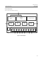
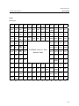
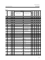
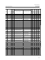
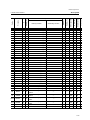
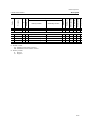
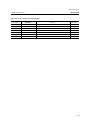
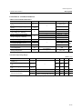
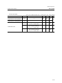
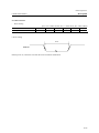
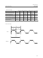
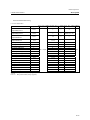
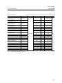
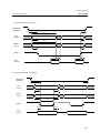
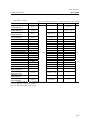
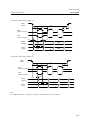
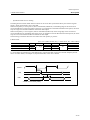
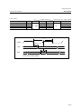
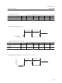
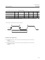
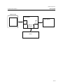
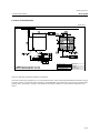
FEDL67Q5250-03 Issue Date: Sep. 2, 2008 ML67Q5250 DFT Based Fingerprint Authentication LSI GENERAL DESCRIPTION The ML67Q5250 is a single chip LSI that executes fingerprint authentication without external memory by using the embedded fingerprint authentication accelerator. This fingerprint authentication accelerator uses DFT(Discrete Fourier Transform) based algorithm licensed from Precise Biometrics, and supports AuthenTec's slide sensors and certain touch sensors from several sensor manufacturers. Besides the ML67Q5250 has the secure circuit to protect enrolled fingerprint data from unauthorized access. Thus this LSI helps customers quickly design new products that offer convenient security as far as high performance fingerprint authentication, low cost and high level of security. FEATURES Fingerprint authentication - DFT (Discrete Fourier Transform) based algorithm licensed from Precise Biometrics This DFT based algorithm achieves a lower FTE (False To Enrollment rate) and a higher authentication accuracy especially when a slide sensor is used, as compared to the minutiae algorithm. - Easy-to-use The fingerprint authentication is performaed by the fingerprint authentication accelerator, which does not ask customers for so complicated control. - No external memory Customer’s application program and up to 15 fingerprint data can be stored in the embedded Flash memory on the ML67Q5250. No external memory is required, when a slide sensor is used. External memory is required when a touch sensor is used. - High-speed authentication, besides low power consumption The highly optimized fingerprint authentication accelerator achieves high-speed authentication using a low speed clock. Authentication : < 0.8 seconds (1:1 authentication) < 1.8 seconds (1:15 authentication) Enrollment : < 2 seconds/finger - Applicable fingerprint sensor Slide sensor : AuthenTec AES1510 (128 8 pixels) AuthenTec AES2510 (192 16 pixels) Touch sensor : Any vendor’s touch sensor as far as 256 360 pixels max., 8 bits/pixel and 5008 dpi CPU - 32-bit RISC CPU (ARM7TDMI) - Little endian format - Instruction system: A high-density 32-bit instruction and a 16-bit instruction of high-object efficiency, which is the subset of the 32-bit instruction, can be executed in mixed mode. - General-purpose register: 32 bits x 31 registers - Built-in barrel shifter (ALU and barrel shift operation can be executed by one instruction) - Built-in debugging function (JTAG interface) The JTAG interface pin is shared with GPIO. 1/36 FEDL67Q5250-03 LAPIS Semiconductor Internal RAM - Working RAM for CPU ML67Q5250 : 16 Kbytes Internal Flash ROM - 128 Kbyte Flash ROM - Program ROM : 64 Kbytes This program ROM includes drivers for fingerprint authentication and peripherals. Erase/rewrite times : 100 max. - Data ROM for storing fingerprint data : 64 Kbytes Erase/rewrite times : 10,000 max. (when enrolling one fingerprint data) External memory controller - ROM/Flash • 1 bank x 4 Mbytes • Supports 16-bit devices • Bootable from external ROM/Flash This function can not be used during security function being activated. - SRAM • 1 bank 4 Mbytes • Supports 16-bit devices - External I/O • 2-bank 4 Mbytes • Supports 8-bit/16-bit devices • Enable to set address setup, RW/WE pulse, and data off timing in system clock cycle unit • Supports an access wait function by wait signal Interrupt control - FIQ: 1 interrupt source - IRQ: 22 interrupt sources 7 priority levels can be set for each source. DMA controller (DMAC) - 2 channels - Enable to allocate multiple DMA transfer request sources for each channel. - Channel priority: fixed mode/round robin mode - DMA transfer mode: cycle steal mode/burst mode - DMA request type: software requests/hardware requests - Maximum transfer count : 65,536 - Data transfer size: 8 bits/16 bits/32 bits - Transfer request source: CPU, SPI, Synchronous SIO, Smartcard IF 2/36 FEDL67Q5250-03 LAPIS Semiconductor ML67Q5250 GPIO - 13 bits 1 channel, 14 bits 1 channel, and 16 bits 1 channel - Enable to setting input mode or output mode for each bit - Enable to setting as interruption source for each bit - Interruption mode: level/edge and positive logic/negative logic System timer - 16-bit auto reload timer 1 channel Flexible timer (FTM) - 16-bit timer 3 channels - Operating mode Auto reload timer (ART) /Compare Out (CMO) /pulse width modulation (PWM) /capture (CAP) mode. Watch dog timer (WDT) - 16-bits timer - 8.389 seconds max. (when CPU operating frequency is 32 MHz) - Enables generation of interrupt or reset by setting SIO (UART) - Full-duplex asynchronous mode - Built-in baud rate generator SPI - 2 channels of full-duplex serial peripheral interfaces - Operating mode: master mode/slave mode - Data transfer size: 8 bits (byte) / 16 bits (word) - Built-in 16-byte/16-word FIFO on the transmission side and the reception side - Supports DMA transfer (master/slave mode) Synchronous SIO (SSIO) - 8-bit clock synchronous serial port 1 channel - Selectable clock polarity - Selectable LSB first or MSB first - Operation mode: master mode/slave mode - Supports DMAC transfer (in master mode only) Smart Card interface (Smartcard IF) - ISO UART 1 channel - Built-in 16-byte FIFO - Built-in parity error counter in receive mode and transmit mode at automatic retransmission - Supports asynchronous protocol of T = 0 and T = 1 according to ISO7816 and EMV - Built-in error detection code generation and error detection functions by hardware - Supports DMA transfer USB2.0 full-speed device - Compliant with Universal Serial Bus (USB) 2.0 - Full speed (12 Mbps) 1 port. - End points: 5 or 6 - Supports all data transfer types (control transfer, bulk transfer, interrupt transfer, isochronous transfer). - Built-in SOF generation and CRC5/16 generation functions - Access size to data transfer FIFOs: 8 bits/16 bits/32 bits 3/36 FEDL67Q5250-03 LAPIS Semiconductor ML67Q5250 Random number generator (RANDOM) - Generates 8-bit random numbers Clock - Input clock: 12 MHz (oscillator connected) - System clock (CPU operating clock): 32 MHz System clock is generated by PLL using 12MHz clock. - Output clock: 6/12 MHz for fingerprint sensor Power management - Power saving mode • Individual module clock stop mode: Clock operation/stop can be set for each functional block. • Sensor interrupt wait mode: Start /stop of finger sensor clock output and internal PLL are selectable. • STOP mode: Start /stop of internal PLL and OSC oscillator circuit are selectable. Package - 144-pin LFBGA (P-LFBGA144-1111-0.80) 4/36 FEDL67Q5250-03 LAPIS Semiconductor ML67Q5250 BLOCK DIAGRAM Figure 1 shows a block diagram of this LSI. JTAG Embedded Flash ROM 128 KB ARM7TDMI rev.3 Interrupt Control RAM 16KB Fingerprint Accelerator DMAC 2ch Memory Controller Peripherals PLL System Timer SIO USB FS Device SPI 2ch GPIO 3 ch (43 bits) FTM 3ch WDT Smart Card IF 1ch SSIO 1ch RAN DOM Figure 1 Block Diagram 5/36 FEDL67Q5250-03 LAPIS Semiconductor ML67Q5250 PINS Pin Layout VDD CORE XD08 XD07 XD15 XD14 GNDIO XD10 XD09 GND PC13 CORE PB04 PB02 TEST0 GNDIO PB07 PB05 PB03T VDDIO PB00X XBNS0 XBSN1 PB06 GND CORE VDDIO XIO1 CSN PB08 VDD CORE PB09 PB10 XIO0 XWAIT XWAIT1 JTAGE PB01 CSN 0N N XREN XROM XWEN GNDIO CSN XD13 PC12 PC11 12 PC10 PC08 XD05 11 PC15 GNDIO PC09 XD03 XD04 10 XD01 VDDIO XD00 XD02 9 GNDIO 8 PC04 VDDIO PC05 PC03 7 PC00 6 PA12 5 XD12 VDDIO PC14 XD11 XD06 TEST1 TESTF 13 XRAMC PB11 SN GND CORE PB12 VDDIO XA01 VDD CORE XA00 XA04 GNDIO XA02 XA03 PC02 TEST3 PC01 XA08 XA06 PA13 GND GNDIO CORE XA11 XI N.C. VDDIO VDD CORE DM 4 PLL VDD PA08 VDD CORE N.C. DP 3 XO PLL GND GND GNDIO PUCTL CORE VDDIO XA05 TEST2 PC06 PC07 P-LFBGA-144-1111-0.80 (Bottom View) XA09 XA07 XA16 PA01 XA21 PA05 XA12 XA10 GNDIO XA18 XA19 N.C. PA04 BOOTP XA13 XA14 VDD CORE PA00 VDDIO XA20 N.C. VDDIO GND CORE XA15 XA17 GNDIO PA02 PA03 GNDIO VDDIO N M L K J H G PA06 PA07 F E RESET PA09 N D C PA10 PA11 B A 2 1 6/36 FEDL67Q5250-03 LAPIS Semiconductor ML67Q5250 Pin List 5V Tolerant Initial direction Initial value I Drive capability — — — — — — I O — — PU 4mA — I — S PD 4mA — I — S PD 4mA — I — — PD 4mA — I — S — I — S PD 4mA — I — S PD 4mA — I — S PD 4mA — I — — — — — PD PD PD PD 4mA 4mA 4mA 4mA — — — — I I I I — — — — — PD 4mA — I — — PD 4mA — I — — PD 4mA — I — — PD 4mA — I — — — PD 4mA PD 4mA — — I I — — — PD 4mA — I — — PD 4mA — I — — PD 4mA — I — S PD 4mA — I — PU/PD (*1) — — Secondary function Schmitt Clock XI XO Reset D1 RESETN JTAG H10 JTAGE GPIO E4 E2 I/O Polarity (*2) Pin name Pin No. Description Oscillation pin Oscillation pin — — — — — — N System reset input — S I P JTAG enable — Primary function D5 PA13 I/O P General-purpose port A13 A5 PA12 I/O P General-purpose port A12 A1 PA11 I P General-purpose port A11 B1 PA10 I/O P General-purpose port A10 C1 PA09 I/O P General-purpose port A9 D3 PA08 I/O P General-purpose port A8 F2 F4 G4 G3 PA07 PA06 PA05 PA04 I/O I/O I/O I/O P P P P General-purpose port A7 General-purpose port A6 General-purpose port A5 General-purpose port A4 G1 PA03 I/O P General-purpose port A3 H1 PA02 I/O P General-purpose port A2 J4 PA01 I/O P General-purpose port A1 K2 PA00 I/O P General-purpose port A0 K8 M8 PB12 PB11 I/O I/O P P General-purpose port B12 General-purpose port B11 M10 PB10 I/O P General-purpose port B10 N10 PB09 I/O P General-purpose port B09 L11 PB08 I/O P General-purpose port B08 L13 PB07 I/O P General-purpose port B07 External interrupt input (Interrupt No. 30) Clock output (for sensor) External interrupt input (USB VBUS interrupt) External interrupt input (Interrupt No. 28) External interrupt input (Interrupt No. 26) External FIQ interrupt input — Smartcard IF clock Smartcard IF reset Smartcard IF serial data Smartcard IF power control Smartcard IF voltage control 1 Smartcard IF voltage control 0 Smartcard IF card detection SIO receive data input SIO transmit data output FTM2 FTMIN[2]/FTMOUT[2] INOUT FTM1 FTMCLK[1] IN/FTMIN[1]/FTMOUT[1] INOUT FTM0 FTMCLK[0] IN/FTMIN[0]/FTMOUT[0] INOUT JTAG clock — 7/36 FEDL67Q5250-03 LAPIS Semiconductor ML67Q5250 General-purpose port B06 General-purpose port B05 General-purpose port B04 General-purpose port B03 H11 PB02 I/O P General-purpose port B02 G10 G13 E10 D11 C12 B12 A12 C11 C10 B11 PB01 PB00 PC15 PC14 PC13 PC12 PC11 PC10 PC09 PC08 I/O I/O I/O I/O I/O I/O I/O I/O I/O I/O P P P P P P P P P P General-purpose port B01 General-purpose port B00 General-purpose port C15 General-purpose port C14 General-purpose port C13 General-purpose port C12 General-purpose port C11 General-purpose port C10 General-purpose port C9 General-purpose port C8 B8 PC07 I/O P General-purpose port C7 C8 PC06 I/O P General-purpose port C6 B7 PC05 I/O P General-purpose port C5 D7 PC04 I/O P General-purpose port C4 A7 PC03 I/O P General-purpose port C3 D6 PC02 I/O P General-purpose port C2 B6 PC01 I/O P General-purpose port C1 A6 PC00 I/O P General-purpose port C0 A4 A3 A2 H4 H2 J3 K3 K1 K4 L1 M2 N2 USB FS Device DM I/O P DP I/O P PUCTL O P External Memory Bus XA21 O P XA20 O P XA19 O P XA18 O P XA17 O P XA16 O P XA15 O P XA14 O P XA13 O P JTAG mode setting JTAG data input JTAG data output JTAG reset SSIO communication clock input/output SSIO receive data input SSIO transmit data output — — — — — — — — SPI ch1 transmit/receive clock SPI ch1 slave select SPI ch1 master input/slave output SPI ch1 master output/slave input SPI ch0 transmit/receive clock SPI ch0 slave select SPI ch0 master input/slave output SPI ch0 master output/slave input Initial value P P P P Initial direction I/O I/O I/O I/O 5V Tolerant PB06 PB05 PB04 PB03 Secondary function Drive capability L12 K13 J11 J13 Primary function PU/PD (*1) Pin name I/O Schmitt Pin No. Polarity (*2) Description S S — S PD PD PD PD 4mA 4mA 4mA 4mA — — — — I I I I — — — — S PD 4mA — I — — — — — — — — — — — PD PD — — — — PD PD PD PD 4mA 4mA 4mA 4mA 4mA 4mA 4mA 4mA 4mA 4mA — — — — — — — — — — I I I I I I I I I I — — — — — S PD 4mA — I S PD 4mA — I — PD 4mA — I — PD 4mA — I S PD 4mA — I S PD 4mA — I — PD 4mA — I — PD 4mA — I USB dev D USB dev D USB dev pull-up control — — — — — — — — — — — 4mA — — — External bus address signal External bus address signal External bus address signal External bus address signal External bus address signal External bus address signal External bus address signal External bus address signal External bus address signal — — — — — — — — — — — — — — — — — — — — — — — — — — — 4mA 4mA 4mA 4mA 4mA 4mA 4mA 4mA 4mA — — — — — — — — — O O O O O O O O O 8/36 FEDL67Q5250-03 LAPIS Semiconductor ML67Q5250 N L9 XWEN O N M12 XBSN1 O N N12 XBSN0 O N K10 J10 XWAIT0N XWAIT1N I I N N Initial value O Initial direction XREN 5V Tolerant N9 Drive capability P P P P P P P P P P P P P P P P P P P P P P P P P P P P P N N N N Secondary function PU/PD (*1) O O O O O O O O O O O O O I/O I/O I/O I/O I/O I/O I/O I/O I/O I/O I/O I/O I/O I/O I/O I/O O O O O Primary function Schmitt N3 XA12 L4 XA11 M3 XA10 N4 XA09 L5 XA08 M4 XA07 K5 XA06 M5 XA05 N6 XA04 K6 XA03 L6 XA02 M7 XA01 K7 XA00 J12 XD15 H12 XD14 G11 XD13 F11 XD12 F10 XD11 F12 XD10 E12 XD09 E13 XD08 D13 XD07 C13 XD06 A11 XD05 A10 XD04 B10 XD03 A9 XD02 D9 XD01 B9 XD00 M9 XROMCSN N8 XRAMCSN L10 XIO0CSN M11 XIO1CSN I/O Polarity (*2) Pin name Pin No. Description External bus address signal External bus address signal External bus address signal External bus address signal External bus address signal External bus address signal External bus address signal External bus address signal External bus address signal External bus address signal External bus address signal External bus address signal External bus address signal External bus data signal External bus data signal External bus data signal External bus data signal External bus data signal External bus data signal External bus data signal External bus data signal External bus data signal External bus data signal External bus data signal External bus data signal External bus data signal External bus data signal External bus data signal External bus data signal External ROM chip select External RAM chip select External IO0 chip select External IO1 chip select External memory read enable External memory write enable External memory byte select External memory byte select External IO0 access wait External IO1 access wait — — — — — — — — — — — — — — — — — — — — — — — — — — — — — — — — — — — — — — — — — — — — — — S S S S S S S S S S S S S S S S — — — — — — — — — — — — — — — — — PU PU PU PU PU PU PU PU PU PU PU PU PU PU PU PU — — — — 4mA 4mA 4mA 4mA 4mA 4mA 4mA 4mA 4mA 4mA 4mA 4mA 4mA 4mA 4mA 4mA 4mA 4mA 4mA 4mA 4mA 4mA 4mA 4mA 4mA 4mA 4mA 4mA 4mA 4mA 4mA 4mA 4mA — — — — — — — — — — — — — — — — — — — — — — — — — — — — — — — — — O O O O O O O O O O O O O I I I I I I I I I I I I I I I I O O O O 0 0 0 0 0 0 0 0 0 0 0 0 0 — — — — — — — — — — — — — — — — 1 1 1 1 — — — 4mA — O 1 — — — 4mA — O 1 — — — 4mA — O 1 — — — 4mA — O 1 — — S S PU 4mA PU 4mA — — I I — — 9/36 FEDL67Q5250-03 LAPIS Semiconductor ML67Q5250 Initial direction Initial value P P P P P 5V Tolerant I I I I I Drive capability P PU/PD (*1) I Secondary function Schmitt For System BOOTP For Testing A13 TESTF N13 TEST0 B13 TEST1 D8 TEST2 C6 TEST3 F3 I/O Polarity (*2) Pin name Pin No. Description Boot device select 1 — S PU 4mA — I — Test pin Test mode select signal 0 Test mode select signal 1 Test mode select signal 2 Test mode select signal 3 — — — — — — S S S S — PD PD PD PD — — — — — I I I I I — — — — — Primary function — 4mA 4mA 4mA 4mA *1: PU/PD column: PU: Pulled up with a built-in resistor PD: Pulled down with a built-in resistor *2: Polarity column: P: Positive N: Negative 10/36 FEDL67Q5250-03 LAPIS Semiconductor ML67Q5250 Other Pins (Power supply pins, Unused pins) Pin name Description VDDCORE Core power supply GNDCORE Pin No. C3, L2, L7, K11, F13, B4 Pin count 6 Core GND C2, M1, L8, K12, D12, C5 6 VDDIO IO power supply E1, J2, N1, N5, N7, N11, H13, E11, C9, C7, C4 11 GNDIO IO GND F1, J1, L3, M6, K9, M13, G12, D10, A8, B5, B2 11 PLLVDD PLL power supply E3 1 PLLGND PLL GND D2 1 Unused pin G2, H3, B3, D4 4 N.C. 11/36 FEDL67Q5250-03 LAPIS Semiconductor ML67Q5250 ELECTRICAL CHARACTERISTICS ABSOLUTE MAXIMUM RATINGS Parameter Symbol Digital power supply voltage CORE (2.5V) Digital power supply voltage I/O (3.3V) Input voltage (normal buffer) Rating VDD_CORE VI Output voltage (normal buffer) VO Output voltage (5 V tolerant) — IOH “L” output allowable current IOL 0.3 to VDD_IO0.3 –0.3 to 6.0 0.3 to VDD_IO0.3 0.3 to VDD_IO0.3 –0.3 to 6.0 0.3 to VDD_IO0.3 –0.3 to +3.6 –10 to +10 — V mA +14 –14 PD Ta = 85°C (per package) 600 mW TSTG — –50 to 150 C Power dissipation Storage temperature –0.3 to +4.6 VDD_IO = 3.0 V to 3.6 V VDD_IO 3.0 V — VDD_IO = 3.0 V to 3.6 V VDD_IO 3.0 V VDD_PLL II “H” output allowable current Unit –0.3 to +3.6 VDD_IO Input voltage (5 V tolerant) PLL power supply voltage (PLL) Input allowable current Condition Guaranteed Operating Ranges Parameter Digital power supply voltage (CORE) (*1) Digital power supply voltage (I/O) PLL power supply voltage (PLL) (*1) CPU operating frequency Ambient temperature Symbol VDD_CORE VDD_IO Ta_flwrite Typ. (GND = 0 V) Max. Unit 2.25 2.5 2.75 3.0 3.3 3.6 2.25 2.5 2.75 — –40 32 25 — 85 MHz C –40 25 70 C — VDD_PLL fOSC Ta Min. Condition — Other than below - When enrolling fingerprints - When rewriting Flash memory V * 1: Please supply from same power source to both VDD_CORE pins and VDD_PLL pin. 12/36 FEDL67Q5250-03 LAPIS Semiconductor – ML67Q5250 Internal Flash ROM Parameter Guaranteed ambient temperature for write operations Guaranteed ambient temperature for read operations Symbol (VDD_CORE = 2.25 to 2.75 V, VDD_IO = 3.0 to 3.6 V, Ta = 40 to 85C) Condition Min. Typ. Max. Unit Ta_flwrite –40 25 70 °C Ta_flread CWR_CODE Flash write count — CWR_DATA01 CWR_DATA15 — Program code rewrite Ta_flwrite = –40 to +70°C Fingerprint template data rewrite (for 1-finger enrollment) Ta_flwrite = 40 to 70C Fingerprint template data rewrite (for 15-finger enrollment) Ta_flwrite = 40 to 70C –40 25 85 — — 100 — — — 10,000 — — — 1,000 — 13/36 FEDL67Q5250-03 LAPIS Semiconductor ML67Q5250 DC Characteristics – DC characteristics (Core/IO) Parameter “H” input voltage “L” input voltage Schmitt trigger input threshold voltage (3.3 V) Schmitt trigger input threshold voltage (5 V tolerant) “H” output voltage “L” output voltage High level input current (*1) High level input current (*2) Low level input current (*1) Symbol (VDD_CORE = 2.25 to 2.75 V, VDD_IO = 3.0 to 3.6 V, Ta = 40 to 85C) Condition Min. Typ. Max. Unit VIH VIL VT+ VTVT VT+ VTVT VOH 2.0 –0.3 — VDD_IO 0.2 VDD_IO 0.1 — VDD_IO 0.2 VDD_IO 0.1 2.4 — — — — — — — — — VDD_IO 0.3 0.8 VDD_IO 0.7 — — VDD_IO 0.7 — — — IOL = 4 mA VIH = VDD_IO 50 k pull-down VIH = VDD_IO VIH = 5.5 V VIL = 0 V — — 10 — — –10 — — 66 — — — 0.4 10 200 10 10 — 50 k pull-up –200 –66 –10 VIL = 0 V –10 — — VOH = VDD_IO — — 10 10 66 200 –10 –200 — — — — — — — — — — –66 — 25 — 4 — 1 85 7 6 — –10 1000 — 200 — 50 — 115 15 10 VOL IIH IIL Low level input current (*2) 3-state output leakage current IOZH IOZL IDDS1_CORE Supply current (during STOP) (*4) IDDS1_IO IDDS1_PLL Supply current (during operation) (*5) IDDO_CORE IDDO_IO IDDO_PLL — VT+ VT— VT+ VTIOH = 4 mA 50 k pull-down VOL = 0 V 50 k pull-up VDD_CORE = 2.75 V, Ta = 85C VDD_CORE = 2.5 V, Ta = 25C VDD_IO = 3.6 V (*3), Ta = 85C VDD_IO = 3.3 V (*3), Ta = 25C VDD_PLL = 2.75 V, Ta = 85C VDD_PLL = 2.5 V, Ta = 25C fOSC = 32.0 MHz , no load V A A A mA * 1: Pins other than 5 V tolerant pins * 2: 5 V tolerant pins * 3: Input ports: VDD_IO or 0V Other ports: No load excluding the current flowing in pull-up/pull-down resistors * 4: LSI supply current when going into LSI stop mode by stopping clock oscillation, PLL operation, and random number generator operation and setting USB power-down mode. * 5: The current supplied to the LSI when fingerprint authentication is executed without USB operation under the conditions that the programs are stored in the built-in Flash ROM and no external memory are connected. 14/36 FEDL67Q5250-03 LAPIS Semiconductor – ML67Q5250 DC characteristics (USB) Parameter Symbol (VDD_CORE = 2.25 to 2.75V, VDD_IO = 3.0 to 3.6V, Ta = 40 to 85C) Condition Min. Typ. (*1) Max. Unit Absolute value of the difference between the DP and DM pins Includes VDI range Differential input sensitivity VDI Differential common mode range Single end input threshold voltage VCM VSE High level output voltage VOH Low level output voltage Hi-Z state input/output leakage current Driver output resistance (*2) VOL 15K W RL is connected to GND 1.5K W RL to 3.6 V ILO 0 V < VIN < 3.3 V ZDRV Steady state 0.2 — — V 0.8 0.8 — — 2.5 2.0 V V 2.8 — — V — — 0.3 V –10 10 A 28 44 *1: “Typ.”: VDD_IO = 3.3 V, VDD_CORE = 2.5 V, Tj = 25°C *2: ZDRV includes the resistance of external serial resistors (241%). 15/36 FEDL67Q5250-03 LAPIS Semiconductor ML67Q5250 AC Characteristics – Reset Timing Parameter Reset pulse width (VDD_CORE = 2.25 to 2.75 V, VDD_IO = 3.0 to 3.6 V, Ta = 40 to 85C) Symbol Condition Min. Typ. Max. Unit tRSTW — 6.0 — — ms Reset timing tRSTW RESETN *When power on, release the reset after the clock oscillation stabilization 16/36 FEDL67Q5250-03 LAPIS Semiconductor – ML67Q5250 Main Clock Timing (VDD_CORE = 2.25 to 2.75 V, VDD_IO = 3.0 to 3.6 V, Ta = 40 to 85C) Symbol Condition Min. Typ. Max. Unit Parameter Main clock (XI/XO) frequency fSYSC — Main clock (XI/XO) cycle tSYSC — Main clock (XI/XO) H pulse width tSYSCH — Main clock (XI/XO) L pulse width tSYSCL — Bus clock cycle (*1) tBUSCLK — 12 0.9975 83.33 0.9975 0.45 tSYSC 0.45 tSYSC — 12 83.33 — — 31.25 12 1.0025 83.33 1.0025 0.55 tSYSC 0.55 tSYSC — MHz ns ns ns ns * 1: Main system bus clock within the LSI and operating clocks of CPU, DMA, etc. Main clock timing tSYSC tSYSCH tSYSCL XI/XO tBUSCLK BUSCLK 17/36 FEDL67Q5250-03 LAPIS Semiconductor – ML67Q5250 External ROM/RAM Timing Access from CPU Parameter XROMCSN, XRAMCSN output delay time 1 XROMCSN, XRAMCSN output delay time 2 XROMCSN, XRAMCSN output hold time 1 XROMCSN, XRAMCSN output hold time 2 XA output delay time 1 XA output delay time 2 XA output hold time 1 XA output hold time 2 XA pulse width 1 XBSn output delay time 1 XBSn output delay time 2 XBSn output hold time 1 XBSn output hold time 2 XBSn pulse width 1 XWEN pulse width 1 XD input setup time 1 XD input setup time 2 XD input hold time 1 XD input hold time 2 XD output delay time 1 XD output hold time 1 Symbol (VDD_CORE = 2.25 to 2.75 V, VDD_IO = 3.0 to 3.6 V, Ta = 40 to 85C) Condition Min. Typ. Max. Unit tXCSD1 — — 4 tXCSD2 — — 0.5*tBUSCLK +8 tXCSH1 –6 — — tXCSH2 0.5*tBUSCLK 6 — — tXAD1 tXAD2 tXAH1 tXAH2 tXAW1 tXBSD1 tXBSD2 tXBSH1 tXBSH2 tXBSW1 tXWEW1 tXDIS1 tXDIS2 tXDIH1 tXDIH2 tXDOD1 tXDOH1 — — –6 0 — — — — — — — — — — — — — — — — — 4 0.5*tBUSCLK +8 — — tRWIDTH +12 4 0.5*tBUSCLK +8 — — tRWIDTH +12 tWWIDTH +13 — — — — — — CL = 15 pF tRWIDTH –12 — — –6 0.5*tBUSCLK –6 tRWIDTH –12 tWWIDTH –13 22.5 22.5 0 0 0.5*tBUSCLK - 13 0 ns tRWIDTH: RE pulse width (set by register) tWWIDTH: WE pulse width (set by register) 18/36 FEDL67Q5250-03 LAPIS Semiconductor ML67Q5250 Access by DMA Parameter XROMCSN, XRAMCSN output delay time 1 XROMCSN, XRAMCSN output delay time 2 XROMCSN, XRAMCSN output hold time 1 XROMCSN, XRAMCSN output hold time 2 XA output delay time 1 XA output delay time 2 XA output hold time 1 XA output hold time 2 Symbol (VDD_CORE = 2.25 to 2.75 V, VDD_IO = 3.0 to 3.6 V, Ta = 40 to 85C) Condition Min. Typ. Max. Unit tXCSD1 — — 1*tBUSCLK +4 tXCSD2 — — 0.5*tBUSCLK +8 tXCSH1 1*tBUSCLK –6 — — tXCSH2 0.5*tBUSCLK –6 — — tXAD1 tXAD2 tXAH1 tXAH2 — — — — — — 1*tBUSCLK +4 1.5*tBUSCLK +10 — — tBUSCLK + tRWIDTH +12 1*tBUSCLK +4 1.5*tBUSCLK +8 — — tBUSCLK + tRWIDTH +12 tWWIDTH +15 —— — ———- XA pulse width 1 tXAW1 XBSn output delay time 1 XBSn output delay time 2 XBSn output hold time 1 XBSn output hold time 2 tXBSD1 tXBSD2 tXBSH1 tXBSH2 XBSn pulse width 1 tXBSW1 XWEN pulse width 1 XD input setup time 1 XD input setup time 2 XD input hold time 1 XD input hold time 2 XD output delay time 1 XD output hold time 1 tXWEW1 tXDIS1 tXDIS2 tXDIH1 tXDIH2 tXDOD1 tXDOH1 CL = 15 pF 1*tBUSCLK –6 0 tBUSCLK + tRWIDTH –12 — — 1*tBUSCLK –6 0.5*tBUSCLK –6 tBUSCLK + tRWIDTH –12 tWWIDTH –15 22.5 22.5 0 0 1.5*tBUSCLK – 13 0 — — — — — — — — — —— — — ns tRWIDTH: RE pulse width (set by register) tWWIDTH: WE pulse width (set by register) 19/36 FEDL67Q5250-03 LAPIS Semiconductor ML67Q5250 External ROM/RAM read timing XROMCSN/ XRAMCSN XAn (n=0-21) XBSNn (n=0-1) tXCSH1 tXCSD1 tXAW1 tXAD1 tXAH1 tXBSW1 tXBSD1 tXBSH1 XREN tXDIS1 tXDIH1 tXDIS2 tXDIH2 XDn (n=0-15) External ROM/RAM write timing XROMCSN/ XRAMCSN tXCSD2 tXCSH2 XAn (n=0-21) tXAD2 tXAH2 XBSNn (n=0-1) tXBSD2 tXWEW1 tXBSH2 XWEN tXDOD1 tXDOH1 XDn (n=0-15) 20/36 FEDL67Q5250-03 LAPIS Semiconductor – ML67Q5250 External IO0, 1 Timing Parameter XIOnCSN (n = 0,1) output delay time 1 XIOnCSN (n = 0,1) output delay time 2 XIOnCSN (n=0,1) output hold time 1 XIOnCSN (n = 0,1) output hold time 2 XA output delay time 3 XA output delay time 4 XA output hold time 3 XA output hold time 4 XA output hold time 5 XBSn output delay time 3 XBSn output delay time 4 XBSn output hold time 3 XBSn output hold time 4 XBSn output hold time 5 XREN pulse width 1 XWEN pulse width 2 XD input setup time 3 XD input hold time 3 XD output delay time 2 XD output hold time 2 XWAITn (n = 0,1) input setup time 1 XWAITn (n = 0,1) input setup time 2 XWAITn (n = 0,1) input hold time 1 XWAITn (n = 0,1) input hold time 2 Symbol (VDD_CORE = 2.25 to 2.75 V, VDD_IO = 3.0 to 3.6 V, Ta = 40 to 85C) Condition Min. Typ. Max. Unit tXIOCSD1 — — tIOAS +8 tXIOCSD2 — — 1*tBUSCLK + tIOAS +8 tXIOCSH1 1*tBUSCLK –6 — — tXIOCSH2 1*tBUSCLK –6 — — tXAD3 tXAD4 tXAH3 tXAH4 tXAH5 tXBSD3 tXBSD4 tXBSH3 tXBSH4 tXBSH5 tXREW1 tXWEW2 tXDIS3 tXDIH3 tXDOD2 tXDOH2 — — –6 1*tBUSCLK –6 1*tBUSCLK –6 — — –6 1*tBUSCLK –6 1*tBUSCLK –6 tIORWIDTH –10 tIOWWIDTH –10 20 0 tIOAS - 13 1*tBUSCLK –15 — — — — — — — — — — — — — — — — tIOAS + 8 1*tBUSCLK + tIOAS +8 — — — tIOAS + 8 1*tBUSCLK + tIOAS +8 — — — tIORWIDTH +10 tIOWWIDTH +10 — — — — tXWAITIS1 1*tBUSCLK + 20 — — tXWAITIS2 1*tBUSCLK + 20 — — tXWAITIH1 5 –1*tBUSCLK — — tXWAITIH2 5 –1*tBUSCLK — — CL = 15 pF ns tIOAS: Address setup cycle (set by register) tIORWIDTH: RE pulse width (set by register) tIOWWIDTH: WE pulse width (set by register) 21/36 FEDL67Q5250-03 LAPIS Semiconductor ML67Q5250 External IO0, 1 read timing XIOnCSN (n=0,1) tXIOCSH1 tXIOCSD1 XAn (n=0-21) tXAD3 tXAH3 tXAH4 XBSNn (n=0-1) tXBSD3 tXBSH3 tXREW1 tXBSH4 XREN tXDIS3 tXDIH3 XDn (n=0-15) XWAITnN (n=0,1) tXWAITIS1 tXWAIT IH1 External IO0, 1 write timing XIOnCSN (n=0,1) tXIOCSH2 tXIOCSD2 XAn (n=0-21) tXAD4 tXAH5 XBSNn (n=0-1) tXBSD4 tXWEW2 tXBSH5 XWEN tXDOD2 tXDOH2 XDn (n=0-15) XWAITnN (n=0,1) tXWAIT IS2 tXWAIT IH2 22/36 FEDL67Q5250-03 LAPIS Semiconductor – ML67Q5250 USB Access Timing (Full-Speed) (VDD_CORE = 2.25 to 2.75 V, VDD_IO = 3.0 to 3.6 V, Ta = 40 to 85C) Parameter Rise time (*1) Fall time (*1) Output signal crossover voltage Data rate Symbol Condition Min. Typ. Max. Unit TR TF CL = 50 pF CL = 50 pF 4 4 — — 20 20 ns ns VCRS CL = 50 pF 0.8 — 2.5 V TDRATE Average bit rate (12Mbps 0.25%) 11.97 — 12.03 Mbps Applied pin DP,DM * 1: TR and TF: Rise time and fall time between 10% and 90% of the pulse amplitude, respectively 23/36 FEDL67Q5250-03 LAPIS Semiconductor – ML67Q5250 SPI Access Timing Characteristics of master mode timing Parameter Data delay time (output) Data setup time (input) Data hold time (input) SSN-SCK lead time SCK-SSN lag time (VDD_CORE = 2.25 to 2.75 V, VDD_IO = 3.0 to 3.6 V, Ta = 40 to 85C) Symbol Condition Min. Typ. Max. Unit tDD tSD tHD CL = 30 pF tLEAD tLAG — 25 0 (*1) 0.5*tSCK - 15 0.5*tSCK - 15 — — — — — 25 — — 1.5*tSCK + 15 1.5*tSCK + 15 ns ns ns ns(*2) ns(*2) * 1: Although actual values may become negative depending on the external load, input the serial data so that the data hold time can be guaranteed. * 2: tSCK is the cycle time of the serial clock for SPI transferring which is obtained by dividing the frequency of the bus clock, whose cycle time is tBUSCLK. For more details, see Chapter 15, “SPI”, in the user’s manual. Characteristics of slave mode timing Parameter Serial clock cycle time Serial clock High/Low time Data delay time (output) Data setup time (input) Data hold time (input) SSN-SCK lead time (VDD_CORE = 2.25 to 2.75 V, VDD_IO = 3.0 to 3.6 V, Ta = 40 to 85C) Symbol Condition Min. Typ. Max. Unit tSCK tWSCK tDD tSD tHD tLEAD — — — — — — SCK-SSN lag time tLAG — Slave data invalid time tDIS — 2 1 — 25 25 25 tBUSCLK + 10 — — — — — — — — — 25 — — — tBUSCLK tBUSCLK ns ns ns ns — — ns — 25 ns 24/36 FEDL67Q5250-03 LAPIS Semiconductor ML67Q5250 SPI master mode timing (CPHA = 0) SSN (Output) tLEAD tLAG tSCK SCK (CPOL=0, Output) SCK (CPOL=1, Output) tSD MISO (Input) tHD LSB MSB tDD tDD MOSI (Output) LSB MSB SPI master mode timing (CPHA = 1) SSN (Output) tLEAD tSCK tLAG SCK (CPOL=0, Output) SCK (CPOL=1, Output) tSD MISO (Input) tHD LSB MSB tDD MOSI (Output) LSB MSB Note: For CPHA and CPOL, see Chapter 15, “SPI”, in the ML67Q5250 User’s Manual. 25/36 FEDL67Q5250-03 LAPIS Semiconductor ML67Q5250 SPI slave mode timing (CPHA = 0) SSN (Input) tSCK tLEAD tLAG SCK (CPOL=0, Input) tWSCK tWSCK SCK (CPOL=1, Input) tDIS tDD MISO (Output) LSB tSD MOSI (Input) MSB tHD LSB MSB SPI slave mode timing (CPHA = 1) SSN (Input) tLEAD SCK (CPOL=0, Input) tSCK tWSCK tLAG tWSCK SCK (CPOL=1, Input) tDD MISO (Output) LSB tSD MOSI (Input) MSB tHD LSB MSB Note: For CPHA and CPOL, see Chapter 15, “SPI”, in the ML67Q5250 User’s Manual. 26/36 FEDL67Q5250-03 LAPIS Semiconductor – ML67Q5250 Synchronous SIO Access Timing Switching between master mode and slave mode can be set for this synchronous SIO by the software register setting. Serial clock polarity can be switched. When clock polarity is set to positive, data is transmitted (shifted out) on the falling edge of the clock and is received (shifted in) on the rising edge of the clock. At completion of 8-bit data transmission/reception, the clock stops at a high level and the last data is retained for data output. When clock polarity is set to negative, data is transmitted (shifted out) on the rising edge of the clock and is received (shifted in) on the falling edge of the clock. At completion of 8-bit data transmission/reception, the clock stops at a low level and the last data is retained for data output. The following waveforms show the cases where the clock polarity is positive. Maste mode Parameter Output data delay time Input data setting time Input data retained time Symbol tMSSOD tMSSIS tMSSIH (VDD_CORE = 2.25 to 2.75 V, VDD_IO = 3.0 to 3.6 V, Ta = 40 to 85C) Condition Min. Max. Unit Remarks — 20 ns CL = 30 pF 30 — 10 — Note: 11 clock outputs for transferring is selectable from 2 synchronous SIO clock sources and the frequency divide ratios. For more details, see Chapter 16, Synchronous SIO, in the user’s manual. SIOCK * tMSSOD TXD tMSSIS tMSSIH RXD * Serial clock: Positive polarity 27/36 FEDL67Q5250-03 LAPIS Semiconductor ML67Q5250 Slave mode Parameter Serial clock cycle Output data delay time Input data setting time Input data retained time Symbol T tSSSOD tSSSIS tSSSIH (VDD_CORE = 2.25 to 2.75 V, VDD_IO = 3.0 to 3.6 V, Ta = 40 to 85C) Condition Min. Max. Unit Remarks 62.5 — — 40 CL = 30 pF ns 20 — 20 — T SIOCK * tSSSOD TXD tSSSIS tSSSIH RXD * Serial clock: Positive polarity 28/36 FEDL67Q5250-03 LAPIS Semiconductor – ML67Q5250 FTM Access Timing Parameter FTMCLKn input H duration FTMCLKn input L duration Symbol TFTMCLKH TFTMCLKL (VDD_CORE = 2.25 to 2.75 V, VDD_IO = 3.0 to 3.6 V, Ta = 40 to 85C) Condition Min. Typ. Max. Unit — — tBUSCLK 2 tBUSCLK 2 — — — — ns ns Note 1: n = 0 to 2 FTMCLKn input timing (n = 0 to 2) TFTMCLKH TFTMCLKL FTMCLKn/ – GPIO (PA, PB, PC) Access Timing Parameter PAn, PBm, PCj input H duration PAn, PBm, PCj input L duration Symbol (VDD_CORE = 2.25 to 2.75 V, VDD_IO = 3.0 to 3.6 V, Ta = 40 to 85C) Condition Min. Typ. Max. Unit TGPIOIH — tBUSCLK 2 — — ns TGPIOIL — tBUSCLK 2 — — ns Note 1: n = 12 to 0, m=13 to 0, j = 15 to 0 PAn,PBm,PCj input timing (n = 12 to 0, m = 13 to 0, j = 15 to 0) TGPIOIH TGPIOIL PAn/ PBm/ PCj/ 29/36 FEDL67Q5250-03 LAPIS Semiconductor – ML67Q5250 Clock Output (Secondary Function of PA12 Pin) Timing (VDD_CORE = 2.25 to 2.75 V, VDD_IO = 3.0 to 3.6 V, Ta = 40 to 85C) Condition Min. Typ. Max. Unit Parameter Symbol Clock output High duration tCLKOUT_H — Clock output Low duration tCLKOUT_L — Rise time Fall time tR_CLKOUT tF_CLKOUT CL = 10 pF CL = 10 pF 45% tCLKOUT 45% tCLKOUT 50% tCLKOUT 50% tCLKOUT 55% tCLKOUT 55% tCLKOUT 3 3 ns (*1) ns (*1) ns ns *: tCLKOUT is the cycle time of the 6 MHz or 12 MHz clock generated by 2 clock sources and the frequency divide ratio. (refer Chapter 4 in detail in the user’s manual) Clock output (secondary function of PA12 pin) timing tR_CLKOUT tF_CLKOUT tCLKOUT_H tCLKOUT _L tCLKOUT POWER ON/OFF SEQUENCE Turn on the following powers in this order or turn on all the following powers at the same time. 1. VDDIO 2. VDDCORE, PLLVDD Turn off the following powers in this order or turn off all the following powers at the same time. 1. VDDCORE, PLLVDD 2. VDDIO 30/36 FEDL67Q5250-03 LAPIS Semiconductor ML67Q5250 EXAMPLES OF APPLICATION - Notebook PC - USB token etc… ML67Q5250 AuthenTec AES1510/AES2510 Main System SPI 1 or 2ch USB FS Clock - Gate system - Printer etc… AuthenTec AES1510/AES2510 ML67Q5250 Main System SPI 1 or 2ch USB FS Clock SmartCard I/F ID information SmartCard 31/36 FEDL67Q5250-03 LAPIS Semiconductor ML67Q5250 Touch sensor ML67Q5250 Main System USB FS SPI Memory Controller SRAM 32/36 FEDL67Q5250-03 LAPIS Semiconductor ML67Q5250 PACKAGE DIMENSIONS (Unit: mm) P-LFBGA144-1111-0.80 5 Package material Ball material Package weight (g) Rev. No./Last Revised Epoxy resin Sn/Ag/Cu 0.30 TYP. 1/Jul. 23, 2002 Notes for Mounting the Surface Mount Type Package The surface mount type packages are very susceptible to heat in reflow mounting and humidity absorbed in storage. Therefore, before you perform reflow mounting, contact ROHM’s responsible sales person for the product name, package name, pin number, package code and desired mounting conditions (reflow method, temperature and times). 33/36 FEDL67Q5250-03 LAPIS Semiconductor ML67Q5250 REVISION HISTORY Document No. Date PEDL67Q5250-1 FEDL67Q5250-1 Nov. 9, 2007 Feb.22, 2008 Page Previous Current Edition Edition – – – – 11 11 12 to 30 12 to 30 12 12 14 14 15 15 18, 19 18, 19 21 21 23 23 Description Preliminary edition 1 Final edition 1 Corrected "Core power supply" to "IO power supply" at Description of VDDIO in the Table of Other Pins. Corrected "Core GND" to "IO GND" at Description of GNDIO in the Table of Other Pins. Deleted all the sentences of "Note: The values in the table above are preliminary and are subject to change without notice." indicated in Chapter 22 of the preliminary version. Added "(*1)" to "Digital power supply voltage (CORE)" and "PLL power supply voltage (PLL)" in the specification table of Guaranteed Operating Ranges. Added " * 1: Please supply from same power source to both VDD_CORE pins and VDD_PLL pin." to the margin of this specification table. Changed "Taflw" into "Ta_flwrite" with the sign of the item of the ambient temperature of this table. Changed the specification value of "Supply current (during operation)" in the specification table of DC characteristics (Core/IO) Added "*5: The current supplied to the LSI…" at the lower column of the specification table of DC characteristics (Core/IO). Changed "|(YB)-(YBN)|" into “Absolute value of the difference between the DP and DM pins” at the condition column of "Differential input sensitivity" in the specification table of DC characteristics (USB). Deleted the maximum specification of "High level output voltage" and the minimum specification of "Low level output voltage" in the specification table of DC characteristics (USB). Changed the several specification values in the two tables of "Access from CPU" and "Access by DMA" of External ROM/RAM Timing. Changed the several specification value in the specification table of External IO0, 1 Timing. Changed the specification value of "Output signal crossover voltage" in the specification table of USB Access Timing (Full-Speed). 34/36 FEDL67Q5250-03 LAPIS Semiconductor ML67Q5250 Document No. Date FEDL67Q5250-01 Feb.22, 2008 FEDL67Q5250-02 FEDL67Q5250-03 Mar.31, 2008 Sep.02, 2008 Page Previous Current Edition Edition 24 24 27 27 30 30 – 1 – 1 2 2 16 16 Description Deleted the column of “Serial clock cycle time”, “Serial clock High/Low time”, “SSN H min. guaranteed time”, “SPI bus input/output rise/fall time” in the Characteristics table of master mode timing in “-SPI Access Timing.” Changed the specification value of "SSN-SCK lead time" and "SCK-SSN lag time" in this table. Added the note of *2 at the lower column of this specification table. Changed the specification value of "SCK-SSN lag time" in the table of "Characteristics of slave mode timing.” Deleted the column of "SPI bus input/output rise/fall time" in this table. Changed the specification value of master mode in “Synchronous SIO Access Timing.” Added the note at the lower column of this specification table. Added the note of *1 at the lower column of the specification table of “- Clock Output (Secondary Function of PA12 Pin) Timing.” Final Edition 2 Modified description “DTF” to “DFT” in fingerprint authentication of FEATURES. Deleted description about Fingerprint authentication RAM in Internal RAM of FEATURES. Added a notes to the reset input timing at the time of a power supply injection, in the section of Reset Timing. 35/36 FEDL67Q5250-03 LAPIS Semiconductor ML67Q5250 NOTICE No copying or reproduction of this document, in part or in whole, is permitted without the consent of LAPIS Semiconductor Co., Ltd. The content specified herein is subject to change for improvement without notice. The content specified herein is for the purpose of introducing LAPIS Semiconductor's products (hereinafter "Products"). If you wish to use any such Product, please be sure to refer to the specifications, which can be obtained from LAPIS Semiconductor upon request. Examples of application circuits, circuit constants and any other information contained herein illustrate the standard usage and operations of the Products. The peripheral conditions must be taken into account when designing circuits for mass production. Great care was taken in ensuring the accuracy of the information specified in this document. However, should you incur any damage arising from any inaccuracy or misprint of such information, LAPIS Semiconductor shall bear no responsibility for such damage. The technical information specified herein is intended only to show the typical functions of and examples of application circuits for the Products. LAPIS Semiconductor does not grant you, explicitly or implicitly, any license to use or exercise intellectual property or other rights held by LAPIS Semiconductor and other parties. LAPIS Semiconductor shall bear no responsibility whatsoever for any dispute arising from the use of such technical information. The Products specified in this document are intended to be used with general-use electronic equipment or devices (such as audio visual equipment, office-automation equipment, communication devices, electronic appliances and amusement devices). The Products specified in this document are not designed to be radiation tolerant. While LAPIS Semiconductor always makes efforts to enhance the quality and reliability of its Products, a Product may fail or malfunction for a variety of reasons. Please be sure to implement in your equipment using the Products safety measures to guard against the possibility of physical injury, fire or any other damage caused in the event of the failure of any Product, such as derating, redundancy, fire control and fail-safe designs. LAPIS Semiconductor shall bear no responsibility whatsoever for your use of any Product outside of the prescribed scope or not in accordance with the instruction manual. The Products are not designed or manufactured to be used with any equipment, device or system which requires an extremely high level of reliability the failure or malfunction of which may result in a direct threat to human life or create a risk of human injury (such as a medical instrument, transportation equipment, aerospace machinery, nuclear-reactor controller, fuel-controller or other safety device). LAPIS Semiconductor shall bear no responsibility in any way for use of any of the Products for the above special purposes. If a Product is intended to be used for any such special purpose, please contact a ROHM sales representative before purchasing. If you intend to export or ship overseas any Product or technology specified herein that may be controlled under the Foreign Exchange and the Foreign Trade Law, you will be required to obtain a license or permit under the Law. Copyright 2008 - 2011 LAPIS Semiconductor Co., Ltd. 36/36