1
MAX24104
15Gbps Quad Linear Equalizer
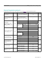
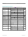
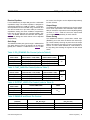
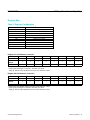
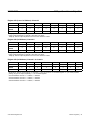
Electrical Characteristics (continued)
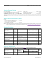
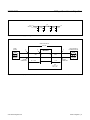
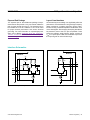
(Typical values are at VCCR = VCCT = VCCP = 2.5V, TA = +25°C. See Figure 1 for typical supply filtering.) (Note 2)
PARAMETER
SYMBOL
CONDITIONS
MIN
TYP
MAX
UNITS
0.3 x
VCC
V
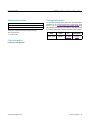
I2C CHARACTERISTICS (SDA, SCL) (Note 7)
Low-Level Input Voltage
VIL
High-Level Input Voltage
VIH
Input Hysteresis
0.7 x
VCC
V
VHYS
200
Input Capacitance
CIN
10
Input Leakage Current
IIN
Output Low Voltage SDA
SCLK Clock Frequency
VOL
fSCLK
mV
pF
±1
ISINK = 3mA
0.4
ISINK = 6mA
0.6
400
mA
V
kHz
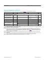
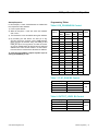
Note 2: The MAX24104 is 100% production tested at TA = +25°C and TA = +85°C. Specification at TA = -40°C is guaranteed by
design or characterization, unless otherwise noted.
Note 3: Guaranteed by design and characterization.
Note 4: Measured with circuit board loss optimized for best DJ. Residual jitter is the difference in deterministic jitter between the
reference data source and device output. DJRESIDUAL = DJOUTPUT – DJSOURCE. The deterministic jitter at the output
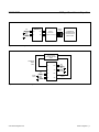
of the transmission line must be from media induced loss. Measured at point D in Figure 2. Test Pattern: 66 Zeroes, 1010,
PRBS7, 66 ones, 0101 Inverted PRBS7.
Note 5: The output voltage range in which a linear relationship between the input and output maintains less than or equal to 1dB
compression.
Note 6: Measured using a vector-network analyzer (VNA N5245A) with -15dBm power level applied to the adjacent input. The VNA
detects the signal at the output of the victim channel. All other inputs and outputs are terminated with 50Ω.
Note 7: Refer to UM10204: I2C-bus specification and user manual, Rev. 03 – 19 June 2007.
www.maximintegrated.com
Maxim Integrated │ 5