1
Embedded Solutions
20F207-00 E2 – 2008-07-21
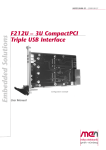
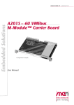
F207 – 3U CompactPCI®
Carrier Board for PCI-104
Configuration example
User Manual
®
F207 – 3U CompactPCI® Carrier Board for PCI-104
F207 – 3U CompactPCI® Carrier Board for PCI-104
The F207 is a 3U CompactPCI® bus card which provides a PCI-104 interface
supporting up to four PCI-104 extension boards. An on-board PCI-to-PCI bridge
provides a 32-bit PCI interface at the PCI-104 connector and a 32-bit/33-MHz
interface to the CompactPCI® bus. V(I/O) voltage is 3.3V on the local bus (5V on
request) and 3.3V or 5V on CompactPCI®.
Two different versions of the F207 offer two different connector positions where a
PCI-104 module can be placed. The standard version supports the typical stacking
method of PCI-104 devices and needs more than one slot of space in a
CompactPCI® system. Another version allows face-to-face assembly.
The F207 is fully compliant with railway standard EN 50155. For example, all
components are specified for an operation temperature of -40 to +85°C.
Technical Data
PCI-104
• One slot for PCI-104
• Up to four stacked PCI-104 modules
• 8HP solution with one PCI-104 module mounted
- Second front panel as needed (filler panel or with connector cut-outs)
Peripheral Connections
• Via front panel
Local PCI Bus
• 32-bit/33-MHz, 3.3V or 5V (on request) V(I/O)
• Compliant with PCI Specification 2.2
CompactPCI® Bus
•
•
•
•
Compliance with CompactPCI® Core Specification PICMG 2.0 R3.0
Peripheral slot
Only one slot required on 3U CompactPCI® bus
PCI2050 PCI-to-PCI bridge
- Max. clock frequency 33MHz
- 32-bit/33-MHz PCI-to-PCI bridge
• V(I/O): +3.3V or +5V (Universal Board)
MEN Mikro Elektronik GmbH
20F207-00 E2 – 2008-07-21
2
Technical Data
Electrical Specifications
• Supply voltage/power consumption:
- +5V (-3%/+5%), 40mA max. (without PCI-104 module)
- +3.3V (-3%/+5%), 60mA max. (without PCI-104 module)
Mechanical Specifications
• Dimensions: conforming to CompactPCI® specification for 3U boards
• Front panel: aluminum with 1 handle
• Weight: 170g
Environmental Specifications
• Temperature range (operation):
- -40..+85°C
- Airflow: min. 10m³/h
• Temperature range (storage): -40..+85°C
• Relative humidity (operation): max. 95% non-condensing
• Relative humidity (storage): max. 95% non-condensing
• Altitude: -300m to + 3,000m
• Shock: 15g/11ms
• Bump: 10g/16ms
• Vibration (sinusoidal): 2g/10..150Hz
• Conformal coating on request
MTBF
• MTBF: 2,006,823h @ 40°C
Safety
• PCB manufactured with a flammability rating of 94V-0 by UL recognized
manufacturers
EMC
• Tested according to EN 55022 (radio disturbance), IEC1000-4-2 (ESD) and
IEC1000-4-4 (burst) with regard to CE conformity
Software Support
• PCI-104 drivers as supported
• For more information on supported operating system versions and drivers see
online data sheet.
MEN Mikro Elektronik GmbH
20F207-00 E2 – 2008-07-21
3
Block Diagram
Block Diagram
PCI-104
PCI-104
Module
PCI-104
Module
PCI-104
Module
Module
MEN Mikro Elektronik GmbH
20F207-00 E2 – 2008-07-21
PCI-104
Connector
PCI-to-PCI
Bridge
CompactPCI J1
4
Configuration Options
Configuration Options
PCI-104 Slot
• One PCI-104 module mounted "face-to-face" instead of PCI-104 stacking
• 4HP solution with one PCI-104 module mounted (single-slot)
• Only for PCI-104 modules that have a modified or no PCI-104 connector on the
bottom side, because of height restriction to 4HP
V(I/O) on Local Bus
• 5V instead of 3.3V
Please note that some of these options may only be available for large volumes.
Please contact MEN’s sales team for further information.
MEN Mikro Elektronik GmbH
20F207-00 E2 – 2008-07-21
5
Product Safety
Product Safety
!
Electrostatic Discharge (ESD)
Computer boards and components contain electrostatic sensitive devices.
Electrostatic discharge (ESD) can damage components. To protect the board and
other components against damage from static electricity, you should follow some
precautions whenever you work on your computer.
• Power down and unplug your computer system when working on the inside.
• Hold components by the edges and try not to touch the IC chips, leads, or circuitry.
• Use a grounded wrist strap before handling computer components.
• Place components on a grounded antistatic pad or on the bag that came with the
component whenever the components are separated from the system.
• Store the board only in its original ESD-protected packaging. Retain the original
packaging in case you need to return the board to MEN for repair.
MEN Mikro Elektronik GmbH
20F207-00 E2 – 2008-07-21
6
About this Document
About this Document
This user manual describes the hardware functions of the board, connection of
peripheral devices and integration into a system. It also provides additional
information for special applications and configurations of the board.
The manual does not include detailed information on individual components (data
sheets etc.). A list of literature is given in the appendix.
History
Edition
Comments
Technical Content
Date of Issue
E1
First edition
R. Weisbach
2005-09-30
E2
Added MTBF information
R. Weisbach
2008-07-21
Minor corrections
regarding technical data
Conventions
!
italics
bold
monospace
hyperlink
This sign marks important notes or warnings concerning proper functionality of the
product described in this document. You should read them in any case.
Folder, file and function names are printed in italics.
Bold type is used for emphasis.
A monospaced font type is used for hexadecimal numbers, listings, C function
descriptions or wherever appropriate. Hexadecimal numbers are preceded by "0x".
Hyperlinks are printed in blue color.
The globe will show you where hyperlinks lead directly to the Internet, so you can
look for the latest information online.
IRQ#
/IRQ
Signal names followed by "#" or preceded by a slash ("/") indicate that this signal is
either active low or that it becomes active at a falling edge.
in/out
Signal directions in signal mnemonics tables generally refer to the corresponding
board or component, "in" meaning "to the board or component", "out" meaning
"coming from it".
Vertical lines on the outer margin signal technical changes to the previous edition of
the document.
MEN Mikro Elektronik GmbH
20F207-00 E2 – 2008-07-21
7
About this Document
Legal Information
MEN Mikro Elektronik reserves the right to make changes without further notice to any products herein. MEN makes no
warranty, representation or guarantee regarding the suitability of its products for any particular purpose, nor does MEN assume
any liability arising out of the application or use of any product or circuit, and specifically disclaims any and all liability,
including without limitation consequential or incidental damages.
"Typical" parameters can and do vary in different applications. All operating parameters, including "Typicals" must be
validated for each customer application by customer's technical experts.
MEN does not convey any license under its patent rights nor the rights of others.
Unless agreed otherwise, MEN products are not designed, intended, or authorized for use as components in systems intended
for surgical implant into the body, or other applications intended to support or sustain life, or for any other application in which
the failure of the MEN product could create a situation where personal injury or death may occur. Should Buyer purchase or
use MEN products for any such unintended or unauthorized application, Buyer shall indemnify and hold MEN and its officers,
employees, subsidiaries, affiliates, and distributors harmless against all claims, costs, damages, and expenses, and reasonable
attorney fees arising out of, directly or indirectly, any claim of personal injury or death associated with such unintended or
unauthorized use, even if such claim alleges that MEN was negligent regarding the design or manufacture of the part.
Unless agreed otherwise, the products of MEN Mikro Elektronik are not suited for use in nuclear reactors and for application
in medical appliances used for therapeutical purposes. Application of MEN products in such plants is only possible after the
user has precisely specified the operation environment and after MEN Mikro Elektronik has consequently adapted and
released the product.
ESM™, MDIS™, MDIS4™, MENMON™, M-Module™, M-Modules™, SA-Adapter™, SA-Adapters™, UBox™ and
USM™ are trademarks of MEN Mikro Elektronik GmbH. PC-MIP® is a registered trademark of MEN Micro, Inc. and SBS
Technologies, Inc. MEN Mikro Elektronik®, ESMexpress® and the MEN logo are registered trademarks of MEN Mikro
Elektronik GmbH.
All other products or services mentioned in this publication are identified by the trademarks, service marks, or product names
as designated by the companies who market those products. The trademarks and registered trademarks are held by the
companies producing them. Inquiries concerning such trademarks should be made directly to those companies. All other brand
or product names are trademarks or registered trademarks of their respective holders.
Information in this document has been carefully checked and is believed to be accurate as of the date of publication; however,
no responsibility is assumed for inaccuracies. MEN Mikro Elektronik accepts no liability for consequential or incidental
damages arising from the use of its products and reserves the right to make changes on the products herein without notice to
improve reliability, function or design. MEN Mikro Elektronik does not assume any liability arising out of the application or
use of the products described in this document.
Copyright © 2008 MEN Mikro Elektronik GmbH. All rights reserved.
Please recycle
Germany
MEN Mikro Elektronik GmbH
Neuwieder Straße 5-7
90411 Nuremberg
Phone +49-911-99 33 5-0
Fax +49-911-99 33 5-901
E-mail [email protected]
www.men.de
MEN Mikro Elektronik GmbH
20F207-00 E2 – 2008-07-21
France
MEN Mikro Elektronik SA
18, rue René Cassin
ZA de la Châtelaine
74240 Gaillard
Phone +33 (0) 450-955-312
Fax +33 (0) 450-955-211
E-mail [email protected]
www.men-france.fr
USA
MEN Micro, Inc.
24 North Main Street
Ambler, PA 19002
Phone (215) 542-9575
Fax (215) 542-9577
E-mail [email protected]
www.menmicro.com
8
Contents
Contents
1 Getting Started . . . . . . . . . . . . . . . . . . . . . . . . . . . . . . . . . . . . . . . . . . . . . . . .
1.1 Map of the Board. . . . . . . . . . . . . . . . . . . . . . . . . . . . . . . . . . . . . . . . .
1.2 Integrating the Board into a System . . . . . . . . . . . . . . . . . . . . . . . . . .
1.3 Installing PCI-104 Modules . . . . . . . . . . . . . . . . . . . . . . . . . . . . . . . .
1.4 Installing Driver Software . . . . . . . . . . . . . . . . . . . . . . . . . . . . . . . . . .
12
12
12
13
14
2 Functional Description . . . . . . . . . . . . . . . . . . . . . . . . . . . . . . . . . . . . . . . . . .
2.1 Power Supply. . . . . . . . . . . . . . . . . . . . . . . . . . . . . . . . . . . . . . . . . . . .
2.2 PCI-104 Interface . . . . . . . . . . . . . . . . . . . . . . . . . . . . . . . . . . . . . . . .
2.3 CompactPCI Interface . . . . . . . . . . . . . . . . . . . . . . . . . . . . . . . . . . . . .
15
15
15
17
3 Appendix . . . . . . . . . . . . . . . . . . . . . . . . . . . . . . . . . . . . . . . . . . . . . . . . . . . . . 18
3.1 Literature and Web Resources . . . . . . . . . . . . . . . . . . . . . . . . . . . . . . . 18
3.2 Finding out the Board’s Article Number, Revision and Serial Number18
MEN Mikro Elektronik GmbH
20F207-00 E2 – 2008-07-21
9
Figures
Figure 1. Map of the board—front panel and top view . . . . . . . . . . . . . . . . . . . . 12
Figure 2. Labels giving the board’s article number, revision and serial number. 18
MEN Mikro Elektronik GmbH
20F207-00 E2 – 2008-07-21
10
Tables
Table 1.
Pin assignment of PCI-104 connector . . . . . . . . . . . . . . . . . . . . . . . . . 16
MEN Mikro Elektronik GmbH
11
20F207-00 E2 – 2008-07-21
Getting Started
1
Getting Started
This chapter gives an overview of the board and some hints for first installation in a
system.
1.1
Map of the Board
Figure 1. Map of the board—front panel and top view
Mounting standoffs for
PCI-104 modules
(P = Plastics standoff)
PCI-104 Module
(face-to-face
assembly,
optional)
PCI-104 Module
(for stacking,
standard)
P
1.2
J4 (plug)
CompactPCI Connector J1
P
J3 (receptacle)
Integrating the Board into a System
You can use the following "check list" when installing the F207 in a CompactPCI
system for the first time.
!
Note: The F207 must not be inserted into the system slot! The system slot of every
CompactPCI system is marked by a
triangle on the backplane and/or at the
front panel.
; Power-down the system.
; Install a PCI-104 module on the F207 as described in Chapter 1.3 Installing PCI104 Modules on page 13.
; Insert the F207 into your CompactPCI system, making sure that the CompactPCI connectors are properly aligned.
; Power-up the system.
; You can now install driver software for the PCI-104 module.
MEN Mikro Elektronik GmbH
20F207-00 E2 – 2008-07-21
12
Getting Started
1.3
Installing PCI-104 Modules
The F207 provides four mounting standoffs and suitable screws to mount a PCI-104
module. Depending on your F207 version, you can mount the module "face-up",
which is the standard for stacking several PCI-104 modules, or "face-down".
With face-up assembly (for stacking), the carrier board and one PCI-104 module
need 8 HP in a CompactPCI system. In this case you need a second 4 HP front
panel, with or without cut-outs as needed.
With face-down assembly, the board and PCI-104 module need 4 HP, but only with
PCI-104 modules that have a modified or no PCI-104 connector on the bottom side!
Perform the following steps to install a PCI-104 module:
PCI-104 Connector
; Remove any mounting standoffs at the corners of your PCI-104 module. Fasten
the plastics standoff provided with F207 in the right position of the PCI-104
module.
PCI-104 Module
Plastics standoff P
!
If the plastics standoff is not in the right position, the board may be damaged.
; Align the PCI-104 connectors of the PCI-104 module and carrier board.
; Carefully plug the PCI-104 module onto the F207, making sure not to damage the
connectors. Push the PCI-104 module down until it sits tightly on the carrier board.
MEN Mikro Elektronik GmbH
20F207-00 E2 – 2008-07-21
13
Getting Started
; Screw your PCI-104 module to F207 at the three metal standoffs already
installed on F207 using the pan-head screws also supplied with F207.
PCI-104 Module
Carrier Board
Note: The plastics standoff cannot be fixed to the carrier board because of the
board’s layout, but it provides additional stability.
1.4
Installing Driver Software
For a detailed description on how to install driver software please refer to the
respective documentation.
MEN Mikro Elektronik GmbH
20F207-00 E2 – 2008-07-21
14
Functional Description
2
Functional Description
2.1
Power Supply
Power supply is fed via the CompactPCI backplane. The board operates on +5V and
+3.3V.
2.2
PCI-104 Interface
The PCI-to-PCI bridge provides a 32-bit PCI interface at the PCI-104 connectors.
The F207 supports up to four PCI-104 mezzanines.
The PCI signaling voltage (V(I/O)) on the secondary side (local bus) is configurable
to +3.3V or +5V. The default configuration is +3.3V. +5V are available on request.
Connector type:
• 4-row, 120-pin PCI-104 connector, 2mm pitch
MEN Mikro Elektronik GmbH
20F207-00 E2 – 2008-07-21
15
Functional Description
Table 1. Pin assignment of PCI-104 connector
J3 (Standard)
J4 (Option)
A B C D
A B C D
1
2
1
2
30
30
1
2
3
4
5
6
7
8
9
10
11
12
13
14
15
16
17
18
19
20
21
A
GND
VI/O
AD05
C/BE0#
GND
AD11
AD14
+3.3V
SERR#
GND
STOP#
+3.3V
FRAME#
GND
AD18
AD21
+3.3V
IDSEL0
AD24
GND
AD29
B
Reserved
AD02
GND
AD07
AD09
VI/O +3.3V
AD13
C/BE1#
GND
PERR#
+3.3V
TRDY#
GND
AD16
+3.3V
AD20
AD23
GND
C/BE3#
AD26
+5V
C
+5V
AD01
AD04
GND
AD08
AD10
GND
AD15
Reserved
+3.3V
LOCK#
GND
IRDY#
+3.3V
AD17
GND
AD22
IDSEL1
VI/O
AD25
AD28
D
AD00
+5V
AD03
AD06
GND
M66EN
AD12
+3.3V
PAR
Reserved
GND
DEVSEL#
+3.3V
C/BE2#
GND
AD19
+3.3V
IDSEL2
IDSEL3
GND
AD27
22
+5V
AD30
GND
AD31
23
REQ0#
GND
REQ1#
VI/O
24
GND
REQ2#
+5V
GNT0#
25
GNT1#
VI/O
GNT2#
GND
26
27
28
+5V
CLK2
GND
CLK0
+5V
INTD#
GND
CLK3
+5V
CLK1
GND
RST#
29
+12V
INTA#
INTB#
INTC#
30
-12V
REQ3#
GNT3#
GND
For a description of signals please refer to the PCI-104 specification. See Chapter
3.1 Literature and Web Resources on page 18.
MEN Mikro Elektronik GmbH
20F207-00 E2 – 2008-07-21
16
Functional Description
2.3
CompactPCI Interface
The F207 carrier board has a 32-bit CompactPCI interface on connector J1. It uses a
3.3V or 5V signaling voltage on CompactPCI. For a pinout of the 32-bit
CompactPCI interface on J1 and a general description of ComapctPCI, please refer
to the CompactPCI specification. See Chapter 3.1 Literature and Web Resources on
page 18.
Connector type of J1:
• 110-pin shielded, 2mm-pitch, 5-row receptacle according to IEC 917 and IEC
1076-4-101
The interface is implemented using a 32-bit/33-MHz PCI-to-PCI bridge and is
compliant to the PCI Specification Rev. 2.2.
MEN Mikro Elektronik GmbH
20F207-00 E2 – 2008-07-21
17
Appendix
3
Appendix
3.1
Literature and Web Resources
• F207 data sheet with up-to-date information and documentation:
www.men.de
• PCI-104:
PCI-104 Specification; PC/104 Embedded Consortium
www.pc104.org
• CompactPCI Specification Revision 2.0 R3.0:
1997; PCI Industrial Computers Manufacturers Group (PICMG)
www.picmg.org
• PCI Local Bus Specification Revision 2.1:
1995; PCI Special Interest Group
P.O. Box 14070
Portland, OR 97214, USA
www.pcisig.com
3.2
Finding out the Board’s Article Number, Revision and
Serial Number
MEN user documentation may describe several different models and/or hardware
revisions of the F207. You can find information on the article number, the board
revision and the serial number on two labels attached to the board.
• Article number: Gives the board’s family and model. This is also MEN’s ordering number. To be complete it must have 9 characters.
• Revision number: Gives the hardware revision of the board.
• Serial number: Unique identification assigned during production.
If you need support, you should communicate these numbers to MEN.
Figure 2. Labels giving the board’s article number, revision and serial number
Complete article number
02F207-00
00.00.00
Revision number
Serial number
MEN Mikro Elektronik GmbH
20F207-00 E2 – 2008-07-21
18
You can request the circuit diagrams for the current revision of the product described in this manual by
completely filling out and signing the following non-disclosure agreement.
Please send the agreement to MEN by mail. We will send you the circuit diagrams along with a copy of
the completely signed agreement by return mail.
®
MEN reserves the right to refuse sending of confidential information for any reason that MEN may consider substantial.
Non-Disclosure Agreement
for Circuit Diagrams provided by MEN Mikro Elektronik GmbH
between
MEN Mikro Elektronik GmbH
Neuwieder Straße 5-7
D-90411 Nürnberg
(”MEN”)
and
____________________
____________________
____________________
____________________
(”Recipient”)
We confirm the following Agreement:
MEN
Recipient
Date:
______________________
Date:
______________________
Name:
______________________
Name:
______________________
Function:
______________________
Function:
______________________
Signature:
Signature:
____________________________________
____________________________________
MEN Mikro Elektronik GmbH
Neuwieder Straße 5-7
90411 Nürnberg
Deutschland
The following Agreement is valid as of the date of the MEN signature.
Tel. +49-911-99 33 5-0
Fax +49-911-99 33 5-901
Non-Disclosure Agreement for Circuit Diagrams page 1 of 2
E-Mail [email protected]
www.men.de
1
Subject
The subject of this Agreement is to protect all information contained in the circuit diagrams of the following product:
®
Article Number: __________________ [filled out by recipient]
MEN provides the recipient with the circuit diagrams requested through this Agreement only for information.
2
Responsibilities of MEN
Information in the circuit diagrams has been carefully checked and is believed to be accurate as of the
date of release; however, no responsibility is assumed for inaccuracies. MEN will not be liable for any
consequential or incidental damages arising from reliance on the accuracy of the circuit diagrams. The
information contained therein is subject to change without notice.
3
Responsibilities of Recipient
The recipient, obtaining confidential information from MEN because of this Agreement, is obliged to protect this information.
The recipient will not pass on the circuit diagrams or parts thereof to third parties, neither to individuals
nor to companies or other organizations, without the written permission by MEN. The circuit diagrams
may only be passed to employees who need to know their content. The recipient protects the confidential information obtained through the circuit diagrams in the same way as he protects his own confidential information of the same kind.
4
Violation of Agreement
The recipient is liable for any damage arising from violation of one or several sections of this Agreement.
MEN has a right to claim damages amounting to the damage caused, at least to €100,000.
5
Other Agreements
MEN reserves the right to pass on its circuit diagrams to other business relations to the extent permitted
by the Agreement.
Neither MEN nor the recipient acquire licenses for the right of lectual possession of the other party
because of this Agreement.
This Agreement does not result in any obligation of the parties to purchase services or products from the
other party.
6
Validity of Agreement
The period after which MEN agrees not to assert claims against the recipient with respect to the confidential information disclosed under this Agreement shall be _______ months [filled out by MEN]. (Not
less than twenty-four (24) nor more than sixty (60) months.)
7
General
If any provision of this Agreement is held to be invalid, such decision shall not affect the validity of the
remaining provisions and such provision shall be reformed to and only to the extent necessary to make
it effective and legal.
This Agreement is only effective if signed by both parties.
Amendments to this Agreement can be adopted only in writing. There are no supplementary oral agreements.
This Agreement shall be governed by German Law.
MEN Mikro Elektronik GmbH
The court of jurisdiction shall be Nuremberg.
Neuwieder Straße 5-7
90411 Nürnberg
Deutschland
Tel. +49-911-99 33 5-0
Fax +49-911-99 33 5-901
Non-Disclosure Agreement for Circuit Diagrams page 2 of 2
E-Mail [email protected]
www.men.de