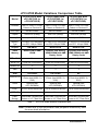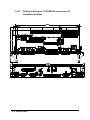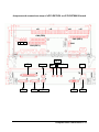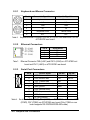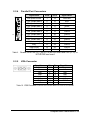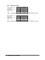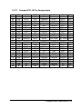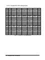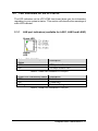
1
NuIPC cPCI-6780 series 6U CompactPCI FSB133 Advanced Function Socket-370 Pentium-III/Celeron CPU Module and Rear I/O Transition Module User’s Guide Recycled Paper Copyright 2001 ADLINK Technology Inc. All Rights Reserved. Manual Rev. 1.00: Feb 19, 2002 Part No. 50-15005-100 The information in this document is subject to change without prior notice in order to improve reliability, design and function and does not represent a commitment on the part of the manufacturer. In no event will the manufacturer be liable for direct, indirect, special, incidental, or consequential damages arising out of the use or inability to use the product or documentation, even if advised of the possibility of such damages. This document contains proprietary information protected by copyright. All rights are reserved. No part of this manual may be reproduced by any mechanical, electronic, or other means in any form without prior written permission of the manufacturer. Trademarks NuIPC is a registered trademark of ADLINK Technology Inc. Other product names mentioned herein are used for identification purposes only and may be trademarks and/or registered trademarks of their respective companies. Getting service from ADLINK • Customer Satisfaction is always the most important thing for ADLINK Technology Inc. If you need any help or service, please contact us and get it. ADLINK Technology Inc. Web Site Sales & Service Technical Support TEL Address http://www.adlinktech.com [email protected] NuDAQ + USBDAQ [email protected] NuDAM [email protected] NuIPC [email protected] NuPRO [email protected] +886-2-82265877 FAX +886-2-82265717 9F, No. 166, Jian Yi Road, Chungho City, Taipei, 235 Taiwan, R.O.C. • Please inform or FAX us of your detailed information for a prompt, satisfactory and constant service. Detailed Company Information Company/Organization Contact Person E-mail Address Address Country TEL Web Site FAX Questions Product Model OS : Computer Environment to Use Challenge Description Suggestions to ADLINK M/B : Chipset : Video Card : Network Interface Card : Other : CPU : BIOS : Table of Contents Chapter 1 Introduction.....................................................1 1.1 Checklist............................................................................ 1 1.1.1 1.1.2 1.2 1.3 1.4 1.5 1.6 Front Board........................................................................... 2 Rear Board ........................................................................... 2 Description ........................................................................ 4 Features ............................................................................ 6 Specifications .................................................................... 7 Functional Block Diagram................................................. 14 Mechanical outline drawing .............................................. 15 1.6.1 1.6.2 Outline drawing for cPCI-6780 series front board......... 15 Outline drawing for cPCI-R6780 series rear I/O transition modules .......................................................... 15 Chapter 2 Jumpers and Connectors.............................17 2.1 Jumpers on the cPCI-6780 and cPCI-R6780 ................... 18 2.1.1 2.1.2 2.2 JP1 on cPCI-6780(TS only)............................................. 22 JP1, 2 , 3 on cPCI-R6780S, R6780SA, R6780V and R6780VA.................................................................... 22 Connectors on the cPCI-6780.......................................... 23 2.2.1 2.2.2 2.2.3 2.2.4 2.2.5 2.2.6 2.2.7 2.2.8 2.2.9 2.2.10 2.2.11 2.2.12 2.2.13 2.2.14 2.2.15 2.2.16 2.2.17 2.2.18 Keyboard and Mouse Connector.................................... 24 Ethernet Connectors ........................................................ 24 Serial Port Connectors ..................................................... 24 Parallel Port Connectors.................................................. 25 VGA Connector................................................................. 25 USB Connectors ............................................................... 26 IDE Connectors (44-pin) .................................................. 27 IDE Connectors (40-pin) .................................................. 28 SCSI Connectors .............................................................. 29 FDD Connector................................................................. 30 AC97 Audio Interface Connectors .................................. 30 Audio Jacks (Optional, with DB-AC97S board) ............ 31 FAN Connector ................................................................. 31 CompactPCI J1 Pin Assignments .................................. 32 CompactPCI J2 Pin Assignments .................................. 33 CompactPCI J3 Pin Assignments .................................. 34 CompactPCI J4 Pin Assignments .................................. 35 CompactPCI J5 Pin Assignments .................................. 36 Table of Contents • i 2.3 LED indicators on the cPCI-6780..................................... 37 2.3.1 2.3.2 2.3.3 2.3.4 2.3.5 LAN port indicators (available for LAN1, LAN2 and LAN3) ........................... 37 IDE Activity LED Indication ............................................. 38 Power LED Indication ...................................................... 38 SCSI Activity LED Indication........................................... 38 SCSI LVD Indication ........................................................ 38 Chapter 3 Getting Start..................................................39 3.1 3.2 3.3 3.4 3.5 CPU Installation ............................................................... 40 Memory Installation.......................................................... 41 CF Installation.................................................................. 42 HDD Installation............................................................... 44 OS installation device connection .................................... 46 3.5.1 3.5.2 3.6 Using cPCI-6780 on ADLINK’s cBP-6108 series backplane.......................................................................... 46 Using cPCI-6780 on other backplanes .......................... 46 Notice for Rear I/O Connection........................................ 47 3.6.1 3.6.2 3.6.3 The I/O implementation is only supported by rear I/O board .................................................................................. 47 The I/O implementation is supported by both rear I/O and front I/O ....................................................................... 47 The FDD and IDE interfaces ........................................... 48 Chapter 4 Driver Installation .........................................50 4.1 Intel 815 Chipset Hardware and VGA Driver..................... 52 4.1.1 4.1.2 4.2 SM721 VGA Drivers Installation (cPCI-6780TS) .............. 56 4.2.1 4.2.2 4.2.3 4.3 Driver Installation on Windows 2000 ............................. 56 Driver Installation on Windows 98.................................. 57 Driver Installation on Windows NT ................................. 58 LAN Drivers Installation.................................................... 59 4.3.1 4.3.2 4.3.3 4.3.4 4.4 Hardware Configuration File Installation ....................... 52 VGA Driver Installation .................................................... 54 Software and Drivers Support ......................................... 59 Driver Installation on Windows 2000 ............................. 60 Driver Installation on Windows 98.................................. 61 Driver Installation on Windows NT ................................. 62 SCSI Drivers Installation.................................................. 63 4.4.1 4.4.2 Software and Drivers Support ......................................... 63 Driver Installation on Windows 2000 ............................. 64 ii • Table of Contents 4.4.3 4.4.4 Driver Installation on Windows 98.................................. 65 Driver Installation on Windows NT ................................. 66 Chapter 5 Watchdog and Utilities .................................68 5.1 Watchdog Timer Configuration......................................... 68 5.1.1 5.1.2 5.2 5.3 5.4 WDT Programming .......................................................... 69 How to Test the WDT? ..................................................... 69 Hardware Doctor Utility .................................................... 70 Intel Preboot Execution Environment (PXE) ..................... 71 PICMG 2.1 Hot Swap Support.......................................... 72 Product Warranty/Service .............................................75 Table of Contents • iii 1 Introduction Thanks for choosing ADLINK’s cPCI-6780 series product. This manual gives you information on the cPCI-6780 series CPU module. The information inside this manual can be applied to all series if without specified. The topics covered in this chapter are as follows: 1.1 • Checklist • Descriptions • Features • Specifications • Functional block diagram • Mechanical outline drawing Checklist The cPCI-6780 series products are compliant with PICMG 2.0 CompactPCI specification with 6U dual-slot form factor. Both front panel I/O and rear panel I/O are supported by cPCI-6780 series products. It is not necessary to use the rear board if the application just requires only front panel I/O wiring or special backplane wiring. The front board (the CPU module) and the rear board (the rear I/O transition module) are sold separately. The standard models cPCI-6780TS, cPCI-6780VS and cPCI-6780V are front boards. And the standard models cPCI-R6780S and cPCI-R6780V are rear boards. Introduction • 1 1.1.1 Front Board Front board is the CPU module. There are three standard versions available for cPCI-6780 series module (please see section 1.2 and the model variations comparison table.) The default version does not included any CPU, RAM or HDD. However, the CPU module may be equipped with different speed or capacity of CPU, RAM, HDD by special request. Please check your configurations with your dealer and check that your package is complete and contains the items below. If you discover damaged or missing items, please contact with your dealer. • The cPCI-6780 CPU module (May be equipped with different speed or capacity of CPU, RAM, HDD. Those items may vary according to the different configuration request) • One CPU cooler (the CPU cooler will be pre-mounted if the module is equipped with CPU by special request) • One 2.5” ATA HDD supporting frame (which is pre-mounted) • One DB-44CFH removable CompactFlash socket adaptor (which is pre-mounted on the 2.5” ATA HDD supporting frame for the standard configuration delivery. The DB-44CFH may not be included if customer request pre-configuring 2.5” ATA HDD/Flash disk or by OEM project request.) • One special designed 2.5” ATA HDD connection cable (which is pre-mounted) • This User’s Manual • ADLINK CD Note: 1. The package of cPCI-6780 OEM version (non-standard configuration, functionality, package or accessories) may vary according to the different configuration request. 2. Please refer to ADLINK All-in-one CD for the BIOS setting instruction manual. User also can download the latest manual from ADLINK website, please visit: www.adlinktech.com 1.1.2 Rear Board Rear board is the rear I/O transition module. Different rear board could provide different functional combination. There are four versions for cPCI-6780 series module, named cPCI-R6780S, R6780SA, R6780V and 2 • Introduction R6780VA. The cPCI-R6780S and cPCI-R6780SA are designed for cPCI-6780TS or cPCI-6780VS. The cPCI-R6780V and cPCI-R6780VA are designed for cPCI-6780V. Please see section 1.2 and the model variations comparison table. Please check your package is complete and contains the items below. If you discover damaged or missing items, please contact with your dealer. • The cPCI-R6780 rear I/O transition module • This User’s Manual • Internal LVD Ultra-2 Wide SCSI cable. (Only in cPCI-R6780S, not available for cPCI-R6780SA, V or VA) Note: The package of cPCI-R6780 OEM version (non-standard configuration, functionality, package or accessories) may vary according to the different configuration request. Introduction • 3 1.2 Description ADLINK cPCI-6780 is a powerful and flexible CompactPCI host slot processor board based on Intel Pentium III processor. This board is specially designed to add performance, memory and bandwidth to ADLINK’s 6U CompactPCI platform for CTI and Telcom applications. It is also suitable for high-reliability embedded applications where performance and a rich feature set are mandatory. cPCI-6780 series are a high performance 6U CompactPCI CPU module powered by Intel FC-PGA and FC-PGA2 Socket-370 Pentium III CPU or Intel Celeron CPU. The CPU module uses the latest Intel i815E chipset which supports processor front side bus (FSB) running at 133MHz and PC-133 DRAM up to 512MB, makes cPCI-6780 performs the best in its peer. Moreover, the Embedded Intel Architecture guarantees the long time availability. The cPCI-6780 series with the rear I/O transition board (cPCI-R6780 series) provide standard I/Os including RS-232/422/485, USB, Printer Port, AGP-VGA, LCD (cPCI-6780TS with cPCI-R6780S), EIDE, SCSI (cPCI-6780VS and cPCI-6780TS with rear board), Triple Ethernets, removable CompactFlash socket and optional AC-97 audio interface. cPCI-6780 is designed to meet the needs of the applications which require high performance and high reliability. It is especially suitable for the broad band data and intelligent network switching, CTI server, semi-conductor equipment, military and medical application. 4 • Introduction cPCI-6780 Model Variations Comparison Table cPCI-6780TS with cPCI-R6780S (or cPCI-R6780SA) cPCI-6780VS with cPCI-R6780S (or cPCI-R6780SA) cPCI-6780V with cPCI-R6780V (or cPCI-R6780VA) Processor Intel FC-PGA/ FC-PGA2 Celeron or Pentium-III Intel FC-PGA/ FC-PGA2 Celeron or Pentium-III Intel FC-PGA/ FC-PGA2 Celeron or Pentium-III CPU FSB 66/100/133MHz 66/100/133MHz 66/100/133MHz Chipset Intel 815E (B-step) Intel 815E (B-step) Intel 815E (B-step) Memory Size up to 512MB up to 512MB up to 512MB Model Memory Type PC100/PC133 Unbuffered PC100/PC133 Unbuffered PC100/PC133 Unbuffered non-ECC 168-pin DIMM non-ECC 168-pin DIMM non-ECC 168-pin DIMM Graphic SMI SM721 Build-in 815E Build-in 815E Video Memory Build-in SM721 4MB VRAM Dynamic host sharing 10MB SDRAM with 4MB Display Cache Dynamic host sharing 10MB SDRAM with 4MB Display Cache TFT-LCD I/F Yes No No Serial Port 4 (one RS-232/422/485) 4 (one RS-232/422/485) 4 (one RS-232/422/485) Parallel Port 2 2 2 USB 4 4 4 SCSI LSI 53C895 LSI 53C895 No 3 Ports (Intel 82559 *2 + ICH2) 3 Ports (Intel 82559 *2 + ICH2) Ethernet Port 3 Ports (Intel 82559 *2 + ICH2) Audio Optional (with cPCI-R6780SA) Optional (with cPCI-R6780SA) Optional (with cPCI-R6780VA) EIDE 4 ATA-33/66/100 devices 4 ATA-33/66/100 devices 4 ATA-33/66/100 devices FDD I/F Yes Yes Yes Flash Storage Removable CompactFlash Removable CompactFlash Removable CompactFlash Socket or 2.5” Flash Drive Socket or 2.5” Flash Drive Socket or 2.5” Flash Drive Table 1: cPCI-6780 model variations comparison table Note: Please refer to the specification and peripheral connectivity table for more detail information. Introduction • 5 1.3 Features • PICMG 2.0 CompactPCI Specification R3.0 Compliant • PICMG 2.1 CompactPCI Hot Swap Specification R2.0 Compliant • Standard 6U form factor, 2-slot (8TE/HP) width • Supports Socket-370 FC-PGA/FC-PGA2 Pentium-III/Celeron CPU running at FSB 66/100/133MHz • Supports up to Socket-370 FC-PGA2 Pentium-III Tualatin CPU • Three 168-pin DIMM socket supports up to 512MB PC-133/PC-100 un-buffered non-ECC SD-RAM • Build-in housing for 2.5” low profile HDD • Supports up to 4 USB ports, 4 serial ports, 2 parallel ports • Supports 7 bus-master PCI devices on CompactPCI bus peripheral slots • On-board high performance AGP 2x VGA display output with dynamic host sharing up to 10MB and 4MB display cache by build-in Intel 815E chipset VGA controller (for model cPCI-6780V/VS series) • On-board high performance AGP 2x VGA/LCD display output by SMI SM721 controller (for model cPCI-6780TS series) • Supports triple 10/100Mb Ethernet ports • Supports Ultra-2 Wide SCSI by LSI SYM53C895 controller (not available for cPCI-6780V) • Supports Intel pre-boot execution environment (PXE) for remote boot • Supports rear I/O configuration • Supports remote console • Supports CompactFlash type-II socket via removable daughter board Note: Please refer to the model variation comparison table for the supported functional features. 6 • Introduction 1.4 Specifications General CompactPCI Features • PCI Rev.2.1 compliant • PICMG 2.0 CompactPCI Rev. 3.0 compliant. • PICMG 2.1 CompactPCI Hot-swap specification Rev.2.0 compliant Form Factor • Standard 6U CompactPCI (front board size: 233.35mm x 160mm, rear board size: 233.35mm x 80mm, not incl. the 2.0mm Hard Metric connectors and the panel with ejectors) • 2-slot (8TE/HP, 40.6mm) wide, incl. housing of 2.5” HDD CPU/Cache • Intel Socket 370 FC-PGA2 Pentium-III (Tualatin) with 512KB on-die L2 cache up to 1.26GHz at 133MHz FSB • Intel Socket 370 FC-PGA Pentium-III with 256KB on-die L2 cache @ full core speed & 100/133MHz FSB • Intel Socket 370 FC-PGA Celeron with 128KB on-die L2 cache @ full core speed & 66/100MHz FSB Note: According to Intel’s spec of FC-PGA and FC-PGA2, the thermal concerns of higher speed CPU, we don’t suggest user to choose the CPU speed higher than the speed limitation on the following environment temperature (the temperature of ventilation air flow): Tair-flow 60 °C 55 °C 50 °C* Max CPU speed/Type 700MHz FC-PGA Pentium-III/Celeron, FSB 100MHz 733MHz FC-PGA Pentium-III, FSB 133MHz 850MHz FC-PGA Pentium-III/Celeron, FSB 100MHz 866MHz FC-PGA Pentium-III, FSB 133MHz 1.26 GHz FC-PGA2 Tualatin, FSB 133 MHz; 1.0 GHz FC-PGA Pentium-III, FSB 133 MHz; 1.2 GHz FC-PGA Celeron, FSB 100 MHz Please refer Intel’s web site http://developer.intel.com for detail information about the processors of Embedded Intel Architecture for applied computing. Introduction • 7 *Must use with special designed thermal module for cPCI-6780 series to achieve the highest operating environment temperature limitation with maximum CPU speed. Chipset • Intel 815E B-stepping with ICH2 BIOS: Award PnP BIOS • BIOS write protection, provide anti-virus capability • On-board Ethernet and SCSI function disable selectable • On-board VGA function disable selectable (only for cPCI-6780TS) • Customized power-on screen (for big quantity OEM project) • DMI BIOS Support: Desktop Management Interface (DMI) allows users to download system hardware-level information such as CPU type, CPU speed, internal/external frequencies and memory size • Green Function: Power management via BIOS, activated through mouse/keyboard movement. • Remote Console: setup console redirection to serial port (terminal mode) with CMOS setup access Host Memory • Three 168-pin DIMM sockets, Max. 512MB un-buffered PC-133 or PC-100 SDRAM IDE Ports • Bus Master IDE controller supports two EIDE interfaces by J3 and J5 rear I/O for up to four IDE devices, including HDD and ATAPI CD-ROM drives. Pin assignments on cPCI J3 and J5 support IDE direct connection feature on cBP-6108 Rev. B1 or later version • One 44-pin Primary EIDE connector on front CPU module, supports on-board 2.5” notebook size HDD or Flash2000TM flash disk • Two 40-pin EIDE connectors on rear transition module supports PIO Mode 3/4 and Ultra DMA/33 IDE devices • One CompactFlash type-II socket on removable transition daughter board for front CPU module On Board Super I/O • Winbond W83627HF and W83627F 8 • Introduction • Supports up to two high-speed bi-directional SPP/EPP/ECP parallel ports with ESD protection to 4KV and downstream device protection to 30V. Primary port is on front CPU module, secondary port on rear transition module • One floppy interface by J3 rear I/O, support two floppy drives (360KB, 720KB, 1.2MB, 1.44MB, 2.88MB.) One 34-pin floppy connector is available on rear I/O transition module • Pin assignments on cPCI J3 support FDD direct connection feature on cBP-6108 Rev. B1 or later version • Two 16C550 UARTs compatible RS-232 COM ports with ESD protection to 2KV on front CPU module • Expandable one 16C550 UARTs compatible RS-232 COM ports with ESD protection to 2KV and one RS-232/422/485/485+ selectable serial port by using of rear transition module USB Interface • Supports up to four USB ports, two ports on front CPU module, the other two ports on rear I/O transition module • USB Specification Rev. 1.1. compliant • Individual over-current protection Watch-dog Timer • Programmable I/O port 2Eh and 2Fh to configure watchdog timer, programmable timer 1~255 seconds or 1~255 minutes • Bundled easy-programming library for DOS, Windows 95, 98, NT Hardware M onitoring • Winbond W83782D built in W83627HF, monitoring temperature, CPU fan, system temperature and DC Voltages CPU On-board VGA Display (available for cPCI-6780V or VS series) • Intel 815E built-in hyper-pipelined architecture 3D graphics engine • AGP 2X, ACPI and VESA compliant • Supports video memory up to 10MB shared with host memory dynamically allocated by driver • On-board 4MB display cache for optimized Intel 815E chipset performance • Supports up to 1600x1200 resolution Introduction • 9 • Supports VGA rear I/O On-board Extend VGA/LCD Display (only available for cPCI-6780TS) • AGP 2x VGA/LCD controller SMI Lynx3DM SM721, with build-in 4M VRAM (8M VRAM available for big quantity OEM project) • VGA display on both front and rear I/O transition module faceplate, 24-bit RGB-TFT LCD connector on rear I/O transition module • High performance, 128-bit, single clock cycle 2D drawing engine • High performance, power managed 3D acceleration engine • AGP 2x, ACPI, VESA DPMS and VESA DDC 2b compliant • Supports up to 1280x1024 VGA display resolution with 24-bit true color, non-interlaced • Optional supports up to 1600x1200 VGA display resolution with 16-bit high color, non-interlaced under Windows NT only. • Dual display and simultaneous display for VGA and LCD • RAMDAC Latch-up protection • Driver supporting: Windows 95/98/ME/NT/2000, Linux, OS/2 Note: 1600x1200 VGA display resolution needs special modified BIOS. This BIOS is only compatible with Windows NT and it might cause incompatibility issues with other OS. On-board Ethernet supporting • Two Ethernet ports on front CPU module featuring by two Intel 82559 Ethernet controllers • One Ethernet port on rear transition module featuring by Intel 815E chipset build-in ICH2 Ethernet controller • IEEE 802.3 10Base-T and 100Base-TX compatible • IEEE 802.3u Auto-negotiation support • IEEE 802.3x 100Base-TX flow control support • Full duplex support at both 10 and 100 Mbps operation On-board SCSI (Feature is available for cPCI-6780VS and TS, rear I/O module is required) • LSI (SYMBIOS) 53C895 Ultra 2 Wide SCSI controller featuring LVD by J4 rear I/O 10 • Introduction Audio Extension (Only for big quantity OEM project) • Single channel AC-97 digital audio interface reserved by J5 rear I/O • Optional AC-97 audio codec daughter board on rear I/O transition module • Supports line-in, line-out and microphone jacks on AC-97 daughter board PCI Bus Bridge • TI PCI2050 transparent PCI to PCI bridge • Supports up to 7 PCI bus mastering devices on CompactPCI bus peripheral slots OS Compatibility • MS-DOS 6.2+, Windows 95/98/ME, Windows NT 4.0, Windows 2000, Red Hat Linux 7.0 and VxWorks Flash Disk Supporting • Support CompactFlash type-II socket on front CPU module by removable transition daughter board • On-board housing for Flash2000TM 2.5” flash disk on front CPU module • Disk-On-Module via 40-pin IDE ports of rear I/O transition module Front Panel LEDs and switch • Power status (green) • IDE activity indicator (amber) • Ethernet port 1&2: 10/100Mb (amber), activity (green) • SCSI activity (amber), LVD/SE indicators (green) • Flush tact switch for system reset Environment • Operating temperature: 0 to 60°C (Note1) • Storage temperature: -20 to 80°C • Humidity: 5% to 95% non-condensed • Shock: 15G peak-to-peak, 11ms duration, non-operation • Vibration: (Note2) ü Non-operation: 1.88Grms, 5-500Hz, each axis Introduction • 11 ü Operation: 0.5Grms, 5-500Hz, each axis, with 2.5” HDD Note: 1. Due to the environment limitations are different from one component to another component, please refer to the component specification when user wish to mount CPU or HDD into cPCI-6780. The operating temperature was tested when the HDD is cabling outside the testing chamber, also with the FC-PGA Socket-370 Pentium-III 700MHz CPU. The operating temperature will be limited by the CPU according to Intel’s CPU spec, not limited by cPCI-6780 card. Please refer to the CPU items in this section. 2. The vibration limitation of operation is caused by 2.5” ATA HDD. If customer will deploy cPCI-6780 into high vibration environment, we suggest user to adopt Flash2000 Flash Disk (FFD series) or CompactFlash Card to replace the usage of 2.5” ATA HDD. Safety Certificate and Test • CE, FCC class B • HALT (temperature and vibration stress) Power Consumption Configurations Pentium III 1.0 GHz 512MB with cPCI-R6780S +5V +3.3V 5.88A 3.76A +12V 270m A -12V 120m A Note: The above values are the measured power consumption for SBC with CPU, CPU cooler and RAM only; the CPU is running under 100% loading. The powers for all the other peripheral devices such as add-on cards, HDD, or CD-ROM are not included. 12 • Introduction Peripheral Connectivity I/O Serial Port (COM1) Serial Port (COM2) Serial Port (COM3) Serial Port (COM4, RS-232/422/485) Parallel Port 1 Parallel Port 2 PS/2 Keyboard PS/2 Mouse Floppy Ultra DMA 33 IDE 1 Ultra DMA 33 IDE 2 USB A/B USB C/D Speaker VGA 24-bit TFT LCD (cPCI-6780TS only) Fast Ethernet Port 1 (Front) Fast Ethernet Port 2 (Front) Fast Ethernet Port 3 (Rear) Ultra 2 wide SCSI (cPCI-6780TS and VS only) LEDs Reset button CompactFlash (via daughter board, optional) AC-97 audio (when using with cPCI-R6780SA and cPCI-R6780VA) Table 2: On-board ------- Rear (Note 1,2) Board ------- Face plate ----Y (J3, DB-9) --- --- --- Y (J3, DB-9) Y (DB-25) --Y (PS/2) Y (PS/2) ------Y ----Y (DB-15) ----------Y (44-pin) ----------- --------Y (J3, 34-pin) Y (J3, 40-pin) Y (J5, 40-pin) ----Y (J3, 2-pin) --- --Y (J3, DB-25) Y (J3, PS/2) Y (J3, PS/2) --------Y (J5) --Y (J5, DB-15) --- --- Y(J2, 44-pin) --- Y (RJ-45) Y (RJ-45) --- ------- ------- ----Y (J5, RJ-45) --- --- Y(J4, HD-68) Y (J4, HD-68) Y Y ----- ----- ----- --- Y (CF-II) --- --- --- --- --- --- Front Face plate Y (DB-9) Y (DB-9) --- Peripheral Connectivity of cPCI-6780 series Note: 1. Please use the proper rear I/O transition module to enable the functions (I/O interfaces) on rear side. The board or system will be damaged if use the improper rear I/O transition module. 2. ADLINK recommends to use cPCI-R6780S (or cPCI-R6780SA) as the rear I/O transition module for cPCI-6780TS and cPCI-6780VS. To use cPCI-R6780V (or cPCI-R6780VA) as the rear I/O transition module for cPCI-6780V. Introduction • 13 1.5 Functional Block Diagram Note 1 ATA-33/66/100 Note 3 Note 2 Note: 1. 2. 3. For cPCI-6780TS, SMI SM721 VGA/LCD controller. For cPCI-6780VS and 6780V, 4MB Display cache. There is no LSI 53C895 on cPCI-6780V. AC97 compliant audio features are available on cPCI-R6780SA and cPCI-R6780VA. 14 • Introduction Mechanical outline drawing 2 R 1 IOIOI 1 2 Outline drawing for cPCI-6780 series front board 2 1.6.1 IOIOI 1.6 Introduction • 15 1.6.2 Outline drawing for cPCI-R6780 series rear I/O transition modules 2 3 IOIOI 4 IOIOI 16 • Introduction 2 Jumpers and Connectors This chapter provides information on how to use the jumpers and connectors on the cPCI-6780 in order to set up a workable system. We also describe the meaning of each LED indicators. The topics covered are: • Jumpers on the cPCI-6780 and cPCI-R6780 • Connectors on the cPCI-6780 and cPCI-R6780 • LED indicators on the cPCI-6780 and cPCI-R6780 Jumpers and Connectors • 17 2.1 Jumpers on the cPCI-6780 and cPCI-R6780 The jumpers on the cPCI-6780 front board or cPCI-R6780 rear board allow you to configure your CPU module according to the needs of your applications. If you have doubts about the best jumper configuration for your needs, contact your dealer or sales representative. The following table lists the jumper connectors on cPCI-6780 or cPCI-R6780 and their respective functions. Board Connector Description cPCI-6780 JP1 Flat Panel Voltage Selection cPCI-R6780 JP1, JP2, JP3 Select COM2 Type Table 3: cPCI-6780 and cPCI-R6780 jumper list Note: There is no jumper for front side bus (FSB) and CPU speed selection. The FSB and CPU speed are set by auto-detection. 18 • Jumpers and Connectors Jumpers and connectors map of cPCI-6780 series board Jumpers and connectors map of cPCI-R6780S/ cPCI-R6780SA board J5 J4 J3 J2 J1 JP1 Battery TI PCI 2050 (Back side) CN5, IDE1 Clear CMOS Push Button SMI SM721 ICH2 LSI 53C895 BIOS Intel 815E North Bridge W83627F Socket-370 W83627HF Intel 82559 LPT USB COM2 Mouse COM1 Intel 82559 LED: LED: IDE ACT SCSI ACT Power SCSI LVD VGA Keyboard LAN1 LAN2 Reset Jumpers and Connectors • 19 Jumpers and connectors map of cPCI-R6780S or cPCI-R6780SA board rJ2 rJ3 rJ4 rJ5 CN2 (FDD) CN5 (IDE 2) JP1 JP2 JP3 CN4 CN3 (IDE 1) Line In LPT 2 COM4 Mouse COM3 Keyboard 20 • Jumpers and Connectors MIC Line Out LAN 3 VGA USB Jumpers and connectors map of cPCI-R6780V or cPCI-R6780VA board rJ2 rJ3 rJ4 rJ5 CN2 (FDD) CN5 (IDE 2) JP1 JP2 JP3 CN4 CN3 (IDE 1) Line In LPT 2 COM4 Mouse COM3 Keyboard MIC Line Out LAN 3 VGA USB Jumpers and Connectors • 21 2.1.1 JP1 on cPCI-6780(TS only) JP1 LCD Power 1-2 +3.3V (Default) 2-3 +5V Table 4: 2.1.2 Setting JP1 LCD Power Setting JP1, 2 , 3 on cPCI-R6780S, R6780SA, R6780V and R6780VA JP1 JP2 JP3 Function 1-3, 1-3, 1-2 2-4 2-4 RS-232 (Default) 3-5, 3-5, 3-4 4-6 4-6 RS-422 3-5, 3-5, 5-6 4-6 4-6 RS-485 Table 5: Setting JP1, 2, 3 Serial Port COM4 Setting 22 • Jumpers and Connectors 2.2 Connectors on the cPCI-6780 The connectors on the cPCI-6780 front board and cPCI-R6780 rear board allows you to connect devices such as keyboard, mouse, printer and internal floppy disk drives, hard disk drives, etc. The following information lists the connectors on cPCI-6780 and cPCI-R6780 and their respective functions. 2.2.1 2.2.2 2.2.3 2.2.4 2.2.5 2.2.6 2.2.7 2.2.8 2.2.9 2.2.10 2.2.11 2.2.12 2.2.13 2.2.14 2.2.15 2.2.16 2.2.17 2.2.18 Keyboard and Mouse Connector ........................................... 24 Ethernet Connectors ................................................................ 24 Serial Port Connectors ............................................................ 24 Parallel Port Connectors ......................................................... 25 VGA Connector ........................................................................ 25 USB Connectors....................................................................... 26 IDE Connectors (44-pin).......................................................... 27 IDE Connectors (40-pin).......................................................... 28 SCSI Connectors...................................................................... 29 FDD Connector......................................................................... 30 AC97 Audio Interface Connectors.......................................... 30 Audio Jacks (Optional, with DB-AC97S board).................... 31 FAN Connector......................................................................... 31 CompactPCI J1 Pin Assignments.......................................... 32 CompactPCI J2 Pin Assignments.......................................... 33 CompactPCI J3 Pin Assignments.......................................... 34 CompactPCI J4 Pin Assignments.......................................... 35 CompactPCI J5 Pin Assignments.......................................... 36 Jumpers and Connectors • 23 2.2.1 Keyboard and Mouse Connector Pin # Table 6: 2.2.2 Down side Signal Name Up side Signal Name 1 Keyboard data Mouse data 2 N.C. N.C. 3 GND GND 4 5V 5V 5 Keyboard Clock Mouse Clock 6 N.C. N.C. Keyboard/Mouse Connector CN3 on cPCI-6780 front board and CN9 on cPCI-R6780 rear board Ethernet Connectors Pin # 1 2 3 6 Signal Name TD+ TDRD+ RD- Table 7: Ethernet Connector CN9 (LAN1) and CN10 (LAN2) on cPCI-6780 front board and CN11 (LAN3) on cPCI-R6780 rear board 2.2.3 Serial Port Connectors Pin # 6 1 5 Table 8: RS-232 Signal RS-422 RS-485 1 DCD, Data carrier detect TX- DATA- 2 RXD, Receive data TX+ DATA+ 3 TXD, Transmit data RX+ 4 DTR, Data terminal ready RX- 5 GND, ground GND 6 DSR, Data set ready 7 RTS, Request to send 8 CTS, Clear to send 9 RI, Ring indicator Serial Ports CN7 (COM1), CN4 (COM2) on cPCI-6780 front board and CN8 (COM3), CN7 (COM4) on cPCI-R7680 rear board (Only COM4 on rear board supports RS-232/RS-422/RS-485 mode.) 24 • Jumpers and Connectors 2.2.4 Parallel Port Connectors 13 14 1 Table 9: 2.2.5 Signal Name Pin # Pin # Signal Name AutoFeed Line printer strobe 1 14 PD0, parallel data 0 2 15 Error PD1, parallel data 1 3 16 Initialize PD2, parallel data 2 4 17 Select PD3, parallel data 3 5 18 Ground PD4, parallel data 4 6 19 Ground PD5, parallel data 5 7 20 Ground PD6, parallel data 6 8 21 Ground PD7, parallel data 7 9 22 Ground ACK, acknowledge 10 23 Ground Busy 11 24 Ground Paper empty 12 25 Ground Select 13 N/A N/A Parallel Ports CN6 (LPT1)on cPCI-6780 front board and CN6 (LPT2) on cPCI-R7680 rear board VGA Connector Signal Name Red Blue GND GND N.C. N.C. HSYNC NC Pin 1 3 5 7 9 11 13 15 Pin 2 4 6 8 10 12 14 Signal Name Green N.C. GND GND GND N.C. VSYNC Table 10: VGA Connector CN2 on cPCI-6780 and CN12 on cPCI-R6780 Jumpers and Connectors • 25 2.2.6 USB Connectors Pin # 1 2 3 4 Signal Name Vcc USBUSB+ Ground Table 11: USB Connector CN1 (Port 1 and Port 2) on cPCI-6780 front board Pin # 1 2 3 4 Signal Name Vcc USBUSB+ Ground Table 12: USB Connector CN11 (Port 3 and Port 4) on cPCI-R6780 rear board 26 • Jumpers and Connectors 2.2.7 IDE Connectors (44-pin) Signal Pin # Pin # Signal RESET- 1 2 Ground DD7 3 4 DD8 DD6 5 6 DD9 DD5 7 8 DD10 DD4 9 10 DD11 DD3 11 12 DD12 DD2 13 14 DD13 DD1 15 16 DD14 DD0 17 18 DD15 Ground 19 20 (keypin) DMARQ 21 22 Ground DIOW- 23 24 Ground DIOR- 25 26 Ground IORDY 27 28 CSEL DMACK- 29 30 Ground INTRQ 31 32 reserved DA1 33 34 PDIAG- DA0 35 36 DA2 CS0- 37 38 CS1- DASP- 39 40 Ground +5V 41 42 +5V Ground 43 44 TYPE- Table 13: Primary IDE channel CN5 on cPCI-6780 front board Jumpers and Connectors • 27 2.2.8 IDE Connectors (40-pin) Signal Pin # Pin # Signal RESET- 1 2 Ground DD7 3 4 DD8 DD6 5 6 DD9 DD5 7 8 DD10 DD4 9 10 DD11 DD3 11 12 DD12 DD2 13 14 DD13 DD1 15 16 DD14 DD0 17 18 DD15 Ground 19 20 (keypin) DMARQ 21 22 Ground DIOW- 23 24 Ground Ground DIOR- 25 26 IORDY 27 28 CSEL DMACK- 29 30 Ground INTRQ 31 32 reserved DA1 33 34 PDIAG- DA0 35 36 DA2 CS0- 37 38 CS1- DASP- 39 40 Ground Table 14: Primary IDE channel CN3 and secondary IDE channel CN5 on cPCI-R6780 rear board 28 • Jumpers and Connectors 2.2.9 SCSI Connectors LVDP12 Signal Pin # 1 Pin # 2 LVDM12 Signal LVDP13 3 4 LVDM13 LVDP14 5 6 LVDM14 LVDP15 7 8 LVDM15 LVDPHP 9 10 LVDPHM LVDP0 11 12 LVDM0 LVDP1 13 14 LVDM1 LVDP2 15 16 LVDM2 LVDP3 17 18 LVDM3 LVDP4 19 20 LVDM4 LVDP5 21 22 LVDM5 LVDP6 23 24 LVDM6 LVDP7 25 26 LVDM7 LVDPLP 27 28 LVDPLM GROUND GROUND 29 30 DFFSENSE 31 32 LVEXT68 LVTRMPWR 33 34 LVTRMPWR LVTRMPWR 35 36 LVTRMPWR N.C. 37 38 N.C. GROUND 39 40 GROUND LVATNP 41 42 LVATNM GROUND 43 44 GROUND LVBSYP 45 46 LVBSYM LVACKP 47 48 LVACKM LVRSTP 49 50 LVRSTM LVMSGP 51 52 LVMSGM LVSELP 53 54 LVSELM LVCDP 55 56 LVCDM LVREQP 57 58 LVREQM LVIOP 59 60 LVIOM LVDP8 61 62 LVDM8 LVDP9 63 64 LVDM9 LVDP10 65 66 LVDM10 LVDP11 67 68 LVDM11 Table 15: SCSI Connectors CN10 and CN13 on cPCI-R6780 Jumpers and Connectors • 29 2.2.10 FDD Connector Signal Pin # Pin # Signal Ground 1 2 DRVDEN0 Ground 3 4 NC NC 5 6 DRVDEN1 Ground 7 8 INDEX# Ground 9 10 MTR0# Ground 11 12 DS1# Ground 13 14 DS0# Ground 15 16 MTR1# Ground 17 18 FDIR# Ground 19 20 STEP# Ground 21 22 WDATA# Ground 23 24 WGATE# Ground 25 26 TRACK0# Ground 27 28 WPT# Ground 29 30 RDATA# Ground 31 32 HDSEL# Ground 33 34 DSKCHG# Table 16: FDD Connector CN2 on cPCI-R6780 2.2.11 AC97 Audio Interface Connectors Pin # 1 2 3 4 5 6 Signal Name Ground AC_BITCLK Ground AC_SDIN0 +5V AC_SDOUT 7 8 9 10 +5V AC_SDIN1 AC_SYNC AC_RESET# Table 17: AC’97 Interface CN4 on cPCI-R6780 for AC’97 daughter board connection 30 • Jumpers and Connectors 2.2.12 Audio Jacks (Optional, with DB-AC97S board) Jack PINK BLUE GREEN Signal Name MIC IN LINE IN LINE OUT Table 18: Audio Jacks on the rear panel (cPCI-R6780SA and cPCI-R6780VA) 2.2.13 FAN Connector 3 1 Pin # 1 2 3 Signal Name Ground +12V Rotation Table 19: FAN Connector CN8 on cPCI-6780 Jumpers and Connectors • 31 2.2.14 CompactPCI J1 Pin Assignments Pin Z A B C D E F 25 GND +5V REQ64# ENUM# +3.3V +5V GND 24 GND AD[1] +5V V(I/O) AD[0] ACK64# GND 23 GND +3.3V AD[4] AD[3] +5V AD[2] GND 22 GND AD[7] GND +3.3V AD[6] AD[5] GND 21 GND +3.3V AD[9] AD[8] GND C/BE[0]# GND 20 GND AD[12] GND V(I/O) AD[11] AD[10] GND 19 GND +3.3V AD[15] AD[14] GND AD[13] GND 18 GND SERR# GND +3.3V PAR C/BE[1]# GND 17 GND +3.3V IPMB_SCL IPMB_SDA GND PERR# GND 16 GND DEVSEL# GND V(I/O) STOP# LOCK# GND 15 GND +3.3V FRAME# IRDY# GND TRDY# GND 11 GND AD[18] AD[17] AD[16] GND C/BE[2]# GND 10 GND AD[21] GND +3.3V AD[20] AD[19] GND 9 GND C/BE[3]# GND AD[23] GND AD[22] GND 8 GND AD[26] GND V(I/O) AD[25] AD[24] GND 7 GND AD[30] AD[29] AD[28] GND AD[27] GND 6 GND REQ# GND +3.3V CLK AD[31] GND 5 GND BRSVP1A5 BRSVP1B5 PCIRST# GND GNT# GND 4 GND IPMB_PWR HEALTHY# V(I/O) INTP INTS GND 3 GND INTA# INTB# INTC# +5V INTD# GND 2 GND TCK +5V TMS TDO TDI GND 1 GND +5V -12V TRST# +12V +5V GND Pin Z A B C D E F 12-14 Key Table 20: CompactPCI J1 pin assignments 32 • Jumpers and Connectors 2.2.15 CompactPCI J2 Pin Assignments 21 20 A GA4 GND (PXI_RSVA22) GND CLK6 GND CLK5 19 GND 18 GND 17 GND 16 GND 15 GND 14 13 12 11 10 9 8 7 6 5 GND GND GND GND GND GND GND GND GND GND Reserved (PXI_TRIG3) Reserved (PXI_TRIG2) Reserved (PXI_TRIG1) Reserved (PXI_BRSVA15) FPVDD(3/5V) FPD12 +12VFP LP FPD11 FPD9 FPD7 FPD4 FPD2 FPD0 4 GND V(I/O) 3 GND 2 GND 1 GND Pin Z CLK4 CLK2 CLK1 A Pin 22 Z GND B C D E F GA3 GA2 GA1 GA0 GND (PXI_RSVB22) (PXI_RSVC22) (PXI_RSVD22) (PXI_RSVE22) GND Reserved Reserved Reserved GND GND Reserved GND Reserved GND Reserved Reserved Reserved GND GND (ICMB_SDA) (ICMB_SCL) (ICMB_PWR) Reserved Reserved Reserved GND GND (PXI_TRIG4) (PXI_TRIG5) (PXI_TRIG6) GND PRST# REQ6# GNT6# GND Reserved (PXI_TRIG0) DEG# GND GND FAL# REQ5# GNT5# GND SHFCLK GND FPVEE(3V) GND FPD13 GND FPD14 GND FPD16 GND Reserved (PXI_BRSVB4) GND CLK3 GND B ENFPVDD V(I/O) FLM V(I/O) FPD15 V(I/O) FPD20 V(I/O) FPD22 V(I/O) GND Reserved GND FPD17 GND FPD10 GND FPD8 GND FPD6 Reserved Reserved M/DE BIASEN ENBKL FPD23 FPD21 FPD19 FPD5 FPD3 GND GND GND GND GND GND GND GND GND GND FPD18 GND FPD1 GND GNT3# SYSEN# REQ1# C REQ4# GNT2# GNT1# D GNT4# REQ3# REQ2# E GND GND GND F Reserved GND (PXI_TRIG7) Table 21: CompactPCI J2 Pin Assignments Jumpers and Connectors • 33 2.2.16 CompactPCI J3 Pin Assignments Pin 19 18 17 16 15 14 13 12 11 10 9 8 7 6 5 4 3 2 1 Pin Z A GND PDRST# GND PDACT# GND PDD15 GND PDD11 GND PDA0 GND PDD7 GND PDD3 GND DS0# GND DS1# GND WRTPRT# GND WGATE# GND PE GND PPD7 GND PPD3 GND Reserved GND Reserved GND CTS3# GND RI4# GND CTS4# Z A B PDCS16# Reserved PDD14 PDD10 PDA1 PDD6 PDD2 DRVDEN1 DSKCHG# HDSEL# ERRORP# SLCTIN# PPD6 PPD2 MSDATA MSCLK RTS3# DTR4# RTS4# B C D E PDIORDY -12V PDIRQ14 PDCS3# PDCS1# PPDIAG PDD13 PDD12 Reserved PDD9 PDD8 PDDACK# +5V PDA2 PDDREQ PDD5 PDD4 PDIOW# PDD1 PDD0 PDIOR# MTR0# INDEX# WDATA# MTR1# DRVDEN0 RDATA# FDIR# TRACK0# STEP# AUTOFD# PBUSY Reserved +5V PSTROB# Reserved PPD5 PPD4 PINIT# PPD1 PPD0 PACK# PCBEEP KBDATA SLCT +5V KBCLK RXD3 DSR3# DCD3# TXD3 RI3# DTR3# RXD4 DSR4# DCD4# TXD4 C D E Table 22: CompactPCI J3 pin assignments 34 • Jumpers and Connectors F GND GND GND GND GND GND GND GND GND GND GND GND GND GND GND GND GND GND GND F 2.2.17 CompactPCI J4 Pin Assignments Pin 25 24 23 22 21 20 19 18 17 16 15 12-14 11 10 9 8 7 6 5 4 3 2 1 Pin Z GND GND GND GND GND GND GND GND GND GND GND A +5V SD14Reserved SD0+ Reserved SD3+ Reserved SD6+ Reserved SEN_EX Reserved B SD12+ +5V SD14+ GND SD0GND SD3GND SD6GND SATN- GND GND GND GND GND GND GND GND GND GND GND Z SACKSMSG+ SMSGSREQ+ SREQSD10+ SD10Reserved Reserved DDCSCL +5V A SACK+ GND GND GND SIOGND SD11Reserved Reserved +5V Reserved B C SD12Reserved SD15+ Reserved SD1Reserved SD4Reserved SD7DIFFSEN SATN+ Key SBSYReserved SSELReserved SIO+ Reserved SD11+ Reserved GREEN DDCSDA HSYNC C D Reserved SD13+ +5V SDP1Reserved SD2GND SD5GND SDP0+5V TERM E +5V SD13SD15SDP1+ SD1+ SD2+ SD4+ SD5+ SD7+ SDP0+ +5V TERM F GND GND GND GND GND GND GND GND GND GND GND GND SRSTGND SCDGND SD9+ GND Reserved +5V VSYNC Reserved D SBSY+ SRST+ SSEL+ SCD+ SD8+ SD8SD9Reserved RED BLUE +5V E GND GND GND GND GND GND GND GND GND GND GND F Table 23: ComapctPCI J4 pin assignments Jumpers and Connectors • 35 2.2.18 CompactPCI J5 Pin Assignments Pin 22 21 20 19 18 17 16 15 14 13 12 11 10 9 8 7 6 5 4 3 2 1 Pin Z GND GND GND GND GND GND GND GND GND GND GND GND GND GND GND GND GND GND GND GND GND GND Z A Reserved Reserved Reserved GND SDD4 SDD12 SDD3 SDD1 SDDREQ SDIORDY SPDIAG SDA0 Reserved AC_SDIN1 OC3# OC2# USBP2LAN_RST Reserved Reserved Reserved Reserved A B Reserved GND GND GND SDD11 GND SDD13 GND SDD14 GND SDCS16# GND SDACT# GND AC_RST# GND USBP2+ GND LAN_TXD2 GND Reserved GND B C Reserved +5V SDD7 SDD9 SDD10 Reserved Reserved Reserved SDD0 Reserved SDDACK# Reserved SDCS3# Reserved AC_SYNC Reserved LAN_RXD1 Reserved LAN_TXD1 Reserved Reserved Reserved C D E Reserved Reserved +5V +5V GND SIDERST# SDD6 SDD8 GND SDD5 Reserved Reserved GND SDD2 Reserved Reserved GND SDD15 SDIOW# SDIOR# GND SDIRQ15 SDA2 SDA1 GND SDCS1# AC_SDOUT AC_BITCLK GND AC_SDIN0 USBP3USBP3+ GND LAN_RXD0 LAN_RXD2 LAN_CLK GND LAN_TXD0 Reserved Reserved Reserved Reserved Reserved Reserved D E Table 24: CompactPCI J5 pin assignments 36 • Jumpers and Connectors F GND GND GND GND GND GND GND GND GND GND GND GND GND GND GND GND GND GND GND GND GND GND F 2.3 LED indicators on the cPCI-6780 The LED indicators on the cPCI-6780 front board show you the information regarding to your system’s status. This section will describe the meanings of each LED indicator. 2.3.1 LAN port indicators (available for LAN1, LAN2 and LAN3) Green LED Amber LED Amber LED 10/100Mbps Description Status OFF 10Mbps transfer rate ON 100Mbps transfer rate Table 25: Green LED indication in LAN port Green LED Link/Activity Status Description OFF No link ON Connecting Blinking Data transfering Table 26: Amber LED indication in LAN port Jumpers and Connectors • 37 2.3.2 IDE Activity LED Indication Yellow LED Description OFF EIDE is not active ON Any one EIDE device is active Table 27: IDE Activity LED indication 2.3.3 Power LED Indication Green LED Description OFF System is not power-on or power failed ON System is power-on Table 28: Power LED indication 2.3.4 SCSI Activity LED Indication Yellow LED Description OFF SCSI bus is not active ON Any one SCSI device is active Table 29: SCSI Activity LED indication Note: Available for cPCI-6780TS and cPCI-6780VS. 2.3.5 SCSI LVD Indication Green LED OFF ON Description Single End SCSI mode Low Voltage Differential SCSI mode Table 30: SCSI LVD indication Note: Available for cPCI-6780TS and cPCI-6780VS. 38 • Jumpers and Connectors 3 Getting Start This chapter provides information on how to install components such as memory, CPU, HDD and CF card on the modules. It also provides notice for choosing the proper components. The topics covered are: • CPU Installation • Memory Installation • CF Installation • HDD Installation • OS installation device connection • Notice for rear I/O connection Getting Start • 39 3.1 CPU Installation The cPCI-6780 CPU module supports Intel Socket 370 FC-PGA or FC-PGA2 Pentium-III processors of 100/133 MHz front side bus (FSB) or Socket 370 FC-PGA Celeron processors of 66/100 MHz FSB. Users need to install high efficient CPU cooler to guarantee the system stability. The factory default cPCI-6780 bare model are not equipped with CPU. User can purchase the off-the-shelf CPU and the related CPU cooler from the market. However, due to the space limitation, the cooler height (including heatsink and fan) cannot over 25mm for FC-PGA package CPU or 23mm for FC-PGA2 package CPU. Please follow the procedure to install CPU and cooler below: 1. Let the CPU socket into “un-lock” status. 2. Insert CPU to the socket by aligning the notch of the CPU with the one of the socket. 3. Let the CPU socket into “lock” status. 4. Mount the CPU cooler carefully. ADLINK’s factory also provides the pre-mounting CPU service for considerable quantities OEM project or customized request. Please contact your dealer or ADLINK’s sales representatives. Note: Ensure that the CPU heat sink and the CPU top surface are in tightly contact to avoid CPU overheating problem that would cause your system to hang or be unstable. The CPU heat sink and fan should be installed tightly too. The FAN with speed sensor is recommend. M Ensure the CPU cooler could provide enough cooling capability for the CPU, otherwise, the CPU or the CPU module will be damaged caused by over-heat. The warranty will be invalid if using the improper CPU cooler. 40 • Getting Start 3.2 Memory Installation The cPCI-6780 CPU module supports three PC-100/PC-133 168-pin DIMM sockets for a maximum total memory of 512MB without ECC support. The memory type must be 3.3V SDRAM. User could choose PC-133 SDRAM to run with FSB 100MHz CPU, but could not choose PC-100 SDRAM to run with FSB 133MHz CPU. Due to the space limitation, the height of RAM modules cannot over 1.15 inches (29.2 mm). It is recommend to use the low profile SDRAM modules approved by ADLINK to ensure the best reliability. The factory default cPCI-6780 bare model are not equipped with RAM modules. The memory module can come with size of 32MB, 64MB, 128MB, 256MB or 512MB PC-100 or PC-133 168-pin SDRAM DIMM. ADLINK’s factory also provides the pre-mounting memory service for considerable quantities OEM project or customized request. Please contact your dealer or ADLINK’s sales representatives. M Ensure that the RAM modules are firmed in the DIMM sockets and not over height limitation, otherwise the components might be damaged when the CPU module is inserting into the chassis. Getting Start • 41 3.3 CF Installation The CompactFlash Disk Card (or called CF storage card) is widely applied on digital consumer devices like PDA, Digital Camera and MP3 player. However, the CF features anti-shock, anti-vibration, better environment tolerance, low power consumption, small form factor and higher reliability, plus standard interface with cost-effectiveness, it has been also widely accepted in the industrial and mission critical embedded application field. In cPCI-6780, it is very easy to use CF card, user can find the CF card socket on the 2.5” ATA HDD supporting frame. The CF card socket adaptor named DB-44CFH is designed for exchange with 2.5” ATA HDD on IDE interface. DB-44CFH supports both type-I and type-II CompactFlash storage device such as CF card or IBM MicroDrive. If user purchases the OEM model or special configuration model, it may not come with DB-44CFH in the package. User can purchase the CF card adaptor (model named: DB-44CFH) as the optional kit to convert the IDE interface to CF card socket. Due to the CF card adaptor utilize the same IDE interface and the same housing that 2.5” ATA HDD might use. So, user should aware to remove 2.5” ATA HDD (if any) first then install the CF card adaptor. Please refer to the section of HDD installation for the instruction of removing 2.5” ATA HDD. DB-44CFH Installation for cPCI-6780 and CF card notice • Mount the CF card adaptor (DB-44CFH) on the 2.5” HDD supporting frame directly by fixing 4 screws • Connect the 44-pin HDD cable which has been special designed, check if pin #1 of the IDE connector, cable and the HDD are matched • Reconfirm the cable, DB-44CFH and HDD supporting frame are fixed • Insert CF card into socket, then check the CF card is fixed enough Note: The CF card on front board utilize Primary EIDE interface (IDE1). Due to the cPCI-6780 front board supports rear I/O, the IDE1 interface is also wiring to rear I/O from CompactPCI connector J3. User have to pay attention that it only supports up to two IDE devices on each EIDE interface, and the master/slave setting should not conflict with each other. Due to the default setting of CF card is setting on master, the IDE1 interface on rear I/O could only apply one IDE device which is set on slave. 42 • Getting Start Removing DB-44CFH from cPCI-6780 • Remove the CF card from the CF socket • Remove the 44-pin HDD cable which connecting DB-44CFH with IDE interface • Remove the CF card adaptor (DB-44CFH) on the 2.5” HDD supporting frame directly by loosing 4 screws Note: There is no necessary to remove 2.5” HDD supporting frame from cPCI-6780 prior then removing DB-44CFH. Getting Start • 43 3.4 HDD Installation In cPCI-6780, user can install one 2.5” ATA HDD or flash drive (e.g. FLASH2000 flash disk, FFD) which is 2.5” ATA HDD form factor. The factory default bare model are equipped with DB-44CFH, the removable CF card adaptor, not equipped with any HDD or FFD. If user want to install 2.5” ATA HDD for larger storage capacity or want to install FFD for more vibration tolerant, user can purchase the off-the-shelf HDD or FFD from the market. However, we recommend to use the product which is approved by ADLINK to ensure the best reliability. Due to the space limitation with better ventilation concern, we recommend to use low profile (or called slim type) 2.5” ATA HDD or FFD that thickness is not over than 9.5mm. Because of the CF card adaptor utilize the same IDE interface and the same housing that 2.5” ATA HDD might use. So, user should aware to remove CF card adaptor (if any) first then install the 2.5” ATA HDD or FFD. Please refer to the section of CF installation for the instruction of removing CF card adaptor. HDD/FFD Installation for cPCI-6780 • Remove the HDD supporting frame by loose the two screws on front panel and loose the three screws at the bottom side (the soldering side; reverse side.) • Lock the HDD on the supporting frame. Please note the orientation of the HDD. The connector must face to the board’s rear side (face to CompactPCI connectors.) • Loosely mount the supporting frame on PCB by three screws • Mount the supporting frame on the front panel by two screws, fix them, then fix the three screws mounted on PCB • Check the master/slave setting on your 2.5” ATA HDD is right • Connect the 44-pin HDD cable which has been special designed, check if pin #1 of the IDE connector, cable and the HDD are matched • Reconfirm the cable, HDD and HDD supporting frame are fixed Note: The 2.5” ATA HDD on front board utilize Primary EIDE interface (IDE1). Due to the cPCI-6780 front board supports rear I/O, the IDE1 interface is also wiring to rear I/O from CompactPCI connector J3. User have to pay attention that it only supports up to two IDE devices on each EIDE interface, and the master/slave setting should not conflict with each other. If user applies one 2.5” ATA HDD on front board and setting on master, the IDE1 interface on rear I/O could only apply one IDE device which is set on slave. 44 • Getting Start Removing HDD/FFD from cPCI-6780 • Remove the 44-pin HDD cable which connecting on the IDE interface • Remove the HDD supporting frame by loose the two screws on front panel and loose the three screws at the bottom side (the soldering side; reverse side.) • Remove the HDD from the supporting frame • Remove the 44-pin HDD cable from the HDD • Loosely mount the supporting frame on PCB by three screws • Mount the supporting frame on the front panel by two screws, fix them, then fix the three screws mounted on PCB Getting Start • 45 3.5 OS installation device connection This section describe how to get start to install the OS into the 6U CompactPCI platform for the cPCI-6780 CPU module. The easiest way to install OS is by connecting ATAPI CD-ROM. 3.5.1 Using cPCI-6780 on ADLINK’s cBP-6108 series backplane Due to cBP-6108 series backplane has the direct connection feature for J3/P3 and J5/P5 rear I/O of IDE interfaces, user can easily connect 40-pin flat cable into IDE interface on the rear side of backplane. Then connect the flat cable into an ATAPI CD-ROM. If user has installed 2.5” ATA HDD or CF card on the front board, it is recommend to connect ATAPI CD-ROM to secondary IDE port on the cBP-6108 series backplane to avoid the possibility of master/slave confliction. 3.5.2 Using cPCI-6780 on other backplanes For the usage of backplanes which are not compatible with the pin assignments for J3/P3 and J5/P5 rear I/O of IDE interfaces of cPCI-6780, user can connect 40-pin flat cable into the IDE interface on cPCI-R6780 series rear board. Then connect the flat cable into an ATAPI CD-ROM. If user has installed 2.5” ATA HDD or CF card on the front board, it is recommend to connect ATAPI CD-ROM to secondary IDE port on the cBP-6108 series backplane to avoid the possibility of master/slave confliction. Note: The 2.5” ATA HDD or CF card on front board utilize Primary EIDE interface (IDE1). Due to the cPCI-6780 front board supports rear I/O, the IDE1 interface is also wiring to rear I/O from CompactPCI connector J3. User have to pay attention that it only supports up to two IDE devices on each EIDE interface, and the master/slave setting should not conflict with each other. Due to almost the default setting of 2.5” ATA HDD or CF card is setting on master, if user want to connect ATAPI CD-ROM to the IDE1 interface on rear I/O, (including the rear I/O port on cBP-6108 backplane and cPCI-R6780 rear board,) please check the master/slave setting does not conflict with the setting of the front board’s HDD or CF card. 46 • Getting Start 3.6 Notice for Rear I/O Connection cPCI-6780 features fully integrated functionality with AGP-VGA display, triple Ethernet ports, 4S2P, 4USB, SCSI, ATA-66/100 IDE, TFT-LCD interface and optional AC-97 audio interface. Some of them are implemented for rear I/O only and some of them are implemented to support both front I/O and rear I/O. This section describes the important notice for using the rear I/O connection. Please refer to Chapter 1 section 1.4 peripheral connectivity for the detailed information of each I/O. 3.6.1 The I/O implementation is only supported by rear I/O board Several I/Os are only supported by rear I/O including COM3, COM4, LPT2, FDD interface, 2 USB, speaker (buzzer), LCD, LAN3, SCSI, TFT-LCD and AC-97 audio. User should apply the proper rear I/O board to get those rear I/O functionality. Please refer to the cPCI-6780 Model Variations Comparison Table in Chapter 1 section 1.2 for the proper front board and rear board combinations. M 1. Please use the proper rear I/O transition module to enable the functions (I/O interfaces) on rear side. The board or system will be damaged if use the improper rear I/O transition module. 2. Due to the TFT-LCD wires to rear I/O via J2, it is compliant with 32-bit CompactPCI system slot pin definitions. Although the pin-definitions for TFT-LCD are safe for 64-bit cPCI backplane, however, it might cause system or board damage to apply cPCI-6780TS with 64-bit cPCI peripheral cards on 64-bit cPCI backplane. 3.6.2 The I/O implementation is supported by both rear I/O and front I/O Several I/Os are supported by rear I/O and front I/O including keyboard, mouse and VGA display. User should apply the proper rear I/O board to get those rear I/O functionality. All cPCI-R6780 series rear boards can support those rear I/O functions. However, user should keep it in mind that those I/Os can be either connected via front or rear side, not both. Getting Start • 47 M 1. Please use the proper rear I/O transition module to enable the functions (I/O interfaces) on rear side. The board or system will be damaged if use the improper rear I/O transition module. 2. Please connect either via front or via rear for one I/O function. Don’t connect one I/O function from both front and rear side at the same time. It will cause I/O device damage or the system module damage and the warranty will be invalid. 3.6.3 The FDD and IDE interfaces If user needs only rear I/O connection of FDD and IDE interfaces, the user can consider apply cPCI-6780 with the backplane support FDD and IDE direct connection features (such as cBP-6108, 6309 or 6402 series backplane) for floppy drive and IDE devices connection. For this kind of application, user does not need to purchase rear board. If user use other backplane which does not support FDD and IDE direct connection, the proper rear I/O board is required. However, user might wish to connect drives from backplane and also use the I/O function on rear I/O board. Please refer the following notices: ♦ For FDD connection: connect FDD cable either via backplane or via rear I/O board, don’t connect both at the same time ♦ For IDE1 connection, when there is no IDE device on front board: user can connect 40-wire IDE cable on both backplane and rear board when the total cable length is not over 45 cm. User should aware the master/slave setting to prevent the setting confliction ♦ For IDE1 connection, when there is one IDE device on front board: user can connect 40-wire IDE cable on either backplane or rear board, not both at the same time. User should aware the master/slave setting to prevent the setting confliction ♦ For IDE2 connection: user can connect 40-wire IDE cable on both backplane and rear board when the total cable length is not over 45 cm. User should aware the master/slave setting to prevent the setting confliction ♦ To connect ATA-66/100 3.5” HDD on rear I/O 40-pin interfaces: • User has to ensure the interface don’t connect with device on the front board • Please use special 80-wire ATA-100 cable to connect 3.5” ATA-66/100 HDD, the cable length should be not over 45 cm 48 • Getting Start • M Connect the wire on either backplane or rear board, do not connect cable on both at the same time Please use the proper rear I/O transition module to enable the functions (I/O interfaces) on rear side. The board or system will be damaged if use the improper rear I/O transition module. Getting Start • 49 4 Driver Installation To install the drivers and utility for the cPCI-6780, please refer the detail installation information from this Chapter. We provide the basic information in this manual, however, for more detail installation information, such as non-Windows OS installation, please refer the extensive explanation inside the ADLINK CD or the correspondent OS installation guide. We put the chip drivers in the following directories: Chipset driver \CHIPDRV\Chipset\I815 On-chip 815E VGA driver \CHIPDRV\VGA\I815 VS) SM721 VGA driver \CHIPDRV\VGA\SM721 (cPCI-6780TS) LAN relative driver \CHIPDRV\LAN\100PDISK LSI 53C895 SCSI driver \CHIPDRV\SCSI\53C895 (cPCI-6780TS, VS) Watchdog relative library \CHIPDRV\WDT Hardware Doctor Utility \Utility\HWDoctor\W8378X (cPCI-6780V, In this users manual, the Bus-mastering IDE driver installation is not described because most of the Windows based OS will install those drivers automatically. 50 • Driver Installation Due to the Windows NT is a none plug-and-play OS, we remind you some tips for installing the Windows NT here: 1. We suggest installing the LAN driver before installing any service pack. 2. We suggest installing the VGA/AGP driver after installing the service pack. Please make sure your service pack do support AGP, service pack 6 or higher is recommend. 3. Once your NT booting procedure is with warning, please check the Event Viewer to make sure what is the really problem. Once the Windows NT is with strange phenomenal which can not be solved, we suggest to re-install the Windows NT service pack, then install the driver in different sequence again. Driver Installation • 51 4.1 Intel 815 Chipset Hardware and VGA Driver This section describes the installation procedure of Intel 815 chipset Device Driver for Windows 95/98/2000. 4.1.1 Hardware Configuration File Installation This section describes system requirements of Intel 815 chipset Device Driver. This driver has been designed for and tested with Windows 98/95. The system must contain a supported Intel processor and chipset configuration. Ensure that a mouse is connected to the system. One of the following versions of Windows 95/98/2000 must be installed on the system prior to running utility program. • Windows 2000 5.00.2195 (Original release) • Windows 98 Second Edition 4.10.2222 (Original Release) • Windows 98 4.10.1998 (Original Release) • Windows 95 4.00.950c (OSR 2.5 with or without USB Supplement) • Windows 95 4.00.950b (OSR 2.1 with USB Supplement) • Windows 95 4.00.950b (OSR 2.1 with USB Supplement) • Windows 95 4.00.950a (OSR1) • Windows 95 4.00.950 (Original Release) Installing Hardware Configuration File This subsection describes how to install the hardware configuration file on a system where Windows 98/95 is installed. Note: Record the location of the Windows 95/98/2000 directory before installing the driver. 1. Check the System Requirements. Windows 95/98/2000 must be fully installed and running on the system prior to running this software. 2. Close any running applications. 52 • Driver Installation 3. The files are stored in an integrated application setup program. This program is designed for a Windows 95/98/2000 program that allows the INF files to be installed. 4. In X:\CHIPDRV\Chipset\I815\Win9x2k\Disk1, SETUP.EXE. 5. Click 'Next' on Welcome Screen to read and agree to the license agreement. Click Yes if you agree to continue. NOTE: If you click No, the program will terminate. 6. Click 'Finish' to restart the system when prompted to do so. 7. Follow the screen instructions and use default settings to complete the setup when Windows 95/98/2000 is re-started. Upon re-start, Windows 95/98/2000 will display that it has found many hardware and is installing driver for them. If one New Hardware Found dialog box is displayed requesting the location of the drivers, use the mouse to click on the scrollbar and click on the <Windows 95/98/2000 directory>. 8. Select Yes, when prompted to re-start Windows 95/98/2000. and then Run Driver Installation • 53 4.1.2 VGA Driver Installation This section provides information on how to install the VGA driver that come in the Compact Disk with the package. Please follow the instructions set forth in this section carefully. Please note that there must be relevant software installed in your system before you could proceed to install the VGA driver. Note: For the driver installation under non-Windows based OS, please refer to the correspondent OS installation guide. Installing the Drivers for Windows 98/95 and Win 2000 The following section describes the normal display driver installation procedures for Windows 95/98/2000. Use the following procedures when installing the display drivers for Windows 98/95. 1. The driver is included in the ADLINK CD. R un the win9xm62.exe (or win2km62.exe for Win2000 installation) under the following directory: X:\CHIPDRV\VGA\I815\w9xme (or W2K folder for Win 2000 installation). 2. Click Next on Welcome Screen to read and agree to the license agreement. 3. Click Yes if you agree to continue. NOTE: If you click No, the program will terminate. 4. Click Yes to restart your computer and for the new settings to take effect. 5. Follow the screen instructions and use default settings to complete the setup when Windows 95/98/2000 is re-started. Installing the Drivers for Windows NT 4.0 [IMPORTANT ]: You should install the Windows NT 4.0 with at least Service Pack 4 (version number: 4.00.1381) first before installing the VGA driver. If you don't have the Windows NT 4.0 Service Pack 4, please contact your software vendor or download it from Microsoft's web site. The procedures below show you how to install the VGA driver for Windows NT 4.0. 1. Boot Windows NT 4.0. 54 • Driver Installation 2. The driver is included in the ADLINK CD. Run the winnt4m62.exe under the following directory: X:\CHIPDRV\VGA\I815\nt40. 3. Click Next on Welcome Screen to read and agree to the license agreement. 4. Click Yes if you agree to continue. NOTE: If you click No, the program will terminate. 5. Windows NT 4.0 will prompt you to restart computer. Click Yes for the new settings to take effect. 6. Follow the screen instructions and use default settings to complete the setup when Windows NT 4.0 is re-started. Driver Installation • 55 4.2 SM721 VGA Drivers Installation (cPCI-6780TS) This chapter describes VGA driver installation for the onboard VGA controller SM721. The relative drivers are in the following ADLINK CD directory: X:\CHIPDRV\VGA\SM721, where X: is the location of the CD-ROM drive. The VGA drivers for Windows 98/95, Windows NT and Windows 2000 are included. Note: For the driver installation under non-Windows based OS, please refer to the correspondent OS installation guide. 4.2.1 Driver Installation on Windows 2000 The Windows 2000 may install the standard VGA driver. We recommend you to manually installed the most updated driver, which shipped with ADLINK CD to guarantee the compatibility. After installing the Windows 2000, please update the new drivers by the following procedures. 1. Boot Windows 2000, Click Start. Select Settings then double-click the Control Panel. 2. Double-click on the System icon, click Hardware tab, click Device Manager button. 3. Double-click either on the Display Adapters or Other Devices entry, Double-click the Video Controller or Silicon Motion Lynx3DM entry. 4. Click on the Driver tab, then click Update Driver… button. 5. An Upgrade Device Driver Wizard windows, click NEXT>. 6. Select Display a list of ... and click NEXT. 7. The next window may show a list of hardware type, then select Display Adapters, then click OK. 8. This window may show a list of VGA model numbers. 9. Insert ADLINK CD and click Have Disk. 10. Browse the SM721 driver in the following path: X:\CHIPDRV\VGA\SM721\WIN2K, highlight smisetup.inf, click OPEN, then click NEXT>. 56 • Driver Installation 11. Highlight the model: Silicon Motion Lynx3DM, then click NEXT>. 12. Click NEXT> button, The Windows 2000 may report Digital Signature Not Found, then click Yes to continue. 13. Click Finish button, then click CLOSE button. 4.2.2 Driver Installation on Windows 98 The Windows 98 may install the standard VGA driver. We recommend you to manually installed the most updated driver, which shipped with ADLINK CD to guarantee the compatibility. After installing Windows 98, please update the new drivers by the following procedures. 1. Boot Windows 98, Click Start. Select Settings then double-click the Control Panel. 2. Double-click System icon, click on the Device Manager tab. 3. Double-click Display Adapters entry, select the Standard PCI Graphics Adapter (VGA) entry. Click the Properties button. 4. Click on the Driver button, then click Update Driver… button. 5. An Upgrade Device Driver Wizard windows, click NEXT>. 6. Select Display a list of ... and click NEXT>. The next window allows the user to specify a specific path. Insert the ADLINK CD and click Have Disk. 7. Browse the SM721 driver in the following path: X:\CHIPDRV\VGA\SM721\WIN9X, highlight smi.inf, click OPEN. Click OK. 8. Click NEXT> button, then the Wizard summary window appears. 9. Click Finish button, then restart the computer to active the new driver. Driver Installation • 57 4.2.3 Driver Installation on Windows NT The Windows NT may install the standard VGA driver while. We recommend you to manually installed the most updated driver, which shipped with ADLINK CD to guarantee the compatibility. After installing Windows NT, please update the new drivers by the following procedures. 1. From the Control Panel, double-click the Display icon. 2. Click the Settings tab, click Display Type…, click Change… button. 3. Insert ADLINK CD and click Have Disk. 4. Browse the SM721 driver in the following path: X:\CHIPDRV\VGA\SM721\NT40, highlight smisetup.inf, click OPEN. Click OK. 5. A windows shows the Display is Silicon Motion Lynx Family, click OK, then click Yes to continue. 6. An Installing Driver window shows successful installing, click OK to continue. 7. Click Close button. 8. Click Close button, then restart the computer to active the new driver. Note: After installing the VGA/AGP drivers, you may find the driver does not work. This may due to you do not install the NT service pack in advance. We suggest installing the NT service pack 4 or higher version to enable APG capability. 58 • Driver Installation 4.3 LAN Drivers Installation This chapter describes LAN driver installation for the onboard Ethernet controller Intel 82559 (LAN1 & LAN2) and Intel PHY 82562 (LAN3, with ICH2 built-in MAC). The relative drivers are under the following ADLINK CD directory: X:\CHIPDRV\LAN\100PDISK, where X: is the location of the CD-ROM drive. Note: For the driver installation under non-Windows based OS, please refer to the correspondent OS installation guide. 4.3.1 Software and Drivers Support The 82559 drivers support the following OS or platforms: • Windows 98, Windows 95, Windows 2000, Windows NT • Novell Netware, DOS Setup for Novell NetWare DOS • UNIX, OS2, Linux All the above drivers are included in the ADLINK CD. In the following section, we will describe the driver installation for Windows 98, Windows 2000, and Windows NT. For the driver installation of the other OS, please refer the readme file inside the CD. Driver Installation • 59 4.3.2 Driver Installation on Windows 2000 The Windows 2000 may install the LAN driver. We recommend you to manually installed the most updated LAN driver, which shipped with ADLINK CD to guarantee the compatibility. After installing the Windows 2000, please update the new drivers by the following procedures. 1. Boot Windows 2000, Click Start. Select Settings then double-click the Control Panel. 2. Double-click System icon, click Hardware tab, click Device Manager button. 3. Double-click Network Adapters entry, Double-click the Intel 8255xbased PCI Ethernet Adapter (10/100) entry. 4. Click Driver tab, then click Update Driver… button. 5. An Upgrade Device Driver Wizard windows, click Next>. 6. Select Display a list of ... and click Next>. The next window may show a list of hardware models. 7. Insert the CD and click Have Disk. 8. Browse the Intel 82559 driver in the following path: X:\CHIPDRV\LAN\100PDISK, highlight oemsetup.inf, click Open, then click OK. 9. Highlight the model: Intel 8255x- based PCI Ethernet Adapter (10/100), then click NEXT>. An Update Driver Warning window may pop up, click Yes to continue. 10. Click NEXT> button, then the Wizard summary window appears. 11. Click Finish button, then click CLOSE button. 60 • Driver Installation 4.3.3 Driver Installation on Windows 98 The Windows 98 will install the LAN driver automatically. We recommend you to manually updated the LAN, which on the ADLINK CD to guarantee the compatibility. After installing Windows 98, please update the new drivers by the following procedures. 1. Boot Windows 98, Click Start. Select Settings then double-click the Control Panel. 2. Double-click on the System icon, click on the Device Manager tab. 3. Either Double-click on the Network Adapters entry, select the Intel 8255x-based PCI Ethernet Adapter (10/100) entry. Click the Properties button. 4. Click on the Driver button, then click Update Driver… button. 5. Update Device Driver Wizard starts, click NEXT. 6. Select Display a list of ... and click NEXT. The next window allows the user to specify a specific path. Insert the CD and click Have Disk. 7. Browse the Intel 82559 driver in the following path: X:\CHIPDRV\LAN\100PDISK, highlight net82557.inf, click OK. The Update Wizard displays the message that it has found the driver. Click OK again to update the driver. Note: Windows 98 may ask you to insert the original Windows 98 CD to install the LAN protocols. 8. Click NEXT button, then the Wizard summary window appears. 9. Click Finish button, then restart the computer to active the new driver. Driver Installation • 61 4.3.4 Driver Installation on Windows NT Before install the LAN driver on Windows NT, please copy the LAN driver in the CD to a floppy diskette. You have to put a new disk into drive A, then type the following batch command under DOS environment to copy the relative NT drivers. X:\CHIPDRV\LAN\100PDISK\Makedisk\Makedisk NT where X is the CD-ROM drive. Windows NT may ask to installs a LAN driver from its own library of drivers. We recommend you to manually updated the LAN, which on the ADLINK CD to guarantee the compatibility. After installing Windows 98, please update the new drivers by the following procedures. 1. From the Control Panel, double-click the Netwrok icon, a Network Configuration window pop up, click Yes. 2. In Netwrok Setup Wizard, click Next>, click Select From List… button. 3. Insert LAN driver floppy diskette into A drive and click Have Disk. 4. In the dialog box of Insert Disk window, type in A:, Click OK. 5. A Select OEM Option window pop up, click OK, then click Next>. 6. Select necessary Network Protocols, click Next>. 7. Select necessary Network Services, click Next>. 8. Click Next> until Window NT Setup dialog box pop up. Type in D:\i386 in the dialog box, then insert the original Windows NT CD, click Continue. 9. Then click OK until the setup completed. 10. Restart the computer to reboot. 62 • Driver Installation 4.4 SCSI Drivers Installation This chapter describes SCSI drivers installation for the onboard SCSI controller LSI (Symbios) 53C895. The relative drivers are under the following ADLINK CD directory: X:\CHIPDRV\SCSI\53C895, where X: is the location of the CD-ROM drive. 4.4.1 Software and Drivers Support The 53C895 drivers support the following OS or platforms: Windows 98, Windows 95, Windows 2000, Windows NT 4.0 DOS, Novell, UNIX, SCO UNIX, OS2, Linux All the above drivers are included in the ADLINK CD. In the following sections, we will describe the driver installation for Windows 98, Windows 2000, and Windows NT. For the driver installation of the other OS, please refer the README file under the respective directory. Note: The most updated SCSI drivers can be downloaded from the LSI Logic web site at URL: http://www.lsilogic.com. Driver Installation • 63 4.4.2 Driver Installation on Windows 2000 The Windows 2000 may install the SCSI driver. We recommend you to manually installed the most updated driver, which shipped with ADLINK CD to guarantee the compatibility. After installing the Windows 2000, please update the new drivers by the following procedures. 1. Boot Windows 2000, Click Start. Select Settings then double-click the Control Panel. 2. Double-click on the System icon, click Hardware tab, click Device Manager button. 3. Double-click SCSI and RAID controllers entry, Double-click Symbios XXX PCI SCSI Adapter entry. 4. Click Driver tab, then click Update Driver… button. 5. An Upgrade Device Driver Wizard window starts, click NEXT> 6. Select Display a list of ..., then click NEXT>. The next window may show a list of hardware models. 7. Insert the ADLINK CD and click Have Disk. 8. Browse the LSI 53C895 driver in the following path: the X:\CHIPDRV\SCSI\53C895\Win2k\winnt\miniport\ Highlight oemsetup.inf, click OPEN, then click NEXT>. 9. Highlight the model: Symbios 8952U PCI SCSI Adapter; 53C895 Device, then click NEXT>. 10. Click NEXT button. The Windows 2000 may report Digital Signature Not Found, then click Yes to continue. 11. Click Finish button, then click CLOSE button. 64 • Driver Installation 4.4.3 Driver Installation on Windows 98 The Windows 98 will automatically install the SCSI drivers. However, we recommend you to manually installed the most updated driver, which shipped with ADLINK CD to guarantee the compatibility. After installing the Windows 98, please update the new drivers by the following procedures. 1. From the Control Panel, double-click System icon, click Device Manager tab. 2. Double-click SCSI Adapters entry, select the Symbios Logic xxxxx SCSI PCI Host Adapter entry. Click the Properties button. 3. Click Driver button, then click Update Driver… button. 4. An Upgrade Device Driver Wizard window pop up, click NEXT>. 5. Select Display a list of ... and click NEXT>. The next window allows the user to specify a specific path. Insert the ADLINK CD and click Have Disk. 6. Browse the 53C895 driver in the following path: X:\CHIPDRV\SCSI\53C895\Win95&98 Highlight symc8xx.inf, click Open, click OK. The previous window appears with the selected driver displayed as the driver to install. 7. Click NEXT> button, then the Wizard summary window appears. 8. Click Finish button, then restart the computer to active the new driver. Driver Installation • 65 4.4.4 Driver Installation on Windows NT Before install the SCSI driver on Windows NT, please copy the contents in the following directory X:\CHIPDRV\SCSI\53C895\Nt40 into a new formatted floppy diskette. Please note that all the content in the sub-directory must be copied too. When install the Windows NT into a SCSI HDD, we recommend you to use IDE CD-ROM as CD reader. Before installing the NT, we have to install the SCSI driver from the floppy diskette you made. Please use the following procedure to install the SCSI driver with Windows NT. 1. Start the Windows NT 4.0 installation by booting from the Windows NT CD or floppy diskettes. 2. Press Enter when the Welcome to Setup screen appears. 3. The Windows NT 4.0 Workstation Setup window appears next. 4. Press S to skip automatic detection and do manual selection. A screen displays the message [Setup has recognized the following mass storage devices in your computer]. 5. Choose S to configure additional SCSI adapters when a screen displays the SCSI adapters found. Move the highlight bar to Other and press Enter. 6. The system prompts for the manufacturer-supplied hardware support disk. Insert the appropriate Symbios Driver diskette, and press Enter. 7. Select Symbios PCI (53C8XX) Driver to be shown highlighted. Press Enter to proceed. 8. The Windows NT Workstation Setup window reappears. If using an IDE CD-ROM for installation, press S to load additional drives. Another window appears. (1) Scroll up and select: IDE CD-ROM (ATAPI 1.2)…., Press Enter. -or(2) Configuring additional SCSI adapters, press Enter. 66 • Driver Installation 9. Upon exiting, a screen displays the message Setup will load support for the following mass storage devices(s). Press Enter to continue. This message implies that Windows NT recognizes the miniport driver and the SCSI hardware. 10. At this point, simply follow the Microsoft Windows NT installation procedure. The Windows NT may already install with a SCSI driver. We recommend you to manually upgrade the driver, which shipped with ADLINK CD to guarantee the compatibility. After installing Windows NT, please update the new drivers by the following procedures. 1. From the Control Panel, double-click the SCSI Adapters icon. 2. Click Drivers tab, click Add… button. 3. Insert the floppy diskette into drive A: and click Have Disk. 4. In Window NT Setup window, type in A: drive in the dialog box, then click Continue button. 5. An Install Driver window shows that the SCSI adapter is Symbios Logic PCI 53C8XX, click OK to continue. 6. An setup successful windows pop up, click OK to continue. 7. Click Close button. 8. Click Close button, then restart the computer to active the new driver. Driver Installation • 67 5 Watchdog and Utilities 5.1 Watchdog Timer Configuration The Watch Dog Timer (WDT) can monitor the system's status. Once you give a value to WDT, the timer will begin to count down. To re-program a new value to WDT, or move keyboard can restart the WDT. If the system is idle or hang, it will reboot when the timer timeout. The function of the watchdog timer is to reset the system automatically. It contains a one-second (or one-minute) resolution down counter (in CRF4 of logical device 8 of super I/O chip) and two Watchdog control registers (CRF2 and CRF3 of logical device 8). We provides the WDT function call for easy use under DOS, Windows 95/98/2000, and Windows NT, please refer the information under X:\CHIPDRV\WDT. 68 • Watchdog and Utilities 5.1.1 WDT Programming In order to simplify the programming code, we provide a sub function for the programmers to implement their software. For DOS, Windows 95 or 98 and Window NT, the sub function format is as follow: out_port (int IOport_number, int Counter_value) IOport_number:0x3F0 -->W83977EF's configuration port. 0x2E -->W83627HF's configuration port. Counter_value: 0 ~ 15300 (255 minutes) (write a zero to disable the timer) Under DOS, Windows 95 or 98 Make a project program with wdt.cpp under Turbo C/C++. Under Windows NT The library installation procedure: (1) run the setup program under NT environment. (2) reboot the system. You can also write your own DLL by referring the DOS source we provide. 5.1.2 How to Test the WDT? Under DOS, Windows 95 or 98 Open a DOS command prompt and execute the following utility on the CD. X: \CHIPDRV\WDT\test <n> /* n = second value. This program can auto detect which Super I/O chip you use. */ Under Windows NT Before you executing the program under NT, you must run the setup program under Windows NT in advance. Open a DOS command prompt window and execute the following command. test977 <n> : n = second value. For W83977EF test627 <n> : n = second value. For W83627HF Watchdog and Utilities • 69 5.2 Hardware Doctor Utility This chapter introduces Hardware Doctor Utility that comes with the CPU board in conjunction with the onboard hardware monitoring function. The section describes the functions of the utility. Hardware Doctor is a self-diagnostic system for PC and must be used with Winbond’s W83781D/W83782D or W83627HF IC series products. It will protect PC Hardware by monitoring several critical items including Power Supply Voltage, CPU Fan speed, and CPU & System temperature. These items are important to the operation of system; errors may result in permanent hurt of PC. Once any item is out of its normal range, an obvious warning message will pop up and remind user to make a proper treatment. The Hardware Doctor utility supports the Windows 98 and Windows NT. The software is stored on the ADLINK CD under the following directory: X:\Utility\HWDoctor\W8378X\WIN98 and X:\Utility\HWDoctor\W8378X\NT4. Please install the Hardware Doctor by executing the HI2C-98.exe or HI2C-NT.exe respectively under Windows 98 or Windows NT. For detail user's manual, please refer the HWDoctor.PDF under the X:\Utility\HWDoctor\W8378X\. 70 • Watchdog and Utilities 5.3 Intel Preboot Execution Environment (PXE) cPCI-6780 series support Intel Preboot Execution Environment (PXE) which provides the capability of boot-up from Ethernet even executing OS installation from Ethernet. There should be a DHCP server in the network with one or more servers running PXE service and MTFTP service. It could be a Windows NT or Windows 2000 server running DHCP, PXE and MTFTP service or a dedicated DHCP server with one or more additional server running PXE and MTFTP service. The section describes the major items for building up a network environment with PXE support. 1. Setup a DHCP server with PXE tag configuration. 2. Install the PXE and MTFTP services. 3. Make boot image file on PXE server (that is the boot server). 4. Enable the PXE boot function on the client computer. For more detailed information, please refer to pdkrel30.pdf under the directory X:\Utility\PXE_PDK. Watchdog and Utilities • 71 5.4 PICMG 2.1 Hot Swap Support The cPCI-6780 Hot-Swap capability allows non-system slot boards to be added or removed while the system is powered up. Individual clocks for each slot and access to the ENUM# signal on the backplane are compatible to PICMG 2.1 Hot Swap Specification. While hot swap of non-system boards is supported, the cPCI-6780 itself cannot be inserted to or removed from a powered system. A signal (ENUM#) is provided to notify the cPCI-6780 that either a board has been freshly inserted or is about to be extracted. This signal drives a BIOS-programmed interrupt (IRQ9) to inform the cPCI-6780 that the configuration of the system has changed. The cPCI-6780 then performs any necessary maintenance such as installing a device driver upon board insertion, or quiescing a device driver and the board, prior to the board’s extraction. The CompactPCI Hot-Plug System Driver manages the ENUM# sensing. Hot Swap Software builds on the PCI Hot-Plug architecture. The Hot-Plug Service, Hot-Plug System Driver, and the Device Drivers are common elements with the Hot-Plug architecture. The Device Drivers for Hot-Swap boards must be Hot-Plug capable. The Hot-Plug Service provides for the Dynamic Configuration of the system as the resources are added or removed. These services are defined by the PCI Hot-Plug Specification. To support Hot Swap capability, the peripheral board shall be fully compliant with PICMG 2.0 R3.0 and PICMG 2.1 R2.0. The board insertion and extraction processes are summarized as follows. Insertion process: 1. The peripheral board is not installed 2. The physical connection process begins. 3. The operator picks a peripheral board in order to install it in the system. 4. The peripheral board enters the card guide. 5. The peripheral board front panel is discharged to chassis ground through a bleed resistor. 72 • Watchdog and Utilities 6. The peripheral board logic ground is discharged to chassis ground through a bleed resistor. 7. The bleed resistor breaks contact with chassis ground. Logic ground is again isolated. 8. The front panel makes low resistance contact with chassis ground through the card guide. 9. The peripheral board contacts long pins on backplane, and begins to contact ground, +5V, +3V, and V(I/O) pins. 10. The peripheral board is in an unstable state while pins are first mated. This duration can potentially be infinite if the board is just marginally connecting the longest pins. 11. Enough pins are connected that a stable early power can be achieved. Hardware puts the Hot Swap (blue) LED on the peripheral board to the ON state. 12. The peripheral board contacts the medium length pins on the backplane. The peripheral board is now receiving the PCI clock. 13. The peripheral board contacts the short BD_SEL# pin. This pin is grounded on the backplane and pulled high by a pull-up resistor on the peripheral board. Its assertion indicates that the peripheral board has been fully inserted into the backplane. Extraction Process: 1. The peripheral board is installed. 2. The operator starts to withdraw the peripheral board. 3. The BD_SEL# pin disconnects. The hardware connection layer turns on the blue LED if it hasn’t been turned on by software. 4. Medium length CompactPCI pins disengage. Watchdog and Utilities • 73 5. Long length CompactPCI pins disengage. Early power goes away. The peripheral board is in an unstable state while pins are first disconnecting. This duration can potentially be infinite if the board is just marginally connecting the longest pins. 6. Board logic ground is connected to chassis ground through a bleed resistor. 7. The board front panel is connected to chassis ground through a bleed resistor. 8. Board leaves the ESD card guide. 8. The board is not installed. If it is not necessary to support Hot Swap Capability, user could disable the function in BIOS setting and release IRQ9 for other resource. Please refer to cPCI-6780 BIOS manual for operational instruction. 74 • Watchdog and Utilities Product Warranty/Service ADLINK warrants that equipment furnished will be free from defects in material and workmanship for a period of one year from the date of shipment. During the warranty period, we shall, at our option, either repair or replace any product that proves to be defective under normal operation. This warranty shall not apply to equipment that has been previously repaired or altered outside our plant in any way as to, in the judgment of the manufacturer, affect its reliability. Nor will it apply if the equipment has been used in a manner exceeding its specifications or if the serial number has been removed. ADLINK does not assume any liability for consequential damages as a result from our product uses, and in any event our liability shall not exceed the original selling price of the equipment. The remedies provided herein are the customer’s sole and exclusive remedies. In no event shall ADLINK be liable for direct, indirect, special or consequential damages whether based on contract of any other legal theory. The equipment must be returned postage-prepaid. Package it securely and insure it. You will be charged for parts and labor if the warranty period is expired or the product is proves to be misuse, abuse or unauthorized repair or modification. Product Warranty/Service • 75