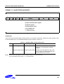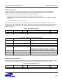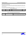
1
KS32C50100 RISC MICROCONTROLLER
1
PRODUCT OVERVIEW
PRODUCT OVERVIEW
OVERVIEW
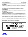
Samsung's KS32C50100 16/32-bit RISC microcontroller is a cost-effective, high-performance microcontroller
solution for Ethernet-based systems. An integrated Ethernet controller, the KS32C50100, is designed for use in
managed communication hubs and routers.
The KS32C50100 is built around an outstanding CPU core: the 16/32-bit ARM7TDMI RISC processor designed by
Advanced RISC Machines, Ltd. The ARM7TDMI core is a low-power, general purpose microprocessor macro-cell
that was developed for use in application-specific and custom-specific integrated circuits. Its simple, elegant, and
fully static design is particularly suitable for cost-sensitive and power-sensitive applications.
The KS32C50100 offers a configurable 8-Kbyte unified cache/SRAM and Ethernet controller which reduces total
system cost. Most of the on-chip function blocks have been designed using an HDL synthesizer and the
KS32C50100 has been fully verified in Samsung's state-of-the-art ASIC test environment.
Important peripheral functions include two HDLC channels with buffer descriptor, two UART channels, 2-channel
GDMA, two 32-bit timers, and 18 programmable I/O ports. On-board logic includes an interrupt controller, DRAM/
SDRAM controller, and a controller for ROM/SRAM and flash memory. The System Manager includes an internal
32-bit system bus arbiter and an external memory controller.
The following integrated on-chip functions are described in detail in this user's manual:
•
8-Kbyte unified cache/SRAM
•
I2C interface
•
Ethernet controller
•
HDLC
•
GDMA
•
UART
•
Timers
•
Programmable I/O ports
•
Interrupt controller
1-1
PRODUCT OVERVIEW
KS32C50100 RISC MICROCONTROLLER
FEATURES
Architecture
•
Integrated system for embedded ethernet
applications
•
Data alignment logic
•
Endian translation
•
100/10-Mbit per second operation
•
Fully 16/32-bit RISC architecture
•
Full compliance with IEEE standard 802.3
•
Little/Big-Endian mode supported basically, the
internal architecture is big-endian.
So, the little-endian mode only support for
external memory.
•
MII and 7-wire 10-Mbps interface
•
Station management signaling
•
On-chip CAM (up to 21 destination addresses)
•
Efficient and powerful ARM7TDMI core
•
Full-duplex mode with PAUSE feature
•
Cost-effective JTAG-based debug solution
•
Long/short packet modes
•
Boundary scan
•
PAD generation
System Manager
HDLCs
•
8/16/32-bit external bus support for ROM/SRAM,
flash memory, DRAM, and external I/O
•
•
One external bus master with bus request/
acknowledge pins
•
Support for EDO/normal or SDRAM
•
Programmable access cycle (0–7 wait cycles)
•
Four-word depth write buffer
•
Cost-effective memory-to-peripheral DMA
interface
HDLC protocol features:
–
Flag detection and synchronization
–
Zero insertion and deletion
–
Idle detection and transmission
–
FCS generation and detection (16-bit)
–
Abort detection and transmission
•
Address search mode (expandable to 4 bytes)
•
Selectable CRC or No CRC mode
•
Automatic CRC generator preset
Unified Instruction/Data Cache
•
Digital PLL block for clock recovery
•
Two-way, set-associative, unified 8-Kbyte cache
•
Baud rate generator
•
Support for LRU (least recently used) protocol
•
NRZ/NRZI/FM/Manchester data formats for Tx/Rx
•
Cache is configurable as an internal SRAM
•
Loop-back and auto-echo modes
•
Tx/Rx FIFOs have 8-word (8 × 32-bit) depth
•
Selectable 1-word or 4-word data transfer mode
I2C Serial Interface
•
Master mode operation only
•
Data alignment logic
•
Baud rate generator for serial clock generation
•
Endian translation
•
Programmable interrupts
•
Modem interface
Ethernet Controller
•
DMA engine with burst mode
•
Up to 10 Mbps operation
•
DMA Tx/Rx buffers (256 bytes Tx, 256 bytes Rx)
•
HDLC frame length based on octets
•
MAC Tx/Rx FIFO buffers (80 bytes Tx, 16 bytes
Rx)
•
2-channel DMA buffer descriptor for Tx/Rx on
each HDLC
1-2
KS32C50100 RISC MICROCONTROLLER
DMA Controller
•
2-channel General DMA for memory-to-memory,
memory-to-UART, UART-to-memory data
transfers without CPU intervention
PRODUCT OVERVIEW
•
Pins individually configurable to input, output, or
I/O mode for dedicated signals
Interrupt Controller
•
Initiated by a software or external DMA request
•
•
Increments or decrements a source or destination
address in 8-bit, 16-bit or 32-bit data transfers
21 interrupt sources, including 4 external interrupt
sources
•
Normal or fast interrupt mode (IRQ, FIQ)
4-data burst mode
•
Prioritized interrupt handling
•
UARTs
PLL
•
Two UART (serial I/O) blocks with DMA-based or
interrupt-based operation
•
The external clock can be multiplied by on-chip
PLL to provide high frequency system clock
•
Support for 5-bit, 6-bit, 7-bit, or 8-bit serial data
transmit and receive
•
The input frequency range is 10-40MHz
•
The output frequency is 5 times of input clock. To
get 50MHz, input clock frequency should be
10MHz.
•
Programmable baud rates
•
1 or 2 stop bits
•
Odd or even parity
•
Break generation and detection
•
Parity, overrun, and framing error detection
•
×16 clock mode
•
Infra-red (IR) Tx/Rx support (IrDA)
Timers
•
Two programmable 32-bit timers
•
Interval mode or toggle mode operation
Operating Voltage Range
•
3.3 V ± 5 %
Operating Temperature Range
•
0 °C to + 70 °C
Operating Frequency
•
Up to 50 MHz
Package Type
Programmable I/O
•
•
208 pin QFP
18 programmable I/O ports
1-3
PRODUCT OVERVIEW
KS32C50100 RISC MICROCONTROLLER
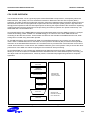
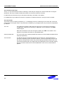
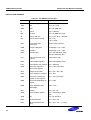
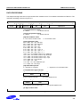
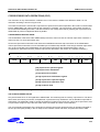
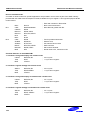
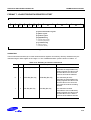
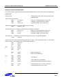
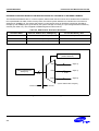
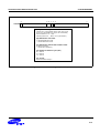
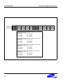
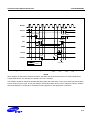
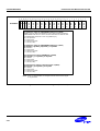
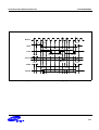
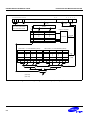
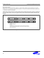
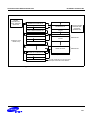
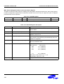
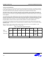
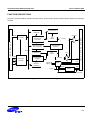
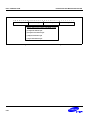
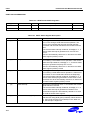
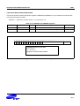
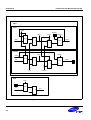
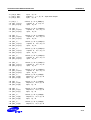
ARM7TDMI
32-Bit RISC CPU
CPU Interface
8-Kbyte
Unified
Cache
4-Word
Write
Buffer
Bus Router
SCL
SDA
18 I/O Ports including
4: Ext INT req,
2: Timer out (0, 1),
2: Ext DMA REQ,
2: Ext DMA ACK
Console
6-Bank
ROM
SRAM
FLASH
32-Bit
System
Bus
System
Bus
Arbiter
4-Bank
External
I/O
Device
Ext. Bus
REQ/ACK
2-Channel HDLCs
with DMAs
External
Bus
Master
Remote
Port A, B
Ethernet Controller
18 General I/O Ports
2-Channel BDMA
Interrupt Controller
BDMA RAMs
Tx Buffer (256 Bytes)
Rx Buffer (256 Bytes)
CAM (128 Bytes)
UART 0, 1
GDMA 0, 1
PLL
MAC
Tx FIFO (80 Bytes)
Rx FIFO (16 Bytes)
TAP Controller for JTAG
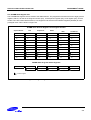
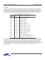
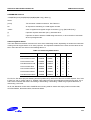
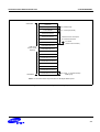
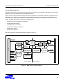
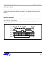
Figure 1-1 KS32C50100 Block Diagram
1-4
4-Bank
DRAM
Memory
Controller
with
Refresh
Control
I 2C
32-Bit Timer 0, 1
Xtal
Osc
ICEBreaker
MII or
7-wire
PRODUCT OVERVIEW
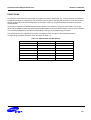
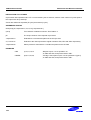
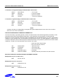
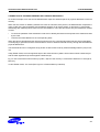
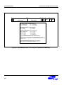
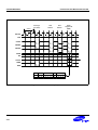
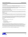
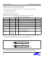
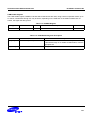
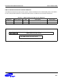
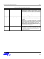
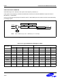
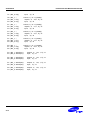
208
207
206
205
204
203
202
201
200
199
198
197
196
195
194
193
192
191
190
189
188
187
186
185
184
183
182
181
180
179
178
177
176
175
174
173
172
171
170
169
168
167
166
165
164
163
162
161
160
159
158
157
VSS
VDD
UARXD1
nUADSR0
UATXD0
nUADTR0
UARXD0
SDA
SCL
P<17>/TOUT1
VSS
VDD
P<16>/TOUT0
P<15>/nXDACK<1>
P<14>/nXDACK<0>
P<13>/nXDREQ<1>
P<12>/nXDREQ<0>
P<11>/xINREQ<3>
P<10>/xINREQ<2>
P<9>/xINREQ<1>
VSS
VDD
P<8>/xINREQ<0>
P<7>
P<6>
P<5>
P<4>
P<3>
P<2>
P<1>
VSS
VDD
P<0>
XDATA<31>
XDATA<30>
XDATA<29>
XDATA<28>
XDATA<27>
XDATA<26>
XDATA<25>
VSS
VDD
XDATA<24>
XDATA<23>
XDATA<22>
XDATA<21>
XDATA<20>
XDATA<19>
XDATA<18>
XDATA<17>
VSS
VDD
KS32C50100 RISC MICROCONTROLLER
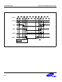
KS32C50100
208-QFP
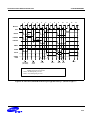
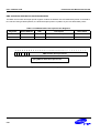
156
155
154
153
152
151
150
149
148
147
146
145
144
143
142
141
140
139
138
137
136
135
134
133
132
131
130
129
128
127
126
125
124
123
122
121
120
119
118
117
116
115
114
113
112
111
110
109
108
107
106
105
VSS
VDD
XDATA<16>
XDATA<15>
XDATA<14>
XDATA<13>
XDATA<12>
XDATA<11>
XDATA<10>
XDATA<9>
XDATA<8>
XDATA<7>
XDATA<6>
VSS
VDD
XDATA<5>
XDATA<4>
XDATA<3>
XDATA<2>
XDATA<1>
XDATA<0>
ADDR<21>
ADDR<20>
ADDR<19>
ADDR<18>
VSS
VDD
ADDR<17>
ADDR<16>
ADDR<15>
ADDR<14>
ADDR<13>
ADDR<12>
ADDR<11>
ADDR<10>/AP
ADDR<9>
ADDR<8>
VSS
VDD
ADDR<7>
ADDR<6>
ADDR<5>
ADDR<4>
ADDR<3>
ADDR<2>
ADDR<1>
ADDR<0>
ExtMACK
ExtMREQ
nWBE<3>/DQM<3>
VSS
VDD
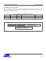
53
54
55
56
57
58
59
60
61
62
63
64
65
66
67
68
69
70
71
72
73
74
75
76
77
78
79
80
81
82
83
84
85
86
87
88
89
90
91
92
93
94
95
96
97
98
99
100
101
102
103
104
1
2
3
4
5
6
7
8
9
10
11
12
13
14
15
16
17
18
19
20
21
22
23
24
25
26
27
28
29
30
31
32
33
34
35
36
37
38
39
40
41
42
43
44
45
46
47
48
49
50
51
52
VDDa
VSSa
FILTER
VDD
VSS
TCK
TMS
TDI
TD0
nTRST
TMODE
UCLK
VDD
VSS
nECS<0>
nECS<1>
nECS<2>
nECS<3>
nEWAIT
nOE
BOSIZE<0>
BOSIZE<1>
nRCS<0>
CLKOEN
SDCLK/MCLKO
VDD
VSS
XCLK
VSS
nRESET
CLKSEL
nRCS<1>
nRCS<2>
nRCS<3>
nRCS<4>
nRCS<5>
nSDCS<0>/nRAS<0>
nSDCS<1>/nRAS<1>
nSDCS<2>/nRAS<2>
VDD
VSS
nSDCS<3>/nRAS<3>
nSDRAS/nCAS<0>
nSDCAS/nCAS<1>
CKE/nCAS<2>
nCAS<3>
nDWE
DQM0/nWBE<0>
DQM1/nWBE<1>
DQM2/nWBE<2>
VDD
VSS
VDD
VSS
nUADTR1
UATXD1
nUADSR1
nDTRA
RXDA
nRTSA
TXDA
nCTSA
VDD
VSS
nDCDA
RXCA
nSYNCA
TXCA
nDTRB
RTDB
nRTSB
TXDB
VDD
VSS
nCTSB
nDCDB
RXCB
nSYNCB
TXCB
CRS/CRS_10M
RX_DV/LINK_10M
RXD<0>/RXD_10M
VDD
VSS
RXD<1>
RXD<2>
RXD<3>
RX_ERR
RX_CLK/RXCLK_10K
COL/COL_10M
TXD<0>/TXD_10M
TXD<1>/LOOP_10M
VDD
VSS
TXD<2>
TXD<3>
TX_ERR/PCOMP_10M
TX_CLK/TXCLK_10M
TX_EN/TXEN_10M
MDIO
LITTLE
MDC
VDD
VSS
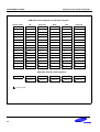
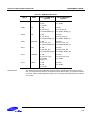
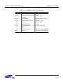
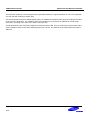
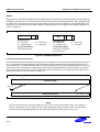
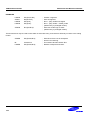
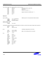
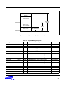
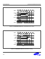
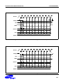
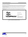
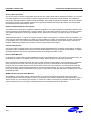
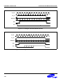
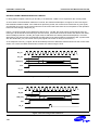
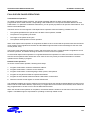
Figure 1-2 KS32C50100 Pin Assignment Diagram
1-5
PRODUCT OVERVIEW
KS32C50100 RISC MICROCONTROLLER
SIGNAL DESCRIPTIONS
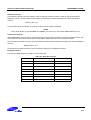
Table 1-1 KS32C50100 Signal Descriptions
Signal
Pin No.
Type
Description
XCLK
80
I
KS32C50100 System Clock source. If CLKSEL is Low, PLL output
clock is used as the KS32C50100 internal system clock. If CLKSEL
is High, XCLK is used as the KS32C50100 internal system clock.
MCLKO/SDCLK (1)
77
O
System Clock Out. MCLKO is monitored as the same phase of
internal system clock, MCLK.
SDCLK is system clock for SDRAM
CLKSEL
83
I
Clock Select. When CLKSEL is '0'(low level), PLL output clock can
be used as the master clock. When CLKSEL is '1'(high level), the
XCLK is used as the master clock.
nRESET
82
I
Not Reset. nRESET is the global reset input for the KS32C50100.
TO allow a system reset, and for internal digital filtering, nRESET
must be held to Low level for at least 64 master clock cycles. Refer
to "Figure 3. KS32C50100 reset timing diagram" for more details
about reset timing.
CLKOEN
76
I
Clock Out Enable/Disable. (See the pin description for MCLKO.)
TMODE
63
I
Test Mode. The TMODE bit settings are interpreted as follows:
'0' = normal operating mode, '1' = chip test mode.
This TMODE pin also can be used to change MF of PLL.
To get 5 times internal system clock from external clock, '0'(low
level) should be assigned to TMODE. If '1'(high level), MF will be
changed to 6.6.
FILTER
55
AI
If the PLL is used, 820pF capacitor should be connected between
the pin and analog groud.
TCK
58
I
JTAG Test Clock. The JTAG test clock shifts state information and
test data into, and out of, the KS32C50100 during JTAG test
operations. This pin is internally connected pull-down.
TMS
59
I
JTAG Test Mode Select. This pin controls JTAG test operations in
the KS32C50100. This pin is internally connected pull-up.
TDI
60
I
JTAG Test Data In. The TDI level is used to serially shift test data
and instructions into the KS32C50100 during JTAG test operations.
This pin is internally connected pull-up.
TDO
61
O
JTAG Test Data Out. The TDO level is used to serially shift test data
and instructions out of the KS32C50100 during JTAG test
operations.
nTRST
62
I
JTAG Not Reset. Asynchronous reset of the JTAG logic.
This pin is internally connected pull-up.
1-6
KS32C50100 RISC MICROCONTROLLER
PRODUCT OVERVIEW
Table 1-1 KS32C50100 Signal Descriptions
Signal
Pin No.
Type
Description
ADDR[21:0]/
ADDR[10]/AP (1)
117–110,
129–120,
135–132
O
Address Bus. The 22-bit address bus, ADDR[21:0], covers the full
4M word address range of each ROM/SRAM, flash memory,
DRAM, and the external I/O banks.
The 23-bit internal address bus used to generate DRAM address.
The number of column address bits in DRAM bank can be
programmed 8bits to 11bits use by DRAMCON registers.
ADDR[10]/AP is the auto precharge control pin. The auto precharge
command is issued at the same time as burst read or burst write
by asserting high on ADDR[10]/AP.
XDATA[31:0]
141–136,
154–144,
166–159,
175–169
I/O
External (bi-directional, 32-bit) Data Bus. The KS32C50100 data
bus supports external 8-bit, 16-bit, and 32-bit bus sizes.
nRAS[3:0]/
nSDCS[3:0] (1)
94, 91, 90,
89
O
Not Row Address Strobe for DRAM. The KS32C50100 supports up
to four DRAM banks. One nRAS output is provided for each bank.
nSDCS[3:0] are chip select pins for SDRAM.
nCAS[3:0]
nCAS[0]/nSDRAS
nCAS[1]/nSDCAS
98, 97, 96,
95
O
Not column address strobe for DRAM. The four nCAS outputs
indicate the byte selections whenenver a DRAM bank is accessed.
nSDRAS is row address strobe signal for SDRAM. Latches row
addresses on the positive going edge of the SDCLK with nSDRAS
low. Enable row access and precharge. nSDCAS is column address
strobe for SDRAM. Latches column addresses on the positive going
edge of the SDCLK with nSDCAS low. Enables column access.
CKE is clock enable signal for SDRAM. Masks SDRAM system
clock, SDCLK to freeze operation from the next clock cycle.
SDCLK should be enabled at least one cycle prior to new
command. Disable input buffers of SDRAM for power down in
standby.
99
O
DRAM Not Write Enable. This pin is provided for DRAM bank write
operations. (nWBE[3:0] is used for write operations to the ROM/
SRAM/flash memory banks.) .
70, 69, 68,
67
O
Not External I/O Chip Select. Four external I/O banks are provided
for external memory-mapped I/O operations. Each I/O bank stores
up to 16 Kbytes. nECS signals indicate which of the four external
I/O banks is selected.
71
I
Not External Wait. This signal is activated when an external I/O
device or ROM/SRAM/flash bank 5 needs more access cycles than
those defined in the corresponding control register.
88–84, 75
O
Not ROM/SRAM/Flash Chip Select. The KS32C50100 can access
up to six external ROM/SRAM/Flash banks. By controlling the
nRCS signals, you can map CPU addresses into the physical
memory banks.
74, 73
I
Bank 0 Data Bus Access Size. Bank 0 is used for the boot program.
You use these pins to set the size of the bank 0 data bus as follows:
'01' = one byte, '10' = half-word, '11' = one word, and '00' =
reserved.
nCAS[2]/CKE (1)
nDWE
nECS[3:0]
nEWAIT
nRCS[5:0]
B0SIZE[1:0]
1-7
PRODUCT OVERVIEW
KS32C50100 RISC MICROCONTROLLER
Table 1-1 KS32C50100 Signal Descriptions
Signal
Pin No.
Type
72
O
Not Output Enable. Whenever a memory access occurs, the nOE
output controls the output enable port of the specific memory
device.
107,
102–100
O
Not Write Byte Enable. Whenever a memory write access occurs,
the nWBE output controls the write enable port of the specific
memory device (except for DRAM). For DRAM banks, CAS[3:0]
and nDWE are used for the write operation.
DQM is data input/output mask signal for SDRAM.
ExtMREQ
108
I
External Bus Master Request. An external bus master uses this pin
to request the external bus. When it activates the ExtMREQ signal,
the KS32C50100 drives the state of external bus pins to high
impedance. This lets the external bus master take control of the
external bus. When it has the control, the external bus master
assumes responsibility for DRAM refresh operations. The
ExtMREQ signal is deactivated when the external bus master
releases the external bus. When this occurs, ExtMACK goes Low
level and the KS32C50100 assumes the control of the bus.
ExtMACK
109
O
External Bus Acknowledge. (See the ExtMREQ pin description.)
MDC
50
O
Management Data Clock. The signal level at the MDC pin is used
as a timing reference for data transfers that are controlled by the
MDIO signal.
MDIO
48
I/O
Management Data I/O. When a read command is being executed,
data that is clocked out of the PHY is presented on this pin. When a
write command is being executed, data that is clocked out of the
controller is presented on this pin for the Physical Layer Entity, PHY.
LITTLE
49
I
Little endian mode select pin. If LITTLE is High, KS32C50100
operate in little endian mode. If Low, then in Big endian mode.
Default value is low because this pin is pull-downed internally.
COL/COL_10M
38
I
Collision Detected/Collision Detected for 10M. COL is asserted
asynchronously with minimum delay from the start of a collision on
the medium in MII mode. COL_10M is asserted when a 10-Mbit/s
PHY detects a collision.
TX_CLK/
TXCLK_10M
46
I
Transmit Clock/Transmit Clock for 10M. The controller drives
TXD[3:0] and TX_EN from the rising edge of TX_CLK. In MII mode,
the PHY samples TXD[3:0] and TX_EN on the rising edge of
TX_CLK. For data transfers, TXCLK_10M is provided by the 10Mbit/s PHY.
TXD[3:0]
LOOP_10M
TXD_10M
44, 43,
40,
39
O
Transmit Data/Transmit Data for 10 M/Loop-back for 10M. Transmit
data is aligned on nibble boundaries. TXD[0] corresponds to the
first bit to be transmitted on the physical medium, which is the LSB
of the first byte and the fifth bit of that byte during the next clock.
TXD_10M is shared with TXD[0] and is a data line for transmitting to
the 10-Mbit/s PHY. LOOP_10M is shared with TXD[1] and is driven
by the loop-back bit in the control register.
nOE
nWBE[3:0]/
DQM[3:0] (1)
1-8
Description
KS32C50100 RISC MICROCONTROLLER
PRODUCT OVERVIEW
Table 1-1 KS32C50100 Signal Descriptions
Signal
Pin No.
Type
Description
TX_EN/
TXEN_10M
47
O
Transmit Enable/Transmit Enable for 10M. TX_EN provides precise
framing for the data carried on TXD[3:0]. This pin is active during
the clock periods in which TXD[3:0] contains valid data to be
transmitted from the preamble stage through CRC. When the
controller is ready to transfer data, it asserts TXEN_10M.
TX_ERR/
PCOMP_10M
45
O
Transmit Error/Packet Compression Enable for 10M. TX_ERR is
driven synchronously to TX_CLK and sampled continuously by the
Physical Layer Entity, PHY. If asserted for one or more TX_CLK
periods, TX_ERR causes the PHY to emit one or more symbols
which are not part of the valid data, or delimiter set located
somewhere in the frame that is being transmitted. PCOMP_10M is
asserted immediately after the packet’s DA field is received.
PCOMP_10M is used with the Management Bus of the DP83950
Repeater Interface Controller (from National Semiconductor). The
MAC can be programmed to assert PCOMP if there is a CAM
match, or if there is not a match. The RIC (Repeater Interface
Controller) uses this signal to compress (shorten) the packet
received for management purposes and to reduce memory usage.
(See the DP83950 Data Sheet, published by National
Semiconductor, for details on the RIC Management Bus.)
This pin is controlled by a special register, with which you can
define the polarity and assertion method (CAM match active or not
match active) of the PCOMP signal.
CRS/CRS_10M
28
I
Carrier Sense/Carrier Sense for 10M. CRS is asserted
asynchronously with minimum delay from the detection of a nonidle medium in MII mode. CRS_10M is asserted when a 10-Mbit/s
PHY has data to transfer. A 10-Mbit/s transmission also uses this
signal.
RX_CLK/
RXCLK_10M
37
I
Receive Clock/Receive Clock for 10M. RX_CLK is a continuous
clock signal. Its frequency is 25 MHz for 100-Mbit/s operation, and
2.5 MHz for 10-Mbit/s. RXD[3:0], RX_DV, and RX_ERR are driven
by the PHY off the falling edge of RX_CLK, and sampled on the
rising edge of RX_CLK. To receive data, the TXCLK_10 M clock
comes from the 10-Mbit/s PHY.
35, 34, 33,
30
I
Receive Data/Receive Data for 10M. RXD is aligned on nibble
boundaries. RXD[0] corresponds to the first bit received on the
physical medium, which is the LSB of the byte in one clock period
and the fifth bit of that byte in the next clock. RXD_10M is shared
with RXD[0] and it is a line for receiving data from the 10-Mbit/s
PHY.
RXD[3:0]/
RXD_10M
1-9
PRODUCT OVERVIEW
KS32C50100 RISC MICROCONTROLLER
Table 1-1 KS32C50100 Signal Descriptions
Signal
Pin No.
Type
Description
RX_DV/LINK_10M
29
I
Receive Data Valid/Link Status for 10M. PHY asserts RX_DV
synchronously, holding it active during the clock periods in which
RXD[3:0] contains valid data received. PHY asserts RX_DV no later
than the clock period when it places the first nibble of the start
frame delimiter (SFD) on RXD[3:0]. If PHY asserts RX_DV prior to
the first nibble of the SFD, then RXD[3:0] carries valid preamble
symbols. LINK_10M is shared with RX_DV and used to convey the
link status of the 10-Mbit/s endec. The value is stored in a status
register.
RX_ERR
36
I
Receive Error. PHY asserts RX_ERR synchronously whenever it
detects a physical medium error (e.g., a coding violation). PHY
asserts RX_ERR only when it asserts RX_DV.
TXDA
9
O
HDLC Ch-A Transmit Data. The serial output data from the
transmitter is coded in NRZ/NRZI/FM/Manchester data format.
RXDA
7
I
HDLC Ch-A Receive Data. The serial input data received by the
device should be coded in NRZ/NRZI/FM/Manchester data format.
The data rate should not exceed the rate of the KS32C50100
internal master clock.
nDTRA
6
O
HDLC Ch-A Data Terminal Ready. nDTRA output indicates that the
data terminal device is ready for transmission and reception.
nRTSA
8
O
HDLC Ch-A Request To Send. The nRTSA output goes low when
there is exist data to be sent in TxFIFO. The data to be sent is
transmitted the nCTS is active state.
nCTSA
10
I
HDLC Ch-A Clear To Send. The KS32C50100 stores each
transition of nCTS to ensure that its occurrence would be
acknowledged by the system.
nDCDA
13
I
HDLC Ch-A Data Carrier Detected. A High level on this pin resets
and inhibits the receiver register. Data from a previous frame that
may remain in the RxFIFO is retained. The KS32C50100 stores
each transition of nDCD.
nSYNCA
15
O
HDLC Ch-A Sync is detected. This indicates the reception of a flag.
The nSYNC output goes low for one bit time beginning at the last bit
of the flag.
RXCA
14
I
HDLC Ch-A Receiver Clock. When this clock input is used as the
receiver clock, the receiver samples the data on the positive edge
of RXCA clock. This clock can be the source clock of the receiver,
the baud rate generator, or the DPLL.
TXCA
16
I/O
HDLC Ch-A Transmitter Clock. When this clock input is used as the
transmitter clock, the transmitter shifts data on the negative
transition of the TXCA clock . If you do not use TXCA as the
transmitter clock, you can use it as an output pin for monitoring
internal clocks such as the transmitter clock, receiver clock, and
baud rate generator output clocks.
TXDB
20
O
HDLC Ch-B Transmit Data. See the TXDA pin description.
RXDB
18
I
HDLC Ch-B Receive Data. See the RXDA pin description.
1-10
KS32C50100 RISC MICROCONTROLLER
PRODUCT OVERVIEW
Table 1-1 KS32C50100 Signal Descriptions
Signal
Pin No.
Type
Description
nDTRB
17
O
HDLC Ch-B Data Terminal Ready. See the nDTRA pin description.
nRTSB
19
O
HDLC Ch-B Request To Send. See the nRTSA pin description.
nCTSB
23
I
HDLC Ch-B Clear To Send. See the nCTSA pin description.
nDCDB
24
I
HDLC Ch-B Data Carrier Detected. See the nDCDA pin description.
nSYNCB
26
O
HDLC Ch-B Sync is detected. See the nSYNCA pin description.
RXCB
25
I
HDLC Ch-B Receiver Clock. See the RXCA pin description.
TXCB
27
I/O
UCLK
64
I
The external UART clock input. MCLK or PLL generated clock can
be used as the UART clock. You can use UCLK, with an appropriate
divided by factor, if a very precious baud rate clock is required.
UARXD0
202
I
UART0 Receive Data. RXD0 is the UART 0 input signal for
receiving serial data.
UATXD0
204
O
UART0 Transmit Data. TXD0 is the UART 0 output signal for
transmitting serial data.
nUADTR0
203
I
Not UART0 Data Terminal Ready. This input signals the
KS32C50100 that the peripheral (or host) is ready to transmit or
receive serial data.
nUADSR0
205
O
Not UART0 Data Set Ready. This output signals the host (or
peripheral) that UART 0 is ready to transmit or receive serial data.
UARXD1
206
I
UART1 Receive Data. See the RXD0 pin description.
UATXD1
4
O
UART1 Transmit Data. See the TXD0 pin description.
nUADTR1
3
I
Not UART1 Data Terminal Ready. See the DTR0 pin description.
nUADSR1
5
O
Not UART1 Data Set Ready. See the DSR0 pin description.
P[7:0]
185–179,
176
I/O
General I/O ports. See the I/O ports, chapter 12.
XINTREQ[3:0]
P[11:8]
191–189,
186
I/O
External interrupt request lines or general I/O ports.
See the I/O ports, chapter 12.
nXDREQ[1:0]/
P[13:12]
193, 192
I/O
Not External DMA requests for GDMA or general I/O ports.
See the I/O ports, chapter 12.
HDLC Ch-B Transmitter Clock. See the TXCA pin description.
nXDACK[1:0]
P[15:14]
195, 194
I/O
Not External DMA acknowledge from GDMA or general I/O ports.
See the I/O ports, chapter 12.
TOUT0/P[16]
196
I/O
Timer 0 out or general I/O port. See the I/O ports, chapter 12.
TOUT1/P[17]
199
I/O
Timer 1 out or general I/O port. See the I/O ports, chapter 12.
SCL
200
I/O
I2C serial clock.
SDA
201
I/O
I2C serial data.
1-11
PRODUCT OVERVIEW
KS32C50100 RISC MICROCONTROLLER
Table 1-1 KS32C50100 Signal Descriptions
Signal
Pin No.
Type
Description
VDDP
1, 21, 41,
56, 78, 92,
105, 118,
130, 155,
167, 177,
197
Power
I/O pad power
VDDI
11, 31, 51,
65, 103,
142, 157,
187, 207
Power
Internal core power
VSSP
2, 22, 42,
57, 79, 81,
93, 106,
119, 131,
156, 168,
178, 198
GND
I/O pad ground
VSSI
12, 32, 52,
66, 104,
143, 158,
188, 208
GND
Internal core ground
VDDA
53
Power
VSSA/VBBA
54
GND
Analog power for PLL
Analog/Bulk ground for PLL
NOTES:
1. SDRAM or EDO/normal DRAM interface signal pins are shared functions. It’s functions will be configured by SYSCFG[31].
1-12
KS32C50100 RISC MICROCONTROLLER
PRODUCT OVERVIEW
Table 1-2 KS32C50100 Pin List and PAD Type
Group
System
Configuration
(8)
TAP Control
(5)
Memory
Interface
(83)
Pin Name
Pin
Counts
I/O
Type
Pad Type
Description
XCLK
1
I
ptic
KS32C50100 system source clock.
MCLKO
1
O
pob4
System clock out.
CLKSEL
1
I
ptic
Clock select.
nRESET
1
I
ptis
Not reset.
CLKOEN
1
I
ptic
Clock out enable/disable.
TMODE
1
I
ptic
Test mode.
LITTLE
1
I
pticd
Little endian mode select pin
FILTER
1
I
pia_bb
PLL filter pin
TCK
1
I
ptic
JTAG test clock.
TMS
1
I
pticu
JTAG test mode select.
TDI
1
I
pticu
JTAG test data in.
TDO
1
O
ptot2
JTAG test data out.
nTRST
1
I
pticu
JTAG not reset.
ADDR[21:0]
22
O
ptot6
Address bus.
XDATA[31:0]
32
I/O
ptbsut6
External, bi-directional, 32-bit data bus.
nRAS[3:0]
4
O
pot4
Not row address strobe for DRAM.
nCAS[3:0]
4
O
pot4
Not column address strobe for DRAM.
nDWE
1
O
pot4
Not write enable
nECS[3:0]
4
O
pot4
Not external I/O chip select.
nEWAIT
1
I
ptic
Not external wait signal.
nRCS[5:0]
6
O
pot4
Not ROM/SRAM/flash chip select.
B0SIZE[1:0]
2
I
ptic
Bank 0 data bus access size.
nOE
1
O
pot4
Not output enable.
nWBE[3:0]
4
O
pot4
Not write byte enable.
ExtMREQ
1
I
ptic
External master bus request.
ExtMACK
1
O
pob1
External bus acknowledge.
1-13
PRODUCT OVERVIEW
KS32C50100 RISC MICROCONTROLLER
Table 1-2 KS32C50100 Pin List and PAD Type
Group
Ethernet
Controller
(18)
HDLC
Channel A
(9)
1-14
Pin Name
Pin
Counts
I/O
Type
Pad Type
Description
MDC
1
O
pob4
Management data clock.
MDIO
1
I/O
ptbcut4
Management data I/O.
COL/
COL_10M
1
I
ptis
Collision detected/collision detected for 10M.
TX_CLK/
TXCLK_10M
1
I
ptis
Transmit data/transmit data for 10M.
TXD[3:0]/
TXD_10M/
LOOP_10M
4
O
pob4
Transmit data/transmit data for 10M.
TX_EN/
TXEN_10M
1
O
pob4
Transmit enable or transmit enable for 10M.
TX_ERR/
PCOMP_10M
1
O
pob4
Transmit error/packet compression enable for
10M.
CRS/
CRS_10M
1
I
ptis
Carrier sense/carrier sense for 10M.
RX_CLK/
RXCLK_10M
1
I
ptis
Receive clock/receive clock for 10M.
RXD[3:0]/
RXD_10M
4
I
ptis
Receive data/receive data for 10M.
RX_DV/
LINK_10M
1
I
ptis
Receive data valid.
RX_ERR
1
I
ptis
Receive error.
TXDA
1
O
pob4
HDLC channel A transmit data.
RXDA
1
I
ptis
HDLC channel A receive data.
nDTRA
1
O
pob4
HDLC channel A data terminal ready.
nRTSA
1
O
pob4
HDLC channel A request to send.
nCTSA
1
I
ptis
HDLC channel A clear to send.
nDCDA
1
I
ptis
HDLC channel A data carrier detected.
nSYNCA
1
O
pob4
HDLC channel A sync is detected.
RXCA
1
I
ptis
HDLC channel A receiver clock.
TXCA
1
I/O
ptbsut1
HDLC channel A transmitter clock.
KS32C50100 RISC MICROCONTROLLER
PRODUCT OVERVIEW
Table 1-2 KS32C50100 Pin List and PAD Type
Group
HDLC
Channel B
(9)
UART 0
(5)
UART 1
(4)
GeneralPurpose
I/O Ports,
( xINTREQ,
nXDREQ,
nXDACK,
Timer 0, 1 )
(18)
I2C
(2)
Pin Name
Pin
Counts
I/O
Type
Pad Type
Description
TXDB
1
O
pob4
HDLC channel B transmit data.
RXDB
1
I
ptis
HDLC channel B receive data.
nDTRB
1
O
pob4
HDLC channel B data terminal ready.
nRTSB
1
O
pob4
HDLC channel B request to send.
nCTSB
1
I
ptis
HDLC channel B clear to send.
nDCDB
1
I
ptis
HDLC channel B data carrier detected.
nSYNCB
1
O
pob4
HDLC channel B sync is detected.
RXCB
1
I
ptis
HDLC channel B receiver clock.
TXCB
1
I/O
ptbsut1
HDLC channel B transmitter clock.
UCLK
1
I
ptis
UART External Clock for UART0/UART1
UARXD0
1
I
ptic
UART 0 receive data.
UATXD0
1
O
pob4
UART 0 transmit data.
nUADTR0
1
I
ptic
Not UART 0 data terminal ready.
nUADSR0
1
O
pob4
Not UART0 data set ready.
UARXD1
1
I
ptic
UART 1 receive data.
UATXD1
1
O
pob4
UART 1 transmit data.
nUADTR1
1
I
ptic
Not UART 1 data terminal ready.
nUADSR1
1
O
pob4
Not UART 1 data set ready.
P[7:0]
8
I/O
ptbst4sm
General I/O ports.
xINTREQ[3:0]
/P[11:8]
4
I/O
ptbst4sm
External interrupt requests or general I/O ports.
nXDREQ[1:0]/
P[13:12]
2
I/O
ptbst4sm
External DMA requests for GDMA or general
I/O ports.
nXDACK[1:0]/
P[15:14]
2
I/O
ptbst4sm
External DMA acknowledge from GDMA or
general I/O ports.
TIMER0/P[16]
1
I/O
ptbst4sm
Timer 0 out or general I/O port.
TIMER1/P[17]
1
I/O
ptbst4sm
Timer 1 out or general I/O port.
SCL
1
I/O
ptbcd4
I2C serial clock.
SDA
1
I/O
ptbcd4
I2C serial data.
1-15
PRODUCT OVERVIEW
Pad
Type
KS32C50100 RISC MICROCONTROLLER
I/O
Type
Table 1-3 KS32C50100 PAD Type
Current
Cell Type
Drive
Feature
Slew-Rate
Control
ptic
I
–
LVCMOS Level
5V-tolerant
–
ptis
I
–
LVCMOS Schmit
Trigger Level
5V-tolerant
–
pticu
I
–
LVCMOS Level
5V-tolerant
Pull-up register
–
pticd
I
–
LVCMOS Level
5V-tolerant
Pull-down register
–
pia_bb
I
–
Analog input with
seperate bulk bias
–
–
pob1
O
1mA
Normal Buffer
–
–
ptot2
O
2mA
Tri-state Buffer
5V-tolerant
–
pob4
O
4mA
Normal Buffer
–
–
ptot4
O
4mA
Tri-state Buffer
5V-tolerant
–
ptot6
O
6mA
Tri-state Buffer
5V-tolerant
–
ptbsut1
I/O
1mA
LVCMOS Schmit trigger
level Tri-state Buffer
5V-tolerant
Pull-up register
–
ptbcut4
I/O
4mA
LVCMOS Level
Tri-state Buffer
5V-tolerant
Medium
ptbcd4
I/O
4mA
LVCMOS Level
Open drain Buffer
5V-tolerant
–
NOTE: 1. pticu and pticd provides 100K Ohm Pull-up(down) register.
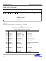
For detail information about the pad type, see Chapter 4. Input/Output Cells of the "STD90/MDL90 0.35um 3.3V
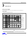
Standard Cell Library Data Book", produced by Samsung Electronics Co., Ltd, ASIC Team .
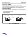
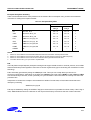
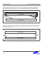
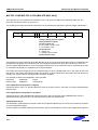
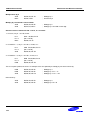
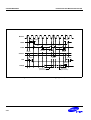
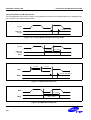
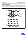
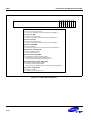
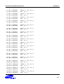
nRESET
64*f MCLK
512*f MCLK
nRCS0
NOTE:
After the falling edge of nRESET, the KS32C50100 count 64 cycles for a
sysetem reset and needs further 512 cycles for a TAG RAM clear of cache.
After these cycles, the KS32C50100 asserts nRCS0 when the nRESET is
released.
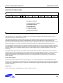
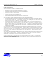
Figure 1-3 Reset Timing Diagramt
1-16
KS32C50100 RISC MICROCONTROLLER
PRODUCT OVERVIEW
CPU CORE OVERVIEW
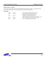
The KS32C50100 CPU core is a general purpose 32-bit ARM7TDMI microprocessor, developed by Advanced
RISC Machines, Ltd. (ARM). The core architecture is based on Reduced Instruction Set Computer (RISC)
principles. The RISC architecture makes the instruction set and its related decoding mechanism simpler and more
efficient than those with microprogrammed Complex Instruction Set Computer (CISC) systems. High instruction
throughput and impressive real-time interrupt response are among the major beneifts of the architecture. Pipelining
is also employed so that all components of the processing and memory systems can operate continuously. The
ARM7TDMI has a 32-bit address bus.
An important feature of the ARM7TDMI processor that makes itself distinct from the ARM7 processor is a unique
architectural strategy called THUMB. The THUMB strategy is an extension of the basic ARM architecture
consisting of 36 instruction formats. These formats are based on the standard 32-bit ARM instruction set, while
having been re-coded using 16-bit wide opcodes.
As THUMB instructions are one-half the bit width of normal ARM instructions, they produce very high-density
codes. When a THUMB instruction is executed, its 16-bit opcode is decoded by the processor into its equivalent
instruction in the standard ARM instruction set. The ARM core then processes the 16-bit instruction as it would a
normal 32-bit instruction. In other words, the THUMB architecture gives 16-bit systems a way to access the 32-bit
performance of the ARM core without requiring the full overhead of 32-bit processing.
As the ARM7TDMI core can execute both standard 32-bit ARM instructions and 16-bit THUMB instructions, it
allows you to mix the routines of THUMB instructions and ARM code in the same address space. In this way, you
can adjust code size and performance, routine by routine, to find the best programming solution for a specific
application.
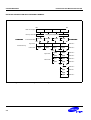
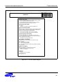
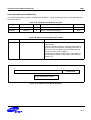
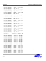
ADDRESS
REGISTER
ADDRESS
INCREMENTER
REGISTER BANK
INSTRUCTION
DECODER and
LOGIC CONTROL
MULTIPLIER
BARREL
SHIFTER
32-BIT ALU
INSTRUCTION
PIPELINE and READ
DATA REGISTER
WRITE DATA
REGISTER
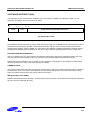
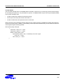
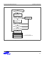
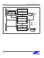
Figure 1-4 ARM7TDMI Core Block Diagram
1-17
PRODUCT OVERVIEW
KS32C50100 RISC MICROCONTROLLER
INSTRUCTION SET
The KS32C50100 instruction set is divided into two subsets: a standard 32-bit ARM instruction set and a 16-bit
THUMB instruction set.
The 32-bit ARM instruction set is comprised of thirteen basic instruction types, which can, in turn, be divided into
four broad classes:
•
Four types of branch instructions which control program execution flow, instruction privilege levels, and
switching between an ARM code and a THUMB code.
•
Three types of data processing instructions which use the on-chip ALU, barrel shifter, and multiplier to
perform high-speed data operations in a bank of 31 registers (all with 32-bit register widths).
•
Three types of load and store instructions which control data transfer between memory locations and the
registers. One type is optimized for flexible addressing, another for rapid context switching, and the third for
swapping data.
•
Three types of co-processor instructions which are dedicated to controlling external co-processors. These
instructions extend the off-chip functionality of the instruction set in an open and uniform way.
NOTE
All 32-bit ARM instructions can be executed conditionally.
The 16-bit THUMB instruction set contains 36 instruction formats drawn from the standard 32-bit ARM instruction
set. The THUMB instructions can be divided into four functional groups:
•
Four branch instructions.
•
Twelve data processing instructions, which are a subset of the standard ARM data processing instructions.
•
Eight load and store register instructions.
•
Four load and store multiple instructions.
NOTE
Each 16-bit THUMB instruction has a corresponding 32-bit ARM instruction with an identical
processing model.
The 32-bit ARM instruction set and the 16-bit THUMB instruction set are good targets for compilers of many
different high-level languages. When an assembly code is required for critical code segments, the ARM
programming technique is straightforward, unlike that of some RISC processors which depend on sophisticated
compiler technology to manage complicated instruction interdependencies.
Pipelining is employed so that all parts of the processor and memory systems can operate continuously. Typically,
while one instruction is being executed, its successor is being decoded, and the third instruction is being fetched
from memory.
1-18
KS32C50100 RISC MICROCONTROLLER
PRODUCT OVERVIEW
MEMORY INTERFACE
The CPU memory interface has been designed to help the highest performance potential to be realized without
incurring high costs in the memory system. Speed-critical control signals are pipelined so that system control
functions can be implemented in standard low-power logic. These pipelined control signals allow you to fully exploit
the fast local access modes, offered by industry standard dynamic RAMs.
OPERATING STATES
From a programmer’s point of view, the ARM7TDMI core is always in one of two operating states. These states,
which can be switched by software or by exception processing, are:
•
ARM state (when executing 32-bit, word-aligned, ARM instructions), and
•
THUMB state (when executing 16-bit, half-word aligned THUMB instructions).
OPERATING MODES
The ARM7TDMI core supports seven operating modes:
•
User mode: a normal program execution state
•
FIQ (Fast Interrupt Request) mode: for supporting a specific data transfer or channel processing
•
IRQ (Interrupt ReQuest) mode: for general purpose interrupt handling
•
Supervisor mode: a protected mode for the operating system
•
Abort mode: entered when a data or instruction pre-fetch is aborted
•
System mode: a privileged user mode for the operating system
•
Undefined mode: entered when an undefined instruction is executed
Operating mode changes can be controlled by software. They can also be caused by external interrupts or
exception processing. Most application programs execute in User mode. Privileged modes (that is, all modes other
than User mode) are entered to service interrupts or exceptions, or to access protected resources.
1-19
PRODUCT OVERVIEW
KS32C50100 RISC MICROCONTROLLER
REGISTERS
The KS32C50100 CPU core has a total of 37 registers: 31 general-purpose 32-bit registers, and 6 status registers.
Not all of these registers are always available. Whether a registers is available to the programmer at any given time
depends on the current processor operating state and mode.
NOTE
When the KS32C50100 is operating in ARM state, 16 general registers and one or two status
registers can be accessed at any time. In privileged mode, mode-specific banked registers are
switched in.
Two register sets, or banks, can also be accessed, depending on the core’s current state, the ARM state register
set and the THUMB state register set:
•
The ARM state register set contains 16 directly accessible registers: R0–R15. All of these registers, except for
R15, are for general-purpose use, and can hold either data or address values. An additional (17th) register, the
CPSR (Current Program Status Register), is used to store status information.
•
The THUMB state register set is a subset of the ARM state set. You can access 8 general registers, R0–R7, as
well as the program counter (PC), a stack pointer register (SP), a link register (LR), and the CPSR. Each
privileged mode has a corresponding banked stack pointer, link register, and saved process status register
(SPSR).
The THUMB state registers are related to the ARM state registers as follows:
•
THUMB state R0–R7 registers and ARM state R0–R7 registers are identical
•
THUMB state CPSR and SPSRs and ARM state CPSR and SPSRs are identical
•
THUMB state SP, LR, and PC are mapped directly to ARM state registers R13, R14, and R15, respectively
In THUMB state, registers R8–R15 are not part of the standard register set. However, you can access them for
assembly language programming and use them for fast temporary storage, if necessary.
1-20
KS32C50100 RISC MICROCONTROLLER
PRODUCT OVERVIEW
EXCEPTIONS
An exception arises when the normal flow of program execution is interrupted, e.g., when processing is diverted to
handle an interrupt from a peripheral. The processor state just prior to handling the exception must be preserved so
that the program flow can be resumed when the exception routine is completed. Multiple exceptions may arise
simultaneously.
To process exceptions, the KS32C50100 uses the banked core registers to save the current state. The old PC
value and the CPSR contents are copied into the appropriate R14 (LR) and SPSR register.s The PC and mode bits
in the CPSR are adjusted to the value corresponding to the type of exception being processed.
The KS32C50100 core supports seven types of exceptions. Each exception has a fixed priority and a
corresponding privileged processor mode, as shown in Table 1-4.
Table 1-4 KS32C50100 CPU Exceptions
Exception
Mode on Entry
Priority
Reset
Supervisor mode
1 (Highest)
Data abort
Abort mode
2
FIQ
FIQ mode
3
IRQ
IRQ mode
4
Prefetch abort
Abort mode
5
Undefined instruction
Undefined mode
6
SWI
Supervisor mode
6 (Lowest)
1-21
PRODUCT OVERVIEW
KS32C50100 RISC MICROCONTROLLER
SPECIAL REGISTERS
Table 1-5 KS32C50100 Special Registers
Group
System
Manager
Ethernet
(BDMA)
1-22
Registers
Offset
R/W
Description
Reset Value
SYSCFG
0x0000
R/W
System configuration register
0x3FFFF91
CLKCON
0x3000
R/W
Clock control register
0x00000000
EXTACON0
0x3008
R/W
External I/O timing register 1
0x00000000
EXTACON1
0x300C
R/W
External I/O timing register 2
0x00000000
EXTDBWTH
0x3010
R/W
Data bus width for each memory bank
0x00000000
ROMCON0
0x3014
R/W
ROM/SRAM/Flash bank 0 control register
0x20000060
ROMCON1
0x3018
R/W
ROM/SRAM/Flash bank 1 control register
0x00000060
ROMCON2
0x301C
R/W
ROM/SRAM/Flash bank 2 control register
0x00000060
ROMCON3
0x3020
R/W
ROM/SRAM/Flash bank 3 control register
0x00000060
ROMCON4
0x3024
R/W
ROM/SRAM/Flash bank 4 control register
0x00000060
ROMCON5
0x3028
R/W
ROM/SRAM/Flash bank 5 control register
0x00000060
DRAMCON0
0x302C
R/W
DRAM bank 0 control register
0x00000000
DRAMCON1
0x3030
R/W
DRAM bank 1 control register
0x00000000
DRAMCON2
0x3034
R/W
DRAM bank 2 control register
0x00000000
DRAMCON3
0x3038
R/W
DRAM bank 3 control register
0x00000000
REFEXTCON
0x303C
R/W
Refresh and external I/O control register
0x83FD0000
BDMATXCON
0x9000
R/W
Buffered DMA receive control register
0x00000000
BDMARXCON
0x9004
R/W
Buffered DMA transmit control register
0x00000000
BDMATXPTR
0x9008
R/W
Transmit trame descriptor start address
0xFFFFFFFF
BDMARXPTR
0x900C
R/W
Receive frame descriptor start address
0xFFFFFFFF
BDMARXLSZ
0x9010
R/W
Receive frame maximum size
Undefined
BDMASTAT
0x9014
R/W
Buffered DMA status
0x00000000
CAM
0x9100–
0x917C
W
CAM content (32 words)
Undefined
BDMATXBUF
0x9200–
0x92FC
R/W
BDMA Tx buffer (64 words) for test mode
addressing
Undefined
BDMARXBUF
0x9800–
0x99FC
R/W
BDMA Rx buffer (64 words) for test mode
addressing
Undefined
KS32C50100 RISC MICROCONTROLLER
PRODUCT OVERVIEW
Table 1-5 KS32C50100 Special Registers
Group
Ethernet
(MAC)
HDLC
Channel A
Registers
Offset
R/W
Description
Reset Value
MACON
0xA000
R/W
Ethernet MAC control register
0x00000000
CAMCON
0xA004
R/W
CAM control register
0x00000000
MACTXCON
0xA008
R/W
MAC transmit control register
0x00000000
MACTXSTAT
0xA00C
R/W
MAC transmit status register
0x00000000
MACRXCON
0xA010
R/W
MAC receive control register
0x00000000
MACRXSTAT
0xA014
R/W
MAC receive status register
0x00000000
STADATA
0xA018
R/W
Station management data
0x00000000
STACON
0xA01C
R/W
Station management control and address
0x00006000
CAMEN
0xA028
R/W
CAM enable register
0x00000000
EMISSCNT
0xA03C
R/W
Missed error count register
0x00000000
EPZCNT
0xA040
R
Pause count register
0x00000000
ERMPZCNT
0xA044
R
Remote pause count register
0x00000000
ETXSTAT
0x9040
R
Transmit control frame status
0x00000000
HMODE
0x7000
R/W
HDLC mode register
0x00000000
HCON
0x7004
R/W
HDLC control register
0x00000000
HSTAT
0x7008
R/W
HDLC status register
0x00010400
HINTEN
0x700c
R/W
HDLC interrupt enable register
0x00000000
HTXFIFOC
0x7010
W
TxFIFO frame continue register
–
HTXFIFOT
0x7014
W
TxFIFO frame terminate register
–
HRXFIFO
0x7018
R
HDLC RxFIFO entry register
0x00000000
HBRGTC
0x701c
R/W
HDLC Baud rate generate time constant
0x00000000
HPRMB
0x7020
R/W
HDLC Preamble Constant
0x00000000
HSAR0
0x7024
R/W
HDLC station address 0
0x00000000
HSAR1
0x7028
R/W
HDLC station address 1
0x00000000
HSAR2
0x702c
R/W
HDLC station address 2
0x00000000
HSAR3
0x7030
R/W
HDLC station address 3
0x00000000
HMASK
0x7034
R/W
HDLC mask register
0x00000000
HDMATXPTR
0x7038
R/W
DMA Tx buffer descriptor pointer
0xFFFFFFFF
HDMARXPTR
0x703c
R/W
DMA Rx buffer descriptor pointer
0xFFFFFFFF
HMFLR
0x7040
R/W
Maximum frame length register
0xXXXX0000
HRBSR
0x7044
R/W
DMA receive buffer size register
0xXXXX0000
1-23
PRODUCT OVERVIEW
KS32C50100 RISC MICROCONTROLLER
Table 1-5 KS32C50100 Special Registers
Group
HDLC
Channel B
I/O Ports
Interrupt
Controller
1-24
Registers
Offset
R/W
Description
Reset Value
HMODE
0x8000
R/W
HDLC mode register
0x00000000
HCON
0x8004
R/W
HDLC control register
0x00000000
HSTAT
0x8008
R/W
HDLC status register
0x00010400
HINTEN
0x800C
R/W
HDLC interrupt enable register
0x00000000
HTXFIFOC
0x8010
W
TxFIFO frame continue register
–
HTXFIFOT
0x8014
W
TxFIFO frame terminate register
–
HRXFIFO
0x8018
R
HDLC RxFIFO entry register
0x00000000
HBRGTC
0x801C
R/W
HDLC Baud rate generate time constant
0x00000000
HPRMB
0x8020
R/W
HDLC Preamble Constant
0x00000000
HSAR0
0x8024
R/W
HDLC station address 0
0x00000000
HSAR1
0x8028
R/W
HDLC station address 1
0x00000000
HSAR2
0x802c
R/W
HDLC station address 2
0x00000000
HSAR3
0x8030
R/W
HDLC station address 3
0x00000000
HMASK
0x8034
R/W
HDLC mask register
0x00000000
HDMATXPTR
0x8038
R/W
DMA Tx buffer descriptor pointer
0xFFFFFFFF
HDMARXPTR
0x803c
R/W
DMA Rx buffer descriptor pointer
0xFFFFFFFF
HMFLR
0x8040
R/W
Maximum frame length register
0xXXXX0000
HRBSR
0x8044
R/W
DMA receive buffer size register
0xXXXX0000
IOPMOD
0x5000
R/W
I/O port mode register
0x00000000
IOPCON
0x5004
R/W
I/O port control register
0x00000000
IOPDATA
0x5008
R/W
Input port data register
Undefined
INTMOD
0x4000
R/W
Interrupt mode register
0x00000000
INTPND
0x4004
R/W
Interrupt pending register
0x00000000
INTMSK
0x4008
R/W
Interrupt mask register
0x003FFFFF
INTPRI0
0x400C
R/W
Interrupt priority register 0
0x03020100
INTPRI1
0x4010
R/W
Interrupt priority register 1
0x07060504
INTPRI2
0x4014
R/W
Interrupt priority register 2
0x0B0A0908
INTPRI3
0x4018
R/W
Interrupt priority register 3
0x0F0E0D0C
INTPRI4
0x401C
R/W
Interrupt priority register 4
0x13121110
INTPRI5
0x4020
R/W
Interrupt priority register 5
0x00000014
INTOFFSET
0x4024
R
Interrupt offset address register
0x00000054
INTOSET_FIQ
0x4030
R
FIQ interrupt offset register
0x00000054
INTOSET_IRQ
0x4034
R
IRQ interrupt offset register
0x00000054
KS32C50100 RISC MICROCONTROLLER
PRODUCT OVERVIEW
Table 1-5 KS32C50100 Special Registers
Group
I2C Bus
GDMA
UART
Timers
Registers
Offset
R/W
Description
Reset Value
IICCON
0xF000
R/W
I2C bus control status register
0x00000054
IICBUF
0xF004
R/W
I2C bus shift buffer register
Undefined
IICPS
0xF008
R/W
I2C bus prescaler register
0x00000000
IICCOUNT
0xF00C
R
I2C bus prescaler counter register
0x00000000
GDMACON0
0xB000
R/W
GDMA channel 0 control register
0x00000000
GDMACON1
0xC000
R/W
GDMA channel 1 control register
0x00000000
GDMASRC0
0xB004
R/W
GDMA source address register 0
Undefined
GDMADST0
0xB008
R/W
GDMA destination address register 0
Undefined
GDMASRC1
0xC004
R/W
GDMA source address register 1
Undefined
GDMADST1
0xC008
R/W
GDMA destination address register 1
Undefined
GDMACNT0
0xB00C
R/W
GDMA channel 0 transfer count register
Undefined
GDMACNT1
0xC00C
R/W
GDMA channel 1 transfer count register
Undefined
ULCON0
0xD000
R/W
UART channel 0 line control register
0x00
ULCON1
0xE000
R/W
UART channel 1 line control register
0x00
UCON0
0xD004
R/W
UART channel 0 control register
0x00
UCON1
0xE004
R/W
UART channel 1 control register
0x00
USTAT0
0xD008
R
UART channel 0 status register
0xC0
USTAT1
0xE008
R
UART channel 1 status register
0xC0
UTXBUF0
0xD00C
W
UART channel 0 transmit holding register
Undefined
UTXBUF1
0xE00C
W
UART channel 1 transmit holding register
Undefined
URXBUF0
0xD010
R
UART channel 0 receive buffer register
Undefined
URXBUF1
0xE010
R
UART channel 1 receive buffer register
Undefined
UBRDIV0
0xD014
R/W
Baud rate divisor register 0
0x00
UBRDIV1
0xE014
R/W
Baud rate divisor register 1
0x00
TMOD
0x6000
R/W
Timer mode register
0x00000000
TDATA0
0x6004
R/W
Timer 0 data register
0x00000000
TDATA1
0x6008
R/W
Timer 1 data register
0x00000000
TCNT0
0x600C
R/W
Timer 0 count register
0xFFFFFFFF
TCNT1
0x6010
R/W
Timer 1 count register
0xFFFFFFFF
1-25
PRODUCT OVERVIEW
KS32C50100 RISC MICROCONTROLLER
NOTES
1-26
KS32C50100 RISC MICROCONTROLLER
2
PROGRAMMER’S MODEL
Programmer’s Model
OVERVIEW
KS32C50100 was developed using the advanced ARM7TDMI core designed by Advanced RISC Machines, Ltd.
PROCESSOR OPERATING STATES
From the programmer’s point of view, the ARM7TDMI can be in one of two states:
•
ARM state which executes 32-bit, word-aligned ARM instructions.
•
THUMB state which operates with 16-bit, halfword-aligned THUMB instructions. In this state, the PC uses bit 1
to select between alternate halfwords.
NOTE
Transition between these two states does not affect the processor mode or the contents of the registers.
SWITCHING STATE
Entering THUMB State
Entry into THUMB state can be achieved by executing a BX instruction with the state bit (bit 0) set in the operand
register.
Transition to THUMB state will also occur automatically on return from an exception (IRQ, FIQ, UNDEF, ABORT,
SWI etc.), if the exception was entered with the processor in THUMB state.
Entering ARM State
Entry into ARM state happens:
1. On execution of the BX instruction with the state bit clear in the operand register.
2. On the processor taking an exception (IRQ, FIQ, RESET, UNDEF, ABORT, SWI etc.). In this case, the PC is
placed in the exception mode’s link register, and execution commences at the exception’s vector address.
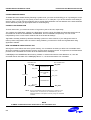
MEMORY FORMATS
ARM7TDMI views memory as a linear collection of bytes numbered upwards from zero. Bytes 0 to 3 hold the first
stored word, bytes 4 to 7 the second and so on. ARM7TDMI can treat words in memory as being stored either in
Big-Endian or Little-Endian format.
2-1
PROGRAMMER’S MODEL
KS32C50100 RISC MICROCONTROLER
BIG-ENDIAN FORMAT
In Big-Endian format, the most significant byte of a word is stored at the lowest numbered byte and the least
significant byte at the highest numbered byte. Byte 0 of the memory system is therefore connected to data lines 31
through 24.
Higher Address
Lower Address
31
24
23
16
15
8
7
0
Word Address
8
9
10
11
8
4
5
6
7
4
0
1
2
3
0
• Most significant byte is at lowest address
• Word is addressed by byte address of most significant byte
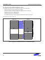
Figure 2-1. Big-Endian Addresses of Bytes within Words
NOTE
The data locations in the external memory are different with Figure 2-1 in the KS32C6200. Please refer to
the chapter 4, System Manager.
LITTLE-ENDIAN FORMAT
In Little-Endian format, the lowest numbered byte in a word is considered the word’s least significant byte, and the
highest numbered byte the most significant. Byte 0 of the memory system is therefore connected to data lines 7
through 0.
Higher Address
Lower Address
31
24
23
16
15
8
7
0
Word Address
11
10
9
8
8
7
6
5
4
4
3
2
1
0
0
• Least significant byte is at lowest address
• Word is addressed by byte address of least significant byte
Figure 2-2. Little-Endian Addresses of Bytes within Words
INSTRUCTION LENGTH
Instructions are either 32 bits long (in ARM state) or 16 bits long (in THUMB state).
Data Types
ARM7TDMI supports byte (8-bit), halfword (16-bit) and word (32-bit) data types. Words must be aligned to four-byte
boundaries and half words to two-byte boundaries.
2-2
KS32C50100 RISC MICROCONTROLLER
PROGRAMMER’S MODEL
OPERATING MODES
ARM7TDMI supports seven modes of operation:
•
User (usr):
The normal ARM program execution state
•
FIQ (fiq):
Designed to support a data transfer or channel process
•
IRQ (irq):
Used for general-purpose interrupt handling
•
Supervisor (svc):
Protected mode for the operating system
•
Abort mode (abt):
Entered after a data or instruction prefetch abort
•
System (sys):
A privileged user mode for the operating system
•
Undefined (und):
Entered when an undefined instruction is executed
Mode changes may be made under software control, or may be brought about by external interrupts or exception
processing. Most application programs will execute in User mode. The non-user modes—known as privileged
modes—are entered in order to service interrupts or exceptions, or to access protected resources.
REGISTERS
ARM7TDMI has a total of 37 registers - 31 general-purpose 32-bit registers and six status registers - but these
cannot all be seen at once. The processor state and operating mode dictate which registers are available to the
programmer.
The ARM State Register Set
In ARM state, 16 general registers and one or two status registers are visible at any one time. In privileged (nonUser) modes, mode-specific banked registers are switched in. Figure 2-3 shows which registers are available in
each mode: the banked registers are marked with a shaded triangle.
The ARM state register set contains 16 directly accessible registers: R0 to R15. All of these except R15 are
general-purpose, and may be used to hold either data or address values. In addition to these, there is a
seventeenth register used to store status information
Register 14
is used as the subroutine link register. This receives a copy of R15 when a Branch and
Link (BL) instruction is executed. At all other times it may be treated as a generalpurpose register. The corresponding banked registers R14_svc, R14_irq, R14_fiq,
R14_abt and R14_und are similarly used to hold the return values of R15 when
interrupts and exceptions arise, or when Branch and Link instructions are executed
within interrupt or exception routines.
Register 15
holds the Program Counter (PC). In ARM state, bits [1:0] of R15 are zero and bits [31:2]
contain the PC. In THUMB state, bit [0] is zero and bits [31:1] contain the PC.
Register 16
is the CPSR (Current Program Status Register). This contains condition code flags and
the current mode bits.
FIQ mode has seven banked registers mapped to R8-14 (R8_fiq-R14_fiq). In ARM state, many FIQ handlers do not
need to save any registers. User, IRQ, Supervisor, Abort and Undefined each have two banked registers mapped
to R13 and R14, allowing each of these modes to have a private stack pointer and link registers.
2-3
PROGRAMMER’S MODEL
KS32C50100 RISC MICROCONTROLER
ARM State General Registers and Program Counter
System & User
FIQ
Supervisor
Abort
IRQ
Undefined
R0
R0
R0
R0
R0
R0
R1
R1
R1
R1
R1
R1
R2
R2
R2
R2
R2
R2
R3
R3
R3
R3
R3
R3
R4
R4
R4
R4
R4
R4
R5
R5
R5
R5
R5
R5
R6
R6
R6
R6
R6
R6
R7
R7
R7
R7
R7
R7
R8
R8_fiq
R8
R8
R8
R8
R9
R9_fiq
R9
R9
R9
R9
R10
R10_fiq
R10
R10
R10
R10
R11
R11_fiq
R11
R11
R11
R11
R12
R12_fiq
R12
R12
R12
R12
R13
R13_fiq
R13_svc
R13_abt
R13_irq
R13_und
R14
R14_fiq
R14_svc
R14_abt
R14_irq
R14_und
R15 (PC)
R15 (PC)
R15 (PC)
R15 (PC)
R15 (PC)
R15 (PC)
ARM State Program Status Registers
CPSR
CPSR
CPSR
CPSR
CPSR
CPSR
SPSR_fiq
SPSR_svc
SPSR_abt
SPSR_irq
SPSR_und
= banked register
Figure 2-3. Register Organization in ARM State
2-4
KS32C50100 RISC MICROCONTROLLER
PROGRAMMER’S MODEL
The THUMB State Register Set
The THUMB state register set is a subset of the ARM state set. The programmer has direct access to eight general
registers, R0-R7, as well as the Program Counter (PC), a stack pointer register (SP), a link register (LR), and the
CPSR. There are banked Stack Pointers, Link Registers and Saved Process Status Registers (SPSRs) for each
privileged mode. This is shown in Figure 2-4.
THUMB State General Registers and Program Counter
System & User
FIQ
Supervisor
Abort
IRQ
Undefined
R0
R0
R0
R0
R0
R0
R1
R1
R1
R1
R1
R1
R2
R2
R2
R2
R2
R2
R3
R3
R3
R3
R3
R3
R4
R4
R4
R4
R4
R4
R5
R5
R5
R5
R5
R5
R6
R6
R6
R6
R6
R6
R7
R7
R7
R7
R7
R7
SP
SP_fiq
SP_svc
SP_abt
SP_irq
SP_und
LR
LR_fiq
LR_svc
LR_abt
LR_irq
LR_und
PC
PC
PC
PC
PC
PC
THUMB State Program Status Registers
CPSR
CPSR
CPSR
CPSR
CPSR
CPSR
SPSR_fiq
SPSR_svc
SPSR_abt
SPSR_irq
SPSR_und
= banked register
Figure 2-4. Register Organization in THUMB State
2-5
PROGRAMMER’S MODEL
KS32C50100 RISC MICROCONTROLER
The relationship between ARM and THUMB state registers
The THUMB state registers relate to the ARM state registers in the following way:
•
THUMB state R0-R7 and ARM state R0-R7 are identical
•
THUMB state CPSR and SPSRs and ARM state CPSR and SPSRs are identical
•
THUMB state SP maps onto ARM state R13
•
THUMB state LR maps onto ARM state R14
•
The THUMB state Program Counter maps onto the ARM state Program Counter (R15)
This relationship is shown in Figure 2-5.
ARM state
R0
R0
R1
R1
R2
R2
R3
R3
R4
R4
R5
R5
R6
R6
R7
R7
Lo-registers
THUMB state
R8
R9
R11
R12
Stack Pointer (SP)
Stack Pointer (R13)
Link Register (LR)
Link Register (R14)
Program Counter (PC )
Hi-registers
R10
Program Counter (R15)
CPSR
CPSR
SPSR
SPSR
Figure 2-5. Mapping of THUMB State Registers onto ARM State Registers
2-6
KS32C50100 RISC MICROCONTROLLER
PROGRAMMER’S MODEL
Accessing Hi-Registers in THUMB State
In THUMB state, registers R8-R15 (the Hi registers) are not part of the standard register set. However, the assembly
language programmer has limited access to them, and can use them for fast temporary storage.
A value may be transferred from a register in the range R0-R7 (a Lo register) to a Hi register, and from a Hi register
to a Lo register, using special variants of the MOV instruction. Hi register values can also be compared against or
added to Lo register values with the CMP and ADD instructions. For more information, refer to Figure 3-34.
THE PROGRAM STATUS REGISTERS
The ARM7TDMI contains a Current Program Status Register (CPSR), plus five Saved Program Status Registers
(SPSRs) for use by exception handlers. These register’s functions are:
•
Hold information about the most recently performed ALU operation
•
Control the enabling and disabling of interrupts
•
Set the processor operating mode
The arrangement of bits is shown in Figure 2-6.
condition code flags
(reserved)
31
30
29
28
27
26
N
Z
C
V
.
.
25 24
.
.
control bits
23
.
.
8
7
6
5
.
I
F
T
4
3
2
M4 M3 M2
Overflow
Carry / Borrow
/ Extend
Zero
Negative / Less Than
1
0
M1 M0
Mode bits
State bit
FIQ disable
IRQ disable
Figure 2-6 . Program Status Register Format
2-7
PROGRAMMER’S MODEL
KS32C50100 RISC MICROCONTROLER
The Condition Code Flags
The N, Z, C and V bits are the condition code flags. These may be changed as a result of arithmetic and logical
operations, and may be tested to determine whether an instruction should be executed.
In ARM state, all instructions may be executed conditionally: see Table 3-2 for details.
In THUMB state, only the Branch instruction is capable of conditional execution: see Figure 3-46 for details.
The Control Bits
The bottom 8 bits of a PSR (incorporating I, F, T and M[4:0]) are known collectively as the control bits. These will
change when an exception arises. If the processor is operating in a privileged mode, they can also be manipulated
by software.
The T bit
This reflects the operating state. When this bit is set, the processor is executing in
THUMB state, otherwise it is executing in ARM state. This is reflected on the TBIT
external signal.
Note that the software must never change the state of the TBIT in the CPSR. If this
happens, the processor will enter an unpredictable state.
Interrupt disable bits
The I and F bits are the interrupt disable bits. When set, these disable the IRQ and FIQ
interrupts respectively.
The mode bits
The M4, M3, M2, M1 and M0 bits (M[4:0]) are the mode bits. These determine the
processor’s operating mode, as shown in Table 2-1. Not all combinations of the mode
bits define a valid processor mode. Only those explicitly described shall be used. The
user should be aware that if any illegal value is programmed into the mode bits, M[4:0],
then the processor will enter an unrecoverable state. If this occurs, reset should be
applied.
2-8
KS32C50100 RISC MICROCONTROLLER
PROGRAMMER’S MODEL
Table 2-1. PSR Mode Bit Values
M[4:0]
Reserved bits
Mode
Visible THUMB state
registers
Visible ARM state
registers
10000
User
R7..R0,
LR, SP
PC, CPSR
R14..R0,
PC, CPSR
10001
FIQ
R7..R0,
LR_fiq, SP_fiq
PC, CPSR, SPSR_fiq
R7..R0,
R14_fiq..R8_fiq,
PC, CPSR, SPSR_fiq
10010
IRQ
R7..R0,
LR_irq, SP_irq
PC, CPSR, SPSR_irq
R12..R0,
R14_irq..R13_irq,
PC, CPSR, SPSR_irq
10011
Supervisor
R12..R0,
R7..R0,
R14_svc..R13_svc,
LR_svc, SP_svc,
PC, CPSR, SPSR_svc PC, CPSR, SPSR_svc
10111
Abort
R7..R0,
R12..R0,
LR_abt, SP_abt,
R14_abt..R13_abt,
PC, CPSR, SPSR_abt PC, CPSR, SPSR_abt
11011
Undefined
R7..R0
LR_und, SP_und,
PC, CPSR,
SPSR_und
R12..R0,
R14_und..R13_und,
PC, CPSR
11111
System
R7..R0,
LR, SP
PC, CPSR
R14..R0,
PC, CPSR
The remaining bits in the PSRs are reserved. When changing a PSR’s flag or control
bits, you must ensure that these unused bits are not altered. Also, your program should
not rely on them containing specific values, since in future processors they may read as
one or zero.
2-9
PROGRAMMER’S MODEL
KS32C50100 RISC MICROCONTROLER
EXCEPTIONS
Exceptions arise whenever the normal flow of a program has to be halted temporarily, for example to service an
interrupt from a peripheral. Before an exception can be handled, the current processor state must be preserved so
that the original program can resume when the handler routine has finished.
It is possible for several exceptions to arise at the same time. If this happens, they are dealt with in a fixed order.
See Exception Priorities on page 2-14.
Action on Entering an Exception
When handling an exception, the ARM7TDMI:
1.
Preserves the address of the next instruction in the appropriate Link Register. If the
exception has been entered from ARM state, then the address of the next instruction is
copied into the Link Register (that is, current PC + 4 or PC + 8 depending on the
exception. See Table 2-2 on for details). If the exception has been entered from THUMB
state, then the value written into the Link Register is the current PC offset by a value
such that the program resumes from the correct place on return from the exception.
This means that the exception handler need not determine which state the exception
was entered from. For example, in the case of SWI, MOVS PC, R14_svc will always
return to the next instruction regardless of whether the SWI was executed in ARM or
THUMB state.
2.
Copies the CPSR into the appropriate SPSR
3.
Forces the CPSR mode bits to a value which depends on the exception
4.
Forces the PC to fetch the next instruction from the relevant exception vector
It may also set the interrupt disable flags to prevent otherwise unmanageable nestings of exceptions.
If the processor is in THUMB state when an exception occurs, it will automatically switch into ARM state when the
PC is loaded with the exception vector address.
Action on Leaving an Exception
On completion, the exception handler:
1.
Moves the Link Register, minus an offset where appropriate, to the PC. (The offset will
vary depending on the type of exception.)
2.
Copies the SPSR back to the CPSR
3.
Clears the interrupt disable flags, if they were set on entry
NOTE
An explicit switch back to THUMB state is never needed, since restoring the CPSR from the SPSR
automatically sets the T bit to the value it held immediately prior to the exception.
2-10
KS32C50100 RISC MICROCONTROLLER
PROGRAMMER’S MODEL
Exception Entry/Exit Summary
Table 2-2 summarises the PC value preserved in the relevant R14 on exception entry, and the recommended
instruction for exiting the exception handler.
Table 2-2. Exception Entry/Exit
Return Instruction
Previous State
Notes
ARM
R14_x
THUMB
R14_x
BL
MOV PC, R14
PC + 4
PC + 2
1
SWI
MOVS PC, R14_svc
PC + 4
PC + 2
1
UDEF
MOVS PC, R14_und
PC + 4
PC + 2
1
FIQ
SUBS PC, R14_fiq, #4
PC + 4
PC + 4
2
IRQ
SUBS PC, R14_irq, #4
PC + 4
PC + 4
2
PABT
SUBS PC, R14_abt, #4
PC + 4
PC + 4
1
DABT
SUBS PC, R14_abt, #8
PC + 8
PC + 8
3
RESET
NA
–
–
4
NOTES
1. Where PC is the address of the BL/SWI/Undefined Instruction fetch which had the prefetch abort.
2. Where PC is the address of the instruction which did not get executed since the FIQ or IRQ took priority.
3. Where PC is the address of the Load or Store instruction which generated the data abort.
4. The value saved in R14_svc upon reset is unpredictable.
FIQ
The FIQ (Fast Interrupt Request) exception is designed to support a data transfer or channel process, and in ARM
state has sufficient private registers to remove the need for register saving (thus minimising the overhead of context
switching).
FIQ is externally generated by taking the nFIQ input LOW. This input can except either synchronous or
asynchronous transitions, depending on the state of the ISYNC input signal. When ISYNC is LOW, nFIQ and nIRQ
are considered asynchronous, and a cycle delay for synchronization is incurred before the interrupt can affect the
processor flow.
Irrespective of whether the exception was entered from ARM or Thumb state, a FIQ handler should leave the
interrupt by executing
SUBS PC,R14_fiq,#4
FIQ may be disabled by setting the CPSR’s F flag (but note that this is not possible from User mode). If the F flag is
clear, ARM7TDMI checks for a LOW level on the output of the FIQ synchroniser at the end of each instruction.
2-11
PROGRAMMER’S MODEL
KS32C50100 RISC MICROCONTROLER
IRQ
The IRQ (Interrupt Request) exception is a normal interrupt caused by a LOW level on the nIRQ input. IRQ has a
lower priority than FIQ and is masked out when a FIQ sequence is entered. It may be disabled at any time by
setting the I bit in the CPSR, though this can only be done from a privileged (non-User) mode.
Irrespective of whether the exception was entered from ARM or Thumb state, an IRQ handler should return from
the interrupt by executing
SUBS PC,R14_irq,#4
Abort
An abort indicates that the current memory access cannot be completed. It can be signalled by the external
ABORT input. ARM7TDMI checks for the abort exception during memory access cycles.
There are two types of abort:
•
Prefetch abort: occurs during an instruction prefetch.
•
Data abort: occurs during a data access.
If a prefetch abort occurs, the prefetched instruction is marked as invalid, but the exception will not be taken until
the instruction reaches the head of the pipeline. If the instruction is not executed - for example because a branch
occurs while it is in the pipeline - the abort does not take place.
If a data abort occurs, the action taken depends on the instruction type:
•
Single data transfer instructions (LDR, STR) write back modified base registers: the Abort handler must be
aware of this.
•
The swap instruction (SWP) is aborted as though it had not been executed.
•
Block data transfer instructions (LDM, STM) complete. If write-back is set, the base is updated. If the instruction
would have overwritten the base with data (ie it has the base in the transfer list), the overwriting is prevented.
All register overwriting is prevented after an abort is indicated, which means in particular that R15 (always the
last register to be transferred) is preserved in an aborted LDM instruction.
The abort mechanism allows the implementation of a demand paged virtual memory system. In such a system the
processor is allowed to generate arbitrary addresses. When the data at an address is unavailable, the Memory
Management Unit (MMU) signals an abort. The abort handler must then work out the cause of the abort, make the
requested data available, and retry the aborted instruction. The application program needs no knowledge of the
amount of memory available to it, nor is its state in any way affected by the abort.
After fixing the reason for the abort, the handler should execute the following irrespective of the state (ARM or
Thumb):
SUBS PC,R14_abt,#4
SUBS PC,R14_abt,#8
; for a prefetch abort, or
; for a data abort
This restores both the PC and the CPSR, and retries the aborted instruction.
2-12
KS32C50100 RISC MICROCONTROLLER
PROGRAMMER’S MODEL
Software Interrupt
The software interrupt instruction (SWI) is used for entering Supervisor mode, usually to request a particular
supervisor function. A SWI handler should return by executing the following irrespective of the state (ARM or
Thumb):
MOV PC,R14_svc
This restores the PC and CPSR, and returns to the instruction following the SWI.
NOTE
nFIQ, nIRQ, ISYNC, LOCK, BIGEND, and ABORT pins exist only in the internal ARM7TDMI CPU core.
Undefined Instruction
When ARM7TDMI comes across an instruction which it cannot handle, it takes the undefined instruction trap. This
mechanism may be used to extend either the THUMB or ARM instruction set by software emulation.
After emulating the failed instruction, the trap handler should execute the following irrespective of the state (ARM or
Thumb):
MOVS PC,R14_und
This restores the CPSR and returns to the instruction following the undefined instruction.
Exception Vectors
The following table shows the exception vector addresses.
Table 2-3. Exception Vectors
Address
Exception
Mode on entry
0x00000000
Reset
Supervisor
0x00000004
Undefined instruction
Undefined
0x00000008
Software interrupt
Supervisor
0x0000000C
Abort (prefetch)
Abort
0x00000010
Abort (data)
Abort
0x00000014
Reserved
Reserved
0x00000018
IRQ
IRQ
0x0000001C
FIQ
FIQ
2-13
PROGRAMMER’S MODEL
KS32C50100 RISC MICROCONTROLER
Exception Priorities
When multiple exceptions arise at the same time, a fixed priority system determines the order in which they are
handled:
Highest priority:
1. Reset
2. Data abort
3. FIQ
4. IRQ
5. Prefetch abort
Lowest priority:
6. Undefined Instruction, Software interrupt.
Not All Exceptions Can Occur at Once:
Undefined Instruction and Software Interrupt are mutually exclusive, since they each correspond to particular (nonoverlapping) decodings of the current instruction.
If a data abort occurs at the same time as a FIQ, and FIQs are enabled (ie the CPSR’s F flag is clear), ARM7TDMI
enters the data abort handler and then immediately proceeds to the FIQ vector. A normal return from FIQ will cause
the data abort handler to resume execution. Placing data abort at a higher priority than FIQ is necessary to ensure
that the transfer error does not escape detection. The time for this exception entry should be added to worst-case
FIQ latency calculations.
INTERRUPT LATENCIES
The worst case latency for FIQ, assuming that it is enabled, consists of the longest time the request can take to pass
through the synchroniser (Tsyncmax if asynchronous), plus the time for the longest instruction to complete (Tldm,
the longest instruction is an LDM which loads all the registers including the PC), plus the time for the data abort entry
(Texc), plus the time for FIQ entry (Tfiq). At the end of this time ARM7TDMI will be executing the instruction at 0x1C.
Tsyncmax is 3 processor cycles, Tldm is 20 cycles, Texc is 3 cycles, and Tfiq is 2 cycles. The total time is therefore
28 processor cycles. This is just over 1.4 microseconds in a system which uses a continuous 20 MHz processor
clock. The maximum IRQ latency calculation is similar, but must allow for the fact that FIQ has higher priority and
could delay entry into the IRQ handling routine for an arbitrary length of time. The minimum latency for FIQ or IRQ
consists of the shortest time the request can take through the synchroniser (Tsyncmin) plus Tfiq. This is 4
processor cycles.
RESET
When the nRESET signal goes LOW, ARM7TDMI abandons the executing instruction and then continues to fetch
instructions from incrementing word addresses.
When nRESET goes HIGH again, ARM7TDMI:
1. Overwrites R14_svc and SPSR_svc by copying the current values of the PC and CPSR into them. The value of
the saved PC and SPSR is not defined.
2. Forces M[4:0] to 10011 (Supervisor mode), sets the I and F bits in the CPSR, and clears the CPSR’s T bit.
3. Forces the PC to fetch the next instruction from address 0x00.
4. Execution resumes in ARM state.
2-14
KS32C50100 RISC MICROCONTROLLER
3
ARM INSTRUCTION SET
Instruction set
INSTRUCTION SET SUMMAY
This chapter describes the ARM instruction set and the THUMB instruction set in the ARM7TDMI core.
FORMAT SUMMARY
The ARM instruction set formats are shown below.
31 30 29 28 27 26 25 24 23 22 21 20 19 18 17 16 15 14 13 12 11 10 9 8 7 6 5 4 3 2 1 0
Cond
0
0
I
Opcode
S
Rn
Rd
Cond
0
0
0
0
0
Cond
0
0
0
0
1 U A S
Cond
0
0
0
1
0 B 0
0
Cond
0
0
0
1
0
0 A S
Rd
Rn
Rs
1
0
0
1
Rm
Multiply
RdHi
RdLo
Rn
1
0
0
1
Rm
Multiply Long
Rn
Rd
0
Cond
0
0
0 P U 0 W L
Rn
Rd
Cond
0
0
0 P U 1 W L
Rn
Rd
Cond
0
1
I
Rn
Rd
Cond
0
1
1
Cond
1
0
0 P U S W L
Cond
1
0
1 L
Cond
1
1
0 P U N W L
Cond
1
1
1
0
Cond
1
1
1
0
Cond
1
1
1
1
0
1
P U B W L
1
1
1
1
1
1
1
Operand 2
1
Data Processing /
PSR Transfer
0
0
0
0
1
0
0
1
Rm
Single Data Swap
1
1
1
1
0
0
0
1
Rn
Branch and Exchange
0
0
0
0
1 S H 1
Rm
Halfword Data Tranfer:
register offset
1 S H 1
Offset
Halfword Data Transfer:
immediate offset
Offset
Offset
Single Data Transfer
1
Rn
Undefined
Register List
Block Data Transfer
Offset
CP Opc
CP Opc
L
Branch
Rn
CRd
CP#
Offset
Coprocessor Data
Transfer
CRn
CRd
CP#
CP
0
CRm
Coprocessor Data
Operation
CRn
Rd
CP#
CP
1
CRm
Coprocessor Register
Transfer
Ignored by processor
Software Interrupt
31 30 29 28 27 26 25 24 23 22 21 20 19 18 17 16 15 14 13 12 11 10 9 8 7 6 5 4 3 2 1 0
Figure 3-1. ARM Instruction Set Format
NOTE
Some instruction codes are not defined but do not cause the Undefined instruction trap to be taken, for
instance a Multiply instruction with bit 6 changed to a 1. These instructions should not be used, as their
action may change in future ARM implementations.
3-1
ARM INSTRUCTION SET
KS32C50100 RISC MICROCONTROLER
INSTRUCTION SUMMARY
Table 3-1. The ARM Instruction Set
Mnemonic
3-2
Instruction
Action
ADC
Add with carry
Rd: = Rn + Op2 + Carry
ADD
Add
Rd: = Rn + Op2
AND
AND
Rd: = Rn AND Op2
B
Branch
R15: = address
BIC
Bit Clear
Rd: = Rn AND NOT Op2
BL
Branch with Link
R14: = R15, R15: = address
BX
Branch and Exchange
R15: = Rn,
T bit: = Rn[0]
CDP
Coprocesor Data
Processing
(Coprocessor-specific)
CMN
Compare Negative
CPSR flags: = Rn + Op2
CMP
Compare
CPSR flags: = Rn – Op2
EOR
Exclusive OR
Rd: = (Rn AND NOT Op2)
OR (op2 AND NOT Rn)
LDC
Load coprocessor from
memory
Coprocessor load
LDM
Load multiple registers
Stack manipulation (Pop)
LDR
Load register from memory Rd: = (address)
MCR
Move CPU register to
coprocessor register
cRn: = rRn {<op>cRm}
MLA
Multiply Accumulate
Rd: = (Rm * Rs) + Rn
MOV
Move register or constant
Rd: = Op2
MRC
Move from coprocessor
register to CPU register
Rn: = cRn {<op>cRm}
MRS
Move PSR status/flags to
register
Rn: = PSR
MSR
Move register to PSR
status/flags
PSR: = Rm
MUL
Multiply
Rd: = Rm * Rs
MVN
Move negative register
Rd: = 0xFFFFFFFF EOR
Op2
ORR
OR
Rd: = Rn OR Op2
RSB
Reverse Subtract
Rd: = Op2 – Rn
RSC
Reverse Subtract with
Carry
Rd: = Op2 – Rn – 1 + Carry
KS32C50100 RISC MICROCONTROLLER
ARM INSTRUCTION SET
Table 3-1. The ARM Instruction Set (Continued)
Mnemonic
Instruction
Action
SBC
Subtract with Carry
Rd: = Rn – Op2 - 1 + Carry
STC
Store coprocessor register
to memory
address: = CRn
STM
Store Multiple
Stack manipulation (Push)
STR
Store register to memory
<address>: = Rd
SUB
Subtract
Rd: = Rn – Op2
SWI
Software Interrupt
OS call
SWP
Swap register with
memory
Rd: = [Rn], [Rn] := Rm
TEQ
Test bitwise equality
CPSR flags: = Rn EOR Op2
TST
Test bits
CPSR flags: = Rn AND Op2
3-3
ARM INSTRUCTION SET
KS32C50100 RISC MICROCONTROLER
THE CONDITION FIELD
In ARM state, all instructions are conditionally executed according to the state of the CPSR condition codes and the
instruction’s condition field. This field (bits 31:28) determines the circumstances under which an instruction is to be
executed. If the state of the C, N, Z and V flags fulfils the conditions encoded by the field, the instruction is
executed, otherwise it is ignored.
There are sixteen possible conditions, each represented by a two-character suffix that can be appended to the
instruction’s mnemonic. For example, a Branch (B in assembly language) becomes BEQ for "Branch if Equal",
which means the Branch will only be taken if the Z flag is set.
In practice, fifteen different conditions may be used: these are listed in Table 3-2. The sixteenth (1111) is reserved,
and must not be used.
In the absence of a suffix, the condition field of most instructions is set to "Always" (sufix AL). This means the
instruction will always be executed regardless of the CPSR condition codes.
Table 3-2. Condition Code Summary
Code
3-4
Suffix
Flags
Meaning
0000
EQ
Z set
equal
0001
NE
Z clear
not equal
0010
CS
C set
unsigned higher or same
0011
CC
C clear
unsigned lower
0100
MI
N set
negative
0101
PL
N clear
positive or zero
0110
VS
V set
overflow
0111
VC
V clear
no overflow
1000
HI
C set and Z clear
unsigned higher
1001
LS
C clear or Z set
unsigned lower or same
1010
GE
N equals V
greater or equal
1011
LT
N not equal to V
less than
1100
GT
Z clear AND (N equals V)
greater than
1101
LE
Z set OR (N not equal to V)
less than or equal
1110
AL
(ignored)
always
KS32C50100 RISC MICROCONTROLLER
ARM INSTRUCTION SET
BRANCH AND EXCHANGE (BX)
This instruction is only executed if the condition is true. The various conditions are defined in Table 3-2.
This instruction performs a branch by copying the contents of a general register, Rn, into the program counter, PC.
The branch causes a pipeline flush and refill from the address specified by Rn. This instruction also permits the
instruction set to be exchanged. When the instruction is executed, the value of Rn[0] determines whether the
instruction stream will be decoded as ARM or THUMB instructions.
31
28 27
Cond
24 23
20 19
16 15
12 11
8
7
0 0 0 1 0 0 1 0 1 1 1 1 1 1 1 1 1 1 1 1 0 0 0
4
1
3
0
Rn
[3:0] Operand register
If bit 0 of Rn = 1, subsequent instructions decoded as THUMB instructions
If bit 0 of Rn = 0, subsequent instructions decoded as ARM instructions
[31:28] Condition Field
Figure 3-2. Branch and Exchange Instructions
INSTRUCTION CYCLE TIMES
The BX instruction takes 2S + 1N cycles to execute, where S and N are defined as sequential (S-cycle) and nonsequencial (N-cycle), respectively.
ASSEMBLER SYNTAX
BX - branch and exchange.
BX {cond} Rn
{cond}
Two character condition mnemonic. See Table 3-2.
Rn
is an expression evaluating to a valid register number.
USING R15 AS AN OPERAND
If R15 is used as an operand, the behaviour is undefined.
3-5
ARM INSTRUCTION SET
KS32C50100 RISC MICROCONTROLER
Examples
ADR
R0, Into_THUMB + 1
BX
R0
CODE16
Into_THUMB
.
.
.
ADR R5, Back_to_ARM
BX R5
.
.
.
ALIGN
CODE32
Back_to_ARM
3-6
;
;
;
;
;
;
;
Generate branch target address
and set bit 0 high - hence
arrive in THUMB state.
Branch and change to THUMB
state.
Assemble subsequent code as
THUMB instructions
: Generate branch target to word aligned address
; - hence bit 0 is low and so change back to ARM state.
; Branch and change back to ARM state.
; Word align
; Assemble subsequent code as ARM instructions
KS32C50100 RISC MICROCONTROLLER
ARM INSTRUCTION SET
BRANCH AND BRANCH WITH LINK (B, BL)
The instruction is only executed if the condition is true. The various conditions are defined Table 3-2. The instruction
encoding is shown in Figure 3-3, below.
31
28
Cond
27
25 24
101
23
0
L
offset
[24] Link bit
0 = Branch
1 = Branch with link
[31:28] Condition field
Figure 3-3. Branch Instructions
Branch instructions contain a signed 2's complement 24 bit offset. This is shifted left two bits, sign extended to 32
bits, and added to the PC. The instruction can therefore specify a branch of +/- 32Mbytes. The branch offset must
take account of the prefetch operation, which causes the PC to be 2 words (8 bytes) ahead of the current
instruction.
Branches beyond +/- 32Mbytes must use an offset or absolute destination which has been previously loaded into a
register. In this case the PC should be manually saved in R14 if a Branch with Link type operation is required.
THE LINK BIT
Branch with Link (BL) writes the old PC into the link register (R14) of the current bank. The PC value written into
R14 is adjusted to allow for the prefetch, and contains the address of the instruction following the branch and link
instruction. Note that the CPSR is not saved with the PC and R14[1:0] are always cleared.
To return from a routine called by Branch with Link use MOV PC,R14 if the link register is still valid or LDM
Rn!,{..PC} if the link register has been saved onto a stack pointed to by Rn.
INSTRUCTION CYCLE TIMES
Branch and Branch with Link instructions take 2S + 1N incremental cycles, where S and N are defined as squential
(S-cycle) and internal (I-cycle).
3-7
ARM INSTRUCTION SET
KS32C50100 RISC MICROCONTROLER
ASSEMBLER SYNTAX
Items in {} are optional. Items in <> must be present.
B{L}{cond} <expression>
{L}
Used to request the Branch with Link form of the instruction. If absent, R14 will not be
affected by the instruction.
{cond}
A two-character mnemonic as shown in Table 3-2. If absent then AL (ALways) will be
used.
<expression>
The destination. The assembler calculates the offset.
EXAMPLES
here
3-8
BAL
B
CMP
here
there
R1,#0
BEQ
fred
BL
ADDS
sub+ROM
R1,#1
BLCC
sub
;
;
;
;
;
Assembles to 0xEAFFFFFE (note effect of PC offset).
Always condition used as default.
Compare R1 with zero and branch to fred
if R1 was zero, otherwise continue.
Continue to next instruction.
;
;
;
;
;
Call subroutine at computed address.
Add 1 to register 1, setting CPSR flags
on the result then call subroutine if
the C flag is clear, which will be the
case unless R1 held 0xFFFFFFFF.
KS32C50100 RISC MICROCONTROLLER
ARM INSTRUCTION SET
DATA PROCESSING
The data processing instruction is only executed if the condition is true. The conditions are defined in Table 3-2. The
instruction encoding is shown in Figure 3-4.
31
28
Cond
27
26
00
25
I
24
21
OpCode
20
19
S
16
15
12
Rn
11
10
Rd
0
Operand 2
[15:12] Destination register
0 = Branch
1 = Branch with Link
[19:16] 1st operand register
0 = Branch
1 = Branch with Link
[20] Set condition codes
0 = Do not after condition codes
1 = Set condition codes
[24:21] Operation code
0000 = AND - Rd: = Op1 AND Op2
0001 = EOR - Rd: = Op1 EOR Op2
0010 = SUB - Rd: = Op1 - Op2
0011 = RSB - Rd: = Op2 - Op1
0100 = ADD - Rd: = Op1 + Op2
0101 = ADC - Rd: = Op1 + Op2 + C
0110 = SBC - Rd: = Op1 - Op2 + C - 1
0111 = RSC - Rd: = Op2 - Op1 + C - 1
1000 = TST - set condition codes on Op 1 AND Op2
1001 = TEO - set condition codes on Op1 EOR Op2
1010 = CMP - set condition codes on Op1 - Op2
1011 = SMN - set condition codes on Op1 + Op2
1100 = ORR - Rd: = Op1 OR Op2
1101 = MOV - Rd: = Op2
1110 = BIC - Rd: = Op1 AND NOT Op2
1111 = MVN - Rd: = NOT Op2
[25] Immediate operand
0 = Operand 2 is a register
1 = Operand 2 is an Immediate Value
[11:0] Operand 2 type selection
11
4
3
0
Shift
Rm
[3:0] 2nd Operand Register
11
8
[11:4] Shift Applied to Rm
7
Rotate
0
Imm
[7:0] Unsigned 8 bit immediate value
[11:8] Shift applied to lmm
[31:28] Condition field
Figure 3-4. Data Processing Instructions
3-9
ARM INSTRUCTION SET
KS32C50100 RISC MICROCONTROLER
The instruction produces a result by performing a specified arithmetic or logical operation on one or two operands.
The first operand is always a register (Rn).
The second operand may be a shifted register (Rm) or a rotated 8 bit immediate value (Imm) according to the value
of the I bit in the instruction. The condition codes in the CPSR may be preserved or updated as a result of this
instruction, according to the value of the S bit in the instruction.
Certain operations (TST, TEQ, CMP, CMN) do not write the result to Rd. They are used only to perform tests and to
set the condition codes on the result and always have the S bit set. The instructions and their effects are listed in
Table 3-3.
3-10
KS32C50100 RISC MICROCONTROLLER
ARM INSTRUCTION SET
CPSR FLAGS
The data processing operations may be classified as logical or arithmetic. The logical operations (AND, EOR, TST,
TEQ, ORR, MOV, BIC, MVN) perform the logical action on all corresponding bits of the operand or operands to
produce the result. If the S bit is set (and Rd is not R15, see below) the V flag in the CPSR will be unaffected, the C
flag will be set to the carry out from the barrel shifter (or preserved when the shift operation is LSL #0), the Z flag will
be set if and only if the result is all zeros, and the N flag will be set to the logical value of bit 31 of the result.
Table 3-3. ARM Data Processing Instructions
Assembler
Mnemonic
Op-Code
Action
AND
0000
Operand1 AND operand2
EOR
0001
Operand1 EOR operand2
SUB
0010
Operand1 – operand2
RSB
0011
Operand2 operand1
ADD
0100
Operand1 + operand2
ADC
0101
Operand1 + operand2 + carry
SBC
0110
Operand1 – operand2 + carry – 1
RSC
0111
Operand2 – operand1 + carry – 1
TST
1000
As AND, but result is not written
TEQ
1001
As EOR, but result is not written
CMP
1010
As SUB, but result is not written
CMN
1011
As ADD, but result is not written
ORR
1100
Operand1 OR operand2
MOV
1101
Operand2 (operand1 is ignored)
BIC
1110
Operand1 AND NOT operand2 (Bit clear)
MVN
1111
NOT operand2 (operand1 is ignored)
The arithmetic operations (SUB, RSB, ADD, ADC, SBC, RSC, CMP, CMN) treat each operand as a 32 bit integer
(either unsigned or 2's complement signed, the two are equivalent). If the S bit is set (and Rd is not R15) the V flag
in the CPSR will be set if an overflow occurs into bit 31 of the result; this may be ignored if the operands were
considered unsigned, but warns of a possible error if the operands were 2's complement signed. The C flag will be
set to the carry out of bit 31 of the ALU, the Z flag will be set if and only if the result was zero, and the N flag will be
set to the value of bit 31 of the result (indicating a negative result if the operands are considered to be 2's
complement signed).
3-11
ARM INSTRUCTION SET
KS32C50100 RISC MICROCONTROLER
SHIFTS
When the second operand is specified to be a shifted register, the operation of the barrel shifter is controlled by the
Shift field in the instruction. This field indicates the type of shift to be performed (logical left or right, arithmetic right
or rotate right). The amount by which the register should be shifted may be contained in an immediate field in the
instruction, or in the bottom byte of another register (other than R15). The encoding for the different shift types is
shown in Figure 3-5.
11
7
6
5
4
11
0
RS
[6:5] Shift type
00 = logical left
10 = arithmetic right
8
7
6
5
0
4
1
[6:5] Shift type
01 = logical right
11 = rotate right
00 = logical left
10 = arithmetic right
[11:7] Shift amount
[11:8] Shift register
5 bit unsigned integer
Shift amount specified in
bottom-byte of Rs
01 = logical right
11 = rotate right
Figure 3-5. ARM Shift Operations
Instruction specified shift amount
When the shift amount is specified in the instruction, it is contained in a 5 bit field which may take any value from 0
to 31. A logical shift left (LSL) takes the contents of Rm and moves each bit by the specified amount to a more
significant position. The least significant bits of the result are filled with zeros, and the high bits of Rm which do not
map into the result are discarded, except that the least significant discarded bit becomes the shifter carry output
which may be latched into the C bit of the CPSR when the ALU operation is in the logical class (see above). For
example, the effect of LSL #5 is shown in Figure 3-6.
31
27 26
0
Contents of Rm
carry out
Value of operand 2
0 0 0 0 0
Figure 3-6. Logical Shift Left
NOTE
LSL #0 is a special case, where the shifter carry out is the old value of the CPSR C flag. The contents of
Rm are used directly as the second operand. A logical shift right (LSR) is similar, but the contents of Rm
are moved to less significant positions in the result. LSR #5 has the effect shown in Figure 3-7.
3-12
KS32C50100 RISC MICROCONTROLLER
ARM INSTRUCTION SET
.
31
5
4
0
Contents of Rm
carry out
0
0 0 0
0
Value of operand 2
Figure 3-7. Logical Shift Right
The form of the shift field which might be expected to correspond to LSR #0 is used to encode LSR #32, which has
a zero result with bit 31 of Rm as the carry output. Logical shift right zero is redundant as it is the same as logical
shift left zero, so the assembler will convert LSR #0 (and ASR #0 and ROR #0) into LSL #0, and allow LSR #32 to
be specified.
An arithmetic shift right (ASR) is similar to logical shift right, except that the high bits are filled with bit 31 of Rm
instead of zeros. This preserves the sign in 2's complement notation. For example, ASR #5 is shown in Figure 3-8.
5
31 30
4
0
Contents of Rm
carry out
Value of operand 2
Figure 3-8. Arithmetic Shift Right
The form of the shift field which might be expected to give ASR #0 is used to encode ASR #32. Bit 31 of Rm is
again used as the carry output, and each bit of operand 2 is also equal to bit 31 of Rm. The result is therefore all
ones or all zeros, according to the value of bit 31 of Rm.
3-13
ARM INSTRUCTION SET
KS32C50100 RISC MICROCONTROLER
Rotate right (ROR) operations reuse the bits which “overshoot” in a logical shift right operation by reintroducing
them at the high end of the result, in place of the zeros used to fill the high end in logical right operations. For
example, ROR #5 is shown in Figure 3-9. The form of the shift field which might be expected to give ROR #0 is
31
5
0
4
Contents of Rm
carry out
Value of operand 2
Figure 3-9. Rotate Right
used to encode a special function of the barrel shifter, rotate right extended (RRX). This is a rotate right by one bit
position of the 33 bit quantity formed by appending the CPSR C flag to the most significant end of the contents of
Rm as shown in Figure 3-10.
31
1
0
Contents of Rm
carry out
C
in
Value of operand 2
Figure 3-10. Rotate Right Extended
3-14
KS32C50100 RISC MICROCONTROLLER
ARM INSTRUCTION SET
Register specified shift amount
Only the least significant byte of the contents of Rs is used to determine the shift amount. Rs can be any general
register other than R15.
If this byte is zero, the unchanged contents of Rm will be used as the second operand, and the old value of the
CPSR C flag will be passed on as the shifter carry output.
If the byte has a value between 1 and 31, the shifted result will exactly match that of an instruction specified shift
with the same value and shift operation.
If the value in the byte is 32 or more, the result will be a logical extension of the shift described above:
1
LSL by 32 has result zero, carry out equal to bit 0 of Rm.
2
LSL by more than 32 has result zero, carry out zero.
3
LSR by 32 has result zero, carry out equal to bit 31 of Rm.
4
LSR by more than 32 has result zero, carry out zero.
5
ASR by 32 or more has result filled with and carry out equal to bit 31 of Rm.
6
ROR by 32 has result equal to Rm, carry out equal to bit 31 of Rm.
7
ROR by n where n is greater than 32 will give the same result and carry out as ROR by n-32; therefore
repeatedly subtract 32 from n until the amount is in the range 1 to 32 and see above.
NOTE
The zero in bit 7 of an instruction with a register controlled shift is compulsory; a one in this bit will cause
the instruction to be a multiply or undefined instruction.
3-15
ARM INSTRUCTION SET
KS32C50100 RISC MICROCONTROLER
IMMEDIATE OPERAND ROTATES
The immediate operand rotate field is a 4 bit unsigned integer which specifies a shift operation on the 8 bit
immediate value. This value is zero extended to 32 bits, and then subject to a rotate right by twice the value in the
rotate field. This enables many common constants to be generated, for example all powers of 2.
WRITING TO R15
When Rd is a register other than R15, the condition code flags in the CPSR may be updated from the ALU flags as
described above.
When Rd is R15 and the S flag in the instruction is not set the result of the operation is placed in R15 and the CPSR
is unaffected.
When Rd is R15 and the S flag is set the result of the operation is placed in R15 and the SPSR corresponding to
the current mode is moved to the CPSR. This allows state changes which atomically restore both PC and CPSR.
This form of instruction should not be used in User mode.
USING R15 AS AN OPERAND
If R15 (the PC) is used as an operand in a data processing instruction the register is used directly.
The PC value will be the address of the instruction, plus 8 or 12 bytes due to instruction prefetching. If the shift
amount is specified in the instruction, the PC will be 8 bytes ahead. If a register is used to specify the shift amount
the PC will be 12 bytes ahead.
TEQ, TST, CMP AND CMN OPCODES
NOTE
TEQ, TST, CMP and CMN do not write the result of their operation but do set flags in the CPSR. An
assembler should always set the S flag for these instructions even if this is not specified in the mnemonic.
The TEQP form of the TEQ instruction used in earlier ARM processors must not be used: the PSR transfer
operations should be used instead.
The action of TEQP in the ARM7TDMI is to move SPSR_<mode> to the CPSR if the processor is in a
privileged mode and to do nothing if in User mode.
INSTRUCTION CYCLE TIMES
Data Processing instructions vary in the number of incremental cycles taken as follows:
Table 3-4. Incremental Cycle Times
Processing Type
Cycles
Normal Data Processing
1S
Data Processing with register specified shift
1S + 1I
Data Processing with PC written
2S + 1N
Data Processing with register specified shift and PC
written
2S + 1N + 1I
NOTE: S, N and I are as defined sequential (S-cycle), non-sequencial (N-cycle), and internal (I-cycle) respectively.
3-16
KS32C50100 RISC MICROCONTROLLER
ARM INSTRUCTION SET
ASSEMBLER SYNTAX
•
MOV,MVN (single operand instructions).
<opcode>{cond}{S} Rd,<Op2>
•
CMP,CMN,TEQ,TST (instructions which do not produce a result).
<opcode>{cond} Rn,<Op2>
•
AND,EOR,SUB,RSB,ADD,ADC,SBC,RSC,ORR,BIC
<opcode>{cond}{S} Rd,Rn,<Op2>
where:
<Op2>
Rm{,<shift>} or,<#expression>
{cond}
A two-character condition mnemonic. See Table 3-2.
{S}
Set condition codes if S present (implied for CMP, CMN, TEQ, TST).
Rd, Rn and Rm
Expressions evaluating to a register number.
<#expression>
If this is used, the assembler will attempt to generate a shifted immediate 8-bit field to
match the expression. If this is impossible, it will give an error.
<shift>
<Shiftname> <register> or <shiftname> #expression, or RRX (rotate right one bit with
extend).
<shiftname>s
ASL, LSL, LSR, ASR, ROR. (ASL is a synonym for LSL, they assemble to the same
code.)
EXAMPLES
ADDEQ
TEQS
R2,R4,R5
R4,#3
SUB
R4,R5,R7,LSR R2
MOV
MOVS
PC,R14
PC,R14
;
;
;
;
;
;
;
;
;
;
If the Z flag is set make R2:=R4+R5
Test R4 for equality with 3.
(The S is in fact redundant as the
assembler inserts it automatically.)
Logical right shift R7 by the number in
the bottom byte of R2, subtract result
from R5, and put the answer into R4.
Return from subroutine.
Return from exception and restore CPSR
from SPSR_mode.
3-17
ARM INSTRUCTION SET
KS32C50100 RISC MICROCONTROLER
PSR TRANSFER (MRS, MSR)
The instruction is only executed if the condition is true. The various conditions are defined in Table 3-2.
The MRS and MSR instructions are formed from a subset of the Data Processing operations and are implemented
using the TEQ, TST, CMN and CMP instructions without the S flag set. The encoding is shown in Figure 3-11.
These instructions allow access to the CPSR and SPSR registers. The MRS instruction allows the contents of the
CPSR or SPSR_<mode> to be moved to a general register. The MSR instruction allows the contents of a general
register to be moved to the CPSR or SPSR_<mode> register.
The MSR instruction also allows an immediate value or register contents to be transferred to the condition code
flags (N,Z,C and V) of CPSR or SPSR_<mode> without affecting the control bits. In this case, the top four bits of
the specified register contents or 32 bit immediate value are written to the top four bits of the relevant PSR.
OPERAND RESTRICTIONS
•
In user mode, the control bits of the CPSR are protected from change, so only the condition code flags of the
CPSR can be changed. In other (privileged) modes the entire CPSR can be changed.
•
Note that the software must never change the state of the T bit in the CPSR. If this happens, the processor will
enter an unpredictable state.
•
The SPSR register which is accessed depends on the mode at the time of execution. For example, only
SPSR_fiq is accessible when the processor is in FIQ mode.
•
You must not specify R15 as the source or destination register.
•
Also, do not attempt to access an SPSR in User mode, since no such register exists.
3-18
KS32C50100 RISC MICROCONTROLLER
ARM INSTRUCTION SET
MRS (transfer PSR contents to a register)
31
28
27
23
Cond
22
21
16
Ps
00010
15
12
11
0
Rd
001111
000000000000
[15:12] Destination register
[22] Source PSR
0 = CPSR
1 = SPSR_<current mode>
[31:28] Condition field
MRS (transfer register contents to PSR)
31
28
27
23
Cond
22
21
12
Pd
00010
11
1010011111
4
3
00000000
0
Rm
[3:0] Source register
[22] Destination PSR
0 = CPSR
1 = SPSR_<current mode>
[31:28] Condition field
MRS (transfer register contents or immdiate value to PSR flag bits only)
31
28
Cond
27
26
00
25
I
24
23
10
22
21
12
Pd
11
0
1010001111
Source operand
[22] Destination PSR
0 = CPSR
1 = SPSR_<current mode>
[25] Immediate Operand
0 = Source operand is a register
1 = SPSR_<current mode>
[11:0] Source operand
11
4
3
00000000
0
Rm
[3:0] Source register
[11:4] Source operand is an immediate value
11
8
7
Rotate
0
Imm
[7:0] Unsigned 8 bit immediate value
[11:8] Shift applied to lmm
[31:28] Condition field
Figure 3-11. PSR Transfer
3-19
ARM INSTRUCTION SET
KS32C50100 RISC MICROCONTROLER
RESERVED BITS
Only twelve bits of the PSR are defined in ARM7TDMI (N,Z,C,V,I,F, T & M[4:0]); the remaining bits are reserved for
use in future versions of the processor. Refer to Figure 2-6 for a full description of the PSR bits.
To ensure the maximum compatibility between ARM7TDMI programs and future processors, the following rules
should be observed:
•
The reserved bits should be preserved when changing the value in a PSR.
•
Programs should not rely on specific values from the reserved bits when checking the PSR status, since they
may read as one or zero in future processors.
A read-modify-write strategy should therefore be used when altering the control bits of any PSR register; this
involves transferring the appropriate PSR register to a general register using the MRS instruction, changing only
the relevant bits and then transferring the modified value back to the PSR register using the MSR instruction.
EXAMPLES
The following sequence performs a mode change:
MRS
BIC
ORR
MSR
R0,CPSR
R0,R0,#0x1F
R0,R0,#new_mode
CPSR,R0
;
;
;
;
Take a copy of the CPSR.
Clear the mode bits.
Select new mode
Write back the modified CPSR.
When the aim is simply to change the condition code flags in a PSR, a value can be written directly to the flag bits
without disturbing the control bits. The following instruction sets the N,Z,C and V flags:
MSR
CPSR_flg,#0xF0000000
; Set all the flags egardless of their previous state
; (does not affect any control bits).
No attempt should be made to write an 8 bit immediate value into the whole PSR since such an operation cannot
preserve the reserved bits.
INSTRUCTION CYCLE TIMES
PSR transfers take 1S incremental cycles, where S is defined as Sequential (S-cycle).
3-20
KS32C50100 RISC MICROCONTROLLER
ARM INSTRUCTION SET
ASSEMBLER SYNTAX
•
MRS - transfer PSR contents to a register
MRS{cond} Rd,<psr>
•
MSR - transfer register contents to PSR
MSR{cond} <psr>,Rm
•
MSR - transfer register contents to PSR flag bits only
MSR{cond} <psrf>,Rm
The most significant four bits of the register contents are written to the N,Z,C & V flags respectively.
•
MSR - transfer immediate value to PSR flag bits only
MSR{cond} <psrf>,<#expression>
The expression should symbolise a 32 bit value of which the most significant four bits are written to the N,Z,C and
V flags respectively.
Key:
{cond}
Two-character condition mnemonic. See Table 3-2..
Rd and Rm
Expressions evaluating to a register number other than R15
<psr>
CPSR, CPSR_all, SPSR or SPSR_all. (CPSR and CPSR_all are synonyms as are
SPSR and SPSR_all)
<psrf>
CPSR_flg or SPSR_flg
<#expression>
Where this is used, the assembler will attempt to generate a shifted immediate 8-bit
field to match the expression. If this is impossible, it will give an error.
EXAMPLES
In User mode the instructions behave as follows:
MSR
MSR
MSR
MRS
CPSR_all,Rm
CPSR_flg,Rm
CPSR_flg,#0xA0000000
Rd,CPSR
;
;
;
;
CPSR[31:28] <- Rm[31:28]
CPSR[31:28] <- Rm[31:28]
CPSR[31:28] <- 0xA (set N,C; clear Z,V)
Rd[31:0] <- CPSR[31:0]
In privileged modes the instructions behave as follows:
MSR
MSR
MSR
MSR
MSR
MSR
MRS
CPSR_all,Rm
CPSR_flg,Rm
CPSR_flg,#0x50000000
SPSR_all,Rm
SPSR_flg,Rm
SPSR_flg,#0xC0000000
Rd,SPSR
;
;
;
;
;
;
;
CPSR[31:0] <- Rm[31:0]
CPSR[31:28] <- Rm[31:28]
CPSR[31:28] <- 0x5 (set Z,V; clear N,C)
SPSR_<mode>[31:0]<- Rm[31:0]
SPSR_<mode>[31:28] <- Rm[31:28]
SPSR_<mode>[31:28] <- 0xC (set N,Z; clear C,V)
Rd[31:0] <- SPSR_<mode>[31:0]
3-21
ARM INSTRUCTION SET
KS32C50100 RISC MICROCONTROLER
MULTIPLY AND MULTIPLY-ACCUMULATE (MUL, MLA)
The instruction is only executed if the condition is true. The various conditions are defined in Table 3-2. The
instruction encoding is shown in Figure 3-12.
The multiply and multiply-accumulate instructions use an 8 bit Booth's algorithm to perform integer multiplication.
31
28 27
Cond
22 21 20 19
0 0 0 0 0 0 A S
16 15
Rd
12 11
Rn
8
Rs
7
4
1 0 0
1
3
0
Rm
[15:12][11:8][3:0] Operand registers
[19:16] Destination register
[21] Set condition set
0 = do not alter condition codes
1 = set condition codes
[21] Accumulate
0 = multiply only
1 = multiply and accumulate
[31:28] Condition Field
Figure 3-12. Multiply Instructions
The multiply form of the instruction gives Rd:=Rm*Rs. Rn is ignored, and should be set to zero for compatibility with
possible future upgrades to the instruction set.The multiply-accumulate form gives Rd:=Rm*Rs+Rn, which can
save an explicit ADD instruction in some circumstances. Both forms of the instruction work on operands which may
be considered as signed (2’s complement) or unsigned integers.
The results of a signed multiply and of an unsigned multiply of 32 bit operands differ only in the upper 32 bits—the
low 32 bits of the signed and unsigned results are identical. As these instructions only produce the low 32 bits of a
multiply, they can be used for both signed and unsigned multiplies.
For example consider the multiplication of the operands:
Operand A
Operand B
Result
0xFFFFFFF6
0x0000001
0xFFFFFF38
If the Operands Are Interpreted as Signed
Operand A has the value -10, operand B has the value 20, and the result is -200 which is correctly represented as
0xFFFFFF38.
If the Operands Are Interpreted as Unsigned
Operand A has the value 4294967286, operand B has the value 20 and the result is 85899345720, which is
represented as 0x13FFFFFF38, so the least significant 32 bits are 0xFFFFFF38.
Operand Restrictions
The destination register Rd must not be the same as the operand register Rm. R15 must not be used as an operand
or as the destination register.
All other register combinations will give correct results, and Rd, Rn and Rs may use the same register when required.
3-22
KS32C50100 RISC MICROCONTROLLER
ARM INSTRUCTION SET
CPSR FLAGS
Setting the CPSR flags is optional, and is controlled by the S bit in the instruction. The N (Negative) and Z (Zero)
flags are set correctly on the result (N is made equal to bit 31 of the result, and Z is set if and only if the result is
zero). The C (Carry) flag is set to a meaningless value and the V (oVerflow) flag is unaffected.
INSTRUCTION CYCLE TIMES
MUL takes 1S + mI and MLA 1S + (m+1)I cycles to execute, where S and I are defined as sequential (S-cycle) and
internal (I-cycle), respectively.
m
The number of 8 bit multiplier array cycles is required to complete the multiply, which is
controlled by the value of the multiplier operand specified by Rs. Its possible values are
as follows
1
If bits [32:8] of the multiplier operand are all zero or all one.
2
If bits [32:16] of the multiplier operand are all zero or all one.
3
If bits [32:24] of the multiplier operand are all zero or all one.
4
In all other cases.
ASSEMBLER SYNTAX
MUL{cond}{S} Rd,Rm,Rs
MLA{cond}{S} Rd,Rm,Rs,Rn
{cond}
Two-character condition mnemonic. See Table 3-2..
{S}
Set condition codes if S present
Rd, Rm, Rs and Rn
Expressions evaluating to a register number other than R15.
EXAMPLES
MUL
MLAEQS
R1,R2,R3
R1,R2,R3,R4
; R1:=R2*R3
; Conditionally R1:=R2*R3+R4, Setting condition codes.
3-23
ARM INSTRUCTION SET
KS32C50100 RISC MICROCONTROLER
MULTIPLY LONG AND MULTIPLY-ACCUMULATE LONG (MULL,MLAL)
The instruction is only executed if the condition is true. The various conditions are defined in Table 3-2. The
instruction encoding is shown in Figure 3-13.
The multiply long instructions perform integer multiplication on two 32 bit operands and produce 64 bit results.
Signed and unsigned multiplication each with optional accumulate give rise to four variations.
31
28 27
Cond
23 22 21 20 19
0 0 0 0 1 U A S
16 15
RdHi
12 11
RdLo
8
Rs
7
4
1 0 0
1
3
0
Rm
[11:8][3:0] Operand registers
[19:16][15:12] Source destination registers
[20] Set condition code
0 = do not alter condition codes
1 = set condition codes
[21] Accumulate
0 = multiply only
1 = multiply and accumulate
[22] Unsigned
0 = unsigned
1 = signed
[31:28] Condition Field
Figure 3-13. Multiply Long Instructions
The multiply forms (UMULL and SMULL) take two 32 bit numbers and multiply them to produce a 64 bit result of the
form RdHi,RdLo := Rm * Rs. The lower 32 bits of the 64 bit result are written to RdLo, the upper 32 bits of the result
are written to RdHi.
The multiply-accumulate forms (UMLAL and SMLAL) take two 32 bit numbers, multiply them and add a 64 bit
number to produce a 64 bit result of the form RdHi,RdLo := Rm * Rs + RdHi,RdLo. The lower 32 bits of the 64 bit
number to add is read from RdLo. The upper 32 bits of the 64 bit number to add is read from RdHi. The lower 32
bits of the 64 bit result are written to RdLo. The upper 32 bits of the 64 bit result are written to RdHi.
The UMULL and UMLAL instructions treat all of their operands as unsigned binary numbers and write an unsigned
64 bit result. The SMULL and SMLAL instructions treat all of their operands as two's-complement signed numbers
and write a two's-complement signed 64 bit result.
OPERAND RESTRICTIONS
•
R15 must not be used as an operand or as a destination register.
•
RdHi, RdLo, and Rm must all specify different registers.
CPSR FLAGS
Setting the CPSR flags is optional, and is controlled by the S bit in the instruction. The N and Z flags are set
correctly on the result (N is equal to bit 63 of the result, Z is set if and only if all 64 bits of the result are zero). Both
the C and V flags are set to meaningless values.
3-24
KS32C50100 RISC MICROCONTROLLER
ARM INSTRUCTION SET
INSTRUCTION CYCLE TIMES
MULL takes 1S + (m+1)I and MLAL 1S + (m+2)I cycles to execute, where m is the number of 8 bit multiplier array
cycles required to complete the multiply, which is controlled by the value of the multiplier operand specified by Rs.
Its possible values are as follows:
For Signed Instructions SMULL, SMLAL:
•
If bits [31:8] of the multiplier operand are all zero or all one.
•
If bits [31:16] of the multiplier operand are all zero or all one.
•
If bits [31:24] of the multiplier operand are all zero or all one.
•
In all other cases.
For Unsigned Instructions UMULL, UMLAL:
•
If bits [31:8] of the multiplier operand are all zero.
•
If bits [31:16] of the multiplier operand are all zero.
•
If bits [31:24] of the multiplier operand are all zero.
•
In all other cases.
S and I are defined as sequential (S-cycle) and internal (I-cycle), respectively.
ASSEMBLER SYNTAX
Table 3-5. Assembler Syntax Descriptions
Mnemonic
Description
Purpose
UMULL{cond}{S} RdLo,RdHi,Rm,Rs
Unsigned Multiply Long
32 x 32 = 64
UMLAL{cond}{S} RdLo,RdHi,Rm,Rs
Unsigned Multiply & Accumulate Long
32 x 32 + 64 = 64
SMULL{cond}{S} RdLo,RdHi,Rm,Rs
Signed Multiply Long
32 x 32 = 64
SMLAL{cond}{S} RdLo,RdHi,Rm,Rs
Signed Multiply & Accumulate Long
32 x 32 + 64 = 64
where:
{cond}
Two-character condition mnemonic. See Table 3-2.
{S}
Set condition codes if S present
RdLo, RdHi, Rm, Rs
Expressions evaluating to a register number other than R15.
EXAMPLES
UMULL
UMLALS
R1,R4,R2,R3
R1,R5,R2,R3
; R4,R1:=R2*R3
; R5,R1:=R2*R3+R5,R1 also setting condition codes
3-25
ARM INSTRUCTION SET
KS32C50100 RISC MICROCONTROLER
SINGLE DATA TRANSFER (LDR, STR)
The instruction is only executed if the condition is true. The various conditions are defined in Table 3-2. The
instruction encoding is shown in Figure 3-14.
The single data transfer instructions are used to load or store single bytes or words of data. The memory address
used in the transfer is calculated by adding an offset to or subtracting an offset from a base register.
The result of this calculation may be written back into the base register if auto-indexing is required.
31
28
Cond
27
26
01
25
24
23
22
21
20
I
P U B W L
19
16
15
12
Rn
11
10
Rd
Offset
[15:12] Source/Destination register
[19:16] Base register
[20] Load/Store bit
0 = Store to memory
1 = Load from memory
[21] Write-back bit
0 = No write-back
1 = Write address into base
[22] Byte/Word bit
0 = Transfer word quantity
1 = Transfer byte quantity
[23] Up/Down bit
0 = Down: subtract offset from base
1 = Up: add offset to base
[24] Pre/Post indexing bit
0 = Post: add offset after transfer
1 = Pre: add offset before transfer
[25] Immediate offset
0 = Offset is an immediate value
[11:0] Offset
11
0
Immediate offset
[11:0] Unsigned 12 bit immediate offset
11
4
Shift
3
0
Rm
[3:0] Offset register
[11:4] Shift applied to Rm
[31:28] Condition field
Figure 3-14. Single Data Transfer Instructions
3-26
0
KS32C50100 RISC MICROCONTROLLER
ARM INSTRUCTION SET
OFFSETS AND AUTO-INDEXING
The offset from the base may be either a 12 bit unsigned binary immediate value in the instruction, or a second
register (possibly shifted in some way). The offset may be added to (U=1) or subtracted from (U=0) the base
register Rn. The offset modification may be performed either before (pre-indexed, P=1) or after (post-indexed, P=0)
the base is used as the transfer address.
The W bit gives optional auto increment and decrement addressing modes. The modified base value may be
written back into the base (W=1), or the old base value may be kept (W=0). In the case of post-indexed addressing,
the write back bit is redundant and is always set to zero, since the old base value can be retained by setting the
offset to zero. Therefore post-indexed data transfers always write back the modified base. The only use of the W bit
in a post-indexed data transfer is in privileged mode code, where setting the W bit forces non-privileged mode for
the transfer, allowing the operating system to generate a user address in a system where the memory management
hardware makes suitable use of this hardware.
SHIFTED REGISTER OFFSET
The 8 shift control bits are described in the data processing instructions section. However, the register specified
shift amounts are not available in this instruction class. See Figure 3-5.
BYTES AND WORDS
This instruction class may be used to transfer a byte (B=1) or a word (B=0) between an ARM7TDMI register and
memory.
The action of LDR(B) and STR(B) instructions is influenced by the BIGEND control signal of ARM7TDMI core. The
two possible configurations are described below.
Little-Endian Configuration
A byte load (LDRB) expects the data on data bus inputs 7 through 0 if the supplied address is on a word boundary,
on data bus inputs 15 through 8 if it is a word address plus one byte, and so on. The selected byte is placed in the
bottom 8 bits of the destination register, and the remaining bits of the register are filled with zeros. Please see
Figure 2-2.
A byte store (STRB) repeats the bottom 8 bits of the source register four times across data bus outputs 31 through
0. The external memory system should activate the appropriate byte subsystem to store the data.
A word load (LDR) will normally use a word aligned address. However, an address offset from a word boundary will
cause the data to be rotated into the register so that the addressed byte occupies bits 0 to 7. This means that halfwords accessed at offsets 0 and 2 from the word boundary will be correctly loaded into bits 0 through 15 of the
register. Two shift operations are then required to clear or to sign extend the upper 16 bits.
A word store (STR) should generate a word aligned address. The word presented to the data bus is not affected if
the address is not word aligned. That is, bit 31 of the register being stored always appears on data bus output 31.
3-27
ARM INSTRUCTION SET
KS32C50100 RISC MICROCONTROLER
memory
register
A
A
A+3
24
B
A+2
24
B
16
C
A+1
16
C
8
D
A
8
D
0
0
LDR from word aligned address
A
A+3
A
24
B
A+2
16
C
A+1
16
C
8
D
A
24
B
8
D
0
0
LDR from address offset by 2
Figure 3-15. Little-Endian Offset Addressing
Big-Endian Configuration
A byte load (LDRB) expects the data on data bus inputs 31 through 24 if the supplied address is on a word boundary,
on data bus inputs 23 through 16 if it is a word address plus one byte, and so on. The selected byte is placed in the
bottom 8 bits of the destination register and the remaining bits of the register are filled with zeros. Please see Figure
2-1.
A byte store (STRB) repeats the bottom 8 bits of the source register four times across data bus outputs 31 through
0. The external memory system should activate the appropriate byte subsystem to store the data.
A word load (LDR) should generate a word aligned address. An address offset of 0 or 2 from a word boundary will
cause the data to be rotated into the register so that the addressed byte occupies bits 31 through 24. This means
that half-words accessed at these offsets will be correctly loaded into bits 16 through 31 of the register. A shift
operation is then required to move (and optionally sign extend) the data into the bottom 16 bits. An address offset
of 1 or 3 from a word boundary will cause the data to be rotated into the register so that the addressed byte
occupies bits 15 through 8.
A word store (STR) should generate a word aligned address. The word presented to the data bus is not affected if
the address is not word aligned. That is, bit 31 of the register being stored always appears on data bus output 31.
3-28
KS32C50100 RISC MICROCONTROLLER
ARM INSTRUCTION SET
USE OF R15
Write-back must not be specified if R15 is specified as the base register (Rn). When using R15 as the base register
you must remember it contains an address 8 bytes on from the address of the current instruction.
R15 must not be specified as the register offset (Rm).
When R15 is the source register (Rd) of a register store (STR) instruction, the stored value will be address of the
instruction plus 12.
RESTRICTION ON THE USE OF BASE REGISTER
When configured for late aborts, the following example code is difficult to unwind as the base register, Rn, gets
updated before the abort handler starts. Sometimes it may be impossible to calculate the initial value.
After an abort, the following example code is difficult to unwind as the base register, Rn, gets updated before the
abort handler starts. Sometimes it may be impossible to calculate the initial value.
Example:
LDR
R0,[R1],R1
Therefore a post-indexed LDR or STR where Rm is the same register as Rn should not be used.
DATA ABORTS
A transfer to or from a legal address may cause problems for a memory management system. For instance, in a
system which uses virtual memory the required data may be absent from main memory. The memory manager can
signal a problem by taking the processor ABORT input HIGH whereupon the Data Abort trap will be taken. It is up
to the system software to resolve the cause of the problem, then the instruction can be restarted and the original
program continued.
INSTRUCTION CYCLE TIMES
Normal LDR instructions take 1S + 1N + 1I and LDR PC take 2S + 2N +1I incremental cycles, where S,N and I are
defined as squential (S-cycle), non-sequential (N-cycle), and internal (I-cycle), respectively. STR instructions take
2N incremental cycles to execute.
3-29
ARM INSTRUCTION SET
KS32C50100 RISC MICROCONTROLER
ASSEMBLER SYNTAX
<LDR|STR>{cond}{B}{T} Rd,<Address>
where:
LDR
Load from memory into a register
STR
Store from a register into memory
{cond}
Two-character condition mnemonic. See Table 3-2.
{B}
If B is present then byte transfer, otherwise word transfer
{T}
If T is present the W bit will be set in a post-indexed instruction, forcing non-privileged
mode for the transfer cycle. T is not allowed when a pre-indexed addressing mode is
specified or implied.
Rd
An expression evaluating to a valid register number.
Rn and Rm
Expressions evaluating to a register number. If Rn is R15 then the assembler will
subtract 8 from the offset value to allow for ARM7TDMI pipelining. In this case base
write-back should not be specified.
<Address>can be:
1
An expression which generates an address:
The assembler will attempt to generate an instruction using the PC as a base and a
corrected immediate offset to address the location given by evaluating the expression.
This will be a PC relative, pre-indexed address. If the address is out of range, an error
will be generated.
2
A pre-indexed addressing specification:
[Rn]
offset of zero
[Rn,<#expression>]{!}
offset of <expression> bytes
[Rn,{+/-}Rm{,<shift>}]{!}
offset of +/- contents of index register, shifted
by <shift>
3
A post-indexed addressing specification:
[Rn],<#expression>
offset of <expression> bytes
[Rn],{+/-}Rm{,<shift>}
offset of +/- contents of index register,
shifted as by <shift>.
<shift>
General shift operation (see data processing instructions) but you cannot specify the
shift amount by a register.
{!}
Writes back the base register (set the W bit) if! is present.
3-30
KS32C50100 RISC MICROCONTROLLER
ARM INSTRUCTION SET
EXAMPLES
STR
R1,[R2,R4]!
STR
LDR
LDR
LDREQB
R1,[R2],R4
R1,[R2,#16]
R1,[R2,R3,LSL#2]
R1,[R6,#5]
STR
PLACE
R1,PLACE
;
;
;
;
;
;
;
;
Store R1 at R2+R4 (both of which are registers)
and write back address to R2.
Store R1 at R2 and write back R2+R4 to R2.
Load R1 from contents of R2+16, but don't write back.
Load R1 from contents of R2+R3*4.
Conditionally load byte at R6+5 into
R1 bits 0 to 7, filling bits 8 to 31 with zeros.
Generate PC relative offset to address PLACE.
3-31
ARM INSTRUCTION SET
KS32C50100 RISC MICROCONTROLER
HALFWORD AND SIGNED DATA TRANSFER (LDRH/STRH/LDRSB/LDRSH)
The instruction is only executed if the condition is true. The various conditions are defined in Table 3-2. The
instruction encoding is shown in Figure 3-16.
These instructions are used to load or store half-words of data and also load sign-extended bytes or half-words of
data. The memory address used in the transfer is calculated by adding an offset to or subtracting an offset from a
base register. The result of this calculation may be written back into the base register if auto-indexing is required.
31
28
Cond
27
25
000
24
23
22
P U 0
21
20
W L
19
16
15
Rn
12
11
Rd
8
0000
7
6
5
1 S H 1
[3:0] Offset register
[6] [5] S H
0
0
1
1
0 = SWP instruction
1 = Unsigned halfwords
0 = Signed byte
1 = Signed halfwords
[15:12] Source/Destination register
[19:16] Base register
[20] Load/Store
0 = Store to memory
1 = Load from memory
[21] Write-back
0 = No write-back
1 = Write address into base
[23] Up/Down
0 = Down: subtract offset from base
1 = Up: add offset to base
[24] Pre/Post indexing
0 = Post: add/subtract offset after transfer
1 = Pre: add/subtract offset before transfer
[31:28] Condition field
Figure 3-16. Halfword and Signed Data Transfer with Register Offset
3-32
4
3
0
Rm
KS32C50100 RISC MICROCONTROLLER
31
28
Cond
27
25
000
24
23
22
P U 1
21
ARM INSTRUCTION SET
20
W L
19
16
15
Rn
12
Rd
11
8
Offset
7
6
5
4
1 S H 1
3
0
Offset
[3:0] Immediate Offset (Low nibble)
[6] [5] S H
0
0
1
1
0 = SWP instruction
1 = Unsigned halfwords
0 = Signed byte
1 = Signed halfwords
[11:8] Immediate Offset (High nibble)
[15:12] Source/Destination register
[19:16] Base register
[20] Load/Store
0 = Store to memory
1 = Load from memory
[21] Write-back
0 = No write-back
1 = Write address into base
[23] Up/Down
0 = Down: subtract offset from base
1 = Up: add offset to base
[24] Pre/Post indexing
0 = Post: add/subtract offset after transfer
1 = Pre: add/subtract offset before transfer
[31:28] Condition field
Figure 3-17. Halfword and Signed Data Transfer with Immediate Offset and Auto-Indexing
OFFSETS AND AUTO-INDEXING
The offset from the base may be either a 8-bit unsigned binary immediate value in the instruction, or a second
register. The 8-bit offset is formed by concatenating bits 11 to 8 and bits 3 to 0 of the instruction word, such that bit
11 becomes the MSB and bit 0 becomes the LSB. The offset may be added to (U=1) or subtracted from (U=0) the
base register Rn. The offset modification may be performed either before (pre-indexed, P=1) or after (post-indexed,
P=0) the base register is used as the transfer address.
The W bit gives optional auto-increment and decrement addressing modes. The modified base value may be
written back into the base (W=1), or the old base may be kept (W=0). In the case of post-indexed addressing, the
write back bit is redundant and is always set to zero, since the old base value can be retained if necessary by
setting the offset to zero. Therefore post-indexed data transfers always write back the modified base.
The Write-back bit should not be set high (W=1) when post-indexed addressing is selected.
3-33
ARM INSTRUCTION SET
KS32C50100 RISC MICROCONTROLER
HALFWORD LOAD AND STORES
Setting S=0 and H=1 may be used to transfer unsigned Half-words between an ARM7TDMI register and memory.
The action of LDRH and STRH instructions is influenced by the BIGEND control signal. The two possible
configurations are described in the section below.
SIGNED BYTE AND HALFWORD LOADS
The S bit controls the loading of sign-extended data. When S=1 the H bit selects between Bytes (H=0) and Halfwords (H=1). The L bit should not be set low (Store) when Signed (S=1) operations have been selected.
The LDRSB instruction loads the selected Byte into bits 7 to 0 of the destination register and bits 31 to 8 of the
destination register are set to the value of bit 7, the sign bit.
The LDRSH instruction loads the selected Half-word into bits 15 to 0 of the destination register and bits 31 to 16 of
the destination register are set to the value of bit 15, the sign bit.
The action of the LDRSB and LDRSH instructions is influenced by the BIGEND control signal. The two possible
configurations are described in the following section.
ENDIANNESS AND BYTE/HALFWORD SELECTION
Little-Endian Configuration
A signed byte load (LDRSB) expects data on data bus inputs 7 through to 0 if the supplied address is on a word
boundary, on data bus inputs 15 through to 8 if it is a word address plus one byte, and so on. The selected byte is
placed in the bottom 8 bit of the destination register, and the remaining bits of the register are filled with the sign bit,
bit 7 of the byte. Please see Figure 2-2.
A halfword load (LDRSH or LDRH) expects data on data bus inputs 15 through to 0 if the supplied address is on a
word boundary and on data bus inputs 31 through to 16 if it is a halfword boundary, (A[1]=1).The supplied address
should always be on a halfword boundary. If bit 0 of the supplied address is HIGH then the ARM7TDMI will load an
unpredictable value. The selected halfword is placed in the bottom 16 bits of the destination register. For unsigned
half-words (LDRH), the top 16 bits of the register are filled with zeros and for signed half-words (LDRSH) the top 16
bits are filled with the sign bit, bit 15 of the halfword.
A halfword store (STRH) repeats the bottom 16 bits of the source register twice across the data bus outputs 31
through to 0. The external memory system should activate the appropriate halfword subsystem to store the data.
Note that the address must be halfword aligned, if bit 0 of the address is HIGH this will cause unpredictable
behaviour.
3-34
KS32C50100 RISC MICROCONTROLLER
ARM INSTRUCTION SET
Big-Endian Configuration
A signed byte load (LDRSB) expects data on data bus inputs 31 through to 24 if the supplied address is on a word
boundary, on data bus inputs 23 through to 16 if it is a word address plus one byte, and so on. The selected byte is
placed in the bottom 8 bit of the destination register, and the remaining bits of the register are filled with the sign bit,
bit 7 of the byte. Please see Figure 2-1.
A halfword load (LDRSH or LDRH) expects data on data bus inputs 31 through to 16 if the supplied address is on a
word boundary and on data bus inputs 15 through to 0 if it is a halfword boundary, (A[1]=1). The supplied address
should always be on a halfword boundary. If bit 0 of the supplied address is HIGH then the ARM7TDMI will load an
unpredictable value. The selected halfword is placed in the bottom 16 bits of the destination register. For unsigned
half-words (LDRH), the top 16 bits of the register are filled with zeros and for signed half-words (LDRSH) the top 16
bits are filled with the sign bit, bit 15 of the halfword.
A halfword store (STRH) repeats the bottom 16 bits of the source register twice across the data bus outputs 31
through to 0. The external memory system should activate the appropriate halfword subsystem to store the data.
Note that the address must be halfword aligned, if bit 0 of the address is HIGH this will cause unpredictable
behaviour.
USE OF R15
Write-back should not be specified if R15 is specified as the base register (Rn). When using R15 as the base
register you must remember it contains an address 8 bytes on from the address of the current instruction.
R15 should not be specified as the register offset (Rm).
When R15 is the source register (Rd) of a Half-word store (STRH) instruction, the stored address will be address of
the instruction plus 12.
DATA ABORTS
A transfer to or from a legal address may cause problems for a memory management system. For instance, in a
system which uses virtual memory the required data may be absent from the main memory. The memory manager
can signal a problem by taking the processor ABORT input HIGH whereupon the Data Abort trap will be taken. It is
up to the system software to resolve the cause of the problem, then the instruction can be restarted and the original
program continued.
INSTRUCTION CYCLE TIMES
Normal LDR(H,SH,SB) instructions take 1S + 1N + 1I. LDR(H,SH,SB) PC take 2S + 2N + 1I incremental cycles.
S,N and I are defined as squential (S-cycle), non-squential (N-cycle), and internal (I-cycle), respectively. STRH
instructions take 2N incremental cycles to execute.
3-35
ARM INSTRUCTION SET
KS32C50100 RISC MICROCONTROLER
ASSEMBLER SYNTAX
<LDR|STR>{cond}<H|SH|SB> Rd,<address>
LDR
Load from memory into a register
STR
Store from a register into memory
{cond}
Two-character condition mnemonic. See Table 3-2..
H
Transfer halfword quantity
SB
Load sign extended byte (Only valid for LDR)
SH
Load sign extended halfword (Only valid for LDR)
Rd
An expression evaluating to a valid register number.
<address> can be:
1
An expression which generates an address:
The assembler will attempt to generate an instruction using the PC as a base and a
corrected immediate offset to address the location given by evaluating the expression.
This will be a PC relative, pre-indexed address. If the address is out of range, an error
will be generated.
2
A pre-indexed addressing specification:
[Rn]
offset of zero
[Rn,<#expression>]{!}
offset of <expression> bytes
[Rn,{+/-}Rm]{!}
offset of +/- contents of index register
3
A post-indexed addressing specification:
[Rn],<#expression>
offset of <expression> bytes
[Rn],{+/-}Rm
offset of +/- contents of index register.
4
Rn and Rm are expressions evaluating to a register number. If Rn is R15 then the
assembler will subtract 8 from the offset value to allow for ARM7TDMI pipelining. In this
case base write-back should not be specified.
{!}
Writes back the base register (set the W bit) if ! is present.
3-36
KS32C50100 RISC MICROCONTROLLER
ARM INSTRUCTION SET
EXAMPLES
LDRH
STRH
LDRSB
LDRNESH
HERE
STRH
FRED
R1,[R2,-R3]!
;
;
;
R3,[R4,#14]
;
R8,[R2],#-223
;
;
R11,[R0]
;
;
;
R5, [PC,#(FRED-HERE-8)];
Load R1 from the contents of the halfword address
contained in R2-R3 (both of which are registers)
and write back address to R2
Store the halfword in R3 at R14+14 but don't write back.
Load R8 with the sign extended contents of the byte
address contained in R2 and write back R2-223 to R2.
Conditionally load R11 with the sign extended contents of
the halfword address contained in R0.
Generate PC relative offset to address FRED.
Store the halfword in R5 at address FRED
3-37
ARM INSTRUCTION SET
KS32C50100 RISC MICROCONTROLER
BLOCK DATA TRANSFER (LDM, STM)
The instruction is only executed if the condition is true. The various conditions are defined in Table 3-2. The
instruction encoding is shown in Figure 3-18.
Block data transfer instructions are used to load (LDM) or store (STM) any subset of the currently visible registers.
They support all possible stacking modes, maintaining full or empty stacks which can grow up or down memory,
and are very efficient instructions for saving or restoring context, or for moving large blocks of data around main
memory.
THE REGISTER LIST
The instruction can cause the transfer of any registers in the current bank (and non-user mode programs can also
transfer to and from the user bank, see below). The register list is a 16 bit field in the instruction, with each bit
corresponding to a register. A 1 in bit 0 of the register field will cause R0 to be transferred, a 0 will cause it not to be
transferred; similarly bit 1 controls the transfer of R1, and so on.
Any subset of the registers, or all the registers, may be specified. The only restriction is that the register list should
not be empty.
Whenever R15 is stored to memory the stored value is the address of the STM instruction plus 12.
31
28
Cond
27
25
100
24
23
22
21
20 19
P U S W L
16
15
Rn
0
Register list
[19:16] Base register
[20] Load/Store bit
0 = Store to memory
1 = Load from memory
[21] Write-back bit
0 = No write-back
1 = Write address into base
[[22] PSR & force user bit
0 = Do not load PSR or force user mode
1 = Load PSR or force user mode
[23] Up/Down bit
0 = Down; subtrack offset from base
1 = Up; add offset to base
[24] Pre/Post indexing bit
0 = Post; add offset after transfer
1 = Pre; add offset before transfer
[31:28] Condition field
Figure 3-18. Block Data Transfer Instructions
3-38
KS32C50100 RISC MICROCONTROLLER
ARM INSTRUCTION SET
ADDRESSING MODES
The transfer addresses are determined by the contents of the base register (Rn), the pre/post bit (P) and the up/
down bit (U). The registers are transferred in the order lowest to highest, so R15 (if in the list) will always be
transferred last. The lowest register also gets transferred to/from the lowest memory address. By way of illustration,
consider the transfer of R1, R5 and R7 in the case where Rn=0x1000 and write back of the modified base is
required (W=1). Figure 3.19–22 show the sequence of register transfers, the addresses used, and the value of Rn
after the instruction has completed.
In all cases, had write back of the modified base not been required (W=0), Rn would have retained its initial value of
0x1000 unless it was also in the transfer list of a load multiple register instruction, when it would have been
overwritten with the loaded value.
ADDRESS ALIGNMENT
The address should normally be a word aligned quantity and non-word aligned addresses do not affect the
instruction. However, the bottom 2 bits of the address will appear on A[1:0] and might be interpreted by the
memory system.
0x100C
Rn
0x100C
R1
0x1000
0x0FF4
0x0FF4
1
2
0x100C
R5
R1
0x1000
Rn
0x100C
R7
R5
R1
0x0FF4
3
0x1000
0x1000
0x0FF4
4
Figure 3-19. Post-Increment Addressing
3-39
ARM INSTRUCTION SET
KS32C50100 RISC MICROCONTROLER
0x100C
0x100C
R1
Rn
0x1000
0x1000
0x0FF4
0x0FF4
1
2
0x100C
Rn
R5
R1
R7
R5
R1
0x100C
0x1000
0x1000
0x0FF4
0x0FF4
3
4
Figure 3-20. Pre-Increment Addressing
Rn
0x100C
0x100C
0x1000
0x1000
R1
0x0FF4
0x0FF4
1
2
0x100C
0x100C
0x1000
R7
R5
R1
R5
R1
0x0FF4
3
0x0FF4
Rn
4
Figure 3-21. Post-Decrement Addressing
3-40
0x1000
KS32C50100 RISC MICROCONTROLLER
Rn
ARM INSTRUCTION SET
0x100C
0x100C
0x1000
0x1000
0x0FF4
R1
1
R5
R1
0x0FF4
2
0x100C
0x100C
0x1000
0x1000
0x0FF4
Rn
3
R7
R5
R1
0x0FF4
4
Figure 3-22. Pre-Decrement Addressing
USE OF THE S BIT
When the S bit is set in a LDM/STM instruction its meaning depends on whether or not R15 is in the transfer list and
on the type of instruction. The S bit should only be set if the instruction is to execute in a privileged mode.
LDM with R15 in Transfer List and S Bit Set (Mode Changes)
If the instruction is a LDM then SPSR_<mode> is transferred to CPSR at the same time as R15 is loaded.
STM with R15 in Transfer List and S Bit Set (User Bank Transfer)
The registers transferred are taken from the User bank rather than the bank corresponding to the current mode.
This is useful for saving the user state on process switches. Base write-back should not be used when this
mechanism is employed.
R15 not in List and S Bit Set (User Bank Transfer)
For both LDM and STM instructions, the User bank registers are transferred rather than the register bank
corresponding to the current mode. This is useful for saving the user state on process switches. Base write-back
should not be used when this mechanism is employed.
When the instruction is LDM, care must be taken not to read from a banked register during the following cycle
(inserting a dummy instruction such as MOV R0, R0 after the LDM will ensure safety).
USE OF R15 AS THE BASE
R15 should not be used as the base register in any LDM or STM instruction.
3-41
ARM INSTRUCTION SET
KS32C50100 RISC MICROCONTROLER
INCLUSION OF THE BASE IN THE REGISTER LIST
When write-back is specified, the base is written back at the end of the second cycle of the instruction. During a
STM, the first register is written out at the start of the second cycle. A STM which includes storing the base, with the
base as the first register to be stored, will therefore store the unchanged value, whereas with the base second or
later in the transfer order, will store the modified value. A LDM will always overwrite the updated base if the base is
in the list.
DATA ABORTS
Some legal addresses may be unacceptable to a memory management system, and the memory manager can
indicate a problem with an address by taking the ABORT signal HIGH. This can happen on any transfer during a
multiple register load or store, and must be recoverable if ARM7TDMI is to be used in a virtual memory system.
Aborts during STM Instructions
If the abort occurs during a store multiple instruction, ARM7TDMI takes little action until the instruction completes,
whereupon it enters the data abort trap. The memory manager is responsible for preventing erroneous writes to the
memory. The only change to the internal state of the processor will be the modification of the base register if writeback was specified, and this must be reversed by software (and the cause of the abort resolved) before the
instruction may be retried.
Aborts during LDM Instructions
When ARM7TDMI detects a data abort during a load multiple instruction, it modifies the operation of the instruction
to ensure that recovery is possible.
•
Overwriting of registers stops when the abort happens. The aborting load will not take place but earlier ones
may have overwritten registers. The PC is always the last register to be written and so will always be
preserved.
•
The base register is restored, to its modified value if write-back was requested. This ensures recoverability in
the case where the base register is also in the transfer list, and may have been overwritten before the abort
occurred.
The data abort trap is taken when the load multiple has completed, and the system software must undo any base
modification (and resolve the cause of the abort) before restarting the instruction.
INSTRUCTION CYCLE TIMES
Normal LDM instructions take nS + 1N + 1I and LDM PC takes (n+1)S + 2N + 1I incremental cycles, where S,N and
I are defined as squential (S-cycle), non-sequential (N-cycle), and internal (I-cycle), respectively. STM instructions
take (n-1)S + 2N incremental cycles to execute, where n is the number of words transferred.
3-42
KS32C50100 RISC MICROCONTROLLER
ARM INSTRUCTION SET
ASSEMBLER SYNTAX
<LDM|STM>{cond}<FD|ED|FA|EA|IA|IB|DA|DB> Rn{!},<Rlist>{^}
where:
{cond}
Two character condition mnemonic. See Table 3-2.
Rn
An expression evaluating to a valid register number
<Rlist>
A list of registers and register ranges enclosed in {} (e.g. {R0,R2-R7,R10}).
{!}
If present requests write-back (W=1), otherwise W=0.
{^}
If present set S bit to load the CPSR along with the PC, or force transfer of user bank
when in privileged mode.
Addressing Mode Names
There are different assembler mnemonics for each of the addressing modes, depending on whether the instruction
is being used to support stacks or for other purposes. The equivalence between the names and the values of the
bits in the instruction are shown in the following table 3-6.
Table 3-6. Addressing Mode Names
Name
Stack
Other
L bit
P bit
U bit
Pre-Increment Load
LDMED
LDMIB
1
1
1
Post-Increment Load
LDMFD
LDMIA
1
0
1
Pre-Dcrement Load
LDMEA
LDMDB
1
1
0
Post-Decrement Load
LDMFA
LDMDA
1
0
0
Pre-Increment Store
STMFA
STMIB
0
1
1
Post-Increment Store
STMEA
STMIA
0
0
1
Pre-Decrement Store
STMFD
STMDB
0
1
0
Post-Decrement Store
STMED
STMDA
0
0
0
FD, ED, FA, EA define pre/post indexing and the up/down bit by reference to the form of stack required. The F and
E refer to a “full” or “empty” stack, i.e. whether a pre-index has to be done (full) before storing to the stack. The A
and D refer to whether the stack is ascending or descending. If ascending, a STM will go up and LDM down, if
descending, vice-versa.
IA, IB, DA, DB allow control when LDM/STM are not being used for stacks and simply mean Increment After,
Increment Before, Decrement After, Decrement Before.
3-43
ARM INSTRUCTION SET
KS32C50100 RISC MICROCONTROLER
EXAMPLES
LDMFD
STMIA
LDMFD
LDMFD
SP!,{R0,R1,R2}
R0,{R0-R15}
SP!,{R15}
SP!,{R15}^
STMFD
R13,{R0-R14}^
;
;
;
;
;
;
;
Unstack 3 registers.
Save all registers.
R15 <- (SP), CPSR unchanged.
R15 <- (SP), CPSR <- SPSR_mode
(allowed only in privileged modes).
Save user mode regs on stack
(allowed only in privileged modes).
These instructions may be used to save state on subroutine entry, and restore it efficiently on return to the calling
routine:
3-44
STMED
SP!,{R0-R3,R14}
BL
LDMED
somewhere
SP!,{R0-R3,R15}
;
;
;
;
Save R0 to R3 to use as workspace
and R14 for returning.
This nested call will overwrite R14
Restore workspace and return.
KS32C50100 RISC MICROCONTROLLER
ARM INSTRUCTION SET
SINGLE DATA SWAP (SWP)
31
28
Cond
27
23
00010
22
B
21
20
00
19
16
Rn
15
12
11
Rd
8
0000
7
4
1001
3
0
Rm
[3:0] Source register
[15:12] Destination register
[19:16] Base register
[22] Byte/Word bit
0 = Swap word quantity
1 = Swap word quantity
[31:28] Condition field
Figure 3-23. Swap Instruction
The instruction is only executed if the condition is true. The various conditions are defined in Table 3-2. The
instruction encoding is shown in Figure 3-23.
The data swap instruction is used to swap a byte or word quantity between a register and external memory. This
instruction is implemented as a memory read followed by a memory write which are “locked” together (the
processor cannot be interrupted until both operations have completed, and the memory manager is warned to treat
them as inseparable). This class of instruction is particularly useful for implementing software semaphores.
The swap address is determined by the contents of the base register (Rn). The processor first reads the contents of
the swap address. Then it writes the contents of the source register (Rm) to the swap address, and stores the old
memory contents in the destination register (Rd). The same register may be specified as both the source and
destination.
The LOCK output goes HIGH for the duration of the read and write operations to signal to the external memory
manager that they are locked together, and should be allowed to complete without interruption. This is important in
multi-processor systems where the swap instruction is the only indivisible instruction which may be used to
implement semaphores; control of the memory must not be removed from a processor while it is performing a
locked operation.
BYTES AND WORDS
This instruction class may be used to swap a byte (B=1) or a word (B=0) between an ARM7TDMI register and
memory. The SWP instruction is implemented as a LDR followed by a STR and the action of these is as described
in the section on single data transfers. In particular, the description of Big and Little Endian configuration applies to
the SWP instruction.
USE OF R15
Do not use R15 as an operand (Rd, Rn or Rs) in a SWP instruction.
3-45
ARM INSTRUCTION SET
KS32C50100 RISC MICROCONTROLER
DATA ABORTS
If the address used for the swap is unacceptable to a memory management system, the memory manager can flag
the problem by driving ABORT HIGH. This can happen on either the read or the write cycle (or both), and in either
case, the Data Abort trap will be taken. It is up to the system software to resolve the cause of the problem, then the
instruction can be restarted and the original program continued.
INSTRUCTION CYCLE TIMES
Swap instructions take 1S + 2N +1I incremental cycles to execute, where S,N and I are defined as squential (Scycle), non-squential, and internal (I-cycle), respectively.
ASSEMBLER SYNTAX
<SWP>{cond}{B} Rd,Rm,[Rn]
{cond}
Two-character condition mnemonic. See Table 3-2.
{B}
If B is present then byte transfer, otherwise word transfer
Rd,Rm,Rn
Expressions evaluating to valid register numbers
EXAMPLES
3-46
SWP
R0,R1,[R2]
SWPB
R2,R3,[R4]
SWPEQ
R0,R0,[R1]
;
;
;
;
;
;
Load R0 with the word addressed by R2, and
store R1 at R2.
Load R2 with the byte addressed by R4, and
store bits 0 to 7 of R3 at R4.
Conditionally swap the contents of the
word addressed by R1 with R0.
KS32C50100 RISC MICROCONTROLLER
ARM INSTRUCTION SET
SOFTWARE INTERRUPT (SWI)
The instruction is only executed if the condition is true. The various conditions are defined in Table 3-2. The
instruction encoding is shown in Figure 3-24, below.
31
28
27
Cond
24
23
0
1111
Comment field (ignored by Processor)
[31:28] Condition field
Figure 3-24. Software Interrupt Instruction
The software interrupt instruction is used to enter Supervisor mode in a controlled manner. The instruction causes
the software interrupt trap to be taken, which effects the mode change. The PC is then forced to a fixed value
(0x08) and the CPSR is saved in SPSR_svc. If the SWI vector address is suitably protected (by external memory
management hardware) from modification by the user, a fully protected operating system may be constructed.
RETURN FROM THE SUPERVISOR
The PC is saved in R14_svc upon entering the software interrupt trap, with the PC adjusted to point to the word
after the SWI instruction. MOVS PC,R14_svc will return to the calling program and restore the CPSR.
Note that the link mechanism is not re-entrant, so if the supervisor code wishes to use software interrupts within
itself it must first save a copy of the return address and SPSR.
COMMENT FIELD
The bottom 24 bits of the instruction are ignored by the processor, and may be used to communicate information to
the supervisor code. For instance, the supervisor may look at this field and use it to index into an array of entry
points for routines which perform the various supervisor functions.
INSTRUCTION CYCLE TIMES
Software interrupt instructions take 2S + 1N incremental cycles to execute, where S and N are defined as squential
(S-cycle) and non-squential (N-cycle).
3-47
ARM INSTRUCTION SET
KS32C50100 RISC MICROCONTROLER
ASSEMBLER SYNTAX
SWI{cond} <expression>
{cond}
Two character condition mnemonic, Table 3-2.
<expression>
Evaluated and placed in the comment field (which is ignored by ARM7TDMI).
EXAMPLES
SWI
SWI
SWINE
ReadC
WriteI+”k”
0
; Get next character from read stream.
; Output a “k” to the write stream.
; Conditionally call supervisor with 0 in comment field.
Supervisor code
The previous examples assume that suitable supervisor code exists, for instance:
Zero
ReadC
WriteI
0x08 B Supervisor
EntryTable
DCD ZeroRtn
DCD ReadCRtn
DCD WriteIRtn
...
EQU 0
EQU 256
EQU 512
; SWI entry point
; Addresses of supervisor routines
Supervisor
;
;
;
;
;
;
;
;
;
STMFD
LDR
BIC
MOV
ADR
LDR
WriteIRtn
. . . . . .
LDMFD
3-48
R13,{R0-R2,R14}
R0,[R14,#-4]
R0,R0,#0xFF000000
R1,R0,LSR#8
R2,EntryTable
R15,[R2,R1,LSL#2]
R13,{R0-R2,R15}^
SWI has routine required in bits 8-23 and data (if any) in
bits 0–7. Assumes R13_svc points to a suitable stack
Save work registers and return address.
Get SWI instruction.
Clear top 8 bits.
Get routine offset.
Get start address of entry table.
Branch to appropriate routine.
Enter with character in R0 bits 0–7.
; Restore workspace and return,
; restoring processor mode and flags.
KS32C50100 RISC MICROCONTROLLER
ARM INSTRUCTION SET
COPROCESSOR DATA OPERATIONS (CDP)
The instruction is only executed if the condition is true. The various conditions are defined in Table 3-2. The
instruction encoding is shown in Figure 3-25.
This class of instruction is used to tell a coprocessor to perform some internal operation. No result is communicated
back to ARM7TDMI, and it will not wait for the operation to complete. The coprocessor could contain a queue of
such instructions awaiting execution, and their execution can overlap other activity, allowing the coprocessor and
ARM7TDMI to perform independent tasks in parallel.
COPROCESSOR INSTRUCTIONS
The KS32C6200, unlike some other ARM-based processors, does not have an external coprocessor interface. It
does not have a on-chip coprocessor also.
So then all coprocessor instructions will cause the undefinded instruction trap to be taken on the KS32C6200.
These coprocessor instructions can be emulated by the undefined trap handler. Even though external coprocessor
can not be connected to the KS32C6200, the coprocessor instructions are still described here in full for
completeness. (Remember that any external coprocessor described in this section is a software emulation.)
31
28
Cond
27
24
23
1110
20
CP Opc
19
16
15
CRn
12
11
CRd
8
CP#
7
5
CP
4
0
3
0
CRm
[3:0] Coprocessor operand register
[7:5] Coprocessor information
[11:8] Coprocessor number
[15:12] Coprocessor destination register
[19:16] Coprocessor operand register
[23:20] Coprocessor operation code
[31:28] Condition field
Figure 3-25. Coprocessor Data Operation Instruction
THE COPROCESSOR FIELDS
Only bit 4 and bits 24 to 31 are significant to ARM7TDMI. The remaining bits are used by coprocessors. The above
field names are used by convention, and particular coprocessors may redefine the use of all fields except CP# as
appropriate. The CP# field is used to contain an identifying number (in the range 0 to 15) for each coprocessor, and
a coprocessor will ignore any instruction which does not contain its number in the CP# field.
The conventional interpretation of the instruction is that the coprocessor should perform an operation specified in
the CP Opc field (and possibly in the CP field) on the contents of CRn and CRm, and place the result in CRd.
3-49
ARM INSTRUCTION SET
KS32C50100 RISC MICROCONTROLER
INSTRUCTION CYCLE TIMES
Coprocessor data operations take 1S + bI incremental cycles to execute, where b is the number of cycles spent in
the coprocessor busy-wait loop.
S and I are defined as squential (S-cycle) and internal (I-cycle).
ASSEMBLER SYNTAX
CDP{cond} p#,<expression1>,cd,cn,cm{,<expression2>}
{cond}
Two character condition mnemonic. See Table 3-2.
p#
The unique number of the required coprocessor
<expression1>
Evaluated to a constant and placed in the CP Opc field
cd, cn and cm
Evaluate to the valid coprocessor register numbers CRd, CRn and CRm respectively
<expression2>
Where present is evaluated to a constant and placed in the CP field
EXAMPLES
3-50
CDP
p1,10,c1,c2,c3
CDPEQ
p2,5,c1,c2,c3,2
; Request coproc 1 to do operation 10
; on CR2 and CR3, and put the result in CR1.
; If Z flag is set request coproc 2 to do operation 5 (type 2)
; on CR2 and CR3, and put the result in CR1.
KS32C50100 RISC MICROCONTROLLER
ARM INSTRUCTION SET
COPROCESSOR DATA TRANSFERS (LDC, STC)
The instruction is only executed if the condition is true. The various conditions are defined in Table 3-2. The
instruction encoding is shown in Figure 3-26.
This class of instruction is used to load (LDC) or store (STC) a subset of a coprocessors’s registers directly to
memory. ARM7TDMI is responsible for supplying the memory address, and the coprocessor supplies or accepts
the data and controls the number of words transferred.
31
28
Cond
27
25
110
24
23
22
21
20
P U N W L
19
16
15
Rn
12
11
CRd
8
7
CP#
0
Offset
[7:0] Unsigned 8 bit immediate offset
[11:8] Coprocessor number
[15:12] Coprocessor source/destination register
[19:16] Base register
[20] Load/Store bit
0 = Store to memory
1 = Load from memory
[21] Write-back bit
0 = No write-back
1 = Write address into base
[22] Transfer length
[23] Up/Down bit
0 = Down: subtract offset from base
1 = Up: add offset to base
[24] Pre/Post indexing bit
0 = Post: add offset after transfer
1 = Pre: add offset before transfer
[31:28] Condition field
Figure 3-26. Coprocessor Data Transfer Instructions
THE COPROCESSOR FIELDS
The CP# field is used to identify the coprocessor which is required to supply or accept the data, and a coprocessor
will only respond if its number matches the contents of this field.
The CRd field and the N bit contain information for the coprocessor which may be interpreted in different ways by
different coprocessors, but by convention CRd is the register to be transferred (or the first register where more than
one is to be transferred), and the N bit is used to choose one of two transfer length options. For instance N=0 could
select the transfer of a single register, and N=1 could select the transfer of all the registers for context switching.
3-51
ARM INSTRUCTION SET
KS32C50100 RISC MICROCONTROLER
ADDRESSING MODES
ARM7TDMI is responsible for providing the address used by the memory system for the transfer, and the
addressing modes available are a subset of those used in single data transfer instructions. Note, however, that the
immediate offsets are 8 bits wide and specify word offsets for coprocessor data transfers, whereas they are 12 bits
wide and specify byte offsets for single data transfers.
The 8 bit unsigned immediate offset is shifted left 2 bits and either added to (U=1) or subtracted from (U=0) the
base register (Rn); this calculation may be performed either before (P=1) or after (P=0) the base is used as the
transfer address. The modified base value may be overwritten back into the base register (if W=1), or the old value
of the base may be preserved (W=0). Note that post-indexed addressing modes require explicit setting of the W bit,
unlike LDR and STR which always write-back when post-indexed.
The value of the base register, modified by the offset in a pre-indexed instruction, is used as the address for the
transfer of the first word. The second word (if more than one is transferred) will go to or come from an address one
word (4 bytes) higher than the first transfer, and the address will be incremented by one word for each subsequent
transfer.
ADDRESS ALIGNMENT
The base address should normally be a word aligned quantity. The bottom 2 bits of the address will appear on A[1:0]
and might be interpreted by the memory system.
USE OF R15
If Rn is R15, the value used will be the address of the instruction plus 8 bytes. Base write-back to R15 must not be
specified.
DATA ABORTS
If the address is legal but the memory manager generates an abort, the data trap will be taken. The write-back of
the modified base will take place, but all other processor state will be preserved. The coprocessor is partly
responsible for ensuring that the data transfer can be restarted after the cause of the abort has been resolved, and
must ensure that any subsequent actions it undertakes can be repeated when the instruction is retried.
INSTRUCTION CYCLE TIMES
Coprocessor data transfer instructions take (n-1)S + 2N + bI incremental cycles to execute, where:
n
The number of words transferred.
b
The number of cycles spent in the coprocessor busy-wait loop.
S, N and I are defined as squential (S-cycle), non-squential (N-cycle), and internal (I-cycle), respectively.
3-52
KS32C50100 RISC MICROCONTROLLER
ARM INSTRUCTION SET
ASSEMBLER SYNTAX
<LDC|STC>{cond}{L} p#,cd,<Address>
LDC
Load from memory to coprocessor
STC
Store from coprocessor to memory
{L}
When present perform long transfer (N=1), otherwise perform short transfer (N=0)
{cond}
Two character condition mnemonic. See Table 3-2..
p#
The unique number of the required coprocessor
cd
An expression evaluating to a valid coprocessor register number that is placed in the
CRd field
<Address> can be:
1
An expression which generates an address:
The assembler will attempt to generate an instruction using the PC as a base and a
corrected immediate offset to address the location given by evaluating the expression.
This will be a PC relative, pre-indexed address. If the address is out of range, an error
will be generated
2
A pre-indexed addressing specification:
[Rn]
offset of zero
[Rn,<#expression>]{!}
offset of <expression> bytes
3
A post-indexed addressing specification:
Rn],<#expression
offset of <expression> bytes
{!}
write back the base register (set the W bit)
if! is present
Rn
is an expression evaluating to a valid
ARM7TDMI register number.
NOTE
If Rn is R15, the assembler will subtract 8 from the offset value to allow for ARM7TDMI pipelining.
EXAMPLES
LDC
p1,c2,table
STCEQL
p2,c3,[R5,#24]!
;
;
;
;
;
;
Load c2 of coproc 1 from address
table, using a PC relative address.
Conditionally store c3 of coproc 2
into an address 24 bytes up from R5,
write this address back to R5, and use
long transfer option (probably to store multiple words).
NOTE
Although the address offset is expressed in bytes, the instruction offset field is in words. The assembler will
adjust the offset appropriately.
3-53
ARM INSTRUCTION SET
KS32C50100 RISC MICROCONTROLER
COPROCESSOR REGISTER TRANSFERS (MRC, MCR)
The instruction is only executed if the condition is true. The various conditions are defined in Table 3-2.. The
instruction encoding is shown in Figure 3-27.
This class of instruction is used to communicate information directly between ARM7TDMI and a coprocessor. An
example of a coprocessor to ARM7TDMI register transfer (MRC) instruction would be a FIX of a floating point value
held in a coprocessor, where the floating point number is converted into a 32 bit integer within the coprocessor, and
the result is then transferred to ARM7TDMI register. A FLOAT of a 32 bit value in ARM7TDMI register into a floating
point value within the coprocessor illustrates the use of ARM7TDMI register to coprocessor transfer (MCR).
An important use of this instruction is to communicate control information directly from the coprocessor into the
ARM7TDMI CPSR flags. As an example, the result of a comparison of two floating point values within a
coprocessor can be moved to the CPSR to control the subsequent flow of execution.
31
28
Cond
27
24
1110
23
21
20
CP Opc
L
19
16
15
CRn
12
11
Rd
8
7
CP#
5
CP
4
1
3
0
CRm
[3:0] Coprocessor operand register
[7:5] Coprocessor information
[11:8] Coprocessor number
[15:12] ARM source/destination register
[19:16] Coprocessor source/destination register
[20] Load/Store bit
0 = Store to Co-Processor
1 = Load from Co-Processor
[23:21] Coprocessor operation mode
[31:28] Condition field
Figure 3-27. Coprocesspr Register Transfer Instructions
THE COPROCESSOR FIELDS
The CP# field is used, as for all coprocessor instructions, to specify which coprocessor is being called upon.
The CP Opc, CRn, CP and CRm fields are used only by the coprocessor, and the interpretation presented here is
derived from convention only. Other interpretations are allowed where the coprocessor functionality is incompatible
with this one. The conventional interpretation is that the CP Opc and CP fields specify the operation the
coprocessor is required to perform, CRn is the coprocessor register which is the source or destination of the
transferred information, and CRm is a second coprocessor register which may be involved in some way which
depends on the particular operation specified.
3-54
KS32C50100 RISC MICROCONTROLLER
ARM INSTRUCTION SET
TRANSFERS TO R15
When a coprocessor register transfer to ARM7TDMI has R15 as the destination, bits 31, 30, 29 and 28 of the
transferred word are copied into the N, Z, C and V flags respectively. The other bits of the transferred word are
ignored, and the PC and other CPSR bits are unaffected by the transfer.
TRANSFERS FROM R15
A coprocessor register transfer from ARM7TDMI with R15 as the source register will store the PC+12.
INSTRUCTION CYCLE TIMES
MRC instructions take 1S + (b+1)I +1C incremental cycles to execute, where S, I and C are defined as squential (Scycle), internal (I-cycle), and coprocessor register transfer (C-cycle), respectively. MCR instructions take 1S + bI
+1C incremental cycles to execute, where b is the number of cycles spent in the coprocessor busy-wait loop.
ASSEMBLER SYNTAX
<MCR|MRC>{cond} p#,<expression1>,Rd,cn,cm{,<expression2>}
MRC
Move from coprocessor to ARM7TDMI register (L=1)
MCR
Move from ARM7TDMI register to coprocessor (L=0)
{cond}
Two character condition mnemonic. See Table 3-2
p#
The unique number of the required coprocessor
<expression1>
Evaluated to a constant and placed in the CP Opc field
Rd
An expression evaluating to a valid ARM7TDMI register number
cn and cm
Expressions evaluating to the valid coprocessor register numbers CRn and CRm
respectively
<expression2>
Where present is evaluated to a constant and placed in the CP field
EXAMPLES
MRC
p2,5,R3,c5,c6
MCR
p6,0,R4,c5,c6
MRCEQ
p3,9,R3,c5,c6,2
;
;
;
;
;
;
;
;
Request coproc 2 to perform operation 5
on c5 and c6, and transfer the (single
32-bit word) result back to R3.
Request coproc 6 to perform operation 0
on R4 and place the result in c6.
Conditionally request coproc 3 to
perform operation 9 (type 2) on c5 and
c6, and transfer the result back to R3.
3-55
ARM INSTRUCTION SET
KS32C50100 RISC MICROCONTROLER
UNDEFINED INSTRUCTION
The instruction is only executed if the condition is true. The various conditions are defined in Table 3-2. The
instruction format is shown in Figure 3-28.
31
28
Cond
27
25
24
011
5
xxxxxxxxxxxxxxxxxxxx
4
1
3
0
xxxx
Figure 3-28. Undefined Instruction
If the condition is true, the undefined instruction trap will be taken.
Note that the undefined instruction mechanism involves offering this instruction to any coprocessors which may be
present, and all coprocessors must refuse to accept it by driving CPA and CPB HIGH.
INSTRUCTION CYCLE TIMES
This instruction takes 2S + 1I + 1N cycles, where S, N and I are defined as squential (S-cycle), non-sequential (Ncycle), and internal (I-cycle).
ASSEMBLER SYNTAX
The assembler has no mnemonics for generating this instruction. If it is adopted in the future for some specified
use, suitable mnemonics will be added to the assembler. Until such time, this instruction must not be used.
3-56
KS32C50100 RISC MICROCONTROLLER
ARM INSTRUCTION SET
INSTRUCTION SET EXAMPLES
The following examples show ways in which the basic ARM7TDMI instructions can combine to give efficient code.
None of these methods saves a great deal of execution time (although they may save some), mostly they just save
code.
USING THE CONDITIONAL INSTRUCTIONS
Using Conditionals for Logical OR
CMP
BEQ
CMP
BEQ
Rn,#p
Label
Rm,#q
Label
; If Rn=p OR Rm=q THEN GOTO Label.
This can be replaced by
CMP
CMPNE
BEQ
Rn,#p
Rm,#q
Label
; If condition not satisfied try other test.
Rn,#0
Rn,Rn,#0
; Test sign
; and 2's complement if necessary.
Absolute Value
TEQ
RSBMI
Multiplication by 4, 5 or 6 (Run Time)
MOV
CMP
ADDCS
ADDHI
Rc,Ra,LSL#2
Rb,#5
Rc,Rc,Ra
Rc,Rc,Ra
;
;
;
;
Multiply by 4,
Test value,
Complete multiply by 5,
Complete multiply by 6.
;
;
;
;
Discrete test,
Range test
IF Rc<=” ” OR Rc=ASCII(127)
THEN Rc:=”.”
Combining Discrete and Range Tests
TEQ
CMPNE
MOVLS
Rc,#127
Rc,#” ”-1
Rc,#”.”
3-57
ARM INSTRUCTION SET
KS32C50100 RISC MICROCONTROLER
Division and Remainder
A number of divide routines for specific applications are provided in source form as part of the ANSI C library
provided with the ARM Cross Development Toolkit, available from your supplier. A short general purpose divide
routine follows.
Div1
Div2
MOV
CMP
CMPCC
MOVCC
MOVCC
BCC
MOV
CMP
SUBCS
ADDCS
MOVS
MOVNE
BNE
Rcnt,#1
Rb,#0x80000000
Rb,Ra
Rb,Rb,ASL#1
Rcnt,Rcnt,ASL#1
Div1
Rc,#0
Ra,Rb
Ra,Ra,Rb
Rc,Rc,Rcnt
Rcnt,Rcnt,LSR#1
Rb,Rb,LSR#1
Div2
; Enter with numbers in Ra and Rb.
; Bit to control the division.
; Move Rb until greater than Ra.
;
;
;
;
;
;
Test for possible subtraction.
Subtract if ok,
Put relevant bit into result
Shift control bit
Halve unless finished.
Divide result in Rc, remainder in Ra.
Overflow Eetection in the ARM7TDMI
1. Overflow in unsigned multiply with a 32-bit result
UMULL
Rd,Rt,Rm,Rn
; 3 to 6 cycles
TEQ
Rt,#0
; +1 cycle and a register
BNE
overflow
2. Overflow in signed multiply with a 32-bit result
SMULL
TEQ
BNE
Rd,Rt,Rm,Rn
Rt,Rd ASR#31
overflow
; 3 to 6 cycles
; +1 cycle and a register
3. Overflow in unsigned multiply accumulate with a 32 bit result
UMLAL
TEQ
BNE
Rd,Rt,Rm,Rn
Rt,#0
overflow
; 4 to 7 cycles
; +1 cycle and a register
4. Overflow in signed multiply accumulate with a 32 bit result
SMLAL
TEQ
BNE
3-58
Rd,Rt,Rm,Rn
Rt,Rd, ASR#31
overflow
; 4 to 7 cycles
; +1 cycle and a register
KS32C50100 RISC MICROCONTROLLER
ARM INSTRUCTION SET
5. Overflow in unsigned multiply accumulate with a 64 bit result
UMULL
ADDS
ADC
BCS
Rl,Rh,Rm,Rn
Rl,Rl,Ra1
Rh,Rh,Ra2
overflow
;
;
;
;
3 to 6 cycles
Lower accumulate
Upper accumulate
1 cycle and 2 registers
6. Overflow in signed multiply accumulate with a 64 bit result
SMULL
ADDS
ADC
BVS
Rl,Rh,Rm,Rn
Rl,Rl,Ra1
Rh,Rh,Ra2
overflow
;
;
;
;
3 to 6 cycles
Lower accumulate
Upper accumulate
1 cycle and 2 registers
NOTE
Overflow checking is not applicable to unsigned and signed multiplies with a 64-bit result, since overflow
does not occur in such calculations.
PSEUDO-RANDOM BINARY SEQUENCE GENERATOR
It is often necessary to generate (pseudo-) random numbers and the most efficient algorithms are based on shift
generators with exclusive-OR feedback rather like a cyclic redundancy check generator. Unfortunately the
sequence of a 32 bit generator needs more than one feedback tap to be maximal length (i.e. 2^32-1 cycles before
repetition), so this example uses a 33 bit register with taps at bits 33 and 20. The basic algorithm is newbit:=bit 33
eor bit 20, shift left the 33 bit number and put in newbit at the bottom; this operation is performed for all the newbits
needed (i.e. 32 bits). The entire operation can be done in 5 S cycles:
TST
MOVS
ADC
EOR
EOR
Rb,Rb,LSR#1
Rc,Ra,RRX
Rb,Rb,Rb
Rc,Rc,Ra,LSL#12
Ra,Rc,Rc,LSR#20
;
;
;
;
;
;
;
Enter with seed in Ra (32 bits),
Rb (1 bit in Rb lsb), uses Rc.
Top bit into carry
33 bit rotate right
Carry into lsb of Rb
(involved!)
(similarly involved!) new seed in Ra, Rb as before
MULTIPLICATION BY CONSTANT USING THE BARREL SHIFTER
Multiplication by 2^n (1,2,4,8,16,32..)
MOV
Ra, Rb, LSL #n
Multiplication by 2^n+1 (3,5,9,17..)
ADD
Ra,Ra,Ra,LSL #n
Multiplication by 2^n-1 (3,7,15..)
RSB
Ra,Ra,Ra,LSL #n
3-59
ARM INSTRUCTION SET
Multiplication by 6
ADD
MOV
KS32C50100 RISC MICROCONTROLER
Ra,Ra,Ra,LSL #1
Ra,Ra,LSL#1
Multiply by 10 and add in extra number
ADD
Ra,Ra,Ra,LSL#2
ADD
Ra,Rc,Ra,LSL#1
; Multiply by 3
; and then by 2
; Multiply by 5
; Multiply by 2 and add in next digit
General recursive method for Rb := Ra*C, C a constant:
1. If C even, say C = 2^n*D, D odd:
D=1:
D<>1:
MOV
MOV Rb,Ra,LSL #n
{Rb := Ra*D}
Rb,Rb,LSL #n
2. If C MOD 4 = 1, say C = 2^n*D+1, D odd, n>1:
D=1:
D<>1:
ADD
ADD Rb,Ra,Ra,LSL #n
{Rb := Ra*D}
Rb,Ra,Rb,LSL #n
3. If C MOD 4 = 3, say C = 2^n*D-1, D odd, n>1:
D=1:
D<>1:
RSB
RSB Rb,Ra,Ra,LSL #n
{Rb := Ra*D}
Rb,Ra,Rb,LSL #n
This is not quite optimal, but close. An example of its non-optimality is multiply by 45 which is done by:
RSB
RSB
ADD
Rb,Ra,Ra,LSL#2
Rb,Ra,Rb,LSL#2
Rb,Ra,Rb,LSL# 2
; Multiply by 3
; Multiply by 4*3-1 = 11
; Multiply by 4*11+1 = 45
Rb,Ra,Ra,LSL#3
Rb,Rb,Rb,LSL#2
; Multiply by 9
; Multiply by 5*9 = 45
rather than by:
ADD
ADD
3-60
KS32C50100 RISC MICROCONTROLLER
ARM INSTRUCTION SET
LOADING A WORD FROM AN UNKNOWN ALIGNMENT
BIC
LDMIA
AND
MOVS
MOVNE
RSBNE
ORRNE
Rb,Ra,#3
Rb,{Rd,Rc}
Rb,Ra,#3
Rb,Rb,LSL#3
Rd,Rd,LSR Rb
Rb,Rb,#32
Rd,Rd,Rc,LSL Rb
;
;
;
;
;
;
;
;
;
Enter with address in Ra (32 bits) uses
Rb, Rc result in Rd. Note d must be less than c e.g. 0,1
Get word aligned address
Get 64 bits containing answer
Correction factor in bytes
...now in bits and test if aligned
Produce bottom of result word (if not aligned)
Get other shift amount
Combine two halves to get result
3-61
ARM INSTRUCTION SET
3-62
KS32C50100 RISC MICROCONTROLER
KS32C50100 RISC MICROCONTROLLER
THUMB INSTRUCTION SET
THUMB INSTRUCTION SET FORMAT
The thumb instruction sets are 16-bit versions of ARM instruction sets (32-bit format). The ARM instructions are
reduced to 16-bit versions, Thumb instructions, at the cost of versatile functions of the ARM instruction sets. The
thumb instructions are decompressed to the ARM instructions by the Thumb decompressor inside the ARM7TDMI
core.
As the Thumb instructions are compressed ARM instructions, the Thumb instructions have the 16-bit format
instructions and have some restrictions. The restrictions by 16-bit format is fully notified for using the Thumb
instructions.
FORMAT SUMMARY
The THUMB instruction set formats are shown in the following figure.
15
14
13
12
11
10
9
1
0
0
0
2
0
0
0
3
0
0
1
4
0
1
0
0
0
0
5
0
1
0
0
0
1
6
0
1
0
0
1
7
0
1
0
1
L
B
0
Ro
Rb
Rd
Load/store with register
offset
8
0
1
0
1
H
S
1
Ro
Rb
Rd
Load/store sign-extended
byte/halfword
9
0
1
1
B
L
Offset5
Rb
Rd
Load/store with immediate
offset
10
1
0
0
0
L
Offset5
Rb
Rd
Load/store halfword
11
1
0
0
1
L
Rd
Word8
SP-relative load/store
12
1
0
1
0
SP
Rd
Word8
Load address
13
1
0
1
1
0
0
0
0
14
1
0
1
1
L
1
0
R
15
1
1
0
0
L
16
1
1
0
1
17
1
1
0
1
1
18
1
1
1
0
0
Offset11
Unconditional branch
19
1
1
1
1
H
Offset
Long branch with link
15
14
13
12
11
Op
1
8
7
6
5
4
Offset5
1
I
Op
1
0
Rd
Move shifted register
Op Rn/offset3
Rs
Rd
Add/subtract
Rd
Offset8
Op
Op
H1 H2
Rd
Rs/Hs
Rd/Hd
9
ALU operations
Hi register operations
/branch exchange
Word8
S
Cond
1
Move/compare/add
/subtract immediate
Rs
Add offset to stack pointer
Rlist
Push/pop registers
Rlist
Multiple load/store
Soffset8
Conditional branch
Value8
Software Interrupt
1
8
7
6
5
PC-relative load
SWord7
Rb
10
2
Rs
Rd
1
3
4
3
2
1
0
Figure 3-29. THUMB Instruction Set Formats
3-63
THUMB INSTRUCTION SET
KS32C50100 RISC MICROCONTROLER
OPCODE SUMMARY
The following table summarizes the THUMB instruction set. For further information about a particular instruction
please refer to the sections listed in the right-most column.
Table 3-7. THUMB Instruction Set Opcodes
Mnemonic
3-64
Instruction
Lo-Register Hi-Register Condition
Operand
Operand Codes Set
ADC
Add with Carry
V
–
V
ADD
Add
V
V
V(1)
AND
AND
V
–
V
ASR
Arithmetic Shift
Right
V
–
V
B
Unconditional
branch
V
–
–
Bxx
Conditional branch
V
–
–
BIC
Bit Clear
V
–
V
BL
Branch and Link
–
–
–
BX
Branch and
Exchange
V
V
–
CMN
Compare Negative
V
–
V
CMP
Compare
V
V
V
EOR
EOR
V
–
V
LDMIA
Load multiple
V
–
–
LDR
Load word
V
–
–
LDRB
Load byte
V
–
–
LDRH
Load halfword
V
–
–
LSL
Logical Shift Left
V
–
V
LDSB
Load sign-extended
byte
V
–
–
LDSH
Load sign-extended
halfword
V
–
–
LSR
Logical Shift Right
V
–
V
MOV
Move register
V
V
V(2)
MUL
Multiply
V
–
V
MVN
Move Negative
register
V
–
V
NEG
Negate
V
–
V
ORR
OR
V
–
V
KS32C50100 RISC MICROCONTROLLER
THUMB INSTRUCTION SET
Table 3-7. THUMB Instruction Set Opcodes (Continued)
Mnemonic
Instruction
Lo-Register Hi-Register Condition
Operand
Operand Codes Set
POP
Pop registers
V
–
–
PUSH
Push registers
V
–
–
ROR
Rotate Right
V
–
V
SBC
Subtract with Carry
V
–
V
STMIA
Store Multiple
V
–
–
STR
Store word
V
–
–
STRB
Store byte
V
–
–
STRH
Store halfword
V
–
–
SWI
Software Interrupt
–
–
–
SUB
Subtract
V
–
V
TST
Test bits
V
–
V
NOTES
1. The condition codes are unaffected by the format 5, 12 and 13 versions of this instruction.
2. The condition codes are unaffected by the format 5 version of this instruction.
3-65
THUMB INSTRUCTION SET
KS32C50100 RISC MICROCONTROLER
FORMAT 1: MOVE SHIFTED REGISTER
15
14
13
0
0
0
12
11
Op
10
6
5
Offset5
3
Rs
2
0
Rd
[2:0] Destination register
[5:3] Source register
[10:6] Immediate value
[12:11] Opcode
0 = LSL
1 = LSR
2 = ASR
Figure 3-30. Format 1
OPERATION
These instructions move a shifted value between Lo registers. The THUMB assembler syntax is shown in
Table 3-8.
NOTE
All instructions in this group set the CPSR condition codes.
Table 3-8. Summary of Format 1 Instructions
3-66
OP
THUMB assembler
ARM equivalent
Action
00
LSL Rd, Rs, #Offset5
MOVS Rd, Rs, LSL
#Offset5
Shift Rs left by a 5-bit immediate
value and store the result in Rd.
01
LSR Rd, Rs, #Offset5
MOVS Rd, Rs, LSR
#Offset5
Perform logical shift right on Rs by a
5-bit immediate value and store the
result in Rd.
10
ASR Rd, Rs, #Offset5 MOVS Rd, Rs, ASR
#Offset5
Perform arithmetic shift right on Rs
by a 5-bit immediate value and store
the result in Rd.
KS32C50100 RISC MICROCONTROLLER
THUMB INSTRUCTION SET
INSTRUCTION CYCLE TIMES
All instructions in this format have an equivalent ARM instruction as shown in Table 3-8. The instruction cycle times
for the THUMB instruction are identical to that of the equivalent ARM instruction.
EXAMPLES
LSR
R2, R5, #27
; Logical shift right the contents
; of R5 by 27 and store the result in R2.
; Set condition codes on the result.
3-67
THUMB INSTRUCTION SET
KS32C50100 RISC MICROCONTROLER
FORMAT 2: ADD/SUBTRACT
15
14
13
12
11
10
9
8
0
0
0
1
1
I
Op
6
5
Rn/Offset3
3
Rs
2
0
Rd
[2:0] Destination register
[5:3] Source register
[8:6] Register/Immediate value
[9] Opcode
0 = Add
1 = SUB
[10] Immediate flag
0 = Register operand
1 = Immediate operand
Figure 3-31. Format 2
OPERATION
These instructions allow the contents of a Lo register or a 3-bit immediate value to be added to or subtracted from
a Lo register. The THUMB assembler syntax is shown in Table 3-9.
NOTE
All instructions in this group set the CPSR condition codes.
Table 3-9. Summary of Format 2 Instructions
3-68
Op
I
THUMB assembler
ARM equivalent
0
0
ADD Rd, Rs, Rn
0
1
ADD Rd, Rs, #Offset3 ADDS Rd, Rs,
#Offset3
Add 3-bit immediate value to contents of
Rs. Place result in Rd.
1
0
SUB Rd, Rs, Rn
Subtract contents of Rn from contents of
Rs. Place result in Rd.
1
1
SUB Rd, Rs, #Offset3 SUBS Rd, Rs,
#Offset3
ADDS Rd, Rs, Rn
SUBS Rd, Rs, Rn
Action
Add contents of Rn to contents of Rs.
Place result in Rd.
Subtract 3-bit immediate value from
contents of Rs. Place result in Rd.
KS32C50100 RISC MICROCONTROLLER
THUMB INSTRUCTION SET
INSTRUCTION CYCLE TIMES
All instructions in this format have an equivalent ARM instruction as shown in Table 3-9. The instruction cycle times
for the THUMB instruction are identical to that of the equivalent ARM instruction.
EXAMPLES
ADD
SUB
R0, R3, R4
R6, R2, #6
; R0 := R3 + R4 and set condition codes on the result.
; R6 := R2 – 6 and set condition codes.
3-69
THUMB INSTRUCTION SET
KS32C50100 RISC MICROCONTROLER
FORMAT 3: MOVE/COMPARE/ADD/SUBTRACT IMMEDIATE
15
14
13
0
0
1
12
11
Op
10
8
7
0
Rd
Offset8
[7:0] Immediate value
[10:8] Source/Destination register
[12:11] Opcode
0 = MOV
1 = CMP
2 = ADD
3 = SUB
Figure 3-32. Format 3
OPERATIONS
The instructions in this group perform operations between a Lo register and an 8-bit immediate value. The THUMB
assembler syntax is shown in Table 3-10.
NOTE
All instructions in this group set the CPSR condition codes.
Table 3-10. Summary of Format 3 Instructions
Op
3-70
THUMB assembler
ARM equivalent
Action
00
MOV Rd, #Offset8
MOVS Rd, #Offset8
Move 8-bit immediate value into Rd.
01
CMP Rd, #Offset8
CMP Rd, #Offset8
Compare contents of Rd with 8-bit
immediate value.
10
ADD Rd, #Offset8
ADDS Rd, Rd,
#Offset8
Add 8-bit immediate value to contents of
Rd and place the result in Rd.
11
SUB Rd, #Offset8
SUBS Rd, Rd,
#Offset8
Subtract 8-bit immediate value from
contents of Rd and place the result in
Rd.
KS32C50100 RISC MICROCONTROLLER
THUMB INSTRUCTION SET
INSTRUCTION CYCLE TIMES
All instructions in this format have an equivalent ARM instruction as shown in Table 3-10. The instruction cycle
times for the THUMB instruction are identical to that of the equivalent ARM instruction.
EXAMPLES
MOV
CMP
ADD
SUB
R0, #128
R2, #62
R1, #255
R6, #145
;
;
;
;
R0 := 128 and set condition codes
Set condition codes on R2 – 62
R1 := R1 + 255 and set condition codes
R6 := R6 – 145 and set condition codes
3-71
THUMB INSTRUCTION SET
KS32C50100 RISC MICROCONTROLER
FORMAT 4: ALU OPERATIONS
15
14
13
12
11
10
0
1
0
0
0
0
9
6
5
Op
3
2
Rs
0
Rd
[2:0] Source/Destination register
[5:3] Source register 2
[9:6] Opcode
Figure 3-33. Format 4
OPERATION
The following instructions perform ALU operations on a Lo register pair.
NOTE
All instructions in this group set the CPSR condition codes.
Table 3-11. Summary of Format 4 Instructions
OP
3-72
THUMB assembler
ARM equivalent
Action
0000
AND Rd, Rs
ANDS Rd, Rd, Rs
Rd:= Rd AND Rs
0001
EOR Rd, Rs
EORS Rd, Rd, Rs
Rd:= Rd EOR Rs
0010
LSL Rd, Rs
MOVS Rd, Rd, LSL Rs
Rd := Rd << Rs
0011
LSR Rd, Rs
MOVS Rd, Rd, LSR Rs
Rd := Rd >> Rs
0100
ASR Rd, Rs
MOVS Rd, Rd, ASR Rs
Rd := Rd ASR Rs
0101
ADC Rd, Rs
ADCS Rd, Rd, Rs
Rd := Rd + Rs + C-bit
0110
SBC Rd, Rs
SBCS Rd, Rd, Rs
Rd := Rd – Rs – NOT C-bit
0111
ROR Rd, Rs
MOVS Rd, Rd, ROR Rs
Rd := Rd ROR Rs
1000
TST Rd, Rs
TST Rd, Rs
Set condition codes on Rd AND Rs
1001
NEG Rd, Rs
RSBS Rd, Rs, #0
Rd = – Rs
1010
CMP Rd, Rs
CMP Rd, Rs
Set condition codes on Rd – Rs
1011
CMN Rd, Rs
CMN Rd, Rs
Set condition codes on Rd + Rs
1100
ORR Rd, Rs
ORRS Rd, Rd, Rs
Rd := Rd OR Rs
1101
MUL Rd, Rs
MULS Rd, Rs, Rd
Rd := Rs * Rd
1110
BIC Rd, Rs
BICS Rd, Rd, Rs
Rd := Rd AND NOT Rs
1111
MVN Rd, Rs
MVNS Rd, Rs
Rd := NOT Rs
KS32C50100 RISC MICROCONTROLLER
THUMB INSTRUCTION SET
INSTRUCTION CYCLE TIMES
All instructions in this format have an equivalent ARM instruction as shown in Table 3-11. The instruction cycle
times for the THUMB instruction are identical to that of the equivalent ARM instruction.
EXAMPLES
EOR
ROR
R3, R4
R1, R0
NEG
R5, R3
CMP
MUL
R2, R6
R0, R7
; R3 := R3 EOR R4 and set condition codes
; Rotate Right R1 by the value in R0, store
; the result in R1 and set condition codes
; Subtract the contents of R3 from zero,
; store the result in R5. Set condition codes ie R5 = – R3
; Set the condition codes on the result of R2 – R6
; R0 := R7 * R0 and set condition codes
3-73
THUMB INSTRUCTION SET
KS32C50100 RISC MICROCONTROLER
FORMAT 5: HI-REGISTER OPERATIONS/BRANCH EXCHANGE
15
14
13
12
11
10
0
1
0
0
0
1
9
8
Op
7
6
H1
H2
5
3
Rs/Hs
2
0
Rd/Hd
[2:0] Destination register
[5:3] Source register
[6] Hi operand flag 2
[7] Hi operand flag 1
[9:8] Opcode
Figure 3-34. Format 5
OPERATION
There are four sets of instructions in this group. The first three allow ADD, CMP and MOV operations to be
performed between Lo and Hi registers, or a pair of Hi registers. The fourth, BX, allows a Branch to be performed
which may also be used to switch processor state. The THUMB assembler syntax is shown in Table 3-12.
NOTE
In this group only CMP (Op = 01) sets the CPSR condition codes.
The action of H1= 0, H2 = 0 for Op = 00 (ADD), Op =01 (CMP) and Op = 10 (MOV) is undefined, and should not be
used.
Table 3-12. Summary of Format 5 Instructions
3-74
Op
H1
H2
THUMB assembler
ARM equivalent
Action
00
0
1
ADD Rd, Hs
ADD Rd, Rd, Hs
Add a register in the range 8-15 to a
register in the range 0-7.
00
1
0
ADD Hd, Rs
ADD Hd, Hd, Rs
Add a register in the range 0-7 to a
register in the range 8-15.
00
1
1
ADD Hd, Hs
ADD Hd, Hd, Hs
Add two registers in the range 8-15
01
0
1
CMP Rd, Hs
CMP Rd, Hs
Compare a register in the range 0-7
with a register in the range 8-15. Set
the condition code flags on the
result.
01
1
0
CMP Hd, Rs
CMP Hd, Rs
Compare a register in the range 815 with a register in the range 0-7.
Set the condition code flags on the
result.
KS32C50100 RISC MICROCONTROLLER
THUMB INSTRUCTION SET
Table 3-12. Summary of Format 5 Instructions (Continued)
Op
H1
H2
THUMB assembler
ARM equivalent
Action
01
1
1
CMP Hd, Hs
CMP Hd, Hs
Compare two registers in the range
8-15. Set the condition code flags on
the result.
10
0
1
MOV Rd, Hs
MOV Rd, Hs
Move a value from a register in the
range 8-15 to a register in the range
0-7.
10
1
0
MOV Hd, Rs
MOV Hd, Rs
Move a value from a register in the
range 0-7 to a register in the range
8-15.
10
1
1
MOV Hd, Hs
MOV Hd, Hs
Move a value between two registers
in the range 8-15.
11
0
0
BX Rs
BX Rs
Perform branch (plus optional state
change) to address in a register in
the range 0-7.
11
0
1
BX Hs
BX Hs
Perform branch (plus optional state
change) to address in a register in
the range 8-15.
INSTRUCTION CYCLE TIMES
All instructions in this format have an equivalent ARM instruction as shown in Table 3-12. The instruction cycle
times for the THUMB instruction are identical to that of the equivalent ARM instruction.
THE BX INSTRUCTION
BX performs a Branch to a routine whose start address is specified in a Lo or Hi register.
Bit 0 of the address determines the processor state on entry to the routine:
Bit 0 = 0
Bit 0 = 1
Causes the processor to enter ARM state.
Causes the processor to enter THUMB state.
NOTE
The action of H1 = 1 for this instruction is undefined, and should not be used.
3-75
THUMB INSTRUCTION SET
KS32C50100 RISC MICROCONTROLER
EXAMPLES
Hi-Register Operations
ADD
CMP
MOV
PC, R5
R4, R12
R15, R14
;
;
;
;
;
PC := PC + R5 but don't set the condition codes.
Set the condition codes on the result of R4 - R12.
Move R14 (LR) into R15 (PC)
but don't set the condition codes,
eg. return from subroutine.
Branch and Exchange
ADR
MOV
BX
R1,outofTHUMB
R11,R1
R11
; Switch from THUMB to ARM state.
; Load address of outofTHUMB into R1.
; Transfer the contents of R11 into the PC.
; Bit 0 of R11 determines whether
; ARM or THUMB state is entered, ie. ARM state here.
...
ALIGN
CODE32
outofTHUMB
; Now processing ARM instructions...
USING R15 AS AN OPERAND
If R15 is used as an operand, the value will be the address of the instruction + 4 with bit 0 cleared. Executing a BX
PC in THUMB state from a non-word aligned address will result in unpredictable execution.
3-76
KS32C50100 RISC MICROCONTROLLER
THUMB INSTRUCTION SET
FORMAT 6: PC-RELATIVE LOAD
15
14
13
12
11
0
1
0
0
1
10
8
7
0
Rd
Word8
[7:0] Immediate value
[10:8] Destination register
Figure 3-35. Format 6
OPERATION
This instruction loads a word from an address specified as a 10-bit immediate offset from the PC. The THUMB
assembler syntax is shown below.
Table 3-13. Summary of PC-Relative Load Instruction
THUMB assembler
LDR Rd, [PC, #Imm]
ARM equivalent
LDR Rd, [R15, #Imm]
Action
Add unsigned offset (255
words, 1020 bytes) in Imm to
the current value of the PC.
Load the word from the resulting
address into Rd.
NOTE: The value specified by #Imm is a full 10-bit address, but must always be word-aligned (ie with bits 1:0 set to 0),
since the assembler places #Imm >> 2 in field Word 8. The value of the PC will be 4 bytes greater than
the address of this instruction, but bit 1 of the PC is forced to 0 to ensure it is word aligned.
3-77
THUMB INSTRUCTION SET
KS32C50100 RISC MICROCONTROLER
INSTRUCTION CYCLE TIMES
All instructions in this format have an equivalent ARM instruction. The instruction cycle times for the THUMB
instruction are identical to that of the equivalent ARM instruction.
EXAMPLES
LDR R3,[PC,#844]
3-78
;
;
;
;
;
Load into R3 the word found at the
address formed by adding 844 to PC.
bit[1] of PC is forced to zero.
Note that the THUMB opcode will contain
211 as the Word8 value.
KS32C50100 RISC MICROCONTROLLER
THUMB INSTRUCTION SET
FORMAT 7: LOAD/STORE WITH REGISTER OFFSET
15
14
13
12
11
10
9
0
1
0
1
L
B
0
8
6
Ro
5
3
Rb
2
0
Rd
[2:0] Source/Destination register
[5:3] Base register
[8:6] Offset register
[10] Byte/Word flag
0 = Transfer word quantity
1 = Transfer byte quantity
[11] Load/Store flag
0 = Store to memory
1 = Load from memory
Figure 3-36. Format 7
OPERATION
These instructions transfer byte or word values between registers and memory. Memory addresses are preindexed using an offset register in the range 0-7. The THUMB assembler syntax is shown in Table 3-14.
Table 3-14. Summary of Format 7 Instructions
L
B
THUMB assembler
ARM equivalent
Action
0
0
STR Rd, [Rb, Ro]
STR Rd, [Rb, Ro]
Pre-indexed word store:
Calculate the target address by
adding together the value in Rb
and the value in Ro. Store the
contents of Rd at the address.
0
1
STRB Rd, [Rb, Ro]
STRB Rd, [Rb, Ro]
Pre-indexed byte store:
Calculate the target address by
adding together the value in Rb
and the value in Ro. Store the
byte value in Rd at the resulting
address.
1
0
LDR Rd, [Rb, Ro]
LDR Rd, [Rb, Ro]
Pre-indexed word load:
Calculate the source address by
adding together the value in Rb
and the value in Ro. Load the
contents of the address into Rd.
3-79
THUMB INSTRUCTION SET
KS32C50100 RISC MICROCONTROLER
Table 3-14. Summary of Format 7 Instructions (Continued)
L
B
1
1
THUMB assembler
LDRB Rd, [Rb, Ro]
ARM equivalent
LDRB Rd, [Rb, Ro]
Action
Pre-indexed byte load:
Calculate the source address by
adding together the value in Rb
and the value in Ro. Load the
byte value at the resulting
address.
INSTRUCTION CYCLE TIMES
All instructions in this format have an equivalent ARM instruction as shown in Table 3-14. The instruction cycle
times for the THUMB instruction are identical to that of the equivalent ARM instruction.
EXAMPLES
3-80
STR
R3, [R2,R6]
LDRB
R2, [R0,R7]
;
;
;
;
Store word in R3 at the address
formed by adding R6 to R2.
Load into R2 the byte found at
the address formed by adding R7 to R0.
KS32C50100 RISC MICROCONTROLLER
THUMB INSTRUCTION SET
FORMAT 8: LOAD/STORE SIGN-EXTENDED BYTE/HALFWORD
15
14
13
12
11
10
9
8
0
1
0
1
H
S
1
6
5
Ro
3
Rb
2
0
Rd
[2:0] Destination register
[5:3] Base register
[8:6] Offset register
[10] Sign-extended flag
0 = Operand not sign-extended
1 = Operand sign-extended
[11] H flag
Figure 3-37. Format 8
OPERATION
These instructions load optionally sign-extended bytes or halfwords, and store halfwords. The THUMB assembler
syntax is shown below.
Table 3-15. Summary of format 8 instructions
S
H
THUMB assembler
ARM equivalent
Action
0
0
STRH Rd, [Rb, Ro]
STRH Rd, [Rb, Ro]
Store halfword:
Add Ro to base address in Rb. Store
bits 0-15 of Rd at the resulting address.
0
1
LDRH Rd, [Rb, Ro]
LDRH Rd, [Rb, Ro]
Load halfword:
Add Ro to base address in Rb. Load bits
0-15 of Rd from the resulting address,
and set bits 16-31 of Rd to 0.
1
0
LDSB Rd, [Rb, Ro]
LDRSB Rd, [Rb, Ro]
Load sign-extended byte:
Add Ro to base address in Rb. Load bits
0-7 of Rd from the resulting address,
and set bits 8-31 of Rd to bit 7.
1
1
LDSH Rd, [Rb, Ro]
LDRSH Rd, [Rb, Ro]
Load sign-extended halfword:
Add Ro to base address in Rb. Load bits
0-15 of Rd from the resulting address,
and set bits 16-31 of Rd to bit 15.
3-81
THUMB INSTRUCTION SET
KS32C50100 RISC MICROCONTROLER
INSTRUCTION CYCLE TIMES
All instructions in this format have an equivalent ARM instruction as shown in Table 3-15. The instruction cycle
times for the THUMB instruction are identical to that of the equivalent ARM instruction.
EXAMPLES
3-82
STRH
R4, [R3, R0]
LDSB
R2, [R7, R1]
LDSH
R3, [R4, R2]
;
;
;
;
;
;
Store the lower 16 bits of R4 at the
address formed by adding R0 to R3.
Load into R2 the sign extended byte
found at the address formed by adding R1 to R7.
Load into R3 the sign extended halfword
found at the address formed by adding R2 to R4.
KS32C50100 RISC MICROCONTROLLER
THUMB INSTRUCTION SET
FORMAT 9: LOAD/STORE WITH IMMEDIATE OFFSET
15
14
13
12
11
0
1
1
B
L
10
6
5
Offset5
3
Rb
2
0
Rd
[2:0] Source/Destination register
[5:3] Base register
[10:6] Offset value
[11] Load/Store flag
0 = Store to memory
1 = Load from momory
[12] Byte/Word flag
0 = Transfer word quantity
1 = Transfer byte quantity
Figure 3-38. Format 9
3-83
THUMB INSTRUCTION SET
KS32C50100 RISC MICROCONTROLER
OPERATION
These instructions transfer byte or word values between registers and memory using an immediate 5 or 7-bit offset. The THUMB
assembler syntax is shown in Table 3-16.
Table 3-16. Summary of Format 9 Instructions
L
B
THUMB assembler
ARM equivalent
Action
0
0
STR Rd, [Rb, #Imm]
STR Rd, [Rb, #Imm]
Calculate the target address by
adding together the value in Rb
and Imm. Store the contents of
Rd at the address.
1
0
LDR Rd, [Rb, #Imm]
LDR Rd, [Rb, #Imm]
Calculate the source address by
adding together the value in Rb
and Imm. Load Rd from the
address.
0
1
STRB Rd, [Rb, #Imm] STRB Rd, [Rb, #Imm]
Calculate the target address by
adding together the value in Rb
and Imm. Store the byte value
in Rd at the address.
1
1
LDRB Rd, [Rb, #Imm] LDRB Rd, [Rb, #Imm]
Calculate source address by
adding together the value in Rb
and Imm. Load the byte value at
the address into Rd.
NOTE: For word accesses (B = 0), the value specified by #Imm is a full 7-bit address, but must be word-aligned
(ie with bits 1:0 set to 0), since the assembler places #Imm >> 2 in the Offset5 field.
INSTRUCTION CYCLE TIMES
All instructions in this format have an equivalent ARM instruction as shown in Table 3-16. The instruction cycle
times for the THUMB instruction are identical to that of the equivalent ARM instruction.
EXAMPLES
3-84
LDR
R2, [R5,#116]
STRB
R1, [R0,#13]
;
;
;
;
;
;
;
;
Load into R2 the word found at the
address formed by adding 116 to R5.
Note that the THUMB opcode will
contain 29 as the Offset5 value.
Store the lower 8 bits of R1 at the
address formed by adding 13 to R0.
Note that the THUMB opcode will
contain 13 as the Offset5 value.
KS32C50100 RISC MICROCONTROLLER
THUMB INSTRUCTION SET
FORMAT 10: LOAD/STORE HALFWORD
15
14
13
12
11
1
0
0
0
L
10
6
5
Offset5
3
Rb
2
0
Rd
[2:0] Source/Destination register
[5:3] Base register
[10:6] Immediate value
[11] Load/Store bit
0 = Store to memory
1 = Load from momory
Figure 3-39. Format 10
OPERATION
These instructions transfer halfword values between a Lo register and memory. Addresses are pre-indexed, using
a 6-bit immediate value. The THUMB assembler syntax is shown in Table 3-17.
Table 3-17. Halfword Data Transfer Instructions
L
THUMB assembler
ARM equivalent
Action
0
STRH Rd, [Rb, #Imm] STRH Rd, [Rb, #Imm] Add #Imm to base address in Rb and
store bits 0–15 of Rd at the resulting
address.
1
LDRH Rd, [Rb, #Imm] LDRH Rd, [Rb, #Imm] Add #Imm to base address in Rb. Load
bits 0-15 from the resulting address into
Rd and set bits 16-31 to zero.
NOTE: #Imm is a full 6-bit address but must be halfword-aligned (ie with bit 0 set to 0)
since the assembler places #Imm >> 1 in the Offset5 field.
3-85
THUMB INSTRUCTION SET
KS32C50100 RISC MICROCONTROLER
INSTRUCTION CYCLE TIMES
All instructions in this format have an equivalent ARM instruction as shown in Table 3-17. The instruction cycle
times for the THUMB instruction are identical to that of the equivalent ARM instruction.
EXAMPLES
3-86
STRH
R6, [R1, #56]
LDRH
R4, [R7, #4]
;
;
;
;
;
;
Store the lower 16 bits of R4 at the address formed by
adding 56 R1. Note that the THUMB opcode will contain
28 as the Offset5 value.
Load into R4 the halfword found at the address formed by
adding 4 to R7. Note that the THUMB opcode will contain
2 as the Offset5 value.
KS32C50100 RISC MICROCONTROLLER
THUMB INSTRUCTION SET
FORMAT 11: SP-RELATIVE LOAD/STORE
15
14
13
12
11
1
0
0
1
L
10
8
7
0
Rd
Word8
[7:0] Immediate value
[10:8] Destination register
[11] Load/Store bit
0 = Store to memory
1 = Load from memory
Figure 3-40. Format 11
OPERATION
The instructions in this group perform an SP-relative load or store.The THUMB assembler syntax is shown in the
following table.
Table 3-18. SP-Relative Load/Store Instructions
L
THUMB assembler
ARM equivalent
Action
0
STR Rd, [SP, #Imm]
STR Rd, [R13 #Imm]
Add unsigned offset (255 words, 1020
bytes) in Imm to the current value of the
SP (R7). Store the contents of Rd at the
resulting address.
1
LDR Rd, [SP, #Imm]
LDR Rd, [R13 #Imm]
Add unsigned offset (255 words, 1020
bytes) in Imm to the current value of the
SP (R7). Load the word from the
resulting address into Rd.
NOTE: The offset supplied in #Imm is a full 10-bit address, but must always be word-aligned (ie bits 1:0 set to 0),
since the assembler places #Imm >> 2 in the Word8 field.
3-87
THUMB INSTRUCTION SET
KS32C50100 RISC MICROCONTROLER
INSTRUCTION CYCLE TIMES
All instructions in this format have an equivalent ARM instruction as shown in Table 3-18. The instruction cycle
times for the THUMB instruction are identical to that of the equivalent ARM instruction.
EXAMPLES
STR
3-88
R4, [SP,#492]
;
;
;
;
Store the contents of R4 at the address
formed by adding 492 to SP (R13).
Note that the THUMB opcode will contain
123 as the Word8 value.
KS32C50100 RISC MICROCONTROLLER
THUMB INSTRUCTION SET
FORMAT 12: LOAD ADDRESS
15
14
13
12
11
1
0
1
0
SP
10
8
7
0
Rd
Word8
[7:0] 8-bit unsigned constant
[10:8] Destination register
[11] Source
0 = PC
1 = SP
Figure 3-41. Format 12
OPERATION
These instructions calculate an address by adding an 10-bit constant to either the PC or the SP, and load the
resulting address into a register. The THUMB assembler syntax is shown in the following table.
Table 3-19. Load Address
SP
THUMB assembler
ARM equivalent
Action
0
ADD Rd, PC, #Imm
ADD Rd, R15, #Imm
Add #Imm to the current value
of the program counter (PC)
and load the result into Rd.
1
ADD Rd, SP, #Imm
ADD Rd, R13, #Imm
Add #Imm to the current value
of the stack pointer (SP) and
load the result into Rd.
NOTE: The value specified by #Imm is a full 10-bit value, but this must be word-aligned (ie with bits 1:0 set to 0)
since the assembler places #Imm >> 2 in field Word 8.
Where the PC is used as the source register (SP = 0), bit 1 of the PC is always read as 0. The value of the PC will
be 4 bytes greater than the address of the instruction before bit 1 is forced to 0.
The CPSR condition codes are unaffected by these instructions.
3-89
THUMB INSTRUCTION SET
KS32C50100 RISC MICROCONTROLER
INSTRUCTION CYCLE TIMES
All instructions in this format have an equivalent ARM instruction as shown in Table 3-19. The instruction cycle
times for the THUMB instruction are identical to that of the equivalent ARM instruction.
EXAMPLES
3-90
ADD
R2, PC, #572
ADD
R6, SP, #212
;
;
;
;
;
;
;
;
R2 := PC + 572, but don't set the
condition codes. bit[1] of PC is forced to zero.
Note that the THUMB opcode will
contain 143 as the Word8 value.
R6 := SP (R13) + 212, but don't
set the condition codes.
Note that the THUMB opcode will
contain 53 as the Word 8 value.
KS32C50100 RISC MICROCONTROLLER
THUMB INSTRUCTION SET
FORMAT 13: ADD OFFSET TO STACK POINTER
15
14
13
12
11
10
9
8
7
1
0
1
1
0
0
0
0
S
6
0
SWord7
[6:0] 7-bit immediate value
[7] Sign flag
0 = Offset is positive
1 = Offset is negative
Figure 3-42. Format 13
OPERATION
This instruction adds a 9-bit signed constant to the stack pointer. The following table shows the THUMB assembler
syntax.
Table 3-20. The ADD SP Instruction
S
THUMB assembler
ARM equivalent
Action
0
ADD SP, #Imm
ADD R13, R13, #Imm Add #Imm to the stack pointer (SP).
1
ADD SP, #-Imm
SUB R13, R13, #Imm Add #-Imm to the stack pointer (SP).
NOTE: The offset specified by #Imm can be up to -/+ 508, but must be word-aligned (ie with bits 1:0 set to 0)
since the assembler converts #Imm to an 8-bit sign + magnitude number before placing it in field SWord7.
The condition codes are not set by this instruction.
3-91
THUMB INSTRUCTION SET
KS32C50100 RISC MICROCONTROLER
INSTRUCTION CYCLE TIMES
All instructions in this format have an equivalent ARM instruction as shown in Table 3-20. The instruction cycle
times for the THUMB instruction are identical to that of the equivalent ARM instruction.
EXAMPLES
3-92
ADD
SP, #268
ADD
SP, #-104
;
;
;
;
;
;
SP (R13) := SP + 268, but don't set the condition codes.
Note that the THUMB opcode will
contain 67 as the Word7 value and S=0.
SP (R13) := SP - 104, but don't set the condition codes.
Note that the THUMB opcode will contain
26 as the Word7 value and S=1.
KS32C50100 RISC MICROCONTROLLER
THUMB INSTRUCTION SET
FORMAT 14: PUSH/POP REGISTERS
15
14
13
12
11
10
9
8
1
0
1
1
L
1
0
R
7
0
Rlist
[7:0] Register list
[8] PC/LR bit
0 = Do not store LR/Load PC
1 = Store LR/Load PC
[11] Load/Store bit
0 = Store to memory
1 = Load from memory
Figure 3-43. Format 14
OPERATION
The instructions in this group allow registers 0-7 and optionally LR to be pushed onto the stack, and registers 0-7
and optionally PC to be popped off the stack. The THUMB assembler syntax is shown in Table 3-21.
NOTE
The stack is always assumed to be Full Descending.
Table 3-21. PUSH and POP Instructions
L
R
THUMB assembler
ARM equivalent
Action
0
0
PUSH { Rlist }
STMDB R13!, { Rlist }
Push the registers specified by
Rlist onto the stack. Update the
stack pointer.
0
1
PUSH { Rlist, LR }
STMDB R13!, { Rlist, R14 }
Push the Link Register and the
registers specified by Rlist (if
any) onto the stack. Update the
stack pointer.
1
0
POP { Rlist }
LDMIA R13!, { Rlist }
Pop values off the stack into the
registers specified by Rlist.
Update the stack pointer.
1
1
POP { Rlist, PC }
LDMIA R13!, {Rlist, R15}
Pop values off the stack and
load into the registers specified
by Rlist. Pop the PC off the
stack. Update the stack pointer.
3-93
THUMB INSTRUCTION SET
KS32C50100 RISC MICROCONTROLER
INSTRUCTION CYCLE TIMES
All instructions in this format have an equivalent ARM instruction as shown in Table 3-21. The instruction cycle
times for the THUMB instruction are identical to that of the equivalent ARM instruction.
EXAMPLES
3-94
PUSH
{R0-R4,LR}
POP
{R2,R6,PC}
;
;
;
;
;
;
;
Store R0,R1,R2,R3,R4 and R14 (LR) at
the stack pointed to by R13 (SP) and update R13.
Useful at start of a sub-routine to
save workspace and return address.
Load R2,R6 and R15 (PC) from the stack
pointed to by R13 (SP) and update R13.
Useful to restore workspace and return from sub-routine.
KS32C50100 RISC MICROCONTROLLER
THUMB INSTRUCTION SET
FORMAT 15: MULTIPLE LOAD/STORE
15
14
13
12
11
1
1
0
0
L
10
8
7
Rb
0
Rlist
[7:0] Register list
[10:8] Base register
[11] Load/Store bit
0 = Store to memory
1 = Load from memory
Figure 3-44. Format 15
OPERATION
These instructions allow multiple loading and storing of Lo registers. The THUMB assembler syntax is shown in the
following table.
Table 3-22. The Multiple Load/Store Instructions
L
THUMB assembler
ARM equivalent
Action
0
STMIA Rb!, { Rlist }
STMIA Rb!, { Rlist }
Store the registers specified by
Rlist, starting at the base
address in Rb. Write back the
new base address.
1
LDMIA Rb!, { Rlist }
LDMIA Rb!, { Rlist }
Load the registers specified by
Rlist, starting at the base
address in Rb. Write back the
new base address.
INSTRUCTION CYCLE TIMES
All instructions in this format have an equivalent ARM instruction as shown in Table 3-22. The instruction cycle
times for the THUMB instruction are identical to that of the equivalent ARM instruction.
EXAMPLES
STMIA
R0!, {R3-R7}
;
;
;
;
Store the contents of registers R3-R7
starting at the address specified in
R0, incrementing the addresses for each word.
Write back the updated value of R0.
3-95
THUMB INSTRUCTION SET
KS32C50100 RISC MICROCONTROLER
FORMAT 16: CONDITIONAL BRANCH
15
14
13
12
1
1
0
1
11
8
7
0
Cond
SOffset8
[7:0] 8-bit signed immediate
[11:8] Condition
Figure 3-45. Format 16
OPERATION
The instructions in this group all perform a conditional Branch depending on the state of the CPSR condition codes.
The branch offset must take account of the prefetch operation, which causes the PC to be 1 word (4 bytes) ahead
of the current instruction.
The THUMB assembler syntax is shown in the following table.
Table 3-23. The Conditional Branch Instructions
Cond
3-96
THUMB assembler
ARM equivalent
Action
0000
BEQ label
BEQ label
Branch if Z set (equal)
0001
BNE label
BNE label
Branch if Z clear (not equal)
0010
BCS label
BCS label
Branch if C set (unsigned higher
or same)
0011
BCC label
BCC label
Branch if C clear (unsigned
lower)
0100
BMI label
BMI label
Branch if N set (negative)
0101
BPL label
BPL label
Branch if N clear (positive or
zero)
0110
BVS label
BVS label
Branch if V set (overflow)
0111
BVC label
BVC label
Branch if V clear (no overflow)
1000
BHI label
BHI label
Branch if C set and Z clear
(unsigned higher)
1001
BLS label
BLS label
Branch if C clear or Z set
(unsigned lower or same)
1010
BGE label
BGE label
Branch if N set and V set, or N
clear and V clear (greater or
equal)
KS32C50100 RISC MICROCONTROLLER
THUMB INSTRUCTION SET
Table 3-23. The Conditional Branch Instructions (Continued)
Cond
THUMB assembler
ARM equivalent
Action
1011
BLT label
BLT label
Branch if N set and V clear, or N
clear and V set (less than)
1100
BGT label
BGT label
Branch if Z clear, and either N
set and V set or N clear and V
clear (greater than)
1101
BLE label
BLE label
Branch if Z set, or N set and V
clear, or N clear and V set (less
than or equal)
NOTES
1. While label specifies a full 9-bit two’s complement address, this must always be halfword-aligned (ie with bit 0 set to 0)
since the assembler actually places label >> 1 in field SOffset8.
2. Cond = 1110 is undefined, and should not be used.
Cond = 1111 creates the SWI instruction: see .
INSTRUCTION CYCLE TIMES
All instructions in this format have an equivalent ARM instruction as shown in Table 3-23. The instruction cycle
times for the THUMB instruction are identical to that of the equivalent ARM instruction.
EXAMPLES
over
CMP R0, #45
BGT over
...
...
...
...
; Branch to ’over’ if R0 > 45.
; Note that the THUMB opcode will contain
; the number of halfwords to offset.
; Must be halfword aligned.
3-97
THUMB INSTRUCTION SET
KS32C50100 RISC MICROCONTROLER
FORMAT 17: SOFTWARE INTERRUPT
15
14
13
12
11
10
9
8
1
1
0
1
1
1
1
1
7
0
Value8
[7:0] Comment field
Figure 3-46. Format 17
OPERATION
The SWI instruction performs a software interrupt. On taking the SWI, the processor switches into ARM state and
enters Supervisor (SVC) mode.
The THUMB assembler syntax for this instruction is shown below.
Table 3-24. The SWI Instruction
THUMB Assembler
SWI Value 8
ARM Equivalent
SWI Value 8
Action
Perform Software Interrupt:
Move the address of the next instruction
into LR, move CPSR to SPSR, load the
SWI vector address (0x8) into the PC.
Switch to ARM state and enter SVC
mode.
NOTE: Value8 is used solely by the SWI handler; it is ignored by the processor.
INSTRUCTION CYCLE TIMES
All instructions in this format have an equivalent ARM instruction as shown in Table 3-24. The instruction cycle
times for the THUMB instruction are identical to that of the equivalent ARM instruction.
EXAMPLES
SWI 18
3-98
; Take the software interrupt exception.
; Enter Supervisor mode with 18 as the
; requested SWI number.
KS32C50100 RISC MICROCONTROLLER
THUMB INSTRUCTION SET
FORMAT 18: UNCONDITIONAL BRANCH
15
14
13
12
11
1
1
1
0
0
10
0
Offset11
[10:0] Immediate value
Figure 3-47. Format 18
OPERATION
This instruction performs a PC-relative Branch. The THUMB assembler syntax is shown below. The branch offset
must take account of the prefetch operation, which causes the PC to be 1 word (4 bytes) ahead of the current
instruction.
Table 3-25. Summary of Branch Instruction
THUMB Assembler
B label
ARM Equivalent
BAL label (halfword
offset)
Action
Branch PC relative +/- Offset11 << 1,
where label is PC +/- 2048 bytes.
NOTE: The address specified by label is a full 12-bit two’s complement address,
but must always be halfword aligned (ie bit 0 set to 0), since the assembler places label >> 1 in the Offset11 field.
EXAMPLES
here
B here
B jimmy
...
jimmy
...
;
;
;
;
;
;
Branch onto itself. Assembles to 0xE7FE.
(Note effect of PC offset).
Branch to 'jimmy'.
Note that the THUMB opcode will contain the number of
halfwords to offset.
Must be halfword aligned.
3-99
THUMB INSTRUCTION SET
KS32C50100 RISC MICROCONTROLER
FORMAT 19: LONG BRANCH WITH LINK
15
14
13
12
11
1
1
1
1
H
10
0
Offset
[10:0] Long branch and link offset high/low
[11] Low/High offset bit
0 = Offset high
1 = Offset low
Figure 3-48. Format 19
OPERATION
This format specifies a long branch with link.
The assembler splits the 23-bit two’s complement half-word offset specifed by the label into two 11-bit halves,
ignoring bit 0 (which must be 0), and creates two THUMB instructions.
Instruction 1 (H = 0)
In the first instruction the Offset field contains the upper 11 bits of the target address. This is shifted left by 12 bits
and added to the current PC address. The resulting address is placed in LR.
Instruction 2 (H =1)
In the second instruction the Offset field contains an 11-bit representation lower half of the target address. This is
shifted left by 1 bit and added to LR. LR, which now contains the full 23-bit address, is placed in PC, the address of
the instruction following the BL is placed in LR and bit 0 of LR is set.
The branch offset must take account of the prefetch operation, which causes the PC to be 1 word (4 bytes) ahead
of the current instruction
3-100
KS32C50100 RISC MICROCONTROLLER
THUMB INSTRUCTION SET
INSTRUCTION CYCLE TIMES
This instruction format does not have an equivalent ARM instruction.
Table 3-26. The BL Instruction
H
THUMB assembler
ARM equivalent
0
BL label
none
Action
LR := PC + OffsetHigh << 12
1
temp := next instruction address
PC := LR + OffsetLow << 1
LR := temp | 1
EXAMPLES
next
BL faraway
...
faraway
...
;
;
;
;
;
;
;
Unconditionally Branch to 'faraway'
and place following instruction
address, ie ’next’, in R14,the Link
register and set bit 0 of LR high.
Note that the THUMB opcodes will
contain the number of halfwords to offset.
Must be Half-word aligned.
3-101
THUMB INSTRUCTION SET
KS32C50100 RISC MICROCONTROLER
INSTRUCTION SET EXAMPLES
The following examples show ways in which the THUMB instructions may be used to generate small and efficient
code. Each example also shows the ARM equivalent so these may be compared.
MULTIPLICATION BY A CONSTANT USING SHIFTS AND ADDS
The following shows code to multiply by various constants using 1, 2 or 3 Thumb instructions alongside the ARM
equivalents. For other constants it is generally better to use the built-in MUL instruction rather than using a
sequence of 4 or more instructions.
Thumb
ARM
1. Multiplication by 2^n (1,2,4,8,...)
LSL
Ra, Rb, LSL #n
;MOV Ra, Rb, LSL #n
2. Multiplication by 2^n+1 (3,5,9,17,...)
LSL
ADD
Rt, Rb, #n
Ra, Rt, Rb
; ADD Ra, Rb, Rb, LSL #n
3. Multiplication by 2^n-1 (3,7,15,...)
LSL
SUB
Rt, Rb, #n
Ra, Rt, Rb
; RSB Ra, Rb, Rb, LSL #n
4. Multiplication by -2^n (-2, -4, -8, ...)
LSL
MVN
Ra, Rb, #n
Ra, Ra
; MOV Ra, Rb, LSL #n
; RSB Ra, Ra, #0
5. Multiplication by -2^n-1 (-3, -7, -15, ...)
LSL
SUB
Rt, Rb, #n
Ra, Rb, Rt
; SUB Ra, Rb, Rb, LSL #n
Multiplication by any C = {2^n+1, 2^n-1, -2^n or -2^n-1} * 2^n
Effectively this is any of the multiplications in 2 to 5 followed by a final shift. This allows the following additional
constants to be multiplied. 6, 10, 12, 14, 18, 20, 24, 28, 30, 34, 36, 40, 48, 56, 60, 62 .....
(2..5)
LSL
3-102
Ra, Ra, #n
; (2..5)
; MOV Ra, Ra, LSL #n
KS32C50100 RISC MICROCONTROLLER
THUMB INSTRUCTION SET
GENERAL PURPOSE SIGNED DIVIDE
This example shows a general purpose signed divide and remainder routine in both Thumb and ARM code.
Thumb code
;signed_divide
; Signed divide of R1 by R0: returns quotient in R0,
; remainder in R1
;Get abs value of R0 into R3
ASR
R2, R0, #31
EOR
R0, R2
SUB
R3, R0, R2
; Get 0 or -1 in R2 depending on sign of R0
; EOR with -1 (0xFFFFFFFF) if negative
; and ADD 1 (SUB -1) to get abs value
;SUB always sets flag so go & report division by 0 if necessary
BEQ
divide_by_zero
;Get abs value of R1 by xoring with 0xFFFFFFFF and adding 1 if negative
ASR
R0, R1, #31
; Get 0 or -1 in R3 depending on sign of R1
EOR
R1, R0
; EOR with -1 (0xFFFFFFFF) if negative
SUB
R1, R0
; and ADD 1 (SUB -1) to get abs value
;Save signs (0 or -1 in R0 & R2) for later use in determining ; sign of quotient & remainder.
PUSH
{R0, R2}
;Justification, shift 1 bit at a time until divisor (R0 value) ; is just <= than dividend (R1 value). To do this shift
dividend ; right by 1 and stop as soon as shifted value becomes >.
LSR
R0, R1, #1
MOV
R2, R3
B
%FT0
just_l
LSL
R2, #1
0
CMP
R2, R0
BLS
just_l
div_l
0
0
MOV
B
R0, #0
%FT0
LSR
CMP
BCC
SUB
ADC
R2, #1
R1, R2
%FT0
R1, R2
R0, R0
CMP
BNE
R2, R3
div_l
; Set accumulator to 0
; Branch into division loop
; Test subtract
; If successful do a real subtract
; Shift result and add 1 if subtract succeeded
; Terminate when R2 == R3 (ie we have just
; tested subtracting the 'ones' value).
3-103
THUMB INSTRUCTION SET
KS32C50100 RISC MICROCONTROLER
;Now fixup the signs of the quotient (R0) and remainder (R1)
POP
{R2, R3}
; Get dividend/divisor signs back
EOR
R3, R2
; Result sign
EOR
R0, R3
; Negate if result sign = – 1
SUB
R0, R3
EOR
R1, R2
; Negate remainder if dividend sign = – 1
SUB
R1, R2
MOV
pc, lr
ARM Code
signed_divide
ANDS
RSBMI
EORS
;ip bit 31 = sign of result
;ip bit 30 = sign of a2
RSBCS
; Effectively zero a4 as top bit will be shifted out later
a4, a1, #&80000000
a1, a1, #0
ip, a4, a2, ASR #32
a2, a2, #0
;Central part is identical code to udiv (without MOV a4, #0 which comes for free as part of signed entry sequence)
MOVS
a3, a1
BEQ
divide_by_zero
just_l
; Justification stage shifts 1 bit at a time
CMP
MOVLS
BLO
a3, a2, LSR #1
a3, a3, LSL #1
s_loop
CMP
ADC
SUBCS
TEQ
MOVNE
BNE
MOV
MOVS
RSBCS
RSBMI
MOV
a2, a3
a4, a4, a4
a2, a2, a3
a3, a1
a3, a3, LSR #1
s_loop2
a1, a4
ip, ip, ASL #1
a1, a1, #0
a2, a2, #0
pc, lr
div_l
3-104
; NB: LSL #1 is always OK if LS succeeds
KS32C50100 RISC MICROCONTROLLER
THUMB INSTRUCTION SET
DIVISION BY A CONSTANT
Division by a constant can often be performed by a short fixed sequence of shifts, adds and subtracts.
Here is an example of a divide by 10 routine based on the algorithm in the ARM Cookbook in both Thumb and ARM
code.
Thumb Code
udiv10
; Take argument in a1 returns quotient in a1,
; remainder in a2
MOV
LSR
SUB
LSR
ADD
LSR
ADD
LSR
ADD
LSR
ASL
ADD
ASL
SUB
CMP
BLT
ADD
SUB
a2, a1
a3, a1, #2
a1, a3
a3, a1, #4
a1, a3
a3, a1, #8
a1, a3
a3, a1, #16
a1, a3
a1, #3
a3, a1, #2
a3, a1
a3, #1
a2, a3
a2, #10
%FT0
a1, #1
a2, #10
MOV
pc, lr
0
ARM Code
udiv10
; Take argument in a1 returns quotient in a1,
; remainder in a2
SUB
SUB
ADD
ADD
ADD
MOV
ADD
SUBS
ADDPL
ADDMI
MOV
a2, a1, #10
a1, a1, a1, lsr #2
a1, a1, a1, lsr #4
a1, a1, a1, lsr #8
a1, a1, a1, lsr #16
a1, a1, lsr #3
a3, a1, a1, asl #2
a2, a2, a3, asl #1
a1, a1, #1
a2, a2, #10
pc, lr
3-105
ARM INSTRUCTION SET
KS32C50100 RISC MICROCONTROLER
NOTES
3-106
KS32C50100 RISC MICROCONTROLLER
4
SYSTEM MANAGER
SYSTEM MANAGER
OVERVIEW
The KS32C50100 microcontroller’s System Manager has the following functions.
•
To arbitrate system bus access requests from several master blocks, based on fixed priorities.
•
To provide the required memory control signals for external memory accesses. For example, if a master block
such as the DMA controller or the CPU generates an address which corresponds to a DRAM bank, the System
Manager's DRAM controller generates the required normal/EDO or SDRAM access signals. The interface
signals for normal/EDO or SDRAM can be switched by SYSCFG[31].
•
To provide the required signals for bus traffic between the KS32C50100 and ROM/SRAM and the external I/O
banks.
•
To compensate for differences in bus width for data flowing between the external memory bus and the internal
data bus.
•
KS32C50100 supports both little and big endian for external memory or I/O devices. Internal registers,
however, operate under big-endian mode.
NOTE
By generating an external bus request, an external device can access the KS32C50100's external
memory interface pins. In addition, the KS32C50100 can access slow external devices using a
Wait signal. The Wait signal, which is generated by the external device, extends the duration of the
CPU’s memory access cycle beyond its programmable value.
4-1
SYSTEM MANAGER
KS32C50100 RISC MICROCONTROLLER
SYSTEM MANAGER REGISTERS
To control external memory operations, the System Manager uses a dedicated set of special registers (see Table 41). By programming the values in the System Manager special registers, you can specify such things as
•
Memory type
•
External bus width access cycle
•
Control signal timing (RAS and CAS, for example)
•
Memory bank locations
•
The sizes of memory banks to be used for arbitrary address spacing
The System Manager uses special register settings to control the generation and processing of the control signals,
addresses, and data that are required by external devices in a standard system configuration. Special registers are
also used to control access to ROM/SRAM/Flash banks, up to four DRAM banks and four external I/O banks, and a
special register mapping area.
The address resolution for each memory bank base pointer is 64 Kbytes (16 bits). The base address pointer is 10
bits. This gives a total addressable memory bank space of 16 M words.
NOTE
When writing a value to a memory bank control register from ROMCON0 to REFEXTCON
(locations 0x3014 to 0x303C), as shown in Table 4-1, you must always set the register using a
single STM (Store Multiple) instruction. Additionally, the address spaces for successive memory
banks must not overlap in the system memory map.
4-2
KS32C50100 RISC MICROCONTROLLER
0x3FFFFFF
SYSTEM MANAGER
Reserved
Special Register bank
Internal SRAM
16 K words (Fixed)
0, 4, or 8 K bytes (Fixed)
External I/O bank 3
External I/O bank 2
External I/O bank 1
External I/O bank 0
Continuous 16 K word space
for 4 external I/O banks
4 K words
(Fixed for all I/O banks)
DRAM/SDRAM bank 3
16 M words
(16 M x 32 bits)
SA[25:0]
DRAM/SDRAM bank 2
DRAM/SDRAM bank 1
DRAM/SDRAM bank 0
ROM/SRAM/Flash bank 5
ROM/SRAM/Flash bank 4
ROM/SRAM/Flash bank 3
ROM/SRAM/Flash bank 2
ROM/SRAM/Flash bank 1
0x0000000
ROM/SRAM/Flash bank 0
16 K words − 4 M words (32 bits)
ADDR [21:0]
NOTE: You can define banks anywhere within the 64-Mbyte address space.
Figure 4-1. KS32C50100 System Memory Map
4-3
SYSTEM MANAGER
KS32C50100 RISC MICROCONTROLLER
SYSTEM MEMORY MAP
Following are several important features to note about the KS32C50100 system memory map:
•
The size and location of each memory bank is determined by the register settings for "current bank base
pointer" and "current bank end pointer". You can use this base/next bank pointer concept to set up a
consecutive memory map. To do this, you set the base pointer of the "next bank" to the same address as the
next pointer of the "current bank". Please note that when setting the bank control registers, the address
boundaries of consecutive banks must not overlap. This can be applied even if one or more banks are
disabled.
•
Four external I/O banks are defined in a continouous address space. A programmer can only set the base
pointer for external I/O bank 0. The start address of external I/O bank 1 is then calculated as the external I/O
bank 0 start address +16 K. Similarly, the start address for external I/O bank 2 is the external I/O bank 0 start
address + 32 K, and the start address for external I/O bank 3 is the external I/O bank 0 start address + 48 K.
Therefore, the total consecutive addressable space of the four external banks is defined as the start address of
external I/O bank 0 + 64 K bytes.
•
Within the addressable space, the start address of each I/O bank is not fixed. You can use bank control
registers to assign a specific bank start address by setting the bank’s base pointer. The address resolution is
64 K bytes. The bank’s start address is defined as "base pointer << 16" and the bank’s end address (except for
external I/O banks) is "next pointer << 16 - 1".
After a power-on or system reset, all bank address pointer registers are initialized to their default values. In this
case, all bank pointers except for the next pointer of ROM bank 0 are set to zero. This means that, except for ROM
bank 0, all banks are undefined following a system startup.
The reset values for the next pointer and base pointer of ROM bank 0 are 0x200 and 0x000, respectively. This
means that a system reset automatically defines ROM bank 0 as a 32-Mbyte space with a start address of zero.
This initial definition of ROM bank 0 lets the system power-on or reset operation pass control to the user-supplied
boot code that is stored in external ROM. (This code is located at address 0 in the system memory map.) When the
boot code (i.e. ROM program) executes, it performs various system initialization tasks and reconfigures the system
memory map according to the application’s actual external memory and device configuration.
The initial system memory map following system startup is shown in Figure 4-2.
4-4
KS32C50100 RISC MICROCONTROLLER
0x3FFFFFF
SYSTEM MANAGER
Special Function
Registers
0x3FF0000
Undefined Area
64 M Bytes
SA[25:0]
0x2000000
ROM/SRAM/FLASH
Bank 0 Area
(Non-accessible)
32 M
ROM/SRAM/FLASH
Bank 0 Area
(Accessible)
4 M Address [21:0]
0x0000000
Figure 4-2 Initial System Memory Map (After Reset)
Table 4-1. System Manager Registers
Registers
Offset
R/W
Description
Reset Value
SYSCFG
0x0000
R/W
System configuration register
0x7FFFF91
CLKCON
0x3000
R/W
Clock control register
0x00000000
EXTACON0
0x3008
R/W
External I/O timing register 1
0x00000000
EXTACON1
0x300C
R/W
External I/O timing register 2
0x00000000
EXTDBWTH
0x3010
R/W
Data bus width of each bank
0x00000000
ROMCON0
0x3014
R/W
ROM/SRAM/Flash bank 0 control register
0x20000060
ROMCON1
0x3018
R/W
ROM/SRAM/Flash bank 1 control register
0x00000060
ROMCON2
0x301C
R/W
ROM/SRAM/Flash bank 2 control register
0x00000060
ROMCON3
0x3020
R/W
ROM/SRAM/Flash bank 3 control register
0x00000060
ROMCON4
0x3024
R/W
ROM/SRAM/Flash bank 4 control register
0x00000060
ROMCON5
0x3028
R/W
ROM/SRAM/Flash bank 5 control register
0x00000060
DRAMCON0
0x302C
R/W
DRAM bank 0 control register
0x00000000
DRAMCON1
0x3030
R/W
DRAM bank 1 control register
0x00000000
DRAMCON2
0x3034
R/W
DRAM bank 2 control register
0x00000000
DRAMCON3
0x3038
R/W
DRAM bank 3 control register
0x00000000
REFEXTCON
0x303C
R/W
Refresh and external I/O control register
0x83FD0000
4-5
SYSTEM MANAGER
KS32C50100 RISC MICROCONTROLLER
EXTERNAL ADDRESS TRANSLATION METHOD DEPEND ON THE WIDTH OF EXTERNAL MEMORY
The KS32C50100 address bus is, in some respects, different than the bus used in other standard CPUs. Based on
the required data bus width of each memory bank, the internal system address bus is shifted out to an external
address bus, ADDR[21:0]. This means that memory control signals such as nRAS[3:0], nCAS[3:0], nECS[3:0],
nRCS[5:0], and nWBE[3:0] are generated by the system manager according to a pre-configured external memory
scheme (see Table 4-2). This is applied to SDRAM signals as same method.
Table 4-2 Address Bus Generation Guidelines
Data Bus Width
External Address Pins, ADDR[21:0]
Accessible Memory Size
8-bit
A21-A0 (internal)
4 M bytes
16-bit
A22-A1 (internal)
4 M half-words
32-bit
A23-A2 (internal)
4 M words
Data Bus Width Configuration
(8-bit/16-bit/32-bit)
8-bit
External Address Pins
ADDR[21:0]
16-bit
22-bit
32-bit
22-bit
22-bit
22-bit
SA[21:0]
SA[22:1]
SA[23:2]
System Address Bus: SA[25:0]
External
Internal
Figure 4-3 External Address Bus Diagram
4-6
KS32C50100 RISC MICROCONTROLLER
SYSTEM MANAGER
CONNECTION OF EXTERNAL MEMORY WITH VARIOUS DATA WIDTH
As another example, let us see how the KS32C50100 maps CPU address spaces to physical addresses in external
memory:
When the CPU issues an arbitrary address to access an external memory device, the KS32C50100 compares the
upper 10 bits of the issued address with the address pointers of all memory banks. It does this by consecutively
subtracting each address pointer value from the CPU address. There are two reasons why this subtraction method
is used:
•
To check the polarities of the subtraction result so as to identify which bank corresponds to the address issused
by the CPU.
•
To derive the offset address for the corresponding bank.
When the bank is identified and the offset has been derived, the corresponding bank selection signal (nRCS[5:0],
or nECS[3:0]) is generated, and the derived offset is driven to address external memory through the KS32C50100
physical address bus.
The KS32C50100 can be configured as big-endian or little-endian mode by external little/big selection pin(LITTLE,
49).
In Big Endian mode, the most significant byte of the external memory data is stored at the lowest numbered byte
and the least significant byte at the highest numbered byte.
Eg.) In case of the external word memory system, Byte 0 of the memory is connected to data lines 31 through 24,
D[31:24].
In Little Endian mode, vice versa.(See Figure 4-4 External Memory Interface)
4-7
SYSTEM MANAGER
KS32C50100 RISC MICROCONTROLLER
DATA BUS CONNECTION WITH EXTERNAL MEMORY
D31
D0
ARM Core Register
Memory Controller
External Data Bus
Routing and Duplication
D31-D24
D23-D18
D15-D8
D7-D0
D31
D0
Big-Endian
Byte0
Byte1
Byte2
Byte3
Address 0
Little-Endian
Byte3
Byte2
Byte1
Byte0
Address 0
External Memory
D15
D0
Byte0
Byte1
Address 0
Byte2
Byte3
Address 2
Byte1
Byte0
Address 0
Byte3
Byte2
Address 2
Big-Endian
Little-Endian
D7
D0
Byte0
Address 0
Byte1
Address 1
Byte2
Address 2
Byte3
Address 3
Figure 4-4 External Memory Interface according to Data Bus width and Endianism
4-8
KS32C50100 RISC MICROCONTROLLER
SYSTEM MANAGER
BUS ARBITRATION
In the KS32C50100 microcontroller, the term "system bus" refers to the separate system address and data buses
inside the chip. The KS32C50100's internal function blocks, or external devices, can request mastership of the
system bus and then hold the system bus in order to perform data transfers. Because the design of KS32C50100
bus allows only one bus master at a time, a bus controller is required to arbitrate when two or more internal units or
external devices simultaneously request bus mastership.
When bus mastership is granted to an internal function block or an external device, other pending requests are not
acknowledged until the previous bus master has released the bus.
To facilitate bus arbitration, priorities are assigned to each internal KS32C50100 function block. The bus controller
arbitratation requests for the bus mastership according to these fixed priorities. In the event of contention,
mastership is granted to the function block with the highest assigned priority. These priorities are listed in Table 4-3.
NOTE
An external bus master can also be granted bus mastership and hold the KS32C50100 system
bus. In Table 4-3, you will note that all external devices are assigned the identical priority.
Therefore, in systems made up of several external devices which can become the bus master,
external circuitry must be implemented to assign additional bus arbitration priorities to all potential
external bus masters.
Table 4-3 Bus Priorities for Arbitration
Function Block
Bus Priority (Group)
External bus master
A-1 (Highest priority in Group A)
DRAM memory refresh controller
A-2
General DMA (GDMA) 1
A-3
General DMA (GDMA) 0
A-4
High level data link controller (HDLC) B
A-5
High level data link controller (HDLC) A
A-6
MAC buffered DMA (BDMA)
A-7 (Lowest priority in Group A)
Write buffer
B-1 (Highest priority in Group B)
Bus router
B-2 (Lowest priority in Group B)
NOTE:Internal function blocks are divided into two groups, Group A and Group B. Within each group, the bus arbitration
priorities are fixed according to the assigned level. The relative priority of Group A and Group B is determined more or less in an
alternating manner.
4-9
SYSTEM MANAGER
KS32C50100 RISC MICROCONTROLLER
EXTERNAL BUS MASTERSHIP
The KS32C50100 can receive and acknowledge bus request signals (ExtMREQs) that are generated by an
external bus master. When the CPU asserts an external bus acknowledge signal (ExtMACK), mastership is granted
to the external bus master, assuming the external bus request is still active.
When the external bus acknowledge signal is active, the KS32C50100’s memory interface signals go to highimpedance state so that the external bus master can drive the required external memory interface signals.
The KS32C50100 does not perform DRAM refreshes when it is not the bus master. When an external bus master is
in control of the external bus, and if it retains control for a long period of time, it must assume the responsibility of
performing the necessary DRAM refresh operations.
MCLKO
tEMZ
Address, Data,
nOE, nWBE, nDWE,
nRCS, nCAS, nRAS
tEMRh
tEMRs
ExtMREQ
tEMAr
tEMAf
ExtMACK
Figure 4-5 External Bus Request Timing
4-10
KS32C50100 RISC MICROCONTROLLER
SYSTEM MANAGER
CONTROL REGISTERS
SYSTEM CONFIGURATION REGISTER(SYSCFG)
The System Manager has one system configuration register, SYSCFG. The SYSCFG register determines the start
address of the System Manager’s special registers and the start address of internal SRAM. (The total special
register space in the system memory map is fixed at 64 K bytes.)
You also use SYSCFG settings to control write buffer enable, cache enable, and stall enable operations.
All DRAM banks can be configured to SDRAM banks by set the Synchronous DRAM mode (SYSCFG[31]).
NOTE
If you write a "10" into the cache mode field, SYSCFG[5:4], the cache enable bit is cleared
automatically (see Figure 4-6).
Table 4-4 SYSCFG Register
Register
SYSCFG
Offset Address
R/W
0x0000
R/W
Description
System configuration register
Reset Value
0x7FFFF91
4-11
SYSTEM MANAGER
31
30
S
D 0
M
KS32C50100 RISC MICROCONTROLLER
29
28
27
PD_ID
26
25
16
15
Special Register Bank
Base Pointer
6
Internal SRAM
Base Pointer
[0] Stall enable (SE)
Must be set to zero.
[1] Cache enable (CE)
When set to “1”, cache operations are enabled.
[2] Write buffer enable (WE)
When set to “1”, write buffer operations are
enabled.
[5:4] Cache mode (CM)
This 2-bit value determines how internal memory is
to be divided into cache and SRAM.
00 = 4-Kbyte SRAM, 4-Kbyte cache
01 = 0-Kbyte SRAM, 8-Kbyte cache
10 = 8-Kbyte SRAM, 0-Kbyte cache
NOTE: When you write 10 to this field, the cache
enable bit is cleared automatically.
[15:6] Internal SRAM base pointer
This 10-bit address becomes the upper address
of SRAM. A25 through A16, the remaining SRAM
addresses, and A15 through A0, are filled with zeros.
[25:16] Special register bank base pointer
The resolution of this value is 64 K. Therefore, to
place the start address at 1800000H (24 M), use this
formula:
Setting value = (1800000H / 64 K) << 16.
[29:26] Product Identifier (PD_ID)
0000 = KS32C5000
0001 = KS32C50100
[31] Sync. DRAM Mode
0 = Normal/EDO DRAM interface for 4 DRAM banks
1 = Sync. DRAM interface for 4 DRAM banks
Figure 4-6 System Configuration Register (SYSCFG)
4-12
5
4
3
2
1
0
CM
0
W C S
E E E
KS32C50100 RISC MICROCONTROLLER
SYSTEM MANAGER
Start Address Setting
The start address of the System Manager special register area is initialized to 3FFFF91H. (You can also set the
start address to an arbitrary value by writing the address, 3FF0000H.) When you have set the start address of the
special register area, the register addresses are automatically defined as the start address plus the register’s
offset.
Assume for example, that a reset initializes the start address to 3FF0000H. The offset address of the ROMCON
register is 3014H. Therefore, the physical address for ROMCON is 3FF0000H + 3014h = 3FF3014H. If you then
modified the start address of the special register area to 3000000H, the new address for the ROMCON register
would be 3003014H.
Cache Disable/Enable
To enable or disable the cache, you set the cache enable (CE) bit of the SYSCFG register to "1" or "0", respectively
Because cache memory does not have an auto-flush feature, you must be careful to verify the coherency of data
whenever you re-enable the cache. You must also carefully check any changes that the DMA controller may make
to data stored in memory. (Usually, the memory area that is allocated to DMA access operations must be noncachable.)
The internal 8-Kbyte SRAM can be used as a cache area. To configure this area, you use the cache mode bits,
SYSCFG[5:4]. If you do not need to use the entire 8-Kbyte area as cache, you can use the remaining area as
internal SRAM. This area is accessed using the address of the base pointer in the internal SRAM field.
Write Buffer Disable/Enable
The KS32C50100 has four programmable write buffer registers that are used to improve the speed of memory write
operations. When you enable a write buffer, the CPU writes data into the write buffer, instead of an external
memory location. This saves the cycle that would normally be required to complete the external memory write
operation. The four write buffers also enhance the performance of the ARM7TDMI core’s store operations.
To maintain data coherency between the cache and external memory, the KS32C50100 uses a write-through
policy. An internal 4-level write buffer compensates for performance degradation caused by write-throughs.
(For more information, read Chapter 5.)
4-13
SYSTEM MANAGER
KS32C50100 RISC MICROCONTROLLER
SYSTEM CLOCK AND MUX BUS CONTROL REGISTER
CLOCK CONTROL REGISTER (CLKCON)
There is a clock control register in the System Manager. This control register is used to divide internal system
clock, so the more slow clock than system clock can be made by clock dividing value. In this register, ROM bank 5
address/data Mux. enable control function is included.
Table 4-5 CLKCON Register
Register
CLKCON
Offset Address
R/W
0x3000
R/W
Description
Clock control register
Reset Value
0x00000000
Table 4-6 CLKCON Register Description
Bit Number
Description
Clock dividing value
KS32C50100 System Clock source. If CLKSEL is Low, PLL output
clock is used as the KS32C50100 internal system clock. If CLKSEL
is High, XCLK is used as the KS32C50100 internal system clock.
The internal system clock is divided by this value. The clock divided
is used to drive the CPU and system peripherals. Only one bit can be
set in CLKCON[15:0], that is, the clock deviding value is defined as
1, 2, 4, 8, 16,... If all bits are zero, a non-divided clock is used.
[16]
ROM bank 5 wait enable
Wait cycle will check the next cycle after a chip selection signal is
activated.
[17]
ROM bank 5 address/data
Mux. enable
Using multiplex bus at ROM bank 5, this bit must be set to 1.
Mux Bus address cycle
When address phase of multiplexed bus is not enough long for
external device to receive, address phase can be extended by
setting this bit.
00 = 1 MCLK
01 = 2 MCLK
10 = 3 MCLK
Test bit
This bit is for factory use only. During the normal operation, it must
always be 0.
[15:0]]
[19:18]
[31]
4-14
Bit Name
KS32C50100 RISC MICROCONTROLLER
31
SYSTEM MANAGER
19 18 17
16
15
CLKCON
0
Clock Divided Value
[15:0] Clock dividing value
If all bits are 0, a non-divided clock is used. Only one bit
can be set in CLKCON[15:0]. That is, the clock dividing
value is defined as 1, 2, 4, 8,16, ....
Internal system clock, fMCLK = f ICLK / (CLKCON+1)
[16] ROM bank 5 wait enable
0 = Disable ROM bank 5 wait.
1 = Enable ROM bank 5 wait.
[17] ROM bank 5 address/data bus Mux enable
0 = Normal operation
1 = Enable bus multiplexing
[19:18] Mux bus Address Cycle (tAC)
00 = 1 MCLK
01 = 2 MCLK
10 = 3 MCLK
[31] Test bit
This bit should be always 0.
Figure 4-7 Clock Control Register (CLKCON)
4-15
SYSTEM MANAGER
KS32C50100 RISC MICROCONTROLLER
SYSTEM CLOCK
The external clock input, XCLK, can be used to the internal system clock by assign VDD to CLKSEL pin. Using PLL
for the internal system clock, Vss has to be assigned to CLKSEL pin. In this case, the internal system clock is
XCLK × MF. To get 50MHz of system clock, a 10 MHz external clock must be used.
CLKSEL
pdown(1)
(2)
MF
TMOD
XCLK
PLL
0: MF = 5.0
1: MF = 6.6
0
MUX
1
ICLK
Clock Divider for
Low Power Control
(CLKCON)
Internal
System
Clock
MCLK
MCLKO
CLKOEN
NOTES:
1. If CLKSEL is 1, the PLL block became to the state of power down.
2. MF means Multiplication Factor
Figure 4-8 System Clock Circuit
For the purpose of power save, Clock Control Register (CLKCON) can be programed at low frequency. When the
internal system clock is divided by CLKCON, it's duty-cycle is changed.
If CLKCON is programed to zero, the internal system clock remains the same as the internal clock, ICLK. In other
cases, the duty cycle of internal system clock is no longer 50%.
Figure 4-9 shows the internal system clock, MCLK waveform according to the clock dividing value.
ICLK
MCLK
CLKCON = 0
MCLK
CLKCON = 1
MCLK
CLKCON = 2
Figure 4-9 Divided System Clocks Timing Diagram
4-16
KS32C50100 RISC MICROCONTROLLER
SYSTEM MANAGER
EXTERNAL I/O ACCESS CONTROL REGISTERS(EXTACON0/1)
The System Manager has four external I/O access control registers. These registers correspond to the up to four
external I/O banks that are supported by KS32C50100. Table 4-7 describes the two registers that are used to
control the timing of external I/O bank accesses.
You can control external I/O access cycles using either a specified value or an external wait signal, nEWAIT. To
obtain access cycles that are longer than those possible with a specified value, you can delay the active time of
nOE or nWBE by tCOS value setting. After nOE or nWBE active, nEWAIT should be active previously at the first
MCLK rising edge. In case of ROM bank 5, nRCS and nOE/nWBE signals are activated simultaneously, that is,
there is no control parameter as like tCOS. As a result, nEWAIT should be valid previously at the second MCLK
rising edge after nRCS active for the ROM bank 5.
EXTACON0 is used to set the access timings for external I/O banks 0 and 1. EXTACON1 is used to set the external
access timings for I/O banks 2 and 3.
NOTE
The base pointer for external I/O bank 0 is set in the REFEXTCON register(REFEXTCON register
is in DRAM control registers part).
Table 4-7 External I/O Access Control Register Description
Register
Offset Address
R/W
Description
Reset Value
EXTACON0
0x3008
R/W
External I/O access timing register 0
0x00000000
EXTACON1
0x300C
R/W
External I/O access timing register 1
0x00000000
4-17
SYSTEM MANAGER
31
KS32C50100 RISC MICROCONTROLLER
30
29
28
27
25
24
22
21
19
18
16
15
14
13
12
11
9
8
6
5
3
0
EXTACON0 0
0 0 0
tACC1
tCOH1
tACS1
tCOS1
0 0 0 0
tACC0
tCOH0
tACS0
tCOS0
EXTACON1 0
0 0 0
tACC3
tCOH3
tACS3
tCOS3
0 0 0 0
tACC2
tCOH2
tACS2
tCOS2
[2:0] Chip selection set-up time on nOE (tCOS0 , t COS2 )
[18:16] t COS1 , t COS3
000 = 0 cycle
001 = 1 cycles
010 = 2 cycle
011 = 3 cycles
100 = 4 cycles
101 = 5 cycles
110 = 6 cycles
111 = 7 cycles
[5:3] Address set-up time before nECS (tACS0 , t ACS2 )
[21:19] t ACS1 , t ACS3
000 = 0 cycle
001 = 1 cycles
010 = 2 cycle
011 = 3 cycles
100 = 4 cycles
101 = 5 cycles
110 = 6 cycles
111 = 7 cycles
[8:6] Chip selection hold time on nOE (tCOH0, t COH2)
[24:22] t COH1 , t COH3
000 = 0 cycle
001 = 1 cycles
010 = 2 cycle
011 = 3 cycles
100 = 4 cycles
101 = 5 cycles
110 = 6 cycles
111 = 7 cycles
[11:9] Access cycles (nOE Low time) (tACC0 , t ACC2 )
[27:25] t ACC1 , t ACC3
000 = 0 cycle
001 = 1 cycles
010 = 2 cycle
011 = 3 cycles
100 = 4 cycles
101 = 5 cycles
110 = 6 cycles
111 = 7 cycles
Figure 4-10 External I/O Access Control Registers (EXTACON0, EXTACON1)
4-18
2
KS32C50100 RISC MICROCONTROLLER
SYSTEM MANAGER
MCLKO
tADDRh
tADDRd
Address
tACS
tNECS
tCOH tNECS
nECS
tNROE
tNROE
nOE
tCOS
tACC
nWBE
tRDh
Data(R)
tWS
tWH
nEWAIT
t COH = 0
Data Fetch
t COH = 1
Figure 4-11 External I/O Read Timing with nEWAIT (tCOH = 1, tACC = 5, tCOS = 1, tACS = 1)
NOTE
When nEWAIT is asserted for external I/O banks, the tCOS and tCOH should not be zero. When ROM banks,
except ROM bank 5, are selected, the nEWAIT can not be asserted.
The nEWAIT should be valid at the first MCLKO falling edge after nOE active. In this case, tCOS and tCOH need to
have a minimum of one cycle, and by the setting of tCOS value slower device can be supported. Naimly, nEWAIT
valid time depends on tCOS value. Deassertion timing depends on the applied Ext. I/O devices.
4-19
SYSTEM MANAGER
KS32C50100 RISC MICROCONTROLLER
MCLKO
tADDRd
tADDRh
Address
tACS
tCOH tNECS
tNECS
nECS
tNWBE
tNWBE
nWBE
tWDh
Data(W)
tWS
tWH
nEWAIT
t COH = 0
t COH = 1
Data Fetch
Figure 4-12 External I/O Write Timing with nEWAIT (tCOH = 1, tACC = 4, tCOS = 1, tACS = 1)
4-20
KS32C50100 RISC MICROCONTROLLER
SYSTEM MANAGER
DATA BUS WIDTH REGISTER (EXTDBWTH)
The KS32C50100 has interfaces for 8/16/32-bit external ROMs, SRAMs, flash memories, DRAMs, SDRAMs, and
external I/O ports. Using data bus width register, you can set the data bus width that is required for specific external
memory and external I/O banks.
NOTE
In Figure 4-13, the term "Disable" means that the KS32C50100 does not generate the access signal for the
corresponding external I/O bank.
Table 4-8 EXTDBWTH Register Description
Register
Offset Address
R/W
Description
Reset Value
EXTDBWTH
0x3010
R/W
Data bus width of each bank
0x00000000
4-21
SYSTEM MANAGER
31
KS32C50100 RISC MICROCONTROLLER
30
29
28
EXTDBWTH 0 0 0 0
27
26
D
S
X
3
25
24
D
S
X
2
23
22
D
S
X
1
21
20
D
S
X
0
19
18 17
D
S
D
3
16
D
S
D
2
15
14
D
S
D
1
13
12
D
S
D
0
11
10
D
S
R
5
9
8
D
S
R
4
[1:0] Data bus width for ROM/SRAM/FLASH bank 0 (DSR0)
DSR0 is read-only data at the B0SIZE [1:0] pins. DSR0 is read-only because
ROM/SRAM/FLASH bank 0 is used to boot the ROM while the data bus width
for ROM/SRAM/FLASH bank 0 is set using B0SIZE [1:0].
00 = Not permitted
01 = Byte (8 bits)
10 = Half-word (16 bits)
11 = Word (32 bits)
[3:2] Data bus width for ROM/SRAM/FLASH bank 1 (DSR1)
[5:4] DSR2, [7:6] DSR3, [9:8] DSR4, [11:10] DSR5
00 = Disable
01 = Byte (8 bits)
10 = Half-word (16 bits)
11 = Word (32 bits)
[13:12] Data bus width for DRAM bank 0 (DSD0)
[15:14] DSD1, [17:16] DSD2, [19:18] DSD3
00 = Disable
01 = Byte (8 bits)
10 = Half-word (16 bits)
11 = Word (32 bits)
[21:20] Data bus width for external I/O bank 0 (DSX0)
[23:22] DSX1, [25:24] DSX2, [27:26] DSX3
00 = Disable
01 = Byte (8 bits)
10 = Half-word (16 bits)
11 = Word (32 bits)
NOTE: When you select Disable, the assigned external I/O bank access signal
is not generated.
Figure 4-13 Data Bus Width Register (EXTDBWTH)
4-22
7
6
D
S
R
3
5
4
D
S
R
2
3
2
D
S
R
1
1
0
D
S
R
0
KS32C50100 RISC MICROCONTROLLER
SYSTEM MANAGER
ROM/SRAM/FLASH CONTROL REGISTERS(ROMCON)
The System Manager has six control registers for ROM, SRAM, and flash memory (see Table 4-9). These registers
correspond to the up to six ROM/SRAM/Flash banks that are supported by KS32C50100.
For ROM/SRAM/Flash bank 0, the external data bus width is determined by the signal at the B0SIZE[1:0] pins:
•
When B0SIZE[1:0] = "01", the external bus width for ROM/SRAM/Flash bank 0 is 8 bits.
•
When B0SIZE[1:0] = "10", the external bus width for ROM/SRAM/Flash bank 0 is 16 bits.
•
When B0SIZE[1:0] = "11", the external bus width for ROM/SRAM/Flash bank 0 is 32 bits.
You can determine the start address of a special register's bank by the value of the corresponding "special register
bank base pointer". The control register’s physical address is always the sum of the register’s bank base pointer
plus the register’s offset address.
NOTE
If you attach SRAM to a ROM/SRAM/Flash bank, you must set the page mode configuration bits,
ROMCONn[1:0], in the corrresponding control register to "00" (normal ROM).
Table 4-9 ROM/SRAM/Flash Control Register Description
Register
Offset Address
R/W
Description
Reset Value
ROMCON0
0x3014
R/W
ROM/SRAM/Flash bank 0 control register
0x20000060
ROMCON1
0x3018
R/W
ROM/SRAM/Flash bank 1 control register
0x00000060
ROMCON2
0x301C
R/W
ROM/SRAM/Flash bank 2 control register
0x00000060
ROMCON3
0x3020
R/W
ROM/SRAM/Flash bank 3 control register
0x00000060
ROMCON4
0x3024
R/W
ROM/SRAM/Flash bank 4 control register
0x00000060
ROMCON5
0x3028
R/W
ROM/SRAM/Flash bank 5 control register
0x00000060
4-23
SYSTEM MANAGER
KS32C50100 RISC MICROCONTROLLER
31
20
0 0
ROM/SRAM/Flash Bank #
Next Pointer
19
10
ROM/SRAM/Flash Bank #
Base Pointer
9
8
7
0 0 0
6
4
tACC
3
01 = 4-word page
11 = 16-word page
[3:2] Page address access time(t PA)
00 = 5 cycles
10 = 3 cycles
01 = 2 cycles
11 = 4 cycles
[6:4] Programmable access cycle(t ACC)
000 = Disable bank
010 = 3 cycles
100 = 5 cycles
110 = 7 cycles
001 = 2 cycles
011 = 4 cycles
101 = 6 cycles
111 = Reserved
[19:10] ROM/SRAM/Flash bank # base pointer
This value is the start address of the ROM/SRAM/Flash bank #.
The start address is calculated as ROM/SRAM/FLASH bank # base
pointer << 16
[29:20] ROM/SRAM/FLASH bank # next pointer
This value is the current bank end address << 16 + 1
Figure 4-14 ROM/SRAM/FLASH Control Registers (ROMCON0–ROMCON5)
4-24
1
0
tPA PMC
[1:0] Page mode configuration(PMC)
00 = Normal ROM
10 = 8-word page
2
KS32C50100 RISC MICROCONTROLLER
SYSTEM MANAGER
MCLKO
tADDRd
tADDRh
Address
tNRCS
tNRCS
nRCS
tACC
tNROE
tNROE
nOE
tRDh
Data(R)
Figure 4-15 ROM/SRAM/Flash Read Access Timing
MCLKO
tADDRh
tADDRd
Address
tNRCS
nRCS
tNRCS
tACC
tPA
tPA
tNROE
tPA
tNROE
nOE
tRDh
tRDh
Data
Figure 4-16 ROM/Flash Page Read Access Timing
4-25
SYSTEM MANAGER
KS32C50100 RISC MICROCONTROLLER
MCLKO
tADDRh
tADDRd
Address
tNRCS
tNRCS
nRCS
tACC
tNWBE
tNWBE
nWBE
tWDd
tWDh
Data(W)
Figure 4-17 ROM/SRAM/Flash Write Access Timing
4-26
KS32C50100 RISC MICROCONTROLLER
SYSTEM MANAGER
ROM BANK 5 ADDRESS/DATA MULTIPLEXED BUS
Overview
The KS32C50100 has separate address and data bus. KS32C50100 supports multiplexed address/data bus for
low cost chips which require multiplexed bus. To support this feature, the KS32C50100 has one special bank (ROM
bank 5) which can support address/data multiplexed bus and 4-data burst access by GDMA. For this feature, you
should set the MUX enable bit and wait enable bit of CLKCON register.
You can also use ROM bank 5 as normal ROM bank by clearing MUX enable bit of CLKCON register.
When you set the wait enable bit in the CLKCON register, wait cycle can be added by nEWAIT pin for ROM bank 5.
Other ROM banks except ROM bank 5 has no effects. nEWAIT pin also can be used to add wait cycle for EXT I/O
bank regardless of the wait enable bit.
Random Access by CPU
At the first cycle of ROM bank 5, address comes out from data bus. Therefore, any device which is connected to
the ROM bank 5 can get address. The rest cycle is for data. As the KS32C50100 has not a dedicated address
strobe signal for address phase in the data bust, you should generate address strobe signal in the application
device.
Four-data Burst Access by GDMA
When you set FB (4-data burst enable) bit in the GDMACON register, the GDMA requests 4-data burst access.
When you access ROM bank 5 by 4-data burst mode, the multiplexed ROM bank 5 bus has only one address
phase. Therefore, you should internally calculate the address at the data phase. To notify the 4-data burst mode to
ROM bank 5 device, the ADDR[21] remains "1" during address phase.
4-27
SYSTEM MANAGER
KS32C50100 RISC MICROCONTROLLER
MCLKO
tNRCS
tNRCS
tacc
nRCS[5]
nOE
tNWBE
nWBE
tADDRh
Address
Addr
tAC
Addr
Data
Data
nEWAIT
No wait
Figure 4-18 ROM/SRAM/FLASH Bank 5 random Write Access Timing
MCLKO
tNRCS
tNRCS
tacc
nRCS[5]
nOE
tNROE
nWBE
tADDRh
Address
Addr
tAC
Data
Addr
Data
nEWAIT
1 wait
Figure 4-19 ROM/SRAM/FLASH Bank 5 Read Access Timing
4-28
KS32C50100 RISC MICROCONTROLLER
SYSTEM MANAGER
MCLKO
tNRCS
tNRCS
nRCS[5]
nOE
nWBE
tADDRh
Addr
Address
Addr + 1
Addr + 2
Addr +3
Data + 1
Data + 2
Data + 3
tAC
Data + 0
Addr
Data
nEWAIT
Figure 4-20 Four-data Burst Mode Write Timing When GDMA Requests
MCLKO
tNRCS
tNRCS
nRCS[5]
nOE
nWBE
tADDRh
Addr
Address
Addr + 1
Addr + 2
Addr +3
Data + 1
Data + 2
Data + 3
tAC
Data
Addr
Data + 0
nEWAIT
Figure 4-21 Four-data Burst Mode Read Timing When GDMA Requests
4-29
SYSTEM MANAGER
KS32C50100 RISC MICROCONTROLLER
DRAM CONTROL REGISTERS
The System Manager has four DRAM control registers, DRAMCON0–DRAMCON3. These registers correspond to
the up to four DRAM banks that are supported by KS32C50100. A fifth register, REFEXTCON, is used to set the
base pointer for external I/O bank 0.
KS32C50100 supports EDO, normal, Synchronous DRAM(SDRAM). SDRAM mode can be selected by setting
SYSCFG[31]. If this bit is set to '1', all DRAM banks are selected SDRAM. Otherwise, EDO/FP DRAM banks are
selected.
Table 4-10 DRAM and External I/O Control Register Description
Register
Offset Address
R/W
DRAMCON0
0x302C
R/W
DRAM bank 0 control register
0x00000000
DRAMCON1
0x3030
R/W
DRAM bank 1 control register
0x00000000
DRAMCON2
0x3034
R/W
DRAM bank 2 control register
0x00000000
DRAMCON3
0x3038
R/W
DRAM bank 3 control register
0x00000000
REFEXTCON
0x303C
R/W
Refresh and external I/O control register
0x00000000
4-30
Description
Reset Value
KS32C50100 RISC MICROCONTROLLER
31
30
DRAMCON# CAN
29
SYSTEM MANAGER
20
DRAM Bank # Next Point
19
10
DRAM Bank # Base Point
9
8
tRP
7
6
4
t
R Reserv
C
3
t
C
P
2
1
t
C
S
0
E
D
O
[0] EDO mode (EDO) (note)
0 = Normal DRAM (Fast page mode DRAM)
1 = EDO DRAM
[2:1] CAS strobe time(tCS)
00 = 1 cycle
10 = 3 cycles
01 = 2 cycles
11 = 4 cycles
[3:3] CAS pre-charge time(tCP) (note)
0 = 1 cycle
1 = 2 cycles
[6:4] Reserved
These bits default value is 000. But, you must set to 001.
[7] RAS to CAS delay(tRC or tRCD)
0 = 1 cycle
1 = 2 cycles
[9:8] RAS pre-charge time(tRP)
00 = 1 cycle
10 = 3 cycles
01 = 2 cycles
11 = 4 cycles
[19:10] DRAM bank # base pointer
This value indicates the start address of DRAM bank #. The start address is
calculated as RAM bank # base pointer << 16
[29:20] DRAM bank # Next pointer
This value is the current bank end address << 16 + 1
(CAN)
[31:30] Number of column address bits in DRAM bank #
00 = 8 bits
10 = 10 bits
01 = 9 bits
11 = 11 bits
NOTE: In SDRAM mode, this bit affect SDRAM cycle.
tCS value [1] : 0 = 1 cycle
1 = 2 cycle
Figure 4-22 DRAM Control Registers (DRAMCON0–DRAMCON3)
4-31
SYSTEM MANAGER
KS32C50100 RISC MICROCONTROLLER
MCLKO
tRP
tNRASr
tNRASf
nRAS
tRC
tCS
tCP
tCS
nCAS
tADDRd
Address
Row Address
tNCASf
tNCASr
tNCASr
Column Address
Column Address
tADDRh
tNDOE
tNDOE
nOE
tWDDh
EDO
Data(R)
Fetch time
(normal DRAM)
Fetch time
(EDO DRAM)
Figure 4-23 EDO/FP DRAM Bank Read Timing (Page Mode)
4-32
KS32C50100 RISC MICROCONTROLLER
SYSTEM MANAGER
MCLKO
tRP
tNRASr
tNRASf
nRAS
tRC
tCS
tCP
tCS
nCAS
tNCASwf
tADDRd
Address
Row Address
tNCASwr
tNCASwr
Column Address
Column Address
tADDRh
tNDWE
tNDWE
nDWE
tWDDd
tWDDh
Data(W)
Figure 4-24 EDO/FP DRAM Bank Write Timing (Page Mode)
4-33
SYSTEM MANAGER
KS32C50100 RISC MICROCONTROLLER
Precharge
(all banks)
200us
MCLKO
CKE
Auto
Refresh
//
//
Mode
Register Set
(MRS)
Auto
Refresh
//
//
High level is necessary
nSDCS
nSDRAS
nSDCAS
Key
ADDR
BA
A10/AP
nDWE
DQM
RFU
TM
CAS Latency
BT
Burst Length
A9
A8 A7
A6 A5 A4
A3
A2 A1 A0
0
0
0
0
1
0
0
0
0
0
Figure 4-25 SDRAM Power-up Sequence
4-34
KS32C50100 RISC MICROCONTROLLER
1
2
SYSTEM MANAGER
3
4
5
6
7
8
10
9
11
12
13
MCLKO
CKE
nSDCS
tRP
nSDRAS
tRCD
nSDCAS
ADDR
Row
Col0
Col1
Col2
nDWE
Note 1
DATA
Rd
nWBE/
DQM
Note 2
Precharge
(all banks)
ROW
active
Read
Wd
Rd
Note 3
Fetch
Write
Read
Fetch
Note 1 : There is minimum 1 cycle gap between data-in and data-out of
SDRAM to prevent bus confliction.
Note 2 : All DQM signals go to zero.
Note 3 : Only valid signals go to zero.
Figure 4-26 Non-burst, Read-Write-Read Cycles @CAS Latency = 2, Burst Length = 1
4-35
SYSTEM MANAGER
KS32C50100 RISC MICROCONTROLLER
DRAM INTERFACE FEATURES
The KS32C50100 provides a fully programmable external DRAM interface. You can easily modify the
characteristics of this interface by manipulating the corresponding DRAM control registers. Programmable features
include
•
External data bus width
•
Control fast page or EDO mode by DRAMCON[0]
•
Select fast page/EDO mode or SDRAM mode by SYSCFG
•
Number of access cycles for each DRAM bank, and
•
CAS strobe time, CAS precharge time, RAS to CAS delay, RAS pre-charge time
The refresh and external I/O control register, REFEXTCON, controls DRAM refresh operations and external I/O
bank accesses. The KS32C50100 eliminates the need for an external refresh signal by automatically issuing an
internal CAS-before-RAS refresh or auto-refresh control signal.
The KS32C50100 generates row and column addresses for DRAM accesses with 23-bit internal address bus. It
also supports symmetric or asymmetric DRAM addressing by changing the number of coulumn address lines from
8 to 11.
EDO Mode DRAM Accesses
The timing for accessing a DRAM in EDO mode is comparable to DRAM accesses in normal fast page mode.
However, in EDO mode, the KS32C50100 CPU fetches data (when read) one-half clock later than in normal fast
page mode. This is possible because EDO mode can validate the data even if CAS goes High when RAS is Low. In
this way, gives the CPU sufficient time to access and latch the data so that the overall memory access cycle time
can be reduced.
Synchronous DRAM Accesses
Synchronous DRAM interface features are as follows:
•
MRS cycle with address key program
— CAS latency (2 cycles)
— Burst length (1)
— Burst type (Sequential)
•
Auto refresh
•
SDRAM interface signal: CKE, SDCLK, nSDCS[3:0], nSDCAS, nSDRAS, DQM[3:0], ADDR[10]/AP
The address bits except row and column address among the 23-bit internal address bus can be assigned to Bank
select address(BA) for SDRAM.
See the SDRAM interface example, Figure 4-27.
4-36
KS32C50100 RISC MICROCONTROLLER
SYSTEM MANAGER
Available Samsung SDRAM Components for KS32C50100
Components
KS32C50100 can support below SDRAM configuration for 1 bank.
•
2MBytes to 1 bank → 1 × (2Mx32 with 4banks)
•
4MBytes to 1 bank → 2 × (1Mx16 with 2banks)
•
8MBytes to 1 bank → 4 × (2Mx8 with 2banks)
•
16MBytes to 1bank → 2 × (4Mx16 with 2/4banks)
•
32MBytes to 1bank → 4 × (8Mx8 with 2/4banks)
You can select any combination among them.
SDRAM components which are available is as follow.
x4 SDRAM whose capacity is larger than 16M SDRAM is not supported at KS32C50100.
•
16M bit SDRAM
— 4Mx4 with 2banks (Supported) RA0 ~RA10, CA0 ~ CA9
— 2Mx8 with 2banks (Supported) RA0 ~ RA10, CA0 ~ CA8
— 1Mx16 with 2banks (Supported) RA0 ~ RA10, CA0 ~ CA7
•
64M bit 2Banks SDRAM
— 16Mx4 with 2banks(not supported) RA0 ~ RA12, CA0 ~ CA9
— 8Mx8 with 2banks (supported) RA0 ~ RA12, CA0 ~ CA8
— 4Mx16 with 2banks(supported) RA0 ~ RA12, CA0 ~ CA7
•
64M bit 4Banks SDRAM
— 16Mx4 with 4banks (not supported) RA0 ~ RA11, CA0 ~ CA9
— 8Mx8 with 4banks (supported) RA0 ~ RA11, CA0 ~ CA8
— 4Mx16 with 4banks (supported) RA0 ~ RA11, CA0 ~ CA7
•
2Mx32 (64M bit) SDRAM
— 2Mx32 with 4banks(supported) RA0 ~ RA10, CA0 ~ CA7
100 Pin DIMM Module SDRAM
•
KMM330S104CT
— 1Mx32 based on 2 1Mx16 2banks componentsRA0 ~ RA10, CA0 ~ CA7
•
KMM330S204CT
— 2Mx32 based on 4 1Mx16 2banks componentsRA0 ~ RA10, CA0 ~ CA7
•
KMM330S2424CT
— 4Mx32 based on 2 4Mx16 4banks componets RA0 ~ RA11, CA0 ~ CA7
•
KMM330S824CT
— 8Mx32 based on 4 4Mx16 4banks componets RA0 ~ RA11, CA0 ~ CA7
4-37
SYSTEM MANAGER
KS32C50100 RISC MICROCONTROLLER
Relationship Between CAN (Column Address Number) and Address MUX Output for SDRAM
Table 4-11 CAN and Address MUX Output
CAN
00
01
10
Output
timing
Column
address
Row
address
Column
address
Row
address
Column
address
Row
address
External Address Pins (ADDR)
13
12
11
10
9
A10/
A21
A20
A19
A9
AP
[21:15]
14
8
7-0
x
A22
A8
A7 - A0
x
A22
A21
A20
A19
A18
A17
A16
A15 - A8
x
0
A22
A21
A20
A10/
AP
A9
A8
A7 - A0
x
0
A22
A21
A20
A19
A18
A17
A16 - A9
x
0
0
A22
A21
A10/
AP
A9
A8
A7 - A0
x
0
0
A22
A21
A20
A19
A18
A17 - A10
Note1: A22 to A0 depends on external bus width. In case of x32 memory, A[22:0] is word address.
Note2: A[22:0] consists of: Bank Address + Valid Row Address + Valid Column Address
DRAM BANK SPACE
The KS32C50100 DRAM interface supports four DRAM banks. Each bank can have a different configuration. You
use the DRAM control registers, DRAMCON0-DRAMCON3, to program the DRAM access cycles and memory
bank locations.
Each DRAM control register has two 10-bit address pointers, one base pointer and one next pointer, to denote the
start and end address of each DRAM bank. The 10-bit pointer values are mapped to the address [25:16]. This gives
each bank address an offset value of 64 K bytes (16 bits). The next pointer value will be the DRAM bank's end
address + 1.
System Initialization Values
When the system is initialized, the four DRAM control registers are initialized to 00000000H, disabling all external
DRAMs.
4-38
KS32C50100 RISC MICROCONTROLLER
SYSTEM MANAGER
nCAS2/CKE
MCLKO/SDCLK
nRAS/nSDCS0,1, 2,3
KS32C50100
nCAS0/nSDRAS
nCAS1/nSDCAS
nDWE
ADDR[10:0]
nWBE[3:0]/DQM[3:0]
XDATA[31:0]
ADDR [11]
BA0
All
SDRAMs’
BA pin
CLK D3
CS
CKE
RAS
CAS
WE
Addr
<3>
DQM
DQ0-7
CLK D2
CS
CKE
RAS
CAS
WE
Addr
<2>
DQM
DQ0-7
CLK D1
CS
CKE
RAS
CAS
WE
Addr
<1>
DQM
DQ0-7
CLK D0
CS
CKE
RAS
CAS
WE
Addr
<0>
DQM
DQ0-7
Figure 4-27 SDRAM Application Example
(4 components have the following features : 1M × 8bit × 2Banks 9bit column, 11bit-row address)
4-39
SYSTEM MANAGER
KS32C50100 RISC MICROCONTROLLER
DRAM REFRESH AND EXTERNAL I/O CONTROL REGISTER
The KS32C50100 DRAM interface supports the CAS-before-RAS (CBR) refresh mode for EDO/FP DRAM and
auto-refresh for SDRAM. Settings in the DRAM refresh and external I/O control register, REFEXTCON, control
DRAM refresh mode, refresh timings, and refresh intervals. REFEXTCON also contains the 10-bit base pointer
value for the external I/O bank 0.
NOTE
Whenever the KS32C50100 CPU writes one of system manager registers, the validity of special
register field (that is, the VSF bit) is automatically cleared and the external bus is disabled. To
reactivate external bus, you must set the VSF bit to "1" using a STMIA instruction. It is
recommended that programmers always use STMIA instructions to write the 10 system manager
special registers. The instruction used to set the VSF bit should always be the last instruction in the
register write sequence.
4-40
KS32C50100 RISC MICROCONTROLLER
31
REFEXTCON
SYSTEM MANAGER
21
Refresh Count Value
20
19
t
C
S
R
18
17
t
C
H
R
16
15
14
13
12
11 10
R V
E S 0 0 0 0 0
N F
9
0
External I/O Bank 0
Base Pointer
[9:0] External I/O bank 0 base pointer (base address)
This value is the start address of external I/O bank 0. Start address is defined as
External I/O bank 0 base pointer << 16. The end address of external I/O bank 0 is
defined as External I/O bank 0 base pointer >> 16 + 16 K bytes - 1.
NOTE: All external I/O banks are located in the continuous address space which
begins at the start address of external I/O bank 0. The size of each external I/O
bank is fixed at 16 K bytes. The start and end addresses of the other three external
I/O banks can be derived from the external I/O bank 0 base pointer value.
[15] Validity of special register field(VSF)
0 = Not accessible to memory bank
1 = Accessible to memory bank
[16] Refresh enable (REN)
0 = Disable DRAM refresh
1 = Enable DRAM refresh
[19:17] CAS hold time(tCHR)
ROW Cycle Time (tRC) (note1)
000 = 1 cycle
010 = 3 cycles
100 = 5 cycles
110 = Not used
001 = 2 cycles
011 = 4 cycles
101 = Not used (6 cycles)
111 = Not used
[20] CAS setup time(tCSR) (note2)
0 = 1 cycle
1 = 2 cycles
[31:21] Refresh count value (duration)
The refresh period is calculated as (2 11 - Value + 1) / f MCLK
NOTES:
1.
In EDO/normal DRAM mode, CAS hold time can be programmed upto 5 cycles.
But in SDRAM mode, this bit fields function are defined as ROW Cycle
Time (tRC) and can be programmed upto 6 cycles.
2.
In SDRAM mode, this bit field is reserved.
Figure 4-28 DRAM Refresh and External I/O Control Register (REFEXTCON)
4-41
SYSTEM MANAGER
KS32C50100 RISC MICROCONTROLLER
External I/O Bank 3
External I/O Bank 2
End address of
external I/O bank 0
Start address of
external I/O bank 0
Continuous 16 K word address
space for 4 external I/O banks
External I/O Bank 1
External I/O Bank 0
4 K words (Fixed for all I/O banks)
Start address of external I/O bank n =
(External I/O bank 0 base pointer << 16) + 16 K bytes * n
End address of external I/O bank n =
(External I/O bank 0 base pointer << 16) + 16 K bytes * (n+1) - 1
where, n is an external I/O bank number (= 0, 1, 2, 3)
Figure 4-29 External I/O Bank Address Map
4-42
KS32C50100 RISC MICROCONTROLLER
SYSTEM MANAGER
MCLKO
nRAS
tCSR
tCHR
nCAS
nDWE/
nOE
Address
Data
Figure 4-30 EDO/FP DRAM Refresh Timing
4-43
SYSTEM MANAGER
KS32C50100 RISC MICROCONTROLLER
MCLKO
CKE
High level is necessary
nSDCS
tRP
tRC
nSDRAS
nSDCAS
nDWE
Precharge
(All banks)
Auto
Refresh
New
Command
Figure 4-31 Auto Refresh Cycle of SDRAM
NOTE : At auto-refresh cycle, DRAM bank0's tRP bit field is used as RAS precharge time parameter.
4-44
KS32C50100 RISC MICROCONTROLLER
5
UNIFIED INSTRUCTION/DATA CACHE
UNIFIED INSTRUCTION/DATA CACHE
The KS32C50100 CPU has a unified internal 8-Kbyte instruction/data cache. Using cache control register settings,
you can use part or all of this cache as internal SRAM. To raise the cache hit ratio, the cache is configured using
two-way, set-associative addressing. The replacement algorithm is pseudo-LRU (Least Recently Used).
The cache line size is four words (16 bytes). When a miss occurs, four words must be fetched consecutively from
external memory. Typically, RISC processors take advantage of unified instruction/data caches to improve
performance. Without an instruction cache, bottlenecks that occur during instruction fetches from external memory
may seriously degrade performance.
CACHE CONFIGURATION
The KS32C50100’s 4-Kbyte, two-way set-associative instruction/data cache uses a 15-bit tag address for each set.
The CS bits (a 2-bit value) in tag memory stores information for cache replacement. When a reset occurs, the CS
value is "00", indicating that the contents of cache set 0 and cache set 1 are invalid. When the first cache fill
operation occurs while exiting from the reset operation, the CS value becomes "01" at the specified line to indicate
that only set 0 is valid. When the subsequent cache fill occurs, the CS value becomes "11" at the specified line,
indicating that the contents of both set 0 and set 1 are valid.
5-1
UNIFIED INSTRUCTION/DATA CACHE
31
30
29
28
27
26
KS32C50100 RISC MICROCONTROLLER
25
10
9
4
3
2
1
0
Tag Address (15-bit)
Enable non-cacheable control
100: Set 0 direct access
101: Set 1 direct access
110: TAG direct access
15 (14)
7 (8)-bits
2-bits
Switch
2
15 (14)
CS
15 (14)
Set 1 Tag
Set 0 Tag
...
...
...
...
Height = 128 (256)
7 (8)-bits
Decoder
Tag RAM (32-bit)
Set ICache 1 = 4 instruction/data (128-bit)
Instr3
Instr2
Instr1
...
...
...
...
Set ICache 0 = 4 instruction/data (128-bit)
Instr0
Instr3
Instr2
Instr1
...
...
...
...
32-bit
Instr0
32-bit
7(8)
Height = 128
(256)
2
32
32
2
32
(Set 0 Hit)
(Set 1 Hit)
Figure 5-1 Memory Configuration for 4-Kbyte (or 8-Kbyte) Cache
5-2
KS32C50100 RISC MICROCONTROLLER
UNIFIED INSTRUCTION/DATA CACHE
CACHE REPLACE OPERATIONS
When the contents of two sets are valid and when the content of the cache must be replaced due to a cache miss,
the CS value becomes "10" at specified line. This indicates that the content of set 0 (S0) was replaced. When CS is
"10" and when another replacement is required due to a cache miss, the content of set 1 (S1) is replaced by
changing the CS value to "01".
To summarize, at its normal steady state, the CS value is changed from "01" or "10" to "10" or "01". This
modification provides the information necessary to implement a 2-bit pseudo-LRU (Least Recently Used) cache
replacement policy.
Reset(/)
; Set 0, set 1 all invalid
NVALID: 00
; Cache miss occurs
Miss
; Set 0 = valid, set 1 = invalid
Status does not change on hit
S0 only: 01
Miss
Hit
; Read miss
Miss or hit 1
AV-S0D : 10
AV-S1D: 11
Hit 1
Miss or hit 0
Hit 0
; AV_S1D = All valid and set 1 is dirty.
Dirty means to access just before;
status does not change on hit.
; AV_S0D = All valid and set 0 is dirty.
Figure 5-2 Cache Replace Algorithm State Diagram
5-3
UNIFIED INSTRUCTION/DATA CACHE
KS32C50100 RISC MICROCONTROLLER
CACHE DISABLE/ENABLE
To disable the cache disable entirely following a system reset, you must set SYSCFG[1] to "0". By setting the cache
mode bits, SYSCFG[5:4], you can specify a cache size of 0, 4, or 8 K bytes. If you do not need the entire 8-Kbyte
area for cache, you can use the remaining area as normal internal SRAM. The start address of the internal SRAM
area is defined by writing an appropriate value to SYSCFG[15:6].
CACHE FLUSH OPERATION
To flush cache lines, you must write a zero to Tag memory bits 31 and 30, respectively.
The 4-Kbyte set 0 RAM area, 4-Kbyte set 1 RAM area, and the 1-Kbyte Tag RAM area (total 256 words) can be
accessed from locations 0x10000000H, 0x10800000H, and 0x11000000H, respectively. You can do this
independently of the current cache mode bit and cache enable bit settings.
Tag RAM is normally cleared by hardware following a power-on reset. However, if you change the cache or
memory bank configuration when the cache is being enabled, you will have to clear the Tag RAM area using
application software.
NON-CACHEABLE AREA CONTROL BIT
Although the cache affects the entire system memory, it is sometimes necessary to define non-cacheable areas
when the consistency of data stored in memory and the cache must be ensured. To support this, the KS32C50100
provides a non-cacheable area control bit in the address field, ADDR[26].
If ADDR[26] in the ROM/SRAM, flash memory, DRAM, or external I/O bank's access address is "0", then the
accessed data is cacheable. If the ADDR[26] value is "1", the accessed data is non-cacheable.
Cacheable area
Non-cacheable area
000_0000
000_0000
400_0000
Cacheable area
000_FFFF
401_0000
Non-cacheable
area
16 M word
401_FFFF
002_0000
Cacheable area
3FF_FFFF
3FF_FFFF
7FF_FFFF
NOTE: The non-cacheable area has the same space in memory as the
cacheable area. To access the non-cacheable area, you can
change the address of the space in memory using non-cacheable
control bit.
Figure 5-3 Non-Cacheable Area Control
NOTE
A SWAP command must be used within a non-casheable area.
5-4
I2C BUS CONTROLLER
KS32C50100 RISC MICROCONTROLLER
6
I2C BUS CONTROLLER
The KS32C50100’s internal IC bus (I2C-bus) controller has the following important features:
•
It requires only two bus lines, a serial data line (SDA) and a serial clock line (SCL). When the I2C-bus is free,
both lines are High level.
•
Each device that is connected to the bus is software-addressable by a single master using a unique address.
Slave relationships on the bus are constant. The bus master can be either a master-transmitter or a masterreceiver. The I2C bus controller supports only single master mode.
•
It supports 8-bit, bi-directional, serial data transfers.
•
The number of ICs that you can connect to the same I2C-bus is limited only by the maximum bus capacitance
of 400 pF.
Figure 6-1 shows a block diagram of the KS32C50100 I2C-bus controller.
SDA
DATA
CONTROL
SCL
SCL
CONTROL
SHIFT BUFFER REGISTER (IICBUF)
SERIAL
CLOCK
PRESCALER
SYSTEM CLOCK (f MCLK)
16
PRESCALER REGISTER (IICPS)
0
BUSY
CON
D1
CON
D0
ACK
LRB
IEN
BF
CONTROL STATUS REGISTER (IICCON)
Figure 6-1 I2C-Bus Block Diagram
6-1
I2C BUS CONTROLLER
KS32C50100 RISC MICROCONTROLLER
FUNCTIONAL DESCRIPTION
The KS32C50100 I2C bus controller is the master of the serial I2C-bus. Using a prescaler register, you can program
the serial clock frequency that is supplied to the I2C bus controller. The serial clock frequency is calculated as
follows:
MCLK / (16 × (prescaler register value + 1) + 3).
To initialize the serial I2C-bus, the programmer sends a Start code by writing "01" to bits [5:4]of the control status
register, IICCON. The bus controller then sends the 7-bit slave address and a read/write control bit through shift
buffer register. The receiver sends an acknowledge by pulling the SDA line from High to Low during a master SCL
pulse.
To continue the data write operation, you must set the BF bit in the control status register and then write the data to
the Shift buffer register. Whenever the shift buffer register is read or written, the BF bit is cleared automatically. For
the consecutive read/write operations, you must set the ACK bit in the control status register.
For read operations, you can read the data after you have set the BF bit in the control status register. To signal the
end of the read operation, you can reset the ACK bit to inform the receiver/transmitter when the last byte is to be
written/read.
Following a read/write operation, you set IICCON[5:4] to "10" to generate a Stop code. If you want to complete
another data transfer before issuing the Stop code, you can send the Start code using the Repeat Start command
(with IICCON[5:4] = "11"). When the slave address and read/write control bit have been sent, and when the receive
acknowledge has been issued to control SCL timing, the data transfer is initiated.
6-2
KS32C50100 RISC MICROCONTROLLER
I2C BUS CONTROLLER
I2C-BUS CONCEPTS
Basic Operation
The I2C-bus has two wires, a serial data line (SDL) and a serial clock line (SCL), to carry information between the
ICs connected to the bus. Each IC is recognized by a unique address and can operate as either a transmitter or
receiver, depending on the function of the specific ICs.
The I2C-bus is a multi-master bus. This means that more than one IC which is capable of controlling the bus can be
connected to it. Data transfers proceed as follows:
Case 1: A master IC wants to send data to another IC (slave):
1. Master addresses slave
2. Master sends data to the slave (master is transmitter, slave is receiver)
3. Master terminates the data transfer
Case 2: A master IC wants to receive information from another IC (slave):
1. Master addresses slave
2. Master receives data from the slave (master is receiver, slave is transmitter)
3. Master terminates the data transfer
Even in Case 2, the master IC must generate the timing signals and terminate the data transfer.
If two or more masters try to put information simultaneously onto the bus, the first master to issue a "1" when the
other issues a "0" will lose the bus arbitration. The clock signals used for arbitration are a synchronized
combination of the clocks generated by the bus masters using the wired-AND connection to the SCL line.
The master IC is always responsible for generating the clock signals on the I2C-bus. Bus clock signals from a
master can only be altered by 1) a slow slave IC which "stretches" the signal by temporarily holding the clock line
Low, or 2) by another master IC during arbitration.
General Characteristics
Both SDA and SCL are bi-directional lines which are connected to a positive supply voltage through a pull-up
resistor.
When the I2C-bus is free, the SDA and SCL lines are both High level. The output stages of I2C interfaces
connected to the bus have an open-drain or open-collector to perform the wired-AND function. Data on the I2C-bus
can be transferred at a rate up to 100 Kbits/s. The number of interfaces that can be connected to the bus is solely
dependent on the limiting bus capacitance of 400 pF.
Bit Transfers
Due to the variety of different ICs (CMOS, NMOS, and I2L, for example) which can be connected to the I2C-bus,
the levels of logic zero (Low) and logic one (High) are not fixed and depend on the associated level of VDD. One
clock pulse is generated for each data bit that is transferred.
6-3
I2C BUS CONTROLLER
KS32C50100 RISC MICROCONTROLLER
Data Validity
The data on the SDA line must be stable during the High period of the clock. The High or Low state of the data line
can only change when clock signal on the SCL line is Low.
Start and Stop Conditions
Start and Stop conditions are always generated by the master. The bus is considered to be busy after the Start
condition is generated. The bus is considered to be free again when a brief time interval has elapsed following the
Stop condition.
•
Start condition: a High-to-Low transition of the SDA line while SCL is High.
•
Stop condition: a Low-to-High transition of the SDA line while SCL is High.
SDA
1 −7
SCL
8
9
1−7
8
9
1−7
8
9
S
Start Address
Condition
P
R/W
ACK
DATA
ACK
DATA
Figure 6-2 Start and Stop Conditions
6-4
ACK
Stop
Condition
KS32C50100 RISC MICROCONTROLLER
I2C BUS CONTROLLER
DATA TRANSFER OPERATIONS
Data Byte Format
Every data byte that is put on the SDA line must be 8 bits long. The number of bytes that can be transmitted per
transfer is unlimited. Each byte must be followed by an acknowledge bit. Data is transferred MSB-first.
If the receiver cannot receive another complete byte of data until it has performed some other function (such as
servicing an internal interrupt), it can hold the clock line SCL Low to force the transmitter into a wait state. The data
transfer then continues when the receiver is ready for another byte of data and releases the SCL line.
Acknowledge Procedure
Data transfer with acknowledge is obligatory. The acknowledge-related clock pulses must be generated by the bus
master. The transmitter releases the SDA line (High) during the acknowledge clock pulse.
The receiver must pull down the SDA line during the acknowledge pulse so that it remains stable Low during the
High period of this clock pulse.
Usually, a receiver which has been addressed is obliged to generate an acknowledge after each byte is received.
When a slave receiver does not acknowledge from the slave address, the slave must leave the data line High. The
master can then generate a Stop condition to abort the transfer.
If a slave receiver acknowledges the slave address, but later in the transfer cannot receive any more data bytes,
the master must again abort the transfer. This is indicated by the slave not generating the acknowledge on the first
byte to follow. The slave leaves the data line High and the master generates the Stop condition.
If a master receiver is involved in a transfer, it must signal the end of data to the slave transmitter by not generating
an acknowledge on the last byte that was clocked out of the slave. The slave transmitter must then release the data
line to let the master generate the Stop condition.
6-5
I2C BUS CONTROLLER
KS32C50100 RISC MICROCONTROLLER
Data Transfer Format
Data transfers uses the format shown in Figure 6-3. After the Start condition has been generated, a 7-bit slave
address is sent. The eighth bit is a data direction bit (R/W). A "0" direction bit indicates a transmission (Write) and a
"1" indicates a request for data (Read).
A data transfer is always terminated by a Stop condition which is generated by the master. However, if a master still
wishes to communicate on the bus, it can generate another Start condition and address another slave without first
generating a Stop condition. This feature supports the use of various combinations of read/write formats for data
transfers.
Multiple Byte Slave Receiver Format:
S
SLAVE ADDRESS
W
A
DATA 1 (8 bits)
A
DATA 2
A
DATA M
A
P
DATA 1 (8 bits)
A
DATA 2
A
DATA M
A
P
Multiple Byte Slave Transmitter Format
S
SLAVE ADDRESS
R
A
NOTE: S (Start)
W (Write; bit value is 0)
R (Read; bit value is 1)
P (Stop),
A (Acknowledge; The ACK is first sent to the slave. Afterwards, the direction
depends on the data transfer direction. In other words, if the master reads the
data, it sends the ACK.)
Figure 6-3 Data Transfer Format
6-6
KS32C50100 RISC MICROCONTROLLER
I2C BUS CONTROLLER
I2C-BUS ADDRESSING
The addressing procedure for the I2C-bus is such that the first byte after the Start condition determines which slave
the master will select. Usually, this first byte immediately follows the Start procedure.
An exception is the "general call" address which can address all ICs simultaneously. When this address is used, all
ICs should, in theory, respond with an acknowledge. However, ICs can also be made to ignore this address. The
second byte of the general call address then defines the action to be taken.
Definition of Bits in the First Data Byte
The first seven bits of the first data byte make up the slave address. The eighth bit is the LSB, or direction bit, which
determines the direction (R/W) of the message.
When an address is sent, each IC on the bus compares the first 7 bits received following Start condition with its
own address. If the addresses match, the IC considers itself addressed by the master as a slave receiver or a slave
transmitter.
General Call Address
The general call address can be used to address every IC that connected to the I2C-bus. However, if an IC does
not need any of the data supplied within the general call structure, it can ignore this address by not acknowledging
it.
If an IC does require data from a general call address, it can then acknowledge this address and behave as a slave
receiver. The second and following bytes will be acknowledged by every slave receiver capable of handling this
data. A slave which cannot process one of these bytes must ignore it by not acknowledging. The meaning of the
general call address is always specified in the second byte.
Start Byte
Every data transfer is preceded by a start procedure:
•
A Start condition, S
•
A start byte, "00000001"
•
An acknowledge (ACK) clock pulse, and
•
A repeated Start condition, Sr
After the Start condition (S) has been transmitted by a master which requires bus access, the start byte
("00000001") is transmitted. Another IC can therefore sample the SDA line at a low sampling rate until one of the
seven zeros in the start byte is detected. After it detects this Low level on the SDA line, the IC can switch to a
higher sampling rate to find the repeated Start condition (Sr) which is then used for synchronization. (A hardware
receiver will reset upon receipt of the repeated Start condition (Sr) and will therefore ignore the start byte.)
An acknowledge-related clock pulse is generated after the start byte. This is done only to conform with the byte
handling format used on the bus. No IC is allowed to acknowledge the Start byte.
6-7
I2C BUS CONTROLLER
KS32C50100 RISC MICROCONTROLLER
I2C BUS SPECIAL REGISTERS
The I2C-bus controller has three special registers: a control status register (IICCON), a prescaler register (IICPS),
and a shift buffer register (IICBUF).
Control Status Register (IICCON)
The control status register for the I2C-bus, IICCON, is described in Table 6-2.
Table 6-1 Control Statur Register (IICCON)
Register
IICCON
Offset
Address
0xf000
R/W
R/W
Description
Control status register
Reset
Value
0x00000000
Table 6-2 IICCON Register Description
Bit Number
Description
[0]
Buffer flag (BF)
The BF bit is set when the buffer is empty in transmit mode or when
the buffer is full in receive mode. To clear the buffer, you write a "0"
to this bit. The BF bit is cleared automatically whenever the IICBUF
register is written or read. If you set BF bit to one, the I2C -bus is
stopped. To activate I2C-bus, you should clear the BF bit to zero.
[1]
Interrupt enable (IEN)
Setting the interrupt enable bit to "1" enables the I2C-bus interrupt.
[2]
Last received bit (LRB)
The LRB bit is read only. It holds the value of the last received bit
over the I2C-bus. Normally, this bit will be the value of the slave
acknowledgement. To check for slave acknowledgement, you test
the LRB.
[3]
Acknowledge enable
(ACK)
The ACK bit is normally set to "1". This causes the I2C-bus
controller to send an acknowledge automatically after each byte.
This bit must be "0" when the I2C-bus controller is operating in
receiver mode and requires no further data to be received from the
slave transmitter. This causes a negative acknowledge on the I2Cbus, which halts further reception from the slave device.
[5:4]
COND1, COND0
These bits control the generation of the Start, Stop, and repeat Start
conditions: "00" = no effect, "01" = Start, "10" = Stop, and "11" =
repeat Start.
[6]
Bus busy (BUSY)
This bit is a read-only flag that indicates when the I2C-bus is in use.
A "1" indicates that the bus is busy. This bit is set or cleared by a
Start or Stop condition, respectively.
[7]
Reset
If "1" is written to the Reset bit, the I2C-bus controller is reset to its
initial state.
Reserved
Not applicable.
[31:8]
6-8
Bit Name
I2C BUS CONTROLLER
KS32C50100 RISC MICROCONTROLLER
31
8
RESERVED
7
6
5
4
3
2
1
0
R
C C
B
E
O O A L I B
U
S
N N C R E F
S
E
D D K B N
Y
T
1 0
[0] Buffer Flag (BF)
0 = Automatically cleared when the IICBUF register is written
or read. To manually clear the BF, write 0.
1 = Automatically set when the buffer is empty in transmit
mode or when the buffer is full in receive mode.
[1] Interrupt enable (IEN)
0 = Disable
1 = Enable; an interrupt is generated if the BF bit is 1.
[2] Last received bit (LRB)
Use this read-only status bit to check for ACK signals from the
receiver (slave), or to monitor SDA operation of SDA when
writing 11 to IICCON[5:4] for repeated starts.
0 = The most recent SDA is Low. (ACK is received)
1 = The most recent SDA is High. (ACK not received)
[3] Acknowledge enable (ACK)
Controls generation of an ACK signal in receive mode.
0 = Do not generate an ACK at 9th SCL (No more received
data is required from the slave)
1 = Generate an ACK signal at 9th SCL.
[5:4] COND 1 and COND 0
Generate a bus control condition such as Start or Stop.
00 = No effect.
01 = Generate Start condition.
10 = Generate Stop condition.
11 = SCL will be released to High level to generate repeated
Start conditions.
[6] Bus busy (BUSY)
Data transmission is in progress on the IIC-bus.
0 = Bus is currently not in use. (Not busy)
1 = Bus is in use. (Busy)
[7] Reset
0 = Normal
1 = Reset the IIC-bus controller.
[31:8] Reserved
Figure 6-4. I2C Control Status Register
6-9
I2C BUS CONTROLLER
KS32C50100 RISC MICROCONTROLLER
Shift Buffer Register (IICBUF)
The shift buffer register for the I2C-bus is described in Table 6-4.
Table 6-3 IICBUF Register
Register
IICBUF
Offset
Address
0xf004
R/W
R/W
Description
Shift buffer register
Reset
Value
Undefined
Table 6-4 IICBUF Register Description
Bit Number
Bit Name
Description
[7:0]
Data
This data field acts as serial shift register and read buffer for
interfacing to the I2C-bus. All read and write operations to/from the
I2C-bus are done via this register. The IICBUF register is a
combination of a shift register and a data buffer. 8-bit parallel data is
always written to the shift register, and read from the data buffer.
I2C-bus data is always shifted in or out of the shift register.
[31:8]
Reserved
Not applicable.
Prescaler Register (IICPS)
The prescaler register for the I2C-bus is described in Table 6-6.
Table 6-5 IICPS Register
Register
IICPS
Offset
Register
0xf008
R/W
R/W
Description
Prescaler register
Reset
Value
0x00000000
Table 6-6 IICSP Register Description
Bit Number
6-10
Bit Name
Description
[15:0]
Prescaler value
This prescaler value is used to generate the serial I2C-bus clock.
The system clock is divided by (16 × (prescaler value + 1) + 3) to
make the serial I2C clock. If the prescaler value is zero, the system
clock is then divided by 19 to make the serial I2C clock.
[31:16]
Reserved
Not applicable.
I2C BUS CONTROLLER
KS32C50100 RISC MICROCONTROLLER
Prescaler Counter Register (IICCNT)
The prescaler counter register for the I2C-bus is described in Table 6-8.
Table 6-7 IICCNT Register
Register
IICCNT
Offset
Register
0xf00c
R/W
R/W
Description
Prescaler counter register
Reset
Value
0x00000000
Table 6-8 IICCNT Register Description
Bit Number
Bit Name
Description
[15:0]
Counter value
This 16-bit value is the value of the prescaler counter. It is read (in
test mode only) to check the counter's current value.
[31:16]
Reserved
Not applicable.
6-11
I2C BUS CONTROLLER
KS32C50100 RISC MICROCONTROLLER
NOTES
6-12
KS32C50100 RISC MICROCONTROLLER
7
ETHERNET CONTROLLER
ETHERNET CONTROLLER
The KS32C50100 has an Ethernet controller which operates at either 100-Mbits or 10-Mbits per second in halfduplex or full-duplex mode. In half-duplex mode, the controller supports the IEEE 802.3 Carrier Sense Multiple
Access with Collision Detection (CSMA/CD) protocol. In full-duplex mode, it supports the IEEE 802.3 MAC Control
Layer, including the Pause operation for flow control.
The Ethernet controller’s MAC layer supports both the Media Independent Interface (MII) and the Buffered DMA
Interface (BDI). The MAC layer itself consists of the receive and the transmit blocks, a flow control block, a Content
Addressable Memory (CAM) for storing network addresses, and a number of command, status, and error counter
registers.
The MII supplies the transmit and receive clocks of 25 MHz for 100-Mbit/s operation or 2.5 MHz at the 10-Mbit/s
speed. The MII conforms to the ISO/IEC 802-3 standards for a media-independent layer which separates physical
layer issues from the MAC layer.
BDMA + SBUS I/F
BDMA Tx
Buffer
Controller
MAC
BDMA Tx
Buffer
(64 words)
32
8
MAC Tx
Buffer
(80 bytes)
32
S
Y
S
T
E
M
Bus Arbiter/
Controller
BDMA Rx
Buffer
(64 words)
32
BDMA Rx
Buffer
Controller
B
U
S
32
CAM
Contents
Memory
(32 words)
BDMA Control
and Status
Register
32
MAC Tx
Buffer
Controller
Preamble
Jam Pad
CRC
Generator
B
D
I
32
PHYSICAL
LAYER
8
MAC Rx
Buffer
(16 bytes)
Address
CAM
Interface and
Comparator
M
I
I
/
10
M
b
p
s
MAC Rx
Buffer
Controller
Flow
Controller
7
W
i
r
e
CRC
Checker
MAC Control
and Status
Register
MDI
Station
Manager
Figure 7-1 Ethernet System Flow Control
7-1
ETHERNET CONTROLLER
KS32C50100 RISC MICROCONTROLLER
FEATURES AND BENEFITS
The most important features and benefits of the KS32C50100 Ethernet controller are as follows:
•
Cost-effective connection to an external RIC/Ethernet backbone
•
Buffered DMA (BDMA) engine using Burst mode
•
BDMA Tx/Rx buffers (256 bytes/256 bytes)
•
MAC Tx/Rx FIFOs (80 bytes/16 bytes) to support re-transmit after collision without DMA request and to handle
DMA latency
•
Data alignment logic
•
Endian translation
•
Support for old and new media (compatible with existing 10-Mbit/s networks)
•
100-Mbit/s or 10-Mbits/s operation to increase price/performance options and to support phased conversions
•
Full IEEE 802.3 compatibility for existing applications
•
Media Independent Interface (MII) or 7-wire interface
•
Station Management (STA) signaling for external physical layer configuration and link negotiation
•
On-chip CAM (21 addresses)
•
Full-duplex mode for doubled bandwidth
•
Pause operation hardware support for full-duplex flow control
•
Long packet mode for specialized environments
•
Short packet mode for fast testing
•
PAD generation for ease of processing and reduced processing time
7-2
KS32C50100 RISC MICROCONTROLLER
ETHERNET CONTROLLER
MAC FUNCTION BLOCKS
The major function blocks of the Ethernet controller’s MAC layer are described in Table 7-1 and Figure 7-1.
Table 7-1 MAC Function Block Descriptions
Function Block
Description
Media Independent
Interface (MII)
The interface between the physical layer and the transmit and receive blocks.
Transmit block
Moves the outgoing data from the transmit buffer to the MII. The transmit block
includes circuits for generating the CRC, checking parity, and generating preamble
or jam. The transmit block also has timers for back-off after collision and for the
interframe gap the follows a transmission.
Receive block
Accepts incoming data from the MII and stores it in the receive FIFO. The receive
block has logic for computing and checking the CRC value, generating parity for
data from the MII, and checking minimum and maximum packet lengths. The
receive block also has a Content Addressable Memory (CAM) block which provides
for address lookup, and for acceptance or rejection for packets based on their
destination address.
Flow control block
Recognizes MAC control packets and supports the Pause operation for full-duplex
links. The flow control block also supports generation of Pause packets, and
provides timers and counters for pause control.
MAC control (command)
and status registers
Controls programmable options, including the enabling or disabling of signals which
notify the system when conditions occur. The status registers hold information for
error handling software, and the error counters accumulate statistical information for
network management software.
Loop-back circuit
Provides for MAC-layer testing in isolation from the MII and physical layer.
7-3
ETHERNET CONTROLLER
Tx_DB [7:0]
KS32C50100 RISC MICROCONTROLLER
MAC
Transmit
FIFO
(80 bytes)
Backoff
and
Intergap
Timer
Transmit Block
Preamble and
Jam Generator
TxD_10
Pad and CRC
Generator
Parity Check
RxD_10
MAC
Loop-back
10
M
b
/
s
I/F
TxD [3:0]
Flow Control
B
D
I
Receive Block
MAC
Receive
FIFO
(16 bytes)
Rx_DB [7:0]
CRC and
CAM Filters
RxD [3:0]
Parity
Generator
MII Station
Manager
MAC Control and
Status Register
Figure 7-2 MAC Layer Flow Control Function Blocks
7-4
MDC
MDIO
M
I
I
KS32C50100 RISC MICROCONTROLLER
ETHERNET CONTROLLER
MEDIA INDEPENDENT INTERFACE (MII)
Transmit and receive blocks both operate using the MII, which was developed by the IEEE802.3 Task Force on
100-Mbit/s Ethernet. This interface has the following characteristics:
•
Media independence
•
Multi-vendor points of interoperability
•
Supports connection of MAC layer and physical layer entity (PHY) devices
•
Capable of supporting both 100-Mbit/s and 10-Mbit/s data rates
•
Data and delimiters are synchronous to clock references
•
Provides independent 4-bit wide transmit and receive data paths
•
Uses TTL signal levels that are compatible with common digital CMOS ASIC processes
•
Supports connection of PHY layer and Station Management (STA) devices
•
Provides a simple management interface
•
Capable of driving a limited length of shielded cable
PHYSICAL LAYER ENTITY (PHY)
The physical layer entity, or PHY, performs all of the decoding/encoding on incoming and outgoing data. The
manner of decoding and encoding (Manchester for 10BASE-T, 4B/5B for 100BASE-X, or 8B/6T for 100BASE-T4)
does not affect the MII. The MII provides the raw data it receives, starting with the preamble and ending with the
CRC. The MII expects raw data for transmission, also starting with the preamble and ending with the CRC. The
MAC layer also generates jam data and transmits it to the PHY.
BUFFERED DMA INTERFACE (BDI)
The Buffered DMA Interface (BDI) supports read and write operations across the system bus. Two eight-bit buses
transfer data with optional parity checking. The system interface initiates data transfers. The MAC-layer controller
responds with a ready signal to accept data for transmission, or to deliver data which has been received. An end-offrame signal indicates the boundary between packets.
7-5
ETHERNET CONTROLLER
KS32C50100 RISC MICROCONTROLLER
THE MAC TRANSMIT BLOCK
The MAC transmit block is responsible for transmitting data. It complies with the IEEE802.3 Standard for Carrier
Sense Multiple Access with Collision Detection (CSMA/CD) protocol. The MAC transmit block consists of the
following sections:
•
Transmit FIFO and controllers
•
Preamble and jam generators
•
Pad generator
•
Parallel CRC generator
•
Threshold logic and counters
•
Back-off and retransmit timers
•
Transmit state machine
Figure 7-3 shows the MAC transmit function blocks in detail.
PARITY
CHECK
Tx_DB [7:0]
AND PARITY
9
B
D
I
MAC
TRANSMIT
FIFO
(80 x 9)
PREAMBLE AND
JAM GENERATOR
TxD [3:0]
9
8
PAD
GENERATOR
Tx_clk
Tx_rdy
WRITE FIFO
CONTROLLER
AND COUNTER
READ FIFO
CONTROLLER
AND COUNTER
THRESHOLD
LOGIC AND
COUNTERS
BACK OFF AND
RETRANSMIT
TIMERS
Sys_clk DOMAIN
Tx_clk DOMAIN
Figure 7-3 MAC Transmit Function Blocks
7-6
CrS
CRC
GENERATOR
Tx_EOF
Tx_wr#
M
I
I
Tx_er
TRANSMIT
STATE
MACHINE
Tx_en
A
N
D
10
Col
M
B
Y
T
E
I/F
KS32C50100 RISC MICROCONTROLLER
ETHERNET CONTROLLER
Transmit FIFO and Read/Write Controllers
The transmit FIFO has an 80-byte depth. An extra bit is associated with each data byte for parity checking. This
80-byte by 9-bit size allows the first 64 bytes of a data packet to be stored and retransmitted, without further system
involvement, in case of a collision. If no collision occurs and transmission is underway, the additional 16 bytes
handle system latency and avoid FIFO under-run.
When the system interface has set the transmit enable bit in the appropriate control register, the transmit state
machine requests data from the BDI. The system controller then fetches data from the system memory.
The FIFO controller stores data in the transmit FIFO until the threshold for transmit data is satisfied. The FIFO
controller passes a handshaking signal to the transmit state machine, indicating that sufficient data is in the FIFO to
start the transmit operation. If the FIFO is not full, the FIFO controller issues a request to the BDI for more data. The
transmit state machine continues transmitting data until it detects the end-of-frame signal, which signals the last
byte. It then appends the calculated CRC to the end of the data (unless the CRC truncate bit in the transmit control
register is set). The packet transmit bit in the status register is set, generating an interrupt if it is enabled.
The FIFO counters in this block (the Write counter) and the transmit FIFO counter of the transmit state machine
(the Read counter) coordinate their functions based on each other's count value, although they do have different
clock sources.
The FIFO controller stores parity bits with the data in the FIFO. It checks for parity and can halt transmission after
reading the data out of the FIFO and sending it for the CRC calculation. If a parity error occurs, the FIFO controller
sets an error status bit, generating an interrupt if it is enabled.
Preamble and Jam Generator
As soon as the transmit enable bit in the control register is set and there are eight bytes of data in the FIFO, the
transmit state machine starts the transmission by asserting the Tx_en signal and transmitting the preamble and the
start frame delimiter (SFD). In case there is a collision, it transmits a 32-bit string of "1s" after the preamble as a jam
pattern.
PAD Generator
If a short data packet is transmitted, the MAC will normally generate pad bytes to extend the packet to a minimum
of 64 bytes. The pad bytes consist entirely of "0" bits. A control bit is also used to suppress the generation of pad
bytes.
Parallel CRC Generator
The CRC generation of the outgoing data starts from the destination address and continues through the data field.
You can suppress CRC generation by setting the appropriate bit in the transmit control register. This is useful in
testing, for example, to force the transmission of a bad CRC in order to test error detection in the receiver. It can
also be useful in certain bridge or switch applications, where end-to-end CRC checking is desired.
7-7
ETHERNET CONTROLLER
KS32C50100 RISC MICROCONTROLLER
Threshold Logic and Counters
The transmit state machine uses a counter and logic to control the threshold of when transmission can begin.
Before it attempts to initiate transmission, the MAC waits until eight bytes or a complete packet has been placed in
the transmit FIFO. This gives the DMA engine some latency without causing an underflow during transmission.
Back-Off and Retransmit Timers
When a collision is detected on the network, the transmitter block stops the transmission and starts a jamming
pattern to ensure that all the nodes detect the collision. After this, the transmitter waits for a minimum of 96 bit times
and then retransmits the data. After 16 attempts, the transmit state machine sets an error bit and generates an
interrupt, if enabled, to signify the failure to transmit a packet due to excessive collisions. It flushes the FIFO, and
the MAC is ready for the next packet.
Transmit Data Parity Checker
Data in the FIFO is odd-parity protected. When data is read for transmission, the transmit state machine checks the
parity. If a parity error is detected, the transmit data parity checker does the following:
•
It stops transmission.
•
It sets the parity error bit in the transmit status register.
•
It generates an interrupt, if enabled.
Transmit State Machine
The transmit state machine is the central control logic for the transmit block. It controls the passing of signals, the
timers, and the posting of errors in the status registers.
7-8
KS32C50100 RISC MICROCONTROLLER
ETHERNET CONTROLLER
THE MAC RECEIVE BLOCK
The MAC receive block is responsible for receiving data. It complies with the IEEE802.3 Standard for Carrier Sense
Multiple Access with Collision Detection (CSMA/CD) protocol.
After it receives a packet, the receive block checks for a number of error conditions: CRC errors, alignment errors,
and length errors. Several of these checks can be disabled by setting bits in the appropriate control registers.
Depending on the CAM status, the destination address and the receive block may reject an otherwise acceptable
packet. The MAC receive block consists of the following units:
•
Receive FIFO, FIFO controller, and counters
•
Receive BDI state machine
•
Threshold logic and counters
•
CAM block for address recognition
•
Parallel CRC checker
•
Receive state machine
The main components of the receive block are shown in Figure 7-4.
Rx_DB [7:0]
AND PARITY
9
CAM
CHECKER
CRC
CHECKER
B
D
I
MAC
RECEIVE
FIFO
(16 x 10)
READ
ADDRESS
WRITE FIFO
CONTROLLER
AND COUNTER
Rx_rd
RxD [3:0]
PARITY
CHECK
Rx_EOF
Rx_keep
Rx_toss
Rx_clk
A
N
D
WRITE ADDRESS
/WE
WRITE FIFO
CONTROLLER
AND COUNTER
Rx_rdy
RECEIVE
BDI STATE
MACHINE
SFD
DETECT
M
I
I
RECEIVE
STATE
MACHINE
Rx_DV
10
Rx_er
M
B
Y
T
E
THRESHOLD
LOGIC AND
COUNTERS
CAM_load
I/F
CAM_hit#
Sys_clk DOMAIN
Rx_clk DOMAIN
Figure 7-4 MAC Receive Function Blocks
7-9
ETHERNET CONTROLLER
KS32C50100 RISC MICROCONTROLLER
Receive FIFO Controller
The receive FIFO controller accepts data one byte at a time. Parity starts with the destination address. The receive
controller updates the counter with the number of bytes received. As the FIFO stores the data, the CAM block
checks the destination address against its stored address. If the CAM recognizes the address, the FIFO continues
receiving the packet. If the CAM block does not recognize the address and rejects the packet, the receive block
discards the packet and flushes the FIFO.
Address CAM and Address Recognition
The CAM block provides direct comparison address recognition. The CAM compares the destination address of the
received packet to stored addresses. If it finds a match, the receive state machine continues to receive the packet.
The CAM is organized to hold six-byte address entries. With its 32-word size, the CAM can store 21 address
entries.
CAM address entries 0, 1, and 18 are used to send the Pause control packet. To send a Pause control packet, you
must write the destination address to CAM0, the source address to CAM1, and length/type, opcode, and operand
to the CAM18 entry. You must them write the MAC transmit control register to set the Send Pause control bit. In
addition, CAM19 and CAM20 can be used to contruct a user-define control frame.
Parallel CRC Checker
The receive block computes a CRC across the data and the transmitted CRC, and then checks that the resulting
syndrome is valid. A parallel CRC checking scheme handles data arriving in 4-bit nibbles at 100 Mbits/s. To support
full-duplex operation, the receive and transmit blocks have independent CRC circuits.
Receive State Machine
In MII mode, the receive block receives data from the MII on the RxD[3:0] lines. This data is synchronized to Rx_clk
at 25 MHz or 2.5 MHz. In 10-Mbit/s mode, and at 10 MHz, data is received on the RxD_10 line only.
After it detects the preamble and SFD, the receive state machine arranges data in byte configurations, generates
parity, and stores the result in the receive FIFO one byte at a time. If the CAM block accepts the destination
address, the receive FIFO stores the rest of the packet. At the end of the reception, the receive block marks the
packet received by setting the appropriate bits in the receive status register. Any error in reception will reset the
FIFO and the state machine will wait for the end of the current packet. It will then idle while it is waiting for the next
preamble and SFD.
BDMA Interface Receive State Machine
The BDMA I/F receive state machine issues the Rx_rdy signal to request that the Receive FIFO have data
whenever data is present in the Receive FIFO. The last byte of the packet is signaled by asserting the Rx_EOF. In
case there are any errors during the reception, or if there is a CRC error at the end, the BDMA I/F receive state
machine asserts the Rx_toss signal to indicate that the received packet should be discarded.
7-10
KS32C50100 RISC MICROCONTROLLER
ETHERNET CONTROLLER
FLOW CONTROL BLOCK
The flow control block provides for the following functions:
•
Recognition of MAC control frames received by the receive block
•
Transmission of MAC control frames, even if transmitter is paused
•
Timers and counters for Pause operation
•
Command and Status Register (CSR) interface
•
Options for passing MAC Control frames through to software drivers
The receive logic in the flow control block recognizes a MAC control frame as follows:
•
The length/type field must have the special value specified for MAC control frames. The destination address
must be recognized by the CAM. The frame length must be 64 bytes, including CRC. The CRC must be valid,
and the frame must contain a valid Pause opcode and operation.
•
If the length/type field does not have the special value specified for MAC control frames, the MAC takes no
action, and the packet is treated as a normal packet. If the CAM does not recognize the destination address,
the MAC rejects the packet. If the packet length is not 64 bytes, including CRC, the MAC does not perform the
operation. The packet is then marked as a MAC control packet, and is passed forward to the software drivers,
if pass-through is enabled.
You can set control bits in the transmit status register to generate a Full-Duplex Pause Operation or other MAC
control functions, even if the transmitter itself is paused. Two timers and two corresponding CSR registers are used
during a Pause operation. One timer/register pair is used when a received packet causes the transmitter to pause.
The other pair is used to approximate the pause status of the other end of the link, after the transmitter sends a
Pause comand.
The Command and Status Register (CSR) interface provides control and status bits within the transmit and receive
control registers and status registers. These lets you initiate the sending of a MAC control frame, enable and
disable MAC control functions, and read the values of the flow control counters.
Control bits are provided for processing MAC control frames entirely within the controller, or for passing MAC
control frames on to the software drivers. This lets you enable flow control by default even on software drivers
which are not otherwise "flow control aware."
7-11
ETHERNET CONTROLLER
KS32C50100 RISC MICROCONTROLLER
BUFFERED DMA INTERFACE
BUFFERED DMA (BDMA) CONTROL BLOCKS
The BDMA engine controls a transmit buffer and a receive buffer. The BDMA transmit buffer holds data and status
information for packets being transmitted. The BDMA receive buffer holds data and status information for packets
being received. Each FIFO has a control block which controls data being placed in, and removed from, the buffers.
Half_full
Half_empty
SD [31:0]
Tx_clk
nREQ_Tx
B
U
S
nACK
Tx BUS
REQUEST
BUS
ARBITER
−
TAIL Ptr
BDMA
Tx
BUFFER
(32 x 64)
Tx_UNDERFLOW
Tx WIDGET
BIG/LITTLE
nREQ
nREQ_Rx
SA [25:0]
TARGET
ADDRESS
FOR RX
−
BDMA
Rx
BUFFER
(33 x 64)
TAIL Ptr
SOURCE
ADDRESS Rx_OVERFLOW
FOR TX
BYTE-TO-WORD
Rx_WIDGET
CONVERTER
Figure 7-5 BDMA Control Blocks
7-12
Half_full
B
D
I
Tx_DB [7:0]
BIG/LITTLE
Rx_clk
B
D
M
A
Rx_rd
I/F
WORD-TO-BYTE
CONVERTER
HEAD Ptr
Rx BUS
REQUEST
Tx_rdy
Tx
CONTROL
MACHINE
DATA SWAPPER
ADDRESS
GENERATOR
I/F
Tx_wr
(
S
Y
S
T
E
M
HEAD Ptr
(
SD [31:0]
Rx
CONTROL
MACHINE
Rx_rdy
Half_empty
Rx_DB [7:0]
KS32C50100 RISC MICROCONTROLLER
ETHERNET CONTROLLER
The Bus Arbiter
The bus arbiter decides which of the BDMA buffer controllers, transmit (Tx) or receive (Rx), has the highest priority
for accessing the system bus. The prioritization is dynamic. The BDMA arbiter outputs a bus request signal (nREQ)
to the system manager when
•
A buffer contains more words than the Rx burst size,
•
An EOF (End of Frame) was saved to the buffer, or
•
A buffer contains more free space than the Tx burst size.
After it receives a bus acknowlege signal (nACK) from the system manager, the BDMA bus arbitor determines the
correct bus access priority. If nREQ_Tx and nREQ_Rx were requested simultaneously, the bus arbitor decodes the
nACK signal using the following method:
switch (Half_empty, Half_full)
{
case 2'b01: nACK_Rx ← nACK
case 2'b10: nACK_Tx ← nACK
default: //case 2'b00 or 2'b11:
if (Rx buffsize (Head – Tail) < Tx buffsize) // Rx more urgent
nACK_Rx ← nACK
else nACK_Tx ← nACK
}
7-13
ETHERNET CONTROLLER
KS32C50100 RISC MICROCONTROLLER
BDMA Bus Control Logic
The function blocks of the BDMA controller provide logic for controlling bus master read and write operations
across the system bus. This control logic supports the following operations:
•
Burst size control, to optimize system bus utilization.
•
Transmit threshold control (based on 1/8 of transmit buffer size) to match transmission latency to system bus
latency.
•
Little-Endian byte swapping, to support the data transfer of Little-Endian memory usage for frame data.
•
A transmit/receive alignment widget to circumvent word alignment restrictions.
In systems with an ATM LAN emulation or an MPOA interface, and in certain other systems as well, the beginning
of a packet should be placed on a byte or half-word boundary. You may not, however misalign the BDMA transfer,
as this would complicate the design of the DMA, and would degrade performance. To avoid this, you can use an
alignment widget between the BDMA buffer (word) and the MAC FIFO (byte).
In the receiver, the BDMA bus control logic inserts a programmable number of bytes (up to three) into the received
data stream while the preamble is being received. This adds some padding to the beginning of the frame. This
padding can then be used to solve alignment problems downstream, without having to use a copy of the buffer.
Because there is never more than three bytes, this feature does not degrade performance. Also, because the data
is inserted prior to the concatenation of bytes into words, it does not misalign the subsequent DMA transfer.
The length of the alignment data is read from a control register. This length value should be set by software
immediately after the MAC module is reset, and it should not be modified.
You can use a corresponding transmit alignment widget to remove data from the buffer. In the simplest
implementation, the widget discards the first "n" bytes (up to three), where "n" is the value read from the transmit
frame descriptor which configures the transmit alignment widget.
7-14
KS32C50100 RISC MICROCONTROLLER
ETHERNET CONTROLLER
MEMORY DATA STRUCTURES
The flow control 100-/10-Mbit/s ethernet controller uses three data structures to exchange control information and
data:
•
Transmit frame descriptor
•
Receive frame descriptor
•
Frame data buffer
Each frame descriptor has the following elements:
•
Frame start address
•
Ownership bit
•
Control field for transmitter
•
Status field
•
Frame length
•
Next frame descriptor pointer
Figure 7-6 shows data structures of the transmit and receive frame descriptors.
7-15
ETHERNET CONTROLLER
KS32C50100 RISC MICROCONTROLLER
DATA FRAMES
The ownership bit in the MSB of the frame start address controls the owner of the descriptor. When the ownership
bit is "1", the BDMA controller owns the descriptor. When this bit is "0", the CPU owns the descriptor. The owner of
the descriptor always owns the associated data frame. (The descriptor's frame start address field always points to
this frame.)
As it receives the data frame, software sets the maximum frame size register in the BDMA block to the system
frame buffer size (typically, to 1536 or 2048). Software also sets the Rx frame descriptor start address register to
point to a chain of frame descriptors, all of which have their ownership bit set.
The BDMA engine can then be started to set the BDMA receive enable bit in the BDMARXCON register. When a
frame is received, it is copied into memory at the address specified by the Rx frame start address. Please note that
no configurable offset or page boundary calculation is required. The received frame is written into the frame data
buffer until the end of frame is reached, or until the length exceeds the configured maximum frame size.
If the entire frame is received successfully, the status bits in the frame descriptor are set to indicate this. Otherwise,
the status bits are set to indicate that an error occurred. The ownership bit in the frame start address field is cleared
and an interrupt may now be generated. The BDMA controller copies the next frame descriptor register value into
the Rx frame descriptor start address register. If the next frame descriptor address is null (0), the BDMA simply
halts, and all subsequent frames are dropped. Otherwise, the descriptor is read in, and the BDMA controller starts
again with the next frame, as described in the previous paragraph.
If the received frame size exceeds the maximum frame size, the data frame will be overwritten by the last word of
maximum frame. The overflow data is written to the Rx status bit [19] in the receive frame descriptor. When the
BDMA reads a descriptor, if the ownership bit is not set, it has two options:
•
Skip to the next frame descriptor, or
•
Generate an interrupt and halt the BDMA operation.
Transmit frame descriptors contain the following components:
•
A four-byte pointer to the frame data
•
Widget alignment control bits [6:5]
•
Frame data pointer increment/decrement bit [4]
•
Little-Endian control bit [3]
•
Interrupt enable after transmit [2]
•
No-CRC [1], and
•
No-padding [0]
During transmission, the two-byte frame length at the Tx frame descriptor is moved into the BDMA internal Tx
register. After transmission, Tx status is saved in the Tx frame descriptor. The BDMA controller then updates the
next frame descriptor address register for the linked list structure.
When the Tx frame descriptor start address register points to the first frame buffer, transmitter starts transmitting
the frame data into the frame buffer memory.
7-16
KS32C50100 RISC MICROCONTROLLER
ETHERNET CONTROLLER
31 30
16 15
0
Frame Data Pointer
O
Reserved
Rx Status
Frame Length
Next Frame Descriptor Pointer
[31] Ownership bit (O)
0 = CPU
1 = BDMA
[30:0] Frame data pointer
Address of the frame data to be saved.
[15:0] Frame length
The size of the received frame.
[31:16] Rx status
The Rx status field of the receive frame is updated
by the MAC after reception is complete.
[31:0] Next frame descriptor pointer
Address of next frame descriptor
Figure 7-6 Data Structure of Rx Frame Descriptor
7-17
ETHERNET CONTROLLER
KS32C50100 RISC MICROCONTROLLER
31 30
16 15
7
5
4
3
2
1
0
Frame Data Pointer
O
Reserved
WA A L T C P
Tx Status
Frame Length
Next Frame Descriptor Pointer
[0] No-padding mode (P)
0 = Padding mode
1 = No-padding mode
[1] No-CRC mode (C)
0 = CRC mode
1 = No-CRC mode
[2] MAC transmit interrupt enable after transmission
of this frame (T)
0 = Disable
1 = Enable
[3] Little-Endian mode (L)
0 = Big-endian
1 = Little-endian
[4] Frame data pointer increment/decrement (A)
0 = Decrement
1 = Increment
[6:5] Widget alignment control (WA)
(Non-aligned data must be transmitted without alignment control.)
00 = No invalid bytes
01 = One invalid byte
10 = Two invalid bytes
11 = Three invalid bytes
[31] Ownership bit (O)
0 = CPU
1 = BDMA
[30:0] Frame data pointer
The address of the frame data to be transmitted.
[15:0] Frame length
The size of the transmit frame.
[31:16] Tx status
This Tx frame status field is updated by the MAC after transmission.
[31:0] Next frame descriptor pointer
The address of the next frame descriptor.
Figure 7-7 Data Structure of Tx Frame Descriptor
7-18
6
KS32C50100 RISC MICROCONTROLLER
ETHERNET CONTROLLER
Rx Status
31
R
x
H
a
l
t
e
d
28
27
20
19 18
17
30
29
26
25
24
23
22
21
16
G
o
o
d
L O
R
o v
x
n e
P 0 g r
f
a
E l
r
r o
r w
C
R
C
E
r
r
A
l
i
g
n
E
r
r
R
x
1
0
S
t
a
t
I
n
t
R
x
C
O
t
v
l
0 M 0 0 0
R
a
c
x
v
[19] Over maximum size (OvMax)
Set if the received frame data size exceeds the maximum frame size.
[21] Control received (CtlRcv)
Set if the received packet is a MAC control frame.
[22] Interrupt on receive (IntRx)
Set if reception of packet caused an interrupt condition. This includes Good
received, if the Engood bit, MACRXCON [14], is set.
[23] Receive 10 Mb/s status (Rx10Stat)
Set if packet was received over the 10-Mbyte/s interface. Reset if packet was
received over the MII.
[24] Alignment error (AlignErr)
Frame length in bits was not a multiple of eight and the CRC was invalid.
[25] CRC error (CRCErr)
CRC at end of packet did not match the computed value, or else the PHY
asserted Rx_er during packet reception.
[26] Overflow error (Overflow)
The MAC receive FIFO was full when it needed to store a received byte.
[27] Long error (LongErr)
Received a frame longer than 1518 bytes. Not set if the Long enable bit
in the receive control register is set.
[29] Receive parity error (RxPar)
MAC receive FIFO has detected a parity error.
[30] Good received (Good)
Successfully received a packet with no errors. If EnGood = 1, an interrupt
is generated on each packet that is received successfully.
[31] Reception halted (RxHalted)
Reception interrupted by user clearing RxEN or setting Haltlmm in the MAC
control register.
Figure 7-8 Rx Descriptor Status Bits
7-19
ETHERNET CONTROLLER
KS32C50100 RISC MICROCONTROLLER
Tx Status
31
T
x
H
a
l
t
e
d
30
C
o
m
p
29
28
27
26
25
24
23
22
21
20
T
x
P
a
r
L
a
t
e
C
o
l
l
S
Q
E
r
r
N
C
a
r
r
D
e
f
e
r
U
n
d
e
r
I
n
t
T
x
P
a
u
s
e
d
T
x
D
e
f
e
r
E
x
C
o
l
l
19
16
TxCollCnt
[19:16] Transmit collision count (TxCollCnt)
Count of collisions during transmission of a single packet. After 16 collisions,
TxColl is zero, and ExColl is set.
[20] Excessive collision (ExColl)
16 collisions occured in the same packet.
[21] Transmit deferred (TxDefer)
[22] Paused
[23] Interrupt on transmit (IntTx)
Set if transmission of packet caused an interrupt condition. This includes the
enable completion (EnComp), MACTXCON [14], if enabled.
[24] Underrun (Under)
MAC transmit FIFO becomes empty during transmission.
[25] Deferral (Defer)
MAC defers for max_deferral 0.32768 ms for 100 M bits/s or 3.27680 ms for
10 M bits/s.
[26] No carrier (NCarr)
Carrier sense is not detected during the entire transmission of a packet
(from the SFD to the CRC).
[27] SQE error (SQErr)
After transmit frame, set if the fake collision (COL) signal did not come from
the PHY for 1.6µ s.
[28] Late collision (LateColl)
A collision occurred after 512 bit times (64 byte times).
[29] Transmit parity error (TxPar)
MAC transmit FIFO detected a parity error.
[30] Completion (Comp)
MAC completed a transmit or discard of one packet.
[31] Transmission halted (TxHalted)
Transmission halted by clearing TxEn or setting the Haltlmm in the MAC control
register. Or, an interrupt was generated by an error condition (not completion).
Figure 7-9 Tx Descriptor Status Bits
7-20
KS32C50100 RISC MICROCONTROLLER
FRAME
DESCRIPTOR
START ADDRESS
REGISTER
ETHERNET CONTROLLER
FRAME DATA POINTER #1
FRAME DATA #1
STATUS
FRAME LENGTH
NEXT FRAME DESCRIPTOR
Unused
FRAME DATA POINTER #2
FRAME DATA #2
RECEIVE FRAME
MAXIMUM SIZE
REGISTER
(BDMARXLSZ)
BDMARXLSZ
Unused
(FOR RING TYPE
LINKED LIST)
STATUS
FRAME LENGTH
NEXT FRAME DESCRIPTOR
FRAME DATA #N
BDMARXLSZ
FRAME DATA POINTER #N
Memory for frame buffer
STATUS
FRAME LENGTH
NEXT FRAME DESCRIPTOR
In single linked lists, the last next frame
descriptor is filled with a Null address.
Figure 7-10 Data Structure of the Receive Frame Data Buffer
7-21
ETHERNET CONTROLLER
KS32C50100 RISC MICROCONTROLLER
ETHERNET CONTROLLER SPECIAL REGISTERS
The special registers used by the KS32C50100 ethernet controller are divided into two main groups:
•
BDMA control and status registers
•
MAC control and status registers
BDMA CONTROL AND STATUS REGISTERS
All registers that contain a memory address must store the address in a word-aligned format.
Table 7-2 BDMA Control and Status Registers
Registers
Offset
R/W
BDMATXCON
0x9000
R/W
Buffered DMA transmit control register
0x00000000
BDMARXCON
0x9004
R/W
Buffered DMA receive control register
0x00000000
BDMATXPTR
0x9008
R/W
Transmit frame descriptor start address
0xFFFFFFFF
BDMARXPTR
0x900C
R/W
Receive frame descriptor start address
0xFFFFFFFF
BDMARXLSZ
0x9010
R/W
Receive frame maximum size
BDMASTAT
0x9014
R/W
Buffered DMA status
CAM
0x9100–
0x917C
W
BDMATXBUF
0x9200–
0x92FC
0x9800–
0x98FC
0x9900 –
0x99FC
(see Notes)
BDMARXBUF
(see Notes)
Description
Reset Value
Undefined
0x00000000
CAM content (32 words)
Undefined
R/W
BDMA transmit (Tx) buffer (64 words)
for test mode addressing only
Undefined
R/W
BDMA receive (Rx) buffer (64 words)
for test mode addressing only
Undefined
NOTES:
1. For testing, you can read the BDMA Tx/Rx buffer directly. The BDMA receive buffer has a 64 word by 33 bit size. The
highest bit, [32], indicates the data frame boundary, as shown in the following illustration:
0x9800
0x9900
0x98FC
0x99FC
End of Frame(EOF) : Boundary of frame data
Figure 7-11 End of Frame bit
2.You can access the EOF bit by reading the address range, 0x9800–0x98FC (read into LSB bit 0).
7-22
KS32C50100 RISC MICROCONTROLLER
ETHERNET CONTROLLER
Buffered DMA Transmit Control Register
The buffered DMA transmit control register, BDMATXCON, is described in Tables 7-5 and 7-6 below.
Table 7-3 BDMATXCON Register
Register
BDMATXCON
Offset Address
R/W
0x9000
R/W
Description
Buffered DMA transmit control register
Reset Value
0x00000000
Table 7-4 BDMA Transmit Control Register Description
Bit Number
[4:0]
Bit Name
Description
BDMA Tx burst size (BTxBRST)
(Word size + 1) of data bursts requested in BDMA mode.
If the BTxBRST is "0", the burst size is one word.
If the BTxBRST is "31", the burst size is 32 words.
[5]
BDMA Tx stop/skip frame by owner
bit (BTxSTSKO)
This bit determines whether the BDMA Tx controller issues
an interrupt, if enabled, or skips the current frame and goes
to the next frame descriptor (assuming BDMA is not the
owner).
[6]
Reserved
Not applicable.
[7]
BDMA Tx complete to send control
packet interrupt enable
(BTxCCPIE)
Setting this bit enables the BDMA Tx complete to send
contol packet interrupt when the MAC has finished sending
the control packet.
[8]
BDMA Tx Null list interrupt enable
(BTxNLIE)
This bit enables the BDMA Tx Null list interrupt which
indicates that the transmit frame descriptor start address
pointer, BDMATXPTR, in the BDMA Tx block has a null
(0x00000000) address.
[9]
BDMA Tx not owner interrupt
enable (BTxNOIE)
This bit enables the BDMA Tx not owner interrupt when the
ownership bit of the current frame does not belong to the
BDMA controller, and if the BTxSTSKO bit is set.
[10]
BDMA Tx buffer empty interrupt
enable (BTxEmpty)
Set this bit is "1" to enable the Tx buffer empty interrupt.
[13:11]
BDMA transmit to MAC Tx start
level (BTxMSL)
These bits determine when the new frame data in BDMA Tx
buffer can be moved to the MAC Tx FIFO when a new
frame arrives.
"000" means no wait, "001" means wait to fill 1/8 of the
BDMA Tx buffer, "010" means wait to fill 2/8 of the buffer,
and so on through "111" which means wait to fill 7/8 of the
BDMA Tx buffer.
NOTE: If the last data of the frame arrives in BDMA Tx
buffer, the data transfer from the BDMA Tx buffer to the
MAC Tx FIFO starts immediately, regardless of the level of
these bits.
7-23
ETHERNET CONTROLLER
KS32C50100 RISC MICROCONTROLLER
Table 7-4 BDMA Transmit Control Register Description
Bit Number
7-24
Bit Name
Description
[14]
BDMA Tx enable (BTxEn)
When the Tx enable bit is set to "1", the BDMA Tx block is
enabled. Even if this bit is disabled, buffer data will be
moved to the MAC Tx FIFO until the BDMA Tx buffer
underflows (as long as the FIFO is not empty and the MAC
Tx is enabled).
This bit is automatically disabled in the following cases: 1) if
the next frame pointer is Null, or 2) if the owner bit is zero,
and the BTxSTSKO bit is set.
NOTE: The frame descriptor start address pointer must be
assigned before the BDMA Tx enable bit is set.
[15]
BDMA Tx reset (BTxRS)
Set this bit to "1" to reset the BDMA Tx block.
KS32C50100 RISC MICROCONTROLLER
ETHERNET CONTROLLER
BDMATXCON Register
31
16
RESERVED
15
14
B
T
x
R
S
B
T
x
E
n
13
12
11
B
T
x
M
S
L
10
9
8
7
B
T
x
E
m
p
t
y
B
T
x
N
O
I
E
B
T
x
N
L
I
E
B
T
x
C
C
P
I
E
6
5
4
B
T
x
S
T
S
K
O
0
BTxBRST
[4:0] BDMA Tx burst size (BTxBRST)
(Word size + 1) of data bursts requested in BDMA mode. If BTxBRST is zero, the burst size is
one word. If BtXBRST is 31, the burst size is 32 words.
[5] BDMA Tx stop/skip frame by owner bit (BTxSTSKO)
0 = Skips the current frame and goes to the next frame descriptor
(if BDMA is not the owner of the frame)
1 = BDMA transmitter generates an interrupt (if enabled).
[6] Reserved
[7] BDMA Tx complete to send control packet interrupt enable (BTxCCPIE)
0 = Disable complete to send control packet interrupt.
1 = Enable complete to send control packet interrupt. (The interrupt is generated when the MAC
completes sending the control packet.)
[8] BDMA Tx Null list interrupt enable (BTxNLIE)
0 = Disable transmit Null list interrupt.
1 = Enable Null list interrupt to indicate that BDMATxPTR in the BDMA Tx unit has a Null address
(0x00000000).
[9] BDMA Tx not owner interrupt enable (BTxNOIE)
0 = Disable BDMA Tx not owner interrupt for the current frame.
1 = Enable BDMA Tx not owner interrupt for the current frame (and if the BTxSTSKO bit is set).
[10] BDMA Tx buffer empty interrupt (BTxEmpty)
0 = Disable TX buffer empty interrupt.
1 = Enable TX buffer empty interrupt.
[13:11] BDMA transmit to MAC Tx start level (BTxMSL)
000 = No waiting
001 = Wait to fill 1/8 of the Tx buffer
010 = Wait to fill 2/8 of the Tx buffer
...
111 = Wait to fill 7/8 of the Tx buffer
NOTE : Use this formula to calculate transmit time to the MAC Tx FIFO
tBtoM = (BTxMSL/8) * Size of the BDMA Tx buffer
[14] BDMA Tx enable (BTxEn)
0 = Disable the BDMA transmitter.
1 = Enable the BDMA transmitter.
[15] BDMA Tx reset (BTxRS)
0 = No effect.
1 = Reset the BDMA Tx block.
Figure 7-12 Buffered DMA Transmit Control Register
7-25
ETHERNET CONTROLLER
KS32C50100 RISC MICROCONTROLLER
Buffered DMA Receive Control Register
The buffered DMA receive control register, BDMARXCON, is described in Tables 7-3 and 7-4 below.
Table 7-5 BDMARXCON Register
Register
Offset Address
R/W
BDMARXCON
0x9004
R/W
Description
Buffered DMA receive control register
Reset Value
0x00000000
Table 7-6 BDMA Receive Control Register Description
Bit Number
[4:0]
7-26
Bit Name
Description
BDMA Rx burst size (BRxBRST)
(Word size + 1) of data bursts requested in BDMA mode. If
the BRxBRST is "0", the burst size is one word. If the
BRxBRST is "31", the burst size is 32 words.
[5]
BDMA Rx stop/skip frame by owner
bit (BRxSTSKO)
This bit determines whether the BDMA Rx controller issues
an interrupt, if enabled, or skips the current frame and goes
to the next frame descriptor (assuming BDMA is not the
owner).
[6]
BDMA Rx memory address inc/dec
(BRxMAINC)
This bit determines whether the address is incremented or
decremented. If this bit is set to "1", the address will be
incremented.
[7]
BDMA Rx every received frame
interrupt enable (BRxDIE)
This bit enables the BDMA Rx every received frame
interrupt which is generated by the BDMA controller each
time is moves a complete data frame into memory.
[8]
BDMA Rx Null list interrupt enable
(BRxNLIE)
This bit enables the BDMA Rx Null list interrupt which
indicates that the receive frame descriptor start address
pointer, BDMARXPTR, in the BDMA Rx block has a Null
(0x00000000) address.
[9]
BDMA Rx not owner interrupt
enable (BRxNOIE)
This bit enables the BDMA Rx not owner interrupt when the
ownership bit of the current frame does not belong to the
BDMA controller, and if the BRxSTSKO bit is set.
[10]
BDMA Rx maximum size over
interrupt enable (BRxMSOIE)
This bit enables the BDMA Rx maximum size over interrupt
when the received frame size is larger than the value in
receive frame maximum size register.
[11]
BDMA Rx Big/Little Endian
(BRxLittle)
This bit determines whether the data is stored in Little- or
Big-Endian format. If it is set to "1", word swapping will take
place between the receive buffer and the system data bus.
[13:12]
BDMA Rx word alignment
(BRxWA)
The Rx word alignment bits determine how many bytes are
invalid in the first word of each data frame. These invalid
bytes are inserted when the word is assembled by the
BDMA controller. "00" = No invalid bytes, "01" = 1 invalid
byte, "10" = 2 invalid bytes, and "11" = 3 invalid bytes.
KS32C50100 RISC MICROCONTROLLER
ETHERNET CONTROLLER
Table 7-6 BDMA Receive Control Register Description
Bit Number
Bit Name
Description
[14]
BDMA Rx enable (BRxEn)
When the Rx enable bit is set to "1", the BDMA Rx block is
enabled. Even if this bit is disabled, the MAC will receive Rx
data until the MAC Rx FIFO overflows (as long as the FIFO
is not empty and the MAC Rx is enabled). This bit is
automatically disabled in the following cases: 1) if the next
frame pointer is Null, or 2) if the owner bit is zero, and the
BRxSTSKO bit is set.
NOTE: The frame descriptor start address pointer must be
assigned before the BDMA Rx enable bit is set.
[15]
BDMA Rx reset (BRxRS)
Set this bit to "1" to reset the BDMA Rx block.
[16]
BDMA Rx buffer empty interrupt
enable (BRxEmpty)
Set this bit is "1" to enable the Rx buffer empty interrupt.
[17]
BDMA Rx early notify interrupt
enable (BRxEarly)
Set this bit to "1" to enable the Rx early notify interrupt. The
function of this interrupt is to note the length of a data frame
that is being received from its frame length field.
7-27
ETHERNET CONTROLLER
KS32C50100 RISC MICROCONTROLLER
BDMARXCON Register
31
18
RESERVED
17
B
R
x
E
a
r
l
y
16
15
B
R
x
E
m
p
t
y
B
R
x
R
S
14
B
R
x
E
n
13
12
B
R
x
W
A
11
10
9
8
7
6
5
B
R
x
L
i
t
t
l
e
B
R
x
M
S
O
I
E
B
R
x
N
O
I
E
B
R
x
N
L
I
E
B
R
x
D
I
E
B
R
x
M
A
I
N
C
B
R
x
S
T
S
K
O
4
0
BRxBRST
[4:0] BDMA Rx burst size (BRxBRST)
Burst data size = (BRxBRST + 1) word
[5] BDMA Rx stop/skip frame (or interrupt if not owner of the current frame
(BRxSTSKO)
0 = Skips the current frame and goes to the next frame descriptor.
1 = BDMA receiver generates an interrupt (if enabled).
[6] BDMA Rx memory address increment/decrement (DRxMAINC)
0 = Decrement the frame memory address.
1 = Increment the frame memory address.
[7] BDMA Rx every receive frame interrupt enable (BRxDIE)
0 = Disable frame receive done interrupt.
0 = Enable frame receive done interrupt.
[8] BDMA Rx Null list interrupt enable (BRxNLIE)
0 = Disable Null address (0x00000000) receive interrupt.
1 = Enable Null address (0x00000000) receive interrupt.
[9] BDMA Rx not owner interrupt enable (BRxNOIE)
0 = Disable interrupt for BDMA Rx not owner of the current frame.
1 = Enable interrupt for BDMA Rx not owner of the current frame.
[10] BDMA Rx maximum size over interrupt enable (BRxMSOIE)
0 = Disable interrupt for received frame if larger than the maximum frame size.
1 = Enable interrupt for received frame if larger than the maximum frame size.
[11] BDMA Rx Big/Little Endian (BRxLittle)
0 = Big-Endian frame data format.
1 = Little-Endian. (Frame data in BDMA Rx buffer is word-swapped on the system bus.)
[13:12] BDMA Rx word alignment (BRxWA)
00 = Do not insert an invalid byte in the first received frame data.
01 = Insert one invalid byte in the first received frame data.
10 = Insert two invalid bytes in the first received frame data.
11 = Insert three invalid bytes in the first received frame data.
[14] BDMA Rx enable (BRxEn)
0 = Disable the BDMA receiver. (If the MAC Rx FIFO is not empty, move data to the BDMA Rx buffer.)
1 = Enable the BDMA receiver.
[15] BDMA Rx reset (BRxRS)
0 = No effect.
1 = Reset the BDMA receiver.
[16] BDMA Rx buffer empty interrupt (RxEmpty)
0 = Disable the Rx buffer empty interrupt.
1 = Enable the Rx buffer empty interrupt.
[17] BDMA Rx early notify interrupt (BRxEarly)
0 = Disable the Rx early notify interrupt
1 = Enable the interrupt when BDMA captures the length of the received frame type.
Figure 7-13 Buffered DMA Receiver Control Register
7-28
KS32C50100 RISC MICROCONTROLLER
ETHERNET CONTROLLER
BDMA Transmit Frame Descriptor Start Address Register
Table 7-7 BDMATXPTR Register
Register
BDMATXPTR
Offset Address
R/W
0x9008
R/W
Description
Transmit frame descriptor start address
Reset Value
0xFFFFFFFF
Table 7-8 BDMA Transmit Frame Descriptor Start Address Register Description
Bit Number
Bit Name
[25:0]
Description
BDMA transmit frame descriptor
start address
The BDMA transmit frame descriptor start address register
contains the address of the frame descriptor on the frame
to be sent. During a BDMA operation, this start address
pointer is updated to the next frame address.
BDMA Receive Frame Descriptor Start Address Register
Table 7-9 BDMARXPTR Register
Register
BDMARXPTR
Offset Address
R/W
0x900C
R/W
Description
Receive frame descriptor start address
Reset Value
0xFFFFFFFF
Table 7-10 BDMA Receive Frame Descriptor Start Address Register Description
Bit Number
[25:0]
Bit Name
BDMA receive frame descriptor
start address
Description
The BDMA receive frame descriptor start address register
contains the address of the frame descriptor on the frame
to be saved. During a BDMA operation, this start address
pointer is updated to the next frame address.
7-29
ETHERNET CONTROLLER
KS32C50100 RISC MICROCONTROLLER
BDMA Receive Frame Maximum Size Register
Table 7-11 BDMATXLSZ Register
Register
Offset Address
R/W
0x9010
R/W
BDMARXLSZ
Description
Receive frame maximum size
Reset Value
Undefined
Table 7-12 BDMA Receive Frame Maximum Size Register Description
Bit Number
Bit Name
Description
[15:0]
BDMA receive frame maximum
size (BRxLSZ)
This register value controls how many bytes per frame can
be saved to memory. If the received frame size exceeds the
value stored in this location, an error condition is reported.
[31:16]
BDMA receive frame length
(BRxFSZ), read-only
When an early notification (Early Notify) interrupt occurs,
the frame length/Ethernet type field contains the Frame
size of the frame that is currently being received.
To save space in the frame memory buffer, you can
determine the current frame length by 1) enabling the early
notification interrupt, and 2) reading the BRxFSZ field when
the interrupt occurs.
To calculate the value of the next frame start address
pointer, you add the current frame size value (BRxFSZ) to
the BDMA receive start address register. (For a control
packet, additional space may be needed.)
NOTE: To obtain the next Rx frame address that is to be
saved in the Rx frame start address register, we
recommend that you first halt the BDMA operation.
BDMA Status Register
Table 7-13 BDMASTAT Register
Register
BDMASTAT
7-30
Offset Address
R/W
0x9014
R/W
Description
Buffered DMA status
Reset Value
0x00000000
KS32C50100 RISC MICROCONTROLLER
ETHERNET CONTROLLER
Table 7-14 BDMA Status Register Description
Bit Number
Bit Name
Description
[0]
BDMA Rx done every received
frame (BRxRDF)
This bit is set each time the BDMA receiver moves one
received data frame to memory. This bit must be cleared for
the receiving next frame interrupt generation.
[1]
BDMA Rx null list (BRxNL)
If this bit is set, the BDMARXPTR has a null address. Even
if BDMA Rx is disabled, data is transferred from the MAC
Rx FIFO to the BDMA Rx buffer until the BDMA Rx buffer
overflows.
[2]
BDMA Rx not owner (BRxNO)
If this bit is set, BDMA is not the owner of the current data
frame. The BRxSTSKO bit is set and BDMA Rx is stopped.
[3]
BDMA Rx maximum size over
(BRxMSO)
If this bit is set, the received frame size is larger than the
value in the Rx frame maximum size register,
BDMARXLSZ.
[4]
BDMA Rx buffer empty
(BRxEmpty)
If this bit is set, the BDMA Rx buffer is empty.
[5]
Early notification (BRxSEarly)
This bit is set when the BDMA receiver has received the
length/Ether-type field of the current frame.
[6]
Reserved
Not applicable.
[7]
One more frame data in BDMA
receive buffer (BRxFRF)
This bit is set whenever an additional data frame is
received in the BDMA receive buffer.
[15:8]
Number of frames in BDMA receive
buffer (BRxNFR)
This value indicates the total number of data frames
currently in the BDMA receive buffer.
[16]
BDMA Tx complete to send control
packet (BTxCCP)
Bit [16] is set each time the MAC sends a complete control
packet.
[17]
BDMA Tx null list (BTxNL)
If this bit is set, the BDMATXPTR value is a null address. In
this case, BDMA Tx is disabled but data continues to be
transferred from the BDMA Tx buffer to the MAC Tx FIFO
until the BDMA Tx buffer underflows. This bit is read only.
If you set BDMA Tx reset bit by software, this bit is cleared
automatically. To resume data transfer, you must then set
the new frame descriptor pointer and enable BDMA Tx.
[18]
BDMA Tx not owner (BTxNO)
If [18] is set, BDMA is not owner of the current frame. In this
case, the BSTSKO bit is set and BDMA Tx is stopped.
[19]
Reserved
Not applicable.
[20]
BDMA Tx buffer empty (BTxEmpty) If this bit is set, the BDMA Tx buffer is empty.
[31:21]
Reserved
Not applicable.
7-31
ETHERNET CONTROLLER
KS32C50100 RISC MICROCONTROLLER
31
21
20
19
18
17
16
15
B
T
B
B B
x
T
T T
E x x x x
m
N N C
p
O L C
t
P
y
RESERVED
8
BRxNFR
7
6
[0] BDMA Rx done every received frame (BRxRDF)
0 = Normal operation.
1 = One frame is received.
[1] BDMA Rx Null list (BRxNL)
0 = Normal operation.
1 = Current frame descriptor has null address (0x00000000).
[2] BDMA Rx not owner (BRxNO)
0 = BDMA is owner of the current frame.
1 = The owner of the current frame is not BDMA. In this case,
BDMA Rx is stopped if the BSTSKO bit is set.
[3] BDMA Rx maximum size over (BRxMSO)
0 = Normal operation.
0 = Received frame exceeds the user defined BDMARXLSZ[15:0] value.
[4] BDMA Rx buffer empty (BRxEmpty)
0 = Not empty.
1 = BDMA Rx buffer empty.
[5] Early notify (BRxSEarly)
0 = Normal operation.
1 = Length of current frame can be accessed by reading the BDMA
receive maximum frame size register, BDMARXLSZ [31:16].
[7] One more frame data in BDMA receive buffer (BRxFRF)
0 = Only one frame data reside in BDMA receive buffer.
1 = One more frame data reside in the BDMA receive buffer.
[15:8] Number of frame data in BDMA receive buffer (BRxNFR)
[16] BDMA Tx complete to send control packet (BTxCCP)
0 = Normal operation.
1 = MAC send the control packet.
[17] BDMA Tx Null list (BTxNL)
0 = Normal operation.
1 = Current frame descriptor address is Null (0x00000000).
[18] BDMA Tx not owner (BTxNO)
0 = BDMA is owner of the current frame.
1 = The owner of the current frame is not BDMA.
In this caseBDMA Tx is stopped if the BTxSTSKO bit is set.
[19] Reserved
[20] BDMA Tx buffer empty (BTxEmpty)
0 = Not empty
1 = BDMA Tx buffer empty.
[31:21] Reserved
NOTE: bit 0, 1, 2, 3, 4, 16, 17, 18, and 20 should be cleared for
interrupt generation to the next frame. The method is write a 1 to
the corresponding bit location.
Figure 7-14 BDMA Status Register
7-32
5
B
R
B
x
R
x x S
E
F
a
R
r
F
l
y
4
3
2
1
0
B
R
x
E
m
p
t
y
B
R
x
M
S
O
B
R
x
N
O
B
R
x
N
L
B
R
x
R
D
F
KS32C50100 RISC MICROCONTROLLER
ETHERNET CONTROLLER
Content Address Memory (CAM) Register
There are 21 CAM entries for the destination address and the Pause control packet. For the destination address
CAM value, one destination address consists of 6 bytes. Using the 32-word space (32 × 4 bytes), you can therefore
maintain up to 21 separate destination addresses.
You use CAM entries 0, 1, and 18 to send Pause control packets. To send a Pause control packet, you write the
CAM0 entry with the destination address, the CAM1 entry with the source address, and the CAM 18 entry with
length/type, opcode, and operand. You then set the send pause bit in the MAC transmit control register.
Table 7-15 CAM Register
Register
CAM
Offset Address
R/W
0x9100–
0x917C
W
Description
CAM content (32 words)
Reset Value
Undefined
Table 7-16 Content Address Memory (CAM) Register Description
Bit Number
[31:0]
Bit Name
CAM content (CAM)
Description
The CPU uses the CAM content register as a data base for
destination addresss. To activate the CAM function, you
must set the appropriate enable bits in CAM enable
register.
7-33
ETHERNET CONTROLLER
KS32C50100 RISC MICROCONTROLLER
MEDIA ACCESS CONTROL (MAC) REGISTERS
This section describes the control and status registers for the flow control 100-/10-Mbit/s Ethernet MAC. These
include a master MAC control register, control registers for transmit and receive, control registers for the CAM, a
counter for network management, and various flow control registers (see Table 7-17).
Table 7-17 MAC Control and Status Registers
Registers
Offset
R/W
Description
Reset Value
MACON
0xA000
R/W
MAC control
0x00000000
CAMCON
0xA004
R/W
CAM control
0x00000000
MACTXCON
0xA008
R/W
Transmit control
0x00000000
MACTXSTAT
0xA00C
R/W
Transmit status
0x00000000
MACRXCON
0xA010
R/W
Receive control
0x00000000
MACRXSTAT
0xA014
R/W
Receive status
0x00000000
STADATA
0xA018
R/W
Station management data
0x00000000
STACON
0xA01C
R/W
Station management control and address
0x00006000
CAMEN
0xA028
R/W
CAM enable
0x00000000
EMISSCNT
0xA03C
RClr/
W
Missed error count
0x00000000
EPZCNT
0xA040
R
Pause count
0x00000000
ERMPZCNT
0xA044
R
Remote pause count
0x00000000
ETXSTAT
0x9040
R
Transmit control frame status
0x00000000
NOTE:A MAC transmit/receive interrupt is generated whenever the Tx/Rx status field of Tx/Rx frame descriptor is written.
7-34
KS32C50100 RISC MICROCONTROLLER
ETHERNET CONTROLLER
MAC Control Register
The MAC control register provides global control and status information for the MAC. The missed roll/link10 bit is a
status bit. All other bits are MAC control bits.
MAC control register settings affect both transmission and reception. You can also control transmit and receive
operations separately. To select customized operating features, you should write this register during power-up. This
way, you will not need to write or read it again during normal operation.
After a reset is complete, the MAC controller clears the reset bit. Not all PHYs support full-duplex operation.
(Setting the MAC loopback bit overrides the full-duplex bit.) Also, some 10-Mb/s PHYs may interpret the loop10 bit
to control different functions, and manipulate the link10 bit to indicate a different status condition.
Table 7-18 MACON Register
Register
MACON
Offset Address
R/W
0xA000
R/W
Description
MAC control
Reset Value
0x00000000
7-35
ETHERNET CONTROLLER
KS32C50100 RISC MICROCONTROLLER
Table 7-19 MAC Control Register Description
Bit Number
Description
[0]
Halt request (HaltReq)
Set this bit to stop data packet transmission and reception
as soon as Tx/Rx of any current packets has been
completed.
[1]
Halt immediate (HaltImm)
Set this bit to immediately stop all transmission and
reception.
[2]
Software reset (Reset)
Set this bit to reset all MAC control and status register and
MAC state machines.
[3]
Full-duplex (FullDup)
Set this bit to start transmission while reception is in
progress.
[4]
MAC loopback (MACLoop)
Set this bit to cause transmission signals to be presented
as input to the receive circuit without leaving the controller.
[5]
Reserved
Not applicable
[6]
MII-OFF
Use this bit to select the connection mode. If this bit is set to
one, 10 M bits/s interface will select the 10 M bits/s endec.
Otherwise, the MII will be selected.
[7]
Loop 10 Mb/s (Loop10)
If this bit is set, the Loop_10 external signal is asserted to
the 10-Mb/s endec.
[9:8]
Reserved.
Not applicable.
[10]
Missed roll (MissRoll)
This bit is automatically set when the missed error counter
rolls over.
[11]
Reserved
Not applicable.
[12]
MDC-OFF
Clear this bit to enable the MDC clock generation for power
management. If it is set to one, the MDC clock generation is
disabled.
[13]
Enable missed roll (EnMissRoll)
Set this bit to generate an interrupt whenever the missed
error counter rolls over.
[14]
Reserved
Not applicable.
[15]
Link status 10 Mb/s (Link10)
This bit value is read as a buffered signal on the link 10 pin.
Reserved
Not applicable.
[31:16]
7-36
Bit Name
KS32C50100 RISC MICROCONTROLLER
ETHERNET CONTROLLER
CAM Control Register
The three accept bits in the CAM control register are used to override CAM rejections. To place the MAC in
promiscuous mode, use CAM control register settings to accept packets with all three types of destination
addresses. The three types of destination address packets are as follows:
•
Station packets, which has an even first byte. For example, 00-00-00-00-00-00.
•
A multicast-group, which has an odd first byte, but which is not FF-FF-FF-FF-FF-FF. For example, 01-00-0000-00-00.
•
A broadcast, defined as FF-FF-FF-FF-FF-FF.
When you enable CAM compare mode, the CAM memory reads the destination addresses to filter incoming
messages. (You will recall that the CAM memory consists of 6-byte entries.) An alternative way to place the MAC in
promiscuous mode is to set, in turn, to accept the them. To reject all packets, simply clear all of the bits in the
CAMCON register.
Table 7-20 CAMCON Register
Register
CAMCON
Offset Address
R/W
0xA004
R/W
Description
CAM control
Reset Value
0x00000000
Table 7-21 CAM Control Register Description
Bit Number
Bit Name
Description
[0]
Station accept (StationAcc)
Set this bit to accept any packet with a "unicast" station
address.
[1]
Group accept (GroupAcc)
Accept any packet with a multicast-group address.
[2]
Broadcast accept (BroadAcc)
Accept any packet with a broadcast address.
[3]
Negative CAM (NegCAM)
When this bit is "0’, packets the CAM recognizes are
accepted and others are rejected. When "1", packets the
CAM recognizes are rejected and others are accepted.
[4]
Compare enable (CompEn)
Set this bit to enable compare mode.
Reserved
Not applicable.
[31:5]
MAC Transmit Control Register
To generate an interrupt after each packet, set the enable completion bit and all of the MAC error enable bits. Using
MAC transmit control register settings, you can also selectively enable interrupts for specific conditions.
Table 7-22 MACTXCON Register
Register
MACTXCON
Offset Address
R/W
0xA008
R/W
Description
Transmit control
Reset Value
0x0000000
7-37
ETHERNET CONTROLLER
KS32C50100 RISC MICROCONTROLLER
Table 7-23 MAC Transmit Control Register Description
Bit Number
Description
[0]
Transmit enable (TxEn)
Set this bit to enable transmission. To stop transmission
immediately, clear the transmit enable bit to "0".
[1]
Transmit halt request (TxHalt)
Set this bit to halt transmission after completing any current
packet.
[2]
Suppress padding (NoPad)
Set to not generate pad bytes for packets of less than 64
bytes.
[3]
Suppress CRC (NoCRC)
Set to suppress addition of a CRC at the end of a packet.
[4]
Fast back-off (FBack)
Set this bit to use faster back-off times for testing.
[5]
No defer (NoDef)
Set to disable the defer counter. (The defer counter keeps
counting until the carrier sense (CrS) bit is turned off.)
[6]
Send Pause (SdPause)
Set this bit to send a Pause command or other MAC control
packet. The send Pause bit is automatically cleared when a
complete MAC control packet has been transmitted. Writing
a "0" to this register bit has no effect.
[7]
MII 10-Mb/s SQE test mode enable
(SQEn)
Set this bit to enable MII 10-Mb/s SQE test mode.
[8]
Enable underrun (EnUnder)
Set this bit to generate an interrupt if the MAC transmit
FIFO is empty during a transmission.
[9]
Enable deferral (EnDefer)
Set this bit to generate an interrupt if the MAC defers for
MAX_DEFERRAL time: "0" = 0.32768 ms at 100 Mb/s; "1"
= 3.2768 ms at 10-Mb/s.
[10]
Enable no carrier (EnNCarr)
Set this bit to generate an interrupt if a carrier sense is not
detected while an entire packet is transmitted.
[11]
Enable excessive collision
(EnExColl)
Set this bit to enable an interrupt if 16 collisions occur in the
same packet.
[12]
Enable late collision (EnLateColl)
Set this bit to generate an interrupt if a collision occurs after
512 bit times (or 64 byte times).
[13]
Enable transmit parity (EnTxPar)
Set this bit to generate an interrupt if a parity error is
detected in the MAC transmit FIFO.
[14]
Enable completion (EnComp)
Set this bit to generate an interrupt whenever the MAC
transmits or discards one packet.
Reserved
Not applicable.
[31:15]
7-38
Bit Name
KS32C50100 RISC MICROCONTROLLER
ETHERNET CONTROLLER
MAC Transmit Status Register
A transmission status flag is set in the transmit status register, MACTXSTAT, whenever the corresponding event
occurs. In addition, an interrupt is generated if the corresponding enable bit in the transmit control register is set.
A MAC transmit FIFO parity error sets TxPar, and also clears TxEn, if the interrupt is enabled.
You can read and mask the five low-order bits as a single collision count. That is, when ExColl is "1", TxColl is "0".
If TxColl is not "0", then ExColl is "0".
Table 7-24 MACTXSTAT Register
Register
MACTXSTAT
Offset Address
R/W
0xA00C
R/W
Description
Transmit status
Reset Value
0x00000000
7-39
ETHERNET CONTROLLER
KS32C50100 RISC MICROCONTROLLER
Table 7-25 MAC Transmit Status Register Description
Bit Number
[3:0]
Description
Transmit collision count (TxColl)
This 4-bit value is the count of collisions that occurred while
successfully transmitting the packet.
[4]
Excessive collision (ExColl)
This bit is set if 16 collisions occur while transmitting the
same packet. In this case, packet transmission is aborted.
[5]
Transmit deferred (TxDeferred)
This bit is set if transmission of a packet was deferred
because of a delay during transmission.
[6]
Paused (Paused)
This bit is set if transmission of a packet was delayed due
to a Pause being received.
[7]
Interrupt on transmit (IntTx)
This bit is set if transmission of a packet causes an interrupt
condition.
[8]
Underrun (Under)
This bit is set if the MAC transmit FIFO becomes empty
during a packet transmission.
[9]
Deferral (Defer)
This bit is set if the MAC defers a transfer because of
MAX_DEFERRAL at 0.32768 ms for 100 Mb/s or 3.2768
ms for 10Mb/s.
[10]
No carrier (NCarr)
This bit is set if no carrier sense is detected during the
transmission a packet.
[11]
Signal quality error (SQE)
According to the IEEE802.3 rule, the SQE signal reports
the status of the PMA (MAU or transceiver) operation to the
MAC layer. After transmission is complete and 1.6 µs has
elapsed, a collision detection signal is issued for 1.5 µs to
the MAC layer. This signal is called the SQE test signal.
The MAC sets the SQE bit in the MACTXSTAT register if
this signal is not reported within the IFG time of 6.4µs.
[12]
Late collision (LateColl)
This bit is set if a collision occurs after 512 bit times (or 64
byte times).
[13]
Transmit parity error (TxPar)
This bit is set if a parity error is detected in the MAC
transmit FIFO.
[14]
Completion (Comp)
This bit is set when the MAC transmits, or discards, one
packet.
[15]
Transmission halted (TxHalted)
Transmission was halted by clearing the TxEn bit or the halt
immediate (HaltImm) bit.
Reserved
Not applicable.
[31:16]
7-40
Bit Name
KS32C50100 RISC MICROCONTROLLER
ETHERNET CONTROLLER
MAC Receive Control Register
To issue an interrupt after each packet is received, set the enable good bit and all of the error enable bits in the
MACRXCON register. You can also enable interrupts for specific conditions. Standard packet length values do not
include a preamble or a start frame delimiter (SFD).
Table 7-26 MACRXCON Register
Register
MACRXCON
Offset Address
R/W
0xA010
R/W
Description
Receive control
Reset Value
0x00000000
7-41
ETHERNET CONTROLLER
KS32C50100 RISC MICROCONTROLLER
Table 7-27 MAC Receive Control Register Description
Bit Number
Bit Name
Description
[0]
Receive enable (RxEn)
Set this bit to "1" to enable MAC receive operation. If "0",
stop reception immediately.
[1]
Receive halt request (RxHalt)
Set this bit to halt reception after completing the reception
of any current packet.
[2]
Long enable (LongEn)
Set this bit to receive frames with lengths greater than 1518
bytes.
[3]
Short enable (ShortEn)
Set this bit to receive frames with lengths less than 64
bytes.
[4]
Strip CRC value (StripCRC)
Set this bit to check the CRC, and then strip it from the
message.
[5]
Pass control packet (PassCtl)
Set this bit to enable the passing of control packets to a
MAC client.
[6]
Ignore CRC value (IgnoreCRC)
Set this bit to disable CRC value checking.
[7]
Reserved
Not applicable.
[8]
Enable alignment (EnAlign)
Set this bit to enable the alignment interrupt. An alignment
interrupt occurs when a packet is received whose length (in
bits) is not a multiple of eight, and whose CRC is invalid.
[9]
Enable CRC error (EnCRCErr)
Set this bit to enable the CRC interrupt. A CRC interrupt
occurs when a packet is received whose CRC is invalid or
if, during its reception, the PHY asserts Rx_er.
[10]
Enable overflow (EnOver)
Set this bit to enable the overflow interrupt. An overflow
interrupt is generated when a packet is received and the
MAC receive FIFO is full.
[11]
Enable long error (EnLongErr)
Set this bit to enable the long error interrupt. A long error
interrupt is generated when a frame longer than 1518 bytes
is received (unless the long enable bit is set).
[12]
Reserved
Not applicable.
[13]
Enable receive parity (EnRxPar)
Set this bit to enable a receive parity interrupt if the MAC
receive FIFO detects a parity error.
[14]
Enable Good (EnGood)
Set this bit to enable the good (packet) interrupt upon errorfree reception of a complete data packet.
Reserved
Not applicable.
[31:15]
NOTE: The frame lengths given above do not include preamble and start frame delimiter (SFD).
7-42
KS32C50100 RISC MICROCONTROLLER
ETHERNET CONTROLLER
MAC Receive Status Register
A receive status flag is set in the MAC receive status register, MACRXSTAT, whenever the corresponding event
occurs. When a status flag is set, it remains set until another packet arrives, or until software writes a "1" to the flag
to clear the status bit. If the corresponding interrupt enable bit in the receive control register is set, an interrupt is
generated whenever a status flag is set. A MAC receive parity error sets RxPar, and also clears the RxEn bit (if an
interrupt is enabled).
Table 7-28 MACRXSTAT Register
Register
MACRXSTAT
Offset Address
R/W
0xA014
R/W
Description
Receive status
Reset Value
0x00000000
7-43
ETHERNET CONTROLLER
KS32C50100 RISC MICROCONTROLLER
Table 7-29 MAC Receive Status Register Description
Bit Number
[4:0]
Description
Reserved
Not applicable.
[5]
Control frame received (CtlRecd)
This bit is set if the packet received is a MAC control frame
(type = 8808H), if the CAM recognizes the packet address,
and if the frame length is 64 bytes.
[6]
Interrupt on receive (IntRx)
This bit is set if the reception of a packet caused an
interrupt to be generated. This includes a good received
interrupt, if the EnGood bit is set.
[7]
Receive 10-Mb/s status (Rx10Stat)
This bit is set to "1" if a packet was received over the
10-Mb/s interface or to "0" if a packet was received over the
MII.
[8]
Alignment error (AlignErr)
This bit is set if the frame length in bits was not a multiple of
eight and the CRC was invalid.
[9]
CRC error (CRCErr)
This bit is set if the CRC at the end of a packet did not
match the computed value, or else the PHY asserted Rx_er
during packet reception.
[10]
Overflow error (overflow)
This bit is set if the MAC receive FIFO was full when it
needed to store a received byte.
[11]
Long error (LongErr)
This bit is set if the MAC received a frame longer than 1518
bytes. (It is not set if the long enable bit in the receive
control register, MACRXCON, is set.)
[12]
Reserved
Not applicable.
[13]
Receive parity error (RxPar)
This bit is set if a parity error is detected in the MAC receive
FIFO.
[14]
Good received (Good)
This bit is set if a packet was successfully received with no
errors. If EnGood = "1", an interrupt is also generated.
[15]
Reception halted (RxHalted)
This bit is set if reception was halted by clearing RxEn or by
setting the HaltImm bit in the MAC control register,
MACON.
Reserved
Not applicable.
[31:16]
7-44
Bit Name
KS32C50100 RISC MICROCONTROLLER
ETHERNET CONTROLLER
MAC Station Management Data Register
Table 7-30 STADATA Register
Register
STADATA
Offset Address
R/W
0xA018
R/W
Description
Station management data
Reset Value
0x00000000
Table 7-31 MAC Station Management Register Description
Bit Number
[15:0]
Bit Name
Station management data.
Description
This register contains a 16-bit data value for the station
management function.
7-45
ETHERNET CONTROLLER
KS32C50100 RISC MICROCONTROLLER
MAC Station Management Data Control and Address Register
The MAC controller provides support for reading and writing station management data to the PHY. Setting options
in station management registers does not affect the controller. Some PHYs may not support the option to suppress
preambles after the first operation.
Table 7-32 STACON Register
Register
STACON
Offset Address
R/W
0xA01C
R/W
Description
Station management control and address
Reset Value
0x00008000
Table 7-33 STACON Register Description
Bit Number
Bit Name
Description
[4:0]
PHY register address (Addr)
A 5-bit address, contained in the PHY, of the register to be
read or written.
[9:5]
PHY address (PHY)
The 5-bit address of the PHY device to be read or written.
[10]
Write (Wr)
To initiate a write operation, set this bit to "1". For a read
operation, clear it to "0".
[11]
Busy bit (Busy)
To start a read or write operation, set this bit to "1". The
MAC controller clears the Busy bit automatically when the
operation is completed.
[12]
Preamble suppress (PreSup)
If you set this bit, the preamble is not sent to the PHY. If it is
clear, the preamble is sent.
MDC clock rating
Control the MDC period.
MD_CA[15:13]
MDC period
000
16 × (1/fMCLK)
001
18 × (1/fMCLK)
010
20 × (1/fMCLK)
[15:13]
.
.
.
.
111
30 × (1/fMCLK)
MDC period = MD_CA[15:13] × 2 + 16
Default MDC_CA[15:13] = 100
[31:16]
7-46
Reserved
Not applicable.
KS32C50100 RISC MICROCONTROLLER
ETHERNET CONTROLLER
CAM Enable Register
The CAM enable register, CAMEN, indicates which CAM entries are valid, using a direct comparison mode. Up to
21 entries, numbered 0 through 20, may be active, depending on the CAM size. If the CAM is smaller than 21
entries, the higher bits are ignored.
Table 7-34 CAMEN Register
Register
CAMEN
Offset Address
R/W
0xA028
R/W
Description
CAM enable
Reset Value
0x00000000
Table 7-35 CAM Enable Register Description
Bit Number
Bit Name
Description
[20:0]
CAM enable (CAMEn)
Set the bits in this 21-bit value to selectively enable CAM
locations 20 through 0. To disable a CAM location, clear the
appropriate bit.
[31:21]
Reserved
Not applicable.
7-47
ETHERNET CONTROLLER
KS32C50100 RISC MICROCONTROLLER
MAC Missed Error Count Register
The value in the missed error count register, EMISSCNT, indicates the number of packets that were discarded due
to various type of errors. Together with status information on packets transmitted and received, the missed error
count register and the two Pause count registers provide the information required for station management.
Reading the missed error counter register clears the register. It is then the responsibility of software to maintain a
global count with more bits of precision.
The counter rolls over from 0x7FFF to 0x8000 and sets the corresponding bit in the MAC control register. It also
generates an interrupt if the corresponding interrupt enable bit is set. If station management software wants more
frequent interrupts, you can set the missed error count register to a value closer to the rollover value of 0x7FFF. For
example, setting a register to 0x7F00 would generate an interrupt when the count value reaches 256 occurrences.
Table 7-36 EMISSCNT Register
Register
EMISSCNT
Offset Address
R/W
0xA03C
R(Clr)/
W
Description
Missed error count
Reset Value
0x00000000
Table 7-37 Missed Error Count Register Description
Bit Number
[15:0]
[31:16]
7-48
Bit Name
Description
Alignment error count (AlignErrCnt) The number of packets received with alignment errors. This
software counter increments at the end of a packet
reception if the Rx_Stat value indicates an alignment error.
CRC error count (CRCErrCnt)
The number of packets received with a CRC error. This
software counter increments if the Rx_Stat value indicates
a CRC error. If the Rx_Stat value indicates another type of
error, such as an alignment error, this counter is not
incremented.
Missed error count (MissErrCnt)
The number of valid packets rejected by the MAC unit
because of MAC receive FIFO overflows, parity errors, or
because the Rx_En bit was cleared. This count does not
include the number of packets rejected by the CAM.
Reserved
Not applicable.
KS32C50100 RISC MICROCONTROLLER
ETHERNET CONTROLLER
MAC Received Pause Count Register
The received Pause count register, EPZCNT, stores the current value of the 16-bit received Pause counter.
Table 7-38 EPZCNT Register
Register
EPZCNT
Offset Address
R/W
0xA040
R
Description
Pause count
Reset Value
0x00000000
Table 7-39 Received Pause Count Register Description
Bit Number
[15:0]
Bit Name
Description
Received Pause count (EPZCNT)
The count value indicates the number of time slots the
transmitter was paused due to the receipt of control Pause
operation packets from the MAC.
MAC Remote Pause Count Register
The remote Pause count register, ERMPZCNT, stores the current value of the 16-bit remote Pause counter.
Table 7-40 ERMPZCNT Register
Register
ERMPZCNT
Offset Address
R/W
0xA044
R
Description
Remote pause count
Reset Value
0x0000000
Table 7-41 Remote Pause Count Register Description
Bit Number
[15:0]
Bit Name
Remote Pause count
(ERMPZCNT)
Description
The count value indicates the number of time slots that a
remote MAC was paused as a result of its sending control
Pause operation packets.
7-49
ETHERNET CONTROLLER
KS32C50100 RISC MICROCONTROLLER
MAC Transmit Control Frame Status
The transmit control frame status register, ETXSTAT, is a RAM-based register which provides the status of a MAC
control packet as it is sent to a remote station. This operation is controlled by the SdPause bit in the transmit control
register, MACTXCON.
It is the responsibility of the DMA engine to read this register, and to generate an interrupt to notify the system that
the transmission of a MAC control packet has been completed.
Table 7-42 ETXSTAT Register
Register
ETXSTAT
Offset Address
R/W
0x9040
R
Description
Transmit control frame status
Reset Value
0x00000000
Table 7-43 Transmit Control Frame Register Description
Bit Number
[15:0]
7-50
Bit Name
Tx_Stat value
Description
A 16-bit value indicating the status of a MAC control packet
as it is sent to a remote station. Read by the DMA engine.
KS32C50100 RISC MICROCONTROLLER
ETHERNET CONTROLLER
ETHERNET CONTROLLER OPERATIONS
This section contains additional details about the following operations of the KS32C50100 Ethernet controller:
•
MAC frame and packet formats
•
Transmitting a frame
•
Receiving a frame
•
Full-duplex Pause operation
•
Error signaling and network management
MAC Frame and Packet Formats
The MAC transmits each byte of all fields, except the FCS, least-significant bit first. In this document, the term
"packet" is used to denote all of the bytes that are transmitted and received, while "frame" refers only to the bytes
delivered by the station for transmission, and to the station who is receiving.
Table 7-44 lists the eight fields in a standard data packet (IEEE 802.3/Ethernet frame). See also Figure 7-13.
Table 7-44 MAC Frame and Packet Format Description
Field Name
Field Size
Description
Preamble
7 bytes
The bits in each preamble byte are 10101010, transmitted
from left to right.
Start frame delimiter (SFD)
1 byte
The SFD bits are 10101011, transmitted from left to right.
Destination address
6 bytes
The destination address can be an individual address or a
multicast (or broadcast) address.
Source address
6 bytes
The MAC does not interpret the source address bytes.
However, to qualify as a valid station address, the first bit
transmitted (the LSB of the first byte) must be a "0".
Length or type
2 bytes
The MAC treats length fields greater than 1500 bytes as
type fields. Byte values less than or equal to 1500 indicate
the number of logical link control (LLC) data bytes in the
data field. The MAC transmits the high-order byte first.
Logical link control (LLC) data
46 to 1500 bytes
Data bytes used for logical link control.
PAD
0 to 46 bytes
If the LLC data is less than 46 bytes long, the MAC
transmits pad bytes of all zeros.
Frame check sequence (FCS)
4 bytes
The FCS field contains a 16-bit error detection code that is
computed as a function of all fields except the preamble,
the SFD, and the FCS itself. The FCS – 32 polynomial
function is as follows: " X32 + X26 + X23 + X16 + X12 +
X11 + X10 + X8 + X7 + X5 + X4 + X2 + X1 + 1".
7-51
ETHERNET CONTROLLER
KS32C50100 RISC MICROCONTROLLER
PACKET (ENCODED ON THE MEDIUM)
ADDED BY
TRANSMITTER,
STRIPPED BY
RECEIVER
DATA FRAME (SENT BY USER)
ADDED BY TRANSMITTER
DATA FRAME (DELIVERED TO USER)
OPTIONALY STRIPPED
BY RECEIVER
PREAMBLE
S
F
D
DESTINATION
ADDRESS
SOURCE
ADDRESS
7 BIT
1
6 BYTES
6 BYTES
LENGTH
OR
TYPE
2 BYTES
LLC HEADER
DSAP
SSAP
LLC DATA
PAD
FCS
46-1500 BYTES
0-46
4 BYTES
LLC INFORMATION FIELD
IP/X.25/.....
CTRL
SNAP
OR
DSAP
SSAP
1 BYTE
CTRL
1 BYTE
OUI
PID
IP/X.25/.....
1 BYTE 3 BYTES 2 BYTES
DSAP = Destination service access point
CTRL = Control field
OUI = Organizationally unique identifier
SFD = Starting frame delimiter
SSAP = Source service access point
SNAP = Subnetwork access protocol
PID = Protocol identifier
LLC = Logical link control
FCS = Frame check sequence
Figure 7-15 Fields of an IEEE802.3/Ethernet Packet (Frame)
Options That Affect the Standard MAC Frame
There are a number of factors and options which can affect the standard MAC frame, as described in Table 7-44:
•
Some PHYs may deliver a longer or shorter preamble.
•
Short packet mode permits LLC data fields with less than 46 bytes. Options are available to suppress padding
and to support the reception of short packets.
•
Long packet mode supports LLC data fields with more than 1500 bytes. An option is also available to support to
reception of long packets.
•
"No CRC" mode suppresses the appending of a CRC field.
•
"Ignore CRC" mode allows the reception of packets without valid CRC fields.
7-52
KS32C50100 RISC MICROCONTROLLER
ETHERNET CONTROLLER
Destination Address Format
Bit 0 of the destination address is an address type designation bit. It identifies the address as either an individual or
a group address. Group addresses are sometimes called "multicast" addresses and individual addresses are called
"unicast" addresses. The broadcast address is a special group address in the special hex format: FF-FF-FF-FF-FFFF.
Bit 1 of the destination address distinguishes between locally or globally administered addresses. For globally
administered or universal (U) addresses, the bit value is "0". If an address is to be assigned locally, you must set
this bit to "1". For the broadcast address, this bit must also be set to "1".
DESTINATION ADDRESS
MAC ADDRESS (3 BYTES)
BLOCK ID or OUI (3 BYTES)
U/L
I/G
[0] Individual or group flag (I/G)
0 = Individual (= unicast) address.
1 = Group (= multicast) address.
[1] Universal or local address flag (U/L)
0 = Universal address.
1 = Local address.
Figure 7-16 Destination Address Format
Special Flow Control Destination Address
The current specification for full-duplex flow control specifies a special destination address for the Pause operation
packet. In order for the MAC to receive packets which contain this special destination address, the address must be
programmed in one of the CAM entries. This CAM entry must then be enabled, and the CAM activated.
Some CAM entries are also used when generating a flow contol packet using the SdPause bit in the MAC transmit
control register.
7-53
ETHERNET CONTROLLER
KS32C50100 RISC MICROCONTROLLER
TRANSMITTING A FRAME
To transmit a frame, the transmit enable bit in the transmit control register must be set and the transmit halt request
bit must be zero. In addition, the halt immediate and halt request bits in the MAC control register must be "0". These
conditions are normally set after any BDMA controller initialization has occurred. The system then uses the Tx_wr#
and Tx_EOF signals to transfer bytes to the transmit data buffer.
The transmit state machine starts transmitting the data in the FIFO, and will retain the first 64 bytes until after this
station has acquired the net. At that time, the transmit block requests more data and transmits it until the system
asserts the Tx_EOF input, signaling the end of data to be transmitted. The transmit block appends the calculated
CRC to the end of the packet, and transmission ends. It then sets the transmit status register bit 0, signaling a
successful transmission. This action may causes an interrupt, if enabled.
A frame transmit operation can be subdivided into two operations, 1) a MII interface operation, and 2) a BDMA/
MAC interface operation.
BDI TRANSMIT OPERATION
The BDI transmit operation is a simple FIFO mechanism. The BDMA engine stores data to be transmitted, and the
transmit state machine empties it when the MAC successfully acquires the net.
Note that the two time domains intersect at the FIFO controller. The writing and reading of data is asynchronous
and on different clocks. Reading is driven by either a 25-MHz or a 2.5-MHz transmit clock. Writing is driven by the
synchronous Sys_clk, which is asynchronous to Tx_clk.
After a reset, the transmit FIFO is empty. The transmit block asserts the Tx_rdy signal, and transmission is
disabled. To enable transmission, the system must set the transmit enable bit in the transmit control register. In
addition, eight bytes of data must be present in the transmit FIFO. The BDMA engine can start stuffing data into the
FIFO, and then enable the transmit bit. (Or it can enable the transmit bit first and then start stuffing data into the
FIFO.) The transmit operation can only start if both of these conditions are met.
7-54
KS32C50100 RISC MICROCONTROLLER
ETHERNET CONTROLLER
BDI Transmit Timing
When the transmit block asserts the Tx_rdy signal, the BDMA engine can write data into the transmit FIFO by
asserting the Tx_wr# signal. Figure 7-15 shows timing sequences for back-to-back transfers and transfers with wait
states. This is a synchronous interface, which means that data is latched in at the rising edge of the Sys_clk when
Tx_wr# is asserted. For slower interfaces, the rising edge of Tx_wr# can be delayed.
This is the equivalent of asserting a wait state in a synchronous operation. The transmit FIFO machine checks the
Tx_par and the Tx_EOF bits. If there is a parity error, the transmit block aborts the transmission, resets the FIFO,
and generates an interrupt by setting the TxPar bit in the transmit status register.
The Tx_EOF bit signals the end of one frame to be transmitted. When it detects this bit, the transmit block deasserts Tx_rdy until it has transmitted the packet. It then re-asserts Tx_rdy when the BDMA can transfer the next
packet into the MAC FIFO.
~
~
Sys_clk
~
~~
~
Rx_rdy
~
~
Rx_wr#
B1
B2
B3
Rx_BE#
B1
B2
B3
Rx_par
B1
B2
B3
~
~ ~
~~
~
Rx_EOF
~
~~
~
~
~~
~
Rx_DB
Figure 7-17 BDI Transmit Data Timing
7-55
ETHERNET CONTROLLER
KS32C50100 RISC MICROCONTROLLER
MII TRANSMIT OPERATION
The transmit block consists of three state machines: the gap_ok state machine, the back_off state machine, and
the main transmit state machine.
The gap_ok State Machine
The gap_ok state machine tracks and counts the inter-gap timing between the frames. When not operating in fullduplex mode, it counts 96 bit times from the deassertion of the carrier sense (CrS) signal. If there is any traffic
within the first 64 bit times, the gap_ok state machine reset itself and starts counting from zero.
If there is any traffic in the last 1/3 of the inter-frame gap, the gap_ok state machine continues counting. Following
a successful transmission, a gap_ok is sent at the end of the next 96 bit times, regardless of the network traffic.
In full-duplex mode, the gap_ok state machine starts counting at the end of the transmission and the gap_ok signal
is sent at the end of the 96 bit times, regardless of the network traffic.
Assemble MAC frame
Yes
Carrier sense == ON?
Wait for interframe gap
(96-bit time), start Tx
with preamble + SFD
Continue
transmission
Collision detected?
Yes
Done. Complete Tx
Preamble and SFD
transmitted?
Yes
Stop transmission,
send 32-bit jam,
++Attemp_count
Wait for back-off time:
(= slot time x r),
k = minimum (n, back-off limit (= 10))
0 <= n < Max_attempt (= 16)
0 <= random integer (r) <= 2 k
Attempt_count >=
Max_attempt?
Yes
Report attempt limit
exceeded error
Figure 7-18 CSMA/CD Transmit Operation
7-56
; To upper level layer
KS32C50100 RISC MICROCONTROLLER
ETHERNET CONTROLLER
The back_off State Machine
The back_off state machine implements the back-off and retry algorithm of the 802.3 CSMA/CD. When a collision
is detected, the main transmit state machine starts the back_off state machine’s counters and waits for the back-off
time (including zero) to elapse. This time is a multiple of 512 bit times that elapse before the packet that caused the
collision is re-transmitted.
Each time there is a collision (for one single packet), the back_off state machine increments an internal retry
attempt countner. A 11-bit pseudo random number generator outputs a random number by selecting a subset of the
value of the generator at any time. The subset is incremented by one bit for each subsequent attempt. This
implementation is represented by the following equation:
0 =< random integer(r) < 2K
K = min (n, backoff limit (= 10))
where "r" is the number of slot times the MAC must wait in case of a collision, and "n" is the number of retry
attempts.
For example, after the first collision, "n" is 1 and "r" is a random number between 0 and 1. The pseudo random
generator in this case is one-bit wide and gives a random number of either 0 or 1. After the second attempt, "r" is a
random number between 0 and 3. Therefore, the state machine looks at the two least-significant bits of the random
generator (n = 2), which gives a value between 0 and 3.
The Main Transmit State Machine
The main transmit state machine implements the remaining MAC layer protocols. If there is data to be transferred,
if the inter-frame gap is valid, and if the MII is ready (that is, if there are no collisions and no CRS in full-duplex
mode), the transmit block then transmits the preamble followed by the SFD.
After the SFD and preamble are transmitted, the block transmits 64 bytes of the data, regardless of the packet
length, unless short transmission is enabled. This means that if the packet is less than 64 bytes, it will pad the LLC
data field with zeros. It will also appends the CRC to the end of the packet, if CRC generation is enabled.
If there is any collision during this first 72 bytes (8 bytes of preamble and SFD, and 64 bytes of the frame), the main
transmit state machine stops the transmission and transmits a jam pattern (32 bits of 1’s). It then increments the
collision attempt counter, returns control to the back_off state machine, and re-transmits the packet when the
back-off time has elapsed and the gap time is valid.
If there are no collisions, the transmit block transmits the rest of the packet. At this time (that is, after the first 60
bytes have been transmitted without collisions), the main transmit state machine lets the BDMA engine overwrite
the packet. After it transmits the first 64 bytes, the transmit block transmits the rest of the packet, appending the
CRC to the end. Parity errors, FIFO errors, or more than 16 collisions will cause the transmit state machine to abort
the packet (no retry) and queue up the next packet.
In case of any transmission errors, the transmit block sets the appropriate error bit in the transmit status register. It
may also generate an interrupt, depending on the enable bit settings in the transmit control register.
7-57
ETHERNET CONTROLLER
KS32C50100 RISC MICROCONTROLLER
~
~ ~
~
Tx_clk
~
~
Tx_en
P
R
E
A
M
B
L
E
~
~ ~
~
TxD [3:0]
CrS
~
~
Col
Figure 7-19 Timing for Transmit without Collision
Tx_clk
Tx_en
TxD [3:0]
P1
P2
P3
P4
P5
P6
P7
P8
J1
J2
J3
J4
CrS
Col
Figure 7-20 Timing for Transmit with Collision in Preamble
7-58
KS32C50100 RISC MICROCONTROLLER
ETHERNET CONTROLLER
RECEIVING A FRAME
The receive block, when enabled, constantly monitors a data stream coming either from the MII or, if in loop-back
mode, from the transmit block. The MII supplies from zero to seven bytes of preamble, followed by the start frame
delimiter (SFD). The receive block checks that the first nibbles received are preamble, and then looks for the SFD
(10101011) in the first eight bytes. If it does not detect the SFD by then, it treats the packet as a fragment and
discards it.
The first nibble of destination address follows the SFD, least-significant bits first. When it has received a byte, the
receive block generates parity, stores the byte with its parity in the receive FIFO, and asserts Rx_rdy. It combines
subsequent nibbles into bytes and stores them in the FIFO.
BDI RECEIVE DATA TIMING
When the system asserts Rx_rd#, the receive block reads the first byte from the FIFO, checks parity, and drives the
byte on Rx_DB, and the byte's parity on Rx_par. If the FIFO is now empty, it drops Rx_rdy. When it drives out the
last byte of a packet, it asserts Rx_EOF.
Figure 7-19 shows the timing sequence for transmitting bytes back-to-back, transmitting with wait states, and
transmitting the last byte.
~
~
Sys_clk
~
~~
~
Rx_rdy
B1
B2
B3
Rx_par
PAR
PAR
PAR
BN
PAR
Rx_EOF
~
~
~
~
Rx_DB
~
~ ~
~ ~
~
Rx_rd#
Figure 7-21 BDI Receive Data Timing
7-59
ETHERNET CONTROLLER
KS32C50100 RISC MICROCONTROLLER
RECEIVE FRAME TIMING WITH/WITHOUT ERROR
If, during frame reception, both Rx_DV and Rx_er are asserted, a CRC error is reported for the current packet.
As each nibble of the destination address is received, the CAM block attempts to recognize it. After receving the
last destination address nibble, if the CAM block rejects the packet, the receive block asserts the Rx_toss signal,
and discards any bytes not yet removed from the receive FIFO that came from the current packet. If this operation
leaves the FIFO empty, it drops Rx_rdy.
Figure 7-20 shows the MII receive data timing without error. The RX_DV signal, which entered the MII from the
PCS layer, will be ON when the PCS layer recovers the Rx_clk from the receive bit stream and delivers the nibble
data on RxD[3:0] data line. The RX_DV signal must be ON before the starting frame delimiter(SFD) is received.
When the Rx_DV signal is ON, the preamble and SFD parts of the frame header are delivered to MII, synchronized
with the 25-MHz Rx_clk. (The carrier sense (CrS) signal was turned on during receive frame.)
Rx_DV
Preamble
SFD
DA
CRC
~
~
RxD [3:0]
~
~ ~
~
Rx_clk
~
~
As its response to the Rx_er signal, the MII immediately inserts an alternative data bit stream into the receive data
stream. As a result, the MAC discards this received error frame using the FCS.
Rx_er
~
~
~
~
CrS
Rx_DV
Preamble
SFD
DA
~
~
RxD [3:0]
~
~ ~
~
Rx_clk
~
~
Figure 7-22 Receiving Frame without Error
Rx_er
~
~
~
~
CrS
Figure 7-23 Receiving Frame with Error
7-60
CRC
KS32C50100 RISC MICROCONTROLLER
ETHERNET CONTROLLER
Carrier sense == ON?
Yes
Carrier sense = ON,
after detecting SFD,
store byte-stream in FIFO
Recognize address?
No
Discard the frame
report error status
Move the byte stream in
the FIFO to the receive
buffer memory
Frame too short ?
Frame too long?
Valid FCS?
Interrupt to CPU for
handing the frame
Check ethertype or length field
Disassemble frame
MAC driver software
(software jobs for typical LAN cards)
Signal to upper layer
Figure 7-24 CSMA/CD Receive Operation
7-61
ETHERNET CONTROLLER
KS32C50100 RISC MICROCONTROLLER
THE MII STATION MANAGER
The MDIO (management data input/output) signal line is the transmit and receive path for control/status information
for the station management entity, STA. The STA controls and reads the current operating status of the PHY layer.
The speed of transmit and receive operations is determined by the management data clock, MDC.
The frame structure of the STA which writes command to control registers, or which reads the status register of a
PHY device, is shown Table 7-45. The PHY address is defined as the identification (ID) value of the various PHY
devices that may be concected to a single MAC. Register addresses can contain the the ID value for up to 32 types
of PHY registers.
Turn-around bits are used to regulate the turn-around time of the transmit/receive direction between the STA and a
PHY device. So that the STA can read the set value of a PHY device register, it must transmit the frame data, up to
a specific register address, to the PHY device. During the write time (which is an undirected transmission), the STA
transmits a stream of turn-around bits. As a result, by transmitting a write or read message to a PHY device
through the MDIO, the STA can issue a request to set the operation or to read the operation status.
As its response this message, the PHY device resets itself, sets loop-back mode, selects active/nonactive autonegotiation process, separates the PHY and MII electrically, and determines whether or not to activate the collision
detection process.
When it receives a read command, the PHY reports the kind of PHY device it is, such as 100Base-T4, FDX
100base-X, HDX 100Base-X, 10-Mb/s FDX, or 10-Mb/s HDX.
Table 7-45 STA Frame Structure Description
Preamble
Start of
Frame
Operation
Code
PHY
Address
Register
Address
Turnaround
Data
Idle
Write
(Command)
11111111
(32 bits)
01
01 (write)
5 bits
5 bits
10 (2 bits)
16 bits
(register
value)
Z
Read (Status)
11111111
(32 bits)
01
10 (read)
5 bits
5 bits
Z0
16 bits
(register
value)
Z
Direction: STA to PHY
7-62
Direction: PHY to STA
KS32C50100 RISC MICROCONTROLLER
ETHERNET CONTROLLER
FULL-DUPLEX PAUSE OPERATIONS
Transmit Pause Operation
To enable a full-duplex Pause operation, the special broadcast address for MAC control packets must be
programmed into the CAM, and the corresponding CAM enable bit set. The special broadcast address can be a
CAM location. To optimize the utilization CAM entries, you can specify a preference for specific CAM locations. This
feature is described below.
The MAC receive circuit recognizes a full-duplex Pause operation when the following conditions are met:
•
The type/length field has the special value for MAC Control packets, 0x8808.
•
The packet is recognized by the CAM.
•
The length of the packet is 64 bytes.
•
The operation field specifies a Pause operation.
When a full-duplex Pause operation is recognized, the MAC receive circuit loads the operand value into the Pause
count register. It then signals both the MAC and the BDMA engine that the Pause should begin at the end of the
current packet, if any.
The Pause circuit maintains the Pause counter, and decrements it to zero. It does this before it signals the end of
the Pause operation, and before allowing the transmit circuit to resume its operation.
If a second full-duplex Pause operation is recognized while the first operation is in effect, the Pause counter is reset
with the current operand value. Note that a count value of zero may cause pre-mature termination of a Pause
operation that is already in progress.
Remote Pause Operation
To send a remote Pause operation, following these steps:
1. Program CAM location 0 with the destination address.
2. Program CAM location 1 with the source address.
3. Program CAM location 18 with length/type field, opcode, and operand.
4. Program the 2 bytes that follow the operand with 0000H.
5. Program the three double words that follow CAM location 18 with zeros.
6. Write the transmit control register to set the SdPause bit.
The destination address and source address are commonly used as the special broadcast address for MAC control
frames and the local station address, respectively. To support future uses of MAC control frames, these values are
fully programmable in the flow control 100-/10-Mbit/s Ethernet MAC.
When the remote Pause operation is completion, the transmit status is written to the transmit control frame status
register. The BDMA engine is responsible for providing an interrupt enable control.
7-63
ETHERNET CONTROLLER
KS32C50100 RISC MICROCONTROLLER
Error Signaling
The error/abnormal operation flags asserted by the MAC are arranged into transmit and receive groups. These flag
groups are located either in the transmit status register (Tx_stat) or the receive status register (Rx_stat). A missed
packet error counter is included for system network management purposes.
Normally, software does not have enough direct control to examine the status registers directly. Therefore, the
BDMA engine must store the values in system memory so that they can be examined there by software.
Reporting of Transmission Errors
A transmit operation terminates when the entire packet (preamble, SFD, data, and CRC) has been successfully
transmitted through the MII without a collision. In addition, the transmit block detects and reports both internal and
network errors.
Under the following conditions, the transmit operation will be aborted (in most cases).
Parity error
The 8 bits of data coming in through the BDII has an optional parity bit. A parity bit
also protects each byte in the MAC transmit FIFO. If a parity error occurs, it is
reported to the transmit state machine, and the transmission is aborted. A detected
parity error sets the TxPar bit in the transmit status register.
Transmit FIFO underrun
The 80-byte transmit FIFO can handle a system latency of 6.4 ß¡ (640 bit times). An
underrun of the transmit FIFO during transmission indicates a system problem
(namely, that the system cannot keep up with the demands of the MAC), and the
transmission is aborted.
No CRS
The carrier sense signal (CrS) is monitored from the begining of the start of frame
delimiter (SFD) to the last byte transmitted. A "No CrS" indicates that CrS was never
present during transmission (a possible network problem), but the transmission will
NOT be aborted. Note that during loop-back mode, the MAC is disconnected from the
network, and a "No CRC" will not be detected.
Excessive collision error
Whenever the MAC encounters a collision during transmit, it will back off, update the
"attempt counter," and retry the transmission later on. When the attempt counter
reaches 16 (16 attempts that all resulted in a collision), the transmission is aborted.
This indicates a network problem.
Late collision error
(Transmit out of window collision)
Normally, the MAC would detect a collision (if one occurs) within the first 64 bytes of
data that are transmitted, including the preamble and SFD. If a collision occurs after
this time frame, a possible network problem is indicated. The error is reported to the
transmit state machine, but the transmission is NOT aborted. Instead, it performs a
back-off, as usual.
Excessive deferral error
During its first attempt to send a packet, the MAC may have to defer the transmission
because the network is busy. If this deferral time is longer than 32 K bit times, the
transmission is aborted. Excessive deferral errors indicate a possible network
problem.
7-64
KS32C50100 RISC MICROCONTROLLER
ETHERNET CONTROLLER
Reporting of Receive Errors
When it detects a start of frame delimiter (SFD), the receive state machine starts putting data it has received from
the MII into the receive FIFO. It also checks for internal errors (FIFO overruns) while reception is in progress.
When the receive operation is completed, the receive state machine checks for external errors, such as frame
alignment, length, CRC, and frame too long.
The following is a description of the types of errors that may occur during a receive operation:
Priority error
A parity bit protects each byte in the MAC receive FIFO. If a parity error occurs, it is
reported to the receive state machine. A detected parity error sets the RxPar bit in the
receive status register.
Frame Alignment Error
(Dribble)
After receiving a packet, the receive block checks that the incoming packet (including
CRC) was correctly framed on an 8-bit boundary. If it is not and if the CRC is invalid,
data has been disrupted through the network, and the receive block reports a frame
alignment error. A CRC error is also reported.
CRC Error
After receiving a packet, the receive block checks the CRC for validity, and reports a
CRC error if it is invalid. The receive unit can detect network-related errors such as
CRC, frame alignment, and length errors. It can also detect these types of errors in the
following combinations:
– CRC errors only
– Frame alignment and CRC errors only
– Length and CRC errors only
– Frame alignment, length, and CRC errors
Frame too long
The receive block checks the length of the incoming packet at the end of reception
(including CRC, but excluding preamble and SFD). If the length is longer than the
maximum frame size of 1518 bytes, the receive block reports receiving a "long packet",
unless long frame mode is enabled.
Receive FIFO overrun
During reception, the incoming data are put into the receive FIFO temporarily before
they are transferred to the system memory. If the FIFO is filled up because of excessive
system latency or for other reasons, the receive block sets the overrun bit in the receive
status register.
MII error
The PHY informs the MAC if it detects a medium error (such as a coding violation) by
asserting the input pin Rx_er. When the MAC sees Rx_er asserted, it sets CRCErr bit of
the receive status register.
7-65
ETHERNET CONTROLLER
KS32C50100 RISC MICROCONTROLLER
Timing Parameters for MII Transactions
The timing diagrams in this section conform to the guidelines described in the "Draft Supplement to ANSI/IEEE Std.
802.3, Section 22.3, Signal Characteristics."
Tx_clk
0 ns MIN, 25 ns MAX
TxD [3:0],
Tx_en
Figure 7-25 Transmit Signal Timing Relationship at MII
Rx_clk
10 ns MIN
RxD [3:0],
Rx_DV,
Rx_er
10 ns MIN
INPUT VALID
Figure 7-26 Receive Signal Timing Relationship at MII
7 Cycles
7 Cycles
MDC
0 ns MIN, 300 ns MAX
MDIO
Figure 7-27 MDIO Sourced by PHY
MDC
10 ns MIN
MDIO
10 ns MIN
INPUT VALID
Figure 7-28 MDIO Sourced by STA
7-66
KS32C50100 RISC MICROCONTROLLER
8
HDLC CONTROLLERS
HDLC CONTROLLERS
The KS32C50100 has two high-level data link controllers (HDLCs) to support two-channel serial communications.
The HDLC module supports a CPU/data link interface that conforms to the synchronous data link control (SDLC)
and high-level data link control (HDLC) standards. In addition, the following function blocks are integrated into the
HDLC module:
•
Two-channel DMA engine for Tx/Rx
•
Support buffer descriptors per frame
•
Digital phase-locked loop (DPLL) block
•
Baud rate generator (BRG)
8-1
HDLC CONTROLLERS
KS32C50100 RISC MICROCONTROLLER
FEATURES
Important features of the KS32C50100 HDLC block are as follows:
•
Protocol features:
– Flag detection and synchronization
– Zero insertion and deletion
– Idle detection and transmission
– FCS encoding and detection (16-bit)
– Abort detection and transmission
•
Four address station registers and one mask register for address search mode
•
Selectable CRC/No-CRC mode
•
Automatic CRC generator preset
•
Digital PLL block for clock recovery
•
Baud rate generator
•
NRZ/NRZI/FM/Manchester data formats for Tx/Rx
•
Loop-back and auto-echo mode
•
Tx and Rx FIFOs with 8-word (8 X 32-bit) depth
•
Selectable 1-word or 4-word data transfer mode for Tx/Rx
•
Data alignment logic
•
Endian translation
•
Programmable interrupts
•
Modem interface
•
Hardware flow control
•
Buffer descriptor for Tx / Rx
•
Two-channel DMA Controller
– Two channels for HTxFIFO and HRXFIFO
– Single or 4-word (4 X 32-bit) burst transfer mode
– Maximum frame size allows for up to 64K bytes
•
Up to 10 Mbps full-duplex operation using an external/internal clock
•
HDLC frame length based on octets
8-2
KS32C50100 RISC MICROCONTROLLER
HDLC CONTROLLERS
FUNCTION DESCRIPTIONS
Figure 8-1 shows the HDLC module's function blocks. These function blocks are described in detail in the following
sections.
Tx FIFO
(8 Words)
Address
B
U
S
autoecho
DMA
Controller
S
Y
S
T
E
M
FCS Generator
Flag/Abort/Idle
Generator and
Transmitter
Zero
Insertion
Encoder
TxD
HDLC Control and
Status Registers
Flag/Abort/Idle
Detection
S
E
R
I
A
L
Word
FCS Checker
Zero
Deletion
loop
Control
Data
Bus Arbiter/
Controller
Receive Shift
Register
Address
Rx FIFO
(8 Words)
Decoder
dplloutR
dplloutT
R
E
M
O
T
E
RxD
TxC
P
O
R
T
DPLL
brgout1
brgout2
RxC
BRG
MCLK2
(=25 MHz)
Figure 8-1 HDLC Module Block Diagram
8-3
HDLC CONTROLLERS
KS32C50100 RISC MICROCONTROLLER
HDLC FRAME FORMAT
The HDLC transmits and receives data (address, control, information and CRC field) in a standard format called a
frame. All frames start with an opening flag (beginning of flag, BOF, 7EH) and end with a closing flag (end of flag,
EOF, 7EH). Between the opening and the closing flags, a frame contains an address (A) field, a control (C) field, an
information (I) field (optional), and a frame check sequence (FCS) field (see Table 8-1).
Table 8-1 HDLC Data Frame Format
Opening
Flag
01111110
Address
Field
Control
Field
Information
Field
Frame Check
Sequence Field
Closing
Flag
8 bits per byte
8 bits per byte
8 bits per byte;
variable length
16 bits
01111110
NOTE: The address field can be extended up to four bytes using a optional software control setting.
Flag (F)
A flag is a unique binary pattern (01111110) that is used to delimit HDLC frames. This pattern is generated internally
by the transmitter. An opening flag starts a frame and a closing flag ends the frame. Opening flags and closing flags
are automatically appended to frames.
A single flag pattern can optionally serve as both the closing flag of one frame and the opening flag of the next one.
This feature is controlled by the double-flag (FF), single-flag (F), or frame separator selection bit (the TxSDFL bit in
the HCON register).
Order of Bit Transmission
Address field, control field, and information field bytes are transferred between the CPU and the HDLC module in
parallel over the data bus. These bytes are transmitted and received LSB first. The 16-bit frame check sequence
(FCS) field is, however, transmitted and received MSB first.
8-4
KS32C50100 RISC MICROCONTROLLER
HDLC CONTROLLERS
Address (A) Field
The eight bits that follow the opening flag are called address (A) field. The address field are expendable. To extend
this address byte, simply user-defined address write to the station address register. To check address byte against
the incoming data, have to be used the MASK register. If match occurred, the frame's data including address and
CRC(16-bit) into the HRXFIFO and then moved to system memory. If it is not matched, simply discarded.
KS32C50100 allows up to 32-bits address. For instance, SDLC and LAPB use an 8-bit address. LAPD further
divides its 16-bit address into different fields to specify various access points one piece of equipment. Some HDLCtype protocol allows for extended addressing beyond 16-bit.
Control (C) Field
The eight bits that follow the address field are called the control (link control, C) field. The KS32C50100 HDLC
module treats the control field in the same way as the information field. That is, it passes the eight bits to the CPU
or memory during reception. The CPU is responsible for how the control field is handled and what happens to it.
Information (I) Field
The information (I) field follows the control (C) field and precedes the frame check sequence (FCS) field. The
information field contains the data to be transferred. Not every frame, however, must actually contain information
data. The word length of the I-field is eight bits in the KS32C50100 HDLC module. And Its total length can be
extended by 8 bits until terminated by the FCS field and the closing flag.
Frame Check Sequence (FCS) Field
The 16 bits that precede the closing flag comprise the frame check sequence (FCS) field. The FCS field contains
the cyclic redundancy check character, CRCC. The polynomial x16 + x12 + x5 + 1 is used both for the transmitter
and the receiver. Both the transmitter and the receiver polynomial registers are all initialized to 1 prior to calculating
of the FCS. The transmitter calculates the frame check sequence of all address bits, control bits, and information
fields. It then transmits the complement of the resulting remainder as the FCS value.
The receiver performs a similar calculation for all address, control, and information bits, as well as for all the FCS
fields received. It then compares the result to F0B8H. When a match occurs, the frame valid (RxFV) status bit is set
to '1'. When the result does not match, the receiver sets the CRC error bit (RxCRCE) to '1'. The transmitter and the
receiver automatically perform these FCS generation, transmission and checking functions. The KS32C50100
HDLC module also supports NO CRC operation mode. In NO CRC mode, transmitter does not append FCS to the
end of data and the receiver also does not check FCS. In this mode, the data preceding the closing flag is
transferred to the HRXFIFO. In CRC mode, the FCS field is transferred to the HRXFIFO.
8-5
HDLC CONTROLLERS
KS32C50100 RISC MICROCONTROLLER
PROTOCOL FEATURES
INVALID FRAME
A valid frame must have at least the A, C, and FCS fields between its opening and closing flags. Even if no-CRC
mode is set, the frame size should not be less than 32 bits. There are three invalid frame conditions:
•
Short frame: a frame that contains less than 25 bits between flags. Short frames are ignored.
•
Invalid frame: a frame with 25 bits or more, having a CRC compare error or non- byte-aligned. Invalid frames
are transferred to the HRXFIFO, then the invalid frame error flag (RxCRCE, RxNO in the status register) is set
to indicate that an invalid frame has been received.
•
Aborted frame: a frame aborted by the reception of an abort sequence is handled as an invalid frame.
ZERO INSERTION AND ZERO DELETION
The zero insertion and zero deletion feature, which allows the content of a frame to be transparent, is handled
automatically by the HDLC module. While the transmitter inserts a binary '0' following any sequence of five 1s
within a frame, the receiver deletes a binary '0' that follows a sequence of five 1s within a frame.
ABORT
The function of early termination of a data link is called an abort The transmitter aborts a frame by sending at least
eight consecutive 1s immediately after the abort transmitter control bit (TxABT in HCON) is set to '1'. (Setting this
control bit automatically clears the HTxFIFO.)
The abort sequence can be extended up to (at least) 16 consecutive 1s by setting the abort extend control bit
(TxABTEXT in HCON) to '1'. This feature is useful for forcing the mark idle state. The receiver interprets the
reception of seven or more consecutive 1s as an abort.
The receiver responds the abort received as follows:
•
An abort in an 'out of frame' condition: an abort has no meaning during the idle or the time fill
•
An abort 'in frame' after less than 25 bits are received after an opening flag: under this condition, no field of the
aborted frame is transferred to the HRXFIFO. The HDLC module clears the aborted frame data in the receiver
and flag synchronization. The aborted reception is indicated in the status register.
•
An abort 'in frame' after 25 bits or more are received after an opening flag: in this condition, some fields of the
aborted frame may be transferred to the HRXFIFO. The abort status is set in the status register and the data of
the aborted frame in the HRXFIFO is cleared. Flag synchronization is also cleared and the DMA operation for
receiveing is aborted too.
IDLE AND TIME FILL
When the transmitter is not transmitting a frame, it is in an idle state. The transmitter signals that it has entered an
idle state in one of the following two ways: 1) by transmitting a continuous series of flag patterns (time fill), or 2) by
transmitting a stream of consecutive 1s (mark idle). The flags and mark idle are not transferred to the HRXFIFO.
The flag or mark idle selection bit (TxFLAG in HCON) controls this function: when TxFLAG is '0', mark idle is
selected; when TxFLAGIDLE is '1', the time fill method is selected.
8-6
KS32C50100 RISC MICROCONTROLLER
HDLC CONTROLLERS
FIFO STRUCTURE
In both transmit and receive directions, 32-byte(8 word) deep FIFOs are provided for the intermediate storage of
data between the serial interface and the CPU interface.
TWO-CHANNEL DMA ENGINE
The HDLC module has a two-channel DMA engine for Tx/Rx FIFOs. The DMA TX channel programming and the
RX channel programming are described in the transmitter and receiver operation sections, respectively.
BAUD RATE GENERATOR
The HDLC module contains a programmable baud rate generator(BRG). The BRG register contains a 16-bit time
constant register, a 12-bit down counter for time constant value, two control bit to divide 16, and another two control
bits to divide 16 or 32.
A clock diagram of the BRG is shown in Figure 8-2.
At a start-up, the flip-flop on the output is set in a High state, the value in the time constant register is loaded into
the counter, and the counter starts counting down. The output of the baud rate generator may toggle upon
reaching zero, the value in the time constant register is loaded into the counter, and the process is repeated. The
time constant may be changed any time, but the new value does not take effect until the next load of the counter.
The output of the baud rate generator may be used as either the transmit clock, the receive clock, or both. It can
also drive the digital phase-locked loop. If the receive or transmit clock is not programmed to come from the TXC
pin, the output of the baud rate generator may be echoed out via the TXC pin.
The following formula relates the time constant to the baud rate where MCLK2 or RXC is the baud rate generator
input frequency in Hz. BRG generates 2 output signals, BRGOUT1, BRGOUT2, for transmit/receive clocks and the
DPLL input clock.
BRGOUT1 = (MCLK2 or RXC) / (CNT0 + 1) / (16CNT1)
BRGOUT2 = BRGOUT1 / (1 or 16 or 32 according to CNT2 value of the HBRGTC)
CNT0
CNT1
CNT2
12-Bit Counter
Divide by
1 or 16
Divide by
1 or 16 or 32
RxC
MCLK2
BRGOUT2
BRGOUT1
BRGCLK
CNT0: HBRGTC [15:4]
CNT1: HBRGTC [3:2]
CNT2: HBRGTC [1:0]
BRGCLK: HMODE [19]
Figure 8-2 Baud Rate Generator Block Diagram
8-7
HDLC CONTROLLERS
KS32C50100 RISC MICROCONTROLLER
The example in the following Table assumes a 25MHz clock from MCLK2, a 24.576MHz clock from RxC, showing a
time constant for a number of commomly used baud rates.
Table 8-2 Baud Rate Example of HDLC
Baud Rate
(BRGOUT2)
8-8
MCLK = 25 MHz
RXC = 24.576 MHz
CNT0
CNT1
CNT2
Freq.
Dev. (%)
CNT0
CNT1
CNT2
Freq.
Dev. (%)
1200
1301
0
1
1200.1
0.0
1279
0
1
1200.0
0.0
2400
650
0
1
2400.2
0.0
639
0
1
2400.0
0.0
4800
324
0
1
4807.7
0.2
319
0
1
4800.0
0.0
9600
162
0
1
9585.9
-0.1
159
0
1
9600.0
0.0
19200
80
0
1
19290.1
0.5
79
0
1
19200.0
0.0
38400
40
0
1
38109.8
-0.8
39
0
1
38400.0
0.0
57600
26
0
1
57870.4
0.5
26
0
1
56888.9
-1.2
115200
13
0
1
111607.1
-3.1
12
0
1
118153.8
2.6
KS32C50100 RISC MICROCONTROLLER
HDLC CONTROLLERS
DIGITAL PHASE-LOCKED LOOP (DPLL)
The HDLC module contains a digital phase-locked loop (DPLL) function to recover clock information from a data
stream with NRZI or FM encoding. The DPLL is driven by a clock that is normally 32 (NRZI) or 16 (FM) times the
data rate. The DPLL uses this clock, along with the data stream, to construct the clock.
This clock may then be used as the receive clock, the transmit clock, or both.
Figure 8-3 shows a block diagram of the digital phase-locked loop. It consists of a 5-bit counter, an edge detector
and a pair of output decoders.
RxD
Edge
Detector
Count Modifier
Decoder
5-Bit Counter
Decoder
TxC
RxC
MCLK
Brgout1
Brgout2
Receive Clock
Transmit Clock
dplloutR
dplloutT
HMODE[18:16]
Figure 8-3 DPLL Block Diagram
CLOCK USAGE METHOD
DPLLCLK
BRGCLK
BRGOUT1
RxC
Baud Rate
Generator BRGOUT2
MCLK2
TxC
RxC
MCLK
BRGOUT1
BRGOUT2
TxCLK
TxC
RxC
DPLLOUTT
BRGOUT1
BRGOUT2
Transmit
Clock
DPLLOUTT
DPLL
DPLLOUTR
RxCLK
Transmit
Transmitter
Data
TxC
RxC
DPLLOUTR
BRGOUT1
BRGOUT2
Receive
Clock
Receiver
Receive
Data
NOTE: BRGCLK = HMODE[19]
DPLLCLK = HMODE[18:16]
TxCLK = HMODE[22:20]
RxCLK = HMODE[26:24]
Figure 8-4 Clock Usage Method Diagram
8-9
HDLC CONTROLLERS
KS32C50100 RISC MICROCONTROLLER
In the NRZ/NRZI mode, the DPLL source clock must be 32 times the data rates. In this mode, the transmit and
receive clock outputs of the DPLL are identical, and the clocks are phased so that the receiver samples the data in
the middle of the bit cell.
The DPLL counts the 32x clock using an internal 5-bit counter. As the 32x clock is counted, the DPLL searches the
incoming data stream for edges (either positive or negative transition). The output of DPLL is High while the DPLL
is waiting for an edge in the incoming data stream. When it detects a transition, the DPLL starts the clock recovery
operation.
The first sampling edge of the DPLL occurs at the counter value of 16 after the first edge is detected in the
incoming data stream. The second sampling edge occurs following the next 16. When the transition of incoming
data occurs at a count value other than 16, the DPLL adjusts its clock outputs during the next 0 to 31 counting
cycle by extending or shortening its count by one, which effectively moves the edge of the clock sampling the
receive data closer to the center of the bit cell.
The adding or subtracting of a count of 1 will produce a phase jitter of 5.63 degrees on the output. Because the
DPLL uses both edges of the incoming signal for its clock source comparison, the mark-space ratio (50%) of the
incoming signal must not deviate more than 1.5% of its baud rate if proper locking is to occur.
In the FM mode, the DPLL clock must be 16 times the data rate. The 5-bit counter in the DPLL counts from 0 to 31,
so the DPLL makes two sampling clocks during the 0 to 31 counting cycle. The DPLL output is Low while the DPLL
is waiting for an edge in the incoming data stream. The first edge the DPLL detects is assumed to be a valid clock
edge. From this point, the DPLL begins to generate output clocks.
In this mode, the transmit clock output of the DPLL lags the receive clock outputs by 90 degrees to make the
transmit and receive bit cell boundaries the same, because the receiver must sample the FM data at a one-quarter
and three-quarters bit time.
You can program the 32X clock for the DPLL to originate from one of the RXC input pins, from the TxC pin, or from
the baud rate generator output. You can also program the DPLL output to be "echoed out" of the HDLC module
over the TXC pin(if the TXC pin is not being used as an input).
During idle time, you can set the TxPRMB in HCON to send the special pattern required for a remote DPLL to lock
the phase. In this case, the content of the HPRMB register is sent repeatedly. The length of preamble is determined
by TxPL bit in HMODE[10:8].
It is noticed that the frequency of the receive clock (RxC) should be slower than half of the internal system clock
i.e., MCLK/2. Otherwise, the data transfer from receive FIFO to memory could be lost.
8-10
KS32C50100 RISC MICROCONTROLLER
HDLC CONTROLLERS
HDLC OPERATIONAL DESCRIPTION
The following sections describe the operation of the HDLC module.
HDLC INITIALIZATION
A power-on or reset operation initializes the HDLC module and forces it into the reset state. After a reset, the CPU
must write a minimum set of registers, as well as any options set, based on the features and operating modes
required.
First, the configuration of the serial port and the clock mode must be defined. These settings include the following:
•
Data format select
•
BRG clock select
•
DPLL clock select
•
Transmit clock select
•
Receive clock select
•
BRG/DPLL enable to use internal clock
You must also set the clock for various components before each component is enabled. Additional registers may
also have to be programmed, depending on the features you select. All settings for the HDLC mode register,
HMODE, and the HDLC control register, HCON, must be programmed before the HDLC is enabled.
To enable the HDLC module, you must write a '1' to the receiver enable bit and/or the transmitter enable bit. During
normal operation, you can disable the receiver or the transmitter by writing a '0' to the RxEN or TxEN bit,
respectively. You can disable the receiver and HRXFIFO or the transmitter and HTxFIFO by writing a '1' to the
RxRS or TxRS bit, respectively.
8-11
HDLC CONTROLLERS
KS32C50100 RISC MICROCONTROLLER
HDLC DATA ENCODING/DECODING
Data encoding is utilized to allow the transmission of clock and data information over the same medium. This saves
the need to transmit clocks and data over a separate medium as would normally be required for synchronous data.
The HDLC provides four different data encoding methods, selected by bits in HCON1[18:16]. An example of these
four encoding methods is shown in figure 8-5.
Data
1
1
0
0
1
0
Bit Cell Level:
High = 1
Low = 0
NRZ
No Change = 1
Change = 0
NRZI
Bit Center Transition:
Transition = 1
No Transition = 0
FM1
(Biphase Mark)
FM0
(Biphase Space)
No Transition = 1
Transition = 0
High
Low
Manchester
NRZ, NRZI Type
TxClock
Data
RxClock
FM0 / FM1 / Manchester Type
TxClock
Data
RxClock
Figure 8-5 Data Encoding Methods and Timing Diagrams
8-12
Low = 1
High = 0
KS32C50100 RISC MICROCONTROLLER
HDLC CONTROLLERS
HDLC TRANSMITTER OPERATION
The HTxFIFO register cannot be pre-loaded when the transmitter is disabled. After the HDLC Tx is enabled, the
flag or mark idle control bit (TxFLAG in HCON) is used to select either the mark idle state (inactive idle) or the flag
'time fill' (active idle) state. This active or inactive idle state will continue until data is loaded into the HTxFIFO.
The content of the HPRMB register can be sent out by setting the TxPRMB in HCON for the remote DPLL before
the data is loaded into the HTxFIFO. The length of preamble to be transmitted is determined by TxPL bits in
HMODE.
The availability of data in the HTxFIFO is indicated by the HTxFIFO available bit (TxFA in HSTAT) under the control
of the 4-word transfer mode bit (Tx4WD in HCON).
When you select 1-word transfer mode (not 4-word select mode), one word can be loaded into the HTxFIFO
(assuming the TxFA bit is set to '1'). When you select 4-word transfer mode, four successive words can be
transferred to the FIFO if the TxFA bit is set to '1'.
The nCTS (clear-to-send) input, nRTS (request-to-send), and nDCD (data-carrier-detect) are provided for a modem
or other hardware peripheral interface.
In auto enable mode, nDCD becomes the receiver enable. However, the receiver enable bit must be set before the
nDCD pin is used in this manner.
The TxFC status bit(in HSTAT) can cause an interrupt to be generated upon frame completion (This bit is set when
there is no data in HTxFIFO and when the closing flag or an abort is transmitted).
8-13
HDLC CONTROLLERS
KS32C50100 RISC MICROCONTROLLER
Transmitter Interrupt Mode
The first byte of a frame (the address field) should be written into the Tx FIFO at the 'frame continue' address.
Then, the transmission of the frame data starts automatically. The bytes of the frame continue to be written into the
Tx FIFO as long as data is written to the 'frame continue' address. The HDLC logic keeps track of the field
sequence within the frame.
The frame is terminated when the last frame data is written to the Tx FIFO's 'frame terminate' address. The FCS
field is automatically appended by hardware, along with a closing flag. Data for a new frame can be loaded into the
Tx FIFO immediately after the previous frame data, if TxFA is '1'. The closing flag can serve as the opening flag of
the next frame or separate opening and closing flags can be transmitted. If a new frame is not ready to be
transmitted, a flag time fill or mark idle pattern is transmitted automatically.
If the Tx FIFO becomes empty at any time during the frame transmission, an underrun occurs and the transmitter
automatically terminates the frame by transmitting an abort. The underrun state is indicated when the transmitter
underrun status bit (TxU) is '1'.
Whenever you set the transmission abort control bit (TxABT in HCON), the transmitter immediately aborts the
frame (transmits at least eight consecutive 1s), clearing the Tx FIFO. If the transmission abort extension control bit
(TxABTEXT) is set at the time, an idle pattern (at least 16 consecutive 1s) is transmitted. An abort or idle in an outof-frame condition can be useful to gain 8 or 16 bits of delay time between read and write operations.
Transmitter DMA Mode
To use DMA operation without CPU intervention, you have to make Tx buffer descriptor chain in advance. And set
the DMA Tx buffer descriptor pointer(DMATxPTR) register to the address of the first buffer descriptor of the chain,
and then DMA Tx channel shoule be enabled.
When Tx underrun or CTS lost condition occurs during DMA operation, DMA Tx enable bit(HCON[6]) is cleared
and DMA Tx operation is stopped. This situation is reported to system with DTxABT bit set(HSTAT[22]).
In case of Tx underrun, abort signal sended and then idle pattern is sended if TxEN bit is set. In case of CTS lost,
TxD output goes high state as long as CTS remains high level.
8-14
KS32C50100 RISC MICROCONTROLLER
HDLC CONTROLLERS
HDLC RECEIVER OPERATION
The HDLC receiver is provided with data and a pre-synchronized clock by means of the RXD and the internal DPLL
clock, the TXC pin, or the RXC pin. The data is a continuous stream of binary bits. One of the characteristics of this
bit stream is that a maximum of five consecutive 1s can occur unless an abort, flag, or idle condition occurs. The
receiver continuously searches (bit-by-bit) for flags and aborts.
When a flag is detected, the receiver synchronizes the frame to the flag timing. If a series of flags is received, the
receiver re-synchronizes the frame to each successive flag.
If the frame is terminated because of a short frame condition (frame data is less than 32 bits after an opening flag),
the frame is simply ignored. Noise on the data input line (RXD) during time fill can cause this kind of invalid frame.
The received data which is clocked by the external TXC or RXC, or by an internal DPLL or BRG source enters a
56-bit or 32-bit shift register before it is transferred into the HRXFIFO. Synchronization is established when a flag is
detected in the first eight locations of the shift register. When synchronization has been achieved, data is clocked
through to the last byte location of the shift register where it is transferred into the HRXFIFO.
In 1-word transfer mode, when the HRXFIFO available bit (RxFA) is '1', data is available at least in one-word. In 4word transfer mode, the RxFA is '1' when data is available in the last four FIFO register locations (registers 4, 5, 6,
and 7). The nDCD input is provided for a modem or other hardware interface. If AutoEN bit in HCON[28] is set to
'1', the receiver operation is dependent on the nDCD input level.
Otherwise, receiver operation is free of the nDCD input level..
Receiver Interrupt Mode
Whenever data is available in the HRXFIFO, an interrupt is generated by RxFA (if the interrupt is enabled). The
CPU reads the HDLC status register either in response to the interrupt request or in turn during a polling sequence.
When the received data available bit(RxFA) is '1', the CPU can read the data from the HRXFIFO. If the CPU reads
normal data or address data from the HRXFIFO, the RxFA bit is automatically cleared.
In CRC mode, the 16 bits preceding the closing flag are regarded as the FCS and checked by hardware, and they
are transferred to the HRXFIFO. Also, in no CRC mode, without the hardware checking, all data bits preceding the
closing flag are transferred to the HRXFIFO. When the closing flag is sent to the receiver, the frame is terminated.
Whatever data is present in the most significant byte of the receiver, the shift register is right justified and
transferred to the HRXFIFO. The frame boundary pointer, which is explained in the HRXFIFO register section, is
set simultaneously in the HRXFIFO. When the last byte of the frame appears at the 1-word or 4-word boundary
location of the HRXFIFO, depending on the settings of the Rx4WD control bit, the frame boundary pointer sets the
frame valid status bit (if the frame is completed with no error) or the RxCRCE status bit(if the frame was completed,
but with a CRC error).
If the frame reception is completed, an RxCRCE interrupt (for a frame error) or an RxFV interrupt (for normal state)
is generated. At this point, the CPU can read the Rx remaining bytes (RxRB) status bits to know how many bytes of
this frame still remain in the HRXFIFO.
When you set the frame discontinue control bit (the incoming frame discard control bit) to '1', the receiver discards
the current frame data without dropping the flag synchronization. You can use this feature to ignore a frame with a
non-matched address.
8-15
HDLC CONTROLLERS
KS32C50100 RISC MICROCONTROLLER
Receiver DMA Mode
To use DMA operation without CPU intervention, you have to make Rx buffer descriptor chain in advance. And set
the DMA Rx buffer descriptor pointer(DMARxPTR) register to the address of the first buffer descriptor of the chain,
and then DMA Rx channel should be enabled.
HARDWARE FLOW CONTROL
TxClock
TxD
last
RTS
CTS
Figure 8-6 nCTS already Asserted
When nCTS is active and there exists data to be transmitted in Tx FIFO, nRTS enters Low, allowing data
transmission. At the beginning of the data is an open flag while at the end a closing flag. If the frame being
tranferred discontinues, nRTS goes back to the High after the data transmission is completed.
TxClock
TxD
Data
5-13 cycles
RTS
14-22 cycles
CTS
Figure 8-7 CTS Lost during Transmission
When the condition of nCTS is shifted from Low to High, It is detected at the falling edge of Tx clock, where nRTS
also goes High. For about 5 to 13 cycles after nRTS enters High, the data transmission continues. nRTS remains
High for a maximum of 22 cycles and goes back to the Low condition if there remains any data to be transmitted in
HTxFIFO. If nCTS is still High even when nRTS went back to Low, not the data in HTxFIFO but a mark idle pattern
is transmitted.
8-16
KS32C50100 RISC MICROCONTROLLER
HDLC CONTROLLERS
TxClock
TxD
RTS
Data
5-12 cycles
CTS
Figure 8-8 CTS Delayed on
If nCTS remains still High for a while after nRTS enters Low to allow data transmission from HTxFIFO, the data
transmission starts 5–12 cycles after nCTS is shifted to Low
8-17
HDLC CONTROLLERS
KS32C50100 RISC MICROCONTROLLER
MEMORY DATA STRUCTURE
The flow control to the HDLC controller uses two data structures to exchange control information and data.
•
Transmit buffer descriptor
•
Receive buffer descriptor
Each Tx DMA buffer descriptor has the following elements.
•
Buffer data pointer
•
Ownership bit
•
Control field for transmitter
•
Status field for Tx
•
Transmit buffer length
•
Next buffer descriptor pointer
Each Rx DMA buffer descriptor has the following elements.
•
Buffer data pointer
•
Ownership bit
•
Status field for Rx
•
Accumulated received buffer length for a frame
•
Next buffer descriptor pointer
8-18
KS32C50100 RISC MICROCONTROLLER
HDLC CONTROLLERS
DATA BUFFER DESCRIPTOR
The ownership bit in the MSB of the buffer data pointer controls the ownership of the descriptor. When the
ownership bit is '1', the DMA controller owns the descriptor. When this bit is '0', the CPU has the descriptor. The
owner of the descriptor always owns the associated data frame. (The descriptor's buffer data pointer field always
points to this buffer for about a frame.)
As it receives the data, the software sets the maximum frame length register. If the received data is longer than the
value of the maximum frame length register, this frame is ignored and the FLV bit is set. The software also sets the
DMA Rx buffer descriptor pointer to point to a chain of buffer descriptors, all of which have their ownership bit.
The DMA controller can be started to set the DMA Rx enable bit in the control register. When a frame is received, it
is moved into memory at the address specified by the DMA Rx data buffer pointer. If a frame is longer than the
value of the RxBufSize register, then the next buffer descriptors are fetched to receive the frame.
That is, to handle a frame, one or more buffer descriptors could be used. Please note that no configurable offset or
page boundary calculation is required. The received frame is moved to the buffer memory whose address is
pointed to by the buffer data pointer until the end of frame, or until the length exceeds the maximum frame length
configured.If the length exceeds the maximum frame length configured, the frame length violated bit is set.
If the entire frame is received sucessfully, the status bits in the receive buffer descriptor are set to indicate the
received frame status. The ownership bit in the buffer descriptor pointer is cleared by the CPU which has the
ownership and an interrupt may now be generated. The DMA controller copies the next buffer descriptor pointer
into the DMA Rx buffer descriptor pointer register.
If the next buffer descriptor pointer is null(0), the DRxEN bit is cleared, and DMA Rx operation is stopped.
Otherwise, the descriptor is read, and the DMA controller starts again with the next data, as described in the
previous paragraph.
When the DMA reads a descriptor, if the ownership bit is not set, it has two options:
•
Skip to the next buffer descriptor when DRxSTSK bit is '0'
•
Generate an interrupt and halt the DMA operation when DRxSTSK bit is '1'
During transmission, the two-byte frame length at the Tx buffer descriptor is moved to the DMA internal Tx register.
After transmission, the Tx status is saved in the Tx buffer descriptor. The DMA controller then updates the next
buffer descriptor pointer for the linked list structure.
When the DMA Tx buffer descriptor register points to the first buffer descriptor, the transmitter starts transmitting
the frame data from the buffer memory to Tx FIFO.
8-19
HDLC CONTROLLERS
KS32C50100 RISC MICROCONTROLLER
BUFFER DESCRIPTOR
TRANSMIT BUFFER DESCRIPTOR
31
30
29
28
27
26
25
24
23 22
21
20 19
18
17
16
15
14
13
12 11
10
9
8
7
5
4
3
2
1
0
Buffer Data Pointer
O
Reserved
Reserved
WA
Buffer Length
T
Next Buffer Descriptor Pointer
[30:0] Buffer Data Pointer
[31] Ownership (O)
0 = CPU
1 = DMA
Tx Control Bits
[0] Preamble (P)
0 = No preamble
1 = Preamble
[1] TxNoCRC Mode (N)
0 = CRC mode
1 = No CRC mode
[2] Little-Endian Mode (E)
0 = Big-Endian
1 = Little-Endian
[3] Last (L)
0 = This is not the last buffer in the frame.
1 = This is the last buffer in the frame.
[4] Buffer Data Pointer Decrement (D)
0 = Increment
1 = Decrement
[6:5] Widget Aligment Control (WA)
00 = No invalid bytes
10 = 2 invalid bytes
01 = 1 Invalid bytes
11 = 3 invalid bytes
[23:0] Buffer Length
Tx Status Bit
These bit may be regarded as valid when the L bit (in Tx control bit) is set.
[26] Transmission Completion (T)
0 = Normal
1 = One frame completed.
[31:0] Next Buffer Descriptor Pointer
The address of the next buffer descriptor
Figure 8-9 Transmit Buffer Descriptor
8-20
6
D L E N P
KS32C50100 RISC MICROCONTROLLER
HDLC CONTROLLERS
RECEIVE BUFFER DESCRIPTOR
31
30
29
28
27
26
25
24
23
22 21
20
19
18
17
16
15
14
13
12 11
10
9
8
7
6
5
4
3
2
1
0
Buffer Data Pointer
O
Reserved
Reserved
F
A D
L L F B T O N C C
V
T M V O E D
Buffer Length
Next Buffer Descriptor Pointer
[30:0] Buffer Data Pointer
[31] Ownership (O)
0 = CPU
1 = DMA
[15:0] Buffer Length
Received buffer lengths are wrote to this buffer descriptor.
Rx Status Bits
These bits may be regarded as valid when L bit (in Rx status bit) is set.
[16] CD Lost (CD)
0 = Normal
1 = CD lost occurs.
[17] CRC Error (CE)
0 = Normal
1 = CRC error occurs to the frame received.
[18] Non-octet Aligned Frame (NO)
0 = Normal
1 = Non-octet aligned frame is received.
[19] Overrun (OV)
0 = Normal
1 = The received frame overruns.
[20] DPLL Two Miss (DTM)
0 = Normal
1 = DPLL two miss clock occurs.
[21] Rx Abort (ABT)
0 = Normal
1 = The received frame aborted.
[22] First In Frame (F)
0 = This buffer descriptor status is not the first to the frame.
1 = This buffer descriptor status is the first to the frame.
[23] Last In Frame (L)
0 = This buffer descriptor status is not the last to the frame.
1 = This buffer descriptor status is the last to the frame.
[24] Frame Length Violation (FLV)
0 = Normal
1 = This received frame length exceeds the value of the maximum frame length register.
[31:0] Next Buffer Descriptor Pointer
The address of the next buffer descriptor
Figure 8-10 Receive Buffer Descriptor
8-21
HDLC CONTROLLERS
Rx Buffer
Descriptor
Start Address
Pointer
KS32C50100 RISC MICROCONTROLLER
Buffer Data Pointer #1
Reserved
Status
Buffer Length
Next Buffer Descriptor
Buffer Data Pointer #2
Buffer Data #1
Unused
Buffer Data #2
Reserved
Status
Buffer Length
RxBufSize
Register
Value
RxBufSize
Register
Value
Unused
Next Buffer Descriptor
Buffer Data #N
Unused
Buffer Data Pointer #N
Reserved
Status
Buffer Length
Next Buffer Descriptor
In single linked lists, the next buffer
descriptor is filled with a null
address.
NOTE: Buffer length is accumulated until the last bit is set in STATUS.
Buffer data pointer indicates the buffer memory start address.
Figure 8-11 Data Structure of the Receive Data Buffer
8-22
KS32C50100 RISC MICROCONTROLLER
HDLC CONTROLLERS
HDLC SPECIAL REGISTERS
The HDLC special registers are defined as read-only or write-only registers according to the direction of information
flow. The addresses of these registers are shown in Table 8-3 and 8-4.
The transmitter FIFO register can be accessed using two different addresses, the frame terminate address and the
frame continue address. The functions of these addresses are discussed in detail in the FIFO section below.
Table 8-3 HDLC Channel A Special Registers
Registers
Offset Address
R/W
Description
Reset Value
HMODE
0x7000
R/W
HDLC mode register
0x00000000
HCON
0x7004
R/W
HDLC control register
0x00000000
HSTAT
0x7008
R/W
HDLC status register
0x00000000
HINTEN
0x700c
R/W
HDLC Interrupt Enable Register
0x00000000
HTxFIFOC
(Frame Continue)
0x7010
W
HTxFIFO Frame Continue register
–
HTxFIFOT
(Frame Terminate)
0x7014
W
HTxFIFO Frame Terminate register
–
HRXFIFO
0x7018
R
HRXFIFO Entry register
0x00000000
HBRGTC
0x701c
R/W
HDLC BRG time constant register
0x00000000
HPRMB
0x7020
R/W
HDLC Preamble register
0x00000000
HSAR0
0x7024
R/W
HDLC Station Address 0
0x00000000
HSAR1
0x7028
R/W
HDLC Station Address 1
0x00000000
HSAR2
0x702c
R/W
HDLC Station Address 2
0x00000000
HSAR3
0x7030
R/W
HDLC Station Address 3
0x00000000
HMASK
0x7034
R/W
HDLC Mask register
0x00000000
HDMATXPTR
0x7038
R/W
DMA Tx Buffer Descriptor Pointer
0xFFFFFFFF
HDMARXPTR
0x703c
R/W
DMA Rx Buffer Descriptor Pointer
0xFFFFFFFF
HMFLR
0x7040
R/W
Maximum Frame Length register
0xXXXX0000
HRBSR
0x7044
R/W
Receive Buffer Size register
0xXXXX0000
8-23
HDLC CONTROLLERS
KS32C50100 RISC MICROCONTROLLER
Table 8-4 HDLC Channel B Special Registers
Registers
Offset
R/W
HMODE
0x8000
R/W
HDLC mode register
0x00000000
HCON
0x8004
R/W
HDLC control register
0x00000000
HSTAT
0x8008
R/W
HDLC status register
0x00000000
HINTEN
0x800c
R/W
HDLC Interrupt Enable Register
0x00000000
HTxFIFOC
(Frame Continue)
HTxFIFOT
(Frame Terminate)
HRXFIFO
0x8010
W
HTxFIFO Frame Continue register
–
0x8014
W
HTxFIFO Frame Terminate register
–
0x8018
R
HRXFIFO Entry register
0x00000000
HBRGTC
0x801c
R/W
HDLC BRG time constant register
0x00000000
HPRMB
0x8020
R/W
HDLC Preamble register
0x00000000
HSAR0
0x8024
R/W
HDLC Station Address 0
0x00000000
HSAR1
0x8028
R/W
HDLC Station Address 1
0x00000000
HSAR2
0x802c
R/W
HDLC Station Address 2
0x00000000
HSAR3
0x8030
R/W
HDLC Station Address 3
0x00000000
HMASK
0x8034
R/W
HDLC Mask register
0x00000000
HDMATXPTR
0x8038
R/W
DMA Tx Buffer Descriptor Pointer
0xFFFFFFFF
HDMARXPTR
0x803c
R/W
DMA Rx Buffer Descriptor Pointer
0xFFFFFFFF
HMFLR
0x8040
R/W
Maximum Frame Length register
0xXXXX0000
HRBSR
0x8044
R/W
Receive Buffer Size register
0xXXXX0000
8-24
Description
Reset Value
KS32C50100 RISC MICROCONTROLLER
HDLC CONTROLLERS
HDLC GLOBAL MODE REGISTER
Table 8-5 HMODEA and HMODEB Register
Registers
Offset Address
R/W
Description
Reset Value
HMODEA
0x7000
R/W
HDLC Mode register
0x00000000
HMODEB
0x8000
R/W
HDLC Mode register
0x00000000
Table 8-6 HMODE Register Description
Bit
Number
Bit Name
Description
[0]
Multi-Frame in HTxFIFO
in DMA operation (MFF)
If this bit is set, more than one frame can be loaded into HTxFIFO. In this
case, the frame size may be less than the FIFO size.
Reserved
Not applicable.
[4]
Rx Little-Endian mode
(RxLittle)
This bit determines whether the data is in Little- or Big-endian format.
HRXFIFO is in Little-endian. If this bit is set to '0', then the data on the
system bus should be in Big-endian. Therefore the bytes will be swapped
in Big- endian.
[5]
Tx Little-Endian mode
(TxLittle)
This bit determines whether Tx data is in Little or Big endian (TxLittle)
format. HTxFIFO is in Little-endian. If this bit is set to '1', the data on the
system bus is Little endian. If this bit is set to '0', the data on
the system bus is in Big-endian. (that is, the data bytes are swapped to be
Little endian format.)
[7:6]
Reserved
Not applicable.
[10:8]
Tx preamble
length(TxPL)
These bits determine the length of preamble to be sent before the opening
flag when the TxPRMB bit is set in the control register.
000 1byte, 001 2bytes, ..., and 111 8bytes will be sent.
[14:12]
Data formats (DF)
When the DF bits are '000', data is transmitted and received in the NRZ
data format. When DF is '001', the NRZI (zero complement) data format is
selected. DF = '010' selects the FM0 data format, DF = '011' the FM1 data
format, and DF = '100' the Manchester data format.
Reserved
Not applicable.
[18:16]
DPLL clock select
(DPLLCLK)
Using this setting, you can configure the clock source for DPLL to one of
the following pins: TXC, RXC, MCLK, BRGOUT1, or BRGOUT2. To select
one of these pins, set the DPLLCLK bits to '000', '001', '010', '011', or '100',
respectively.
[19]
BRG clock select
(BRGCLK)
If this bit is '1', MCLK2 is selected as the source clock for the baud rate
generator (BRG). If this bit is '0', the external clock at the RXC pin is
selected as the BRG source clock.
Tx clock select (TxCLK)
Using this setting, you can configure the transmit clock source to one of
the following pins: TXC, RXC, DPLLOUTT, BRGOUT1, or BRGOUT2.
To select one of these pins, set the TxCLK bits to '000', '001', '010', '011', or
'100', respectively.
[3:1]
[15]
[22:20]
8-25
HDLC CONTROLLERS
KS32C50100 RISC MICROCONTROLLER
Table 8-6 HMODE Register Description
Bit
Number
Bit Name
Description
[26:24]
Rx clock select (RxCLK) Using this setting, you can configure the receive clock source to one of the
following pins: TXC, RXC, DPLLOUTR, BRGOUT1, or BRGOUT2.
To select one of these pins, set the RxCLK bits to '000', '001', '010', '011',
or '100', respectively.
[30:28]
TXC output pin select
(TXCOPS)
If you do not use the clock at the TXC pin as the input clock, you can use
the TXC pin to monitor TxCLK, RxCLK, BRGOUT1, BRGOUT2,
DPLLOUTT, and DPLLOUTR. To select the clock you want to monitory, set
the TXCOPS to '000', '001', '010', '011', or '100', respectively.
Reserved
Not applicable.
[31]
8-26
KS32C50100 RISC MICROCONTROLLER
31
30
29
28
TXC
OPS
27
26
25
24
HDLC CONTROLLERS
23
RxCLK
22 21
20
TxCLK
19
18
B
R
G
C
L
K
17
16
15
DPLL
CLK
14
13
12 11
DF
10
9
8
TXPL
7
6
5
4
T
x
L
i
t
t
I
e
R
x
L
i
t
t
I
e
3
2
1
0
M
F
F
[0] Multi-Frame in TxFIFO in DMA Opeatiom (MFF)
0 = Single frame in TxFIFO
1 = Multi frame in TxFIFO
[3:1] Reserved
[4] Rx Little-Endian Mode (RxLittle)
0 = The Rx data on the system bus is in Big-Endian format.
1 = The Rx data on the system bus is in Little-Endian format.
[5] Tx Little-Endian Mode (TxLittle)
0 = The Tx data on the system bus is in Big-Endian format.
1 = The Tx data on the system bus is in Little-Endian format.
[7:6] Reserved
[10:8] Tx Preamble Length (TxPL)
000 = 1 byte
001 = 2 byte
010 = 3 byte
011 = 4 byte
100 = 5 byte
101 = 6 byte
110 = 7 byte
111 = 8 byte
[11] Reserved
[14:12] Data Format (DF)
000 = NRZ data format
010 = FM0
100 = Manchester
001 = NRZI
011 = FMI
[15] Reserved
[18:16] DPLL Clock Select (DPLLCLK)
000 = TXC pin
010 = MCLK
100 = BRGOUT2
001 = RXC pin
011 = BRGOUT1
[19] BRG Clock Select (BRGCLK)
0 = RXC pin is selected.
1 = MCLK2 is selected.
[22:20] Tx Clock Select (TxCLK)
000 = TXC pin
010 = DPLLOUTT
100 = BRGOUT2
001 = RXC pin
011 = BRGOUT1
[23] Reserved
[26:24] Rx Clock Select (RxCLK)
000 = TXC pin
010 = DPLLOUTR
100 = BRGOUT2
001 = RXC pin
011 = BRGOUT1
[27] Reserved
[30:28] TXC Output Pin Select (TXCOPS)
This pin is used for output only when it is not used as an input clock for the DPLLCLK, TxCLK,
or RxCLK.
000 = TX clock
001 = Rx clock
010 = BRGOUT1
011 = BRGOUT2
100 = DPLLOUTT
101 = DPLLOUTR
[31] Reserved
Figure 8-12 HMODE Register
8-27
HDLC CONTROLLERS
KS32C50100 RISC MICROCONTROLLER
HDLC CONTROL REGISTER
Table 8-7 HCONA and HCONB Register
Registers
Offset Address
R/W
Description
Reset Val.
HCONA
0x7004
R/W
HDLC channel A control register
0x00000000
HCONB
0x8004
R/W
HDLC channel B control register
0x00000000
Table 8-8 HCON Register Description
Bit Number
8-28
Bit Name
Description
[0]
Tx reset (TxRS)
Set this bit to '1' to reset the Tx block. Tx block comprises HTxFIFO and a
transmitter block.
[1]
Rx reset (RxRS)
Set this bit to '1' to reset the Rx block. Rx block comprises HRXFIFO and
a receiver block.
[2]
DMA Tx reset
(DTxRS)
Set this bit to '1' to reset the DMA Tx block.
[3]
DMA Rx reset
(DRxRS)
Set this bit to '1' to reset the DMA Rx block.
[4]
Tx enable (TxEN)
When the TxEN bit is '0', the transmitter enters a disabled state and the
line becomes high state. In this case, the transmitter block is cleared
except for the HTxFIFO and the status bits associated with transmit
operation are cleared. Data cannot be loaded into the HTxFIFO.
If this bit is set to '1', the idle pattern is sent continuously. In this case, the
data can be loaded into HTxFIFO, and then sent.
[5]
Rx enable (RxEN)
When the RxEN bit is '0', the receiver enters a disabled state and can not
detect the flag pattern, if any. In this case, receiver block is cleared
except for the HRXFIFO and the status bits associated with receiver
operation are cleared. Data cannot be received.
If this bit is set to '1', the flag pattern is detected. In this case, the data
received can be loaded into the HRXFIFO, and moved to system
memory.
[6]
DMA Tx enable
(DTxEN)
The DTxEN bit lets the HDLC Tx operate on a bus system in DMA mode.
When DMA Tx is enabled, an interrupt request caused by TxFA status is
inhibited and the HDLC does not use the interrupt request to request a
data transfer. DMA Tx monitors the HTxFIFO and fills the HTxFIFO. This
bit is auto disabled when Tx underrun occurs, or CTS lost, or next buffer
descriptor pointer reach null, or the owner bit is not DMA mode when
DTxSTSK bit is set. If Tx underrun occurs, DTxABT(in HSTAT) bit set,
and abort signal sended. If CTS lost occurs, DTxABT bit set and TxD
output goes high state as long as CTS remains high level.
KS32C50100 RISC MICROCONTROLLER
HDLC CONTROLLERS
Table 8-8 HCON Register Description
Bit Number
Bit Name
Description
[7]
DMA Rx enable
(DRxEN)
The DRxEN bit lets the HDLC Rx operate on a bus system in DMA mode.
When DMA Rx is enabled, an interrupt request caused by the RxFA
status is inhibited, and the HDLC does not use the interrupt request to
request a data transfer. DMA Rx monitors the HRXFIFO and moves the
data from the HRXFIFO to memory. This bit is automatically disabled
when the next buffer descriptor pointer becomes null, or the owner bit is
not in DMA mode when the DTxSTSK bit is set.
[8]
DPLL enable
(DPLLEN)
Setting this bit enables the DPLL, causing the DPLL to enter search
mode. In Search mode, the DPLL searches for a locking edge in the
incoming data stream.
After DPLL is enabled (in NRZI mode for example), the DPLL starts
sampling immediately after the first edge is detected. (In FM mode, the
DPLL examines the clock edge of every other bit to decide what
correction must be made to remain in sync.) If the DPLL does not detect
an edge during the expected window, it sets the one clock missing bit.
If the DPLL does not detect an edge after two successive attempts, it sets
the two clock missing bit and the DPLL automatically enters the Search
mode. To reset both clocks missing latches, you can disable and reenable the DPLL using the reset Rx status.
[9]
BRG enable
(BRGEN)
This bit controls the operation of the baud rate generator (BRG). To
enable the BRG counter, set the BRGEN bit to '1'. To inhibit counting,
clear the bit to '0'.
[10]
Tx 4 word mode
(Tx4WD)
When this bit is '0', and TxFA bit in status register is '1', it is indicated that
Tx FIFO is empty for 1 word. It means that 1-word data can be loaded to
Tx FIFO.
Similarly, when this bit is '1', the same status register bit indicate that 4
words of data can be loaded to Tx FIFO without reading the status bit for
a second time.
Specifically, the status register bit affected by the 1-word or 4-word
transfer setting are the transmit data available (TxFA) bit.
[11]
Rx 4 word mode
(Rx4WD)
When this bit is '0', and the RxFA bit in the status register is '1', it is
indicated that Rx FIFO has 1-word data. It means that 1 word data can be
moved to memory.
Similarly, when this bit is '1', the same status register bit indicates that 4
words of data can be moved in the memory without reading the status bit
for a second time.
Specifically, the status register bit affected by the 1-word or 4-word
transfer setting are the receive data available (RxFA) bit, and the residue
bytes status bits, RxRB[3:0].
Rx widget
alignment (RxWA)
These bits determine how many bytes are invalid in the first memory
word of the frame to be received. The invalid bytes are inserted when the
word is assembled in the HRXFIFO. '00' =No Invalid bytes;
'01' = 1 invalid byte, '10' = 2 invalid bytes, '11' = 3 invalid bytes.
DMA Tx stop or
skip (DTxSTSK)
This bit determines a DMA Tx stop or skip when DMA has not the
ownership associated with the Tx buffer descriptor. DMA Tx is disabled in
this condition when this bit is set.
[13:12]
[14]
8-29
HDLC CONTROLLERS
KS32C50100 RISC MICROCONTROLLER
Table 8-8 HCON Register Description
Bit Number
8-30
Bit Name
Description
[15]
DMA Rx stop or
skip (DRxSTSK)
This bit determines a DMA Rx stop or skip when DMA has not the
ownership associated with the Rx buffer descriptor. If this bit is set, DMA
Rx is disabled.
[16]
DMA Rx memory
address
decrement
(DRxMADEC)
This bit determines whether the address is incremented or decremented.
If this bit is set to '1', then the address will be decremented.
[17]
Tx flag idle
(TxFLAG)
This bit selects the flag 'time fill' mode (active idle) or the mark idle mode
(inactive idle) for the transmitter. The selected active or inactive idle state
continues until data is sent (after nRESET has return to High level). The
flag idle pattern is 7EH; the mark idle pattern is FFH.
[18]
Tx single flag
(TxSFLAG)
This bit controls whether separate closing and opening flags are
transmitted in succession to delimit frames. When this bit is '0',
independent opening and closing flags are transmitted in order to
separate frame.
When this bit is set to '1', the closing flag of the current frame serves as
the opening flag of the next frame.
[19]
Tx loop-back mode This bit is used for self-testing. If this bit is set to '1', the transmit data
(TxLOOP)
output (TxD) is internally connected to the receiver data input (RxD). In
Loop-back mode, nCTS and nDCD inputs are ignored. For normal
operation, this bit should always be '0'.
[20]
Rx echo mode
(RxECHO)
Setting this bit to '1' selects the auto-echo mode of operation. In this
mode, the TXD pin is connected to RXD as in local loop-back mode, but
the receiver still monitors the RXD input.
[21]
Tx abort extension
(TxABTEXT)
When this bit is set to '1', the abort pattern that is initiated when TxABT =
'1' is extended to at least 16 bits of 1s in succession, and the mark idle
state is entered.
[22]
Tx abort (TxABT)
When this bit is set to '1', an abort sequence of at least eight bits of 1s is
transmitted. The abort is initiated and the HTxFIFO is cleared. TxABT is
then cleared automatically by hardware.
[23]
Tx preamble
(TxPRMB)
When this bit is set to '1', the content of the HPRMB register is
transmitted as many TxPL bit values in interrupt mode instead of mark
idle or time fill mode. This is useful for sending the data needed by the
DPLL to lock the phase. In DMA mode, this bit is meaningless.
[24]
Tx data terminal
ready (TxDTR)
The TxDTR bit directly controls the nDTR output state. Setting this bit
forces the nDTR pin to Low level. When you clear the TxDTR bit, nDTR
goes High.
[25]
Rx frame
discontinue
(RxDISCON)
When this bit is set, the frame currently received is ignored and the data
in this frame is discarded. Only the last frame received is affected. There
is no effect on subsequent frames, even if the next frame enters the
receiver when the discontinue bit is set. This bit is automatically cleared
after a cycle.
[26]
Tx no CRC
(TxNOCRC)
When this bit is set to '1', the CRC is not appended to the end of a frame
by hardware.
KS32C50100 RISC MICROCONTROLLER
HDLC CONTROLLERS
Table 8-8 HCON Register Description
Bit Number
Bit Name
Description
[27]
Rx no CRC
(RxNOCRC)
When this bit is set to '1', the receiver does not check for CRC by
hardware. (CRC data is always moved to the HRXFIFO.)
[28]
Auto enable
(AutoEN)
This bit programs the function of both nDCD and nCTS. However, TxEN
and RxEN must be set before the nCTS and nDCD pins can be used.
When this bit is '0', if the nCTS becomes high, the transmitter sends mark
idle pattern. However, though the nDCD becomes high, the receiver can
receive the data.
When this bit is '1', if the nCTS becomes high, the transmitter send mark
idle but clears the HTxFIFO and the Tx block. If nDCD becomes high, the
receiver can't operate, and the HRXFIFO and Rx blocks are cleared.
Reserved
Not applicable.
[31:29]
8-31
HDLC CONTROLLERS
31
30
29
KS32C50100 RISC MICROCONTROLLER
28
27 26
25
24
23 22
21
20
19 18
17
16
15
14
A
u
t
o
E
N
R
x
N
O
C
R
C
T
x
N
O
C
R
C
R
x
D
I
S
C
O
N
T
x
D
T
R
T
x
P
R
M
B
T
x
A
B
T
E
X
T
R
x
E
C
H
O
T
x
L
O
O
P
T
x
S
F
L
A
G
T
x
F
L
A
G
D
R
x
M
A
D
E
C
D
R
x
S
T
S
K
D
T
x
S
T
S
K
T
x
A
B
T
13
12
R
x
w
A
11
10
9
8
7
6
5
4
3
2
1
0
R
x
4
W
D
T
x
4
W
D
B
R
G
E
N
D
P
L
L
E
N
D
R
x
E
N
D
T
x
E
N
R
x
E
N
T
x
E
N
D
R
x
R
S
D
T
x
R
S
R
x
R
S
T
x
R
S
[0] Tx reset (TxRS)
0 = Normal operation.
1 = TxFIFO and Tx block are reset.
[1] Rx reset (RxRS)
0 = Normal operation.
1 = RxFIFO and Rx block are reset.
[2] DMA Tx reset (DTxRS)
0 = Normal operation.
1 = DMA Tx block is reset.
[3] DMA Rx reset (DRxRS)
0 = Normal operation.
1 = DMA Rx block is reset.
[4] Tx enable (TxEN)
0 = Tx disabled.
1 = Tx enabled.
[5] Rx enable (RxEN)
0 = Rx disabled.
1 = Rx enabled.
[6] DMA Tx enable (DTxEN)
0 = DMA Tx disabled.
1 = DMA Tx enabled.
[7] DMA Rx enable (DRxEN)
0 = DMA Rx disabled.
1 = DMA Rx enabled.
[8] DPLL enable (DPLLEN)
0 = Disable
1 = Enable; DPLL enters search mode for a locking edge in the incoming
data stream.
[9] BRG enable (BRGEN)
0 = BRG counter is inhibited.
1 = BRG counter is enabled.
[10] Tx 4 word burst mode (Tx4WD)
0 = 1-word mode selected.
1 = 4-word mode selected.
[11] Rx 4 word burst mode (Rx4WD)
0 = 1-word mode selected.
1 = 4-word mode selected.
[13:12] Rx widget alignment (RxWA)
00 = No invalid byte
01 = 1 invalid byte
10 = 2 invalid bytes
11 = 3 invalid bytes
[14] DMA Tx stop or skip (DTxSTSK)
0 = DMA Tx skips when DMA not owner bit is set.
1 = DMA Tx stops when DMA not owner bit is set.
[15] DMA Rx stop or skip (DRxSTSK)
0 = DMA Rx skips when DMA not owner bit is set.
1 = DMA Rx stops when DMA not owner bit is set.
[16] DMA Rx memory address decrement (DRxMADEC)
0 = Address is incremented.
1 = Address is decremented.
[17] Tx flag idle (TxFLAG)
0 = Enter mark idle mode (a bit pattern of consecutive ones)
1 = Enter time fill mode (a bit pattern of consecutive opening (closing) flag, as
in string 01111110 01111110 ...
Figure 8-13 HDLC Control Register (HCON)
8-32
KS32C50100 RISC MICROCONTROLLER
31
30
29
HDLC CONTROLLERS
28
27 26
25
24
23 22
21
20
19 18
17
16
15
14
A
u
t
o
E
N
R
x
N
O
C
R
C
T
x
N
O
C
R
C
R
x
D
I
S
C
O
N
T
x
D
T
R
T
x
P
R
M
B
T
x
A
B
T
T
x
A
B
T
E
X
T
R
x
E
C
H
O
T
x
L
O
O
P
T
x
S
F
L
A
G
T
x
F
L
A
G
D
R
x
M
A
D
E
C
D
R
x
S
T
S
K
D
T
x
S
T
S
K
13
12
R
x
w
A
11
10
9
8
7
6
5
4
3
2
1
0
R
x
4
W
D
T
x
4
W
D
B
R
G
E
N
D
P
L
L
E
N
D
R
x
E
N
D
T
x
E
N
R
x
E
N
T
x
E
N
D
R
x
R
S
D
T
x
R
S
R
x
R
S
T
x
R
S
[18] Tx single flag (TxSFLAG)
0 = Double flag mode (a closing & opening flags are used to separate frames)
1 = Single flag mode (only one flags are used to separate frames.)
[19] Tx loop-back mode (TxLOOP)
0 = Normal operation.
1 = The transmit data output is internally connected to the receiver data input for self
testing.
[20] Rx echo mode (RxECHO)
0 = Disable Rx auto-echo mode.
1 = Enable Rx DMA Tx block is reset.
[21] Tx abort extension (TxABTEXT)
0 = At least consecutive eight 1s are transfered.
1 = At least 16 consecutive 1s are transferred.
[22] Tx abort (TxABT)
0 = Normal
1 = Enable (at least eight consecutive 1s are transmitted.)
[23] Tx preamble (TxPRMB)
0 = Transmit a mark idle or time fill bit pattern
1 = Transmit the content of HPRMB
[24] Tx data terminology ready (TxDTR)
0 = nDTR goes high level.
1 = nDTR goes low level.
[25] Rx frame discontinue (RxDISCON)
0 = Normal
1 = Ignore the currently received frame.
[26] Tx No CRC (TxNOCRC)
0 = Disable
1 = CRC is not appended by hardware.
[27] Rx No CRC (RxNOCRC)
0 = Disable
1 = Receiver does not check CRC by hardware.
(CRC is treated as data in any case)
[28] Auto enable (AutoEN)
0 = Normal operation. The nCTS and nDCD become high, the transmitter sends
mark idle and receiver receives data.
1 = The nDCD and nCTS become high, RxFIFO, Rx block, TxFIFO, and
Tx block are cleared. The transmitter sends mark idle, and the receiver does not
operate.
[31:29] Reserved
Figure 8-14 HDLC Control Register (HCON)
8-33
HDLC CONTROLLERS
KS32C50100 RISC MICROCONTROLLER
HDLC STATUS REGISTER (HSTAT)
NOTE
Reading the HDLC status register is a non-destructive process. The method used to clear a Highlevel status condition depends on the bit's function and operation mode(DMA or interrupt). For
details, please see the description of each status register.
Table 8-9 HSTATA and HSTATB Register
Registers
Offset Address
R/W
Description
Reset Value
HSTATA
0x7008
R/W
HDLC Channel A Status Register
0X00000000
HSTATB
0x8008
R/W
HDLC Channel B Status Register
0X00000000
SUMMARY
There are two kinds of bits in a status register.
1.
TxFA, TxCTS, RxFA, RxDCD, RxFV, RxCRCE, RxNO, RxIERR, and RxOV bits are show each bit's status.
These bits are set or cleared automatically according to the each bit status.
2. All other bits are cleared by the CPU writing '1' to each bit.
8-34
KS32C50100 RISC MICROCONTROLLER
HDLC CONTROLLERS
Table 8-10 HSTAT Register Description
Bit Number
[3:0]
Bit Name
Description
Rx remaining bytes (RxRB + 1) indicates how many data bytes are valid in a 1-word or 4-word
(RxRB)
boundary when the receiver has received a complete frame. In 1-word
transfer mode, the RxRB value is either 0, 1, 2, or 3. In 4-word mode, it is 0,
1, ..., 14, or 15.
[4]
Tx frame complete
(TxFC)
This status bit is automatically set to '1' when the two conditions are met: 1)
there is no data in the Tx FIFO, and 2) either an abort or a closing flag is
transmitted. You can clear this bit by writing '1' to this bit.
[5]
Tx FIFO available
(TxFA)
If this bit is '1', the data to be sent can be loaded into the HTxFIFO register.
In 1-word transfer mode, the TxFA status bit is set to '1' when the first
register of the HTxFIFO is empty.
In 4-word transfer mode, TxFA = '1' when the first four 32-bit registers of the
HTxFIFO are empty. The TxFA status condition is automatically cleared
when HTxFIFO is no longer available. During DMA Tx operation, this bit is
always ’0', so not generating interrupt.
[6]
Tx clear-to-send
(TxCTS)
The nCTS input is projected to this status bit. If the level at the nCTS input
pin is Low, this status bit is'1'. If nCTS input pin is High level, TxCTS is '0'.
This bit does not generate an interrupt.
[7]
Tx stored clear-tosend (TxSCTS)
This bit is set to '1' each time a transition in nCTS input occurs. You can
clear this bit by writing '1' to this bit.
[8]
Tx underrun (TxU)
When the transmitter runs out of data during a frame transmission, an
underrun occurs and the frame is automatically terminated by transmitting
an abort sequence. The underrun condition is indicated when TxU is '1'. You
can clear this bit by writing a '1' to this bit.
[9]
Rx FIFO available
(RxFA)
This status bit indicates when the data received can be read from the Rx
FIFO. When RxFA is '1', it indicates that data (other than an address or a
final data word) is available in the HRXFIFO. In 1-word transfer mode, RxFA
bit set to ’1’ when received data is available in the last FIFO register. In 4word transfer mode, it is set to ’1’ when the data received is available in the
last four 32-bit FIFO registers. Even if the data reside in FIFO for only two
words, when the Last bit is set, Rx FIFO is regarded as valid. (The received
data available condition is cleared automatically when the data received is
no longer available.) During DMA Rx operation, this bit is always ’0’, so does
not generate an interrupt.
[10]
Reserved
Not applicable.
[11]
Rx flag detected
(RxFD)
This bit is set to ’1’ when the last bit of the flag sequence is received. This bit
generates an interrupt if enabled. You can clear this bit by writing a
'1' to this bit.
[12]
Rx data carrier
detected (RxDCD)
The DCD status bit mirrors the state of the nDCD input pin. If nDCD input pin
is low, this status bit is '1'. If nDCD input pin is High, it is '0'. This bit does not
generate an interrupt.
[13]
Rx stored data
carrier detected
(RxSDCD)
This bit is set to '1' when a transition in nDCD input occurs, and can
generate interrupt, if enabled. You can clear this bit by writing a '1' to this bit.
8-35
HDLC CONTROLLERS
KS32C50100 RISC MICROCONTROLLER
Table 8-10 HSTAT Register Description
Bit Number
8-36
Bit Name
Description
[14]
Rx frame valid
(RxFV)
This bit signals frame's ending boundary to the CPU and also indicates that
no frame error occurred. It is set when the last data byte of a frame is
transferred into the last location of the Rx FIFO and is available to be read.
[15]
Rx idle (RxIDLE)
The RxIDLE status bit indicates that a minimum of 15 consecutive 1s have
been received. The event is stored in the status register and can be used to
trigger a receiver interrupt. The RxIDLE bit continues to reflect the inactive
idle condition until a '0' is received. You can clear this bit by writeing a '1' to
this bit.
[16]
Rx abort (RxABT)
The RxABT status bit is set to '1' when seven or more consecutive 1s (abort
sequence) have been received. When an abort is received in an 'in-frame'
condition, the event is stored in the status register triggering an interrupt
request. You can clear this bit by writeing a '1' to this bit.
[17]
Rx CRC error
(RxCRCE)
The RxCRCE status bit is set a frame is completed with a CRC error.
[18]
Rx non-octet align
(RxNO)
The RxNO bit is set to '1', if received data is non-octet aligned frame.
[19]
Rx overrun (RxOV) The RxOV status bit is set to '1', if the data received is transferred into the
HRXFIFO when it is full, resulting in a loss of data. Continued overruns
destroy data in the first FIFO register.
[20]
DMA Rx memory
overflow (RxMOV)
This bit is set when there is no more buffer during receiving data. If this bit is
set, DRxEN bit is cleared. You can clear this bit by writeing '1' to this bit.
[21]
Reserved.
Not applicable.
[22]
DMA Tx abort
(DTxABT)
This bit is set to ’1’ when abort signal is sended due to the Tx underrun or
CTS lost occurred. If this bit is set, DTxEN(in HCON) bit cleared. You can
clear this bit by writeing '1' to this bit.
[23]
Rx internal error
(RxIERR)
This bit is set to '1' when received frame will be detected error possibility due
to the receive clock is unstable.
[24]
DMA Rx frame
done every
received frame
(DRxFD)
This bit is set when a DMA Rx operation has successfully operated a frame
to memory from HRXFIFO, and when the last byte of a frame has been
written to memory. This bit generate interrupt when set to '1' to know a frame
is received. You can clear this bit by writing '1' to this bit.
[25]
DMA Rx null list
(DRxNL)
If this bit is set, the DMA Rx buffer descriptor pointer has a null address. In
this case, DMA Rx is disabled and the data transfer from the Rx FIFO to
buffer memory is discontinued. So the HRXFIFO is cleared. You can clear
this bit by writing '1' to this bit.
[26]
DMA Rx not owner
(DRxNO)
This bit is set, when DMA is not owner of the current buffer descriptor, and
DRxSTSK bit was set. In this case, DMA Rx is disabled and can generate
interrupt, if enabled. If DRxSTSK bit is zero, this bit is always zero. You can
clear this bit by writing '1' to this bit.
[27]
DMA Tx frame
done (DTxFD)
This bit is set to '1' when DMA Tx operation has successfully transferred a
frame from memory to Tx FIFO. You can clear this bit by writing '1' to this bit.
KS32C50100 RISC MICROCONTROLLER
HDLC CONTROLLERS
Table 8-10 HSTAT Register Description
Bit Number
Bit Name
Description
[28]
DMA Tx null list
(DTxNL)
If this bit is set '1', the DMA Tx buffer descriptor pointer has a null address. In
this case, DMA Tx is disabled and the data to be transferred discontinued
from the buffer memory to Tx FIFO. You can clear this bit by writing '1' to this
bit.
[29]
DMA Tx not owner
(DTxNO)
This bit is set, when DMA is not owner of the current buffer descriptor, and
DTxSTSK bit was set. In this case, DMA Tx disabled and can generate
interrupt, if enabled. If DTxSTSK bit is zero, this bit is always zero. You can
clear this bit by writing '1' to this bit.
[30]
DPLL one clock
missing
(DPLLOM)
When operating in FM/Manchester mode, the DPLL sets this bit to '1' if it
does not detect an edge in its first attempt. You can clear this bit by writing a
'1' to this bit.
[31]
DPLL two clock
missing
(DPLLTM)
When it is operating in the FM/Manchester mode, the DPLL sets this bit to '1'
if it does not detect an edge in two successive attempts. At the same time
the DPLL enters Search mode. In NRZ/NRZI mode, and while the DPLL is
disabled, this bit is always '0'. You can clear this bit by writing a '1' to this bit.
8-37
HDLC CONTROLLERS
31
D
P
L
L
T
M
KS32C50100 RISC MICROCONTROLLER
30
29 28
27
26
25
24 23 22
D
P
L
L
O
M
D
T
x
N
O
D
T
x
F
D
D
R
x
N
O
D
R
x
N
L
D
R
x
F
D
D
T
x
N
L
R
x
I
E
R
R
D
T
x
A
B
T
21
20 19
R
x
M
O
V
R
x
O
V
18
17
16 15
14
13
12
11
R
x
N
O
R
x
C
R
C
E
R
x
A
B
T
R
x
F
V
R
x
S
D
C
D
R
x
D
C
D
R
x
F
D
R
x
I
D
L
E
10
9
8
7
At 4-word boundary:
0000 = Valid data byte is 1
.
.
1111 = Valid data byte is 16
[4] Tx frame complete (TxFC)
0 = Normal operation
1 = Automatically set; if two conditions are met:
1) Tx FIFO is empty. 2) An abort or a closing flag is transmitted.
[5] Tx FIFO available (TxFA)
0 = Tx FIFO is not available.
1 = Tx FIFO is available. (that is, the data to be transmitted can now be
loaded into the Tx FIFO.)
[6] Tx clear-to-send (TxCTS)
0 = Level at the nCTS input pin is High.
1 = Level at the nCTS input pin is Low.
[7] Tx stored clear-to-send (TxSCTS)
0 = Normal operation
1 = A transition occurred at the nCTS input. (This transitioncan be used to
trigger an interrupt)
[8] Tx underrun (TxU)
0 = Normal operation
1 = The transmitter ran out of data during transmission.
[9] Rx FIFO available (RxFA)
0 = Normal operation
1 = Data is available in the RxFIFO.
[10] Reserved
[11] Rx flag detected (RxFD)
0 = Normal operation.
1 = This bit is set, when the last bit of the flag sequence is received.
[12] Rx data-carrier-detected (RxDCD)
0 = nDCD input pin is High.
1 = nDCD input pin is Low.
[13] Rx stored data-carrier-detected (RxSDCD)
0 = Normal operation.
1 = When a transition of the nDCD input occurs, this bit is set.
[14] Rx frame valid (RxFV)
0 = Normal operation.
1 = The last data byte of a frame is transferred into the last location
of RxFIFO.
[15] Rx idle (RxIDLE)
0 = Normal operation.
1 = A minimum 15 consecutive 1s have been received.
Figure 8-15 HDLC Status Register
8-38
5
R T T T T
x x x x x
F U S C F
A
C T A
T S
S
[3:0] Rx remaining bytes (RxRB)
At 1-word boundary:
0000 = Valid data byte is 1
0001 = Valid data byte is 2
0010 = Valid data byte is 3
0011 = Valid data byte is 4
6
4
T
x
F
C
3
2
1
R
x
R
B
0
KS32C50100 RISC MICROCONTROLLER
HDLC CONTROLLERS
31
30
29
28
27 26
25
24
23 22
D
P
L
L
T
M
D
P
L
L
O
M
D
T
x
N
O
D
T
x
N
L
D
T
x
F
D
D
R
x
N
L
D
R
x
F
D
R
x
I
E
R
R
D
R
x
N
O
21
D
T
x
A
B
T
20
R
x
M
O
V
19 18
17
16
15
14
13
12
11
R
x
O
V
R
x
C
R
C
E
R
x
A
B
T
R
x
I
D
L
E
R
x
F
V
R
x
S
D
C
D
R
x
D
C
D
R
x
F
D
R
x
N
O
10
9
8
7
R T T
x x x
F U S
A
C
T
S
6
5
4
T
x
C
T
S
T
x
F
A
T
x
F
C
3
2
1
0
R
x
R
B
[16] Rx abort (RxABT)
0 = Normal operation.
1 = Seven or more consecutive 1s have been received, in-frame condition.
[17] Rx CRC error (RxCRCE)
0 = Normal operation.
1 = A frame Rx operation is completed with a CRC error.
[18] Rx non-octet align (RxNO)
0 = Received frame is octet.
1 = Received frame is not octet.
[19] Rx overrun (RxOV)
0 = Normal operation.
1 = Received data is transferred into the RxFIFO when it is full.
[20] Rx memory overflow (RxMOV)
0 = Normal operation.
1 = Indicates memory overflow when Rx buffer descriptor next pointer has null address.
[21] Reserved
[22] DMA Tx abort (DTxABT)
0 = Normal operation.
1 = Abort signal is sended and DMA Tx enable bit is cleared.
[23] Rx internal error (RxIERR)
0 = Normal operation.
1 = Received frame is not stable due to receive clock is unstable.
[24] DMA Rx frame done every received frame (DRxFD)
0 = Normal operation.
1 = DMA Rx operation has successfully transferred a frame from RxFIFO to buffer memory.
[25] DMA Rx null list (DRxNL)
0 = Normal operation.
1 = DMA Rx buffer descriptor pointer has a null address.
[26] DMA Rx not owner (DRxNO)
0 = DMA has the ownership.
1 = CPU has the ownership.
[27] DMA Tx frame done (DTxFD)
0 = Normal operation.
1 = DMA Tx operation has successfully transferred a frame from memory to Tx FIFO.
[28] DMA Tx null list (DTxNL)
0 = Normal operation
1 = DMA Tx buffer descriptor pointer has a null address.
[29] DMA Tx not owner (DTxNO)
0 = DMA has the ownership.
1 = CPU has the ownership.
[30] DPLL one clock missing (DPLLOM)
0 = Normal operation
1 = Set in FM/Manchester mode when DPLL does not detect an edge on the first entry.
[31] DPLL two clock missing (DPLLTM)
0 = Normal operation
1 = DPLL was not detected on two consecutive edges and search mode was entered.
Figure 8-16 HDLC Status Register (Continued)
8-39
HDLC CONTROLLERS
KS32C50100 RISC MICROCONTROLLER
HDLC INTERRUPT ENABLE REGISTER (HINTEN)
Table 8-11 HINTENA and HINTENB Register
Registers
Offset Address
R/W
Description
Reset Value
HINTENA
0x700c
R/W
HDLC Interrupt Enable Register
0X00000000
HINTENB
0x800c
R/W
HDLC Interrupt Enable Register
0X00000000
Table 8-12 HINTEN Register Description
Bit Number
Bit Name
Description
[3:0]
Reserved
-
[4]
TxFCIE
Tx frame complete interrupt enable
[5]
TxFAIE
Tx FIFO available to write interrupt enable
[6]
Reserved
[7]
TxSCTSIE
[8]
TxUIE
Tx underrun has occurred interrupt enable
[9]
RxFAIE
Rx FIFO available to read interrupt enable
[10]
Reserved
[11]
RxFDIE
[12]
Reserved
[13]
RxSDCDIE
DCD transition interrupt enable
[14]
RxFVIE
Rx frame valid interrupt enable
[15]
RxIDLEIE
Idle detected interrupt enable
[16]
RxABTIE
Abort detected interrupt enable
[17]
RxCRCEIE
[18]
RxNOIE
Non-octet aligned frame interrupt enable
[19]
RxOVIE
Rx overrun interrupt enable
[20]
RxMOVIE
[21]
Reserved
[22]
DTxABTIE
DMA Tx abort interrupt enable
[23]
RxIERRIE
Rx internal error interrupt enable
[24]
DRxFDIE
DMA Rx frame done interrupt enable
[25]
DRxNLIE
DMA Rx null list interrupt enable
[26]
DRxNOIE
DMA Rx not owner interrupt enable
[27]
DTxFDIE
DMA Tx frame done every transmitted frame interrupt enable
[28]
DTxNLIE
DMA Tx null list interrupt enable
8-40
CTS transition has occurred interrupt enable
Rx flag detected interrupt enable
–
CRC error frame interrupt enable
Rx memory overflow interrupt enable
–
KS32C50100 RISC MICROCONTROLLER
HDLC CONTROLLERS
Table 8-12 HINTEN Register Description
Bit Number
Bit Name
Description
[29]
DTxNOIE
[30]
DPLLOMIE
DPLL one clock missing interrupt enable
[31]
DPLLTMIE
DPLL two clocks missing interrupt enable
DMA Tx not owner interrupt enable
8-41
HDLC CONTROLLERS
KS32C50100 RISC MICROCONTROLLER
31
30
29
28
27 26
25
24
23 22
D
P
L
L
T
M
I
E
D
P
L
L
O
M
I
E
D
T
x
N
O
I
E
D
T
x
N
L
I
E
D
T
x
F
D
I
E
D
R
x
N
L
I
E
D
R
x
F
D
I
E
R
x
I
E
R
R
I
E
D
R
x
N
O
I
E
21
D
T
x
A
B
T
I
E
20
19 18
17
16
15
14
13
R
x
M
O
V
I
E
R
x
O
V
I
E
R
x
N
O
I
E
R
x
C
R
C
E
I
E
R
x
A
B
T
I
E
R
x
I
D
L
E
I
E
R
x
F
V
I
E
R
x
S
D
C
D
I
E
[3:0] Reserved
[4] Tx frame complete interrupt enable
(TxFCIE)
[5] Tx FIFO available to write interrupt
enable (TxFAIE)
[6] Reserved
[7] CTS transition has occurred interrupt
enable (TxSCTIE)
[8] Transmit underrun has occurred
interrupt enable (TxUIE)
[9] RxFIFO available to read interrupt
enable (RxFAIE)
[10] Reserved
[11] Flag detected interrupt enable
(RxFDIE)
12
11
R
x
F
D
I
E
10
9
8
7
R
x
F
A
I
E
T
x
U
I
E
T
x
S
C
T
S
I
E
5
4
T
x
F
A
I
E
E
T
x
F
C
I
E
[13] DCD transition interrupt enable
(RxSDCDIE)
[14] Valid frame interrupt enable (RxFVIE)
[15] Idle detected interrupt enable
(RxIDLEIE)
[16] Abort detected interrupt enable
(RxABTIE)
3
2
[20] Rx memory overflow interrupt enable
(RxMOVIE)
[21] Reserved
[22] DMA Tx abort interrupt enable
(DTxABTIE)
[23] Rx internal error interrupt enable
(RxIERRIEN)
[24] DMA Rx frame done every received frame
interrupt enable (DRxFDIE)
[25] DMA Rx null list interrupt enable
(DRxNLIE)
[26] DMA Rx not owner interrupt
enable (DRxNOIE)
[27] DMA Tx frame done every received frame
interrupt enable (DTxFDIE)
[28] DMA Tx null list interrupt enable
(DTxNLIE)
[12] Reserved
[29] DMA Tx not owner interrupt enable
(DTxNOIE)
[30] DPLL one missing interrupt enable
(DPLLOMIE)
[31] DPLL two missing interrupt enable
(DPLLTMIE)
[17] CRC error frame interrupt enable
(RxCRCEIE)
[18] Non-octet aligned frame interrupt
enable (RxNOIE)
[19] Rx overrun interrupt enable (RxOVIE)
Figure 8-17 HDLC Interrupt Enable Register
8-42
6
1
0
KS32C50100 RISC MICROCONTROLLER
HDLC CONTROLLERS
HDLC TX FIFO (HTXFIFO)
The Tx FIFO consists of eight 32-bit registers that are used for buffer storage of data to be transmitted. Data is
always transferred from a full register to an empty adjacent register. The Tx FIFO can be addressed at two different
register addresses: the 'frame continue' address and the 'frame terminate' address.
Each register has four pointers, data valid pointer bit (4 bits), last pointer bit, NoCRC pointer bit, Preamble pointer
bit. The data valid pointer bit indicates whether each byte is valid or not. The last byte pointer bit indicates whether
the frame to be sent has the frame last byte or not. The NoCRC pointer bit determines whether the CRC data is to
be appended or not by hardware.
When a valid data byte is written to the 'frame continue' address, the data valid pointer is set, but the last byte
pointer is not set. When a valid data byte is written to the 'frame terminate' address, the data valid pointer and last
byte pointer are set together. To reset these pointers, you write a '1' to either the TxABT bit or the TxRS bit in the
HCON register.
In DMA mode, when the DMA controller writes data to the HTxFIFO, Tx buffer descriptor Buffer Length field value
must be pre-set. However, if the Last bit is set in buffer descriptor, the last byte pointer in HTxFIFO is also set. This
means the last byte of the frame is in HTxFIFO. If the transmitted frame is longer than the Buffer Length field value,
the last byte pointer will not be set, and the next buffer descriptor having the last byte pointer bit will be used.
The pointers continue shifting through the FIFO. When the transmitter detects a positive transition in the data valid
pointer at the last location of the FIFO, it initiates a frame with an opening flag. When it detects a negative transition
in the last byte pointer at the last location of the FIFO, it closes the frame, appending the CRC and a closing flag
follows.
The status of the Tx FIFO is indicated by the transmitter FIFO register available (TxFA) status bit. When TxFA = '1',
the Tx FIFO is available for loading data and data can be loaded into it. (This function is controlled by the Tx4WD
bit.) The HTxFIFO is reset by writing a '1' to the Tx reset, or the TxABT bit or by the nRESET. During a reset
operation, the TxFA status bit is suppressed and data loading is inhibited.
TxFIFO
8-bit
Data Valid (4-bit)
8-bit
8-bit
8
Last (1-bit)
NoCRC
Preamble
8-bit
Tx Data
Figure 8-18 HDLC Tx FIFO Function Diagram
8-43
HDLC CONTROLLERS
KS32C50100 RISC MICROCONTROLLER
HDLC RX FIFO (HRXFIFO)
The Rx FIFO consists of eight 32-bit registers that are used for the buffer storage of the data received. Data bytes
are always transferred from a full register to an adjacent empty register. Each register has pointer bits that indicate
the frame status. When these pointers appear at the last 1-word or 4-word FIFO location, they update the LAST
bit(indicating the last of a frame), the OVERRUN bit, the CRC error bit, or Non-octet aligned bit.
The HRXFIFO data available (RxFA) status bits indicate the current state of the HRXFIFO. When the HRXFIFO
data status bit is '1', the HRXFIFO is ready to be read. The HRXFIFO data status is controlled by the 4-word or 1word transfer selection bit (Rx4WD). When an overrun occurs, the overrun frame of the HRXFIFO is no longer
valid.
An 'in frame' abort or a High level on nDCD input with the AutoEN bit in HCON is set to '1', the frame is cleared in
the HRXFIFO. (The last byte of the previous frame, which is separated by the frame boundary pointer, is retained).
Data in HRXFIFO should be read by word size.
The HRXFIFO is cleared by the Rx reset bit set to '1', an abort signal received, or nRESET
RxFIFO
8-bit
Data Valid
8-bit
8-bit
Last
OV
CRCE NO
8-bit
Rx Data
Figure 8-19 HDLC Rx FIFO Function Diagram
8-44
KS32C50100 RISC MICROCONTROLLER
HDLC CONTROLLERS
HDLC BRG TIME CONSTANT REGISTERS (HBRGTC)
Table 8-13 HBRGTCA and HBRGTCB Register
Registers
Offset Address
R/W
Description
Reset Value
HBRGTCA
0x701c
R/W
HDLC BRG Time Constant Register
0x00000000
HBRGTCB
0x801c
R/W
HDLC BRG Time Constant Register
0x00000000
The HDLC BRG time constant register value can be changed at any time, but the new value does not take effect
until the next time the constant is loaded into the down counter. No attempt is made to synchronize the loading of
the time constant into HBRGTC while the clock is driving the down counter. For this reason, you should first disable
the baud rate generator before loading the new time constant into the HBRGTC register.
The formula for determining the appropriate time constant for a given baud rate is shown below. The desired rate is
shown in bits per second. This formula shows how the counter decrements from N down to zero-plus-one cycles for
reloading the time constant. This value is then fed to a toggle flip-flop to generate the square wave output.
BRGOUT1 = (MCLK2 or RXC) / (CNT0 + 1) / (16CNT1)
BRGOUT2 = BRGOUT1 / (1 or 16 or 32 according to CNT2 value of the HBRGTC)
31
30
29
28
27
26
25
24
23
22
21
20
19
18
17
16
15 14
13
12
11
10
9
8
7
CNT0
6
5
4
3
2
1
0
CNT1 CNT2
[1:0] Time constant value for CNT2
00 = divide by 1
01 = divide by 16
10 = divide by 32
[3:2] Time constant value for CNT1
00 = divide by 1
01 = divide by 16
[15:4] Time constant value for CNT0
Figure 8-20 HDLC BRG Time Constant Register
8-45
HDLC CONTROLLERS
KS32C50100 RISC MICROCONTROLLER
HDLC PREAMBLE CONSTANT REGISTER (HPRMB)
The HPRMB register is used to meet the DPLL requirements for phase-locking. The preamble pattern is
transmitted as many Tx preamble length bit values in HMODE[10:8] when the Tx preamble bit (TxPRMB) is '1', and
then the Tx preamble bit is cleared automatically. The opening flag follows this preamble pattern, and the data will
be transmitted.
Table 8-14 HPRMBA and HPRMBB Register
Registers
Offset Address
R/W
Description
Reset Value
HPRMBA
0x7020
R/W
HDLC Preamble Constant Register
0x00000000
HPRMBB
0x8020
R/W
HDLC Preamble Constant Register
0x00000000
31
30
29
28
27
26
25
24
23
22
21
20
19
18
17
16
15 14
13
12
11
10
9
8
7
6
5
4
3
2
1
Preamble Pattern
[7:0] Preamble Pattern
Figure 8-21 HDLC Preamble Constant Register
The reference for the preamble pattern of each data mode is as follows:
Table 8-15 Preamble Reference Pattern
8-46
Data Mode
Preamble Pattern
NRZ
AA
NRZI
00
FM0
FF
FM1
00
MANCHESTER
AA
0
KS32C50100 RISC MICROCONTROLLER
HDLC CONTROLLERS
HDLC STATION ADDRESS REGISTERS (HSADR0–3) AND HMASK REGISTER
Each HDLC controller has five 32-bit registers for address recognition: four station address registers and one mask
register. Generally, the HDLC controller reads the address of the frame from the receiver, to check it against the
four station address values, and then masks the result with the user-defined HMASK register. A "1" in the HMASK
register represents a bit position for which an address comparision should occur. A "0" represents a masked bit
position. If you check the address up to four bytes, the HMASK register value should be 0xffffffff. Dependent on the
HMASK register value, the frame's address is compared. If the address is not matched, this frame is discarded.
Table 8-16 HSADR and HMASK Register
Registers
Offset Address
R/W
Description
Reset Val.
HSADR0A
0x7024
R/W
HDLC station address 0
0X00000000
HSADR1A
0x7028
R/W
HDLC station address 1
0X00000000
HSADR2A
0x702c
R/W
HDLC station address 2
0X00000000
HSADR3A
0x7030
R/W
HDLC station address 3
0X00000000
HMASKA
0x7034
R/W
HDLC address mask register
0X00000000
HSADR0B
0x8024
R/W
HDLC station address 0
0X00000000
HSADR1B
0x8028
R/W
HDLC station address 1
0X00000000
HSADR2B
0x802c
R/W
HDLC station address 2
0X00000000
HSADR3B
0x8030
R/W
HDLC station address 3
0X00000000
HMASKB
0x8034
R/W
HDLC address mask register
0X00000000
HMASK
0x F F F F F F F F
HMASK
0x F F 0 0 0 0 0 0
HSADR0
0x A B C D E F G H
HSADR0
0x 5 5 X X X X X X
HSADR1
0x F F F F F F F F
HSADR1
0x 5 5 X X X X X X
HSADR2
0x A B C D E F G H
HSADR2
0x 5 5 X X X X X X
HSADR3
0x A B C D E F G H
HSADR3
0x 5 5 X X X X X X
Note : Recognize one 32bit address and
the 32bit broadcast address
Note : Recognize a single 8bit address
Figure 8-22 Address Recognition
8-47
HDLC CONTROLLERS
31
30
29
28
KS32C50100 RISC MICROCONTROLLER
27
26
first byte
25
24
23
22
21
20
19
18
17
16
15 14
second byte
13
12
11
10
9
third byte
8
7
6
5
3
2
fourth byte
Station address byte register and MASK register
[31:24] First address byte
[23:16] Second address byte
[15:8] Third address byte
[7:0] Fourth address byte
Figure 8-23 HDLC Station Address and HMASK Register
8-48
4
1
0
KS32C50100 RISC MICROCONTROLLER
HDLC CONTROLLERS
DMA TX BUFFER DESCRIPTOR POINTER REGISTER
The DMA transmit buffer descriptor pointer register contains the address of the Tx buffer data pointer on the data to
be sent. During a DMA operation, the buffer descriptor pointer is updated by the next buffer data pointer.
Table 8-17 DMA Tx Buffer Descriptor Pointer Registers
Registers
Offset Address
R/W
Description
Reset Value
HDMATXPTRA
0x7038
R/W
DMA Tx Buffer Descriptor Pointer
0xFFFFFFFF
HDMATXPTRB
0x8038
R/W
DMA Tx Buffer Descriptor Pointer
0xFFFFFFFF
31
30
29
28
27
26
25
24
23
22
21
20
19
18
17
16
15 14
13
12
11
10
9
8
7
6
5
4
3
2
1
0
DMA Tx Buffer Descriptor Pointer
[25:0] DMA Tx Buffer Descriptor Pointer
Figure 8-24 DMA Tx Buffer Descriptor Pointer
8-49
HDLC CONTROLLERS
KS32C50100 RISC MICROCONTROLLER
DMA RX BUFFER DESCRIPTOR POINTER REGISTER
The DMA receive buffer descriptor pointer register contains the address of the Rx buffer data pointer on the data to
be received. During a DMA operation, the buffer descriptor pointer is updated by the next buffer data pointer.
Table 8-18 DMA Rx Buffer Descriptor Pointer Registers
Registers
Offset Address
R/W
Description
Reset Value
HDMARXPTRA
0x703c
R/W
DMA Rx Buffer Descriptor Pointer
0xFFFFFFFF
HDMARXPTRB
0x803c
R/W
DMA Rx Buffer Descriptor Pointer
0xFFFFFFFF
31
30
29
28
27
26
25
24
23
22
21
20
19
18
17
16
15 14
13
12
11
10
9
DMA Rx Buffer Descriptor Pointer
[25:0] DMA Rx Buffer Descriptor Pointer
Figure 8-25 DMA Rx Buffer Descriptor Pointer
8-50
8
7
6
5
4
3
2
1
0
KS32C50100 RISC MICROCONTROLLER
HDLC CONTROLLERS
MAXIMUM FRAME LENGTH REGISTER
The HDLC controller checks the length of an incoming frame against the user-defined value in DMA mode. If the
frame received exceeds this register value, the frame is discarded, and FLV(Frame Length Violated) bit is set in the
buffer descriptor belonging to that frame.
Table 8-19 HDMATXCNT and HDMARXCNT Registers
Registers
Offset Address
R/W
Description
Reset Value
HMFLRA
0x7040
R/W
Maximum Frame Length
0xXXXX0000
HMFLRB
0x8040
R/W
Maximum Frame Length
0xXXXX0000
31
30
29
28
27
26
25
24
23
22
21
20
19
18
17
16
15 14
13
12
11
10
9
8
7
6
5
4
3
2
1
0
Maximum Frame Length
[15:0] Maximum Frame Length
Figure 8-26 Maximum Frame Length Register
8-51
HDLC CONTROLLERS
KS32C50100 RISC MICROCONTROLLER
RECEIVE BUFFER SIZE REGISTER
The Rx buffer size register contains the 16-bit user-defined value. This user-defined count value determines the
buffer size for one Buffer Descriptor. If incoming HDLC frame is longer than the Rx buffer size register value, the
next buffer descriptor having the Rx buffer size value will be used.
Table 8-20 DMA Rx Buffer Size Register
Registers
Offset Address
R/W
Description
Reset Value
HRBSRA
0x7044
R/W
Receive Buffer Size Register
0xXXXX0000
HRBSRB
0x8044
R/W
Receive Buffer Size Register
0xXXXX0000
31
30
29
28
27
26
25
24
23
22
21
20
19
18
17
16
15 14
13
12
11
10
9
8
7
6
5
Receive Buffer Size
[15:0] Receive Buffer Size Register
Figure 8-27 DMA Receive Buffer Size Register
8-52
4
3
2
1
0
KS32C50100 RISC MICROCONTROLLER
9
DMA CONTROLLER
DMA CONTROLLER
The KS32C50100 has a two-channel general DMA controller, called the GDMA. The two-channel GDMA performs
the following data transfers without CPU intervention:
•
Memory-to-memory (memory to/from memory)
•
UART-to-memory (serial port to/from memory)
The on-chip GDMA can be started by software and/or by an external DMA request (nXDREQ). Software can also
be used to restart a GDMA operation after it has been stopped.
The CPU can recognize when a GDMA operation has been completed by software polling and/or when it receives
an appropriate internally generated GDMA interrupt. The KS32C50100 GDMA controller can increment or
decrement source or destination addresses and conduct 8-bit (byte), 16-bit (half-word), or 32-bit (word) data
transfers.
SYSTEM BUS
Mode Selection
GDMA Channel 0
nXDREQ 0
nDREQ
UART0
UART1
nDACK
nXDACK 0
GDMA
Port 14 Data
IOPCON [27:26]
GDMA Channel 1
nDREQ nDACK
nXDACK 1
nXDREQ 1
Mode Selection
GDMA
IOPCON [29:28]
Port 15 Data
Figure 9-1 GDMA Controller Block Diagram
9-1
DMA CONTROLLER
KS32C50100 RISC MICROCONTROLLER
GDMA SPECIAL REGISTERS
Table 9-1 GDMA Special Registers Overview
Register
Offset Address
R/W
Description
Reset Value
GDMACON0
0xB000
R/W
GDMA controller channel 0 control register
0x00000000
GDMACON1
0xC000
R/W
GDMA controller channel 1 control register
0x00000000
GDMASRC0
0xB004
R/W
GDMA channel 0 source address register
Undefined
GDMADST0
0xB008
R/W
GDMA channel 0 destination address register
Undefined
GDMASRC1
0xC004
R/W
GDMA channel 1 source address register
Undefined
GDMADST1
0xC008
R/W
GDMA channel 1 destination address register
Undefined
GDMACNT0
0xB00C
R/W
GDMA channel 0 transfer count register
Undefined
GDMACNT1
0xC00C
R/W
GDMA channel 1 transfer count register
Undefined
GDMA CONTROL REGISTERS
Table 9-2 GDMACON0 and GDMACON1 Registers
Register
Offset Address
R/W
Description
Reset Value
GDMACON0
0xB000
R/W
GDMA controller channel 0 control register
0x00000000
GDMACON1
0xC000
R/W
GDMA controller channel 1 control register
0x00000000
Table 9-3 GDMA Control Register Description
Bit Number
Description
[0]
Run enable/disable
Setting this bit to “1”, starts a DMA operation. To stop DMA,
you must clear this bit to “0”. You can use the GMA run bit
control address (GDMACON offset address + 0x20) to
manipulate this bit. By using the run bit control address,
other GDMA control register values are not affected.
[1]
Busy status
When DMA starts, this read-only status bit is automatically
set to “1”. When it is “0”, DMA is idle.
GDMA mode selection
Four sources can initiate a DMA operation: 1) software
(memory-to-memory), 2) an external DMA request
(nXDREQ), 3) the UART0 block, and 4) the UART1 block.
The mode selection setting determines which source can
initiate a DMA operation at any given time.
Destination address direction
This bit controls whether the destination address will be
decremented (“1”) or incremented (”0”) during a DMA
operation.
[3:2]
[4]
9-2
Bit Name
KS32C50100 RISC MICROCONTROLLER
DMA CONTROLLER
Table 9-3 GDMA Control Register Description
Bit Number
Bit Name
Description
[5]
Source address direction
This bit controls whether the source address will be
decremented (“1”) or incremented (“0”) during a DMA
operation.
[6]
Destination address fix
This bit determines whether or not the destination address
will be changed during a DMA operation. You use this
feature when transferring data from multiple sources to a
single destination.
[7]
Source address fix
This bit determines whether or not the source address will
be changed during a DMA operation. You use this feature
when transferring data from a single source to multiple
destinations.
[8]
Stop interrupt enable
To start/stop a DMA operation, you set/clear the run enable
bit. If the Stop interrupt enable bit is “1” when DMA starts, a
Stop interrupt is generated when DMA operation stops. If
this bit is “0”, the Stop interrupt is not generated.
[9]
Four-data burst enable
If this bit is set to one, GDMA operates under 4-data burst
mode. Under the 4-data burst mode, 4 consecutive source
addresses are read and then are written to the consecutive
destination addresses. If 4-data burst mode is set to one,
"transfer count register" should be set carefully because the
4-data burst move is executed during decreasing of the
transfer count. The 4-data burst mode can be used only
when GMDA mode is software or external DMA request
mode.
[10]
Peripheral direction
This bit is used to specify the direction of a DMA operation
when the mode bits [3:2] are set to '10' (UART0 from/to
memory) or '11' (UART1 from/to memory). If this bit is “1”,
DMA operates in the memory-to-peripheral direction (e.g.,
to the parallel port or UART). When it is “0”, DMA operates
in the peripheral-to-memory direction.
[11]
Single/Block mode
This bit determines the number of external DMA requests
(nXDREQs) that are required for a DMA operation. In
Single mode, when [11]=”0”, the KS32C50100 requires an
external DMA request for every DMA operation.
In Block mode, when [11]=”1”, the KS32C50100 requires
only one external DMA request during the entire DMA
operation. An entire DMA operation is defined as the
operation of DMA until the counter value is zero.
NOTE: You should not use Block mode together with
Demand mode, or Single mode in conjunction with
Continuous mode.
9-3
DMA CONTROLLER
KS32C50100 RISC MICROCONTROLLER
Table 9-3 GDMA Control Register Description
Bit Number
[13:12]
Bit Name
Description
Transfer width
These bits determine the transfer data width to be one byte,
one half-word, or one word. If you select a byte transfer
operation, the source/destination address will be
incremented or decremented by one with each transfer.
Each half-word transfer increments or decrements the
address by two, and each word transfer by four.
[14]
Continuous mode
This bit lets the DMA controller hold the system bus until
the DMA transfer count value is zero. You must therefore
manipulate this bit carefully so that DMA transfer
operations do not exceed a acceptable time interval (as, for
example, in a DRAM refresh operation).
NOTE: You can use Continuous mode together with a
software request mode.
[15]
Demand mode
Setting this bit speeds up external DMA operations. When
[15]=”1”, the DMA transfers data when the external DMA
request signal (nXDREQ) is active. The amount of data
transferred depends on how long nXDREQ is active. When
nXDREQ is active and DMA gets the bus in Demand mode,
DMA holds the system bus until the nXDREQ signal
becomes non-active. Therefore, the period of the active
nXDREQ signal should be carefully timed so that the entire
operation does not exceed an acceptable interval (as, for
example, in a DRAM refresh operation).
NOTE: In Demand mode, you must clear the Single/Block
and Continuous mode control bits to “0”.
NOTE: To ensure the reliability of DMA operations, the GDMA control register bits must be configured independently and
carefully.
9-4
KS32C50100 RISC MICROCONTROLLER
31
DMA CONTROLLER
16 15 14 13 12 11 10
D C
M N
T
W
9
8
7
6
5
4
S T F S S D S D
B D B I F F A A
3
2
M
O
D
E
1
0
B R
S E
[0] Run enable (RE)
0 = Disable DMA operation
1 = Enable DMA operation
[1] Busy status (BS)
0 = DMA is idle
1 = DMA is active
[3:2] Mode selection (MODE)
00 = Software mode (memory to memory)
01 = External EXTDREQ mode (for external devices)
10 = UART0 block
11 = UART1 block
[4] Destination address direction (DA)
0 = Increase destination address 1 = Decrease destination address
[5] Source address direction (SA)
0 = Increase source address
1 = Decrease source address
[6] Destination address fix (DF)
0 = Increase/decrease destination address
1 = Do not ch ange destination address (fix)
[7] Source address fix (SF)
0 = Increase/decrease source address
1 = Do not change source address (fix)
[8] Stop interrupt enable (SI)
0 = Do not generate a Stop interrupt when DMA stops
1 = Generate a Stop interrupt when DMA stops
[9] Four-data burst enable (FB)
0 = Disable 4-data burst mode
1 = Enable 4-data burst mode
[10] Transfer direction (for UART0/UART1 only) (TD)
0 = UART0/UART1 to memory
1 = Memory to UART0/UART1
[11] Single/block mode (SB)
0 = One nXDREQ initiates a single DMA operation
1 = One nXDREQ initiates a whole DMA operation
[13:12] Transfer width (TW)
00 = Byte (8 bits)
10 = Word (32 bits)
01 = Half-word (16 bits)
11 = No use
[14] Continuous mode (CN)
0 = Normal operation
1 = Hold system bus until the whole DMA operation stops
[15] Demand mode (DM)
0 = Normal external DMA mode
1 = Demand mode
Figure 9-2 GDMA Control Register
9-5
DMA CONTROLLER
KS32C50100 RISC MICROCONTROLLER
GDMA SOURCE/DESTINATION ADDRESS REGISTERS
The GDMA source/destination address registers contain the 26-bit source/destination addresses for GDMA
channels 0 and 1. Depending on the settings you make to the GDMA control register (GDMACON), the source or
destination addresses will either remain the same, or they will be incremented or decremented.
Table 9-4 GDMASRC0/1 and GDMADST0/1 Registers
Register
Offset Address
R/W
GDMASRC0
0xB004
R/W
GDMA channel 0 source address register
Undefined
GDMADST0
0xB008
R/W
GDMA channel 0 destination address register
Undefined
GDMASRC1
0xC004
R/W
GDMA channel 1 source address register
Undefined
GDMADST1
0xC008
R/W
GDMA channel 1 destination address register
Undefined
31
26
Description
25
0
Source/Destination Address
[25:0] Source/destination address
Figure 9-3 GDMA Source/Destination Address Register
9-6
Reset Value
KS32C50100 RISC MICROCONTROLLER
DMA CONTROLLER
DMA TRANSFER COUNT REGISTERS
The DMA transfer count registers contain the 24-bit current count value of the number of DMA transfers completed
for GDMA channels 0 and 1.
The count value is always decremented by one for each completed DMA operation, regardless of the GDMA data
transfer width or four-data burst mode.
NOTE
At the 4-data burst mode, actual transfer data size will be "Transfer Count x4."
Table 9-5 GDMACNT0/1 Registers
Register
Offset Address
R/W
GDMACNT0
0xB00C
R/W
GDMA channel 0 transfer count register
Undefined
GDMACNT1
0xC00C
R/W
GDMA channel 1 transfer count register
Undefined
31
24
Description
23
Reset Value
0
Transfer Count
[23:0] Transfer count
Figure 9-4 DMA Transfer Count Register
9-7
DMA CONTROLLER
KS32C50100 RISC MICROCONTROLLER
GDMA FUNCTION DESCRIPTION
The following sections provide a functional description of the GDMA controller operations.
GDMA TRANSFERS
The GDMA transfers data directly between a requester and a target. The requester and target are memory,UART
or external devices. An external device requests GDMA service by activating nXDREQ signal. A channel is
programmed by writing to registers which contain requester address, target address, the amount of data, and other
control contents. UART, external I/O, or Software(memory) can request GDMA service. UART is internally
connected to the GDMA.
STARTING/ENDING GDMA TRANSFERS
GDMA starts to transfer data after the GDMA receives service request from nXDREQ signal, UART, or Software.
When the entire buffer of data has been transferred, the GDMA becomes idle. If you want to preform another buffer
transfer, the GDMA must be reprogrammed. Although the same buffer transfer wii be preformed again, the GDMA
must be reprogrammed.
DATA TRANSFER MODES
Single Mode
A GDMA request (nXDREQ or an internal request) causes one byte, one half-word, or one word to be transmitted if
4-data burst mode is disable state, or four times of transfer width if 4-data burst mode is enable state. Single mode
requires a GDMA request for each data transfer. The nXDREQ signal can be de-asserted after checking that
nXDACK has been asserted.
nXDREQ
nXDACK
RD/WR Cycle
Figure 9-5 External DMA Requests (Single Mode)
9-8
KS32C50100 RISC MICROCONTROLLER
DMA CONTROLLER
Block Mode
The assertion of only one GDMA request (nXDREQ or an internal request) causes all of the data, as specified by
the control register settings, to be transmitted in a single operation. The GDMA transfer is completed when the
transfer counter value reaches zero. The nXDREQ signal can be de-asserted after checking that nXDACK has
been asserted.
nXDREQ
nXDACK
RD/WR Cycle
Figure 9-6 External DMA Requests (Block Mode)
9-9
DMA CONTROLLER
KS32C50100 RISC MICROCONTROLLER
Demand Mode
In Demand mode, the GDMA continues transferring data as long as the GDMA request input (nXDREQ) is held
active.
nXDREQ
nXDACK
RD/WR Cycle
Figure 9-7 External DMA Requests (Demand Mode)
DMA TRANSFER TIMING DATA
Figure 9-8 provides detailed timing data for GDMA data transfers that are triggered by external DMA requests.
Please note that read/write timing depends on which memory banks are selected. To access ROM banks, which is
in multiplexing bus mode, by 4-data burst mode, refer to chapter 4 (4-29 page) for read/write timing of ROM bank 5.
MCLKO
tXDRs
tXDRh
nXDREQ
tXDAr
tXDAf
nXDACK
Min. 3 cycles
min
max
tXDRs
setup time
tXDRh
hold time
tXDAf
delay
(falling)
2.14
15.3
tXDAr
delay
(rising)
1.54
17.05
5.05 nsec
5.0
Figure 9-8 External DMA Requests Detailed Timing
9-10
KS32C50100 RISC MICROCONTROLLER
10
UART
SERIAL I/O (UART)
The KS32C50100 UART (Universal Asynchronous Receiver/Transmitter) unit provides two independent
asynchronous serial I/O (SIO) ports. Each port can operate in interrupt-based or DMA-based mode. That is, the
UART can generate internal interrupts or DMA requests to transfer data between the CPU and the serial I/O ports.
The most important features of the KS32C50100 UART include:
•
Programmable baud rates
•
Infra-red (IR) transmit/receive
•
Insertion of one or two Stop bits per frame
•
Selectable 5-bit, 6-bit, 7-bit, or 8-bit data transfers
•
Parity checking
Each SIO unit has a baud rate generator, transmitter, receiver, and a control unit, as shown in Figure 10-1. The
baud-rate generator can be driven by the internal system clock, MCLK, or by the external clock, UCLK. The
transmitter and receiver blocks have independent data buffer registers and data shifters.
Transmit data is written first to the transmit buffer register. From there, it is copied to the transmit shifter and then
shifted out by the transmit data pin, UATXDn. Receive data is shifted in by the receive data pin, UARXDn. It is then
copied from the shifter to the receive buffer register when one data byte has been received.
The SIO control units provide software controls for mode selection, and for status and interrupt generation.
10-1
UART
KS32C50100 RISC MICROCONTROLLER
TRANSMIT BUFFER REGISTER
(UTXBUFn)
BAUD RATE DIVISOR
(UTXBUFn)
TRANSMIT SHIFT REGISTER
BAUD RATE GENERATOR
S
Y
S
T
E
M
B
U
S
0
IR Tx
ENCODER
UATxDn
1
LINE CONTROL REGISTER
(ULCONn)
UART CONTROL REGISTER
(UCONn)
UART STATUS REGISTER
(USTATn)
nUADTRn
nUADSRn
RECEIVE BUFFER REGISTER
(URXBUFn)
UARxDn
0
RECEIVE SHIFT REGISTER
1
Figure 10-1 Serial I/O Block Diagram
10-2
IR Rx
DECODER
KS32C50100 RISC MICROCONTROLLER
UART
UART SPECIAL REGISTERS
Table 10-1 UART Special Registers Overview
Register
Offset Address
R/W
Description
Reset Value
ULCON0
0xD000
R/W
UART0 line control register
0x00
ULCON1
0xE000
R/W
UART1 line control register
0x00
UCON0
0xD004
R/W
UART0 control register
0x00
UCON1
0xE004
R/W
UART1 control register
0x00
USTAT0
0xD008
R
UART0 status register
0xC0
USTAT1
0xE008
R
UART1 status register
0xC0
UTXBUF0
0xD00C
W
UART0 transmit buffer register
0xXX
UTXBUF1
0xE00C
W
UART1 transmit buffer register
0xXX
URXBUF0
0xD010
R
UART0 receive buffer register
0xXX
URXBUF1
0xE010
R
UART1 receive buffer register
0xXX
UBRDIV0
0xD014
R/W
UART0 baud rate divisor register
0x00
UBRDIV1
0xE014
R/W
UART1 baud rate divisor register
0x00
BRDCNT0
0xD018
W
UART0 baud rate count register
0x00
BRDCNT1
0xE018
W
UART1 baud rate count register
0x00
BRDCLK0
0xD01C
W
UART0 baud rate clock monitor
0x0
BRDCLK1
0xE01C
W
UART1 baud rate clock monitor
0x0
10-3
UART
KS32C50100 RISC MICROCONTROLLER
UART LINE CONTROL REGISTERS
Table 10-2 ULCON0 and ULCON1 Registers
Register
Offset Address
R/W
Description
Reset Value
ULCON0
0xD000
R/W
UART0 line control register
0x00
ULCON1
0xE000
R/W
UART1 line control register
0x00
Table 10-3 UART Line Control Register Description
Bit Number
[1:0]
10-4
Bit Name
Description
Word length (WL)
This two-bit word length value indicates the number of data
bits to be transmitted or received per frame: ’00’ = 5 bits,
’01’ = 6 bits, ’10’ = 7 bits, and ’11’ = 8 bits.
[2]
Number of Stop bits
This bit specifies how many Stop bits are used to signal
end-of-frame (EOF): "0" = one Stop bit per frame and "1" =
two Stop bits per frame.
[5:3]
Parity mode (PMD)
The 3-bit parity mode value specifies how parity generation
and checking are to be performed during UART transmit
and receive operations: ’0xx’ = no parity, ’100’ = odd parity,
’101’ = even parity, ’110’ = parity is forced/checked as a "1",
and ’111’ = parity forced/checked as a "0".
[6]
Serial Clock Selection
This selection bit specifies the clock source.
0 = Internal (MCLK)
1 = External (UCLK)
[7]
Infra-red mode
The KS32C50100 UART block supports infra-red (IR)
transmit and receive operations. In IR mode, the transmit
period is pulsed at a rate of 3/16 that of the normal serial
transmit rate (when the transmit data value in the UTXBUF
register is zero).
To enable IR mode operation, you set ULCON[7] to "1".
Otherwise, the UART operates in normal mode. In IR
receive mode, the receiver must detect the
3/16 pulsed period to recognize a zero value in the receiver
buffer register, URXBUF, as the IR receive data.
When bit [7] is "0", normal UART mode is selected. When it
is "1", infra-red Tx/Rx mode is selected.
KS32C50100 RISC MICROCONTROLLER
UART
31
8
7
6
I
X
R
5
3
P
M
D
2
S
T
B
1
0
W
L
[1:0] Word length per frame (WL)
00 = 5 bits
10 = 7 bits
01 = 6 bits
11 = 8 bits
[2] Number of Stop bits at the end of frame (STB)
0 = One stop bit per frame
1 = Two stop bits per frame
[5:3] Parity mode (PMD)
0xx = No parity
100 = Odd parity
101 = Even parity
110 = Parity forced/checked as 1.
111 = Parity forced/checked as 0.
[6] Serial Clock Selection (SC)
0 = Internal (MCLK)
1 = External (UCLK)
[7] Infra-red mode selection (IR)
0 = Normal mode operation
1 = Infra-red Tx/Rx mode
Figure 10-2 UART Line Control Registers
10-5
UART
KS32C50100 RISC MICROCONTROLLER
UART CONTROL REGISTERS
Table 10-4 UCON0 and UCON1 Registers
Register
Offset Address
R/W
Description
Reset Value
UCON0
0xD004
R/W
UART0 control register
0x00
UCON1
0xE004
R/W
UART1 control register
0x00
Table 10-5 UART Control Register Description
Bit Number
[1:0]
Description
Receive mode (RxM)
This two-bit value determines which function is currently
able to read data from the UART receive buffer register,
RBR: ’00’ = disable Rx mode, ’01’ = interrupt request, ’10’ =
GDMA channel 0 request, and ’11’ = GDMA channel 1
request.
Rx status interrupt enable
This bit lets the UART generate an interrupt if an exception
(a break, frame error, parity error, or overrun error) occurs
during a receive operation.
If this bit is set to "1", the UART generates a receive status
interrupt. If this bit is "0", the receive status interrupt is not
generated.
[4:3]
Transmit mode (TxM)
This two-bit value determines which function is currently
able to write Tx data to the UART transmit buffer register,
UTXBUF. ’00’ = disable Tx mode, ’01’ = interrupt request,
’10’ = GDMA channel 0 request, and ’11’ = GDMA channel
1 request.
[5]
Data set ready (DSR)
Setting UCON[5] causes the KS32C50100 to assert its data
set ready (DSR) signal output, nUADSR. Clearing this bit to
"0" causes the DSR output to be de-asserted.
[6]
Send break
Setting UCON0/1[6] to "1" causes the UART to send a
break. If it is "0", a break is not sent.
A break is defined as a continuous Low level signal on the
transmit data output with a duration of more than one frame
transmission time.
By setting this bit when the transmitter is empty (transmitter
empty bit, USTAT[7] = "1"), you can use the transmitter to
time the frame. When USTAT[7] is "1", write the transmit
buffer register, UTXBUF, with the data to be transmitted.
Then, poll the USTAT[7] value. When USTAT[7] returns to
"1", clear (reset) the send break bit, UCON0/1[6].
[2]
10-6
Bit Name
KS32C50100 RISC MICROCONTROLLER
UART
Table 10-5 UART Control Register Description
Bit Number
Bit Name
[7]
Loop-back mode
Description
Setting this bit causes the UART to enter Loop-back mode.
In Loop-back mode, the transmit data output is sent High
level and the transmit buffer register, UTXBUF, is internally
connected to the receive buffer register, URXBUF.
NOTE: This mode is provided for test purposes only. For
normal operation, this bit should always be "0".
31
8
7
6
5
L S D
P B S
B K R
4
3
T
x
M
2
R
x
S
I
1
0
R
x
M
[1:0] SIO receive mode selection (RxM)
00 = Disable
01 = Interrupt request
10 = GDMA channel 0 request
11 = GDMA channel 1 request
[2] Receive status interrupt enable (RxSI)
0 = Do not generate receive status interrupt
1 = Generate receive status interrupt
[4:3] SIO transmit mode selection (TxM)
00 = Disable
01 = Interrupt request
10 = GDMA channel 0 request
11 = GDMA channel 1 request
[5] Data set ready (DSR)
0 = Deassert KS32C5000 DSR output (nUADSR)
1 = Assert KS32C5000 DSR output (nUADSR)
[6] Send break (SBK)
0 = Do not send break
1 = Send break
[7] Loop-back enable (LPB)
0 = Normal operating mode
1 = Enable Loop-back mode (for testing only)
Figure 10-3 UART Control Registers
10-7
UART
KS32C50100 RISC MICROCONTROLLER
UART STATUS REGISTERS
Table 10-6 USTAT0 and USTAT1 Registers
Register
Offset Address
R/W
Description
Reset Value
USTAT0
0xD008
R
UART0 status register
0xC0
USTAT1
0xE008
R
UART1 status register
0xC0
Table 10-7 UART Status Register Description
Bit Number
10-8
Bit Name
Description
[0]
Overrun error
USTAT[0] is automatically set to "1" whenever an overrun
error occurs during a serial data receive operation. The
overrun error indicates that the new received data has
overwritten old received data before the old data could be
read.
If the receive status interrupt enable bit, UCON[2] is "1", a
receive status interrupt is generated if an overrun error
occurs.
This bit is automatically cleared to "0" whenever the UART
status register (USTAT) is read.
[1]
Parity error
USTAT[1] is automatically set to "1" whenever a parity error
occurs during a serial data receive operation. If the receive
status interrupt enable bit, UCON[2], is "1", a receive status
interrupt is generated if a parity error occurs.
This bit is automatically cleared to "0" whenever the UART
status register (USTAT) is read.
[2]
Frame error
USTAT[2] is automatically set to "1" whenever a frame error
occurs during a serial data receive operation. A frame error
occurs when a zero is detected instead of the Stop bit(s).
If the receive status interrupt enable bit, UCON[2] is "1", a
receive status interrupt is generated if a frame error occurs.
The frame error bit is automatically cleared to "0" whenever
the UART status register (USTAT) is read.
[3]
Break interrupt
USTAT[3] is automatically set to "1" to indicate that a break
signal has been received.
If the receive status interrupt enable bit, UCON[2], is "1", a
receive status interrupt is generated if a break occurs.
The break interrupt bit is automatically cleared to "0" when
you read the UART status register.
[4]
Data terminal ready (DTR)
The USTAT[4] bit indicates the current signal level at the
data terminal ready (DTR) pins (nUADTR). When this bit is
"1", the level at the DTR pin (nUADTR) is Low. When it is
"0", the DTR pin is High level.
KS32C50100 RISC MICROCONTROLLER
UART
Table 10-7 UART Status Register Description
Bit Number
Bit Name
Description
[5]
Receive data ready
USTAT[5] is automatically set to "1" whenever the receive
data buffer register (URXBUF) contains valid data received
over the serial port. The receive data can then be read from
the URXBUF. When this bit is "0", the URXBUF does not
contain valid data.
Depending on the current setting of the UART receive
mode bits, UCON[1:0], an interrupt or a DMA request is
generated when USTAT[5] is "1".
[6]
Tx Buffer register empty
USTAT[6] is automatically set to "1" when the transmit
buffer register (UTXBUF) does not contain valid data. In
this case, the UTXBUF can be written with the data to be
transmitted.
When this bit is "0", the UTXBUF contains valid Tx data that
has not yet been copied to the transmit shift register. In this
case, the UTXBUF cannot be written with new Tx data.
Depending on the current setting of the SIO transmit mode
bits, UCON[4:3], an interrupt or a DMA request will be
generated whenever USTAT[6] is "1".
[7]
Transmit complete (TC)
USTAT[7] is automatically set to "1" when the transmit
buffer register has no valid data to transmit and when the
Tx shift register is empty. When the transmitter empty bit is
"1", it indicates to software that it can now disable the
transmitter function block.
10-9
UART
KS32C50100 RISC MICROCONTROLLER
31
8
7
6
5
4
3
2
1
0
T R D B
F P O
T
B D T K
E E V
C
E R R D
[0] Overrun error (OV)
0 = No overrun error during receive
1 = Overrun error (generate receive status interrupt if UCON[2] is 1)
[1] Parity error (PE)
0 = No parity error during receive
1 = Parity error (generate receive status interrupt if UCON[2] is 1)
[2] Frame error (FE)
0 = No frame error during receive
1 = Frame error (generate receive status interrupt if UCON[2] is 1)
[3] Break detect (BKD)
0 = No break received
1 = Break received (generate receive status interrupt if UCON[2] is 1)
[4] Data terminal ready (DTR)
0 = DTR pin (nUADTR) is High
1 = DTR pin (nUADTR) is Low
[5] Receive data ready (RDR)
0 = No valid data in the receive buffer register
1 = Valid data present in the receive buffer register
(issue interrupt or DMA request if UCON[1:0] is set)
[6] Transmit buffer register empty (TBE)
0 = Valid data in transmit holding register
1 = No data in transmit holding register
(as the setting of UCON[4:3], interrupt or GDMA request is generated.)
[7] Transmit complete (TC)
0 = Transmit in progress
1 = Transmit complete; no data for Tx
Figure 10-4 UART Status Registers
10-10
KS32C50100 RISC MICROCONTROLLER
UART
UART TRANSMIT BUFFER REGISTERS
The UART transmit buffer registers, UTXBUF0 and UTXBUF1, contain an 8-bit data value to be transmitted over
the UART channel.
Table 10-8 UXTBUF0 and UXTBUF1 Registers
Register
Offset Address
R/W
Description
Reset Value
UTXBUF0
0xD00C
W
UART0 transmit buffer register
0xXX
UTXBUF1
0xE00C
W
UART1 transmit buffer register
0xXX
Table 10-9 UART Transmit Register Description
Bit Number
[7:0]
Bit Name
Transmit data
Description
This field contains the data to be transmitted over the single
channel UART.
When this register is written, the transmit buffer register
empty bit in the status register, USTAT[6], should be "1".
This is to prevent overwriting of transmit data that may
already be present in the UTXBUF.
Whenever the UTXBUF is written with a new value, the
transmit register empty bit, USTAT[6], is automatically
cleared to "0".
31
8
7
0
Transmit Data
[7:0] Transmit data for UART
Figure 10-5 UART Transmit Buffer Registers
10-11
UART
KS32C50100 RISC MICROCONTROLLER
UART RECEIVE BUFFER REGISTERS
The UART receive buffer registers, URXBUF0 and URXBUF1, contain an 8-bit data value for received serial data.
Table 10-10 UXRBUF0 and UXRBUF1 Registers
Register
Offset Address
R/W
Description
Reset Value
URXBUF0
0xD010
R
UART0 receive buffer register
0xXX
URXBUF1
0xE010
R
UART1 receive buffer register
0xXX
Table 10-11 UART Transmit Register Description
Bit Number
[7:0]
Bit Name
Receive data
Description
This field contains the data received over the single
channel UART.
When the UART finishes receiving a data frame, the
receive data ready bit in the UART status register,
USTAT[5], should be "1". This prevents reading invalid
receive data that may already be present in the URXBUF.
Whenever the URXBUF is read, the receive data ready
bit(USTAT[5]) is automatically cleared to "0".
31
8
7
0
Receive Data
[7:0] Receive data for UART
Figure 10-6 UART Receive Buffer Registers
10-12
KS32C50100 RISC MICROCONTROLLER
UART
UART BAUD RATE DIVISOR REGISTERS
The values stored in the baud rate divisor registers, UBRDIV0 and UBRDIV1, let you determine the serial Tx/Rx
clock rate (baud rate) as follows:
BRGOUT = (MCLK2 or UCLK) / (CNT0 + 1) / (16^CNT1) / 16
Table 10-12 UBRDIV0 and UBRDIV0 Registers
Register
Offset Address
R/W
Description
Reset Value
UBRDIV0
0xd014
R/W
UART0 baud rate divisor register
0x00
UBRDIV1
0xe014
R/W
UART1 baud rate divisor register
0x00
31
30
29
28
27
26
25
24
23
22
21
20
19
18
17
16
15 14
13
12
11
10
9
CNT0
8
7
6
5
4
3
2
1
0
CNT1
[3:0] Baud rate divisor value CNT1
xxx0 = divide by 1
xxx1 = divide by 16
[15:4] Time constant value for CNT0
Figure 10-7 UART Baud Rate Divisor Registers
10-13
UART
KS32C50100 RISC MICROCONTROLLER
UART BAUD RATE EXAMPLES
UART BRG input clock, MCLK2 is the system clock frequency divided by 2.
If the system clock frequency is 50 MHz and MCLK2 is selected, the maximum BRGOUT output clock rate is
MCLK2/16 (= 1.5625 MHz).
UCLK is the external clock input pin for UART0, UART1. UART BRG input clock, MCLK2, UCLK can be selected by
UCCON[6] register.
CNT0
CNT1
12-bit Counter
Divide by 1 or 16
MCLK2
UCLK
Divide by 16
BRGOUT
Sample Clock
SC
NOTE:
CNT0 = UBRDIVn[15:4], CNT1 = UBRDIVn[3:0], SC = ULCON[6]
Figure 10-8 UART Baud Rate Generator (BRG)
Table 10-13 Typical Baud Rates Examples of UART
Baud Rates
(BRGOUT)
MCLK2 = 25 MHz
UCLK = 33 MHz
CNT0
CNT1
Freq.
Dev. (%)
CNT0
CNT1
Freq.
Dev. (%)
1200
1301
0
1200.1
0.0
1735
1
1200.08
0.0064
2400
650
0
2400.2
0.0
867
1
2400.15
0.0064
4800
324
0
4807.7
0.2
433
0
4800.31
0.0064
9600
162
0
9585.9
-0.1
216
0
9600.61
0.0064
19200
80
0
19290.1
0.5
108
0
19113.15
0.45
38400
40
0
38109.8
-0.8
53
0
38580.15
0.47
57600
26
0
57870.4
0.5
35
0
57870.37
0.47
115200
13
0
111607.1
-3.1
17
0
115740.74
0.47
230400
6
0
223214.28
3.12
8
0
231481.48
0.47
460860
2
0
520833.34
13.01
4
0
416666.66
9.59
10-14
KS32C50100 RISC MICROCONTROLLER
UART
<TRANSMITTER>
Start
UTXDn
Data Bits (5-8)
Parity
Stop
(1-2)
Start
Stop
(1-2)
Start
Data Bits
THRE
WR_THR
INT_TXD
<RECEIVER>
URXDn
Start
Data Bits (5-8)
Parity
INT_RXD
URXBUF
Previous Receive Data
Valid Receive Data
Figure 10-9 Interrupt-Based Serial I/O Timing Diagram (Tx and Rx Only)
10-15
UART
KS32C50100 RISC MICROCONTROLLER
<TRANSMITTER>
TxE
Select DMA Mode
TxD
Start
Data Bits (5-8)
Stop
Parity
THRE
WR_THR
nXDREQ
nXDACK
Figure 10-10 DMA-Based Serial I/O Timing Diagram (Tx Only)
<RECEIVER>
RxE
URXDn
URXBUFn
Select DMA Mode
Start
Data Bits (5-8)
Previous Receive Data
Parity
Stop
(1-2)
Start
Valid Receive Data
nXDREQ
nXDACK
Figure 10-11 DMA-Based Serial I/O Timing Diagram (Rx Only)
10-16
Data Bits
KS32C50100 RISC MICROCONTROLLER
UART
SIO Frame
Start
Bit
Stop
Bit
Data Bits
0
1
0
1
0
0
1
1
0
1
Figure 10-12 Serial I/O Frame Timing Diagram (Normal UART)
IR Transmit Frame
Start
Bit
Stop
Bit
Data Bits
3/16T
0
1
Bit frame = T
0
1
0
7/16T
0
1
1
0
1
6/16T
Figure 10-13 Infra-Red Transmit Mode Frame Timing Diagram
10-17
UART
KS32C50100 RISC MICROCONTROLLER
IR Receive Frame
Start
Bit
Stop
Bit
Data Bits
3/16T
0
Bit frame = T
1
0
1
0
0
1
1
0
1
13/16T
Figure 10-14 Infra-Red Receive Mode Frame Timing Diagram
10-18
KS32C50100 RISC MICROCONTROLLER
11
32-BIT TIMERS
32-BIT TIMERS
OVERVIEW
The KS32C50100 has two 32-bit timers. These timers can operate in interval mode or in toggle mode. The output
signals are TOUT0 and TOUT1, respectively.
You enable or disable the timers by setting control bits in the timer control register, TCON. An interrupt request is
generated whenever a timer count-out (down count) occurs.
INTERVAL MODE OPERATION
In interval mode, a timer generates a one-shot pulse of a preset timer clock duration whenever a time-out occurs.
This pulse generates a time-out interrupt that is directly output at the timer's configured output pin (TOUTn). In this
case, the timer frequency monitored at the TOUTn pin is calculated as:
fTOUT = fMCLK / Timer data value
TOGGLE MODE OPERATION
In toggle mode, the timer pulse continues to toggle whenever a time-out occurs. An interrupt request is generated
whenever the level of the timer output signal is inverted (that is, when the level toggles). The toggle pulse is output
directly at the configured output pin.
Using toggle mode, you can achieve a flexible timer clock range with 50% duty. In toggle mode, the timer frequency
monitored at the TOUTn pin is calculated as follows:
fTOUT = fMCLK / (2 * Timer data value)
f TOUT
INTERVAL MODE
Time-out
Time-out
Time-out
f TOUT
TOGGLE MODE
(INITIAL TOUTn IS 0)
Figure 11-1 Timer Output Siganl Timing
11-1
32-BIT TIMERS
KS32C50100 RISC MICROCONTROLLER
TIMER OPERATION GUIDELINES
The block diagram in Figure 11-2 shows how the 32-bit timers are configured in the KS32C50100. The following
guidelines apply to timer functions.
•
When a timer is enabled, it loads a data value to its count register and begins decrementing the count register
value.
•
When the timer interval expires, the associated interrupt is generated. The base value is then reloaded and the
timer continues decrementing its count register value.
•
If a timer is disabled, you can write a new base value into its registers.
•
If the timer is halted while it is running, the base value is not automatically re-loaded.
32-BIT TIMER DATA
REGISTER (TDATAn)
f MCLK
TMOD.TEn
32-BIT TIMER COUNT
REGISTER (TCNTn)
[DOWN COUNTER]
TMOD.TMDn
TMOD.TCLRn
AUTO
RE-LOAD
INTPND and
INTMSK
INTERRUPT
REQUEST
PND
PULSE
GENERATOR
TOUTn
PORT 16, PORT 17
DATA OUT
IOPCON.TOENn
Figure 11-2 32-Bit Timer Block Diagram
11-2
KS32C50100 RISC MICROCONTROLLER
32-BIT TIMERS
TIMER MODE REGISTER
The timer mode register, TMOD, is used to control the operation of the two 32-bit timers. TMOD register settings
are described in Figure 11-3.
Table 11-1 TMOD Register
Register
TMOD
Offset Address
R/W
0x6000
R/W
Description
Reset Value
Timer mode register
31
32’h00000000
6
5
4
T
C
L
R
1
T
T
T C
M
E L
D
1 R
1
0
3
2
1
0
T
T
M
E
D
0
0
[0] Timer 0 enable (TE0)
0 = Disable timer 0
1 = Enable timer 0
[1] Timer 0 mode selection (TMD0)
0 = Interval mode
1 = Toggle mode
[2] Timer 0 initial TOUT0 value (TCLR0)
0 = Initial TOUT0 is 0 in toggle mode
1 = Initial TOUT0 is 1 in toggle mode
[3] Timer 1 enable (TE1)
0 = Disable timer 1
1 = Enable timer 1
[4] Timer 1 mode seletion (TMD1)
0 = Interval mode
1 = Toggle mode
[5] Timer 1 initial TOUT1 value (TCLR1)
0 = Initial TOUT1 is 0 in toggle mode
1 = Initial TOUT1 is 1 in toggle mode
Figure 11-3 Timer Mode Register (TMOD)
11-3
32-BIT TIMERS
KS32C50100 RISC MICROCONTROLLER
TIMER DATA REGISTERS
The timer data registers, TDATA0 and TDATA1, contain a value that specifies the time-out duration for each timer.
The formula for calculating the time-out duration is: (Timer data + 1) cycles.
Table 11-2 TDATA0 and TDATA1 Registers
Register
Offset Address
R/W
Description
TDATA0
0x6004
R/W
Timer 0 data register
0x00000000
TDATA1
0x6008
R/W
Timer 1 data register
0x00000000
31
0
Timer Data
[31:0] Timer 0/1 data value
Figure 11-4 Timer Data Registers (TDATA0, TDATA1)
11-4
Reset Value
KS32C50100 RISC MICROCONTROLLER
32-BIT TIMERS
TIMER COUNT REGISTERS
The timer count registers, TCNT0 and TCNT1, contain the current timer 0 and 1 count value, respectively, during
normal operation.
Table 11-3 TCNT0 and TCNT1 Registers
Register
Offset Address
R/W
Description
TCNT0
0x600C
R/W
Timer 0 count register
0xffffffff
TCNT1
0x6010
R/W
Timer 1 count register
0xffffffff
31
Reset Value
0
Timer Count
[31:0] Timer 0/1 count value
Figure 11-5 Timer Count Registers (TCNT0, TCNT1)
11-5
32-BIT TIMERS
KS32C50100 RISC MICROCONTROLLER
NOTES
11-6
KS32C50100 RISC MICROCONTROLLER
12
I/O PORTS
I/O PORTS
The KS32C50100 has 18 programmable I/O ports. You can configure each I/O port to input mode, output mode, or
special function mode. To do this, you write the appropriate settings to the IOPMOD and IOPCON registers. User
can set filtering for the input ports using IOPCON register.
The modes of the ports from port0 to port7 are determined only by the IOPMOD register. But port[11:8] can be used
as xINTREQ[3:0], port[13:12] as nXDREQ[1:0], port[15:14] as nXDACK[1:0], port[16] as TOUT0, or port[17] as
TOUT1 depending on the settings in IOPCON register.
IOPMOD
VDD
IOPCON
ALTERNATE FUNCTIONS
S
Y
S
T
E
M
B
U
S
OUTPUT
LATCH
PORT0-PORT7
PORT8/xINTREQ0
.
.
IOPDATA
(WRITE)
IOPDATA
(READ)
INPUT
LATCH
INTERRUPT OR DMA
REQUEST
PORT11/xINTREQ3
PORT12/nXDREQ0
PORT13/nXDREQ1
PORT14/nXDACK0
PORT15/nXDACK1
PORT16/TOUT0
PORT17/TOUT1
ACTIVE
ON/OFF &
EDGE
DETECTION
FILTER
ON/OFF
IOPCON
IOPCON
Figure 12-1 I/O Port Function Diagram
12-1
I/O PORTS
KS32C50100 RISC MICROCONTROLLER
I/O PORT SPECIAL REGISTERS
Three registers control the I/O port configuration: IOPMOD, IOPCON, and IOPDATA. These registers are described
in detail below.
I/O PORT MODE REGISTER (IOPMOD)
The I/O port mode register, IOPMOD, is used to configure the port pins, P17–P0.
NOTE
If the port is used for a special fuction such as an external interrupt request, an external DMA
request, or acknowledge signal and timer outputs, its mode is determined by the IOPCON register,
not by IOPMOD.
Table 12-1 IOPMOD Register
Register
IOPMOD
Offset Address
R/W
0x5000
R/W
Description
Reset Value
I/O port mode register
31
18
17
16
15 14
13
12
11
0x00000000
10
9
8
7
6
5
4
3
2
1
0
X X X X X X X X X X X X X X X X X X
[0] I/O port mode bit for port 0
0 = Input
1 = Output
[1] I/O port mode bit for port 1
0 = Input
1 = Output
[2] I/O port mode bit for port 2
0 = Input
1 = Output
.
.
.
[17] I/O port mode bit for port 17
0 = Input
1 = Output
Figure 12-2 I/O Port Mode Register (IOPMOD)
12-2
KS32C50100 RISC MICROCONTROLLER
I/O PORTS
I/O PORT CONTROL REGISTER (IOPCON)
The I/O port control register, IOPCON, is used to configure the port pins, P17–P8.
NOTE
If the port is used for a special fuction such as an external interrupt request, an external DMA
request, or acknowledge signal and timer outputs, its mode is determined by the IOPCON register,
not by IOPMOD.
For the special input ports, KS32C50100 provides 3-tap filtering. If the input signal levels are same for the three
system clock periods, that level is taken as input for dedicated signals such as external interrupt requests and
external DMA requests.
Table 12-2 IOPCON Register
Register
IOPCON
Offset Address
R/W
0x5004
R/W
Description
I/O port control register
Reset Value
0x00000000
12-3
I/O PORTS
KS32C50100 RISC MICROCONTROLLER
31
30
29 28
T
O
E
N
1
T
O
E
N
0
D
A
K
1
27
26
D
A
K
0
25
23
D
R
Q
1
22
20
19
D
R
Q
0
15
14
x
I
R
Q
3
10
5
9
x
I
R
Q
2
x
I
R
Q
1
[4:0] Control external interrupt request 0 input for port 8 (xIRQ0)
[4] Port 8 for xINTREQ0
0 = Disable
[3] 0 = Active Low
[2] 0 = Filtering off
[1:0] 00 = Level detection
10 = Falling edge detection
1 = Enable
1 = Active High
1 = Filtering on
01 = Rising edge detection
11 = Both edge detection
[9:5] Control external interrupt request 1 input for port 9 (xIRQ1)
(See control external interrupt request 1.)
[14:10] Control external interrupt request 2 input for port 10 (xIRQ2)
(See control external interrupt request 2.)
[19:15] Control external interrupt request 3 input for port 11 (xIRQ3)
(See control external interrupt request 3.)
[22:20] Control external DMA request 0 input for port 12 (DRQ0)
[22] Port 12 for nXDREQ0
0 = Disable
[21] 0 = Filtering off
[20] 0 = Active Low
1 = Enable
1 = Filtering on
1 = Active High
[25:23] Control external DMA request 1 input for port 13 (DRQ1)
[25] Port 13 for nXDREQ1
0 = Disable
[24] 0 = Filtering off
[23] 0 = Active Low
1 = Enable
1 = Filtering on
1 = Active High
[27:26] Control external DMA acknowledge 0 output for port 14 (DAK0)
[27] Port 14 for nXDACK0
0 = Disable
[26] 0 = Active Low
1 = Enable
1 = Active High
[29:28] Control external DMA acknowledge 1 output for port 15 (DAK1)
[29] Port 15 for nXDACK1
0 = Disable
[28] 0 = Active Low
1 = Enable
1 = Active High
[30] Control timeout0 for port 16 (TOEN0)
0 = Disable
1 = Enable
[31] Control timeout1 for port 17 (TOEN1)
0 = Disable
1 = Enable
Figure 12-3 I/O Port Control Register (IOPCON)
12-4
4
0
x
I
R
Q
0
KS32C50100 RISC MICROCONTROLLER
I/O PORTS
I/O PORT DATA REGISTER (IOPDATA)
The I/O port data register, IOPDATA, contains one-bit read values for I/O ports that are configured to input mode
and one-bit write values for ports that are configured to output mode. Bits[17:0] of the 18-bit I/O port register value
correspond directly to the 18 port pins, P17–P0.
Table 12-3 IOPDATA Register
Register
IOPDATA
31
Offset Address
R/W
0x5008
R/W
Description
Reset Value
I/O port data register
18
17
16
15 14
13
12
Undefined
11
10
9
8
7
6
5
4
3
2
1
0
P P P P P P P P P P P P P P P P P P
17 16 15 14 13 12 11 10 9 8 7 6 5 4 3 2 1 0
[17:0] I/O port read/write values for ports 17-0 (P0-P17)
NOTE: The values in the I/O port data register reflect the signal level on the
respective I/O port pins. When the ports are configured to output mode, the
bit reflects the ports write value. When the port is configured to input mode,
the bit reflects the ports read value.
Figure 12-4 I/O Port Data Register (IOPDATA)
12-5
I/O PORTS
KS32C50100 RISC MICROCONTROLLER
MCLKO
xINTREQn
INTERNAL INTREQn
IOPCON.xIRQn [1:0] (=00)
IOPCON.xIRQn [1:0] (=01)
IOPCON.xIRQn [1:0] (=10)
IOPCON.xIRQn [1:0] (=11)
Figure 12-5 External Interrupt Request Timing (Active High)
MCLKO
xINTREQn
INTERNAL INTREQn
IOPCON.xIRQn [1:0] (=00)
IOPCON.xIRQn [1:0] (=01)
IOPCON.xIRQn [1:0] (=10)
IOPCON.xIRQn [1:0] (=11)
Figure 12-6 External Interrupt Request Timing (Active Low)
12-6
KS32C50100 RISC MICROCONTROLLER
13
INTERRUPT CONTROLLER
INTERRUPT CONTROLLER
The KS32C50100 interrupt controller has a total of 21 interrupt sources. Interrupt requests can be generated by
internal function blocks and at external pins.
The ARM7TDMI core recongnizes two kinds of interrupts: a normal interrupt request (IRQ), and a fast interrupt
request (FIQ). Therefore all KS32C50100 interrupts can be categorized as either IRQ or FIQ. The KS32C50100
interrupt controller has an interrupt pending bit for each interrupt source.
Four special registers are used to control interrupt generation and handling:
•
Interrupt priority registers. The index number of each interrupt source is written to the pre-defined interrupt
priority register field to obtain that priority. The interrupt priorities are pre-defined from 0 to 20.
•
Interrupt mode register. Defines the interrupt mode, IRQ or FIQ, for each interrupt source.
•
Interrupt pending register. Indicates that an interrupt request is pending. If the pending bit is set, the interrupt
pending status is maintained until the CPU clears it by writing a "1" to the appropriate pending register. When
the pending bit is set, the interrupt service routine starts whenever the interrupt mask register is "0". The
service routine must clear the pending condition by writing a "1" to the appropriate pending bit. This avoids the
possibility of continuous interrupt requests from the same interrupt pending bit.
•
Interrupt mask register. Indicates that the current interrupt has been disabled if the corresponding mask bit is
"1". If an interrupt mask bit is "0" the interrupt will be serviced normally. If the global mask bit (bit 21) is set to
"1", no interrupts are serviced. However, the source's pending bit is set if the interrupt is generated. When the
global mask bit has been set to "0", the interrupt is serviced.
13-1
INTERRUPT CONTROLLER
KS32C50100 RISC MICROCONTROLLER
INTERRUPT SOURCES
The 21 interrupt sources in the KS32C50100 interrupt structure are listed, in brief, as follows:
Table 13-1 KS32C50100 Interrupt Sources
Index Values
13-2
Interrupt Source
[20]
I2C-bus interrupt
[19]
Ethernet controller MAC Rx interrupt
[18]
Ethernet controller MAC Tx interrupt
[17]
Ethernet controller BDMA Rx interrupt
[16]
Ethernet controller BDMA Tx interrupt
[15]
HDLC channel B Rx interrupt
[14]
HDLC channel B Tx interrupt
[13]
HDLC channel A Rx interrup
[12]
HDLC channel A Tx interrupt
[11]
Timer 1 interrupt
[10]
Timer 0 interrupt
[9]
GDMA channel 1 interrupt
[8]
GDMA channel 0 interrupt
[7]
UART1 receive & error interrupt
[6]
UART1 transmit interrupt
[5]
UART0 receive & error interrupt
[4]
UART0 transmit interrupt
[3]
External interrupt 3
[2]
External interrupt 2
[1]
External interrupt 1
[0]
External interrupt 0
KS32C50100 RISC MICROCONTROLLER
INTERRUPT CONTROLLER
INTERRUPT CONTROLLER SPECIAL REGISTERS
INTERRUPT MODE REGISTER
Bit settings in the interrupt mode register, INTMOD, specify if an interrupt is to be serviced as a fast interrupt (FIQ)
or a normal interrupt (IRQ).
Table 13-2 INTMOD Register
Register
INTMOD
31
INTMOD
Offset Address
R/W
0x4000
R/W
21
Description
Reset Value
Interrupt mode register
20
19
18
17
16
15
14
13 12
0x00000000
11
10
9
8
7
6
5
4
3
2
1
0
X X X X X X X X X X X X X X X X X X X X X
[20:0] Interrupt mode bits
NOTE: Each of the 21 bits in the interrupt mode enable register,
INTMOD, corresponds to an interrupt source. When the
source interrupt mode bit is set to 1, the interrupt is
processed by the ARM7TDMI core in FIQ (fast interrupt)
mode. Otherwise, it is processed in IRQ mode (normal
interrupt). The 21 interrupt sources are mapped as follows:
[20] I 2C interrupt
[19] Ethernet controller MAC Rx interrupt
[18] Ethernet controller MAC Tx interrupt
[17] Ethernet controller BDMA Rx i nterrupt
[16] Ethernet controller BDMA Tx interrupt
[15] HDLC channel B Rx interrupt
[14] HDLC channel B Tx interrupt
[13] HDLC channel A Rx interrupt
[12] HDLC channel A Tx interrupt
[11] Timer 1 interrupt
[10] Timer 0 interrupt
[9] GDMA channel 1 interrupt
[8] GDMA channel 0 interrupt
[7] UART1 receive & error interrupt
[6] UART1 transmit interrupt
[5] UART0 receive & error interrupt
[4] UART0 transmit interrupt
[3] External interrupt 3
[2] External interrupt 2
[1] External interrupt 1
[0] External interrupt 0
Figure 13-1 Interrupt Mode Register (INTMOD)
13-3
INTERRUPT CONTROLLER
KS32C50100 RISC MICROCONTROLLER
INTERRUPT PENDING REGISTER
The interrupt pending register, INTPND, contains interrupt pending bits for each interrupt source. This register has
to be cleared at the top of a interrupt service routine.
Table 13-3 INTPND Register
Register
INTPND
31
INTPND
Offset Address
R/W
0x4004
R/W
21
Description
Reset Value
Interrupt pending register
20
19
18
17
16
15
14
13 12
11
0x00000000
10
9
8
6
5
4
3
2
1
0
X X X X X X X X X X X X X X X X X X X X X
[20:0] Interrupt pending bits
NOTE: Each of the 21 bits in the interrupt pending register,
INTPND, corresponds to an interrupt source. When
an interrupt request is generated, its pending bit is set to 1.
The service routine must then clear the pending
condition by writing a 1 to the appropriate pending bit at start.
The 21 interrupt sources are mapped as follows:
[20] I 2C interrupt
[19] Ethernet controller MAC Rx interrupt
[18] Ethernet controller MAC Tx interrupt
[17] Ethernet controller BDMA Rx inter rupt
[16] Ethernet controller BDMA Tx interrupt
[15] HDLC channel B Rx interrupt
[14] HDLC channel B Tx interrupt
[13] HDLC channel A Rx interrupt
[12] HDLC channel A Tx interrupt
[11] Timer 1 interrupt
[10] Timer 0 interrupt
[9] GDMA channel 1 interrupt
[8] GDMA channel 0 interrupt
[7] UART1 receive & error interrupt
[6] UART1 transmit interrupt
[5] UART0 receive & error interrupt
[4] UART0 transmit interrupt
[3] External interrupt 3
[2] External interrupt 2
[1] External interrupt 1
[0] External interrupt 0
Figure 13-2 Interrupt Pending Register (INTPND)
13-4
7
KS32C50100 RISC MICROCONTROLLER
INTERRUPT CONTROLLER
INTERRUPT MASK REGISTER
The interrupt mask register, INTMSK, contains interrupt mask bits for each interrupt source.
Table 13-4 INTMSK Register
Register
INTMSK
31
INTMSK
Offset Address
R/W
0x4008
R/W
22
21
Description
Reset Value
Interrupt mask register
20
19
18
17
16
15
14
13 12
0x003FFFFF
11
10
9
8
7
6
5
4
3
2
1
0
G X X X X X X X X X X X X X X X X X X X X X
[20:0] Individual interrupt mask bits
NOTE: Each of the 21 bits in the interrupt mask register, INTMSK,
(except for the global mask bit, G) corresponds to an interrupt
source. When a source interrupt mask bit is 1, the interrupt is not
serviced by the CPU when the corresponding interrupt request is
generated. If the mask bit is 0, the interrupt is serviced upon
request. And if global mask bit (bit 21) is 1, no interrupts are
serviced. (However, the source pending bit is set whenever the
interrupt is generated.) After the global mask bit is cleared, the
interrupt is serviced. The 21 interrupt sources are mapped as
follows:
[20] I 2C interrupt
[19] Ethernet controller MAC Rx interrupt
[18] Ethernet controller MAC T x interrupt
[17] Ethernet controller BDMA Rx interrupt
[16] Ethernet controller BDMA Tx interrupt
[15] HDLC channel B Rx interrupt
[14] HDLC channel B Tx interrupt
[13] HDLC channel A Rx interrupt
[12] HDLC channel A Tx interrupt
[11] Timer 1 interrupt
[10] Timer 0 interrupt
[9] GDMA channel 1 interrupt
[8] GDMA channel 0 interrupt
[7] UART1 receive & error interrupt
[6] UART1 transmit interrupt
[5] UART0 receive & error interrupt
[4] UART0 transmit interrupt
[3] External interrupt 3
[2] External interrupt 2
[1] External interrupt 1
[0] External interrupt 0
[21] Global interrupt mask bit
0 = Enable interrupt requests
1 = Disable all interrupt requests
Figure 13-3 Interrupt Mask Register (INTMSK)
13-5
INTERRUPT CONTROLLER
KS32C50100 RISC MICROCONTROLLER
INTERRUPT PRIORITY REGISTERS
The interrupt priority registers, INTPRI0–INTPRI5, contain information about which interrupt source is assigned to
the pre-defined interrupt priority field. Each INTPRIn register value determines the priority of the corresponding
interrupt source. The lowest priority value is priority 0, and the highest priority value is priority 20.
The index value of each interrupt source is written to one of the above 21 positions (see Figure 13-4). The position
value then becomes the written interrupt's priority value. The index value of each interrupt source is listed in Table
13-1.
Table 13-5 Interrupt Priority Register Overview
Registers
Offset Address
R/W
Description
INTPRI0
0x400C
R/W
Interrupt priority register 0
0x03020100
INTPRI1
0x4010
R/W
Interrupt priority register 1
0x07060504
INTPRI2
0x4014
R/W
Interrupt priority register 2
0x0B0A0908
INTPRI3
0x4018
R/W
Interrupt priority register 3
0x0F0E0D0C
INTPRI4
0x401C
R/W
Interrupt priority register 4
0x13121110
INTPRI5
0x4020
R/W
Interrupt priority register 5
0x00000014
31 30 29 28 27 26 25 24 23 22 21 20 19 18 17 16 15 14 13 12 11 10
9
8
Reset Value
7
6
4
3
2
1
0
INTPRI0
0 0 0
PRIORITY3
0 0 0
PRIORITY2
0 0 0
PRIORITY1
0 0 0
PRIORITY0
INTPRI1
0 0 0
PRIORITY7
0 0 0
PRIORITY6
0 0 0
PRIORITY5
0 0 0
PRIORITY4
INTPRI2
0 0 0 PRIORITY11
0 0 0 PRIORITY10
0 0 0
PRIORITY9
0 0 0
PRIORITY8
INTPRI3
0 0 0 PRIORITY15
0 0 0 PRIORITY14
0 0 0 PRIORITY13
0 0 0 PRIORITY12
INTPRI4
0 0 0 PRIORITY19
0 0 0 PRIORITY18
0 0 0 PRIORITY17
0 0 0 PRIORITY16
INTPRI5
0 0 0 0 0 0 0 0 0 0 0 0 0 0 0 0 0 0 0 0 0 0 0 0 0 0 0 PRIORITY20
HIGH PRIORITY
LOW PRIORITY
Figure 13-4 Interrupt Priority Registers (INTPRIn)
13-6
5
LOW
PRIORITY
HIGH
PRIORITY
KS32C50100 RISC MICROCONTROLLER
INTERRUPT CONTROLLER
INTERRUPT OFFSET REGISTER
The interrupt offset register, INTOFFSET, contains the interrupt offset address of the interrupt which has the highest
priority among the pending interrupts. The content of the interrupt offset address is "bit position value of the
interrupt source << 2".
If all interrupt pending bits are "0" when you read this register, the return value is "0x00000054".
This register is valid only under the IRQ or FIQ mode in the ARM7TDMI. In the interrupt service routine, you should
read this register before changing the CPU mode.
INTOSET_FIQ/INTOSET_IRQ register can be used to get the highest priority interrupt without CPU mode change.
Other usages are similar to INTOFFSET.
NOTE
If the lowest interrupt priority (priority 0) is pending, the INTOFFSET value will be "0x00000000".
The reset value will, therefore, be changed to "0x00000054" (to be differentiated from interrupt
pending priority 0).
Table 13-6 INTOFFSET Register
Register
Offset Address
R/W
Description
Reset Value
INTOFFSET
0x4024
R
Interrupt offset register
0x00000054
INTOSET_FIQ
0x4030
R
FIQ Interrupt offset register
0x00000054
INTOSET_IRQ
0x4034
R
IRQ Interrupt offset register
0x00000054
13-7
INTERRUPT CONTROLLER
KS32C50100 RISC MICROCONTROLLER
INTERRUPT PENDING BY PRIORITY REGISTER
The interrupt pending by priority register, INTPNDPRI, contains interrupt pending bits which are re-ordered by the
INTPRIn register settings. INTPNDPRI[20] is mapped to the interrupt source of whichever bit index is written into
the priority 20 field of the INTPRIn registers.
This register is useful for testing. To validate the interrupt pending by priority value, you can obtain the highest
priority pending interrupt from the interrupt offset register, INTOFFSET.
Table 13-7 INTPNDPRI Register
Register
INTPNDPRI
13-8
Offset Address
R/W
0x4028
R
Description
Interrupt pending by priority
Reset Value
0x00000000
KS32C50100 RISC MICROCONTROLLER
INTERRUPT CONTROLLER
INTERRUPT PENDING TEST REGISTER
The interrupt pending test register, INTPNDTST, is used to set or clear INTPND and INTPNDPRI. If user writes
data to this register, it is written into both the INTPND register and INTPNDPRI register. The interrupt pending test
register, INTPNDTST, is also useful for testing.
For INTPND, the same bit position is updated with the new comming data. For INTPNDPRI, the mapping bit
position by INTPRIn registers is updated with the new comming data to keep with the contents of the INTPND
register.
Table 13-8 INTPNDTST Register
Register
INTPNDTST
Offset Address
R/W
0x402C
W
Description
Interrupt pending test register
Reset Value
0x00000000
13-9
INTERRUPT CONTROLLER
KS32C50100 RISC MICROCONTROLLER
NOTES
13-10
KS32C50100 RISC MICROCONTROLLER
14
ELECTRICAL DATA
ELECTRICAL DATA
This chapter describes the KS32C50100 electrical data.
ABSOLUTE MAXIMUM RATINGS
Table 14-1 Absolute Maximum Ratings
Symbol
Parameter
Rating
Unit
VDD/VDDA
Supply voltage
– 0.3 to 3.8
V
VIN
DC input voltage
3.3 V I/O
– 0.3 to VDD + 0.3
5 V-tolerant
– 0.3 to 5.5
V
IIN
DC input current
± 10
mA
TOPR
Operating temperature
0 to 70
°C
TSTG
Storage temperature
– 40 to 125
°C
RECOMMENDED OPERATING CONDITIONS
Table 14-2 Recommended Operating Conditions
Symbol
Parameter
Rating
Unit
VDD/VDDA
Supply voltage
3.0 to 3.6
V
fOSC
Oscillator frequency
10 to 40
MHz
LF
External Loop Filter Capacitance
820
pF
TA
Commercial temperature
0 to 70
°C
NOTE: It is strongly recommended that all the supply pins (VDD/VDDA) be powered from the same source to avoid power
lattch-up.
14-1
ELECTRICAL DATA
KS32C50100 RISC MICROCONTROLLER
D.C. ELECTRICAL CHARACTERISTICS
Table 14-3 D.C. Electrical Characteristics
VDD = 3.3 V ± 0.3 V, VEXT = 5 ± 0.25 V, TA = 0 to 70 ° C (in case of 5 V-tolerant I/O)
Symbol
Parameter
Condition
Min
VIH (1)
High level input voltage
LVCMOS
interface
VIL (1)
Low level input voltage
LVCMOS
interface
VT
Switching threshhold
LVCMOS
VT+
Schmitt trigger positive-going threshold
LVCMOS
VT–
Schmitt trigger negative-going threshold
LVCMOS
0.8
IIH
High level input current
VIN = VDD
– 10
Input buffer
Low level input current
Input buffer
VOL
High level output voltage
Low level output voltage
1.4
Type B1
IOH = – 1 mA
Type B2
IOH = – 2 mA
Type B4
IOH = – 4 mA
Type B6
IOH = – 6 mA
30
10
– 30
VDD–
0.05
V
2.4
Type B1
IOL = 1 mA
0.4
Type B2
IOL = 2 mA
Type B4
IOL = 4 mA
Type B6
IOL = 6 mA
VOUT = VSS or
VDD
IDD
Maximum operating current
VDD = 3.6 V,
fMCLK = 50 MHz
µA
– 10
0.05
Tri-state output leakage current
µA
60
Type B1 to B16 (2) IOL = 1 µA
IOZ
– 10
NOTES:
1. All 5 V-tolerant inputs have less than 0.2 V hysterisis.
2. Type B1 means 1mA output driver cells, and Type B6/B24 means 6mA/24mA output driver cells.
14-2
V
10
– 10
– 60
Type B1 to B16 (2) IOH = – 1 µA
V
2.0
10
VIN = VSS
Unit
V
0.8
Input buffer with
pull-down
VOH
Max
2.0
Input buffer with
pull-up
IIL
Typ
V
10
µA
230
mA
KS32C50100 RISC MICROCONTROLLER
ELECTRICAL DATA
A.C. ELECTRICAL CHARACTERISTICS
Table 14-4 A.C. Electrical Characteristics
(Ta = 0 ° C to + 70 ° C, VDD = 3.0 V to 3.6 V)
Signal Name
Description
Min
Max
Unit
11.02
ns
tEMz
Memory control signal High-Z time
10.79
tEMRs
ExtMREQ setup time
2.08
tEMRh
ExtMREQ hold time
5.87
tEMAr
ExtMACK rising edge delay time
5.64(N)
13.02(N)
tEMAf
ExtMACK falling edge delay time
5.81(N)
13.44(N)
tADDRh
Address hold time
10.41
10.56
tADDRd
Address delay time
12.57
15.23
tNRCS
ROM/SRAM/Flash bank chip select delay time
16.31(N) 18.80(N)
tNROE
ROM/SRAM or external I/O bank output enable delay
7.39(N)
9.24(N)
tNWBE
ROM/SRAM or external I/O bank write byte enable delay
17.56
19.33
tRDh
Read data hold time
8.83
11.65
tWDd
Write data delay time (SRAM or external I/O)
1.19
1.66
tWDh
Write data hold time (SRAM or external I/O)
3.81
7.83
tNRASf
DRAM row address strobe active delay
7.35(N)
9.27(N)
tNRASr
DRAM row address strobe release delay
10.68
10.94
tNCASf
DRAM column address strobe read active delay
7.46(N)
9.27(N)
tNCASr
DRAM CAS signal release read delay time
7.41(N)
9.21(N)
tNCASwf
DRAM column address strobe write active delay
7.46(N)
9.27(N)
tNCASwr
DRAM CAS signal release write delay time
7.41(N)
9.21(N)
tNDWE
DRAM bank write enable delay time
8.49
9.71
tNDOE
DRAM bank out enable delay time
17.66(N) 19.35(N)
tNECS
External I/O bank chip select delay time
16.39(N) 19.13(N)
tWDDd
DRAM write data delay time (DRAM)
0.36
0.95
tWDDh
DRAM writre data hold time (DRAM
0.13
0.81
tWs
External wait setup time
0
tWh
External wait hold time
16
NOTE : The value (N) is calculated from MCLKO falling. The other is MCLKO rising.
14-3
ELECTRICAL DATA
KS32C50100 RISC MICROCONTROLLER
NOTES
14-4
KS32C50100 RISC MICROCONTROLLER
15
MECHANICAL DATA
MECHANICAL DATA
PACKAGE DEMENSIONS
This section describes the mechanical data for the KS32C50100’s 208-pin QFP package.
30.60BSC
0-7°
28.00BSC
30.60BSC
28.00BSC
0.15
208 -QFP-2828B
+0.05
-0.06
0.08 MAX
0.45-0.75
#1
+0.07
0.50BSC
0.20 -0.03
(1.25)
0.25 MIN
3.40 ±0.20
± 0.08 MAX
4.10 MAX
NOTE: Dimensions are in millimeters.
Figure 15-1 208-QFP-2828B Package Dimensions
15-1
MECHANICAL DATA
KS32C50100 RISC MICROCONTROLLER
NOTES
15-2
KS32C50100 RISC MICROCONTROLLER
APPENDIX A
APPENDIX A
TEST ACCESS PORT
This section describes relevent sections of the IEEE Standard 1149.1 Compatible Test Access Port (TAP). This
standard applies to the Test Access Port and Boundary Scan (JTAG) specification, which is supported by the
KS32C50100 microcontoller.
In test mode, package pads are monitored by the serial scan circuitry. This is done to support connectivity testing
during manufacturing, as well as system diagnostics. JTAG control is not used to drive internal data out of the
KS32C50100.
To conform with IEEE 1194.1, the KS32C50100 has a TAP controller, an instruction register, a bypass register, and
an ID register. These components are described in detail below.
A-1
APPENDIX A
KS32C50100 RISC MICROCONTROLLER
TAP CONTROLLER
The TAP controller is responsible for interpreting the sequence of logical values on the TMS signal. It is a
synchronous state machine which controls the JTAG logic (see Figure B-1). In Figure B-1, the value shown next to
each curved arrow represents the value of the TMS signal as it is sampled on the rising edge of the TCK signal.
TEST LOGIN RESET
1
0
RUN-TEST/IDLE
1
SELECT-DR_SCAN
1
SELECT-IR_SCAN
0
0
0
CAPTURE-DR
CAPTURE-IR
0
0
SHIFT-DR
SHIFT-IR
1
1
EXIT1-DR
EXIT1-IR
0
0
PAUSE-DR
PAUSE-IR
1
1
EXIT2-DR
EXIT2-IR
1
1
UPDATE-DR
1
0
UPDATE-IR
1
Figure A-1 TAP Controller State Machine
A-2
0
KS32C50100 RISC MICROCONTROLLER
APPENDIX A
BOUNDARY SCAN REGISTER
The KS32C50100 scan chain implementation uses a 233-bit boundary scan register. This register contains bits for
all device signals and clock pins, and for associated control signals.
All bi-directional pins have two register bits in the boundary scan register for pin data. Each pin is controlled by an
associated control bit in the boundary scan register. The twenty-three bits in the boundary scan register define the
output enable signals for associated groups of bi-directional and tri-stateable pins. The control bits and their bit
positions are listed in Table B-1.
Table A-1 Boundary Scan Control Bits
Name
Bit Number
Name
Bit Number
Name
Bit Number
penb[17]
9
penb[9]
33
penb[1]
57
penb[16]
12
penb[8]
36
penb[0]
60
penb[15]
15
penb[7]
39
d_enb
127
penb[14]
18
penb[6]
42
dis_bus
184
penb[13]
21
penb[5]
45
mdio_oe
192
penb[12]
24
penb[4]
48
txcben
211
penb[11]
27
penb[3]
51
txcaen
222
penb[10]
30
penb[2]
54
BOUNDARY SCAN DEFINITIONS
The boundary scan bit definitions are listed in Tables B-2 through B-5:
• The first column in the table defines the bit's ordinal position in the boundary scan register. The shift register
cell nearest TDO (that is, the first bit to be shifted out) is defined as bit 0. The last bit to be shifted out is bit
number 232.
•
The second column refers to one of the four KS32C50100 cell types: jtin1, jtbi1, and jtout1.
•
The third column lists the pin name of pin-related cells or defines the name of bi-directional control register bits.
•
The fourth column lists the pin type. TS-Output indicates a tri-stateable output pin, and OD-I/O denotes an
open-drain bi-directional pin.
•
The fifth column indicates the associated boundary scan register control bit for bi-directional, tri-state output
A-3
APPENDIX A
KS32C50100 RISC MICROCONTROLLER
pins.
Table A-2 Boundary Scan Definitions (Page 1)
Bit
Number
Cell
Type
Pin/Cell
Name
Pin
Type
Output
CTL Cell
Bit
Number
Cell
Type
Pin/Cell
Name
Pin
Type
Output
CTL Cell
0
jtin1
UARXD1
Input
–
32
jtbi1
P[10]
Input
–
1
jtout1
nUADSR0
Output
–
33
jtout1
penb[9]
–
–
2
jtout1
UATXD0
Output
–
34
jtbi1
P[9]o
TS-Output
penb[9]
3
jtin1
UADTR0
Input
–
35
jtbi1
P[9]i
Input
–
4
jtin1
UARXD0
Input
–
36
jtout1
penb[8]
–
–
5
jtbi1
SDA
OD-Output
–
37
jtbi1
P[8]
TS-Output
–
6
jtbi1
SDA
OD-Input
–
38
jtbi1
P[8]
Input
–
7
jtbi1
SCL
OD-Output
–
39
jtout1
penb[7]
–
–
8
jtbi1
SCL
OD-Input
–
40
jtbi1
P[7]
TS-Output
penb[7]
9
jtout1
penb[17]
–
–
41
jtbi1
P[7]
Input
–
10
jtbi1
P[17]
TS-Output
penb[17]
42
jtout1
penb[6]
–
–
11
jtbi1
P[17]
Input
–
43
jtbi1
P[6]
TS-Output
penb[6]
12
jtout
penb[16]
–
–
44
jtbi1
P[6]
Input
–
13
jtbi1
P[16]
TS-Output
penb[16]
45
jtout1
penb[5]
–
–
14
jtbi1
P[16]
Input
–
46
jtbi1
P[5]
TS-Output
penb[5]
15
jtout1
penb[15]
–
–
47
jtbi1
P[5]
Input
–
16
jtbi1
P[15]
TS-Output
penb[15]
48
jtout1
penb[4]
–
–
17
jtbi1
P[15]
Input
–
49
jtbi1
P[4]
TS-Output
penb[4]
18
jtout1
penb[14]
–
–
50
jtbi1
P[4]
Input
–
19
jtbi1
P[14]
TS-Output
penb[14]
51
jtout1
penb[3]
–
–
20
jtbi1
P[14]
Input
–
52
jtbi1
P[3]
TS-Output
penb[3]
21
jtout1
penb[13]
–
–
53
jtbi1
P[3]
Input
–
22
jtbi1
P[13]
TS-Output
penb[13]
54
jtout1
penb[2]
–
–
23
jtbi1
P[13]
Input
–
55
jtbi1
P[2]
TS-Output
penb[2]
24
jtout1
penb[12]
–
–
56
jtbi1
P[2]
Input
–
25
jtbi1
P[12]
TS-Output
penb[12]
57
jtout1
penb[1]
–
–
26
jtbi1
P[12]
Input
–
58
jtbi1
P[1]o
TS-Output
penb[1]
27
jtout1
penb[11]
–
–
59
jtbi1
P[1]i
Input
–
28
jtbi1
P[11]
TS-Output
penb[11]
60
jtout1
penb[0]
–
–
29
jtbi1
P[11]
Input
–
61
jtbi1
P[0]
TS-Output
penb[0]
30
jtout1
penb[10]
–
–
62
jtbi1
P[0]
Input
–
31
jtbi1
P[10]
TS-Output
penb[10]
63
jtbi1
XDATA[31]
TS-Output
denb
A-4
KS32C50100 RISC MICROCONTROLLER
APPENDIX A
Table A-3 Boundary Scan Definitions (Page 2)
Bit
Number
Cell
Type
Pin/Cell
Name
Pin
Type
Output
CTL Cell
Bit
Number
Cell
Type
Pin/Cell
Name
Pin
Type
Output
CTL Cell
64
jtbi1
XDATA[31]
Input
–
96
jtbi1
XDATA[15]
Input
–
65
jtbi1
XDATA[30]
TS-Output
denb
97
jbti1
XDATA[14]
TS-Output
denb
66
jtbi1
XDATA[30]
Input
–
98
jtbi1
XDATA[14]
Input
–
67
jtbi1
XDATA[29]
TS-Output
denb
99
jtbi1
XDATA[13]
TS-Output
denb
68
jtbi1
XDATA[29]
Input
–
100
jtbi1
XDATA[13]
Input
–
69
jtbi1
XDATA[28]
TS-Output
denb
101
jtbi1
XDATA[12]
TS-Output
denb
70
jtbi1
XDATA[28]
Input
–
102
jtbi1
XDATA[12]
Input
–
71
jtbi1
XDATA[27]
TS-Output
denb
103
jtbi1
XDATA[11]
TS-Output
denb
72
jtbi1
XDATA[27]
Input
–
104
jtbi1
XDATA[11]
Input
–
73
jtbi1
XDATA[26]
TS-Output
denb
105
jtbi1
XDATA[10]
TS-Output
denb
74
jtbi1
XDATA[26]
Input
–
106
jtbi1
XDATA[10]
Input
–
75
jtbi1
XDATA[25]
TS-Output
denb
107
jtbi1
XDATA[9]
TS-Output
denb
76
jtbi1
XDATA[25]
Input
–
108
jtbi1
XDATA[9]
Input
–
77
jtbi1
XDATA[24]
TS-Output
denb
109
jtbi1
XDATA[8]
TS-Output
denb
78
jtbi1
XDATA[24]
Input
–
110
jtbi1
XDATA[8]
Input
–
79
jtbi1
XDATA[23]
TS-Output
denb
111
jtbi1
XDATA[7]
TS-Output
denb
80
jtbi1
XDATA[23]
Input
–
112
jtbi1
XDATA[7]
Input
–
81
jtbi1
XDATA[22]
TS-Output
denb
113
jtbi1
XDATA[6]
TS-Output
denb
82
jtbi1
XDATA[22]
Input
–
114
jtbi1
XDATA[6]
Input
–
83
jtbi1
XDATA[21]
TS-Output
denb
115
jtbi1
XDATA[5]
TS-Output
denb
84
jtbi1
XDATA[21]
Input
–
116
jtbi1
XDATA[5]
Input
–
85
jtbi1
XDATA[20]
TS-Output
denb
117
jtbi1
XDATA[4]
TS-Output
denb
86
jtbi1
XDATA[20]
Input
–
118
jtbi1
XDATA[4]
Input
–
87
jtbi1
XDATA[19]
TS-Output
denb
119
jtbi1
XDATA[3]
TS-Output
denb
88
jtbi1
XDATA[19]
Input
–
120
jtbi1
XDATA[3]
Input
–
89
jtbi1
XDATA[18]
TS-Output
denb
121
jtbi1
XDATA[2]
TS-Output
denb
90
jtbi1
XDATA[18]
Input
–
122
jtbi1
XDATA[2]
Input
–
91
jtbi1
XDATA[17]
TS-Output
123
jtbi1
XDATA[1]
TS-Output
denb
92
jtbi1
XDATA[17]
Input
–
124
jtbi1
XDATA[1]
Input
–
93
jtbi1
XDATA[16]
TS-Output
denb
125
jtbi1
XDATA[0]
TS-Output
denb
94
jtbi1
XDATA[16]
Input
–
126
jtbi1
XDATA[0]
Input
–
95
jtbi1
XDATA[15]
TS-Output
denb
127
jtout1
denb
–
–
A-5
APPENDIX A
KS32C50100 RISC MICROCONTROLLER
Table A-4 Boundary Scan Definitions (Page 3)
Bit
Number
Cell
Type
Pin/Cell
Name
Pin
Type
Output
CTL Cell
Bit
Number
Cell
Type
Pin/Cell
Name
Pin
Type
Output
CTL Cell
128
jtout1
PADDR[21]
TS-O
dis_bus
160
jtout1
nCAQS[0]
TS-O
dis_bus
129
jtout1
PADDR[20]
TS-O
dis_bus
161
jtout1
nRAS[3]
TS-O
dis_bus
130
jtout1
PADDR[19]
TS-O
dis_bus
162
jtout1
nRAS[2]
TS-O
dis_bus
131
jtout1
PADDR[18]
TS-O
dis_bus
163
jtout1
nRAS[1]
TS-O
dis_bus
132
jtout1
PADDR[17]
TS-O
dis_bus
164
jtout1
nRAS[0]
TS-O
dis_bus
133
jtout1
PADDR[16]
TS-O
dis_bus
165
jtout1
nRCS[5]
TS-O
dis_bus
134
jtout1
PADDR[15]
TS-O
dis_bus
166
jtout1
nRCS[4]
TS-O
dis_bus
135
jtout1
PADDR[14]
TS-O
dis_bus
167
jtout1
nRCS[3]
TS-O
dis_bus
136
jtout1
PADDR[13]
TS-O
dis_bus
168
jtout1
nRCS[2]
TS-O
dis_bus
137
jtout1
PADDR[12]
TS-O
dis_bus
169
jtout1
nRCS[1]
TS-O
dis_bus
138
jtout1
PADDR[11]
TS-O
dis_bus
170
jtin1
CLKSEL
Input
–
139
jtout1
PADDR[10]
TS-O
dis_bus
171
jtin1
nRESET
Input
–
140
jtout1
PADDR[9]
TS-O
dis_bus
172
jtck
MCLK
Input
–
141
jtout1
PADDR[8]
TS-O
dis_bus
173
jtout1
MCKLO
Output
–
142
jtout1
PADDR[7]
TS-O
dis_bus
174
jtin1
CLKOEN
Input
–
143
jtout1
PADDR[6]
TS-O
dis_bus
175
jtout1
nRCS[0]
TS-O
dis_bus
144
jtout1
PADDR[5]
TS-O
dis_bus
176
jtin1
B0SIZE[1]
Input
–
145
jtout1
PADDR[4]
TS-O
dis_bus
177
jtin1
B0SIZE[0]
Input
–
146
jtout1
PADDR[3]
TS-O
dis_bus
178
jtout1
nOE
TS-O
dis_bus
147
jtout1
PADDR[2]
TS-O
dis_bus
179
jtin1
nEWAIT
Input
–
148
jtout1
PADDR[1]
TS-O
dis_bus
180
jtout
nECS[3]
TS-O
dis_bus
149
jtout1
PADDR[0]
TS-O
dis_bus
181
jtout1
nECS[2]
TS-O
dis_bus
150
jtout1
EXTMACK
Output
–
182
jtout1
nECS[1]
TS-O
dis_bus
151
jtin1
EXTMREQ
TS-O
–
183
jtout1
nECS[0]
TS-O
dis_bus
152
jtout1
nWBE[3]
TS-O
dis_bus
184
jtout1
dis_bus
–
–
153
jtout1
nWBE[2]
TS-O
dis_bus
185
jtin1
UCLK
Input
–
154
jtout1
nWBE[1]
TS-O
dis_bus
186
jtin1
TMODE
Input
–
155
jtout1
nWBE[0]
TS-O
dis_bus
187
jtout1
MDC
Output
–
156
jtout1
nDWE
TS-O
dis_bus
188
jtin1
LITTLE
–
–
157
jtout1
nCAS[3]
TS-O
dis_bus
189
jtout1
mdio_oe
–
–
158
jtout1
nCAS[2]
TS-O
dis_bus
190
jtbi1
MDIO
TS-O
mdio_oe
159
jtout1
nCAS[1]
TS-O
dis_bus
191
jtbi1
MDIO
Input
–
A-6
KS32C50100 RISC MICROCONTROLLER
APPENDIX A
Table A-5 Boundary Scan Definitions (Page 4)
Bit
Number
Cell
Type
Pin/Cell
Name
Pin
Type
Output
CTL Cell
Bit
Number
Cell
Type
Pin/Cell
Name
Pin
Type
Output
CTL Cell
192
jtout1
TX_EN/
TXEN_10M
Output
–
218
jtout1
nDTRB
Output
–
193
jtin1
TX_CLK/
TXCLK_10M
Input
–
219
jtout1
txcaen
–
–
194
jtout1
TX_ERR/
PCOMP_10M
Output
–
220
jtbi1
TXCA
Output
txcaen
195
jtout1
TXD3
Output
–
221
jtbi1
TXCA
Input
–
196
jtout1
TXD2
Output
–
222
jtout1
nSYNCA
Output
–
197
jtout1
TXD1/
LOOP10
Output
–
223
jtin1
RXCA
Input
–
198
jtout1
TXD0/
TXD_10M
Output
–
224
jtin1
nDCDA
Input
–
199
jtin1
COL/
COL_10M
Input
–
225
jtin1
nCTSA
Input
–
200
jtin1
RX_CLK/
RXCLK_10M
Input
–
226
jtout1
TXDA
Output
–
201
jtin1
RX_ERR
Input
–
227
jtout1
nRTSA
Output
–
202
jtin1
RXD3
Input
š
228
jtin1
RXDA
Input
–
203
jtin1
RXD2
Input
–
229
jtout1
nDTRA
Output
–
204
jtin1
RXD1
Input
–
230
jtout1
nUADSR1
Output
–
205
jtin1
RXD0/
RXD_10M
Input
–
231
jtout1
UATXD1
Output
–
206
jtin1
RX_DV/
LINK10
Input
–
232
jtin1
UADTR1
Input
–
207
jtin1
CRS/
CRS_10M
Input
–
208
jtout1
txcben
–
–
209
jtbi1
TXCB
TS-Out
txcben
210
jtbi1
TXCB
Input
–
211
jtout1
nSYNCB
Output
–
212
jtin1
RXCB
Input
–
213
jtin1
nDCDB
Input
–
214
jtin1
nCTSB
Input
–
215
jtout1
TXDB
Output
–
216
jtout1
nRTSB
Output
–
217
jtin1
RXDB
Input
–
NOTE : TS-O is tri-state output.
A-7
APPENDIX A
KS32C50100 RISC MICROCONTROLLER
JTBI1
JTIN1
SHIFT
DINP0N
TDO0
SETN
MODE 0
0
MUX
0
D
TDI0
1
D
Q
DOUT0
MUX
Q
1
JTOUT1
TDO1
DINP1
MODE 1
0
MUX
D
0
TDI0
DOUT1
1
Q
D
MUX
Q
TCK
UPDATE
JTCK
SHIFT
0
MUX
D
TDI
1
Q
TDO
TCK
Figure A-2 KS32C50100 Scan Cells
A-8
1
KS32C50100 RISC MICROCONTROLLER
APPENDIX A
INSTRUCTION REGISTER
The instruction register is four bits in length. There is no parity bit. The fixed value ’0001’ is loaded into the
instruction register during the CAPTURE-IR controller state.
The TAP machines supports the following public instructions. However, the KS32C50100 boundary scan logic only
supports EXTEST, IDCODE, BYPASS, and SAMPLE/PRELOAD instructions. The remaining instructions are used
for ARM7TDMI core testing and debugging.
Table A-6 Public Instructions
Instruction
Binary Code
EXTEST
0000
SCAN_N
0010
INTEST
1100
IDCODE
1110
BYPASS
1111
CLAMP
0101
HIGHZ
0111
CLAMPZ
1001
SAMPLE/PRELOAD
0011
RESTART
0100
A-9
APPENDIX A
KS32C50100 RISC MICROCONTROLLER
-Samsung Electronics Co.
-- KS32C50100 BSDL
--- Version 1.1 01-27-99
-- Revision List:
-1) Pin name NC changed to LITTLE
-2) 1194 -> 1149
-- Package Type: QFP2828B
-entity KS32C50100 is
generic (PHYSICAL_PIN_MAP : string := "QFP2828B");
port (
nUADTR1
UATXD1
nUADSR1
: inbit;
: outbit;
: outbit;
nDTRA
RXDA
nRTSA
TXDA
nCTSA
nDCDA
RXCA
nSYNCA
TXCA
nDTRB
RXDB
nRTSB
TXDB
nCTSB
nDCDB
RXCB
nSYNCB
TXCB
:
:
:
:
:
:
:
:
:
:
:
:
:
:
:
:
:
:
CRS_CRS_10M:
A-10
outbit;
inbit;
outbit;
outbit;
inbit;
inbit;
inbit;
outbit;
inoutbit;
outbit;
inbit;
outbit;
outbit;
inbit;
inbit;
inbit;
outbit;
inoutbit;
inbit;
RX_DV_LINK10:
RXD
RX_ERR
RX_CLK_RXCLK_10M:
inbit;
: inbit_vector(0 to 3);
: inbit;
in bit;
COL_COL_10M:
TXD
TX_ERR_PCOMP_10M:
TX_CLK_TXCLK_10M:
TX_EN_TXEN_10M:
inbit;
: outbit_vector(0 to 3);
outbit;
in bit;
outbit;
KS32C50100 RISC MICROCONTROLLER
APPENDIX A
MDIO
LITTLE
MDC
: inoutbit;
: inbit;
: outbit;
TCK
TMS
TDI
TDO
nTRST
TMODE
UCLK
:
:
:
:
:
:
:
nECS
: outbit_vector(0 to 3);
nEWAIT
nOE
B0SIZE
: inbit;
: outbit;
: inbit_vector(0 to 1);
CLKOEN
MCLKO
MCLK
nRESET
CLKSEL
:
:
:
:
:
inbit;
outbit;
inbit;
inbit;
inbit;
nRCS
nRAS
nCAS
nDWE
nWBE
:
:
:
:
:
outbit_vector(0 to 5);
outbit_vector(0 to 3);
outbit_vector(0 to 3);
outbit;
outbit_vector(0 to 3);
ExtMREQ
ExtMACK
ADDR
: inbit;
: outbit;
: outbit_vector(0 to 21);
XDATA
: inoutbit_vector(0 to 31);
P
SCL
SDA
UARXD0
nUADTR0
UATXD0
nUADSR0
UARXD1
VDDP
VDDI
VSSP
VSSI
:
:
:
:
:
:
:
:
:
:
:
:
inbit;
inbit;
inbit;
outbit;
inbit;
inbit;
inbit;
inoutbit_vector(0 to 17);
inoutbit;
inoutbit;
inbit;
inbit;
outbit;
outbit;
inbit;
linkagebit_vector(0 to 10);
linkagebit_vector(0 to 10);
linkagebit_vector(0 to 11);
linkagebit_vector(0 to 10)
);
A-11
APPENDIX A
use STD_1149_1_1149.all;
attribute PIN_MAP of KS32C50100 : entity is PHYSICAL_PIN_MAP;
-- QFP2828B Pin Map
--- No-connects: 49
--
constant QFP2828B : PIN_MAP_STRING :=
"nUADTR1 : 3, " &
"UATXD1 : 4, " &
"nUADSR1 : 5, " &
"nDTRA : 6, " &
"RXDA : 7, " &
"nRTSA : 8, " &
"TXDA : 9, " &
"nCTSA : 10, " &
"nDCDA : 13, " &
"RXCA : 14, " &
"nSYNCA : 15, " &
"TXCA : 16, " &
"nDTRB : 17, " &
"RXDB : 18, " &
"nRTSB : 19, " &
"TXDB : 20, " &
"nCTSB : 23, " &
"nDCDB : 24, " &
"RXCB : 25, " &
"nSYNCB : 26, " &
"TXCB : 27, " &
"CRS_CRS_10M : 28, " &
"RX_DV_LINK10 : 29, " &
"RXD : (30, 33, 34, 35), " &
"RX_ERR : 36, " &
"RX_CLK_RXCLK_10M : 37, " &
"COL_COL_10M : 38, " &
"TXD : (39, 40, 43, 44), " &
"TX_ERR_PCOMP_10M : 45, " &
"TX_CLK_TXCLK_10M : 46, " &
"TX_EN_TXEN_10M : 47, " &
"MDIO : 48, " &
"LITTLE : 49, " &
"MDC : 50, " &
A-12
KS32C50100 RISC MICROCONTROLLER
KS32C50100 RISC MICROCONTROLLER
APPENDIX A
"TCK : 58, " &
"TMS : 59, " &
"TDI : 60, " &
"TDO : 61, " &
"nTRST : 62, " &
"TMODE : 63, " &
"UCLK : 64, " &
"nECS : (67, 68, 69, 70), " &
"nEWAIT : 71, " &
"nOE : 72, " &
"B0SIZE : (73, 74), " &
"CLKOEN : 76, " &
"MCLKO : 77, " &
"MCLK : 80, " &
"nRESET : 82, " &
"PCLKSEL : 83, " &
"nRCS :
"nRAS :
"nCAS :
"nDWE :
"nWBE :
(75, 84, 85, 86, 87, 88), " &
(89, 90, 91, 94), " &
(95, 96, 97, 98), " &
99, " &
(100, 101, 102, 107), " &
"ExtMREQ : 108, " &
"ExtMACK : 109, " &
-A0 A1 A2 A3 A4 A5 A6 A7 A8 A9 A10 A11 A12 A13 A14 A15 A16 A17 A18 A19 A20 A21
"ADDR : (110, 111, 112, 113, 114, 115, 116, 117, 120, 121, 122, 123, 124, 125, 126, 127, 128, 129, 132, 133, 134,
135), " &
-D0 D1 D2 D3 D4 D5 D6 D7 D8 D9 D10 D11 D12 D13 D14 D15 D16 D17 D18 D19 D20
D21 D22 D23 D24 D25 D26 D27 D28 D29 D30 D31
"XDATA : (136, 137, 138, 139, 140, 141, 144, 145, 146, 147, 148, 149, 150, 151, 152, 153, 154, 159, 160,
161,162, 163, 164, 165, 166, 169, 170, 171, 172, 173, 174, 175), " &
-P0 P1 P2 P3 P4 P5 P6 P7 P8 P9 P10 P11 P12 P13 P14 P15 P16 P17
"P : (176, 179, 180, 181, 182, 183, 184, 185, 186, 189, 190, 191, 192, 193, 194, 195, 196, 199), " &
"SCL : 200, " &
"SDA : 201, " &
"UARXD0 : 202, " &
"nUADTR0 : 203, " &
"UATXD0 : 204, " &
"nUADSR0 : 205, " &
"UARXD1 : 206, " &
"VDDP : 1, 21, 41, 53, 78, 103, 118, 142, 157, 177, 197, " &
"VDDI : 11, 31, 51, 65, 92, 105, 130, 155, 167, 187, 207, " &
"VSSP : 2, 22, 42, 54, 79, 93, 106, 131, 156, 168, 188, 208, " &
"VSSI : 12, 32, 52, 66, 81, 104, 119, 143, 158, 178, 198 ";
A-13
APPENDIX A
KS32C50100 RISC MICROCONTROLLER
attribute TAP_SCAN_IN of TDI : signal is true;
attribute TAP_SCAN_OUT of TDO : signal is true;
attribute TAP_SCAN_MODE of TMS : signal is true;
attribute TAP_SCAN_RESET of nTRST : signal is true;
attribute TAP_SCAN_CLOCK of TCK : signal is true;
attribute INSTRUCTION_LENGTH of KS32C50100 : entity is 4;
attribute INSTRUCTION_OPCODE of KS32C50100 : entity is
"EXTEST (0000)," &
"SCAN_N (0010)," &
"INTEST (1100)," &
"IDCODE (1110)," &
"BYPASS (1111)," &
"CLAMP (0101)," &
"HIGHZ (0111)," &
"CLAMPZ (1001)," &
"SAMPLE (0011)," &
"RESTART (0100)";
-- KS32C50100's IDCODE is the ARM7TDMI's IDCODE.
attribute REGISTER_ACCESS of KS32C50100 : entity is
"0001" &
-- version
"111100" & -- design center
"0011110000" &-- sequence number
"11110000111" &-- Samsung
"1";
-- required by 1149.1
attribute REGISTER_ACCESS of KS32C50100 : entity is
"IDCODE (IDCODE)," &
"BOUNDARY (INTEST, SAMPLE, EXTEST)," &
"BYPASS (CLAMP, HIGHZ, BYPASS)";
attribute BOUNDARY_CELLS of KS32C50100 : entity is "BC_4, BC_2, BC_1";
attribute BOUNDARY_LENGTH of KS32C50100 : entity is 233;
attribute BOUNDARY_REGISTER of KS32C50100 : entity is
-- num
"0
"1
"2
"3
"4
"5
A-14
cell port
( BC_2, UARXD1,
( BC_1, nUADSR0,
( BC_1, UATXD0,
( BC_2, nUADTR0,
( BC_2, UARXD0,
( BC_1, SDA,
function safe [ccell disval rslt]
input, X) ," &
output2, X) ," &
output2, X) ," &
input, X) ," &
input, X) ," &
output3, 1, 5, 1, Z) ," & -- Open-drain Output
KS32C50100 RISC MICROCONTROLLER
"6 ( BC_2, SDA,
"7 ( BC_1, SCL,
"8 ( BC_2, SCL,
input, X) ," &
output3, 1, 7, 1, Z) ," & -- Open-drain Output
input, X) ," &
"9 ( BC_1, *,
"10 ( BC_1, P(17),
"11 ( BC_2, P(17),
controlr, 1) ," & --P_ENB(17)
output3, X, 9, 1, Z) ," &
input, X) ," &
"12 ( BC_1, *,
"13 ( BC_1, P(16),
"14 ( BC_2, P(16),
controlr, 1) ," & --P_ENB(16)
output3, X, 12, 1, Z) ," &
input, X) ," &
"15 ( BC_1, *,
"16 ( BC_1, P(15),
"17 ( BC_2, P(15),
controlr, 1) ," & --P_ENB(15)
output3, X, 15, 1, Z) ," &
input, X) ," &
"18 ( BC_1, *,
"19 ( BC_1, P(14),
"20 ( BC_2, P(14),
controlr, 1) ," & --P_ENB(14)
output3, X, 18, 1, Z) ," &
input, X) ," &
"21 ( BC_1, *,
"22 ( BC_1, P(13),
"23 ( BC_2, P(13),
controlr, 1) ," & --P_ENB(13)
output3, X, 21, 1, Z) ," &
input, X) ," &
"24 ( BC_1, *,
"25 ( BC_1, P(12),
"26 ( BC_2, P(12),
controlr, 1) ," & --P_ENB(12)
output3, X, 24, 1, Z) ," &
input, X) ," &
"27 ( BC_1, *,
"28 ( BC_1, P(11),
"29 ( BC_2, P(11),
controlr, 1) ," & --P_ENB(11)
output3, X, 27, 1, Z) ," &
input, X) ," &
"30
"31
"32
"33
"34
"35
controlr, 1) ," & --P_ENB(10)
output3, X, 30, 1, Z) ," &
input, X) ," &
controlr, 1) ," & --P_ENB(9)
output3, X, 33, 1, Z) ," &
input, X) ," &
( BC_1, *,
( BC_1, P(10),
( BC_2, P(10),
( BC_1, *,
( BC_1, P(9),
( BC_2, P(9),
APPENDIX A
"36 ( BC_1, *,
"37 ( BC_1, P(8),
"38 ( BC_2, P(8),
controlr, 1) ," & --P_ENB(8)
output3, X, 36, 1, Z) ," &
input, X) ," &
"39 ( BC_1, *,
"40 ( BC_1, P(7),
"41 ( BC_2, P(7),
controlr, 1) ," & --P_ENB(7)
output3, X, 39, 1, Z) ," &
input, X) ," &
"42 ( BC_1, *,
"43 ( BC_1, P(6),
"44 ( BC_2, P(6),
controlr, 1) ," & --P_ENB(6)
output3, X, 42, 1, Z) ," &
input, X) ," &
"45 ( BC_1, *,
"46 ( BC_1, P(5),
controlr, 1) ," & --P_ENB(5)
output3, X, 45, 1, Z) ," &
A-15
APPENDIX A
KS32C50100 RISC MICROCONTROLLER
"47 ( BC_2, P(5),
input,
X) ," &
"48 ( BC_1, *,
"49 ( BC_1, P(4),
"50 ( BC_2, P(4),
controlr, 1) ," & --P_ENB(4)
output3, X, 48, 1, Z) ," &
input, X) ," &
"51 ( BC_1, *,
"52 ( BC_1, P(3),
"53 ( BC_2, P(3),
controlr, 1) ," & --P_ENB(3)
output3, X, 51, 1, Z) ," &
input, X) ," &
"54 ( BC_1, *,
"55 ( BC_1, P(2),
"56 ( BC_2, P(2),
controlr, 1) ," & --P_ENB(2)
output3, X, 54, 1, Z) ," &
input, X) ," &
"57 ( BC_1, *,
"58 ( BC_1, P(1),
"59 ( BC_2, P(1),
controlr, 1) ," & --P_ENB(1)
output3, X, 57, 1, Z) ," &
input, X) ," &
"60 ( BC_1, *,
"61 ( BC_1, P(0),
"62 ( BC_2, P(0),
controlr, 1) ," & --P_ENB(0)
output3, X, 60, 1, Z) ," &
input, X) ," &
"63 ( BC_1, XDATA(31),
"64 ( BC_2, XDATA(31),
output3, X, 127, 1, Z) ," &
input, X) ," &
"65 ( BC_1, XDATA(30),
"66 ( BC_2, XDATA(30),
output3, X, 127, 1, Z) ," &
input, X) ," &
"67 ( BC_1, XDATA(29),
"68 ( BC_2, XDATA(29),
output3, X, 127, 1, Z) ," &
input, X) ," &
"69 ( BC_1, XDATA(28),
"70 ( BC_2, XDATA(28),
output3, X, 127, 1, Z) ," &
input, X) ," &
A-16
KS32C50100 RISC MICROCONTROLLER
"71 ( BC_1, XDATA(27),
"72 ( BC_2, XDATA(27),
output3, X, 127, 1, Z) ," &
input, X) ," &
"73 ( BC_1, XDATA(26),
"74 ( BC_2, XDATA(26),
output3, X, 127, 1, Z) ," &
input, X) ," &
"75 ( BC_1, XDATA(25),
"76 ( BC_2, XDATA(25),
output3, X, 127, 1, Z) ," &
input, X) ," &
"77 ( BC_1, XDATA(24),
"78 ( BC_2, XDATA(24),
output3, X, 127, 1, Z) ," &
input, X) ," &
"79 ( BC_1, XDATA(23),
"80 ( BC_2, XDATA(23),
output3, X, 127, 1, Z) ," &
input, X) ," &
"81 ( BC_1, XDATA(22),
"82 ( BC_2, XDATA(22),
output3, X, 127, 1, Z) ," &
input, X) ," &
"83 ( BC_1, XDATA(21),
"84 ( BC_2, XDATA(21),
output3, X, 127, 1, Z) ," &
input, X) ," &
"85 ( BC_1, XDATA(20),
"86 ( BC_2, XDATA(20),
output3, X, 127, 1, Z) ," &
input, X) ," &
"87 ( BC_1, XDATA(19),
"88 ( BC_2, XDATA(19),
output3, X, 127, 1, Z) ," &
input, X) ," &
"89 ( BC_1, XDATA(18),
"90 ( BC_2, XDATA(18),
output3, X, 127, 1, Z) ," &
input, X) ," &
"91 ( BC_1, XDATA(17),
"92 ( BC_2, XDATA(17),
output3, X, 127, 1, Z) ," &
input, X) ," &
"93 ( BC_1, XDATA(16),
"94 ( BC_2, XDATA(16),
output3, X, 127, 1, Z) ," &
input, X) ," &
"95 ( BC_1, XDATA(15),
"96 ( BC_2, XDATA(15),
output3, X, 127, 1, Z) ," &
input, X) ," &
"97 ( BC_1, XDATA(14),
"98 ( BC_2, XDATA(14),
output3, X, 127, 1, Z) ," &
input, X) ," &
"99 ( BC_1, XDATA(13),
"100 ( BC_2, XDATA(13),
output3, X, 127, 1, Z) ," &
input, X) ," &
"101 ( BC_1, XDATA(12),
"102 ( BC_2, XDATA(12),
output3, X, 127, 1, Z) ," &
input, X) ," &
"103 ( BC_1, XDATA(11),
"104 ( BC_2, XDATA(11),
output3, X, 127, 1, Z) ," &
input, X) ," &
"105 ( BC_1, XDATA(10),
"106 ( BC_2, XDATA(10),
output3, X, 127, 1, Z) ," &
input, X) ," &
APPENDIX A
A-17
APPENDIX A
KS32C50100 RISC MICROCONTROLLER
"107 ( BC_1, XDATA(9),
"108 ( BC_2, XDATA(9),
output3, X, 127, 1, Z) ," &
input, X) ," &
"109 ( BC_1, XDATA(8),
"110 ( BC_2, XDATA(8),
output3, X, 127, 1, Z) ," &
input, X) ," &
"111 ( BC_1, XDATA(7),
"112 ( BC_2, XDATA(7),
output3, X, 127, 1, Z) ," &
input, X) ," &
"113 ( BC_1, XDATA(6),
"114 ( BC_2, XDATA(6),
output3, X, 127, 1, Z) ," &
input, X) ," &
"115 ( BC_1, XDATA(5),
"116 ( BC_2, XDATA(5),
output3, X, 127, 1, Z) ," &
input, X) ," &
"117 ( BC_1, XDATA(4),
"118 ( BC_2, XDATA(4),
output3, X, 127, 1, Z) ," &
input, X) ," &
"119 ( BC_1, XDATA(3),
"120 ( BC_2, XDATA(3),
output3, X, 127, 1, Z) ," &
input, X) ," &
"121 ( BC_1, XDATA(2),
"122 ( BC_2, XDATA(2),
output3, X, 127, 1, Z) ," &
input, X) ," &
"123 ( BC_1, XDATA(1),
"124 ( BC_2, XDATA(1),
output3, X, 127, 1, Z) ," &
input, X) ," &
"125 ( BC_1, XDATA(0),
"126 ( BC_2, XDATA(0),
output3, X, 127, 1, Z) ," &
input, X) ," &
"127 ( BC_1, *,
"128 ( BC_1, ADDR(21),
"129 ( BC_1, ADDR(20),
"130 ( BC_1, ADDR(19),
"131 ( BC_1, ADDR(18),
"132 ( BC_1, ADDR(17),
"133 ( BC_1, ADDR(16),
"134 ( BC_1, ADDR(15),
"135 ( BC_1, ADDR(14),
"136 ( BC_1, ADDR(13),
"137 ( BC_1, ADDR(12),
"138 ( BC_1, ADDR(11),
"139 ( BC_1, ADDR(10),
"140 ( BC_1, ADDR(9),
"141 ( BC_1, ADDR(8),
"142 ( BC_1, ADDR(7),
"143 ( BC_1, ADDR(6),
"144 ( BC_1, ADDR(5),
"145 ( BC_1, ADDR(4),
"146 ( BC_1, ADDR(3),
"147 ( BC_1, ADDR(2),
"148 ( BC_1, ADDR(1),
A-18
controlr, 1) ," & --DATAOUT_ENB
output3, X,
output3, X,
output3, X,
output3, X,
output3, X,
output3, X,
output3, X,
output3, X,
output3, X,
output3, X,
output3, X,
output3, X,
output3, X,
output3, X,
output3, X,
output3, X,
output3, X,
output3, X,
output3, X,
output3, X,
output3, X,
184, 1, Z) ," &
184, 1, Z) ," &
184, 1, Z) ," &
184, 1, Z) ," &
184, 1, Z) ," &
184, 1, Z) ," &
184, 1, Z) ," &
184, 1, Z) ," &
184, 1, Z) ," &
184, 1, Z) ," &
184, 1, Z) ," &
184, 1, Z) ," &
184, 1, Z) ," &
184, 1, Z) ," &
184, 1, Z) ," &
184, 1, Z) ," &
184, 1, Z) ," &
184, 1, Z) ," &
184, 1, Z) ," &
184, 1, Z) ," &
184, 1, Z) ," &
KS32C50100 RISC MICROCONTROLLER
APPENDIX A
"149 ( BC_1, ADDR(0),
output3, X,
184, 1, Z) ," &
"150 ( BC_1, ExtMACK,
"151 ( BC_2, ExtMREQ,
output2, X) ," &
input, X) ," &
"152 ( BC_1, nWBE(3),
"153 ( BC_1, nWBE(2),
"154 ( BC_1, nWBE(1),
"155 ( BC_1, nWBE(0),
output3,
output3,
output3,
output3,
X,
X,
X,
X,
184, 1, Z) ," &
184, 1, Z) ," &
184, 1, Z) ," &
184, 1, Z) ," &
"156 ( BC_1, nDWE,
output3, X,
184, 1, Z) ," &
"157 ( BC_1, nCAS(3),
"158 ( BC_1, nCAS(2),
"159 ( BC_1, nCAS(1),
"160 ( BC_1, nCAS(0),
output3,
output3,
output3,
output3,
X,
X,
X,
X,
184, 1, Z) ," &
184, 1, Z) ," &
184, 1, Z) ," &
184, 1, Z) ," &
"161 ( BC_1, nRAS(3),
"162 ( BC_1, nRAS(2),
"163 ( BC_1, nRAS(1),
"164 ( BC_1, nRAS(0),
output3,
output3,
output3,
output3,
X,
X,
X,
X,
184, 1, Z) ," &
184, 1, Z) ," &
184, 1, Z) ," &
184, 1, Z) ," &
"165 ( BC_1, nRCS(5),
"166 ( BC_1, nRCS(4),
"167 ( BC_1, nRCS(3),
"168 ( BC_1, nRCS(2),
"169 ( BC_1, nRCS(1),
output3,
output3,
output3,
output3,
output3,
X,
X,
X,
X,
X,
184, 1, Z) ," &
184, 1, Z) ," &
184, 1, Z) ," &
184, 1, Z) ," &
184, 1, Z) ," &
"170 ( BC_2, CLKSEL,
"171 ( BC_2, nRESET,
"172 ( BC_4, MCLK,
"173 ( BC_1, MCLKO,
"174 ( BC_2, CLKOEN,
input, X) ," &
input, X) ," &
input, X) ," &
output2, X) ," &
input, X) ," &
"175 ( BC_1, nRCS(0),
output3, X,
"176 ( BC_2, B0SIZE(1),
"177 ( BC_2, B0SIZE(0),
input,
input,
"178 ( BC_1, nOE,
X) ," &
X) ," &
output3, X,
"179 ( BC_2, nEWAIT,
input,
"180 ( BC_1, nECS(3),
"181 ( BC_1, nECS(2),
"182 ( BC_1, nECS(1),
"183 ( BC_1, nECS(0),
output3,
output3,
output3,
output3,
"184 ( BC_1, *,
"185 ( BC_2, UCLK,
"186 ( BC_2, TMODE,
184, 1, Z) ," &
184, 1, Z) ," &
X) ," &
X,
X,
X,
X,
184, 1, Z) ," &
184, 1, Z) ," &
184, 1, Z) ," &
184, 1, Z) ," &
controlr, 1) ," & --DIS_BUS
input, X) ," &
input, X) ," &
A-19
APPENDIX A
"187 ( BC_1, MDC,
"188 ( BC_2, LITTLE,
"189 ( BC_1, *,
"190 ( BC_1, MDIO,
"191 ( BC_2, MDIO,
KS32C50100 RISC MICROCONTROLLER
output2, X) ," &
input, X) ," &
controlr, 1) ," & --MDIO_OE
output3, X, 189, 1, Z) ," &
input, X) ," &
"192 ( BC_1, TX_EN_TXEN_10M, output2, X) ," &
"193 ( BC_2, TX_CLK_TXCLK_10M, input, X) ," &
"194 ( BC_1, TX_ERR_PCOMP_10M, output2, X) ," &
"195 ( BC_1, TXD3,
output2, X) ," &
"196 ( BC_1, TXD2,
output2, X) ," &
"197 ( BC_1, TXD1_LOOP10,
output2, X) ," &
"198 ( BC_1, TXD0_TXD_10M, output2, X) ," &
"199 ( BC_2, COL_COL_10M,
input, X) ," &
"200 ( BC_2, RX_CLK_RXCLK_10M, input, X) ," &
"201 ( BC_2, RX_ERR,
input, X) ," &
"202 ( BC_2, RXD3,
input, X) ," &
"203 ( BC_2, RXD2,
input, X) ," &
"204 ( BC_2, RXD1,
input, X) ," &
"205 ( BC_2, RXD0_RXD_10M, input, X) ," &
"206 ( BC_2, RX_DV_LINK10, input, X) ," &
"207 ( BC_2, CRS_CRS_10M,
input, X) ," &
"208 ( BC_1, *,
"209 ( BC_1, TXCB,
"210 ( BC_2, TXCB,
"211 ( BC_1, nSYNCB,
"212 ( BC_2, RXCB,
"213 ( BC_2, nDCDB,
"214 ( BC_2, nCTSB,
"215 ( BC_1, TXDB,
"216 ( BC_1, nRTSB,
"217 ( BC_2, RXDB,
"218 ( BC_1, nDTRB,
"219 ( BC_1, *,
"220 ( BC_1, TXCA,
"221 ( BC_2, TXCA,
"222 ( BC_1, nSYNCA,
"223 ( BC_2, RXCA,
"224 ( BC_2, nDCDA,
"225 ( BC_2, nCTSA,
"226 ( BC_1, TXDA,
"227 ( BC_1, nRTSA,
"228 ( BC_2, RXDA,
"229 ( BC_1, nDTRA,
"230 ( BC_1, nUADSR1,
"231 ( BC_1, UATXD1,
"232 ( BC_2, nUADTR1,
end KS32C50100;
A-20
controlr, 1) ," & --TXCBEN
output3, X, 208, 1, Z) ," &
input, X) ," &
output2, X) ," &
input, X) ," &
input, X) ," &
input, X) ," &
output2, X) ," &
output2, X) ," &
input, X) ," &
output2, X) ," &
controlr, 1), " & --TXCAEN
output3, X, 219, 1, Z) ," &
input, X) ," &
output2, X) ," &
input, X) ," &
input, X) ," &
input, X) ," &
output2, X) ," &
output2, X) ," &
input, X) ," &
output2, X) ," &
output2, X) ," &
output2, X) ," &
input, X) ";