1
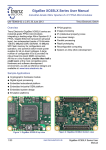
XC6SLX150 X2 Coprocessor
Module User Manual
Issue – 1.0
Foreword
PLEASE READ THIS ENTIRE MANUAL BEFORE PLUGGING IN
OR POWERING UP YOUR XC6SLX150 X2 Coprocessor MODULE.
© Enterpoint Ltd. – XC6SLX150 X 2 Manual – Issue 1.0 7/9/2011
1
PLEASE TAKE SPECIAL NOTE OF THE WARNINGS WITHIN
THIS MANUAL.
Trademarks
Spartan-6, ISE, Webpack, EDK, COREGEN, Xilinx are the registered trademarks of Xilinx Inc,
San Jose, California, US.
Contents
Foreword
Trademarks
Introduction
XC6SLX150 X2 Coprocessor Module
FPGA
CPLD
SPI FLASH
DIL HEADERS
OSCILLATOR
POWER CONNECTIONS
BATTERY
POWER REGULATORS
PROGRAMMING XC6SLX150 X2 Coprocessor Module
MECHANICAL
Medical and Safety Critical Use
Warranty
Support
© Enterpoint Ltd. – XC6SLX150 X 2 Manual – Issue 1.0 7/9/2011
2
2
3
4
6
7
9
11
14
15
17
18
19
23
24
24
24
2
Introduction
The Enterpoint XC6SLX150 X2 Coprocessor Module is a Spartan-6 FPGA based
module offering a highly powerful, flexible and low cost approach to extending the
performance and processing power of our range of development boards. It can be
plugged into our Raggedstone2, Raggedstone3 or Broaddown series boards. It can
also be used as a stand-alone module using its 0.1inch pitch header pins to interface
to a user’s power circuit.
Enterpoint’s Raggedstone2 development board with XC6SLX150 X2 Coprocessor Module
The aim of this manual is to assist in using the main features of the XC6SLX150 X2
Coprocessor Module. There are features that are beyond the scope of the manual.
Should you need to use these features then please email [email protected] for
detailed instructions.
The x 2 Coprocessor Module currently comes with two SLX150-2FGG484C
Spartan-6. Other variants may be offered at a later date or as an OEM product. Please
contact out us on [email protected] should you need further information.
We can offer a PCB design service to interface with this product should you require a
function not covered by our current range of development boards. Typical turn
around for this service is 6-8 weeks depending upon complexity, quantity ordered and
availability of components.
© Enterpoint Ltd. – XC6SLX150 X 2 Manual – Issue 1.0 7/9/2011
3
XC6SLX150 X2 Coprocessor Module
XC6SLX150 X2 Coprocessor Module Front View
XSLX150 x 2 Coprocessor Module Back View
© Enterpoint Ltd. – XC6SLX150 X 2 Manual – Issue 1.0 7/9/2011
4
The XC6SLX150 X2 Coprocessor Module will be supplied un-programmed. You
will need a programming cable to program the XC6SLX150 X2 Coprocessor Module
– for example the Enterpoint Prog2 parallel port programming cable or the Enterpoint
Prog3 USB port programming cable. You will also need a programming adapter for
the Enterpoint programming cables because the JTAG connector on the module is a
6x2 1.27mm header.
The Xilinx toolset required to program the XC6SLX150 X2 Coprocessor Module
depends upon the Spartan6 devices fitted to the board.
If your XC6SLX150 X2 Coprocessor Module is fitted with LX150 devices (standard
version) it will require the full Xilinx toolset to build a design. If you have a custom
version fitted with an LX75 device or smaller it is supported by the free ISE
Webpack. ISE Version11.1 SP4 or later is required, available from Xilinx. This
provides all the tools to enter and build a design. Using this tool in conjunction with
your programming cable you will also be able to program the Spartan-6s, and the
supporting SPI Flash, that are on the XC6SLX150 X2 Coprocessor Module.
ISE Webpack can be obtained directly from the Xilinx website at
http://www.xilinx.com/ise. Registration will be necessary to complete the download.
The full ISE toolset can also be purchased from the Xilinx website.
© Enterpoint Ltd. – XC6SLX150 X 2 Manual – Issue 1.0 7/9/2011
5
FPGAs
The XC6SLX150 X2 Coprocessor Module supports Spartan-6 devices in the
FGG484 package. This module is normally available with commercial grade -2 speed
devices fitted in the XC6SLX150 size. Should you have an application that needs a
different size of FPGA, industrial specification parts or faster speed grades please
contact sales for a quote at [email protected].
The FPGA PROG_B, CSO_B, INIT_B, DONE and M[0:1] signals are routed to the
CPLD and can be routed from the CPLD to the DIL header pins if required so that
configuration of the FPGAs can be controlled by a host board. Similarly the CSO_B
signals from the SPI flash memory devices are routed to the CPLD. Some of these
signals require pullup resistors to be implemented in the CPLD program.
The FPGAs are interconnected by 38 routes which are shown below:
FPGA1 PIN
FPGA2 PIN
FPGA1 PIN
FPGA2 PIN
1
T2
T21
20
H1
H22
2
T1
T22
21
G3
G20
3
R3
R20
22
G1
G22
4
R1
R22
23
F2
F21
5
P2
P21
24
F1
F22
6
P1
P22
25
E3
E20
7
N3
N20
26
E1
E22
8
N1
N22
27
D2
D21
9
M2
M21
28
D1
D22
10
M1
M22
29
C3
C20
11
L3
L20
30
C1
C22
12
L1
L22
31
B2
B21
13
K2
K21
32
B1
B22
14
K1
K22
33
U3
U20
15
J3
J20
34
U1
U22
16
J1
J22
35
V2
V21
17
M3
M20
36
V1
V22
18
L4
L19
37
W3
W20
19
H2
H21
38
W1
W22
© Enterpoint Ltd. – XC6SLX150 X 2 Manual – Issue 1.0 7/9/2011
6
CPLD
The XC6SLX150 X2 Coprocessor Module has an XC9572XL-10VQG64 CPLD
which can be used to control the FPGA configuration signals or to route these signals
to a host board so that they can be controlled externally. This latter option enables a
host board to initiate reconfiguration of the FPGAs on the XC6SLX150 X2
Coprocessor Module. The JTAG signals are also available to be routed from the
CPLD to the DIL headers if required. A suitable build must be loaded into the CPLD
before the FPGAs will configure from their SPI flash memory devices.
There are 8 Control signals which connect between the CPLD and 8 of the DIL
header pins. The connections to the CPLD are shown below:
CPLD
PIN
SIGNAL NAME
CONNECTS TO
CPLD
PIN
SIGNAL NAME
CONNECTS TO
1
CSO_SPI_1_N
SPI1 FLASH P1
47
DONE_FPGA1
FPGA1 PIN Y22
10
TMS_DR
TMS
49
CSO_B_FPGA2
FPGA2 PIN T5
11
TDI_DR
TDI
50
INIT_B_FPGA1
FPGA1 PIN T6
12
TDO_DR
TDO
51
M1_FPGA2
FPGA2 PIN U15
13
TCK_DR
TCK
52
INIT_B_FPGA2
FPGA6 PIN T6
15
CLOCK_25MHZ
OSCILLATOR
56
PROG_B_FPGA2
FPGA2 PIN AA1
16
CSO_SPI_2_PIN_N
LHS PIN 15
57
PROG_B_FPGA1
FPGA1 PIN AA1
22
CONTROL5
LHS PIN 1
58
CSO_SPI_1_PIN_N
RHS PIN 15
24
CONTROL6
LHS PIN 2
59
M0_FPGA2
FPGA2 PIN AA22
25
CONTROL7
LHS PIN 3
60
DONE_FPGA2
FPGA2 PIN Y22
27
CONTROL8
LHS PIN 4
61
CONTROL4
RHS PIN 4
31
CSO_SPI_2_N
SPI2 FLASH P1
62
CONTROL3
RHS PIN 3
39
CSO_B_FPGA1
FPGA1 PIN T5
63
CONTROL2
RHS PIN 2
45
M1_FPGA1
FPGA1 PIN U15
64
CONTROL1
RHS PIN 1
46
M0_FPGA1
FPGA1 PIN AA22
In order to enable each FPGA to configure from its SPI Flash memory device at
startup it is necessary to set M0 high, M1 low, PROG_B high and to route each
CSO_B signal from the SPI flash device to the CSO_B pin of its FPGA ie link from
pin 1(output) to pin 39(input) and pin 31(output) to pin 49(input). The DONE and
INIT_B signals on each FPGA are pulled up by fixed resistors. The following VHDL
code achieves this:
© Enterpoint Ltd. – XC6SLX150 X 2 Manual – Issue 1.0 7/9/2011
7
LIBRARY IEEE;
USE IEEE.STD_LOGIC_1164.ALL;
USE IEEE.STD_LOGIC_ARITH.ALL;
USE IEEE.STD_LOGIC_UNSIGNED.ALL;
ENTITY TOPLEVEL IS
PORT(
CSO_B_FPGA1
:
CSO_B_FPGA2
:
CSO_SPI_1_N
:
CSO_SPI_2_N
:
M0_FPGA1
:
M0_FPGA2
:
M1_FPGA1
:
M1_FPGA2
:
PROG_B_FPGA1
:
PROG_B_FPGA2
:
);
IN
IN
OUT
OUT
OUT
OUT
OUT
OUT
OUT
OUT
STD_LOGIC;
STD_LOGIC;
STD_LOGIC;
STD_LOGIC;
STD_LOGIC;
STD_LOGIC;
STD_LOGIC;
STD_LOGIC;
STD_LOGIC;
STD_LOGIC
-- CS FROM FPGA1
-- CS FROM FPGA2
-- CS TO SPI FLASH 1
-- CS TO SPI FLASH 2
END TOPLEVEL;
ARCHITECTURE A0 OF TOPLEVEL IS
BEGIN
M0_FPGA1
M0_FPGA2
M1_FPGA1
M1_FPGA2
<= '1';
<= '1';
<= '0';
<= '0';
CSO_SPI_2_N <= CSO_B_FPGA2;
CSO_SPI_1_N <= CSO_B_FPGA1;
PROG_B_FPGA1 <= '1';
PROG_B_FPGA2 <= '1';
END A0 ;
In order to route the JTAG signals to the DIL headers (Right hand side
pins 1 to 4) the following lines will need to be added:
Add to the PORT declaration:
TMS
TCK
TDO
TDI
:
:
:
:
OUT
OUT
IN
OUT
STD_LOGIC;
STD_LOGIC;
STD_LOGIC;
STD_LOGIC;
CONTROL1
CONTROL2
CONTROL3
CONTROL4
: IN
STD_LOGIC;
: OUT STD_LOGIC;
: IN
STD_LOGIC;
: IN
STD_LOGIC;
Add to the Architecture:
TCK
CONTROL2
TDI
TMS
<= CONTROL1;
<= TDO;
<= CONTROL3;
<= CONTROL4;
-- PIN1 HAS THE TCK SIGNAL
-- PIN 2 HAS THE TDO SIGNAL
-- PIN 3 HAS THE TDI SIGNAL
-- PIN4 HAS THE TMS SIGNAL
© Enterpoint Ltd. – XC6SLX150 X 2 Manual – Issue 1.0 7/9/2011
8
SPI FLASH MEMORY
The XC6SLX150 X2 Coprocessor Module maybe fitted with either the
Micron/Numonyx M25P128 or the Winbond 25Q128BV SPI flash memory device.
The M25P128 will operate in single bit wide mode, whereas the Winbond
25Q128BV can operate in single, dual or quad modes. The SPI flash devices
configure the FPGAs when the module is powered up provided a suitable bitstream
(.mcs file) is programmed into the device. Each device has a capacity of 128Mbits
with a single configuration bitstream each XC6SLX150 taking 4.1Mbits. Any
remaining space can be used for alternative configurations or code and data storage.
For further information concerning these flash memory devices please consult
www.micron.com or www.winbond.com.
The SPI flash memory signals are routed to the DIL headers on the pins shown in the
table below so that the devices can be accessed from a host board. The SPI flash for
FPGA1 routes to the right side header pins, the SPI flash for FPGA2 routes to
the left side header pins.
© Enterpoint Ltd. – XC6SLX150 X 2 Manual – Issue 1.0 7/9/2011
9
After the FPGAs have configured each SPI Flash can be accessed via the following
pins of the FPGA.
SPI FLASH
FUNCTION
CCLK
DOUT
WRITE
DIN
CSO_B*
HOLD
FPGA PIN
HEADER PIN
Y21
AB20
U9
AA20
T5
U13
19
20
16
17
15
18
*The flash device CSO_B signal is routed to the CPLD and must be routed to this pin
by a suitable build in the CPLD.
The flash memory can be programmed directly via the JTAG interface (see section
below “PROGRAMMING XC6SLX150 X2 Coprocessor Module”) or from the host
board.
© Enterpoint Ltd. – XC6SLX150 X 2 Manual – Issue 1.0 7/9/2011
10
DIL HEADERS
The DIL Headers provide a simple mechanical and electrical interface for connection
to the module. There are twenty I/O on the left side of the module 20 IO on the right
hand side of the module giving a total of 40 I/O available. A further 8 IO are routed
from the DIL header pins to the CPLD. (Control[1:8]). The maximum signal voltage
on the GPIO is 3.3v.
The DIL Headers can support 20 pairs of LVDS signalling. The Spartan-6 FPGA can
terminate any of these pairs. LVDS termination on individual signal pairs is a
programmable option that can be set in build constraints for the FPGA when using
the ISE toolset. The LVDS pairs are shown in the table below along with FPGA pin
numbers.
© Enterpoint Ltd. – XC6SLX150 X 2 Manual – Issue 1.0 7/9/2011
11
The DIL Headers will also support the use of crude prototype circuits using
stripboard or other prototype materials. The DIL Header connectors are arranged on a
standard 0.1inch (2.54mm) pitch. The horizontal pitch of the DIL Headers is 1.6
inches between the outer rows of the headers. The inner pins of the header form
continuous power strips. The right hand side header has an inner column of 3.3V
pins. The LHS header has an inner column of DGND (0V).
ROW
1
2
3
4
5
6
7
8
9
10
11
12
13
14
15
16
17
18
19
20
21
22
23
24
25
26
27
28
29
30
LEFT COLUMN
OUTER PINS
FUNCTION
S6 PIN
CONTROL5
CONTROL6
CONTROL7
CONTROL8
IO_L34P_0 FPGA1
IO_L34N_0 FPGA1
IO_L8P_0 FPGA1
IO_L8N_0 FPGA1
IO_L6P_0 FPGA1
IO_L6N_0 FPGA1
IO_L5P_0 FPGA1
IO_L5N_0 FPGA1
IO_L4P_0 FPGA1
IO_L4N_0 FPGA1
CSO_SPI_2_PIN_N
WRITE_2
DIN_FLASH2
DOUT_FLASH2
CCLK_FLASH2
HOLD_2
IO_L37P_0 FPGA2
IO_L37N_0 FPGA2
IO_L35P_0 FPGA2
IO_L35N_0 FPGA2
IO_L34P_0 FPGA2
IO_L34N_0 FPGA2
IO_L8P_0 FPGA2
IO_L8N_0 FPGA2
IO_L6P_0 FPGA2
IO_L6N_0 FPGA2
CPLD 22
CPLD 24
CPLD 25
CPLD 27
B10
A10
C9
A9
B8
A8
C7
A7
B6
A6
CPLD 16
U14
AA20
AB20
Y21
U13
B12
A12
C11
A11
B10
A10
C9
A9
B8
A8
INNER
PINS
0V
0V
0V
0V
0V
0V
0V
0V
0V
0V
0V
0V
0V
0V
0V
0V
0V
0V
0V
0V
0V
0V
0V
0V
0V
0V
0V
0V
0V
0V
INNER
PINS
3.3V
3.3V
3.3V
3.3V
3.3V
3.3V
3.3V
3.3V
3.3V
3.3V
3.3V
3.3V
3.3V
3.3V
3.3V
3.3V
3.3V
3.3V
3.3V
3.3V
3.3V
3.3V
3.3V
3.3V
3.3V
3.3V
3.3V
3.3V
3.3V
3.3V
RIGHT COLUMN
OUTER PINS
FUNCTION
S6 PIN
CONTROL1
CONTROL2
CONTROL3
CONTROL4
IO_L14P_2 FPGA1
IO_L14N_2 FPGA1
IO_L48P_2 FPGA1
IO_L48N_2 FPGA1
IO_L49P_2 FPGA1
IO_L49N_2 FPGA1
IO_L57N_2 FPGA1
IO_L57N_2 FPGA1
IO_L64N_2 FPGA1
IO_L64N_2 FPGA1
CSO_SPI_1_PIN_N
WRITE_1
DIN_FLASH1
DOUT_FLASH1
CCLK_FLASH1
HOLD_1
IO_L31P_2 FPGA2
IO_L31P_2 FPGA2
IO_L32P_2 FPGA2
IO_L32P_2 FPGA2
IO_L41P_2 FPGA2
IO_L41N_2 FPGA2
IO_L43P_2 FPGA2
IO_L43N_2 FPGA2
IO_L45P_2 FPGA2
IO_L45N_2 FPGA2
CPLD 64
CPLD 63
CPLD 62
CPLD 61
AA18
AB18
Y7
AB7
AA6
AB6
AA4
AB4
AA2
AB2
CPLD 58
U14
AA20
AB20
Y21
U13
AA12
AB12
Y11
AB11
AA10
AB10
Y9
AB9
AA8
AB8
It should be noted that the pins on the XC6SLX150 X2 Coprocessor Module should
be treated with respect. The XC6SLX150 X2 Coprocessor Module is usually supplied
with an extra row of pin-socket headers to protect the row of pins which are soldered
into the board. This means that if a pin is broken this extra row of headers can be
© Enterpoint Ltd. – XC6SLX150 X 2 Manual – Issue 1.0 7/9/2011
12
replaced easily and cheaply. Enterpoint can supply extra pins-socket headers if
required. Contact [email protected]. Enterpoint does not accept
responsibility if the header pins on the module have been damaged due to poor
handling.
© Enterpoint Ltd. – XC6SLX150 X 2 Manual – Issue 1.0 7/9/2011
13
OSCILLATOR
The oscillator on the XC6SLX150 X2 Coprocessor Module is an ASEM 25MHz
oscillator. The oscillator is situated as shown below and is connected to each FPGA
on PIN AB13.
The Spartan-6 has PLLs and DCMs to produce multiples, divisions and phases of the
clock for specific application requirements. Please consult the Spartan-6 datasheet
available from the Xilinx website at http://www.xilinx.com if multiple clock signals
are required.
© Enterpoint Ltd. – XC6SLX150 X 2 Manual – Issue 1.0 7/9/2011
14
POWER CONNECTIONS
The XC6SLX150 X2 Coprocessor Module requires input voltages of 5v and 3.3v in
order to operate. 3.3V must be connected to the inner right row of header pins as
shown below:
The user can supply 3.3v to the module on any or all of the right hand side inner
header pins and 0V on any or all of the left hand side inner header pins. This can be
achieved by plugging the module into the Enterpoint Raggedstone2 or 3 or
Broaddown series development boards, which all have sockets with appropriate
power connections for this module and resettable fuses to limit the current. A user
can also provide 3.3V and 0V from another source onto these pins. The pins are
arranged on a 0.1inch pitch (2.54mm) to facilitate this. The horizontal distance
between the 0V pins and the 3.3V pins in 1.4inches.
© Enterpoint Ltd. – XC6SLX150 X 2 Manual – Issue 1.0 7/9/2011
15
The 5v feed is used to generate the 1.2V core voltage for the FPGAs. There are 2
options for supplying 5V to the XC6SLX150 X2 Coprocessor Module.
There is a 4-pin connector on the module which accepts connectors usually seen in
PCs to connect power to HDD or CD/DVD drives. The pinout of the connector suits
these connectors and the module requires 5v and 0v. The 4th terminal, usually 12v in
a PC, is unconnected on the module. Care should be taken not to exceed 5V input
as this can cause damage to the XC6SLX150 X2 Coprocessor Module. The
module is protected by a 2.6A resettable fuse on the 5v feed.
Alternatively the 3.3V supply can be used to supply power for the FPGA core
voltage. It should be noted that if a demanding build is loaded into the FPGAs the
current drawn by the module may exceed the fuse rating on the host board. If this
option is chosen it is necessary to connect a zero ohm link on the back of the
XC6SLX150 X2 Coprocessor Module (see below). If you subsequently use the 5v
input connector you must remember to remove this zero ohm link. Extreme care
should be taken when soldering to the back of the module Enterpoint Ltd will
not accept responsibility for damage to the module due to poor soldering
technique. Care should be taken not to exceed 3.3v input as this can cause
damage to the XC6SLX150 X2 Coprocessor Module.
© Enterpoint Ltd. – XC6SLX150 X 2 Manual – Issue 1.0 7/9/2011
16
BATTERY
A battery holder is supplied on the underside of the XC6SLX150 X2 Coprocessor
Module that can take a nominal 4.8mm diameter, 1.5mm thick rechargeable coin cell
battery providing 1V to 3.6V e.g Panasonic ML414S/ZT. We do not normally supply
the battery to avoid shipping issues with batteries. It is connected to pin R17 of the
FPGAs and recharges from the 3.3V supply. VBATT is required to maintain the
battery backed RAM AES key when VCCAUX is not applied to the FPGA.
© Enterpoint Ltd. – XC6SLX150 X 2 Manual – Issue 1.0 7/9/2011
17
POWER REGULATORS
The XC6SLX150 X2 Coprocessor Module has one voltage regulators supplying
1.2V.
WARNING – REGULATORS CAN BECOME HOT IN NORMAL
OPERATION ALONG WITH THE BOARDS THERMAL RELIEF. PLEASE
DO NOT TOUCH OR PLACE HIGHLY FLAMABLE MATERIALS NEAR
THESE DEVICES WHILST THE XC6SLX150 X2 Coprocessor MODULE IS
IN OPERATION.
A Micrel MIC22950 regulator supplies 1.2V with a maximum current available of
10A. This is used for the core voltage of the FPGAs.
© Enterpoint Ltd. – XC6SLX150 X 2 Manual – Issue 1.0 7/9/2011
18
Programming XC6SLX150 X2 Coprocessor Module
The programming of the FPGA and SPI Flash parts on the XC6SLX150 X2
Coprocessor Module is achieved using the JTAG interface. The JTAG connector on
the XC6SLX150 X2 Coprocessor Module is a 1.27mm pitch 6x2 header and will
require an adapter to be used with standard Enterpoint or Xilinx programming cables.
The pinout of the JTAG connector is shown below:
Top layer PCB trackwork showing JTAG connector pinout
The JTAG signals are routed to the following pins on the CPLD. These signals can be
routed to pins on the DIL headers by loading a suitable build into the CPLD if you
wish to program the Coprocessor module from the host board.
JTAG SIGNAL
CPLD PIN
TDI
11
TDO
12
TCK
13
TMS
10
The Spartan-6 series needs to be programmed using ISE 11 or higher. Versions of
ISE prior to 11 do not support Spartan-6. The full version of the Xilinx tools is
required to program the XC6SLX150-2FGG484C. The free Webpack version of ISE
is sufficient to support the smaller versions of the FPGA.
There is a single JTAG chain on the XC6SLX150 X2 Coprocessor Module. The
JTAG chain allows the programming of the CPLD, both Spartan-6s and the two SPI
Flash memory devices.
© Enterpoint Ltd. – XC6SLX150 X 2 Manual – Issue 1.0 7/9/2011
19
Using iMPACT Boundary Scan the JTAG chain appears like this:
JTAG chain following Boundary scan
The first device is the CPLD, the second is FPGA1, the third is FPGA2.
1. Programming the CPLD
The xc9572xl CPLD has its own internal storage for configuration data. Use your
programming tools to generate a suitable ‘jed file to achieve your desired
functionality. Right-click the the icon representing the Spartan-6 FPGA and choose
‘Assign New Configuration File’. Navigate to your .jed file and choose ‘OPEN’. The
.jed file name will appear under the CPLD as shown below:
JTAG chain with configuration files assigned
Right click the icon representing the CPLD and choose ‘Program’. Depending on
your version of iMPACT you may need to respond to a programming properties
dialogue box by clicking OK. The Spartan-6 will program. This process is very quick
(typically a few seconds).
2. Programming the FPGAs directly.
Direct JTAG programming of the Spartan-6 FPGAs is volatile and the FPGAs will
lose their configuration every time the board power is cycled. For sustained use of an
FPGA design programming the design into the Flash memory is recommended (see 2
and 3 below).
Direct JTAG programming using .bit files is useful for fast, temporary programming
during development of FPGA programs. Right click the icon representing the
© Enterpoint Ltd. – XC6SLX150 X 2 Manual – Issue 1.0 7/9/2011
20
Spartan-6 FPGA and choose ‘Assign New Configuration File’. Navigate to your .bit
file and choose ‘OPEN’. The next dialogue box will offer to add a flash memory and
you should decline. Right click the icon representing the Spartan-6 FPGA and choose
‘Program’. On the next dialogue box ensure that the ‘Verify’ box is not checked. (If it
is you should uncheck it, failure to do this will result in error messages being
displayed). Click OK. The Spartan-6 will program. This process is very quick
(typically a few seconds)
3. Programming the SPI flash memory using Boundary Scan.
Once the SPI Flash memories have been programmed, the Spartan-6 devices will
automatically load from the Flash memories at power up. Generation of suitable
Flash memory files (.mcs) can be achieved using ISE iMPACT’s Prom File
Formatter.
Right click on the icon representing each Spartan-6 and choose ‘Add SPI/BPI Flash’
Navigate to your programming file (.mcs) and click OPEN. Use the next dialogue
box to select SPI flash and M25P128 or W25Q128BV. Data width should be set
appropriately. The flash memories should appear as shown below.
JTAG chain with configuration files assigned and SPI Flash memory added
Right click on the icon representing each flash memory and choose ‘Program’ to load
your programs into the devices. It is recommended that options to ‘Verify’ and ‘Erase
before programming’ are chosen. Otherwise all defaults can be accepted. The
programming operation will take some time (at least 3 or 4 minutes per device).
Depending upon the memory device and the settings used when generating the
bitfiles using ISE, it will take up to 20 seconds for an XC6LX150 to configure upon
power-up. In order to decrease this time the following process can be followed:
1. In the main ISE menu, right-click ‘Generate Programming file’. Choose
Properties.
2. On the left hand side of the Process Properties Dialogue box, choose
Configuration Options.
© Enterpoint Ltd. – XC6SLX150 X 2 Manual – Issue 1.0 7/9/2011
21
3. The first item on the menu which appears on the right hand side of the dialogue
box is ‘Configuration Rate’. The default setting is 2. Increase this number. The
maximum value we suggest is 22. Choose ‘Apply’ and ‘OK’.
4. Generate the program file as normal.
© Enterpoint Ltd. – XC6SLX150 X 2 Manual – Issue 1.0 7/9/2011
22
MECHANICAL ARRANGEMENT
The Dimensions on the drawings below are millimetres (mm). All sizes quoted are
subject to manufacturing tolerances and should only be used as a general guide.
The socket pins on the DIL headers are arranged on a 2.45mm (0.1inch) pitch
The maximum height of the components on the upper side of the module, measured
from the lower surface of the PCB is less than 10mm.
When the XC6SLX150 X2 Coprocessor Module is plugged into a Raggedstone2
development board using doubled header pins the total height from the underside of
the Raggedstone2 to the top of the XC6SLX150 X2 Coprocessor Module components
is approximately 25mm.
© Enterpoint Ltd. – XC6SLX150 X 2 Manual – Issue 1.0 7/9/2011
23
Medical and Safety Critical Use
XC6SLX150 X2 Coprocessor Modules are not authorised for the use in, or use in the
design of, medical or other safety critical systems without the express written person
of the Board of Enterpoint. If such use is allowed the said use will be entirely the
responsibility of the user. Enterpoint Ltd accepts no liability for any failure or defect
of the XC6SLX150 X2 Coprocessor Module, or its design, when it is used in any
medical or safety critical application.
Warranty
The XC6SLX150 X2 Coprocessor Module comes with a 90 day return to base
warranty. Do not attempt to solder connections to the XC6SLX150 X2 Coprocessor
Module. Enterpoint reserves the right not honour a warranty if the failure is due to
soldering or other maltreatment of the XC6SLX150 X2 Coprocessor Module.
Outside warranty Enterpoint offers a fixed price repair or replacement service. We
reserve the right not to offer this service where a XC6SLX150 X2 Coprocessor
Module has been maltreated or otherwise deliberately damaged. Please contact
support if you need to use this service.
Other specialised warranty programs can be offered to users of multiple Enterpoint
products. Please contact sales on [email protected] if you are interested in
these types of warranty,
Support
Please check our online FAQ page for this product first before contacting support.
Telephone and email support is offered during normal United Kingdom working
hours (GMT or GMT + 1) 9.00am to 5.00pm.
Telephone - +44 (0) 121 288 3945
Email
- [email protected]
© Enterpoint Ltd. – XC6SLX150 X 2 Manual – Issue 1.0 7/9/2011
24