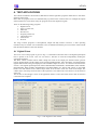
1
INTECO Krakow, POLAND, [email protected] www.inteco.com.pl RT-DAC/USB2 I/O Board Board version 1.03 User’s Manual Kraków 2010 Revision History Version 1.0 1.1 Date 2010-09-30 2010-10-25 Resp. KK KK Description First release Text improvements InTeCo Table of contents 1. GENERAL INFORMATION................................................................................................................. 4 1.1 1.2 SPECIFICATION ................................................................................................................................... 4 BOARD ARCHITECTURE ...................................................................................................................... 6 2. BOARD INSTALLATION ..................................................................................................................... 7 3. DRIVER INSTALLATION.................................................................................................................... 8 4. CONNECTOR PIN ASSIGNMENT.................................................................................................... 10 5. USB ACCESS FUNCTIONS ................................................................................................................ 14 5.1 GENERAL DESCRIPTION OF SOFTWARE INTERFACES ......................................................................... 14 5.1.1 C interface ............................................................................................................................... 14 5.1.2 .NET interface.......................................................................................................................... 15 5.1.3 MATLAB/Simulink interface.................................................................................................... 16 5.2 USB FUNCTIONS .............................................................................................................................. 18 5.2.1 C interface ............................................................................................................................... 18 5.2.2 .NET interface.......................................................................................................................... 21 5.3 VERSION MANAGEMENT ................................................................................................................... 23 5.3.1 Logic version ........................................................................................................................... 23 5.3.2 Application name..................................................................................................................... 23 5.3.3 Synthesis date .......................................................................................................................... 23 5.3.4 Number of channels ................................................................................................................. 24 5.3.5 Example ................................................................................................................................... 24 5.4 OPERATING MODE OF THE SHARED OUTPUT SIGNALS ....................................................................... 26 5.5 DIGITAL I/O ..................................................................................................................................... 27 5.5.1 Direction.................................................................................................................................. 27 5.5.2 Input......................................................................................................................................... 28 5.5.3 Output...................................................................................................................................... 28 5.5.4 Example ................................................................................................................................... 29 5.6 COUNTER/TIMER .............................................................................................................................. 31 5.6.1 Mode........................................................................................................................................ 31 5.6.2 Reset ........................................................................................................................................ 32 5.6.3 Counter .................................................................................................................................... 32 5.6.4 Example ................................................................................................................................... 33 5.7 PWM ............................................................................................................................................... 35 5.7.1 Mode........................................................................................................................................ 36 5.7.2 Prescaler.................................................................................................................................. 36 5.7.3 Width ....................................................................................................................................... 36 5.7.4 Example ................................................................................................................................... 37 5.8 ENCODER ......................................................................................................................................... 39 5.8.1 Reset ........................................................................................................................................ 40 5.8.2 IdxActive .................................................................................................................................. 40 5.8.3 IdxInvert .................................................................................................................................. 41 5.8.4 Counter .................................................................................................................................... 41 5.8.5 Example ................................................................................................................................... 41 5.9 FREQUENCY METER .......................................................................................................................... 43 5.9.1 EnableBlock............................................................................................................................. 44 5.9.2 SwHwGateStartFlag ................................................................................................................ 44 5.9.3 SwStart..................................................................................................................................... 45 5.9.4 StartInv .................................................................................................................................... 45 5.9.5 SwGate..................................................................................................................................... 45 5.9.6 GateInv .................................................................................................................................... 45 5.9.7 InputInv.................................................................................................................................... 46 RT-DAC/USB2 - User’s Manual page 1 InTeCo 5.9.8 GateMode ................................................................................................................................ 46 5.9.9 InfiniteFlag .............................................................................................................................. 46 5.9.10 Mode........................................................................................................................................ 47 5.9.11 Timer ....................................................................................................................................... 47 5.9.12 Ready ....................................................................................................................................... 47 5.9.13 Counter .................................................................................................................................... 48 5.9.14 Result ....................................................................................................................................... 48 5.9.15 Example ................................................................................................................................... 48 5.10 CHRONOMETER ................................................................................................................................ 51 5.10.1 EnableBlock............................................................................................................................. 52 5.10.2 TriggerMode............................................................................................................................ 53 5.10.3 EnableGate .............................................................................................................................. 53 5.10.4 InvertStartStop......................................................................................................................... 53 5.10.5 InvertStop ................................................................................................................................ 53 5.10.6 InvertGate................................................................................................................................ 54 5.10.7 ArmMeasurement..................................................................................................................... 54 5.10.8 NextMeasurement .................................................................................................................... 54 5.10.9 Armed ...................................................................................................................................... 55 5.10.10 Pending................................................................................................................................ 55 5.10.11 Ready ................................................................................................................................... 55 5.10.12 ClkDivider ........................................................................................................................... 55 5.10.13 Counter ................................................................................................................................ 56 5.10.14 Result ................................................................................................................................... 56 5.10.15 Example ............................................................................................................................... 57 5.11 A/D CONVERSION ............................................................................................................................. 59 5.11.1 Gain ......................................................................................................................................... 59 5.11.2 Result ....................................................................................................................................... 59 5.11.3 Example ................................................................................................................................... 60 5.12 D/A CONVERSION ............................................................................................................................. 62 5.12.1 D/A control .............................................................................................................................. 62 5.12.2 Example ................................................................................................................................... 63 6. TEST APPLICATIONS........................................................................................................................ 64 6.1 6.2 6.3 6.4 6.5 6.6 6.7 6.8 DIGITAL IO TEST .............................................................................................................................. 64 TIMER/COUNTER TEST...................................................................................................................... 65 PWM TEST ....................................................................................................................................... 66 ENCODER TEST ................................................................................................................................. 67 FREQUENCY METER TEST ................................................................................................................. 67 CHRONOMETER TEST ........................................................................................................................ 69 A/D CONVERSION TEST .................................................................................................................... 71 D/A CONVERSION TEST .................................................................................................................... 72 RT-DAC/USB2 - User’s Manual page 2 InTeCo NOTES MATLAB, Simulink, RTW and RTWT are registered trademarks of The MathWorks, Inc. Windows 95/98/NT/2000/XP are registered trademarks of Microsoft Corporation Copyright INTECO 2010. All rights reserved. RT-DAC/USB2 - User’s Manual page 3 InTeCo 1. GENERAL INFORMATION The RT-DAC/USB2 is a multifunction analog and digital I/O board dedicated to real-time data acquisition and control in the Windows 95/98/NT/2000/XP environments. The board contains a Xilinx FPGA chip. All boards are built as the OMNI version. It means the boards can be reconfigured to introduce a new functionality of all inputs and outputs without any hardware modification. The default configuration of the FPGA chip accepts signals from incremental encoders and generates PWM outputs, typical for mechatronic control applications and is equipped with the general purpose digital input/outputs (GPIO), A/D and D/A converters, timers, counters, frequency meters and chronometers. The RT-DAC/USB2 board is distributed in two versions: • analog and digital (RT-DAC/USB2) and • digital only (RT-DAC/USB2-D). This manual contains description for the both versions. In the case, if any facility of the board relates to one version only, this fact is clearly marked. 1.1 Specification Analog section (not available in the RT-DAC/USB2-D version) Analog Inputs Channels: Resolution: Input ranges: Conversion time: Trigger: Reference voltage: Analog Outputs Channels: Resolution: Output range: Settling time: Reference voltage: 16 single-ended, multiplexed 12 bit ±10V, programmable gain (x1, x2, x4, x8, x16) 5.4 µs all the A/D channels are scanned automatically when USB host requires data on-board 4 12 bit / 14 bit ± 10V, ± 5V 10 µs (to 0.01%) on-board Digital section (version 1.03) Digital Input/ Output Channels: Direction: Input voltage: Output voltage: Output current: Standard: Digital Timer/Counter 32 bit timer / counter : RT-DAC/USB2 - User’s Manual 26 bi-directional, direction setting; 8 channels shared with PWM outputs; some inputs shared with counter, timer, chronometer and frequency meter inputs bi-directional, individually software programmable VIH = 2.0V÷3.6V, VIL = - 0.5V÷0.8V VOH = 2.4V (min), VOL = 0.4V (max) 2mA per channel LVTTL 2 channels, counts internal clock signal or external impulses . External pulse duration: min 50ns page 4 InTeCo PWM Outputs Channels: Resolution: Base frequency: Incremental encoders Channels: Output: Index 4 8/12 bits (software selected) programmable, initial 16-bits divider 4 32 bit counter Software configured. 2 modes: with and without index, selectable active level of the index signal USB features USB 2.0 hi-speed specification compliant. RT-DAC/USB2 - User’s Manual page 5 InTeCo 1.2 Board architecture The block diagram of the RT-DAC/USB2 board is shown in Fig. 1.1. The block diagram of the digital version is presented in Fig. 1.2. Clock reference signal digital I/O PWM encoders USB /FPGA XILINX FPGA bridge timer/counter frequency meter chronometer Configuration USB Interface Programmable gain 16 channels A/D converter EEPROM D/A converters D/A buffers USB Bus Fig. 1.1. General block diagram of the RT-DAC/USB2 board Clock reference signal digital I/O PWM encoders USB /FPGA XILINX FPGA bridge timer/counter frequency meter chronometer Configuration USB Interface EEPROM USB Bus Fig. 1.2. General block diagram of the RT-DAC/USB2-D board The board is equipped with the 12-bit successive approximation A/D converters that give the 5 mV resolution within the input range ±10V. A finer resolution can be achieved by the gain definition using digitally programmable analog amplifier. The A/D conversion time of the RT-DAC/USB2 board is equal to 5.4 µs. The board contains four 12-bits D/A converters connected to four analog output channels (optionally 14-bit D/A converters are available). The output voltage of the channels is ± 10V. Each analog output channel can sink up to 10 mA. Reprogramming the XILINX FPGA chip at the boards can change functions of the board. The information and specification how to reprogram XILINX FPGA is not included in this guide. Please, relate to RTDAC/USB2 FPGA Programming Guide distributed by INTECO separately. RT-DAC/USB2 - User’s Manual page 6 InTeCo 2. BOARD INSTALLATION The RT-DAC/USB2 setup contains: • • • • • • RT-DAC/USB2 board, Two 40-pin ribbon cables (only one cable when the digital version is distributed ), USB cable, CD containing a software and e-manuals, terminal wiring board (optional), 9V-12V DC / 4W stabilised power supply (optional). The plug dimensions are given in Fig. 2.2. The layout of the RT-DAC/USB2 board is presented in Fig. 2.1 RT-DAC/USB2 USB socket Power socket LEDs: Power Programming enable Ready CN2 and CN1 40-pins connectors (CN1 not visible) metal part φ 5.5 mm min 13 mm On/Off Fig. 2.1. The layout of the RT-DAC/USB2 board Fig. 2.2. The plug of the DC power supply The CN1 connector is not visible at the Fig. 2.1 because it is placed below the CN2 connector. The digital version of the board is equipped with the CN1 connector only. The CN2 connector contains pins connected to A/D inputs and D/A outputs only. The Power signalling LED is emitting light when the On/Off switch is on, Ready LED indicates that the communication between the RT-DAC/USB2 board and computer is running and Programming Enable LED is emitting light when the board is ready to be programmed. To install the board: • install driver for the board (see below or CD:\DRIVER\readme*.txt), • install RT-DAC/USB2 testing applications • optionally install the RT-CON package, • connect the board to the computer using the included USB cable, • connect the national version of the DC 9V-12V stabilised power supply (not included). 9V DC voltage is recommended. • test the board (see section 6). RT-DAC/USB2 - User’s Manual page 7 InTeCo 3. DRIVER INSTALLATION The driver for RT-DAC/USB2 board has to be installed. The user with administrator privileges must install the drivers for Windows 2000 and Windows XP. Windows 2000/XP installation 1. 2. 3. 4. Start Microsoft Windows 2000/XP Connect the RT-DAC/USB2 device and turn power ON System detects a new USB device Select the file CD:\driver\w2k_xp\cyusb.inf and then press OK If the driver is not installed and the RT-DAC/USB2 device is connected to the PC it appears as unknown device at the list of the devices in the Device Manager (see Fig. 3.1). Fig. 3.1. Device list with an unknown device Fig. 3.2. Update driver option Press the right mouse button at the Unknown device item and select the Update Driver Software item (see Fig. 3.2). Select the Browse my computer for driver software option (DO NOT select the Search automatically for updated driver software) and select the driver location as given in Fig. 3.3and Fig. 3.4. Fig. 3.3. Browse the computer option Fig. 3.4. Select the driver Windows displays the security warning caused by the uncertified driver. Please force the driver to be installed (see Fig. 3.5). Finally the confirmation of the successful driver installation is given as presented in Fig. 3.6. RT-DAC/USB2 - User’s Manual page 8 InTeCo Fig. 3.5. Windows security warning Fig. 3.6. Confirmation of the successful installation The 64-bit versions of Windows require that all drivers are digitally certified, which the driver for the RT_DAC/USB2 is not. A user needs to reboot the Windows PC and press F8 to show the boot option list. The loading/installing unsigned drivers option has to be selected to allow installation of the driver. When the RT-DAC/USB2 is properly installed it is visible in the Device Manager at the list of devices in the Universal Serial Bus controllers category as the InTeCo RT-DAC/USB2 entry (see Fig. 3.7). Fig. 3.7. RT-DAC/USB2 device at the list of installed devices RT-DAC/USB2 - User’s Manual page 9 InTeCo 4. CONNECTOR PIN ASSIGNMENT The digital version the RT-DAC/USB2D board is equipped with one 40-pin I/O connector CN1. The pin assignment of the connector is shown in Table 1 and Fig. 4.1. Table 1. RT-DAC/USB2 I/O CN1 pin assignment CN1 Pin No 1 2 3 4 5 6 7 8 9 10 11 12 13 14 15 16 17 18 19 20 21 22 23 24 25 26 27 28 29 30 31 32 33 34 35 36 37 38 39 40 Power supply Encoder Frequency meter Chronometer DIO0 ENC0A Fr0G Ch0G DIO1 ENC0B Fr0St Ch0St ENC0I Fr0I Ch0StSt DIO3 ENC1A Fr1G Ch1G DIO4 ENC1B Fr1St Ch1St ENC1I Fr1I Ch1StSt DIO6 ENC2A Fr2G Ch2G DIO7 ENC2B Fr2St Ch2St ENC2I Fr2I Ch2StSt ENC3A Fr3G Ch3G ENC3B ENC3I ENC4A ENC4B ENC4I ENC5A ENC5B ENC5I ENC6A ENC6B ENC6I ENC7A ENC7B ENC7I Fr3St Fr3I Fr4G Fr4St Fr4I Fr5G Fr5St Fr5I Fr6G Fr6St Fr6I Fr7G Fr7St Fr7I Ch3St Ch3StSt Ch4G Ch4St Ch4StSt Ch5G Ch5St Ch5StSt Ch6G Ch6St Ch6StSt Ch7G Ch7St Ch7StSt Digital I/O Counter PWM GND GND DIO2 PWM0 GND GND GND DIO5 PWM1 GND GND GND DIO8 PWM2 GND DIO9 GND DIO10 DIO11 DIO12 DIO13 DIO14 DIO15 DIO16 DIO17 DIO18 DIO19 DIO20 DIO21 DIO22 DIO23 DIO24 DIO25 PWM3 PWM4 PWM5 PWM6 PWM7 CNT 0 CNT 1 GND GND +5.0 V +3.3 V RT-DAC/USB2 - User’s Manual page 10 InTeCo Digital I/O Counter PWM Encoder Frequency meter Chronometer Power DIO0 DIO1 DIO2 DIO3 DIO4 DIO5 DIO6 DIO7 DIO8 DIO9 DIO10 DIO12 DIO14 DIO16 DIO18 DIO20 DIO22 DIO24 PWM0 PWM1 PWM2 PWM4 PWM6 ENC0A ENC0B ENC0I ENC1A ENC1B ENC1I ENC2A ENC2B ENC2I ENC3A ENC3B ENC4A ENC4I ENC5B ENC6A ENC6I ENC7B Fr0G Fr0St Fr0I Fr1G Fr1St Fr1I Fr2G Fr2St Fr2I Fr3G Fr3St Fr4G Fr4I Fr5St Fr6G Fr6I Fr7St Ch0G Ch0St Ch0StSt Ch1G Ch1St Ch1StSt Ch2G Ch2St Ch2StSt Ch3G Ch3St Ch4G Ch4StSt Ch5St Ch6G Ch6StSt Ch7St CNT0 GND +5V 1 3 5 7 9 11 13 15 17 19 21 23 25 27 29 31 33 35 37 39 2 4 6 8 10 12 14 16 18 20 22 24 26 28 30 32 34 36 38 40 GND GND GND GND GND GND GND GND GND GND Ch3StSt Ch4St Ch5G Ch5StSt Ch6St Ch7G Ch7StSt Fr3I Fr4St Fr5G Fr5I Fr6St Fr7G Fr7I ENC3I ENC4B ENC5A ENC5I ENC6B ENC7A ENC7I PWM3 PWM5 PWM7 CNT1 DIO11 DIO13 DIO15 DIO17 DIO19 DIO21 DIO23 DIO25 GND +3.3V Fig. 4.1. RT-DAC/USB2 I/O CN1 connector The analog and digital version of the RT-DAC/USB2 board is equipped additionally with the CN2 40-pin connector. The pin assignment of the connector is shown in Fig. 4.2. Analog output Analog input Ground A/I 0 A/I 1 A/I 2 A/I 3 A/I 4 A/I 5 A/I 6 A/I 7 A/I 8 A/I 9 A/I 10 A/I 11 A/I 12 A/I 13 A/I 14 A/I 15 A/O 0 A/O 1 A/O 2 A/O 3 1 3 5 7 9 11 13 15 17 19 21 23 25 27 29 31 33 35 37 39 2 4 6 8 10 12 14 16 18 20 22 24 26 28 30 32 34 36 38 40 GND GND GND GND GND GND GND GND GND GND GND GND GND GND GND GND GND GND GND GND Fig. 4.2. RT-DAC/USB2 I/O CN2 connector The RT-DAC/USB2 board is equipped with 16 multiplexed analog inputs located at the CN2 connector. They are named from A/I 0 down to A/I 15. The output of the analog multiplexer is connected to the input of the digital programmable analog amplifier. The board is also equipped with four 12-bit D/A converters. These outputs are named from A/O 0 down to A/O 3. Only 26 pins at the CN1 connector are used as general-purpose digital I/O signals (DIO0 to DIO25). The remaining pins are the ground and power (GND, +5V, +3.3V). The general purpose digital I/O signals can be individually configured to be either the input or output. As the number of general-purpose digital I/O signals is limited, all of them are shared with the signals of the specialized blocks. The specialized blocks are implemented as the modules in the on-board FPGA structure. RT-DAC/USB2 - User’s Manual page 11 InTeCo It means that the functions of the specialized block are hardware-implemented. The specialized blocks are: • • • • • PWM generators – there are eight PWM blocks. The outputs are marked: PWM0, PWM1, PWM2, PWM3, PWM4, PWM5, PWM6 and PWM7, incremental encoders – the device contains eight incremental encoder channels. Each channel requires three input signals – wave A (named from ENC0_A down to ENC7_A), wave B (from ENC0_B to ENC7_B) and index (from ENC0_I to ENC7_I), counters – there are two counters available. The input signals are marked CNT0 and CNT1 respectively, frequency meters – RT-DAC/USB2 contains eight such blocks. The signals are named from Fr0_G, Fr0_St and Fr0_I to Fr7_G, Fr7_St and Fr7_I, eight chronometer blocks – the signals are named from Ch0_G, Ch0_St and Ch0_StSt down to Ch7_G, Ch7_St and Ch7_StSt. There are two kinds of specialized blocks: • the first kind of the specialized blocks contains digital output signals (PWM blocks). In this case the appropriate pins of the CN1 connector can operate as the general purpose digital I/O signals or as the output of the specialized block. The operating mode is determined by a mode configuration register (CN1 Pin Mode Register). If they operate as general purpose digital I/Os their directions and states are determined by the software. If they operate as the outputs of the specialized blocks the state of the output is controlled by the PWM block. The states of the output signals can be read by the software (the software can check the PWM output), • the second kind of the specialized blocks contains only the digital input signals (the incremental encoders, counters, frequency meters and chronometers). In this case it is not necessary to select the operating mode of the block signals. If the appropriate general purpose I/O signals are configured to be the inputs then their states can be read by the software and simultaneously the signals excite the specialized block (see Fig. 4.3). If the shared general purpose I/O signals are configured to be outputs their states can be set by the software and simultaneously the signals excite the specialized block (see Fig. 4.4). This operating mode can be applied for testing of the specialized blocks – for example the encoder can be excited and read in a software manner. This testing strategy is not significant during common device applications. It may be very useful when one wants to design and test his own FPGA blocks (see “USB Device XILINX Programming Guide”) FPGA Pin ENC0_A / DIO0 FPGA Encoder Block Read encoder Read digital input Fig. 4.3. The shared FPGA pin configured as the input RT-DAC/USB2 - User’s Manual page 12 InTeCo FPGA Pin ENC0_A / DIO0 FPGA Encoder Block Read encoder Set digital output Fig. 4.4. The shared FPGA pin configured as the output RT-DAC/USB2 - User’s Manual page 13 InTeCo 5. USB ACCESS FUNCTIONS The software for the RT-DAC/USB2 device is developed as: • C language procedures, • .NET C# properties and methods, • Simulink blocks and S-functions. Test applications for the functions of the RT-DAC/USB2 device are available as well. The applications are described in section 6. 5.1 General description of software interfaces The software platforms applied to access the RT-DAC/USB2 I/Os apply some basic items used by the interface functions. This section contains the general description of the common items. The detailed description is presented in the following subsections related to the different types of I/O channels. Communication with the board is performed by transferring a data frame. A dedicated binary buffer placed at the board, in the FPGA chip, contains all information of the board. In this buffer are kept measurements and all settings of the board. The FPGA logic manages the binary buffer. The data stored in the buffer can be read from the buffer as well as data can be written to the buffer by transferring data frames over USB link. The API functions hide the details of the structure of the binary buffer and allow easy access to the features of the RT-DAC/USB2 device The communication with the board is realized by two main functions: • the first reads binary buffer from USB board • the second writes data to the binary buffer at USB board. Using these two functions one can maintain all features of the USB board. 5.1.1 C interface The RT-DAC/USB2 access functions are defined in the rtdacusb2.c and the rtdacusb2.h files. These files contain the API macro definitions and C API functions referred to the description of the board functions. In programs, which use API functions, the cyapi.h file is applied. To build an executable the cyapi.lib library has to be linked. Both the cyapi.h and cyapi.lib files come from the Cypress Semiconductor company. From the computer side the communication buffer is visible as a sequence of the words however the communication functions access the buffer as a nested structure of C language. The data type definition applied to communicate with the device has the following form: typedef struct { unsigned int LogicVersion; char ApplicationName[7]; unsigned long LogicDate; unsigned int NoOfChannels[12]; unsigned int CN1PinMode; unsigned int CN1Direction; unsigned int CN1Output; unsigned int CN1Input; PWMType PWM[ NO_OF_PWM ]; EncoderType Encoder[ NO_OF_ENCODER ]; TmrCntType TmrCnt[ NO_OF_TMRCNT ]; GeneratorType Generator[ NO_OF_GENERATOR ]; ChronoType Chrono[ NO_OF_CHRONO ]; FreqMType FreqM[ NO_OF_FREQM ]; ADType AD[ NO_OF_AD ]; unsigned int DA[ NO_OF_DA ]; } RTDACUSB2BufferType; RT-DAC/USB2 - User’s Manual page 14 InTeCo The name of the data type is RTDACUSB2BufferType. The type contains some fields. The detailed description of the fields is given in the following sections. 5.1.2 .NET interface The class diagram of the .NET interface is given in Fig. 5.1. The main class is RTDACUSB2_0103. It creates interface to version 1.03 of the RT-DAC/USB2 device. The class contains one constructor and two methods – one for reading and one for sending data over the USB link. The names of the methods are ReadUSBFrame and SendUSBFrame respectively. Fig. 5.1. .NET class diagram The RTDACUSB2_0103 class derives from RTDACUSB2. The RTDACUSB2 class is responsible for transferring data over the USB link. The RTDACUSB2 class derives from the RTDACBoard class. This class manages the features of the I/O channels of the board. Each I/O channel type contains his own class definition (see Fig. 5.2). The properties of the classes from Fig. 5.2 are described in the following sections. Fig. 5.2. Class types encapsulated in the RTDACBoard class RT-DAC/USB2 - User’s Manual page 15 InTeCo 5.1.3 MATLAB/Simulink interface A data frame is send to or read from the RT-DAC/USB2 board by the Simulink interface C-source code S-functions (and respective mex-files). The S-function block that read data from the board is shown in Fig. 5.3. It contains 46 outputs – most of them are vector lines. The first output contains the status code of the read data frame operation. The remaining outputs contain all configuration data, setups and measurements from all I/O channels read from the board. The details of the output ports are described in the following sections. Fig. 5.3. Read S-function block The S-function block that sends data to the board is shown in Fig. 5.4. It contains single output and 35 inputs. Most of the inputs are vector lines. The output contains the status code of the send operation. The remaining inputs contain all setups send to the board. The details of the input ports are described in the following sections. Fig. 5.4. Send S-function block RT-DAC/USB2 - User’s Manual page 16 InTeCo The parameters of the S-function USB Read and USB Send blocks are shown in Fig. 5.5. The windows contain the names of the S-functions and two parameters. The first parameter is a serial number of the RT-DAC/USB2 board the block communicates with. The serial number is assigned to each RT-DAC/USB2 device during the assembling process and is unique for each RT-DAC/USB device. The serial numbers are applied to select a board in the case when more than one RT-DAC/USB2 is connected to the computer. The serial numbers are positive integer values. If the first parameter is negative (-1 value in Fig. 5.5) it means that only a single RT-DAC/USB2 board is connected to the computer and the serial numbers are not applied to distinguish the boards. The second parameter is the sampling period of the block. Fig. 5.5. Interfaces to the read and send S-function blocks The S-function blocks shown in Fig. 5.3 and Fig. 5.4 contain a lot of inputs and outputs. The most frequently used features of the board are as follows: general-purpose digital I/Os, encoders, PWM outputs, D/A and A/D converters. A simplified version of the read and send S-functions can be also applied (see Fig. 5.6). Fig. 5.6. Simplified read and send S-function blocks RT-DAC/USB2 - User’s Manual page 17 InTeCo 5.2 USB functions There is a common sequence of operations required to communicate with the RT-DAC/USB2 board: • the first one has to open the communication channel. The RT-DAC/USB2 devices are distinguished by its serial number. Usually the device serial number is the argument of the open functions. The device serial number is not necessary only when a single RT-DAC/USB2 device is connected to the computer, • a contents of the data buffer is read. It gives access to the current context of the device. Reading of the buffer allows to get measurements and set-ups, • if ones requires to change the state of the RT-DAC/USB2 then the appropriate elements of the buffer are set. Each element of the buffer corresponds to a certain function of the board – usually only a few of them are changed. Writing to the buffer sets a new state of the device, • closing the USB communication finishes the current session. Each function returns an integer value. If the value is negative it means that the function failed. Zero or positive returned value indicates a successful function execution. 5.2.1 C interface The C interface contains the following functions. int USB2NumOfDevices( void ); DESCRIPTION The function returns the number of the RT-DAC/USB2 devices connected to the computer.. ARGUMENTS None RETURNED VALUE If successful the function returns the number of the RT-DAC/USB2 device connected to the computer. It returns zero if none RT-DAC/USB2 can be found. In the case of an error it returns a negative error code. int USB2Open( void ); DESCRIPTION The function opens the RT-DAC/USB2 device connected to the computer. The function opens the first device from the list of devices connected to the computer. As it can not distinguish RT-DAC/USB2 devices it should be called if only a single RT-DAC/USB2 is applied. ARGUMENTS None RETURNED VALUE If successful the function returns the handler to the opened RT-DAC/USB2 device. The handler is a non-negative integer value. The handler is the first argument of the RT-DAC/USB2 communication functions. In the case of an error it returns a negative error code. RT-DAC/USB2 - User’s Manual page 18 InTeCo int USB2OpenBySerialNo( int SerialNo ); DESCRIPTION The function opens the RT-DAC/USB2 device connected to the computer identified by the serial number. The serial number is a positive integer value assigned to each RT-DAC/USB2 device. ARGUMENTS SerialNo – serial number of the RT-DAC/USB2 device. RETURNED VALUE IF successful the function returns the handler to the opened RT-DAC/USB2 device. The handler is a non-negative integer value. In the case of an error it returns a negative error code. int USB2Close( int Idx ); DESCRIPTION The function closes the connected RT-DAC/USB2 device. It is called when all operations with the device are finished. ARGUMENTS Idx – the handler to the RT-DAC/USB2 unit. The handler is returned by the USB2Open or USB2OpenBySerialNo functions. RETURNED VALUE If successful then the zero value is returned. Otherwise it returns a negative error code. int CommandSend_0103( int Idx, RTDACUSB2BufferType *pBufferToSend ); DESCRIPTION The function sends the data buffer to the RT-DAC/USB2 device. When the buffer is sent the new values of the board outputs and set-ups are immediately applied. ARGUMENTS Idx – the handler to the RT-DAC/USB2 unit to which new data are sent. The handler is returned by the USB2Open or USB2OpenBySerialNo functions. pBufferToSend – pointer to the structure that contains the new data sent to the RT-DAC/USB2 board. The pointer points to the structure of the RTDACUSB2BufferType type. RETURNED VALUE If successful then the zero value is returned. Otherwise it returns a negative error code. int CommandRead_0103( int Idx, RTDACUSB2BufferType *pBufferToRead ); DESCRIPTION The function reads a data buffer from the RT-DAC/USB2 device. After the read operation the buffer contains the current state of the board. ARGUMENTS Idx – the handler to the RT-DAC/USB2 unit applied to read the data buffer. The handler is returned by the USB2Open or USB2OpenBySerialNo functions. pBufferToSend – pointer to the structure that contains the data read from the RT-DAC/USB2 board. The pointer points to the structure of the RTDACUSB2BufferType type. RETURNED VALUE If successful then the zero value is returned. Otherwise it returns a negative error code. RT-DAC/USB2 - User’s Manual page 19 InTeCo int USB2LastError( void ); DESCRIPTION The function returns an error code of the last operation. ARGUMENTS None. RETURNED VALUE Returns an error code. The codes are given in the following table. Table 2. Error codes. Error code value 0 -1 -2 -3 -4 -5 -6 -7 -8 -9 -10 -11 -12 Description Successful operation Too many opened RT-DAC/USB2 devices Can not find any RT-DAC/USB2 device Invalid board index Can not access USB transfer endpoint Can not access USB NULL endpoint Endpoint are not closed Invalid device pointer Invalid synchronous OUT transfer Invalid synchronous IN transfer Invalid synchronous JTAG OUT transfer Invalid synchronous JTAG IN transfer Can not find device serial number char *USB2LastErrorMsg( void ); DESCRIPTION The function returns the pointer to a string that describes the status of the last operation ARGUMENTS None. RETURNED VALUE Returns the pointer to a string. The error codes and the strings pointed by the pointer and returned by the function are given in the following table. Table 3. Error codes and respective strings. Error code value 0 -1 -2 -3 -4 -5 -6 -7 -8 -9 -10 -11 -12 RT-DAC/USB2 - User’s Manual Description RTDAC_OK RTDAC_TOO_MANY_USB_DEVICES RTDAC_CAN_NOT_FIND_USB_DEVICE RTDAC_TOO_HIGH_BOARD_INDEX RTDAC_CAN_NOT_ACCESS_ENDPOINTS RTDAC_CAN_NOT_ACCESS_NULL_ENDPOINT RTDAC_ENDPOINTS_NOT_CLOSED RTDAC_INVALIED_DEVICE_POINTER RTDAC_INVALIED_SYNCHRONOUS_OUT_TRANSFER RTDAC_INVALIED_SYNCHRONOUS_IN_TRANSFER RTDAC_INVALIED_SYNCHR_JTAG_OUT_TRANSFER RTDAC_INVALIED_SYNCHR_JTAG_IN_TRANSFER RTDAC_CAN_NOT_FIND_SERIAL_NUMBER page 20 InTeCo 5.2.2 .NET interface The .NET interface consists of the definition of the RTDACUSB2_0103 class. The class contains a simple constructor and a few methods. RTDACUSB2_0103 class DESCRIPTION The class RTDACUSB2_0103 creates the main interface to the RT-DAC/USB2 board equipped with FPGA configuration number 103. It contains a simple constructor and a few methods. CONSTRUCTOR The constructior does not require any input arguments and is activated by the command: RTDACUSB2_0103 brd = new RTDACUSB2_0103(); The command creates the brd object of the RTDACUSB2_0103 type. int NumOfDevices( ) DESCRIPTION The method of the RTDACUSB2_0103 class. Returns the number of RT-DAC/USB2 devices connected to the computer. The method can be called before opening a communication channel with any RT-DAC/USB2 unit. ARGUMENTS None. RETURNED VALUE A number of the RT-DAC/USB2 devices connected to the computer is returned. int OpenBySerialNumber( int SerialNumber ) DESCRIPTION The method of the RTDACUSB2_0103 class. Opens the communication with the RT-DAC/USB2 with the serial number given by the input argument. ARGUMENTS Serial number of the RT-DAC/USB2 device given as the integer number. Each RT-DAC/USB2 board contains his own unique positive integer serial number. The serial number are applied to distinguish the boards if multiple boards are used simultaneously. The SerialNumber argument can be negative in the case when only a single board is connected to the computer. In such a case the methods opens the communication regardless the real serial number of the connected RT-DAC/USB2 unit. RETURNED VALUE If successful the method returns zero. A negative value indicates an error. The following error codes are available: -2 - can not find any RT-DAC/USB2 unit connected to the computer, -12 - can not find an RT-DAC/USB2 with the given serial number. RT-DAC/USB2 - User’s Manual page 21 InTeCo int Open( ) DESCRIPTION The method of the RTDACUSB2_0103 class. Opens the communication with the RT-DAC/USB2 board. Can be called when only a single board is connected to the computer. ARGUMENTS None. RETURNED VALUE If successful the method returns zero. The (–2) value indicates that any RT-DAC/USB2 unit connected to the computer can not be found. int ReadUSBFrame( ) DESCRIPTION The method of the RTDACUSB2_0103 class. Reads a single frame from the RT-DAC/USB2 board. Data from the frame are applied to update the values of the properties of the RTDACUSB2_0103 class. After this method is called the properties contain up-to-date values of setups and measurements. ARGUMENTS None. RETURNED VALUE If successful the method returns zero. A negative value indicates an error. int SendUSBFrame( ) DESCRIPTION The method of the RTDACUSB2_0103 class. The properties of the RTDACUSB2_0103 class are packed into a data frame sent to the RT-DAC/USB2 board. ARGUMENTS None. RETURNED VALUE If successful the method returns zero. A negative value indicates an error. RT-DAC/USB2 - User’s Manual page 22 InTeCo 5.3 Version management The RT-DAC/USB2 devices contain some data applied to distinguish the configurations of the on-board FPGA chips. The data are: version of the FPGA configuration, name of the FPGA configuration, synthesis date of the FPGA configuration and the numbers of I/O channels implemented in FPGA. The data are accessible after a successful read operation. In C language the CommandRead_0103 function has to be called. Data are included in a variable of RTDACUSB2BufferType type. In .NET environment the ReadUSBFrame method has to be activated. Data are visible as properties of an object of RTDACUSB2_0103 type. In Simulink a block that contains the read S-function block has to be run. Data are accessible at the outputs of the Simulink read S-function block. All the version management fields are read-only. 5.3.1 Logic version C interface .NET interface Simulink interface unsigned int LogicVersion uint LogicVersion Version DESCRIPTION The field contains a number of the logic version applied in the FPGA chip. The version is coded as hexadecimal 16-bit number. 5.3.2 Application name C interface .NET interface Simulink interface char ApplicationName[7] string ApplicationName Not available DESCRIPTION The field contains a string that describes the application type of the RT-DAC/USB2 board. The string contains 6 characters. 5.3.3 Synthesis date C interface .NET interface Simulink interface unsigned int LogicDate string SynthesisDate Date DESCRIPTION The field contains the synthesis date of the FPGA configuration. The date is coded as hexadecimal 32-bit number in the form YYYYMMDD. RT-DAC/USB2 - User’s Manual page 23 InTeCo 5.3.4 Number of channels C interface .NET interface Simulink interface unsigned int NoOfChannels[12] uint Configuration.NoOfPWM uint Configuration.NoOfTmrCnt uint Configuration.NoOfEncoderI uint Configuration.NoOfChrono uint Configuration.NoOfFreqM Not available DESCRIPTION The field contains the number of available I/O channels. In C interface the elements of the NoOfChannels array contain the following data: NoOfChannels[0] – number of PWM blocks, NoOfChannels[2] – number of encoder blocks, NoOfChannels[5] – number of timer/counter blocks, NoOfChannels[7] – number of frequency meter blocks, NoOfChannels[8] – number of chronometer blocks, The remaining elements of the NoOfChannels array are reserved for future use. In the .NET interface the number of channels are stored as respected properties. 5.3.5 Example Check if an RT-DAC/USB2 board is connected. Open the board and read some configuration data. It is assumed that only a single RT-DAC/USB2 is connected, so the open operation does not require as the argument the serial number of the board. C language RTDACUSB2BufferType RTDACUSBBuffer; int NoOfDetectedUSBDevices; int BoardIdx; // Detect the number of connected RT-DAC/USB2 devices NoOfDetectedUSBDevices = USB2NumOfDevices( ); if( NoOfDetectedUSBDevices < 1 ) { printf ( "Can not detect any RT-DAC/USB2 device\n"); return; } // Open the RT-DAC/USB2 device BoardIdx = USB2Open( ); if( BoardIdx < 0 ) { printf( "Can not open an RT-DAC/USB2 device\n" ); return; } // Read the data buffer if( CommandRead_0103( BoardIdx, &RTDACUSBBuffer ) < 0 ) { printf( "Can not read the RT-DAC/USB2 device\n" ); return; } printf("Number of detected RT-DAC/USB2 devices: %d " "Logic version: %04X / %s", NoOfDetectedUSBDevices, RTDACUSBBuffer.LogicVersion, RTDACUSBBuffer.ApplicationName ); // Close the device RT-DAC/USB2 - User’s Manual page 24 InTeCo USB2Close( BoardIdx ); C# language RTDACUSB2_0103 brd = new RTDACUSB2_0103(); // Detect the number of connected RT-DAC/USB2 devices if (brd.NumOfDevices() < 1) { MessageBox.Show("Can not find any RT-DAC/USB2 device.", "DI/O example", MessageBoxButtons.OK, MessageBoxIcon.Exclamation); return; } // Open the RT-DAC/USB2 device if (brd.Open() < 0) { MessageBox.Show("Can not open the device.", "DI/O example", MessageBoxButtons.OK, MessageBoxIcon.Exclamation); return; } // Read the data buffer if (brd.ReadUSBFrame() < 0) { MessageBox.Show("Can not read data frame.", "DI/O example", MessageBoxButtons.OK, MessageBoxIcon.Exclamation); return; } String sAux; sAux = "Number of detected RT-DAC/USB2 devices: " + String.Format("{0:D}", brd.NumOfDevices() ) + "\n" + "Logic version: " + String.Format("{0:X}", brd.LogicVersion ) + @" / " + brd.ApplicationName; MessageBox.Show(sAux, "DI/O example", MessageBoxButtons.OK. ); // Closing not necessary !!! // Done automatically when the object destroyed RT-DAC/USB2 - User’s Manual page 25 InTeCo 5.4 Operating mode of the shared output signals Some pins are shared between the digital I/O lines and outputs of the PWM blocks. When a shared pin works as an output it must exist a method to determine whether the pin is controlled by a general purpose digital I/O or by a PWM block. For this reason the CN1PinMode field is applied. The field sets the operation mode of the shared pins. In the .NET interface the pin mode data are stored in the dedicated DigitalIOClass class. C interface .NET interface Simulink interface unsigned int CN1PinMode UInt32 DigitalIO.CN1PinMode CN1PinMode output of the read S-function SetCN1PinMode input of the send S-function DESCRIPTION The field sets/means a mode of the shared pins. Data determine the source of the output signals: DIO2/PWM0, DIO5/PWM1, DIO8/PWM2, DIO11/PWM3, DIO14/PWM4, DIO17/PWM5, DIO20/PWM6 and DIO23/PWM7. If a bit is set to zero it means the pin is defined as the output of the general purpose digital I/O. If a bit is equal to “1” the corresponding pin is defined as the output of a PWM block. This feature of the board is coded as 32-bit double word but only eight bits are used as it is shown in the following tables. Bit No Bit No 7 6 5 DIO5 PWM1 4 3 - - 15 - - 14 DIO14 PWM4 13 12 - - 23 DIO23 PWM7 22 21 - - 31 - 30 - 29 - Bit No Bit No RT-DAC/USB2 - User’s Manual 2 DIO2 PWM0 1 0 - - 11 DIO11 PWM3 10 9 - - 8 DIO8 PWM2 20 DIO20 PWM6 19 18 16 - - 17 DIO17 PWM5 28 - 27 - 26 - 25 - 24 - - page 26 InTeCo 5.5 Digital I/O The RT-DAC/USB2 board contains 26 general-purpose digital input/output lines named as DIO0, DIO2,…,DIO25. The digital I/O lines are connected to pins of the CN1 connector. All digital I/O signals are shared with inputs or outputs of PWM, encoder, counter, frequency meter and chronometer blocks. To use digital signals as general-purpose I/Os the respective pin mode bit (see section 5.4) has to be set to ‘0’. The general purpose digital I/O signals can be individually configured to become either inputs or outputs. The direction of each line can be set independently using the field CN1Direction. The configuration of the general-purpose digital I/Os is shown in the following figure. Each signal is associated with the dedicated tri-state buffer. If a pin at the CN1 connector is configured to be input its state can be read by a program. If a pin is an output its state can be set. As well a program can read the state of the output signals. Such a read operations allow to verify if the states assigned to the output I/Os are really present as the board outputs. CN1Input CN1 Pin CN1Output CN1Direction Fig. 5.7. Interfaces to a general-purpose digital I/O signal In the .NET interface the direction and state of the I/Os are stored in dedicated DigitalIOClass class. 5.5.1 Direction C interface .NET interface Simulink interface unsigned int CN1Direction UInt32 DigitalIO.CN1Direction CN1Direction output of the read S-function SetCN1Direction input of the send S-function DESCRIPTION The field sets/means a direction of the digital I/O signals. If a bit is set to zero it means the pin is defined as the output. If a bit is equal to “1” the corresponding pin is defined as the input line. This feature of the board is coded as 32-bit double word but only 26 bits are used as it is shown in the following tables. Bit No 7 DIO7 6 DIO6 5 DIO5 4 DIO4 3 DIO3 2 DIO2 1 DIO1 0 DIO0 Bit No 15 DIO15 14 DIO14 13 DIO13 12 DIO12 11 DIO11 10 DIO10 9 DIO9 8 DIO8 Bit No 23 DIO23 22 DIO22 21 DIO21 20 DIO20 19 DIO19 18 DIO18 17 DIO17 16 DIO16 Bit No 31 - 30 - 29 - 28 - 27 - 26 - 25 DIO25 24 DIO24 RT-DAC/USB2 - User’s Manual page 27 InTeCo 5.5.2 Input C interface .NET interface Simulink interface unsigned int CN1Input UInt32 DigitalIO.CN1Input CN1Input output of the read S-function DESCRIPTION The field contains values of signals at the CN1 connector. It is a read-only value. For input signals it reads the digital inputs. For output signals it reads the real signal values present at the CN1 connector. If a pin is configured as a PWM output the respective bit relates to the output state of the PWM block. This feature of the board is coded as 32-bit double word but only 26 bits are used in the same order as in the case of direction bits (see section 5.5.1). 5.5.3 Output C interface .NET interface Simulink interface unsigned int CN1Output UInt32 DigitalIO.CN1Output CN1Output output of the read S-function SetCN1Output input of the send S-function SetCN1OutputTerminate input of the send S-function DESCRIPTION The field contains values applied to excite output buffers. If a pin is defined to be an output the respective bit from the CN1Output register appears at the CN1 connector. This feature of the board is coded as 32-bit double word but only 26 bits are used in the same order as in the case of direction bits (see section 5.5.1). In Simulink interface in the send S-function there are two inputs related with the digital outputs: SetCN1Output and SetCN1OutputTerminate. The first one is applied during each sampling period to update the state of the digital outputs. The second input is used only once – when the simulation terminates. The value at the SetCN1OutputTerminate are send to the digital outputs when the execution of the Simulink model terminates. RT-DAC/USB2 - User’s Manual page 28 InTeCo 5.5.4 Example Open the RT-DAC/USB2 device which serial number is 14. Set the DIO0-DIO15 lines as outputs. Set DIO16, DIO17,…,DIO25 as the inputs. Set all output lines to logic state ‘1’ and read all 10 inputs. C language RTDACUSB2BufferType RTDACUSBBuffer; int NoOfDetectedUSBDevices; int BoardIdx; RTDACUSB2BufferType RTDACUSBBuffer; int BoardIdx; unsigned int Input; BoardIdx = USB2OpenBySerialNo( 14 ); if( BoardIdx < 0 ) { printf( "Can not open the given RT-DAC/USB2 device\n" ); return; } if( CommandRead_0103( BoardIdx, &RTDACUSBBuffer ) < 0 ) { printf( "Can not read the RT-DAC/USB2 device\n" ); return; } // Set all lines as general purpose inputs/outputs RTDACUSBBuffer.CN1PinMode = 0; // Set directions RTDACUSBBuffer.CN1Direction = 0x3FF0000; // Set outputs RTDACUSBBuffer.CN1Output = 0xFFFF ; if( CommandSend_0103( BoardIdx, &RTDACUSBBuffer ) < 0 ) { printf( "Can not send data to the RT-DAC/USB2 device\n" ); return; } // wait …. if( CommandRead_0103( BoardIdx, &RTDACUSBBuffer ) < 0 ) { printf( "Can not read the RT-DAC/USB2 device\n" ); return; } Input = RTDACUSBBuffer.CN1Input; Input = (Input >> 16) & 0x3FF; USB2Close( BoardIdx ); RT-DAC/USB2 - User’s Manual page 29 InTeCo C# language RTDACUSB2_0103 brd = new RTDACUSB2_0103(); if (brd.OpenBySerialNumber(14) < 0) { MessageBox.Show("Can not open the device.", "DI/O example", MessageBoxButtons.OK, MessageBoxIcon.Exclamation); return; } if (brd.ReadUSBFrame() < 0) { MessageBox.Show("Can not read data frame.", "DI/O example", MessageBoxButtons.OK, MessageBoxIcon.Exclamation); return; } // Set all lines as general purpose inputs/outputs brd.DigitalIO.CN1PinMode = 0; // Set directions brd.DigitalIO.CN1Direction = 0x3FF0000; // Set outputs brd.DigitalIO.CN1Output = 0xFFFF; if (brd.SendUSBFrame() < 0) { MessageBox.Show("Can not send data frame.", "DI/O example", MessageBoxButtons.OK, MessageBoxIcon.Exclamation); return; } // Wait if (brd.ReadUSBFrame() < 0) { MessageBox.Show("Can not read data frame.", "DI/O example", MessageBoxButtons.OK, MessageBoxIcon.Exclamation); return; } UInt32 Input = brd.DigitalIO.CN1Input; Input = (Input >> 16) & 0x3FF; RT-DAC/USB2 - User’s Manual page 30 InTeCo 5.6 Counter/timer RT-DAC/USB2 contains two 32-bit timer/counter channels. Both counter/timer channels can operate either in the counter or timer modes. In the timer mode the timer/counter channels count pulses of the internal board clock. The frequency of the clock corresponds to the board version (20 MHz is the default frequency value). In the counter mode the timer/counter channels count external pulses respectively from the CNT0 and CNT1 inputs. In the timer mode the blocks does not use any external signals. In the counter mode the counter inputs are named: DIO24/CNT0 and DIO25/CNT1 and are located at the CN1 connector at pins 35 and 36. The inputs of the counters CTN0 and CNT1 are shared with the general purpose digital I/Os DIO24 and DIO25. If the DIO24/CNT0 or DIO25/CNT1 signals are defined to be the inputs, their states can be read (typically as the digital inputs) and simultaneously they excite the respective counter block. If the signals are set to be outputs, their states are determined by software (typically as the digital outputs) and simultaneously they excite the respective counter block (this operating mode can be applied to test the blocks in a programming manner). The configuration of the timer/counter block is shown below. The Mode flag selects between counter and time modes. The Reset flag is applied to reset the counter. 32-bit counter stores a number of the internal clock periods or a number of the external pulses (the rising edges of the pulses are counted). Reset Cnt 0 Counter 40 MHz 1 Internal Clock Mode I/O signal Parameter Fig. 5.8. Configuration of the timer/counter block In the C language interface the features of the channels are controlled by the TmrCntType structure. The main structure contains the array: TmrCntType TmrCnt[ 2 ]; that is applied to communicate with the timer/counter blocks In the .NET interface the state of the timer/counter blocks are described in the dedicated TmrCntClass class. 5.6.1 Mode C interface .NET interface Simulink interface unsigned int Mode TmrCntClass.ModeState Mode TmrCntMode output of the read S-function SetTmrCntMode input of the send S-function DESCRIPTION The field sets/means the operating mode of the timer/counter. In the C and Simulink interfaces the value equal to 0 sets/means the counter mode; the value equal to 1 means the timer mode. In the .NET interface the value equal to CounterMode sets/means the counter mode; TimerMode means that the block operates as a timer. RT-DAC/USB2 - User’s Manual page 31 InTeCo 5.6.2 Reset C interface .NET interface Simulink interface unsigned int Reset TmrCntClass.ResetState Reset TmrCntReset output of the read S-function SetTmrCntReset input of the send S-function DESCRIPTION In the C and Simulink interfaces the value equal to 1 sets/means that the counter remains in reset state; 0 means the working mode. In the .NET interface the value On sets/means that the counter is reset; Off means the working mode. The Counter field remains equal to 0 until the Reset field is equal to 1. 5.6.3 Counter C interface .NET interface Simulink interface unsigned int Counter uint Counter TmrCntCounter output of the read S-function DESCRIPTION 32-bit unsigned integer value of the counter. The field is read-only. RT-DAC/USB2 - User’s Manual page 32 InTeCo 5.6.4 Example Set the first channel as the timer and the second channel as the counter. Reset both channels, start counting and read the values of both channels. C language RTDACUSB2BufferType RTDACUSBBuffer; int NoOfDetectedUSBDevices; int BoardIdx; NoOfDetectedUSBDevices = USB2NumOfDevices( ); if( NoOfDetectedUSBDevices < 1 ) { printf ( "Can not detect any RT-DAC/USB2 device\n"); return; } BoardIdx = USB2Open( ); if( BoardIdx < 0 ) { printf( "Can not open the RT-DAC/USB2 device\n" ); return; } if( CommandRead_0103( BoardIdx, &RTDACUSBBuffer ) < 0 ) { printf( "Can not read the RT-DAC/USB2 device\n" ); return; } RTDACUSBBuffer.TmrCnt[0].Mode = 1; // First channel as timer RTDACUSBBuffer.TmrCnt[1].Mode = 0; // Second channel as counter // Reset both channels RTDACUSBBuffer.TmrCnt[0].Reset = RTDACUSBBuffer.TmrCnt[1].Reset = 1; CommandSend_0103( BoardIdx, &RTDACUSBBuffer ); // Start counting RTDACUSBBuffer.TmrCnt[0].Reset = RTDACUSBBuffer.TmrCnt[1].Reset = 0; CommandSend_0103( BoardIdx, &RTDACUSBBuffer ); // wait …. CommandRead_0103( BoardIdx, &RTDACUSBBuffer ); printf( " Timer: %d, Counter: %d\n", RTDACUSBBuffer.TmrCnt[0].Counter, RTDACUSBBuffer.TmrCnt[1].Counter ); USB2Close( BoardIdx ); RT-DAC/USB2 - User’s Manual page 33 InTeCo C# language RTDACUSB2_0103 brd = new RTDACUSB2_0103(); if (brd.Open() < 0) { MessageBox.Show("Can not open the device.", "Tmr/Cnt example", MessageBoxButtons.OK, MessageBoxIcon.Exclamation); return; } if (brd.ReadUSBFrame() < 0) { MessageBox.Show("Can not read data frame.", "Tmr/Cnt example", MessageBoxButtons.OK, MessageBoxIcon.Exclamation); return; } // Set modes brd.TmrCnt(0).Mode = TmrCntClass.ModeState.TimerMode; brd.TmrCnt(1).Mode = TmrCntClass.ModeState.CounterMode; // Reset both channels brd.TmrCnt(0).Reset = TmrCntClass.ResetState.On; brd.TmrCnt(1).Reset = TmrCntClass.ResetState.On; if (brd.SendUSBFrame() < 0) { MessageBox.Show("Can not send data frame.", "Tmr/Cnt example", MessageBoxButtons.OK, MessageBoxIcon.Exclamation); return; } // Start counting brd.TmrCnt(0).Reset = TmrCntClass.ResetState.Off; brd.TmrCnt(1).Reset = TmrCntClass.ResetState.Off; if (brd.SendUSBFrame() < 0) { MessageBox.Show("Can not send data frame.", "Tmr/Cnt example", MessageBoxButtons.OK, MessageBoxIcon.Exclamation); return; } // wait …. if (brd.ReadUSBFrame() < 0) { MessageBox.Show("Can not read data frame.", "Tmr/Cnt example", MessageBoxButtons.OK, MessageBoxIcon.Exclamation); return; } String sAux; sAux = "Timer: " + String.Format("{0:D}", brd.TmrCnt(0).Counter) + "\n" + "Counter: " + String.Format("{0:X}", brd.TmrCnt(1).Counter); MessageBox.Show(sAux, "Tmr/Cnt example", MessageBoxButtons.OK); RT-DAC/USB2 - User’s Manual page 34 InTeCo 5.7 PWM The RT-DAC/USB2 board includes eight output PWM channels named: PWM0, PWM1, PWM2, PWM3, PWM4, PWM5, PWM6 and PWM7, located at the CN1 connector at pins: 5, 11, 17, 22, 25, 28, 31 and 34. These pins are shared between PWM outputs and eight general purpose digital I/Os. The PWM operating mode is determined by the contents of the direction register and the mode configuration register. The direction register must set the PWM signals to become the outputs. The pin mode configuration register determines whether the signals are associated with the specialized PWM blocks or operate as the general purpose digital IOs. In the first case the states of the outputs are constructed by the PWM block. In the second case the state of the outputs are defined by the software. The basic PWM period and the period of the “H” state (width) of each channel are selected independently. The operating principle of the PWM channels is illustrated in Fig. 5.9. The input basic frequency of the PWM channels is set to the default 20MHz value. This frequency is divided by the counter (called the prescaler), which creates the PWM basic period. The basic period wave excites the 8 or 12-bit counter. The output of the counter is compared to the 8 or 12-bit width of the “H” state. The valid prescaler value is a number taken from the range [0 - 65535]. The PWM counters and the “H” state duration registers can operate in either 8 or 12-bit modes. The 8-bit mode allows PWM to operate in a high speed and the 12-bit mode allows to achieve higher accuracy of the output. Prescaler 40 MHz Width Mod 255 0 Mod 4095 1 Divider Internal Clock Comparator PWM Mode I/O signal Parameter Fig. 5.9. Block diagram of the PWM generator In the 12-bit mode a single PWM period contains 4095 impulses of the output prescaler counter. The duration of the ‘H’ state is set by a number from 0 to 4095. In the 8-bit mode a PWM period contains 255 impulses of the output prescaler. The duration of the ‘H’ state is set by a number from 0 to 255. The frequency of the PWM wave is given by the formulas: f basic for 8-bit mode ( prescaler + 1) ∗ 255 f basic = for 12-bit mode ( prescaler + 1) ∗ 4095 f PWM = f PWM where f basic equals to 20MHz. In the C language interface the features of the PWM channels are controlled by the PWMType structure. The main structure of the RTDACUSB2BufferType type contains the array: PWMType PWM[ 8 ]; that is applied to communicate with the PWM blocks. In the .NET interface the state of the PWM blocks are described in the dedicated PWMClass class. RT-DAC/USB2 - User’s Manual page 35 InTeCo 5.7.1 Mode C interface .NET interface Simulink interface unsigned int Mode PWMClass.PWMMode Mode PWMMode output of the read S-function SetPWMMode input of the send S-function DESCRIPTION The field sets/means the operating mode of the timer/counter. In the C and Simulink interfaces the value equals to “0” indicates the 8-bit PWM mode. If this integer value is equal to “1” then the 12-bit PWM mode is selected. In the .NET interface the value equal to PWM8BitMode indicates 8-bit mode; PWM12BitMode indicates that the block operates in 12-bit mode. 5.7.2 Prescaler C interface .NET interface Simulink interface unsigned int Prescaler uint Prescaler PWMPrescaler output of the read S-function SetPWMPrescaler input of the send S-function DESCRIPTION 16-bit value that defines the prescaler parameter. The internal clock reference is divided by (prescaler+1) to generate the basic PWM period. The maximum frequency of the PWM output is approximately equal to 156kHz and is generated in the 8-bit mode when the prescaler is equal to 0. The minimum frequency of the PWM output is approximately equal to 0.15Hz and is generated in the 12-bit mode when the prescaler is equal to 65535. 5.7.3 Width C interface .NET interface Simulink interface unsigned int Width uint Width PWMWidth SetPWMWidth SetPWMWidthTerminate output of the read S-function input of the send S-function input of the send S-function DESCRIPTION The 12-bit unsigned value sets the duration of the “H” state in each PWM period. When the PWM channel operates in the 8-bit mode only the least significant 8-bits are applied. In the Simulink there are two inputs of the S-functions applied to set the duration of the “H” state in each PWM period. The first one, SetPWMWidth, is applied during each sampling period. The second input, SetPWMWidthTerminate, is used when the simulation terminates. RT-DAC/USB2 - User’s Manual page 36 InTeCo 5.7.4 Example For the first PWM channel select the 8-bit operating mode, set the frequency to 300 Hz and set the duty cycle to 25% (the “H” state lasts 25% of the PWM period). For the second PWM channel select the 12-bit operating mode, set the frequency to 10 Hz and set the duty cycle to 75%. C language RTDACUSB2BufferType RTDACUSBBuffer; int NoOfDetectedUSBDevices; int BoardIdx; NoOfDetectedUSBDevices = USB2NumOfDevices( ); if( NoOfDetectedUSBDevices < 1 ) { printf ( "Can not detect any RT-DAC/USB2 device\n"); return; } BoardIdx = USB2Open( ); if( BoardIdx < 0 ) { printf( "Can not open the RT-DAC/USB2 device\n" ); return; } if( CommandRead_0103( BoardIdx, &RTDACUSBBuffer ) < 0 ) { printf( "Can not read the RT-DAC/USB2 device\n" ); return; } // Switch pin mode to allow PWM outputs for PWM0 and PWM1 RTDACUSBBuffer.CN1PinMode |= 0x0000024; // Set respective pins to be outputs RTDACUSBBuffer.CN1Direction &= 0x0FFFFFDB; RTDACUSBBuffer.PWM[0].Mode = 0; // 8-bit PWM mode RTDACUSBBuffer.PWM[1].Mode = 1; // 12-bit PWM mode // The prescaler value of 522 defines the 300Hz frequency // The width equal to 64 means 25% duty cycle (64 is 25% of 256) RTDACUSBBuffer.PWM[0].Prescaler = 522; RTDACUSBBuffer.PWM[0].Width = 64; // The prescaler value of 60 defines the 10Hz frequency // The width equal to 3072 means 75% duty cycle (3072 is 75% of 4096) RTDACUSBBuffer.PWM [ 1 ].Prescaler = 60; RTDACUSBBuffer.PWM [ 1 ].Width = 3072; // Start PWM output generation CommandSend_0103( BoardIdx, &RTDACUSBBuffer ); USB2Close( BoardIdx ); RT-DAC/USB2 - User’s Manual page 37 InTeCo C# language RTDACUSB2_0103 brd = new RTDACUSB2_0103(); if (brd.Open() < 0) { MessageBox.Show("Can not open the device.", "PWM example", MessageBoxButtons.OK, MessageBoxIcon.Exclamation); return; } if (brd.ReadUSBFrame() < 0) { MessageBox.Show("Can not read data frame.", " PWM example", MessageBoxButtons.OK, MessageBoxIcon.Exclamation); return; } // Switch pin mode to allow PWM outputs for PWM0 and PWM1 brd.DigitalIO.CN1PinMode |= 0x0000024; // Set respective pins to be outputs brd.DigitalIO.CN1Direction &= 0x0FFFFFDB; brd.PWM(0).Mode = PWMClass.PWMMode.PWM8BitMode; brd.PWM(1).Mode = PWMClass.PWMMode.PWM12BitMode; // The prescaler value of 522 defines the 300Hz frequency // The width equal to 64 means 25% duty cycle (64 is 25% of 256) brd.PWM(0).Prescaler = 522; brd.PWM(0).Width = 64; // The prescaler value of 60 defines the 10Hz frequency // The width equal to 3072 means 75% duty cycle (3072 is 75% of 4096) brd.PWM(1).Prescaler = 60; brd.PWM(1).Width = 3072; // Start PWM output generation if (brd.SendUSBFrame() < 0) { MessageBox.Show("Can not send data frame.", " PWM example", MessageBoxButtons.OK, MessageBoxIcon.Exclamation); return; } RT-DAC/USB2 - User’s Manual page 38 InTeCo 5.8 Encoder RT-DAC/USB2 includes eight 32-bit incremental quadrature encoder channels. Each channel counts the changes of two input waves and optionally applies the input index signal to reset the encoder counter. The relation between the changes of the A and B waves and the changes of the counter value are illustrated in Fig. 5.10. Wave A Wave B Counter Change +1 +1 +1 +1 +1 +1 +1 -1 -1 -1 -1 -1 -1 -1 Fig. 5.10. Operation of the quadrature encoder counter The initial value of each encoder counter can be set to zero in a programmable way or using the active index signal. Encoders can work in two modes: with or without index signal. The software activates and deactivates the index signals and sets the active levels of the index signals as well. The structure of the encoder blocks is given in Fig. 5.11. Pulse Enc_A Encoder Interface Direction Counter Enc_B Reset Enc_I 0 IdxActive 1 IdxInvert I/O signal Parameter Fig. 5.11. Structure of the quadrature encoder blocks Each encoder channel contains three inputs: wave A, wave B and index I. The respective signals are marked as: • ENC0_A, ENC0_B and ENC0_I for the first encoder, • ENC1_A, ENC1_B and ENC1_I for the second encoder, • ENC2_A, ENC2_B and ENC2_I for the third encoder, • ENC3_A, ENC3_B and ENC3_I for the fourth encoder, • ENC4_A, ENC4_B and ENC4_I for the fifth encoder, • ENC5_A, ENC5_B and ENC5_I for the sixth encoder, • ENC6_A, ENC6_B and ENC6_I for the seventh encoder and • ENC7_A, ENC7_B and ENC7_I for the eighth encoder. All the pins used by the encoder signals are also used by the general purpose digital I/Os. If the encoder signals are defined to be inputs, their states can be read (typically as the digital inputs) and simultaneously they excite the respective encoder block. If the signals are set to be outputs, their states are determined by the software (typically as the digital outputs) and simultaneously they excite the respective encoder block (this operating mode can be applied to test the blocks in a programming manner). All encoder channels are assigned to the pins at the CN1 connector and are shared with the general-purpose digital input/output signals (see Fig. 4.1). If the direction of DI/O’s are set to be the output the appropriate RT-DAC/USB2 - User’s Manual page 39 InTeCo pins operate as the digital outputs. Usually the encoder works if the shared pins are set to be inputs. In such a case they excite the encoder inputs and can be read simultaneously as the digital inputs. In the C language interface the features of the encoder channels are controlled by the EncoderType structure. The main structure of the RTDACUSB2BufferType type contains the array: EncoderType Encoder[ 8 ]; that is applied to communicate with the encoder blocks. In the .NET interface the state of the encoder blocks are described in EncoderIClass class dedicated to be an interface to quadrature encoders equipped with the index signal. 5.8.1 Reset C interface .NET interface Simulink interface unsigned int Reset ResetState Reset EncoderReset output of the read S-function SetEncoderReset input of the send S-function DESCRIPTION The field sets/means the reset state of the block. If the block remains in the reset state the counter is equal to zero. In the C and Simulink interfaces the value equal to “1” indicates reset of the block counter. If this integer value is equal to “0” the block traces the A and B inputs and changes the counter value. In the .NET interface the value equal to On indicates reset state; Off indicates that the block counts impulses. 5.8.2 IdxActive C interface .NET interface Simulink interface unsigned int IdxAvtive IdxActiveState IdxActive EncoderIdxActive output of the read S-function SetEncodeIdxActive input of the send S-function DESCRIPTION This flag activates the encoder index signal. When the index signal is active the active level of the external ENCx_I signal resets the encoder counter. In the C and Simulink interfaces the value equal to “1” activates the index input signal. If this integer value is equal to “0” the external ENCx_I signal is not applied to reset the encoder counter. In the .NET interface the value equal to On indicates active index input; Off indicates that the index input is deactivated. RT-DAC/USB2 - User’s Manual page 40 InTeCo 5.8.3 IdxInvert C interface .NET interface Simulink interface unsigned int IdxInvert IdxActiveState IdxInvert EncoderIdxInvert output of the read S-function SetEncodeIdxInvert input of the send S-function DESCRIPTION This flag determines the active level of the index input. In the C and Simulink interfaces the value equal to “0” determines that the “1” level of the index signal is active. If this integer value is equal to “1” the active level of the ENCx_I signal is “0”. In the .NET interface the value equal to On indicates that the active level of the ENCx_I signal is “0”.; Off indicates that “1” level is active. In fact the reset signal generated from the index input is always ‘1’ and the IdxInvert is applied to invert the input (see Fig. 5.11). 5.8.4 Counter C interface .NET interface Simulink interface long int Counter uint Counter EncoderCounter output of the read S-function DESCRIPTION 32-bit value of the encoder counter. This field is read-only. 5.8.5 Example Reset the ENC2 encoder, activate the index input, start counting and read the encoder counter. C language RTDACUSB2BufferType RTDACUSBBuffer; int NoOfDetectedUSBDevices; int BoardIdx; int Result; NoOfDetectedUSBDevices = USB2NumOfDevices( ); if( NoOfDetectedUSBDevices < 1 ) { printf ( "Can not detect any RT-DAC/USB2 device\n"); return; } BoardIdx = USB2Open( ); if( BoardIdx < 0 ) { printf( "Can not open the RT-DAC/USB2 device\n" ); return; } if( CommandRead_0103( BoardIdx, &RTDACUSBBuffer ) < 0 ) { printf( "Can not read the RT-DAC/USB2 device\n" ); return; } // Activate index and reset the encoder counter RTDACUSBBuffer.Encoder[ 2 ].IdxActive = 1; RT-DAC/USB2 - User’s Manual page 41 InTeCo RTDACUSBBuffer.Encoder[ 2 ].IdxInvert = 0; RTDACUSBBuffer.Encoder[ 2 ].Reset = 1; CommandSend_0103( BoardIdx, &RTDACUSBBuffer ); // Start counting – disable reset signal RTDACUSBBuffer.Encoder[ 2 ].Reset = 0; CommandSend_0103( BoardIdx, &RTDACUSBBuffer ); // wait …. CommandRead_0103( BoardIdx, &RTDACUSBBuffer ); Result = RTDACUSBBuffer.Encoder[ 2 ].Counter; printf("Encoder value %d\n", Result ); USB2Close( BoardIdx ); C# language RTDACUSB2_0103 brd = new RTDACUSB2_0103(); if (brd.Open() < 0) { MessageBox.Show("Can not open the device.", "Encoder example", MessageBoxButtons.OK, MessageBoxIcon.Exclamation); return; } brd.ReadUSBFrame(); // Activate index and reset the encoder counter brd.EncoderI(2).IdxActive = EncoderIClass.IdxActiveState.On; brd.EncoderI(2).IdxInvert = EncoderIClass.IdxInvertState.Off; brd.EncoderI(2).Reset = EncoderIClass.ResetState.On; brd.SendUSBFrame(); // Start counting – disable reset signal brd.EncoderI(2).Reset = EncoderIClass.ResetState.Off; brd.SendUSBFrame(); // wait …. brd.ReadUSBFrame(); String sAux; sAux = "Enc2 counter: " + String.Format("{0:D}", brd.EncoderI(2).Counter); MessageBox.Show(sAux, "Encoder example", MessageBoxButtons.OK); RT-DAC/USB2 - User’s Manual page 42 InTeCo 5.9 Frequency meter The RT-DAC/USB2 board includes eight frequency meter blocks. The blocks are applied to measure number of external pulses within a given counting period. The operation principle is presented in Fig. 5.12. A measurement can be started by a program or by an external input. The measurements can be gated by an external signal. Reference frequency Counting period Input signal Counted impulses Result: 12 Fig. 5.12. Principle of the frequency operating mode Each block uses three external input signals (x is a number from 0 to 7 and means the number of the block): • FrxI – input signal; the block counts pulses from this input, • FrxSt – external start counting signal, • FrxG – external gate signal. The algorithm of the frequency meter block can be described as follow: 1. the block operates only if the Enable parameter is ‘1’; if this parameter is ‘0’ the Ready and the Pending flags are set to low. The Pending flag is an internal parameter of the block and can not be accessible from outside, 2. if the SwHwGateStart flag is set to ‘0’ the Start and Gate signals are equal to SwStart and SwGate parameters respectively (it means that the software is the source of the SwStart and SwGate signals); if the SwHwGateStart flag is set to ‘1’ the Start and Gate signals are equal to Frx_St and Frx_G inputs, 3. if the GateInv parameter is set to ‘1’ the Gate signal is inverted, 4. if the StartInv parameter is set to ‘1’ the Start signal is inverted, 5. if the InputInv parameter is set to ‘1’ the Fr_I input signal is inverted, 6. if the block detects a rising edge of the Start signal the following actions are performed: the Ready parameter is set to ‘0’, the Pending flag is set to ‘1’, the Timer input parameter is used to determine the duration of the counting period. The resolution of the counting period is 25 ns, 7. the rising edges of the Frx_I signal (or falling edges when the InputInv is set) are counted only when the Pending flag is ‘1’ or if the InfiniteFlag parameter is set to ‘1’; the number of Frx_I pulses is stored in the Result counter, 8. the Pending flag is set to ‘0’ when the counting period terminates – it indicates the termination of the measurement cycle, 9. the Gate input signal can be applied to stop the counting of the pulses of the input signal as well as to stop the counting of the counting period. If the Gate signal is equal to ‘1’ the Result counter does not count pulses of the Fr_I input; if the GateMode parameter is set to ‘1’ and the Gate signal is equal to 1 also the counter which determines the counting period is stopped. Fig. 5.13 illustrates the influence of the Gate signal when the GateMode parameter is set to ‘0’. RT-DAC/USB2 - User’s Manual page 43 InTeCo Reference frequency Counting period Input signal Gate signal Active high Counted impulses Result: 4 Fig. 5.13. Principle of the gate signal In the C language interface the features of the frequency meter channels are controlled by the FreqMType structure. The main structure of the RTDACUSB2BufferType type contains the array: FreqMType FreqM[ 8 ]; that is applied to communicate with the blocks. In the .NET interface the state of the frequency meter blocks are described in the FreqMClass class. 5.9.1 EnableBlock C interface .NET interface Simulink interface unsigned int EnableBlock EnableState Enable FreqMEnable output of the read S-function SetFreqMEnable input of the send S-function DESCRIPTION The field sets/means the enable state of the block. The block operates (responds to inputs and parameters) if it is enabled. In disable state the frequency meter block does not react to inputs. In the C and Simulink interfaces the “1” value enables the block. If this integer value is equal to “0” the block is disabled. In the .NET interface the value equal to On indicates enable state; Off disables the block. 5.9.2 SwHwGateStartFlag C interface .NET interface Simulink interface unsigned int SwHwGateStartFlag SwHwGateStartState SwHwGateStart SwHwGateStartFlag output of the read S-function SetSwHwGateStartFlag input of the send S-function DESCRIPTION The field sets the source of the Start and Gate signals. The signals can come from the hardware inputs FRxSt and FrxG or can be set by the software as the SwStart and SwGate parameters. In the C and Simulink interfaces the value of “0” indicates the software signal sources. If this integer value is equal to “1” the block takes the signal from hardware inputs at CN1 connector. In the .NET interfaces the value equal to Software indicates the software source; Hardware indicates the hardware signal sources. RT-DAC/USB2 - User’s Manual page 44 InTeCo 5.9.3 SwStart C interface .NET interface Simulink interface unsigned int SwStart SwStartState SwStart FreqMSwStart output of the read S-function SetFreqMSwStart input of the send S-function DESCRIPTION The field sets the software Start signal. If there is selected the software source of the Start signal then the rising edge of this parameter starts a measurement. In C and Simulink the “0” and “1” values are available. A change from “0” to “1” starts a measurement. In .NET the On and Off values are available. A change from On to Off starts a measurement. 5.9.4 StartInv C interface .NET interface Simulink interface unsigned int StartInv StartInvState StartInv FreqMStartInv output of the read S-function SetFreqMStartInv input of the send S-function DESCRIPTION The field is applied to invert Start signal (either software or hardware). If the Start signal is inverted its falling edge starts the measurement. In C and Simulink the “0” and “1” values are available. The “1” value inverts the Start signal. In .NET the On and Off values are available. The value On inverts the Start signal. 5.9.5 SwGate C interface .NET interface Simulink interface unsigned int SwGate SwGateState SwGate FreqMSwGate output of the read S-function SetFreqMSwGate input of the send S-function DESCRIPTION The field sets the software Gate signal. If there is selected the software source of the Gate signal then this signal gates measurements. In C and Simulink the “0” and “1” values are available. The “1” value gates measurements. In .NET the On and Off values are available. The On value may be applied to gate measurements. 5.9.6 GateInv C interface .NET interface Simulink interface unsigned int GateInv GateInvState GateInv FreqMGateInv output of the read S-function SetFreqMGateInv input of the send S-function DESCRIPTION The field is applied to invert Gate signal (either software and hardware). If the Gate signal is inverted its low state gates measurements. In C and Simulink the “0” and “1” values are available. The “1”value inverts the Gate signal. In the .NET interface the On and Off values are available. The On value inverts the Gate signal. RT-DAC/USB2 - User’s Manual page 45 InTeCo 5.9.7 InputInv C interface .NET interface Simulink interface unsigned int InputInv InputInvState InputInv FreqMInputInv output of the read S-function SetFreqMInputInv input of the send S-function DESCRIPTION The field is applied to invert input FrxI signal. If the signal is inverted the block counts falling edges of the FrxI input. In C and Simulink the “0” and “1” values are available. The “1” value inverts the FrxI signal. In .NET the On and Off values are available. The ON value inverts the FrxI signal. 5.9.8 GateMode C interface .NET interface Simulink interface unsigned int GateMode GateModeState GateMode FreqMGateMode output of the read S-function SetFreqMGateMode input of the send S-function DESCRIPTION Selects the gating mode. Two modes are available: • when the Gate is active only the input signals are not counted. The timer counter operates until a counting period terminates, • when the Gate is active the input signals are not counted and as well the timer counter stops. In C and Simulink the“0” and “1” values are available. The “0” value stops counting of the FrxI input signal. If “1” is selected both the input signal and timer pulses are gated. In .NET the Input and TimeAndInput values are available. The Input value gates only the FrxI signal. The TimeAndInput value gates the FrxI and timer signals. 5.9.9 InfiniteFlag C interface .NET interface Simulink interface unsigned int InfiniteFlag InfiniteFlagState InfiniteFlag FreqMInfiniteFlag output of the read S-function SetFreqMInfiniteFlag input of the send S-function DESCRIPTION The counting of the input FrxI signal is usually terminated when a counting period terminates. If the InfiniteFlag is selected the counting of the input signal edges operates in continuous mode. In C and Simulink the “0” and “1” values are available. The “1” value switches on the continuous counting. In .NET the On and Off values are available. The On value switches on the continuous counting. RT-DAC/USB2 - User’s Manual page 46 InTeCo 5.9.10 Mode C interface .NET interface Simulink interface unsigned int Mode ModeState Mode FreqMMode output of the read S-function SetFreqMMode input of the send S-function DESCRIPTION There are available two measurement modes: • when the Start trigger edge appears a single measurement is started. During a measurement period the Result register remains equal to zero and the Counting register shows the current number of counted pulses. When the measurement terminates (it means when Ready flag is active) the Counter register is stored in the Result register, so the Result register contains the result of the measurement, • the Start trigger start a series of measurements. When a measurement cycle terminates a new measurement is started immediately. The Result register always contain the result of the last measurement. In C and Simulink values of “0” and “1” are available. The value of “0” allows to start a single measurement. The value of “1” prepares a block to start a series of measurements. In .NET the Single and Continous values are available which start a single of a series of measurements respectively. 5.9.11 Timer C interface .NET interface Simulink interface unsigned int Timer uint Timer FreqMTimer output of the read S-function DESCRIPTION The 30-bit value that determines the duration of the counting period. The duration of the period is given as the number of 25ns pulses. This field is read-only. 5.9.12 Ready C interface .NET interface Simulink interface unsigned int Ready ReadyState Ready FreqMReady output of the read S-function SetFreqMReady input of the send S-function DESCRIPTION Determines if the Result register contains the result of the measurements. In single mode it informs that register is ready to read. In multiple measurements mode it informs that result register contains a ready to read result of a last measurement. In C and Simulink values of “0” and “1” indicate not ready to read and ready to read states respectively. In .NET the On value indicates ready to read data. The Off value informs that data are not ready jet. RT-DAC/USB2 - User’s Manual page 47 InTeCo 5.9.13 Counter C interface unsigned int Counter DESCRIPTION 32-bit counter that contains the number of currently counted pulses. The field is read-only. 5.9.14 Result C interface .NET interface Simulink interface unsigned int Result uint Result FreqMResult output of the read S-function DESCRIPTION 32-bit result of the last measurement. The field is read-only. The field contains valid data only when the Ready flag is set. 5.9.15 Example Apply the PWM0 output as the inputs signal for the frequency meter channel 0 (Fr0I signal). Both signals, PWM0 and Fr0I, are located at the same pin of the CN1 connector (pin number 5 - see Table 1). This pin is shared with the DIO2 general purpose digital signal. To run the test the following steps have to be performed: • set parameters of the PWM0 block, • set the mode of DIO2 to allow the PWM0 generation at the output, • set the direction of DIO2 as the output, • set parameters of the Fr0 block. Start a measurement and read the result. C language RTDACUSB2BufferType RTDACUSBBuffer; int NoOfDetectedUSBDevices; int BoardIdx; NoOfDetectedUSBDevices = USB2NumOfDevices( ); if( NoOfDetectedUSBDevices < 1 ) { printf ( "Can not detect any RT-DAC/USB2 device\n"); return; } BoardIdx = USB2Open( ); if( BoardIdx < 0 ) { printf( "Can not open the RT-DAC/USB2 device\n" ); return; } CommandRead_0103( BoardIdx, &RTDACUSBBuffer ); // Set PWM0 parameters RTDACUSBBuffer.PWM[0].Mode = 0; // 8-bit PWM mode RTDACUSBBuffer.PWM[0].Prescaler = 3; RTDACUSBBuffer.PWM[0].Width = 64; // Set pin mode and direction to allow PWM0 output RTDACUSBBuffer.CN1PinMode |= 0x00000004; RTDACUSBBuffer.CN1Direction &= 0x0FFFFFFB; RT-DAC/USB2 - User’s Manual page 48 InTeCo // Setups of the Fr0 RTDACUSBBuffer.FreqM[0].EnableBlock = 1; RTDACUSBBuffer.FreqM[0].Mode = 0; // Single measurement RTDACUSBBuffer.FreqM[0].InfiniteFlag = 0; RTDACUSBBuffer.FreqM[0].StartInv = 0; RTDACUSBBuffer.FreqM[0].GateInv = 0; RTDACUSBBuffer.FreqM[0].SwGate = 0; RTDACUSBBuffer.FreqM[0].SwHwGateStartFlag = 0; // Software source RTDACUSBBuffer.FreqM[0].GateMode = 0; RTDACUSBBuffer.FreqM[0].InputInv = 0; RTDACUSBBuffer.FreqM[0].Timer = 400000; START // Send setups and generate rising edge of the software START RTDACUSBBuffer.FreqM[0].SwStart = 0; CommandSend_0103( BoardIdx, &RTDACUSBBuffer ); RTDACUSBBuffer.FreqM[0].SwStart = 1; CommandSend_0103( BoardIdx, &RTDACUSBBuffer ); // Wait for the rumination of the measurement for(;;) { CommandRead_0103( BoardIdx, &RTDACUSBBuffer ); if( RTDACUSBBuffer.FreqM[0].Ready ) break; } printf("Result: %d\n", RTDACUSBBuffer.FreqM[0].Result ); // Change PWM frequency and restart the measurement RTDACUSBBuffer.PWM[0].Prescaler = 7; RTDACUSBBuffer.FreqM[0].SwStart = 0; CommandSend_0103( BoardIdx, &RTDACUSBBuffer ); RTDACUSBBuffer.FreqM[0].SwStart = 1; CommandSend_0103( BoardIdx, &RTDACUSBBuffer ); for(;;) { CommandRead_0103( BoardIdx, &RTDACUSBBuffer ); if( RTDACUSBBuffer.FreqM[0].Ready ) break; } printf("Result: %d\n", RTDACUSBBuffer.FreqM[0].Result ); USB2Close( BoardIdx ); C# language RTDACUSB2_0103 brd = new RTDACUSB2_0103(); if (brd.Open() < 0) { MessageBox.Show("Can not open the device.", "Encoder example", MessageBoxButtons.OK, MessageBoxIcon.Exclamation); return; } brd.ReadUSBFrame(); // Set PWM0 parameters brd.PWM(0).Mode = PWMClass.PWMMode.PWM8BitMode; brd.PWM(0).Prescaler = 3; brd.PWM(0).Width = 64; // Set pin mode and direction to allow PWM0 output RT-DAC/USB2 - User’s Manual page 49 InTeCo brd.DigitalIO.CN1PinMode |= 0x00000004; brd.DigitalIO.CN1Direction &= 0x0FFFFFFB; // Setups of the Fr0 brd.FreqM(0).Enable = FreqMClass.EnableState.On; brd.FreqM(0).Mode = FreqMClass.ModeState.Single; brd.FreqM(0).InfiniteFlag = FreqMClass.InfiniteFlagState.Off; brd.FreqM(0).StartInv = FreqMClass.StartInvState.Off; brd.FreqM(0).GateInv = FreqMClass.GateInvState.Off; brd.FreqM(0).SwGate = FreqMClass.SwGateState.Off; brd.FreqM(0).SwHwGateStart = FreqMClass.SwHwGateStartState.Software; brd.FreqM(0).GateMode = FreqMClass.GateModeState.Input; brd.FreqM(0).InputInv = FreqMClass.InputInvState.Off; brd.FreqM(0).Timer = 400000; // Send setups and generate rising edge of the software START brd.FreqM(0).SwStart = FreqMClass.SwStartState.Off; brd.SendUSBFrame(); brd.FreqM(0).SwStart = FreqMClass.SwStartState.On; brd.SendUSBFrame(); // Wait for the rumination of the measurement for (; ; ) { brd.ReadUSBFrame(); if (brd.FreqM(0).Ready == FreqMClass.ReadyState.On) break; } String sAux; sAux = "Result 1: " + String.Format("{0:D}", brd.FreqM(0).Result); MessageBox.Show(sAux, "Frequency meter example", MessageBoxButtons.OK); // Change PWM frequency and restart the measurement brd.PWM(0).Prescaler = 7; brd.FreqM(0).SwStart = FreqMClass.SwStartState.Off; brd.SendUSBFrame(); brd.FreqM(0).SwStart = FreqMClass.SwStartState.On; brd.SendUSBFrame(); for (; ; ) { brd.ReadUSBFrame(); if (brd.FreqM(0).Ready == FreqMClass.ReadyState.On) break; } sAux = "Result 2: " + String.Format("{0:D}", brd.FreqM(0).Result); MessageBox.Show(sAux, "Frequency meter example", MessageBoxButtons.OK); RT-DAC/USB2 - User’s Manual page 50 InTeCo 5.10 Chronometer The chronometer block counts the time span between the start and stop conditions. The resolution of the time measurement is 25 ns. The block contains two main 32-bit registers: Counter and Result. The Counter register counts 25ns pulses between the start and stop conditions. This register value changes when the measurement is pending. When the stop condition occurs the Counter register value is stored into the Result register. The value of the Result register remains constant until the next measurement terminates. The chronometer block is implemented as a Finite State Machine (FSM). The FSM contains five states: Disabled, ReadyToArm, Armed, Counting and Terminated. The state flow is shown below. Enable == 0 Enable == 0 Disabled Counter <= 0 Result <= 0 Enable == 1 ReadyToArm ArmMeasurement == 1 Trigger == 0 NextMeasurement == 1 Armed Counter <= 0 Trigger == 1 Counting Terminated Stop == 0 Counting Stop == 1 Next == 0 Result <= Counter Fig. 5.14. State machine of the chronometer block There are three operating modes of the block determined by the 2-bit Mode parameter. They are described in the following table. Table 4. Operating modes of the chronometer block. Value of the Mode parameter Start measurement condition Stop measurement condition 00 Rising edge of the StartStop signal Falling edge of the StartStop signal 01 Rising edge of the StartStop signal Rising edge of the StartStop signal 10 Rising edge of the StartStop signal Rising edge of the Stop signal 11 Not used Not used The operation algorithm of the chronometer block can be described as follow: RT-DAC/USB2 - User’s Manual page 51 InTeCo 1. 2. 3. 4. 5. 6. 7. there are three input signals of the chronometer block: StartStop, Stop and Gate. If the StartStopInv parameter is set to ‘1’ the StartStop signal is inverted. If the StopInv parameter is set to ‘1’ the Stop input is inverted. If the GateInv parameter flag is set to ‘1’ the Gate signal is inverted, if the Enable input flag is set to 0 the block moves to the Disabled state and remains in this state until the Enable flag is set to 1. In the Disabled state the Counter and the Result registers are set to zero. The block changes the state from Disabled to ReadyToArm when the Enable flag changes to 1, the block remains in the ReadyToArm state until the Arm flag is set to 1, in the Armed state the block waits for the start measurement condition. In all measurement modes the rising edge of the StartStop signal generates start measurement action (if the StartStopInv parameter is set in fact the falling edge of the StartStop input starts the measurement cycle). In the Armed state the Counter register is cleared. When the start measurement event occurs the block is moved to the Counting state, in the Counting state the block counts 25ns pulses until the stop measurement condition occurs. The number of counted pulses is stored in the Counter register. The counting may be gated. If the Gate signal is 1 the block does not count reference clock pulses. when the stop measurement condition occurs the state of the block changes to the Terminated and the Counter register is stored in the Result register. This register can be read to determine the time span between the start and stop conditions, when the NextMeasurement flag is set the state immediately changes to ReadyToArm. If also the Arm flag is set a new measurement is armed automatically. In the basic mode the block counts the pulses of the reference signal which period is equal to 25ns. To allow measurements of longer time periods the reference frequency can be divided. The 30-bit Divider register contains the division factor. The reference frequency is divided by the (Divider + 1) value (zero Divider value means no division). The board contains eight chronometer blocks. Each block uses three external input signals (x is a number from 0 to 7 and means the number of the block): • ChxG – gating signal, • ChxSt – external Start signal, • ChxStSt – external Start/Stop signal. In the C language interface the features of the chronometer channels are controlled by the ChronoType structure. The main structure of the RTDACUSB2BufferType type contains the array: ChronoType Chrono[ 8 ] that is applied to communicate with the blocks. In the .NET interface the state of the chronometers are described in the ChronoClass class. 5.10.1 EnableBlock C interface .NET interface Simulink interface unsigned int EnableBlock EnableState Enable ChronoEnable output of the read S-function SetChronoEnable input of the send S-function DESCRIPTION The field sets/means the enable state of the block. The block operates (responds to inputs and parameters) if it is enabled. In disable state the chronometer block does not react to inputs and timer pulses. In the C and Simulink interfaces the value of “1” enables the block. If this integer value is equal to “0” the block is disabled. In the .NET interfaces the value equal to On indicates enable state; Off disables the block. RT-DAC/USB2 - User’s Manual page 52 InTeCo 5.10.2 TriggerMode C interface .NET interface Simulink interface unsigned int TriggerMode TriggerModeState TriggerMode ChronoTriggerMode output of the read S-function SetChronoTriggerMode input of the send S-function DESCRIPTION 2-bit field that determines the operating condition that starts and terminates the measurement cycle. In the C and Simulink interfaces the values of the operating modes are given in Table 4. In the .NET interfaces the values of this field can be set to StartStop_IsH, StartStop_RigingEdges and StartStop_Stop_RisingEdges that reflect respectively to values 00, 01 and 10 from Table 4. 5.10.3 EnableGate C interface .NET interface Simulink interface unsigned int EnableGate EnableGateState EnableGate ChronoEnableGate output of the read S-function SetChronoEnableGate input of the send S-function DESCRIPTION Flag that enables/disables gate signal. If the flag is set and the ChxG signal is 1 the block does not count reference clock pulses. In the C and Simulink interfaces the value of “1” enables gating. If this integer value is equal to “0” the GATE signal is disabled. In the .NET interfaces the value equal to On indicates enable state; Off disables gating. 5.10.4 InvertStartStop C interface .NET interface Simulink interface unsigned int InvertStartStop InvertStartStopState InvertStartStop ChronoInvertStartStop output of the read S-function SetChronoInvertStartStop input of the send S-function DESCRIPTION Flag that allows to invert the ChxStSt input. If the flag is active the ChxStSt signal is inverted at the input of the chronometer block. It evokes the block to start and terminate measurements as a reaction on falling edges of the ChxStSt signal. In the C and Simulink interfaces the value of “1” inverts the signal. The value of “0” does not change the level of the input signal. In the .NET interfaces the value equal to On indicates inverting of the input; Off disables inverting. 5.10.5 InvertStop C interface .NET interface Simulink interface unsigned int InvertStop InvertStopState InvertStop ChronoInvertStop output of the read S-function SetChronoInvertStop input of the send S-function DESCRIPTION RT-DAC/USB2 - User’s Manual page 53 InTeCo The flag that allows to invert the ChxSt input. If the flag is active the ChxSt signal is inverted at the input of the chronometer block. It evokes the block terminate measurements as a reaction on falling edges of the ChxSt signal. In the C and Simulink interfaces the “1” value inverts the signal. The “0” value does not change the level of the input signal. In the .NET interfaces the value equal to On indicates inverting of the input; Off disables inverting. 5.10.6 InvertGate C interface .NET interface Simulink interface unsigned int InvertGate InvertGateState InvertGate ChronoInvertGate output of the read S-function SetChronoInvertGate input of the send S-function DESCRIPTION The flag that allows to invert the ChxG input. If the flag is active the ChxG signal is inverted at the input of the chronometer block. If the flag is set and the ChxG signal is 0 the block does not count reference clock pulses. In the C and Simulink interfaces the “1” value inverts the signal. The “0” value does not change the level of the input signal. In the .NET interfaces the value equal to On indicates to invert the input; Off disables inverting. 5.10.7 ArmMeasurement C interface .NET interface Simulink interface unsigned int ArmMeasurement ArmMeasurementState ArmMeasurement ChronoArmMeasurement output of the read S-function SetChronoArmMeasurement input of the send S-function DESCRIPTION The state of the ArmMeasurement flag. If the block remains in the ReadyToArm state and the flag is set the state of the block is changed to Armed. In the Armed state the block waits for the start measurement trigger signal. In the C and Simulink interfaces the “1” value sets the flag. The “0” value clears the flag. In the .NET interfaces the value equal to On indicates that the flag is set; Off clears the flag. 5.10.8 NextMeasurement C interface .NET interface Simulink interface unsigned int NextMeasurement NextMeasurementState NextMeasurement ChronoNextMeasurement output of the read S-function SetChronoNextMeasurement input of the send S-function DESCRIPTION The state of the NextMeasurement flag. When a measurement terminates and the NextMeasurement flag is set the state of the block immediately changes to ReadyToArm. If also the ArmMeasurement flag is set a new measurement is armed automatically. If both flags: ArmMeasurement and NextMeasurement are set the measurements are rearmed automatically. In the C and Simulink interfaces the “1” value sets the flag. The “0” value clears the flag. In the .NET interfaces the value equal to On indicates that the flag is set; Off clears the flag. RT-DAC/USB2 - User’s Manual page 54 InTeCo 5.10.9 Armed C interface .NET interface Simulink interface unsigned int BlockState_Armed BlockStatusState BlockStatus ChronoStateArmed output of the read S-function DESCRIPTION The flag that indicates that the block remains in the Armed state. The field is read-only. In the C and Simulink interfaces the “1” value indicates the Armed state of the block. The “0” value indicates other states. In the .NET interfaces the BlockStatus property value equal to Armed indicates the Armed state of the block. 5.10.10 Pending C interface .NET interface Simulink interface unsigned int BlockState_Pending BlockStatusState BlockStatus ChronoStatePending output of the read S-function DESCRIPTION The flag that indicates that the block remains in the Counting state. The field is read-only. In the C and Simulink interfaces the “1” value indicates the Counting state of the block. The “0” value indicates other states. In the .NET interfaces the BlockStatus property value equal to Counting indicates the Counting state of the block. 5.10.11 Ready C interface .NET interface Simulink interface unsigned int BlockState_Ready BlockStatusState BlockStatus ChronoStateReady output of the read S-function DESCRIPTION The flag that indicates that the block remains in the Counting Terminated state. The field is read-only. In the C and Simulink interfaces the “1” value indicates the Counting Terminated state of the block. The “0” value indicates other states. In the .NET interfaces the BlockStatus property value equal to CntTerminated indicates the Counting Terminated state of the block. 5.10.12 ClkDivider C interface .NET interface Simulink interface unsigned int ClkDivider uint Divider ChronoClkDivider output of the read S-function SetChronoClkDivider input of the send S-function DESCRIPTION In the basic mode the block counts the pulses of the reference signal which period is equal to 25ns. To allow measurements of longer time periods the reference frequency can be divided. The 30-bit Divider register contains the division factor. The reference frequency is divided by the (Divider + 1) value (zero Divider value means no division). RT-DAC/USB2 - User’s Manual page 55 InTeCo 5.10.13 Counter C interface .NET interface unsigned int Counter uint Counter DESCRIPTION The 32-bit Counter register counts 25ns pulses between the start and stop conditions. The value of this register changes when the measurement is pending. When the stop condition occurs the value of the Counter register is stored into the Result register. The field is read-only. 5.10.14 Result C interface .NET interface Simulink interface unsigned int Result uint Result ChronoResult output of the read S-function DESCRIPTION 32-bit register. The result of the last measurement cycle. The result is ready-to-read when the Ready flag is set (see section 5.10.11) The field is read-only. RT-DAC/USB2 - User’s Manual page 56 InTeCo 5.10.15 Example Generate a pulse of the H logical state at the DIO2 output. The DIO2 signal is shared with Ch0StSt. Measure the duration of the generated pulse at the Ch0 chronometer. C language RTDACUSB2BufferType RTDACUSBBuffer; int NoOfDetectedUSBDevices; int BoardIdx; NoOfDetectedUSBDevices = USB2NumOfDevices( ); if( NoOfDetectedUSBDevices < 1 ) { printf ( "Can not detect any RT-DAC/USB2 device\n"); return; } BoardIdx = USB2Open( ); if( BoardIdx < 0 ) { printf( "Can not open the RT-DAC/USB2 device\n" ); return; } CommandRead_0103( BoardIdx, &RTDACUSBBuffer ); // Set pin mode as general-purpose for all signals RTDACUSBBuffer.CN1PinMode = 0; // Set direction of the Ch0StSt to be output RTDACUSBBuffer.CN1Direction &= 0x0FFFFFFB; // Setups of the Ch0 RTDACUSBBuffer.Chrono[0].EnableBlock = 1; RTDACUSBBuffer.Chrono[0].InvertStartStop = 0; RTDACUSBBuffer.Chrono[0].InvertStop = 0; RTDACUSBBuffer.Chrono[0].InvertGate = 0; RTDACUSBBuffer.Chrono[0].EnableGate = 0; // Duration of the H state at the Ch0StSt RTDACUSBBuffer.Chrono[0].TriggerMode = 0; RTDACUSBBuffer.Chrono[0].ArmMeasurement = 1; RTDACUSBBuffer.Chrono[0].NextMeasurement = 1; RTDACUSBBuffer.Chrono[0].ClkDivider = 0; // Maximum resolution // Generate the pulse RTDACUSBBuffer.CN1Output &= CommandSend_0103( BoardIdx, RTDACUSBBuffer.CN1Output |= CommandSend_0103( BoardIdx, RTDACUSBBuffer.CN1Output &= CommandSend_0103( BoardIdx, 0x0FFFFFFB; // Set DIO2 to L &RTDACUSBBuffer ); 0x00000004; // Set DIO2 to H &RTDACUSBBuffer ); 0x0FFFFFFB; // Set DIO2 to L &RTDACUSBBuffer ); CommandRead_0103( BoardIdx, &RTDACUSBBuffer ); printf("Result: %d\n", RTDACUSBBuffer.Chrono[0].Result); USB2Close( BoardIdx ); RT-DAC/USB2 - User’s Manual page 57 InTeCo C# language RTDACUSB2_0103 brd = new RTDACUSB2_0103(); if (brd.Open() < 0) { MessageBox.Show("Can not open the device.", "Encoder example", MessageBoxButtons.OK, MessageBoxIcon.Exclamation); return; } brd.ReadUSBFrame(); // Set pin mode as general-purpose for all signals brd.DigitalIO.CN1PinMode = 0; // Set direction of the Ch0StSt to be output brd.DigitalIO.CN1Direction &= 0x0FFFFFFB; // Setups of the Ch0 brd.Chrono(0).Enable = ChronoClass.EnableState.On; brd.Chrono(0).InvertStartStop = ChronoClass.InvertStartStopState.Off; brd.Chrono(0).InvertStop = ChronoClass.InvertStopState.Off; brd.Chrono(0).InvertGate = ChronoClass.InvertGateState.Off; brd.Chrono(0).EnableGate = ChronoClass.EnableGateState.Off; brd.Chrono(0).TriggerMode = ChronoClass.TriggerModeState.StartStop_IsH; brd.Chrono(0).Arm = ChronoClass.ArmState.On; brd.Chrono(0).Next = ChronoClass.NextState.On; brd.Chrono(0).Divider = 0; // Maximum resolution // Generate the pulse brd.DigitalIO.CN1Output &= 0x0FFFFFFB; // Set DIO2 to L brd.SendUSBFrame(); brd.DigitalIO.CN1Output |= 0x00000004; // Set DIO2 to H brd.SendUSBFrame(); brd.DigitalIO.CN1Output &= 0x0FFFFFFB; // Set DIO2 to L brd.SendUSBFrame(); brd.ReadUSBFrame(); String sAux; sAux = "Result: " + String.Format("{0:D}", brd.Chrono(0).Result); MessageBox.Show(sAux, "Chronometer example", MessageBoxButtons.OK); RT-DAC/USB2 - User’s Manual page 58 InTeCo 5.11 A/D conversion The RT-DAC/USB2 board is equipped with the 12-bit successive approximation A/D converter that gives the 5 mV resolution within input range ±10V. A finer resolution can be achieved by the gain definition using the analog amplifier. The A/D conversion time of the RT-DAC/USB2 board is equal to 5.4 µs. The board logic automatically starts the A/D conversions from all analog inputs when the PC host requires data from the RT-DAC/USB2 device. There is possible to select individually the analog gain for each analog input channel. The A/D conversion functions are not active in the digital version of the board. In the C language interface the features of the frequency meter channels are controlled by the ADType structure. The main structure of the RTDACUSB2BufferType type contains the array: ADType AD[ 16 ]; that is applied to communicate with the A/D converters and the gain amplifier. In the .NET interface the state of A/D conversion channels are described in the ADClass class. 5.11.1 Gain C interface .NET interface Simulink interface unsigned int Gain GainState ADGain ADGain output of the read S-function SetADGain input of the send S-function DESCRIPTION The field defines the gain of the analog inputs. The amplifications of 1, 2, 4, 8 and 16 are available. In C and Simulink the Gain is a 3-bit number. The values of 0, 1, 2, 3 and 4 define the gains of 1, 2, 4, 8 and 16 respectively. In the .NET values of x1, x2, x4, x8 and x16 define the gains of 1, 2, 4, 8 and 16. 5.11.2 Result C interface .NET interface Simulink interface unsigned int Result GainState ADGain ADResult output of the read S-function DESCRIPTION The A/D conversion result. This field is read-only. In C and Simulink the result of the A/D conversion given in the form of a 12-bit U2 coded number. The number stored in Result can be transferred to voltage value following the formula: if ( Result > 2047 ) Result = Result –4096; Voltage = (10*Result/2048); // [V] The calculated voltage has to be multiplied by the number defined as the Gain property. In .NET the ADResult field gives a voltage value at the analog input. RT-DAC/USB2 - User’s Manual page 59 InTeCo 5.11.3 Example Set the gain of the third A/D2 input channel to 1 and read the conversion result. C language RTDACUSB2BufferType RTDACUSBBuffer; int NoOfDetectedUSBDevices; int BoardIdx; int Result; double AnalogSignal; NoOfDetectedUSBDevices = USB2NumOfDevices( ); if( NoOfDetectedUSBDevices < 1 ) { printf ( "Can not detect any RT-DAC/USB2 device\n"); return; } BoardIdx = USB2Open( ); if( BoardIdx < 0 ) { printf( "Can not open the RT-DAC/USB2 device\n" ); return; } if( CommandRead_0103( BoardIdx, &RTDACUSBBuffer ) < 0 ) { printf( "Can not read the RT-DAC/USB2 device\n" ); return; } // Set the gain of the third A/D channel to 1 RTDACUSBBuffer.AD[2].Gain = 0; CommandSend_0103( BoardIdx, &RTDACUSBBuffer ); CommandRead_0103( BoardIdx, &RTDACUSBBuffer ); Result = RTDACUSBBuffer.AD[ 2 ].Result; printf("Input of the third A/D2 channel: %d\n", Result ); if ( Result > 2047 ) Result = Result -4096; AnalogSignal = (10*Result/2048); // [V] printf("Input of the A/D2 channel in [V]: %f\n", (float)AnalogSignal); USB2Close( BoardIdx ); RT-DAC/USB2 - User’s Manual page 60 InTeCo C# language RTDACUSB2_0103 brd = new RTDACUSB2_0103(); if (brd.Open() < 0) { MessageBox.Show("Can not open the device.", "Encoder example", MessageBoxButtons.OK, MessageBoxIcon.Exclamation); return; } brd.ReadUSBFrame(); // Set the gain of the third A/D channel to 1 brd.AD(2).ADGain = ADClass.GainState.x1; brd.SendUSBFrame(); brd.ReadUSBFrame(); String sAux; sAux = "Input of the third A/D 2 channel: " + String.Format("{0:D}", brd.AD(2).ADValue + "\n" + "Input of the A/D 2 channel in [V]: " + brd.AD(2).ADVoltage.ToString() ); MessageBox.Show(sAux, "A/D example", MessageBoxButtons.OK); RT-DAC/USB2 - User’s Manual page 61 InTeCo 5.12 D/A conversion The board contains four 12-bits D/A converter channels connected to the A/O 0, A/O 1, A/O 2 and A/O 3 pins. All channels can be hardware configured to operate in the ±10V mode. Each analog output channel can sink up to 10 mA. The D/A conversion functions are not active in the digital version of the board. In the C language interface the D/A channels are controlled by the array: unsigned int DA[ 4 ] In the .NET interface the state of the frequency meter blocks are described in the DAClass class. 5.12.1 D/A control C interface .NET interface Simulink interface unsigned int DA[ 4 ] uint DAValue double DAVoltage DA output of the read S-function SetDA input of the send S-function SetDAterminate input of the send S-function DESCRIPTION The field sets a value to the selected D/A channel. In the C interface the value written to the field is a 14-bit number in the natural binary code and two least significant bits of the number are neglected. The value of the output signal (Vout) (expressed in volts) corresponds to the number sent to the D/A converter. The voltage value is calculated by the formula: Vout = -10 + 20* DA[*] / 16384; [V] . In the .NET interface the DAValue property corresponds to a binary number applied to control the D/A converter. The DAVoltage property corresponds to the output voltages, In Simulink the inputs to the send S-function are in the range –10.0 to +10.0 and correspond to the output voltages. In the Simulink send S-functions there are two inputs applied to set the D/A outputs. The first one, SetDA, is applied during each sampling period. The second input, SetDATerminate, is used when the simulation terminates to set safe voltages at the analog outputs. RT-DAC/USB2 - User’s Manual page 62 InTeCo 5.12.2 Example Set the output of the third A/D channel to 5V and set the output of the fourth A/D channel to –5V. C language RTDACUSB2BufferType RTDACUSBBuffer; int NoOfDetectedUSBDevices; int BoardIdx; NoOfDetectedUSBDevices = USB2NumOfDevices( ); if( NoOfDetectedUSBDevices < 1 ) { printf ( "Can not detect any RT-DAC/USB2 device\n"); return; } BoardIdx = USB2Open( ); if( BoardIdx < 0 ) { printf( "Can not open the RT-DAC/USB2 device\n" ); return; } if( CommandRead_0103( BoardIdx, &RTDACUSBBuffer ) < 0 ) { printf( "Can not read the RT-DAC/USB2 device\n" ); return; } // Set the levels of the D/A2 and D/A3 RTDACUSBBuffer.DA[2] = 0.75*16384; RTDACUSBBuffer.DA[3] = 0.25*16384; CommandSend_0103( BoardIdx, &RTDACUSBBuffer ); USB2Close( BoardIdx ); C# language RTDACUSB2_0103 brd = new RTDACUSB2_0103(); if (brd.Open() < 0) { MessageBox.Show("Can not open the device.", "Encoder example", MessageBoxButtons.OK, MessageBoxIcon.Exclamation); return; } brd.ReadUSBFrame(); // Set the levels of the D/A2 and D/A3 brd.DA(2).DAValue = (uint)(0.75 * 16384); brd.DA(3).DAValue = (uint)(0.25 * 16384); brd.SendUSBFrame(); RT-DAC/USB2 - User’s Manual page 63 InTeCo 6. TEST APPLICATIONS The software included to the RT-DAC/USB2 board contains eight short programs which allow to test all the functions of the board. More than one program can be run simultaneously to perform more advanced tests. For example the outputs of the PWM waves can be observed by the program used to test digital I/O signals. There are the following testing programs: • Digital I/O test, • Timer / Counter test, • PWM test, • Encoder test, • Frequency Meter test, • Chronometer test, • A/D test and • D/A test. The usage of these programs is self-explained, simple and fully intuitive. However, a short operating instruction may be needed. It is assumed that a user is familiarised with the previous sections of this manual that describe the features of the I/O channels. 6.1 Digital IO test The screen view of the program is given in Fig. 6.1. Information about the states of all digital input/outputs lines is placed in the screen. Also one can choose a direction of each line independently marking the appropriate checkbox. The Mode column contains buttons which change the mode of the output pins shared between generalpurpose digital outputs and the outputs of the specialised PWM blocks. Only the buttons associated with the signals shared between the general-purpose I/Os and PWM outputs are active. As it has been described in the section 5.5 the digital input/output lines named: DIO2/PWM0, DIO5/PWM1, DIO8/PWM2, DIO11/PWM3, DIO14/PWM4, DIO17/PWM5 DIO20/PWM6 and DIO23/PWM7 are shared with outputs of the PWM blocks. The radio buttons in the column Output allow to set the state of line if it works as the output. The column Input (read only) shows the state of the input lines. The column Direction allows to set the direction of the line. The list box in the left upper corner of the application allows to select the board if more then one board is connected to the computer. Fig. 6.1. The Digital I/O test window RT-DAC/USB2 - User’s Manual page 64 InTeCo The analysis of the presented screen will help us to understand the idea of the testing program. In the case illustrated in the figure all the digital I/O signals except DIO20 and DIO23 are the general-purpose I/Os. The signals are configured to be the outputs except DIO16-DIO19, DIO21, DIO22, DIO24 and DIO25 which are the inputs. The outputs from DIO0 to DIO15 are set to high. The remaining outputs are set to low. The states of DIO20 and DIO23 are controlled by the PWM6 and PWM7 blocks. Table 5 presents the elements of the test application and the numbers of sections where the detailed description of the fields is given. Table 5. Fields of the Digital I/O application. Element of the test application window Name Synthesis date Logic version Mode column Direction column Output column Input column Description Section where the field/property is described Name of the board Section 5.3.2 Synthesis date of the FPGA configuration Section 5.3.3 Logic version of the FPGA configuration Section 5.3.1 Pin mode of the digital I/O signals Section 5.4 Direction of the digital I/O signals Section 5.5.1 Output state of the digital I/O signals Section 5.5.3 Input states at the digital I/O inputs Section 5.5.2 6.2 Timer/Counter test After calling the program the screen shown in Fig. 6.2 appears. The parameters of the timer/counter block can be selected within the Timer/counter frame. One can select the channel, set state of the Reset signal, select the operating mode and observe the value of the counter. The list box at the top of the application allows to select the board if more then one board is connected to the computer. Fig. 6.2. The Timer/Counter test window Table 6 presents the elements of the test application and the numbers of sections where the detailed description of the fields is given. RT-DAC/USB2 - User’s Manual page 65 InTeCo Table 6. Fields of the Timer/Counter application. Element of the test application window Status Name Synthesis date Logic version Reset Mode Counter Description Section where the field/property is described Status of the last USB operation Section 5.2.1 Name of the board Section 5.3.2 Synthesis date of the FPGA configuration Section 5.3.3 Logic version of the FPGA configuration Section 5.3.1 Reset state of the selected channel Section 5.6.2 Operation mode of the selected channel Section 5.6.1 Counter value of the selected channel Section 5.6.3 6.3 PWM test The screen of this testing program is shown in Fig. 6.3. The parameters of the PWM channels are visible within the PWM frame. One can select the channel, mode, prescaler and width. The list box at the top of the application allows to select the board if more then one board is connected to the computer. Fig. 6.3. The PWM test window Table 6 presents the elements of the test application and the numbers of sections where the detailed description of the fields is given. Table 7. Fields of the PWM application. Element of the test application window Status Name Synthesis date Logic version Mode RT-DAC/USB2 - User’s Manual Description Section where the field/property is described Status of the last USB operation Section 5.2.1 Name of the board Section 5.3.2 Synthesis date of the FPGA configuration Section 5.3.3 Logic version of the FPGA configuration Section 5.3.1 8-bit / 12-bit generation mode Section 5.7.1 page 66 InTeCo Prescaler of the block (determines the PWM frequency) Section 5.7.2 Duration of the H state of the PWM periods Section 5.7.3 Prescaler Width 6.4 Encoder test The screens of this testing program are shown in Fig. 6.4. The windows present states of the ENC4 and ENC5 channels. The parameters of the encoder channels are given in the Encoder frames. Fig. 6.4. The Encoder test windows Table 8 presents the elements of the test application and the numbers of sections where the detailed description of the fields is given. Table 8. Fields of the Encoder application. Element of the test application window Status Name Synthesis date Logic version Reset Index active Index invert Counter Description Section where the field/property is described Status of the last USB operation Section 5.2.1 Name of the board Section 5.3.2 Synthesis date of the FPGA configuration Section 5.3.3 Logic version of the FPGA configuration Section 5.3.1 State of the reset signal Section 5.8.1 State of the index active signal Section 5.8.2 State of the index invert signal Section 5.8.3 Value of the encoder conter Section 5.8.4 6.5 Frequency meter test The application presented in Fig. 6.5 sets the parameters of the frequency meter channels and presents the results of the frequency measurements. The duration of the measurement window, given in the Window field, is presented in 25ns units. RT-DAC/USB2 - User’s Manual page 67 InTeCo Fig. 6.5. The Frequency meter test window Table 9 presents the elements of the test application and the numbers of sections where the detailed description of the fields is given. Table 9. Fields of the Frequency meter application. Element of the test application window Status Name Synthesis date Logic version Enable block Mode Software START Infinite measurements Invert START Software GATE GATE/START source Invert GATE Invert INPUT GATE mode RT-DAC/USB2 - User’s Manual Description Section where the field/property is described Status of the last USB operation Section 5.2.1 Name of the board Section 5.3.2 Synthesis date of the FPGA configuration Section 5.3.3 Logic version of the FPGA configuration Section 5.3.1 State of the enable block flag Section 5.9.1 State of the mode flag Section 5.9.10 State of the software START signal Section 5.9.3 Value of the infinite measurement flag Section 5.9.9 State of the START invert flag Section 5.9.4 State of the software GATE signal Section 5.9.5 State of the GATE/START source flag Section 5.9.2 State of the GATE invert signal Section 5.9.6 State of the INPUT invert flag Section 5.9.7 State of the GATE mode flag Section 5.9.8 page 68 InTeCo Window Ready Result Value of the measurement window Section 5.9.11 State of the measurement ready flag Section 5.9.12 Result of the measurement Section 5.9.14 To simplify the channel test the PWM output can be applied to measure the number of pulses within the measurement window. The output of the PWM0 channel and the inputs signal of the frequency meter channel 0 are located at the same pin. It is pin number 5 of the CN1 connector (see Table 1). Please set the digital I/O parameters as given in Fig. 6.6. Note that the direction and mode of DIO2 are set to the output and PWM0 respectively. Fig. 6.6. Parameters of the digital I/O signals Then set the parameters of the PWM0 channel as given in the Fig. 6.7. Fig. 6.7. Parameters of the PWM0 output Finally, set the parameters of the frequency meter channel as shown in Fig. 6.5 and switch the Software START flag ON and OFF. The last operation starts the continuous measurement of PWM pulses generated within the measurement window. To change the result value one has to change the frequency of the PWM wave – it is done by entering a new value in the Prescaler field. As well changing the PWM mode from 8-bit to 12-bit changes the frequency. 6.6 Chronometer test The application presented in Fig. 6.8 sets the parameters of the chronometer channels and presents the results of the measurement. The mode is selected as “STARTSTOP is H” so the block performed a single measurement of the duration of the H state at the Ch0StSt input. RT-DAC/USB2 - User’s Manual page 69 InTeCo Fig. 6.8. The Chronometer test window The ChxStSt and PWMx signals are located at the same pins of the CN1 connector. It allows to apply the PWM outputs to test the behaviour of the chronometer blocks. See previous section for more detailed description of a test scenario. Table 10 presents the elements of the test application and the numbers of sections where the detailed description of the fields is given. Table 10. Fields of the Chronometer application. Element of the test application window Status Name Synthesis date Logic version Enable block Enable GATE Invert STARTSTOP Invert GATE Arm Measurement mode Invert STOP Mode Clk divider Status RT-DAC/USB2 - User’s Manual Description Section where the field/property is described Status of the last USB operation Section 5.2.1 Name of the board Section 5.3.2 Synthesis date of the FPGA configuration Section 5.3.3 Logic version of the FPGA configuration Section 5.3.1 Enable status of the block Section 5.10.1 State of the enable GATE signal Section State of the invert STARTSTOP signal Section State of the invert GATE signal Section State of the arm signal Section Measurement operation mode Section State of the invert STOP signal Section Start/stop mode Section Value of the clock divider Section Measurement status Section page 70 InTeCo Value of the counter Section Result of the last measurement Section Counter Result 6.7 A/D conversion test The application shown in Fig. 6.9 illustrates the levels of the analog signals at the analog inputs of the board. The levels are presented as values read from the A/D converters and as voltage values. Also one can set gains individually for each A/D channel. Fig. 6.9. The A/D Conversion test window Table 11 presents the elements of the test application and the numbers of sections where the detailed description of the fields is given. Table 11. Fields of the A/D convertion application. Element of the test application window Status Name Synthesis date Logic version Gain Value and voltage RT-DAC/USB2 - User’s Manual Description Section where the field/property is described Status of the last USB operation Section 5.2.1 Name of the board Section 5.3.2 Synthesis date of the FPGA configuration Section 5.3.3 Logic version of the FPGA configuration Section 5.3.1 Gain of the A/D channels Section 5.11.1 Bit value and voltage at the A/D inputs Section 5.11.2 page 71 InTeCo 6.8 D/A conversion test The screen snapshot of this testing program is shown in Fig. 6.10. Four sliders allow to set the voltage levels at the D/A outputs. The application presents the values applied to control the D/A converters as well as the levels of the signals at the analog outputs. Fig. 6.10. The D/A test window Table 12 presents the elements of the test application and the numbers of sections where the detailed description of the fields is given. Table 12. Fields of the D/A convertion application. Element of the test application window Status Name Synthesis date Logic version D/A outputs RT-DAC/USB2 - User’s Manual Description Section where the field/property is described Status of the last USB operation Section 5.2.1 Name of the board Section 5.3.2 Synthesis date of the FPGA configuration Section 5.3.3 Logic version of the FPGA configuration Section 5.3.1 Output of the D/A channels (bit value and voltage) Section 5.12.1 page 72