1
InTeCo
Digital I/O
Counter
PWM
Encoder
Frequency meter
Chronometer
Power
DIO0
DIO1
DIO2
DIO3
DIO4
DIO5
DIO6
DIO7
DIO8
DIO9
DIO10
DIO12
DIO14
DIO16
DIO18
DIO20
DIO22
DIO24
PWM0
PWM1
PWM2
PWM4
PWM6
ENC0A
ENC0B
ENC0I
ENC1A
ENC1B
ENC1I
ENC2A
ENC2B
ENC2I
ENC3A
ENC3B
ENC4A
ENC4I
ENC5B
ENC6A
ENC6I
ENC7B
Fr0G
Fr0St
Fr0I
Fr1G
Fr1St
Fr1I
Fr2G
Fr2St
Fr2I
Fr3G
Fr3St
Fr4G
Fr4I
Fr5St
Fr6G
Fr6I
Fr7St
Ch0G
Ch0St
Ch0StSt
Ch1G
Ch1St
Ch1StSt
Ch2G
Ch2St
Ch2StSt
Ch3G
Ch3St
Ch4G
Ch4StSt
Ch5St
Ch6G
Ch6StSt
Ch7St
CNT0
GND
+5V
1
3
5
7
9
11
13
15
17
19
21
23
25
27
29
31
33
35
37
39
2
4
6
8
10
12
14
16
18
20
22
24
26
28
30
32
34
36
38
40
GND
GND
GND
GND
GND
GND
GND
GND
GND
GND
Ch3StSt
Ch4St
Ch5G
Ch5StSt
Ch6St
Ch7G
Ch7StSt
Fr3I
Fr4St
Fr5G
Fr5I
Fr6St
Fr7G
Fr7I
ENC3I
ENC4B
ENC5A
ENC5I
ENC6B
ENC7A
ENC7I
PWM3
PWM5
PWM7
CNT1
DIO11
DIO13
DIO15
DIO17
DIO19
DIO21
DIO23
DIO25
GND
+3.3V
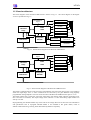
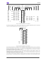
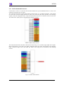
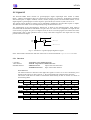
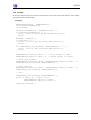
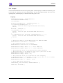
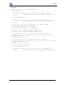
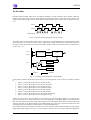
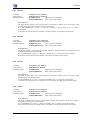
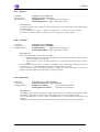
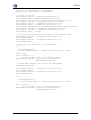
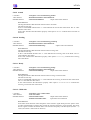
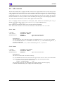
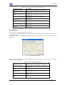
Fig. 4.1. RT-DAC/USB2 I/O CN1 connector
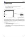
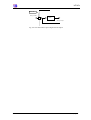
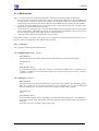
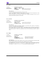
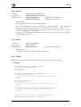
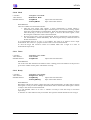
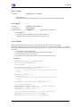
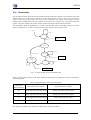
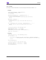
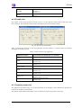
The analog and digital version of the RT-DAC/USB2 board is equipped additionally with the CN2 40-pin
connector. The pin assignment of the connector is shown in Fig. 4.2.
Analog output
Analog input
Ground
A/I 0
A/I 1
A/I 2
A/I 3
A/I 4
A/I 5
A/I 6
A/I 7
A/I 8
A/I 9
A/I 10
A/I 11
A/I 12
A/I 13
A/I 14
A/I 15
A/O 0
A/O 1
A/O 2
A/O 3
1
3
5
7
9
11
13
15
17
19
21
23
25
27
29
31
33
35
37
39
2
4
6
8
10
12
14
16
18
20
22
24
26
28
30
32
34
36
38
40
GND
GND
GND
GND
GND
GND
GND
GND
GND
GND
GND
GND
GND
GND
GND
GND
GND
GND
GND
GND
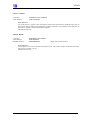
Fig. 4.2. RT-DAC/USB2 I/O CN2 connector
The RT-DAC/USB2 board is equipped with 16 multiplexed analog inputs located at the CN2 connector.
They are named from A/I 0 down to A/I 15. The output of the analog multiplexer is connected to the input of
the digital programmable analog amplifier. The board is also equipped with four 12-bit D/A converters.
These outputs are named from A/O 0 down to A/O 3.
Only 26 pins at the CN1 connector are used as general-purpose digital I/O signals (DIO0 to DIO25). The
remaining pins are the ground and power (GND, +5V, +3.3V). The general purpose digital I/O signals can be
individually configured to be either the input or output.
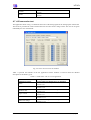
As the number of general-purpose digital I/O signals is limited, all of them are shared with the signals of the
specialized blocks. The specialized blocks are implemented as the modules in the on-board FPGA structure.
RT-DAC/USB2 - User’s Manual
page 11