1
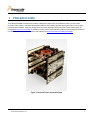
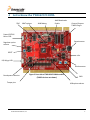
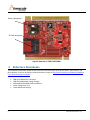
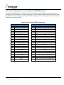
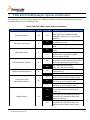
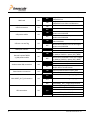
TWR-K21F120MA Tower Module User’s Manual Rev. 0 Freescale Semiconductor, Inc. Table of Contents 1 TWR-K21F120MA ..............................................................................................................................3 2 Contents ................................................................................................................................................4 3 TWR-K21F120MA Features.............................................................................................................4 4 Get to Know the TWR-K21F120MA ...............................................................................................5 5 Reference Documents .......................................................................................................................6 6 Hardware description.......................................................................................................................7 6.1 Block Diagram ............................................................................................................................................................................... 7 6.2 Microcontroller ............................................................................................................................................................................ 8 6.3 Clocking ......................................................................................................................................................................................... 10 6.4 System Power ............................................................................................................................................................................. 10 6.5 DryIce and RTC VBAT ............................................................................................................................................................ 10 6.6 Debug Interface ......................................................................................................................................................................... 10 6.7 OSJTAG ........................................................................................................................................................................................... 10 6.8 Cortex Debug Connector ....................................................................................................................................................... 11 6.9 Accelerometer ............................................................................................................................................................................ 12 6.10 Potentiometer, Pushbuttons, LEDs .............................................................................................................................. 12 6.11 General Purpose Tower Plug-in (TWRPI) Socket ................................................................................................. 13 6.12 USB ................................................................................................................................................................................................ 14 6.13 Secure Digital Card Slot ...................................................................................................................................................... 14 6.14 External Bus Interface - FlexBus ................................................................................................................................... 14 7 TWR-K21F120MA Jumper Options and Headers ................................................................... 15 8 Useful links ....................................................................................................................................... 17 TWR-K21F120MA Tower Module User’s Manual, Rev. 0, 09/2015 2 Freescale Semiconductor, Inc. 1 TWR-K21F120MA The TWR-K21F120MA microcontroller module is designed to work either in standalone mode or as part of the Freescale Tower System, a modular development platform that enables rapid prototyping and tool re-use through reconfigurable hardware. Take your design to the next level and begin constructing your Tower System today by visiting www.freescale.com/tower for additional Tower System microcontroller modules and compatible peripherals. For TWR-K21F120MA specific information and updates visit www.freescale.com/TWR-K21F120MA. Figure 1 Freescale Tower System Overview TWR-K21F120MA Tower Module User’s Manual, Rev. 0, 09/2015 Freescale Semiconductor, Inc. 3 2 Contents The TWR-K21F120MA contents include: TWR-K21F120MA board assembly 3 ft A to micro-B USB cable for debug interface and power or MK21FN1M0AVMC12 USB interface CR2025 coin cell battery for VBAT power supply Quick Start Guide TWR-K21F120MA Features 3 Tower-compatible microcontroller module MK21FN1M0AVMC12 MCU (120 MHz, 1 MB Flash, 128 KB RAM, low power, 121 MAPBGA package) Dual-role USB interface with Micro-AB USB connector General-purpose Tower Plug-in (TWRPI) socket On-board debug circuit: MC9S08JM60 open source JTAG (OSJTAG) with virtual serial port Three-axis accelerometer (MMA8451Q) Four (4) user-controllable LEDs Two (2) user pushbutton switches for GPIO interrupts One (1) user pushbutton switch for MCU reset Potentiometer Independent, battery-operated power supply for Real Time Clock (RTC) and tamper detection modules SD Card slot TWR-K21F120MA Tower Module User’s Manual, Rev. 0, 09/2015 4 Freescale Semiconductor, Inc. 4 Get to Know the TWR-K21F120MA JTAG VBAT options JM60 debug JM60 Bootloader Enable General Purpose TWRPI Plug-In Power/OSJTAG Micro-USB Potentiometer Regulator option selector RESET LEDs K21 Micro-USB microUSB Accelerometer Board power selection Figure 2 Front side of TWR-K21F120MA module (TWRPI devices not shown) Tamper pins SW2 SW3 USB option selector TWR-K21F120MA Tower Module User’s Manual, Rev. 0, 09/2015 Freescale Semiconductor, Inc. 5 Battery Receptacle SD Card Receptacle Figure 3 Back side of TWR-K21F120MA 5 Reference Documents The documents listed below should be referenced for more information on the Kinetis family, Tower System, and MCU Modules. These can be found in the documentation section of http://www.freescale.com/TWR-K21F120MA or http://www.freescale.com/kinetis TWR-K21F120MA-SCH: Schematics TWR-K21F120MA-PWA: Design Package K21P121M120SF5V2RM: Reference Manual Tower Configuration Tool Tower Mechanical Drawing TWR-K21F120MA Tower Module User’s Manual, Rev. 0, 09/2015 6 Freescale Semiconductor, Inc. 6 Hardware description The TWR-K21F120MA is a Tower MCU Module featuring the MK21FN1M0AVMC12 a Kinetis microcontroller in a 121 MAPBGA package with USB 2.0 full-speed on-the-go (OTG) controllers and system security and tamper detection with a secure real-time clock with independent battery supply. It is intended for use in the Freescale Tower System but can also operate stand-alone. An on-board OSJTAG debug circuit provides a JTAG interface and a power supply input through a single micro-USB connector. The block diagram of the TWR-K21F120MA board is presented in the following figure: 6.1 Block Diagram Tower Elevator Expansion Connectors 2 2 SDHC , I S, SPI, I C, ADC , USB , PWM, UARTs, FTM, FlexBus 5.0V 3.3V regulator 1.8V regulator 3.3V 1.8V 32.768 KHz XTAL 8 MHz XTAL 5.0V Micro USB Micro USB OSJTAG JTAG, Power , SCI JTAG K21F120MA 121 MABGA SCI Reset LED LED LED VBAT (RTC) SD Card Slot LED VDD USB (Device/Host) Battery Holder GPIO / Interrupts / LLWU DryIce Tamper SDHC 2 SPI, I C, ADC , GPIO DryIce Tamper Pins ADC C 2 I General Purpose Tower Plug-in (TWRPI) Freescale Device External Connectors Accelerometer MMA8451Q Interface Circuits Power Figure 4 Block Diagram of TWR-K21F120MA TWR-K21F120MA Tower Module User’s Manual, Rev. 0, 09/2015 Freescale Semiconductor, Inc. 7 6.2 Microcontroller The TWR-K21F120MA features the MK21FN1M0AVMC12 MCU. This 120 MHz microcontroller is part of the Kinetis K2x family and is implemented in a 121 MAPBGA package. The following table notes some of the features of the MK21FN1M0AVMC12 MCU. Table 1 Features of MK21FN1M0AVMC12 Feature Ultra low power Description – – – – Flash and SRAM – – – Mixed-signal capability – – – – – Performance – – – – – 11 low-power modes with power and clock gating for optimal peripheral activity and recovery times. Full memory and analog operation down to 1.71 V for extended battery life Low-leakage wake-up unit with up to six internal modules and sixteen pins as wake-up sources in low-leakage stop (LLS)/very low-leakage stop (VLLS) modes Low-power timer for continual system operation in reduced power states 1-MB flash featuring fast access times, high reliability, and four levels of security protection 128 KB of SRAM No user or system intervention to complete programming and erase functions and full operation down to 1.71 V Two high-speed 16-bit SAR ADCs with configurable resolution Single or differential output modes for improved noise rejection 500-ns conversion time achievable with programmable delay block triggering Three high-speed comparators providing fast and accurate motor overcurrent protection by driving PWMs to a safe state Optional analog voltage reference provides an accurate reference to analog blocks and replaces external voltage references to reduce system cost Two 12-bit DACs 120 MHz ARM Cortex-M4 core with DSP and FPU instruction set, single cycle MAC, and single instruction multiple data (SIMD) extensions Up to four channel DMA for peripheral and memory servicing with reduced CPU loading and faster system throughput Cross bar switch enables concurrent multi-master bus accesses, increasing bus bandwidth Independent flash banks allowing concurrent code execution and firmware updating with no performance degradation or complex coding routines TWR-K21F120MA Tower Module User’s Manual, Rev. 0, 09/2015 8 Freescale Semiconductor, Inc. Timing and Control – – – – Connectivity and Communications – – – – – – – – Reliability, Safety and Security – – – – – – – Three FlexTimers with a total of 12 channels Hardware dead-time insertion and quadrature decoding for motor control Carrier modulator timer for infrared waveform generation in remote control applications Four-channel 32-bit periodic interrupt timer provides time base for RTOS task scheduler or trigger source for ADC conversion and programmable delay block Full-Speed USB Device/Host/On-The-Go with device charge detect capability Optimized charging current/time for portable USB devices, enabling longer battery life USB low-voltage regulator supplies up to 120 mA off chip at 3.3 volts to power external components from 5-volt input Six UARTs: o one UART supports RS232 with flow control, RS485, ISO7816, IrDA o five UARTs support RS232 with flow control and RS485 One Inter-IC Sound (I2S) serial interface for audio system interfacing Two DSPI modules and two I2C modules Secured digital host controller (SDHC) A multi-function external bus interface called the FlexBus interface controller capable of interfacing to slave-only devices. Hardware Encryption co-processor for secure data transfer and storage. Faster than software implementations and with minimal CPU loading. Supports a wide variety of algorithms - DES, 3DES, AES, MD5, SHA-1, SHA-256 System security and tamper detection with secure real-time clock (RTC) and independent battery supply. Secure key storage with internal/external tamper detection for unsecured flash, temperature, clock, and supply voltage variations and physical attack detection Memory protection unit provides memory protection for all masters on the cross bar switch, increasing software reliability Cyclic redundancy check (CRC) engine validates memory contents and communication data, increasing system reliability Independently-clocked COP guards against clock skew or code runaway for fail-safe applications such as the IEC 60730 safety standard for household appliances External watchdog monitor drives output pin to safe state for external components in the event that a watchdog timeout occurs Included in Freescale’s product longevity program, with assured supply for a minimum of 10 years after launch TWR-K21F120MA Tower Module User’s Manual, Rev. 0, 09/2015 Freescale Semiconductor, Inc. 9 6.3 Clocking The Kinetis MCUs start up from an internal digitally controlled oscillator (DCO). Software can enable the main external oscillator (EXTAL0/XTAL0) if desired. The external oscillator/resonator can range from 32.768 KHz up to a 32 MHz. An 8 MHz crystal is the default external source for the MCG oscillator inputs (XTAL/EXTAL). A 32.768 KHz crystal is connected to the RTC oscillator inputs by default. By populating isolation resistors, other external clock sources for the MK21FN1M0AVMC12 include the CLKIN0 signal that can be provided through the TWR-ELEV or pin 20 of TWRPI connector J3. 6.4 System Power When installed into a Tower System, the TWR-K21F120MA can be powered from either an on-board source or from another source in the assembled Tower System. In stand-alone operation, the main power source (5.0 V) for the TWR-K21F120MA module is derived from either the OSJTAG USB mini-B connector (J2) or the MK21FN1M0AVMC12 USB micro-AB connector (J19). Two low-dropout regulators provide 3.3 V and 1.8 V supplies from the 5.0 V input voltage. Additionally, the 3.3 V regulator built into the MK21FN1M0AVMC12 MCU can be selected to power the 3.3 V bus. All the user selectable options can be configured using two headers, J11 and J17. Refer to sheet 5 of the TWR-K21F120MA schematics for more details. 6.5 DryIce and RTC VBAT The DryIce tamper detection module and the Real Time Clock (RTC) module on the MK21FN1M0AVMC12 have two modes of operation: system power-up and system power-down. During system power-down, the tamper detection module and the RTC are powered from the backup power supply (VBAT) and electrically isolated from the rest of the MCU. The TWR-K21F120MA provides a battery receptacle for a coin cell battery that can be used as the VBAT supply. The receptacle can accept common 20-mm diameter 3 V lithium coin cell batteries. 6.6 Debug Interface There are two debug interface options provided: the on-board OSJTAG circuit and an external ARM JTAG connector. The ARM-JTAG connector (J1) is a standard 2x10-pin connector providing an external debugger cable with access to the JTAG interface of the MK21FN1M0AVMC12. Alternatively, the on-board OSJTAG debug interface can be used to access the debug interface of the MK21FN1M0AVMC12. 6.7 OSJTAG An on-board MC9S08JM60 based Open Source JTAG (OSJTAG) circuit provides a JTAG debug interface to the MK21FN1M0AVMC12. A standard USB A male to micro-B male cable (provided) can be used for debugging via the USB connector (J2). The OSJTAG interface also provides a USB to serial bridge. Drivers for the OSJTAG interface are provided in the P&E Micro OSBDM/OSJTAG Tower Toolkit. These drivers and more utilities can be found online at http://www.pemicro.com/osbdm. TWR-K21F120MA Tower Module User’s Manual, Rev. 0, 09/2015 10 Freescale Semiconductor, Inc. 6.8 Cortex Debug Connector The Cortex Debug connector is a 20-pin (0.05") connector providing access to the SWD, JTAG, cJTAG, EzPort signals available on the K21 device. The pinout and K21 pin connections to the debug connector (J1) are shown in Table 2. Table 2 Cortex Debug connector Pin Function TWR-K21F120MA Connection 1 2 3 4 5 6 7 8 9 10 11 12 13 14 15 16 17 18 19 20 VTref TMS / SWDIO GND TCK / SWCLK GND TDO / SWO Key TDI GND Detect nRESET Target Power TRACECLK Target Power TRACEDATA[0] GND TRACEDATA[1] GND TRACEDATA[2] GND TRACEDATA[3] 3.3 V MCU supply (MCU_PWR) PTA3/SCI0_RTS_b/FTM0_CH0/JTAG_MS/SWD_DIO GND PTA0/SCI0_CTS_b/FTM0_CH5/JTAG_CLK/SWD_CLK/EZP_CLK GND PTA2/SCI0_TX/FTM0_CH7/JTAG_DO/TRACE_SWO/EZP_DO ― PTA1/SCI0_RX/FTM0_CH6/JTAG_DI/EZP_DI PTA4/FTM0_CH1/MS/NMI_b/EZP_CS_b RESET_b 5 V supply (via J6) PTE0/mADC0_SE10/SPI1_PCS1/UART1_TX/TRACE_CLKOUT/I2C1_SDA/RTC_CLKOUT 5 V supply (via J6) PTE4/LLWU_P2/SPI1_PCS0/UART3_TX/TRACE_D0 GND PTE3/ADC0_DM2/mADC0_DM1/SPI1_SIN/UART1_RTS/TRACE_D1/SPI1_SOUT GND PTE2/LLWU_P1/ADC0_DP2/mADC0_DP1/SPI1_SCK/UART1_CTS/TRACE_D2 GND PTE1/LLWU_P0/mADC0_SE11/SPI1_SOUT/UART1_RX/TRACE_D3/I2C1_SCL/SPI1_SIN TWR-K21F120MA Tower Module User’s Manual, Rev. 0, 09/2015 Freescale Semiconductor, Inc. 11 6.9 Accelerometer An MMA8451Q digital accelerometer is connected to the MK21FN1M0AVMC12 MCU through an I2C interface (I2C1) and GPIO/IRQ signals (PTB0 and PTB1). 6.10 Potentiometer, Pushbuttons, LEDs The TWR-K21F120MA also features: - a potentiometer connected to an ADC input signal (ADC0_SE12). two pushbutton switches (SW2 and SW3 connected to PTC7 and PTC6, respectively) four user-controllable LEDs connected to GPIO signals (optionally isolated using jumpers): o Green LED (D5) to PTD4 o Yellow LED (D6) to PTD5 o Orange LED (D8) to PTD6 o Blue LED (D9) to PTD7 TWR-K21F120MA Tower Module User’s Manual, Rev. 0, 09/2015 12 Freescale Semiconductor, Inc. 6.11 General Purpose Tower Plug-in (TWRPI) Socket The TWR-K21F120MA features a socket (J3 and J4) that can accept a variety of different Tower Plug-in modules featuring sensors, RF transceivers, and other peripherals. The General Purpose TWRPI socket provides access to I2C, SPI, IRQs, GPIOs, timers, analog conversion signals, TWRPI ID signals, reset, and voltage supplies. The pinout for the TWRPI Socket is defined in Table 3. Table 3 General Purpose TWRPI socket pinout Pin J4 Description Pin J3 Description 1 2 3 4 5 6 7 8 9 10 11 12 13 14 15 16 17 18 19 20 5 V VCC 3.3 V VCC GND 3.3 V VDDA VSS (Analog GND) VSS (Analog GND) VSS (Analog GND) ADC: Analog 0 ADC: Analog 1 VSS (Analog GND) VSS (Analog GND) ADC: Analog 2 VSS (Analog GND) VSS (Analog GND) GND GND ADC: TWRPI ID 0 ADC: TWRPI ID 1 GND Reset 1 2 3 4 5 6 7 8 9 10 11 12 13 14 15 16 17 18 19 20 GND GND I2C: SCL I2C: SDA GND GND GND GND SPI: MISO SPI: MOSI SPI: SS SPI: CLK GND GND GPIO: GPIO0/IRQ GPIO: GPIO1/IRQ UART: UART_RX or GPIO: GPIO2 UART: UART_TX or GPIO: GPIO3 UART: UART_CTS or GPIO: GPIO4/Timer UART: UART_RTS or GPIO: GPIO5/Timer TWR-K21F120MA Tower Module User’s Manual, Rev. 0, 09/2015 Freescale Semiconductor, Inc. 13 6.12 USB The MK21FN1M0AVMC12 features a full-speed/low-speed USB module with OTG/Host/Device capability and built-in transceiver. The TWR-K21F120MA routes the USB D+ and D- signals from the MCU via J24 jumper either to the onboard micro-AB USB connector (J19) or to the mini-AB USB connector (J14) on the TWR-SERIAL tower board. A power supply switch with an enable input signal and over-current flag output signal is used to supply power to the USB connector when the MK21FN1M0AVMC12 is operating in host mode. Port pin PTC8 is connected to the flag output signal and port pin PTC9 is used to drive the enable signal. Both PTC8 and PTC9 port pins can be isolated with jumpers (J23 and J22, respectively) if needed. 6.13 Secure Digital Card Slot A Secure Digital (SD) card slot is available on the TWR-K21F120MA connected to the SD Host Controller (SDHC) signals of the MCU. This slot will accept SD memory cards. Refer to the Table 4 “SD Card Socket Connection Table” for the SDHC signal connection details. Table 4 SD Card Socket Connection Pin Function TWR-K21F120MA Connection 1 2 3 4 5 6 7 SDHC0_D3 SDHC0_CMD VSS1 VDD SDHC0_DCL VSS2 SDHC0_D0 8 9 10 11 12 SDHC0_D1 SDHC0_D2 SD_CARD_DETECT CD_WP_COMMON SD_CARD_WP PTE4/LLWU_P2/SPI1_PCS0/UART3_TX/SDHC0_D3/TRACE_D0 PTE3/ADC0_DM2/ADC1_SE7A/SPI1_SIN/UART1_RTS/SDHC0_CMD/TRACE_D1/SPI1_SOUT GND 3.3 V board supply (V_BRD) PTE2/LLWU_P1/ADC0_DP2/ADC1_SE6A/SPI1_SCK/UART1_CTS/SDHC0_DCLK/TRACE_D2 GND PTE1/LLWU_P0/ADC1_SE5A/SPI1_SOUT/UART1_RX/SDHC0_D0/TRACE_D3/I2C1_SCL/SPI1_SI N PTE0/ADC1_SE4A/SPI1_PCS1/UART1_TX/SDHC0_D1/TRACE_CLKOUT/I2C1_SDA/RTC_CLKOUT PTE5/SPI1_PCS2/UART3_RX/SDHC0_D2/FTM3_CH0 PTC18/UART3_RTS/FB_TBST/FB_CS2/FB_BE15_8_BLS23_16 GND PTC19/UART3_CTS/FB_CS3/FB_BE7_0_BLS31_24/FB_TA 6.14 External Bus Interface - FlexBus The device features a multi-function external bus interface called the FlexBus interface controller capable of interfacing to slave-only devices. The FlexBus interface is not used directly on the TWR-K21F120MA. Instead, a subset of the FlexBus is connected to the Primary Connector so that the external bus can access devices on Tower peripheral modules. Refer to the sheet 8 of the TWR-K21F120MA schematic for more details. TWR-K21F120MA Tower Module User’s Manual, Rev. 0, 09/2015 14 Freescale Semiconductor, Inc. 7 TWR-K21F120MA Jumper Options and Headers The following is a list of all the jumper options on the TWR-K21F120MA. The default installed jumper settings are indicated by white text on a black background. Table 5 TWR-K21F120MA Jumper Options and Headers Option Jumper Tamper Connections JP1 Setting 2-3 1-2 MCU power connection J8 2-3 1-2 VBAT power source J7 2-3 ON JTAG board power selection J6 OFF OSJTAG bootloader selection J9 ON OFF 1-2 V_BRD power source (Board Power Selector) J17 3-5 5-7 1-2 VREG IN selector J11 5-6 6-8 Description JP1-1 through JP1-6 are connected to the MCU Tamper pins TAMPER0 through TAMPER5, respectively, for active tamper detection Connect on-board 3.3 V or 1.8 V supply (V_BRD) to MCU VDD Connect K21 USB regulator output to MCU VDD Connect VBAT to on-board 3.3 V or 1.8 V supply Connect VBAT to the higher voltage between MCU supply (MCU_PWR) or coin cell supply (VBATD) Connect OSJTAG 5V output (P5V_TRG_USB) to JTAG port (supports powering board from JTAG pod supporting 5V supply output) Disconnect OSJTAG 5V output (P5V_TRG_USB) from JTAG port OSJTAG bootloader mode (OSJTAG firmware reprogramming) Debugger mode Connect K21 USB regulator output (VOUT_3V3) to on-board supply (V_BRD) Connect 3.3 V on-board regulator output (P3V3) to on-board supply (V_BRD) Connect 1.8 V on-board regulator output (P1V8) to on-board supply (V_BRD) OSJTAG 5V output (P5V_TRG_USB) connected to on-board regulator input (VREG_IN) VBUS signal on micro-USB connector J19 connects to K21_VREGIN to allow standalone USB operation VBUS signal from Tower Elevator connector connects to K21_VREGIN to allow USB operation with complete Tower System TWR-K21F120MA Tower Module User’s Manual, Rev. 0, 09/2015 Freescale Semiconductor, Inc. 15 ON 10K pulldown resistor is disconnected from CD/DATA3 line 10K pulldown resistor is connected to CD/DATA3 line to allow card detection Connect PTD7 to USB ID pin OFF Disconnect PTD7 from USB ID pin OFF SDHC card J16 ON USB ID connection J21 ON USB power enable J22 OFF ON USB over-current flag J23 OFF USB option selector General Purpose TWRPI V_BRD power enable Accelerometer IRQ connection J24 1-2 2-3 ON J10 OFF J18 1-2 3-4 OFF Potentiometer connection J12 ON OFF 1-2 GPIO RESET_OUT_B Connection LED connections J13 J15 2-3 OFF 1-2 3-4 5-6 7-8 OFF Connect PTC9 to USB power enable on power switch MIC2026 Disconnect PTC9 from USB power enable on power switch MIC2026 Connect PTC8 to over-current flag on power switch MIC2026 Disconnect PTC8 from over-current flag on power switch MIC2026 USB micro J19 USB mini J14 on TWR-SER Connect on-board 1.8 V or 3.3 V supply (V_BRD) to TWRPI 3-V power (GPT_VBRD) Disconnect from-board 1.8 V or 3.3 V supply (V_BRD) to TWRPI 3-V power (GPT_VBRD) Connect PTB0 to INT1 pin of accelerometer Connect PTB1to INT2 pin of accelerometer Disconnect PTB0 and/or PTB1 from INT1 and/or INT2 of accelerometer Connect potentiometer to ADC0_SE12 Disconnect potentiometer from ADC0_SE12 Connect PTA14 to RESET_OUT_B signal Connect PTA17 to RESET_OUT_B signal Leave RESET_OUT_B signal disconnected Connect PTD4 to green LED (D5) Connect PTD5 to yellow LED (D6) Connect PTD6 to red LED (D8) Connect PTD7 to blue LED (D9) Disconnect PTD[4:7] from associated LED TWR-K21F120MA Tower Module User’s Manual, Rev. 0, 09/2015 16 Freescale Semiconductor, Inc. 8 Useful links ► www.freescale.com • www.freescale.com/kinetis • www.freescale.com/TWR-K21F120MA • http://www.freescale.com/kds ► www.iar.com/freescale ► www.mbed.com • http://www.mbed.org/handbook/Windows-serial-configuration ► www.segger.com • 9 http://www.segger.com/jlink-flash-download.html Revision History Revision 0 Date September, 2015 Description Initial release TWR-K21F120MA Tower Module User’s Manual, Rev. 0, 09/2015 Freescale Semiconductor, Inc. 17 How to Reach Us: Home Page: freescale.com Web Support: freescale.com/support Information in this document is provided solely to enable system and software implementers to use Freescale products. There are no express or implied copyright licenses granted hereunder to design or fabricate any integrated circuits based on the information in this document. Freescale reserves the right to make changes without further notice to any products herein. Freescale makes no warranty, representation, or guarantee regarding the suitability of its products for any particular purpose, nor does Freescale assume any liability arising out of the application or use of any product or circuit, and specifically disclaims any and all liability, including without limitation consequential or incidental damages. “Typical” parameters that may be provided in Freescale data sheets and/or specifications can and do vary in different applications, and actual performance may vary over time. All operating parameters, including “typicals,” must be validated for each customer application by customer's technical experts. Freescale does not convey any license under its patent rights nor the rights of others. Freescale sells products pursuant to standard terms and conditions of sale, which can be found at the following address: freescale.com/SalesTermsandConditions. Freescale, the Freescale logo, CodeWarrior, and Kinetis are trademarks of Freescale Semiconductor, Inc., Reg. U.S. Pat. & Tm. Off. Tower is a trademark of Freescale Semiconductor, Inc. All other product or service names are the property of their respective owners. © 2015 Freescale Semiconductor, Inc. All rights reserved. Document Number: TWR-K21F120MA Rev. 0 09/2015 TWR-K21F120MA Tower Module User’s Manual, Rev. 0, 09/2015 18 Freescale Semiconductor, Inc.