1
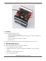
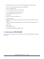
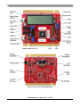
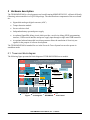
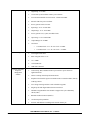
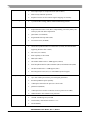
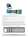
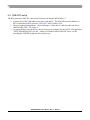
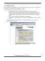
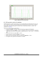
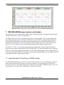
Freescale Semiconductor
Document Number: TWRKM34Z50UM
Rev. 1, 09/2013
User Manual
TWR-KM34Z50 Tower Module
User’s Manual
by: Michael Galda
Contents
1
TWR-KM34Z50M introduction................................................... 1
1 TWR-KM34Z50M introduction
2
Contents ....................................................................................... 2
3
TWR-KM34Z50M features ......................................................... 2
The TWR-KM34Z50M microcontroller module
is designed to work either in standalone mode or
as part of the Freescale Tower System, a
modular development platform that enables
rapid prototyping and tool reuse through
reconfigurable hardware. Take your design to
the next level and begin constructing your
Tower System today by visiting
www.freescale.com/Tower for additional Tower
System microcontroller modules and compatible
peripherals. For TWR-KM34Z50M specific
information and updates visit
www.freescale.com/TWR-KM34Z50M.
4
Get to know the TWR-KM34Z50M............................................. 3
5
Hardware description ................................................................... 5
5.1
Tower card block diagram................................................. 5
5.2
Kinetis M family microcontrollers .................................... 6
5.3
Clocking ............................................................................ 9
5.4
System power .................................................................... 9
5.5
iRTC tamper detection and RTC VBAT ......................... 10
5.6
Debug interface ............................................................... 10
5.7
OpenSDA ........................................................................ 10
5.8
Tilt sensor/accelerometer ................................................ 11
5.9
Potentiometer, temperature sensor, pushbuttons, LEDs .. 11
5.10
6
Figure 1 provides an overview of the Freescale
Tower system.
6.1
KM34Z50M CPU input current (Idd) measurement........ 12
6.2
K20 generator features .................................................... 12
6.3
K20 generator, USB-CDC, and FreeMaster GUI ............ 13
6.4
USB-CDC setup .............................................................. 14
6.5
FreeMaster setup ............................................................. 16
6.6
7
K20 generator control in FreeMaster............................... 17
TWR-KM34Z50M jumper options and headers......................... 18
7.1
8
General-purpose Tower Plug-in (TWRPI) socket ........... 18
Reference documents and useful links ....................................... 21
8.1
9
USB-to-serial interface .............................................. 11
Onboard K20 signal generator ................................................... 11
Useful links: .................................................................... 21
Revision history ......................................................................... 22
.
© 2013 Freescale Semiconductor, Inc.
_______________________________________________________________________
Figure 1. Freescale Tower System overview
2 Contents
The TWR-KM34Z50M contents include:
• TWR-KM34Z50M board assembly
• 3 feet A to mini-B USB cable for debug interface and power or USB-to-serial interface for
TWR-KM34Z50M
• CR2025 coin cell battery for VBAT power supply
• Quick Start Guide
For a summary of Freescale’s document types, see the Documentation page on freescale.com.
3 TWR-KM34Z50M features
The features of TWR-KM34Z50M tower system are listed below.
•
Tower-compatible microcontroller module
•
MKM34Z5128CLL5 MCU (50 MHz, 128 KB Flash, 16 KB RAM, low power, LQFP100
package)
•
USB interface with Mini-AB USB connector
•
Large 160-segment glass LCD
TWR-KM34Z50 Tower Module, Rev. 1, 09/2013
2
Freescale Semiconductor Inc.
•
Onboard debug circuit: open source JTAG/SWD (OpenSDA) with virtual serial port
•
Three-axis accelerometer/anti-tamper tilt sensor (MMA8491Q)
•
Four user-controllable LEDs
•
Two user pushbutton switches for GPIO interrupts
•
One user pushbutton switch for tamper detection
•
One user pushbutton switch for MCU reset
•
Potentiometer
•
Headers for direct GPIO and ADC access
•
External Tamper pins
•
Independent, battery-operated power supply for real-time clock (RTC) and tamper detection
modules
•
Onboard 7-channel sinusoidal signal generator with USB interface for emulating the AC net
waveforms
•
IRDA support
•
NTC temperature sensor
•
General-purpose Tower Plug-in (TWRPI) socket
4 Get to know the TWR-KM34Z50M
Figure 2 and Figure 3 present the front side and back side views of TWR-KM34Z50M tower module,
respectively.
TWR-KM34Z50 Tower Module, Rev. 1, 09/2013
Freescale Semiconductor Inc.
3
Figure 2. Front side of TWR-KM34Z50M module (TWRPI devices not shown)
Figure 3. Back side of TWR-KM34Z50M
TWR-KM34Z50 Tower Module, Rev. 1, 09/2013
4
Freescale Semiconductor Inc.
5 Hardware description
The TWR-KM34Z50M is a development tower board featuring MKM34Z128CLL5, a Kinetis-M family
(Metering) microcontroller in a LQFP-100 package. The other hardware components of the tower board
are:
•
Sigma-delta analog-to-digital converter (ADC)
•
Tamper detection module
•
Secure real-time clock
•
Independent battery-operated power supply
•
An onboard OpenSDA debug circuit which provides a serial wire debug (SWD) programming
interface, USB-to-serial interface and power supply input through a single mini-USB connector.
•
An optional onboard sinusoidal waveform generator allows the emulation of electricity net
signals for the purpose of software development.
The TWR-KM34Z50M is intended for use in the Freescale Tower System but can also operate in
standalone mode.
5.1 Tower card block diagram
The following figure presents the block diagram of TWR-KM34Z50M tower module.
Tower Elevator Expansion Connectors
SD_ADC, SAR_ADC, VREF, QTM /PWM, SPI, I2C, SCI
5.0V
3.3V
regulator
32.768 KHz XTAL
8 MHz XTAL
5.0V
K20 OpenSDA
SWD, Power, SCI
USB
Micro
LED
LED
3ph signal gen.
K20 50MHz
QFN-32
U
I
VDD
6x PWM
LP filters
5.0V
VBAT (RTC)
KM34 50MHz
LQFP-100
(socket-IC footprint)
Freescale Device
LED
LED
LLWU /AWIC
LED
LED
SAR_ADC
I2C
SPI, I C, ADC, GPIO
General Purpose
Tower Plug-in
(TWRPI)
GPIO / Interrupts
Σ∆ADC 4x
2
General Purpose
Tower Plug-in
(TWRPI-Sensor)
Infrared Port
SCI
RESET
Battery
Holder
10-pin JTAG / SWD
IR Output
Comparator
SWD
SAR_ADC
USB
Mini-B
3.3V
LCD
Tilt sensor
MMA8491Q
External Connectors
Interface Circuits
Power
Figure 4. Block diagram of TWR-KM34Z50M tower board
TWR-KM34Z50 Tower Module, Rev. 1, 09/2013
Freescale Semiconductor Inc.
5
5.2 Kinetis M family microcontrollers
The devices in Kinetis M (KM) family are 32-bit MCUs in 90 nm Thin Film Storage (TFS) embedded
flash technology. These devices are primarily focused to serve the metering markets for smart single
phase energy meters in India, China, and the European Union countries and two-phase meters in the
U.S. and Japan.
KM family targets EN 50470-1, EN 50470-3, IEC 62053-21, IEC 62053-22, and IEC 62053-23 class of
meters.
KM devices are based on 32-bit ARM® Cortex®-M0+ core with integrated analog front end (AFE). CPU
clock rates on these devices can reach up to 50 MHz. The KM family of devices includes highly
accurate sigma delta (SD) ADC, programmable gain amplifier (PGA), high precision internal voltage
reference, flash memory, RAM, phase compensation logic block, and other peripherals. KM family
provides tamper detection and accurate real-time clock on all devices.
The significant features of MKM34Z128CLL5 MCU are listed in the following table.
Table 1. Features of MKM34Z128CLL5
Feature
Operating
characteristics
Core
Clocks
Description
•
Voltage range 2.7–3.6 V (with AFE)
•
Voltage range 1.71–3.6 V (without AFE)
•
Flash programming voltage from 1.71–3.6 V
•
iRTC battery supply range 1.71–3.6 V
•
Temperature range (TA) –40 °C to 85 °C
•
Flexible modes of operation
•
High-performance ARM Cortex-M0+ Core
•
Upto 50 MHz of core clock frequency
•
Supports v6-M Instruction Set Architecture (ISA) including all 16-bit v7-M
instructions plus a number of 32-bit Thumb-2 instructions
•
100% compatible with Cortex-M0
•
0.95 DMIPS per MHz performance when executing from internal RAM
•
Nested Vectored Interrupt Controller
•
32 vectored interrupts
•
Four programmable priority levels
•
MHz Oscillator
•
Mid Range: 1–8 MHz
TWR-KM34Z50 Tower Module, Rev. 1, 09/2013
6
Freescale Semiconductor Inc.
Analog
System, protection,
and power
management
features
•
High Range: 8–32 MHz
•
32.768 kHz crystal oscillator in iRTC power domain
•
Two internal trimmable clock references: 32 kHz and 4 MHz
•
Internal 1 kHz low-power oscillator
•
PLL to generate clocks for AFE
•
Input range: 31.25–39.0625 kHz
•
Output range: 11.72–14.65 MHz
•
FLL to generate core, system, and flash clocks
•
Input range: 31.25–39.0625 kHz
•
Output Range: 20–50 MHz
•
Clock ratio
o
Core:Bus:Flash = 2:1:1 for core clock > 25 MHz
o
Core:Bus:Flash = 1:1:1 for core clock <= 25 MHz
•
24-bit Sigma Delta ADC
•
PGA with gains from 1 to 32
•
1.2 V VREF
•
16-bit SAR ADC
•
CMP with 6-bit DAC
•
Various Stop, Wait, and Run modes to provide lower power based on
application needs
•
AWIC to wakeup from Stop and VLPS modes
•
Peripheral clock enable register can disable clocks to unused modules, thereby
reducing currents
•
Low-voltage warning and detect with selectable trip points
•
Illegal opcode and illegal address detection with reset
•
Hardware Programmable CRC module to support fast cyclic redundancy
checks (CRC)
•
Random Number Generator (RNGA)
•
128-bit unique chip identifier
•
Software and hardware watchdog with external monitor pin
TWR-KM34Z50 Tower Module, Rev. 1, 09/2013
Freescale Semiconductor Inc.
7
Debug
Timers
Communications
Input/Output
Memory
•
Four tamper inputs for Tamper Detection (Part of iRTC)
•
Flash security and block protection
•
Peripheral crossbar to allow internal signal remapping for flexibility
•
2-pin Serial Wire Debug (SWD): Standard ARM debug interface
•
Independent Real-Time Clock (iRTC) independently powered by battery and
on-chip crystal clock drift compensation
•
Quad Timer (four channels)
•
Programmable Interrupt Timer (PIT)
•
Low-Power Timer (LPTMR)
•
Universal Asynchronous Receiver/Transmitter (UART) (all UART modules
supporting hardware flow control)
•
ISO 7816 (on 2 UARTs)
•
IrDA capability on all UARTs
•
DMA (all UARTs)
•
One UART module with 5 V AMR support (UART1)
•
Serial Peripheral Interface (SPI) with FIFO (SPI1) and without FIFO (SPI0)
•
One SPI module with 5 V AMR support (SPI1)
•
Inter-Integrated Circuit (I2C) (x2) with SMBUS protocol support
•
Up to nine eGPIO ports and one port with digital glitch filters
•
Pin interrupt/DMA request capability
•
eGPIO pins connected to the processor’s local 32-bit
•
platform bus (RGPIO)
•
eGPIO pins also accessible via IPS bus accesses (protected via AIPS)
•
eGPIO module to have inbuilt access protection
•
128 KB / 64 KB single array FLASH
•
Flash memory read and write down to 1.71 V
•
No FlexMemory
TWR-KM34Z50 Tower Module, Rev. 1, 09/2013
8
Freescale Semiconductor Inc.
Display
Power consumption
•
Core:Flash frequency is 2:1
•
1:1 for low core frequency (<= 25 MHz)
•
16 KB of single access RAM
•
4x40 Segment LCD
•
8x36 Segment LCD
•
3 V LCD glass supported with segment fault detection
•
RUN Mode (all modules OFF): 6.0 mA
IDD Equation: 1.14 mA + 97 μA/MHz
Note: For more details, see the Power modes section of MKM34Z128CLL5RM:
Reference Manual, available on freescale.com.
5.3 Clocking
The Kinetis-M starts up from an internal reference clock = 2 MHz core and 1 MHz bus clock. When the
MCU boots in LPBOOT (Low-Power Boot) mode, the core and system clocks are divided by 8.
CPU software can enable RTC oscillator connected to EXTAL0/XTAL0 if desired, or the second highfrequency oscillator connected to EXTAL1/XTAL1 can be used.
RTC crystal oscillator range is: 31.25 kHz to 39.0625 kHz (typically 32.768 kHz)
High-frequency crystal oscillator range: 1 kHz to 32 MHz.
Optionally, two (fast = 4 MHz and slow = 32.768 kHz) internal clock references (IRC) can be used.
The CPU frequency can be increased by using the FLL (DCO) or PLL clock features. In most of the
applications, usage of the single 32 kHz external crystal is considered. PLL with a fixed multiplier
(x375) can be used for clocking the AFE running at ~12.2 MHz and the FLL can be used for clocking of
the CPU core (up to 50 MHz) and the rest of the MCU modules.
Note: For the best AFE results, usage of the precise external clock is recommended.
5.4 System power
When installed into a Tower System, the TWR-KM34Z50M can be powered from either an onboard
source or from another source in the assembled Tower System.
In standalone operation, the main power source (5.0 V) for the TWR-KM34Z50M module is derived
from the OpenSDA USB mini-B connector (J14). A low-dropout regulator provides 3.3 V supply
voltage from the 5.0 V input voltage. All the user-selectable options can be configured using the
jumpers: J1, J6, J7, J19, and S1. See pages 3, 5 and 6 of the TWR-KM34Z50M schematics, available on
freescale.com for more details.
TWR-KM34Z50 Tower Module, Rev. 1, 09/2013
Freescale Semiconductor Inc.
9
5.5 iRTC tamper detection and RTC VBAT
The tamper detection module and the Real-Time Clock (RTC) module on the MKM34Z128CLL5 have
two modes of operation: system power-up and system power-down. During system power-down, the
tamper detection module and the RTC are powered from the backup power supply (VBAT) and
electrically isolated from the rest of the MCU. The TWR-KM34Z50M provides a battery receptacle for
a coin cell battery that can be used as the VBAT supply. The receptacle can accept common 20-mm
diameter 3 V lithium coin cell batteries.
5.6 Debug interface
There are two debug interface options provided: the onboard OpenSDA circuit and an external ARM
JTAG/SWD connector. The ARM-JTAG/SWD connector (J3 SWD) is a standard 2x5-pin connector
providing an external debugger cable with access to the JTAG interface of the MKM34Z128CLL5.
Alternatively, the onboard OSJTAG debug interface can be used to access the debug interface of the
MKM34Z128CLL5.
•
J13 (K20_SWD) connector is used by factory for flashing the OpenSDA firmware to K20
device.
•
J15 (GEN_SWD) connector is used for auxiliary K20-based on-board generator.
5.7 OpenSDA
An onboard MK20DX128VMF5-based OpenSDA circuit provides a SWD debug interface to the
MKM34Z128CLL5. A standard USB A male to mini-B male cable (provided) can be used for
debugging via the USB connector (J14). The OpenSDA interface also provides a USB-to-serial bridge.
Drivers for the OpenSDA interface are provided in the P&E Micro OSBDM/OSJTAG Tower Toolkit.
These drivers and more utilities can be found online at www.pemicro.com/OpenSDA.
Cortex Debug connector
The Cortex Debug connector is a 10-pin (0.05") connector providing access to the SWD signals
available on the KM34 device. The pinout and KM34 pin connections to the debug connector (J3) are
shown in the following table.
Table 2. Cortex Debug connector
Pin
1
2
3
4
5
Function
V_BRD
SWD_DIO_TGTMCU
GND
SWD_CLK_TGTMCU
GND
TWR-KM34Z50M connection
3.3 V MCU supply (MCU_PWR)
PTE6/CMP0P2/PXBAR_IN5/SCI2_RXD/LLWU_P5/SWD_IO
GND
PTE7/AD6/PXBAR_OUT5/SCI2_TXD/SWD_CLK
GND
TWR-KM34Z50 Tower Module, Rev. 1, 09/2013
10
Freescale Semiconductor Inc.
6
7
8
9
10
―
―
―
―
PTE1/RESET
NC
NC
NC
NC
RST_TGTMCU_B
5.8 Tilt sensor/accelerometer
MMA8491Q digital accelerometer is connected to the MKM34Z128CLL5 MCU through an I2C
interface (I2C0) and tamper signals (TAMPER0, 1, 2).
5.9 Potentiometer, temperature sensor, pushbuttons, LEDs
The TWR-KM34Z50M also has the following features.
• A potentiometer connected to an ADC input signal (PTG1/AD10)
• Temperature sensor (NTC) connected to an ADC input signal (PTF0/AD7)
• Battery voltage measurement connected to ADC input (PTF2/AD9)
• Two pushbutton switches (SW1 and SW2 connected to PTD0 and PTE4, respectively)
• IRDA interface through PTC2, PTC3
• Four user-controllable LEDs connected to GPIO signals (optionally isolated using switch S1):
o Green LED (D3) to PTE5
o Red LED (D4) to PTF1
o Orange LED (D5) to PTD1/GPIO3
o Yellow LED (D6) to PTC1/GPIO4/CMP1P1
5.10 USB-to-serial interface
The onboard K20 OpenSDA circuit supports the USB-to-serial port emulation through the USB CDC
Serial Class device.
This means whenever the Tower card is connected to the computer USB port, the board is recognized as
a new virtual COM port (COM5 or COM6 in the most of the cases). The user can connect with the
embedded application running on KM34 device and see the output on the PC running the serial terminal
application.
6 Onboard K20 signal generator
The K20 signal generator is capable of generating seven sinusoidal waveforms for emulating the real
electricity net (3-phase current + 3-phase voltage) with configurable frequency, amplitude, phase shift,
and harmonic distortion. The maximum amplitude of the generated waveforms is 1.0 V (pk-to-pk), so
they can be measured by ADC working in Single-Ended mode. The generator can be interfaced via the
TWR-KM34Z50 Tower Module, Rev. 1, 09/2013
Freescale Semiconductor Inc.
11
dedicated USB connector to PC running the FreeMaster GUI application, where the net parameters can
be easily tuned.
The external analog signals can be connected directly to the ADC inputs by header J17.
6.1 KM34Z50M CPU input current (Idd) measurement
The K20 is able to measure KM34 Idd current and send the value over the USB connection to the PC
running the FreeMaster application.
One of the K20 ADC channels is dedicated for KM34 Idd current consumption measurement. The input
current is scanned as the voltage drop on the 10 Ω shunt resistor connected in the MCU Vdd supply rail.
This voltage drop is amplified and converted by differential U/I amplifier (U18) and then converted to
appropriate voltage range for K20 ADC input. With these specific component values, the user can
measure Idd currents in the range 0.5–20 mA, with the reasonable precision. With the larger current
sensing shunt resistor values, better precision can be obtained for the lower currents.
NOTE: The onboard generator firmware was under development by the date of releasing of this
document, so this feature is not supported on the first tower cards. The users will be able to download
the K20 generator firmware later from the Freescale web site, freescale.com. The firmware will be
programmed in the factory on the new revision of the tower cards.
6.2 K20 generator features
Following is a list of the features of K20 sinusoidal signal generator. See Figure 5.
• Based on K20 (QFN32) subfamily of Kinetis MCUs
• Seven PWM signals, capable to generate sinusoidal waveforms (3xI + 3xU, that is, 3-phase
current + 3-phase voltage)
• Configurable amplitude, frequency, and phase shift
• Jumper connections to ADC inputs
• Virtual serial port (USB-CDC) for PC running the FreeMaster application
• KM34 input Idd current measurement through the dedicated K20 ADC channel
TWR-KM34Z50 Tower Module, Rev. 1, 09/2013
12
Freescale Semiconductor Inc.
FreeMaster
USB
USB
(CDC)
6x PWM
LP filters
LED
LED
3ph signal gen.
K20 50MHz
QFN-32
3xi
Σ∆
4xch
3xu
SAR
3xch
KM34
Figure 5. K20 signal generator concept
6.3 K20 generator, USB-CDC, and FreeMaster GUI
To use the onboard K20 generator, the K20 USB and generator output must be enabled by the onboard
DIP switch, SW5.
The SW5 default setting is read by program after the power-on reset, so the tower card power cycling is
required to apply the changes.
The USB and the generator can be disabled by SW5 to reduce the potential noise caused by K20
circuits.
This is important in the cases, when the generator feature is not needed and the noise may affect the
ADC performance. If the K20 USB communication is disabled, the MCU goes to the Very Low-Power
Stop (VLPS) mode immediately after tower card power-on reset. When only the KM34 MCU Idd
current sensing functionality is needed, the generator output can be disabled to reduce the noise coming
from PWM, while the Idd current measurement via USB is still active. Alternatively, the current sensing
shunt resistor can be shorted (bypassed) by the jumper J19 to avoid the voltage drop on the resistor. See
the table given below.
Table 3. K20 generator default operation (SW5 settings)
Option
DIP SW5
settings
Position
Setting
Description
1
OFF
2
OFF
K20 USB communication disabled, K20 in Very Low-Power
Stop (VLPS) mode
Generator output disabled
1
ON
2
ON
USB communication and KM34 current sensing enabled,
green LED ON
Generator output enabled, amber LED ON
TWR-KM34Z50 Tower Module, Rev. 1, 09/2013
Freescale Semiconductor Inc.
13
6.4 USB-CDC setup
The K20 generator USB-CDC connectivity has been tested under MS-Windows 7.
1. Connect both of the USB cables to the tower card and PC. The K20 USB must be enabled via
SW5 as described in K20 generator, USB-CDC, and FreeMaster GUI.
2. Choose Computer Management > Device Manager > Other device, and select the new device
"KM34Z50M_GEN". See Figure 6.
3. To update the driver for the device, choose "Browse my computer for driver SW", find and select
“TWR_KM34Z50M_K20_Gen.inf”, which is a Windows-based USB-CDC driver .inf file
including the VID/PID assigned to Freescale devices.
TWR-KM34Z50 Tower Module, Rev. 1, 09/2013
14
Freescale Semiconductor Inc.
Figure 6. USB-CDC driver setup in Windows device manager
TWR-KM34Z50 Tower Module, Rev. 1, 09/2013
Freescale Semiconductor Inc.
15
6.5 FreeMaster setup
Run the FreeMaster GUI application as soon as you see the new Virtual Com Port device available and
driver properly installed in the device manager. See Figure 7.
In the FreeMaster application, follow the steps given below:
1. Click the STOP button from the Menu (the communication should be stopped).
2. Click the Project tab and the Options window appears. In the Options window, select
RS232, 9600 baud, and appropriate COMx from the listbox, and click OK. See Figure 7.
If the appropriate COM port is not available, disconnect and connect the USB cable
again.
3. Now, click the STOP button to establish the communication.
4. If you get the error message, power cycle the tower card and check the proper COM port
again.
If everything is OK, you can see the Idd current chart and generated signal waveforms (if
enabled) as shown in Figure 8.
Figure 7. FreeMaster communication setup
TWR-KM34Z50 Tower Module, Rev. 1, 09/2013
16
Freescale Semiconductor Inc.
Figure 8. KM34 Idd current measurement
6.6 K20 generator control in FreeMaster
The K20 generator is capable of generating up to seven independent sinusoidal signals. The user can
easily control the parameters of the generated signals through the global variables in the FreeMaster
watch window. The generated signal waveforms can be recorded by FreeMaster “recorder” and
visualized. See Figure 9.
The user can control following signal features:
• Frequency (FreqHz = 50–60 Hz, step 0.1 Hz) time base common for all channels
• Magnitude of the signal (magn = 0–100%) = magnitude of the basic zero harmonic component
of the signal while sum all of the harmonic components must be ≤ 100% , that is, ~1.0V peak-topeak
• Phase shift of the basic signal (shift = 0–360°)
• Higher harmonic components: harm3, 5, 7 (0–100%)
• Phase shifts for the individual harmonic components (harmXsh = 0–360°)
• The signals can be generated as sinusoidal or “rectified”.
TWR-KM34Z50 Tower Module, Rev. 1, 09/2013
Freescale Semiconductor Inc.
17
Figure 9. Example of generated harmonic signals in FreeMaster Recorder window
7 TWR-KM34Z50M jumper options and headers
The following is a list of all the jumper options on the TWR-KM34Z50M. The default installed jumper
settings are indicated in Table 5 by the bold text.
The GPIO Header J10 (Table 6) contains tamper pins, two analog inputs, CLK out check signal, and
most of the peripheral interface BUS pins like SPI, I2C, and SCI. AFE external modulator signals are
also available on this header, so that the customized board with the external AFE modulator can be
interfaced. Most of the pins can be used normally as GPIO. Tamper pins can be connected to the Tilt
sensor (U7) X,Y,Z outputs, or to the external tamper button (SW3) using the jumper shunts.
The header J17 (Table 7) is the Analog inputs/generator output header which contains the auxiliary
signal generator outputs, analog inputs of SD, and SAR ADCs. The generator signals can be connected
directly to ADC inputs using the jumper shunts. Or the external analog signals can be connected directly
to the ADC inputs. If the SD-ADC is used for measurement in Single-Ended mode, the ADMx wires can
be grounded to VSSA using the jumper shunts.
7.1 General-purpose Tower Plug-in (TWRPI) socket
The TWR-KM34Z50M features a socket (J11 and J12) that can accept a variety of different Tower Plug-in
modules featuring sensors, RF transceivers, and other peripherals. The general-purpose TWRPI socket
provides access to I2C, SPI, IRQs, GPIOs, timers, analog conversion signals, TWRPI ID signals, reset, and
voltage supplies. The pinout for the TWRPI socket is defined in this table.
TWR-KM34Z50 Tower Module, Rev. 1, 09/2013
18
Freescale Semiconductor Inc.
Table 4. General-purpose TWRPI socket pinout
J12
J11
Pin
Description
Pin
Description
1
2
3
4
5
6
7
8
9
10
11
12
13
14
15
16
17
18
5 V VCC
3.3 V VCC
GND
3.3 V VDDA
VSS (Analog GND)
VSS (Analog GND)
VSS (Analog GND)
ADC: Analog 0
ADC: Analog 1
VSS (Analog GND)
VSS (Analog GND)
ADC: Analog 2
VSS (Analog GND)
VSS (Analog GND)
GND
GND
ADC: TWRPI ID 0
ADC: TWRPI ID 1
1
2
3
4
5
6
7
8
9
10
11
12
13
14
15
16
17
18
19
GND
19
20
Reset
20
GND
GND
I2C: SCL
I2C: SDA
GND
GND
GND
GND
SPI: MISO
SPI: MOSI
SPI: SS
SPI: CLK
GND
GND
GPIO: GPIO0/IRQ
GPIO: GPIO1/IRQ
UART: UART_RX or GPIO: GPIO2
UART: UART_TX or GPIO: GPIO3
UART: UART_CTS or GPIO:
GPIO4/Timer
UART: UART_RTS or GPIO:
GPIO5/Timer
Table 5. Jumpers and switch options
Option
Jumper
Setting
Description
Connect VBAT to on-board 3.3 V supply
MCU power
connection
J1
1-2
2-3
VREF out
selection
MCU_PWR
selection
J2
Connect VBAT to the higher voltage between MCU supply
(MCU_PWR) or VBATD
ON
VREF connected to ELEVATOR edge
OFF
VREF available on pins
ON
MCU powered from V_BRD 3.3V on board regulator
OFF
MCU can be supplied by external voltage connected to pin 1 of the
jumper J6.
J6
TWR-KM34Z50 Tower Module, Rev. 1, 09/2013
Freescale Semiconductor Inc.
19
Analog power
enable
Potentiometer
enable
(might be
hardwired)
Temperature
sensor enable
(might be
hardwired)
Low-power
current
measurement
OpenSDA Reset
enabled
DIP Switch S1
connections
ON
Connect analog voltages to MCU_PWR
OFF
Connect analog voltages to MCU_PWR, external VDDA can be
applied
Connect PTG1/AD10 to potentiometer R20
J7
ON
Disconnect PTG1/AD10 from potentiometer R20
J8
OFF
ON
Connect PTF0/AD7 to temperature sensor
Disconnect PTF0/AD7 to temperature sensor
J9
OFF
ON
J19
OFF
Low-power current measurement bypassed
Low-power current measurement enabled
ON
KM34 Reset input driven by K20 OpenSDA
OFF
KM34 Reset input isolated from OpenSDA
ON
Connect PTE5 to GREEN LED (D3)
ON
Connect PTF1 to RED LED (D4)
ON
Connect PTD1 to ORANGE LED (D5)
ON
Connect PTC1 to YELLOW LED (D6)
ON
Connect IRDA Tx LED (D7) to PTC2
ON
Connect IRDA Rx Transistor (Q1) to PTC3
ON
Connect Serial EEPROM data to I2C0 data
ON
Connect Serial EEPROM clock to I2C0 clock
ON
Connect TILT_ENABLE (MMA8491Q) signal to PTF7
ON
Connect VBAT voltage measurement signal to PTF2/AD9
J20
S1
Table 6. GPIO header (J10) signal connections
MCU signal
J10 PIN
SW3 (Tamper switch)
SW3 (Tamper switch)
TILT_XOUT
TILT_YOUT
TILT_ZOUT
V_BRD
PTI1/SCI1_TXD
PTE0/I2C0_SDA
PTF6/SPI1_MOSI
1
2
3
5
4
6
7
9
8
10
11
13
12
14
15
17
16
18
MCU signal
SW3 to TAMPER1 (when closed)
SW3 to TAMPER2 (when closed)
TILT_XOUT to TAMPER0
TILT_YOUT to TAMPER1
TILT_ZOUT to TAMPER2
PTI0/SCI1_RXD
GND
PTD7/I2C0_SCL
PTF5/SPI1_MISO
TWR-KM34Z50 Tower Module, Rev. 1, 09/2013
20
Freescale Semiconductor Inc.
PTF4/SPI1_SCK
PTA6/AFE_EXT_MOD_IN1
PTC0/AFE_EXT_MOD_IN2
PTB7/AFE_EXT_CLK_IN
PTA7/AFE_EXT_CLK_OUT
19
21
23
25
27
20
22
24
26
28
PTF3/SPI1_SS
PTF7/CLKOUT
PTG0
PTC5/AD0
PTC6/AD1
VSSA_SAR
29
30
GND
Table 7. Analog Inputs / Generator output (J17)
MCU signal
GEN_OUT0
GEN_OUT1
GEN_OUT2
GEN_OUT3
GEN_OUT4
GEN_OUT5
GEN_OUT6
VSSA
VSSA
VSSA
VSSA
J17 PIN
MCU signal
1
3
5
7
9
11
13
2
4
6
8
10
12
14
15
16
17
19
18
20
EXT_SAR_AD2
EXT_SD_ADM0 (can short to
VSSA)
EXT_SD_ADM1
EXT_SD_ADM2
21
22
EXT_SD_ADM3
EXT_SD_ADP0
EXT_SD_ADP1
EXT_SD_ADP2
EXT_SD_ADP3
EXT_SAR_AD0
EXT_SAR_AD1
8 Reference documents and useful links
The documents and links listed below should be referenced for more information on the Kinetis family,
Tower System, and MCU Modules. The documents can be found in the documentation section of
www.freescale.com/TWR-KM34Z50M or www.freescale.com/kinetis.
• TWR-KM34Z50M-SCH: Schematics
• TWR-KM34Z50M-PWA: Design Package
• MKM34Z128CLL5RM: Reference Manual
• Tower Configuration Tool
• Tower Mechanical Drawing
Note: Some documents may be temporarily unavailable at the time of releasing of this user
guide.
8.1 Useful links:
•
freescale.com
TWR-KM34Z50 Tower Module, Rev. 1, 09/2013
Freescale Semiconductor Inc.
21
•
www.freescale.com/twr-km34z50M
•
www.iar.com/freescale
•
pemicro.com
•
www.pemicro.com/OpenSDA
•
OSBDM/OSJTAG Virtual Serial Toolkit
•
www.freescale.com/FreeMaster
9 Revision history
The following table presents the revision history of the document.
Revision
Date
Topic
Change description
0
04/2013
—
Initial release
1
09/2013
Get to know the
TWR-KM34Z50M
Updated Figure 2
USB-CDC setup
Changed list item [2] to Choose
Computer Management > Device
Manager>Other device, and select
the new device
"KM34Z50M_GEN"
Updated Figure 6
Changed “fsl_ucwxp.inf” to
“TWR_KM34Z50M_K20_Gen.inf”
in list item [3]
General-purpose
Tower Plug-in
(TWRPI) socket
Updated Table 5
Throughout the
document
Minor editorial changes
TWR-KM34Z50 Tower Module, Rev. 1, 09/2013
22
Freescale Semiconductor Inc.
How to Reach Us:
Home Page:
freescale.com
Web Support:
freescale.com/support
Information in this document is provided solely to enable system and software
implementers to use Freescale products. There are no express or implied copyright
licenses granted hereunder to design or fabricate any integrated circuits based on the
information in this document.
Freescale reserves the right to make changes without further notice to any products
herein. Freescale makes no warranty, representation, or guarantee regarding the
suitability of its products for any particular purpose, nor does Freescale assume any
liability arising out of the application or use of any product or circuit, and specifically
disclaims any and all liability, including without limitation consequential or incidental
damages. “Typical” parameters that may be provided in Freescale data sheets and/or
specifications can and do vary in different applications, and actual performance may vary
over time. All operating parameters, including “typicals,” must be validated for each
customer application by customer’s technical experts. Freescale does not convey any
license under its patent rights nor the rights of others. Freescale sells products pursuant
to standard terms and conditions of sale, which can be found at the following address:
freescale.com/SalesTermsandConditions.
Freescale, the Freescale logo, and Kinetis are trademarks of Freescale Semiconductor,
Inc. All other product or service names are the property of their respective owners. Tower
is a trademark of Freescale Semiconductor, Inc. ARM is the registered trademark of ARM
Limited.
© 2013 Freescale Semiconductor, Inc. All rights reserved.
Document Number: TWRKM34Z50UM
Revision 1, September 2013
Mouser Electronics
Authorized Distributor
Click to View Pricing, Inventory, Delivery & Lifecycle Information:
Freescale Semiconductor:
MKM34Z128CLL5