1
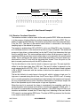
The data in the transmit serial shifter is prefixed by a start bit (logic zero) and suffixed
by the ninth data bit, if M = 1, and by one stop bit. The ninth data bit can be used as
normal data or as an extra stop bit. A parity bit is substituted if PE = 1. This data stream
is shifted out over the TXD pin. When the data is completely shifted out and no preamble or send break is requested, then TC is set to one and the TXD pin remains high
(logic one or mark).
Parity generation is enabled by setting PE in SCCR1 to a one. The last data bit, bit
eight (or bit nine of the data if M = 1), is used as the parity bit, which is inserted between
the normal data bits and the stop bit(s).
When TE is cleared, the transmitter yields control of the TXD pin in the following manner. If no information is being shifted out (i.e., if the transmitter is in an idle state, TC =
1), then the TXD pin reverts to being a general-purpose I/O pin. If a transmission is still
in progress (TC = 0), the characters in the transmit serial shifter continue to be shifted
out normally, followed by any queued break. When finished, TXD reverts to being a
general-purpose I/O pin. To avoid terminating the transmitter before all data is transferred, the software should always wait for TDRE to be set before clearing TE.
Transmissions may be purposely aborted by the send break function. By writing SBK
in SCCR1 to a one, a nonzero integer multiple of ten bit-times (eleven if 9-bit data format is specified) of space (logic zero) is transmitted. If SBK is set while a transmission
is in progress, the character in the transmit serial shifter finishes normally (including
the stop bit) before the break function begins. Break frames are sent until either SBK
or TE is cleared. To guarantee the minimum break time, SBK should be quickly toggled to one and then back to zero. After the break time, at least one bit-time of mark
idle (logic one) is transmitted to ensure that a subsequent start bit can be recognized.
The TXD pin has several control options to provide flexible operation. WOMS in
SCCR1 can select either open-drain output (for wired-OR operation) or normal CMOS
output. WOMS controls the function of the TXD pin whether the pin is being used for
SCI transmissions (TE = 1) or as a general-purpose I/O pin.
In an SCI system with multiple transmitters, the wired-OR mode should be selected for
the TXD pin of all transmitters, allowing multiple output pins to be coupled together. In
the wired-OR mode, an external pull-up resistor on the TXD pin is necessary.
In some systems, a mark (logic one) signal is desired on the TXD pin, even when the
transmitter is disabled. This is accomplished by writing a one to PORTQS in the appropriate position and configuring the TXD pin as an output in DDRQS. When the
transmitter releases control of the TXD pin, it reverts to driving a logic one output,
which is the same as mark or idle.
5.4 Receiver Operation
The receiver can be divided into two segments. The first is the receiver bit processor
logic that synchronizes to the asynchronous receive data and evaluates the logic
sense of each bit in the serial stream. The second receiver segment controls the functional operation and the interface to the CPU including the conversion of the serial data
stream to parallel access by the CPU.
QSM
REFERENCE MANUAL
SCI SUBMODULE
MOTOROLA
5-15