1
SAFETY PRECAUTIONS
(Read these precautions before using this product.)
Before using this product, please read this manual and the relevant manuals carefully and pay full attention
to safety to handle the product correctly.
The precautions given in this manual are concerned with this product only. For the safety precautions of the
programmable controller system, refer to the user's manual for the CPU module used.
In this manual, the safety precautions are classified into two levels: "
WARNING" and "
CAUTION".
WARNING
Indicates that incorrect handling may cause hazardous conditions,
resulting in death or severe injury.
CAUTION
Indicates that incorrect handling may cause hazardous conditions,
resulting in minor or moderate injury or property damage.
Under some circumstances, failure to observe the precautions given under "
CAUTION" may lead to
serious consequences.
Observe the precautions of both levels because they are important for personal and system safety.
Make sure that the end users read this manual and then keep the manual in a safe place for future
reference.
1
[Design Precautions]
WARNING
● Configure safety circuits external to the programmable controller to ensure that the entire system
operates safely even when a fault occurs in the external power supply or the programmable controller.
Failure to do so may result in an accident due to an incorrect output or malfunction.
(1) Emergency stop circuits, protection circuits, and protective interlock circuits for conflicting
operations (such as forward/reverse rotations or upper/lower limit positioning) must be configured
external to the programmable controller.
(2) When the programmable controller detects an abnormal condition, it stops the operation and all
outputs are:
• Turned off if the overcurrent or overvoltage protection of the power supply module is activated.
• Held or turned off according to the parameter setting if the self-diagnostic function of the CPU
module detects an error such as a watchdog timer error.
Also, all outputs may be turned on if an error occurs in a part, such as an I/O control part, where
the CPU module cannot detect any error. To ensure safety operation in such a case, provide a
safety mechanism or a fail-safe circuit external to the programmable controller. For a fail-safe
circuit example, refer to the "GENERAL SAFETY REQUIREMENTS" chapter in the Safety
Guidelines included with the CPU module or head module.
(3) Outputs may remain on or off due to a failure of a component such as a transistor in an output
circuit. Configure an external circuit for monitoring output signals that could cause a serious
accident.
● In an output circuit, when a load current exceeding the rated current or an overcurrent caused by a
load short-circuit flows for a long time, it may cause smoke and fire. To prevent this, configure an
external safety circuit, such as a fuse.
● Configure a circuit so that the programmable controller is turned on first and then the external power
supply. If the external power supply is turned on first, an accident may occur due to an incorrect output
or malfunction.
● For the operating status of each station after a communication failure, refer to relevant manuals for
each network. Failure to do so may result in an accident due to an incorrect output or malfunction.
● When changing data from a peripheral device connected to the CPU module to the running
programmable controller, configure an interlock circuit in the program to ensure that the entire system
will always operate safely. For other forms of control (such as program modification or operating
status change) of a running programmable controller, read the relevant manuals carefully and ensure
that the operation is safe before proceeding. Especially, when a remote programmable controller is
controlled by an external device, immediate action cannot be taken if a problem occurs in the
programmable controller due to a communication failure. To prevent this, configure an interlock circuit
in the program, and determine corrective actions to be taken between the external device and CPU
module in case of a communication failure.
2
[Design Precautions]
CAUTION
● Do not install the control lines or communication cables together with the main circuit lines or power
cables. Keep a distance of 100mm or more between them. Failure to do so may result in malfunction
due to noise.
● During control of an inductive load such as a lamp, heater, or solenoid valve, a large current
(approximately ten times greater than normal) may flow when the output is turned from off to on.
Therefore, use a module that has a sufficient current rating.
● After the CPU module is powered on or is reset, the time taken to enter the RUN status varies
depending on the system configuration, parameter settings, and/or program size. Design circuits so
that the entire system will always operate safely, regardless of the time.
[Installation Precautions]
WARNING
● Shut off the external power supply (all phases) used in the system before mounting or removing a
module. Failure to do so may result in electric shock or cause the module to fail or malfunction.
[Installation Precautions]
CAUTION
● Use the programmable controller in an environment that meets the general specifications in the Safety
Guidelines provided with the CPU module or head module. Failure to do so may result in electric
shock, fire, malfunction, or damage to or deterioration of the product.
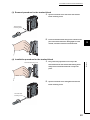
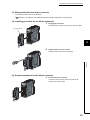
● To interconnect modules, engage the respective connectors and securely lock the module joint levers
until they click. Incorrect interconnection may cause malfunction, failure, or drop of the module.
● Do not directly touch any conductive parts and electronic components of the module. Doing so can
cause malfunction or failure of the module.
[Wiring Precautions]
WARNING
● Shut off the external power supply (all phases) used in the system before wiring. Failure to do so may
result in electric shock or cause the module to fail or malfunction.
● After installation and wiring, attach the included terminal cover to the module before turning it on for
operation. Failure to do so may result in electric shock.
3
[Wiring Precautions]
CAUTION
● Individually ground the FG and LG terminals of the programmable controller with a ground resistance
of 100 ohms or less. Failure to do so may result in electric shock or malfunction.
● Use applicable solderless terminals and tighten them within the specified torque range.
If any spade solderless terminal is used, it may be disconnected when a terminal block screw comes
loose, resulting in failure.
● Check the rated voltage and terminal layout before wiring to the module, and connect the cables
correctly.
Connecting a power supply with a different voltage rating or incorrect wiring may cause a fire or
failure.
● Connectors for external devices must be crimped or pressed with the tool specified by the
manufacturer, or must be correctly soldered. Incomplete connections may cause short circuit, fire, or
malfunction.
● Securely connect the connector to the module.
● Do not install the control lines or communication cables together with the main circuit lines or power
cables. Keep a distance of 100mm or more between them. Failure to do so may result in malfunction
due to noise.
● Tighten the terminal block screws within the specified torque range. Undertightening can cause short
circuit, fire, or malfunction. Overtightening can damage the screw and/or module, resulting in drop,
short circuit, fire, or malfunction.
● When disconnecting the cable from the module, do not pull the cable by the cable part. For the cable
with connector, hold the connector part of the cable.
For the cable connected to the terminal block, loosen the terminal screw.
Pulling the cable connected to the module may result in malfunction or damage to the module or
cable.
● Prevent foreign matter such as dust or wire chips from entering the module. Such foreign matter can
cause a fire, failure, or malfunction.
● A protective film is attached to the top of the module to prevent foreign matter, such as wire chips,
from entering the module during wiring. Do not remove the film during wiring. Remove it for heat
dissipation before system operation.
● Mitsubishi programmable controllers must be installed in control panels. Connect the main power
supply to the power supply module in the control panel through a relay terminal block.
Wiring and replacement of a power supply module must be performed by qualified maintenance
personnel with knowledge of protection against electric shock.
For wiring methods, refer to the MELSEC-L CPU Module User's Manual (Hardware Design,
Maintenance and Inspection).
4
[Startup and Maintenance Precautions]
WARNING
● Do not touch any terminal while power is on. Doing so will cause electric shock or malfunction.
● Correctly connect the battery connector. Do not charge, disassemble, heat, short-circuit, solder, or
throw the battery into the fire. Also, do not expose it to liquid or strong shock.
Doing so will cause the battery to produce heat, explode, ignite, or leak, resulting in injury and fire.
● Shut off the external power supply (all phases) used in the system before cleaning the module or
retightening the terminal block screws or connector screws. Failure to do so may result in electric
shock.
[Startup and Maintenance Precautions]
CAUTION
● Before performing online operations (especially, program modification, forced output, and operating
status change) for the running CPU module from the peripheral device connected, read relevant
manuals carefully and ensure the safety. Improper operation may damage machines or cause
accidents.
● Do not disassemble or modify the module. Doing so may cause failure, malfunction, injury, or a fire.
● Use any radio communication device such as a cellular phone or PHS (Personal Handy-phone
System) more than 25cm away in all directions from the programmable controller. Failure to do so
may cause malfunction.
● Shut off the external power supply (all phases) used in the system before mounting or removing a
module. Failure to do so may cause the module to fail or malfunction.
● Tighten the terminal block screws or connector screws within the specified torque range.
Undertightening can cause drop of the component or wire, short circuit, or malfunction. Overtightening
can damage the screw and/or module, resulting in drop, short circuit, or malfunction.
● After the first use of the product (module, display unit, and terminal block), do not connect/disconnect
the product more than 50 times (in accordance with IEC 61131-2). Exceeding the limit may cause
malfunction.
● Before handling the module, touch a conducting object such as a grounded metal to discharge the
static electricity from the human body. Failure to do so may cause the module to fail or malfunction.
[Disposal Precautions]
CAUTION
● When disposing of this product, treat it as industrial waste.
5
CONDITIONS OF USE FOR THE PRODUCT
(1) Mitsubishi programmable controller ("the PRODUCT") shall be used in conditions;
i) where any problem, fault or failure occurring in the PRODUCT, if any, shall not lead to any major
or serious accident; and
ii) where the backup and fail-safe function are systematically or automatically provided outside of
the PRODUCT for the case of any problem, fault or failure occurring in the PRODUCT.
(2) The PRODUCT has been designed and manufactured for the purpose of being used in general
industries.
MITSUBISHI SHALL HAVE NO RESPONSIBILITY OR LIABILITY (INCLUDING, BUT NOT
LIMITED TO ANY AND ALL RESPONSIBILITY OR LIABILITY BASED ON CONTRACT,
WARRANTY, TORT, PRODUCT LIABILITY) FOR ANY INJURY OR DEATH TO PERSONS OR
LOSS OR DAMAGE TO PROPERTY CAUSED BY the PRODUCT THAT ARE OPERATED OR
USED IN APPLICATION NOT INTENDED OR EXCLUDED BY INSTRUCTIONS, PRECAUTIONS,
OR WARNING CONTAINED IN MITSUBISHI'S USER, INSTRUCTION AND/OR SAFETY
MANUALS, TECHNICAL BULLETINS AND GUIDELINES FOR the PRODUCT.
("Prohibited Application")
Prohibited Applications include, but not limited to, the use of the PRODUCT in;
• Nuclear Power Plants and any other power plants operated by Power companies, and/or any
other cases in which the public could be affected if any problem or fault occurs in the PRODUCT.
• Railway companies or Public service purposes, and/or any other cases in which establishment of
a special quality assurance system is required by the Purchaser or End User.
• Aircraft or Aerospace, Medical applications, Train equipment, transport equipment such as
Elevator and Escalator, Incineration and Fuel devices, Vehicles, Manned transportation,
Equipment for Recreation and Amusement, and Safety devices, handling of Nuclear or
Hazardous Materials or Chemicals, Mining and Drilling, and/or other applications where there is a
significant risk of injury to the public or property.
Notwithstanding the above, restrictions Mitsubishi may in its sole discretion, authorize use of the
PRODUCT in one or more of the Prohibited Applications, provided that the usage of the PRODUCT
is limited only for the specific applications agreed to by Mitsubishi and provided further that no
special quality assurance or fail-safe, redundant or other safety features which exceed the general
specifications of the PRODUCTs are required. For details, please contact the Mitsubishi
representative in your region.
6
INTRODUCTION
Thank you for purchasing the Mitsubishi MELSEC-L series programmable controllers.
This manual describes safety precautions, specifications, and functions.
Before using this product, please read this manual and the relevant manuals carefully and develop familiarity with the
functions and performance of the MELSEC-L series programmable controller to handle the product correctly.
Remark
Operating procedures are explained using GX Works2.
When using GX Developer, refer to the following.
Page 90, Appendix 4
7
COMPLIANCE WITH EMC AND LOW VOLTAGE
DIRECTIVES
(1) Method of ensuring compliance
To ensure that Mitsubishi programmable controllers maintain EMC and Low Voltage Directives when incorporated
into other machinery or equipment, certain measures may be necessary. Please refer to one of the following
manuals.
• MELSEC-L CPU Module User's Manual (Hardware Design, Maintenance and Inspection)
• MELSEC-L CC-Link IE Field Network Head Module User's Manual
• Safety Guidelines (This manual is included with the CPU module or head module.)
The CE mark on the side of the programmable controller indicates compliance with EMC and Low Voltage
Directives.
(2) Additional measures
No additional measures are necessary for the compliance of this product with EMC and Low Voltage Directives.
8
RELEVANT MANUALS
(1) CPU module user's manual
Manual name
manual number (model code)
Description
MELSEC-L CPU Module User's Manual (Hardware Design, Maintenance and
Inspection)
SH-080890ENG, 13JZ36
Specifications of the CPU modules, power supply modules, display unit,
branch module, extension module, SD memory cards, and batteries,
information on how to establish a system, maintenance and inspection, and
troubleshooting
(2) Head module User's Manual
Manual name
manual number (model code)
Description
MELSEC-L CC-Link IE Field Network Head Module User's Manual
SH-080919ENG, 13JZ48
Specifications, procedures before operation, system configuration, installation,
wiring, settings, and troubleshooting of the head module
MELSEC-L SSCNET III/H Head Module User's Manual
SH-081152ENG, 13JZ78
Specifications, procedures before operation, system configuration, installation,
wiring, settings, and troubleshooting of the head module
(3) Operating manual
Manual name
manual number (model code)
Description
GX Works2 Version 1 Operating Manual (Common)
SH-080779ENG, 13JU63
GX Developer Version 8 Operating Manual
SH-080373E, 13JU41
System configuration, parameter settings, and online operations of GX
Works2, which are common to Simple projects and Structured projects
Operating methods of GX Developer, such as programming, printing,
monitoring, and debugging
(4) User's manual for optional items
Manual name
manual number (model code)
Relay Terminal Module User's Manual (Hardware) A6TE2-16SRN
IB-66833, 13JL53
Description
Specifications and part names of the A6TE2-16SRN
9
CONTENTS
CONTENTS
SAFETY PRECAUTIONS . . . . . . . . . . . . . . . . . . . . . . . . . . . . . . . . . . . . . . . . . . . . . . . . . . . . . . . . . . . . . 1
CONDITIONS OF USE FOR THE PRODUCT . . . . . . . . . . . . . . . . . . . . . . . . . . . . . . . . . . . . . . . . . . . . . 6
INTRODUCTION . . . . . . . . . . . . . . . . . . . . . . . . . . . . . . . . . . . . . . . . . . . . . . . . . . . . . . . . . . . . . . . . . . . . 7
COMPLIANCE WITH EMC AND LOW VOLTAGE DIRECTIVES . . . . . . . . . . . . . . . . . . . . . . . . . . . . . . . 8
RELEVANT MANUALS . . . . . . . . . . . . . . . . . . . . . . . . . . . . . . . . . . . . . . . . . . . . . . . . . . . . . . . . . . . . . . . 9
MANUAL PAGE ORGANIZATION . . . . . . . . . . . . . . . . . . . . . . . . . . . . . . . . . . . . . . . . . . . . . . . . . . . . . . 12
TERMS . . . . . . . . . . . . . . . . . . . . . . . . . . . . . . . . . . . . . . . . . . . . . . . . . . . . . . . . . . . . . . . . . . . . . . . . . . 14
PACKING LIST . . . . . . . . . . . . . . . . . . . . . . . . . . . . . . . . . . . . . . . . . . . . . . . . . . . . . . . . . . . . . . . . . . . . 14
CHAPTER 1 PRODUCT LINEUP
15
1.1
Product Lineup . . . . . . . . . . . . . . . . . . . . . . . . . . . . . . . . . . . . . . . . . . . . . . . . . . . . . . . . . . . . . 15
1.2
How to Read the Model Name . . . . . . . . . . . . . . . . . . . . . . . . . . . . . . . . . . . . . . . . . . . . . . . . . 16
CHAPTER 2 PART NAMES
18
CHAPTER 3 BEFORE USING I/O MODULE
20
3.1
Input Module . . . . . . . . . . . . . . . . . . . . . . . . . . . . . . . . . . . . . . . . . . . . . . . . . . . . . . . . . . . . . . . 20
3.2
Output Module . . . . . . . . . . . . . . . . . . . . . . . . . . . . . . . . . . . . . . . . . . . . . . . . . . . . . . . . . . . . . 21
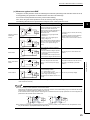
3.3
I/O Combined Module. . . . . . . . . . . . . . . . . . . . . . . . . . . . . . . . . . . . . . . . . . . . . . . . . . . . . . . . 27
CHAPTER 4 SPECIFICATIONS
4.1
4.2
4.3
28
General Specifications . . . . . . . . . . . . . . . . . . . . . . . . . . . . . . . . . . . . . . . . . . . . . . . . . . . . . . . 28
Input Module Specifications . . . . . . . . . . . . . . . . . . . . . . . . . . . . . . . . . . . . . . . . . . . . . . . . . . . 29
4.2.1
LX10 AC input module . . . . . . . . . . . . . . . . . . . . . . . . . . . . . . . . . . . . . . . . . . . . . . . . . . . . . . .29
4.2.2
LX28 AC input module . . . . . . . . . . . . . . . . . . . . . . . . . . . . . . . . . . . . . . . . . . . . . . . . . . . . . . .31
4.2.3
LX40C6 DC input module . . . . . . . . . . . . . . . . . . . . . . . . . . . . . . . . . . . . . . . . . . . . . . . . . . . .32
4.2.4
LX41C4 DC input module . . . . . . . . . . . . . . . . . . . . . . . . . . . . . . . . . . . . . . . . . . . . . . . . . . . .34
4.2.5
LX42C4 DC input module . . . . . . . . . . . . . . . . . . . . . . . . . . . . . . . . . . . . . . . . . . . . . . . . . . . .36
Output Module Specifications . . . . . . . . . . . . . . . . . . . . . . . . . . . . . . . . . . . . . . . . . . . . . . . . . . 38
4.3.1
LY10R2 contact output module . . . . . . . . . . . . . . . . . . . . . . . . . . . . . . . . . . . . . . . . . . . . . . . .39
4.3.2
LY18R2A contact output module (All points independent) . . . . . . . . . . . . . . . . . . . . . . . . . . . .40
4.3.3
LY20S6 triac output module . . . . . . . . . . . . . . . . . . . . . . . . . . . . . . . . . . . . . . . . . . . . . . . . . . .41
4.3.4
LY28S1A triac output module (All points independent) . . . . . . . . . . . . . . . . . . . . . . . . . . . . . .42
4.3.5
LY40NT5P transistor output module (Sink type) . . . . . . . . . . . . . . . . . . . . . . . . . . . . . . . . . . .44
4.3.6
LY41NT1P transistor output module (Sink type) . . . . . . . . . . . . . . . . . . . . . . . . . . . . . . . . . . .45
4.3.7
LY42NT1P transistor output module (Sink type) . . . . . . . . . . . . . . . . . . . . . . . . . . . . . . . . . . .47
4.3.8
LY40PT5P transistor output module (Source type) . . . . . . . . . . . . . . . . . . . . . . . . . . . . . . . . .49
4.3.9
LY41PT1P transistor output module (Source type) . . . . . . . . . . . . . . . . . . . . . . . . . . . . . . . . .50
4.3.10 LY42PT1P transistor output module (Source type) . . . . . . . . . . . . . . . . . . . . . . . . . . . . . . . . .52
4.4
I/O Combined Module Specifications . . . . . . . . . . . . . . . . . . . . . . . . . . . . . . . . . . . . . . . . . . . . 53
4.4.1
LH42C4NT1P DC input/transistor output combined module (Sink type) . . . . . . . . . . . . . . . . .54
4.4.2
LH42C4PT1P DC input/transistor output combined module (Source type) . . . . . . . . . . . . . . .56
CHAPTER 5 SYSTEM CONFIGURATION
10
58
CHAPTER 6 INSTALLATION AND WIRING
61
6.1
Installation Environment and Installation Position . . . . . . . . . . . . . . . . . . . . . . . . . . . . . . . . . . 61
6.2
Wiring . . . . . . . . . . . . . . . . . . . . . . . . . . . . . . . . . . . . . . . . . . . . . . . . . . . . . . . . . . . . . . . . . . . . 62
6.3
6.2.1
For the 18-point screw terminal block module . . . . . . . . . . . . . . . . . . . . . . . . . . . . . . . . . . . . .62
6.2.2
For the 40-pin connector type module . . . . . . . . . . . . . . . . . . . . . . . . . . . . . . . . . . . . . . . . . . .64
Input Wiring Examples . . . . . . . . . . . . . . . . . . . . . . . . . . . . . . . . . . . . . . . . . . . . . . . . . . . . . . . 66
CHAPTER 7 VARIOUS SETTINGS
68
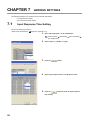
7.1
Input Response Time Setting . . . . . . . . . . . . . . . . . . . . . . . . . . . . . . . . . . . . . . . . . . . . . . . . . . 68
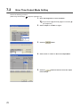
7.2
Error Time Output Mode Setting . . . . . . . . . . . . . . . . . . . . . . . . . . . . . . . . . . . . . . . . . . . . . . . . 70
CHAPTER 8 TROUBLESHOOTING
71
8.1
Troubleshooting for Input Circuit. . . . . . . . . . . . . . . . . . . . . . . . . . . . . . . . . . . . . . . . . . . . . . . . 71
8.2
Troubleshooting for Output Circuit . . . . . . . . . . . . . . . . . . . . . . . . . . . . . . . . . . . . . . . . . . . . . . 75
APPENDICES
81
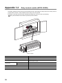
Appendix 1 Optional Items . . . . . . . . . . . . . . . . . . . . . . . . . . . . . . . . . . . . . . . . . . . . . . . . . . . . . . . . . 81
Appendix 1.1
Connector/terminal block converter modules. . . . . . . . . . . . . . . . . . . . . . . . . . . . . . . .81
Appendix 1.2
Relay terminal module (A6TE2-16SRN) . . . . . . . . . . . . . . . . . . . . . . . . . . . . . . . . . . .86
Appendix 1.3
Dedicated cables with connector . . . . . . . . . . . . . . . . . . . . . . . . . . . . . . . . . . . . . . . . .87
Appendix 1.4
Converter modules and interface modules (FA goods) . . . . . . . . . . . . . . . . . . . . . . . .87
Appendix 2 Checking Serial Number . . . . . . . . . . . . . . . . . . . . . . . . . . . . . . . . . . . . . . . . . . . . . . . . . 88
Appendix 3 Compatibility of L series and Q series I/O module . . . . . . . . . . . . . . . . . . . . . . . . . . . . . 89
Appendix 4 When Using GX Developer . . . . . . . . . . . . . . . . . . . . . . . . . . . . . . . . . . . . . . . . . . . . . . . 90
Appendix 5 External Dimensions . . . . . . . . . . . . . . . . . . . . . . . . . . . . . . . . . . . . . . . . . . . . . . . . . . . . 91
Appendix 5.1
I/O modules . . . . . . . . . . . . . . . . . . . . . . . . . . . . . . . . . . . . . . . . . . . . . . . . . . . . . . . . .91
Appendix 5.2
Connectors. . . . . . . . . . . . . . . . . . . . . . . . . . . . . . . . . . . . . . . . . . . . . . . . . . . . . . . . . .93
Appendix 5.3
Connector/terminal block converter modules. . . . . . . . . . . . . . . . . . . . . . . . . . . . . . . .94
Appendix 5.4
Cable for connector/terminal block converter module . . . . . . . . . . . . . . . . . . . . . . . . .95
REVISIONS . . . . . . . . . . . . . . . . . . . . . . . . . . . . . . . . . . . . . . . . . . . . . . . . . . . . . . . . . . . . . . . . . . . . . . . 96
WARRANTY . . . . . . . . . . . . . . . . . . . . . . . . . . . . . . . . . . . . . . . . . . . . . . . . . . . . . . . . . . . . . . . . . . . . . . 97
TRADEMARKS . . . . . . . . . . . . . . . . . . . . . . . . . . . . . . . . . . . . . . . . . . . . . . . . . . . . . . . . . . . . . . . . . . . . 98
11
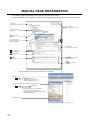
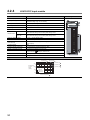
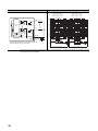
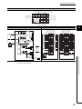
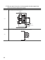
MANUAL PAGE ORGANIZATION
In this manual, pages are organized and the symbols are used as shown below.
The following illustration is for explanation purpose only, and should not be referred to as an actual documentation.
"" is used for
screen names and items.
The chapter of
the current page is shown.
shows operating
procedures.
shows mouse
operations.*1
[ ] is used for items
in the menu bar and
the project window.
The section of
the current page is shown.
Ex. shows setting or
operating examples.
shows reference
manuals.
shows notes that
requires attention.
shows
reference pages.
shows useful
information.
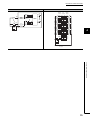
*1
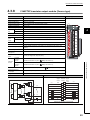
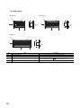
The mouse operation example is provided below. (For GX Works2)
Menu bar
Ex.
[Online]
[Write to PLC...]
Select [Online] on the menu bar,
and then select [Write to PLC...].
A window selected in the view selection area is displayed.
Ex.
[Parameter]
Project window
[PLC Parameter]
Select [Project] from the view selection
area to open the Project window.
In the Project window, expand [Parameter] and
select [PLC Parameter].
View selection area
12
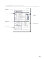
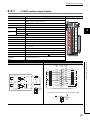
Pages describing specifications are organized as shown below.
The following illustration is for explanation purpose only, and should not be referred to as an actual documentation.
Model name and
module name
Module specifications
Appearance
Derating chart
(only for input modules)
Terminal connections
External connections
13
TERMS
Unless otherwise specified, this manual uses the following terms.
Term
Description
CPU module
Abbreviation for the MELSEC-L series CPU module
Power supply module
Abbreviation for the MELSEC-L series power supply module
Display unit
A liquid crystal display to be attached to the CPU module
LCPU
Another term for the MELSEC-L series CPU module
GX Works2
The product name of the software package for the MELSEC programmable controllers
GX Developer
L series I/O module
Abbreviation for the MELSEC-L series I/O module
Q series I/O module
Abbreviation for the MELSEC-Q series I/O module
I/O module
Another term for the MELSEC-L series I/O module
ACTB
Abbreviation for the AC05TB, AC10TB, AC20TB, AC30TB, AC50TB, AC80TB, and AC100TB
ACTE
Abbreviation for the AC06TE, AC10TE, AC30TE, AC50TE, and AC100TE
PACKING LIST
The following items are included in the package of this product. Before use, check that all the items are included.
I/O module
Module
14
Before Using the Product
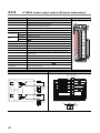
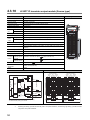
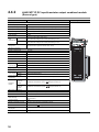
CHAPTER 1 PRODUCT LINEUP
CHAPTER 1
1.1
PRODUCT LINEUP
1
Product Lineup
(1) Input module
Module name
AC Input module
DC Input module
Number of occupied
I/O points
Input specifications
Current
consumption
Weight
Model name
Reference
Terminal block
100 to 120VAC, 16 points
16 points
90mA
0.17kg
LX10
Page 29,
Section 4.2.1
Terminal block
100 to 240VAC, 8 points
16 points
80mA
0.15kg
LX28
Page 31,
Section 4.2.2
Terminal block
24VDC, 16 points
16 points
90mA
0.15kg
LX40C6
Page 32,
Section 4.2.3
40-pin connector
24VDC, 32 points
32 points
100mA
0.11kg
LX41C4
Page 34,
Section 4.2.4
40-pin connector (× 2)
24VDC, 64 points
64 points
120mA
0.12kg
LX42C4
Page 36,
Section 4.2.5
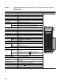
(2) Output module
Module name
Contact output module
Sink type
Transistor
output
module
Source
type
Current
consumption
Weight
Model name
Reference
Terminal block
240VAC/24VDC, 2A/1 point, 16 points
16 points
460mA
0.21kg
LY10R2
Page 39,
Section 4.3.1
Terminal block
240VAC/24VDC, 2A/1 point, 8 points
All points independent
16 points
260mA
0.14kg
LY18R2A
Page 40,
Section 4.3.2
Terminal block
100 to 240VAC, 0.6A/1 point, 16 points
16 points
300mA
0.22kg
LY20S6
Page 41,
Section 4.3.3
Terminal block
100 to 240VAC, 1A/1 point, 8 points
All points independent
16 points
200mA
0.15kg
LY28S1A
Page 42,
Section 4.3.4
Terminal block
12 to 24VDC, 0.5A/1 point, 16 points
16 points
100mA
0.15kg
LY40NT5P
Page 44,
Section 4.3.5
40-pin connector
12 to 24VDC, 0.1A/1 point, 32 points
32 points
140mA
0.11kg
LY41NT1P
Page 45,
Section 4.3.6
40-pin connector (× 2)
12 to 24VDC, 0.1A/1 point, 64 points
64 points
190mA
0.12kg
LY42NT1P
Page 47,
Section 4.3.7
Terminal block
12 to 24VDC, 0.5A/1 point, 16 points
16 points
100mA
0.15kg
LY40PT5P
Page 49,
Section 4.3.8
40-pin connector
12 to 24VDC, 0.1A/1 point, 32 points
32 points
140mA
0.11kg
LY41PT1P
Page 50,
Section 4.3.9
40-pin connector (× 2)
12 to 24VDC, 0.1A/1 point, 64 points
64 points
190mA
0.12kg
LY42PT1P
Page 52,
Section 4.3.10
(3) I/O combined module
Module name
DC
input/transistor
output
combined
module
Input
specifications
Sink type
Source type
40-pin connector
24VDC, 32 points
Output
specifications
40-pin connector
12 to 24VDC,
0.1A/1 point, 32
points
Number of
occupied
I/O points
Current
consumption
Weight
Model name
Reference
32 points
160mA
0.12kg
LH42C4NT1P
Page 54,
Section 4.4.1
32 points
150mA
0.12kg
LH42C4PT1P
Page 56,
Section 4.4.2
15
1.1 Product Lineup
Triac output module
Number of occupied
I/O points
Output specifications
1.2
How to Read the Model Name
• For input module or output module
LY40NT5P
1)
2)
3)
4)
5)
6)
• For I/O combined module
LH42C4NT1P
1)
No.
1)
Item
Module type
2)
3)
Input type
4)
5)
Output type
4)
5)
Symbol
6)
Specifications
X
Input
Y
Output
H
I/O combined
Specifications
No.
Item
Symbol
Input module
AC input
Voltage
specification
2)
No.
Item
Number of I/O
points
3)
No.
Item
1
100 to 120VAC
2
4
4)
16
I/O type
Contact output
Triac output
Transistor output
-
24VDC/240VAC
-
100 to 240VAC
-
-
100 to 240VAC
-
-
24VDC
-
-
12 to 24VDC
Symbol
Specifications
0
16 points
1
32 points
2
64 points
8
8 points
Symbol
Blank
Output module
DC input
Specifications
AC input
C
DC input (positive/negative common available)
NT
Transistor output (sink type)
PT
Transistor output (source type)
R
Contact output
S
Triac output
-
CHAPTER 1 PRODUCT LINEUP
Specifications
No.
Item
Symbol
Input module
AC input
Current
specifications
5)
No.
6)
Item
Extended
specification
1
Output module
DC input
Contact output
Triac output
Transistor output
1
-
-
-
1A
0.1A
2
-
-
2A
-
-
4
-
4mA
-
-
-
5
-
-
-
-
0.5A
6
-
6mA
-
0.6A
-
Symbol
Specifications
P
With protection function
A
Independent common
1.2 How to Read the Model Name
17
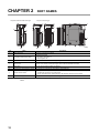
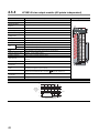
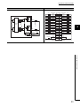
CHAPTER 2
18-point screw terminal block type
PART NAMES
40-pin connector type
1)
2)
1)
2)
1)
2)
1)
7)
3)
4)
6)
6)
5)
1)
8)
8)
No.
8)
Name
Description
1)
Module joint levers
Levers for connecting two modules
2)
I/O operation status indicator LEDs
Indicate the I/O status.
• On (green): I/O signal is on.
• Off: I/O signal is off.
3)
Terminal block
A 18-point terminal block for connecting I/O signal cables to external devices
4)
Terminal cover
A cover for preventing electric shock
A label on it is used for recording the signal names of devices allocated to terminals.
5)
DIN rail hook
A hook used to mount the module to a DIN rail
6)
Connectors for external devices (40 pins)
A connector for connecting I/O signal cables to external devices.
7)
Indication selector switch*1
8)
Serial number display
*1
18
• For input module or output module: Used to switch the LED indications between the first-half 32 points
and latter-half 32 points of a 64-point module.
• For I/O combined module: Used to switch the LED indications between input and output.
Displays the serial number printed on the rating plate.
Operate the Indication selector switch with your fingers. Do not use a screwdriver or similar tool as it may damage the
switch.
CHAPTER 2 PART NAMES
Memo
2
19
CHAPTER 3
3.1
BEFORE USING I/O MODULE
Input Module
(1) Common precautions for all output modules
(a) Simultaneous on points
The number of simultaneous on points of input module depends on the input voltage and ambient temperature.
Refer to the derating chart of the input module specifications. (
Page 28, CHAPTER 4)
(2) Precautions for using the DC input module
(a) Measures against back EMF
When an inductive load is connected, connect a diode in parallel with the load.
Use a diode that meets the following conditions.
• Reverse breakdown voltage is equal to or more than 10 times as large as the circuit voltage.
• Forward current is equal to or more than 2 times as large as the load current.
IN
IN
Inductive
load
Inductive
load
Diode
COM
Positive common
20
Diode
COM
Negative common
CHAPTER 3 BEFORE USING I/O MODULE
3.2
Output Module
(1) Common precautions for all output modules
(a) Maximum switching frequency when the module drives Inductive load.
The output must be on for one second or longer and off for one second or longer.
3
(b) Load for connection
When connecting a counter or timer that has a DC-DC converter as a load, select an output module whose
maximum load current is larger than inrush current of the load.
Selecting an output module by average current of the load may cause a failure of the module because inrush
current flows at a constant frequency at power-on or during operation due to the connected load.
If an output module needs to be selected by average current of the load, take either of the following actions to
reduce an influence from inrush current.
• Connecting a resistor to the load in series
Resistor
Load
Output
module
• Connecting an inductor to the load in series
Inductor Load
Output
module
3.2 Output Module
21
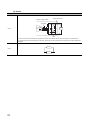
(2) Precaution for using the transistor output module
(a) Action against reverse current
If a transistor output module is wired as shown below, reverse current flows in an output element, causing a
failure of the element.
When wiring a transistor output module, connect a diode as shown below.
• When connecting transistor output modules in parallel
Diode
Load
OUT1
Diode
Load
Diode
Load
OUT1
Diode
Load
OUT2
COM
OUT2
COM
Diode
Diode
OUT1
OUT1
Diode
Diode
OUT2
OUT2
COM
COM
Sink type
Source type
• When incorporating an additional circuit parallel to a transistor output module
Additional circuit
OUT
Additional circuit
OUT
Diode
Diode
COM
COM
Sink type
Source type
(b) Measures against back EMF
When an inductive load is connected, connect a diode in parallel with the load.
Use a diode that meets the following conditions.
• Reverse breakdown voltage is equal to or more than 10 times as large as the circuit voltage.
• Forward current is equal to or more than 2 times as large as the load current.
OUT
Inductive
load
OUT
Diode
COM
Diode
COM
Sink type
22
Inductive
load
Source type
CHAPTER 3 BEFORE USING I/O MODULE
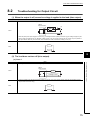
(3) Precautions for using the contact output module
When using the contact output module, consider the following.
• Relay life (contact switching life)
• Effects to relay life due to connected load
• Measures against back EMF
3
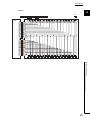
(a) Relay life (contact switching life)
Applicable module LY10R2, LY18R2A
The relay life depends on the operating environment. Select a module according to the operating environment.
The relay lives shown below are the actual service values, not the guaranteed values. Replace the module well
in advance since the actual switching life may be shorter than the one shown below.
200
100
70
50
30
20
Switching life
(10,000 times)
10
3.2 Output Module
7
30VDC
5
=0ms
100VDC
=7ms
100VAC cos =0.7
200VAC cos =0.7
100VAC cos =0.35
3
(L/R) : Time constant
: Power factor
cos
200VAC cos =0.35
24VDC =7ms
2
120VAC cos =0.2
1
0.1
240VAC cos =0.2
0.2
0.3
0.5
0.7
1
2
3
5
Switching current (A)
Operating environment
Rated switching voltage/current, rated load
Switching life
100 thousand times
200VAC 1.5A, 240VAC 1A (COS = 0.7)
100 thousand times
200VAC 0.4A, 240VAC 0.3A (COS = 0.7)
300 thousand times
200VAC 1A, 240VAC 0.5A (COS = 0.35)
100 thousand times
200VAC 0.3A, 240VAC 0.15A (COS = 0.35)
300 thousand times
24VDC 1A, 100VDC 0.1A (L/R = 7ms)
100 thousand times
24VDC 0.3A, 100VDC 0.03A (L/R = 7ms)
300 thousand times
23
(b) Effects to relay life due to connected load
The actual relay life may be significantly shortened compared to the relay life curve, depending on the type of a
load connected and the characteristics of inrush current. (
Page 23, Section 3.2 (3) (a)) Also, the inrush
current may cause the module contact welding.
Take the following measures to prevent shortening of the relay life and the contact welding.
• Select a load so that the inrush current will be within the rated current of the module.
• Connect an external relay that can withstand the inrush current.
The following table shows the relation between the road and the inrush current.
Select a load so that the inrush current (i) and the rated current (io) will be within the rated switching current
specified for the output module used.
The inrush current may flow for a longer time depending on the load.
Load type
Signal waveform diagram
Inrush current
(i)/rated current
(io)
Load of a solenoid
io
Approx. 10 to 20
times
i
i: Inrush current
io: Rated current
0.07 to 0.1 seconds
i
Approx. 3 to 10
times
io
Approx. 3 times*1
i: Inrush current
io: Rated current
180 to 300 seconds
(3 to 5 minutes)
i: Inrush current
io: Rated current
Approx. 0.33 seconds
Lamp load
i: Inrush current
io: Rated current
Load of a mercury lamp
Approx. 3 to 10
times
io
io
0.017 to 0.033 seconds
(1 to 2 cycles)
Load of an incandescent bulb
i
Inrush current
(i)/rated current
(io)
Load of an electromagnetic contactor
i
Inductive load
Signal waveform diagram
Load of a fluorescent
i
io
Approx. 5 to 10
times
Approx. 20 to 40
times
i: Inrush current
io: Rated current
Within 10 seconds
Capacitive load*2
Capacitive load
i
io
i: Inrush current
io: Rated current
0.008 to 0.33 seconds
(0.5 to 2 cycles)
*1
*2
24
Typical electric-discharge lamp circuit includes discharge tubes, transformers, choke coils, and capacitors. Therefore,
note that the inrush current may flow 20 to 40 times as large as the rated current in the case of high power factor and low
power impedance.
When the wiring of the circuit is long, take care of the wire capacity.
CHAPTER 3 BEFORE USING I/O MODULE
(c) Measures against back EMF
Configure a contact protection circuit for extending the contact life, preventing noise when the contact is cut off,
and suppressing the generation of carbide and nitric acid due to arc discharge.
An Incorrect contact protection circuit may cause contact welding.
Also, when using the contact protection circuit, the recovery time may be long.
The following table shows the representative examples of the contact protection circuit.
Example
*1
Capacitor
Inductive
load
Resistor
Capacitor + Resistor
method (CR
method)
Capacitor
Resistor
Diode
Diode + Zener diode
method
Diode
Zener Diode
Inductive
load
Inductive
load
Varistor method
Varistor
*1
Inductive
load
Remarks
Refer to the following for constants of the
capacitor and resistor. Note that the
following values may differ depending on a
nature of the load and a variation of
characteristics of it.
• Capacitor: 0.5 to 1(µF) against load
current of 1A
• Resistor: 0.5 to 1() against power
supply voltage of 1V
Use a capacitor whose withstand voltage is
equal to or more than the rated voltage. In
AC circuit, use a capacitor having no
polarity.
If a load is a relay or solenoid, the recovery
time delays.
A capacitor suppresses electric discharge
while a contact is off, and a resistor
restricts a flow of current while a contact is
on.
Use a diode that meets both conditions
shown below.
• Reverse breakdown voltage is equal to
or more than 10 times as large as the
circuit voltage.
• The forward current is equal to or more
than 2 times as large as the load current.
The recovery time is slower than the CR
method.
Use zener voltage for the zener diode
equal to or more than the power supply
voltage.
This method is effective when the recovery
time delays considerably by the diode
method.
Select a cut voltage (Vc) for the varistor to
meet the following condition.
• Vc > Power voltage × 1.5(V)
• Vc > Power supply voltage × 1.5(V) × √2
(when using AC power supply)
This method is not effective when the Vc is
too high
The recovery time delays slightly.
When using AC power, impedance of CR must be larger enough than it of the load (prevention of a malfunction due to
leak current from the CR).
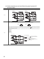
● Avoid providing a contact protection circuits shown below.
These circuit are effective for preventing an arc at shut-off. However, the contact welding may occur because the charge
current flows to capacitor when the contact turns on or off.
A DC inductive load is usually harder for switching than a resistor load, but if a proper protection circuit is configured, the
performance will be similar to the resistor load.
Capacitor
Inductive
load
Capacitor
Inductive
load
● A protection circuit must be provided closely to a load or contact (module). If their distance is far, the protection circuit
may not be effective. Appropriate distance is within 50 cm.
25
3.2 Output Module
Diode method
Inductive
load
3
Method for selecting elements
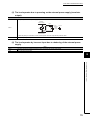
(4) Precautions for using the triac output module
(a) Measures against back EMF
Take measures against back EMF to the side where the load is connected if the wiring distance from the output
module to the load is long.
If not, the surge suppressor in the output module may not work effectively.
Example
Capacitor + Resistor
method (CR
method)
Capacitor
Resistor
Varistor method
Varistor
26
Inductive
load
Inductive
load
Method for selecting elements
Remarks
Refer to the following for constants of the
capacitor and resistor. Note that the
following values may differ depending on a
nature of the load and a variation of
characteristics of it.
• Capacitor: 0.5 to 1(µF) against load
current of 1A
• Resistor: 0.5 to 1() against power
supply voltage of 1V
Use a capacitor whose withstand voltage is
equal to or more than the rated voltage.
Use a capacitor having no polarity.
If a load is a relay or solenoid, the recovery
time delays.
Select a cut-off voltage (Vc) for the varistor
to meet the following condition.
• Vc > Power supply voltage × 1.5(V) × √2
This method is not effective when the Vc is
too high.
The recovery time delays slightly.
CHAPTER 3 BEFORE USING I/O MODULE
3.3
I/O Combined Module
This section describes the precautions for using the I/O combined module.
The precautions not described below are common to that for the input module and output module. (
Page 20,
Section 3.1, Page 21, Section 3.2)
3
(1) I/O numbers of the I/O combined module
The I/O combined module uses same I/O number for input and output.
Because same number is used for input and output, the I/O numbers to be used can be saved.
Input (X)
Output (Y)
X00
Y00
X1F
Y1F
32 points
(2) Applicable software
Use GX Works2 with version 1.492N or later.
The following cannot be set using GX Developer and GX Works2 whose version is earlier than 1.492N.
• "I/O Mix" cannot be selected in I/O Assignment.
• Input response time cannot be set.
• Error Time Output Mode cannot be set.
3.3 I/O Combined Module
27
CHAPTER 4
4.1
SPECIFICATIONS
General Specifications
For the general specifications of the I/O modules, refer to the following manual.
Manual "Safety Guidelines" included in the CPU module or head module
28
CHAPTER 4 SPECIFICATIONS
4.2
Input Module Specifications
4.2.1
LX10 AC input module
Item
Specifications
Number of input points
16 points
Rated input voltage, frequency
100 to 120VAC (+10%/-15%), 50/60Hz(±3Hz)
Input voltage distortion
Within 5%
Rated input current
8.2mA (100VAC, 60Hz), 6.8mA (100VAC, 50Hz)
Inrush current
Max. 200mA within 1ms
ON voltage/ON current
80VAC or higher/5mA or higher (50Hz, 60Hz)
OFF voltage/OFF current
30VAC or lower/1.7mA or lower (50Hz, 60Hz)
Input resistance
12.2k (60Hz), 14.6k (50Hz)
Response time
OFF to ON
ON to OFF
Appearance
4
15ms or less (100VAC 50Hz, 60Hz)
20ms or less (100VAC 50Hz, 60Hz)
Dielectric withstand voltage
1400VAC, 1 minute (altitude 2000m)
Insulation resistance
10M or more by insulation resistance tester
Noise immunity
By noise simulator of 1500Vp-p noise voltage, 1µs noise width and 25 to 60Hz
noise frequency
Protection degree
IP1X
16 points/common (common terminal: TB17)
Number of occupied I/O points
16 points (I/O assignment: input 16 points)
External interface
18-point screw terminal block (M3 × 6 screws) (
5VDC internal current consumption
90mA (TYP. all points ON)
Weight
0.17kg
Page 62, Section 6.2.1)
4.2 Input Module Specifications
Common terminal arrangement
Derating chart
16 points, 50
16 points, 55
16
15 points, 55
12
Simultaneous
on input
8
points
(points)
4
0
Input voltage
50Hz
60Hz
to 132VAC to 120VAC
-
0
to 132VAC
20
40
Ambient temperature(
60
)
29
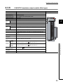
External connections
Terminal connections
LED
TB1
Signal Terminal Signal
name number name
X01
TB16
Photocoupler Internal
circuit
X03
LED
X05
X07
TB17
100 to 120VAC
Photocoupler
X09
X0B
X0D
X0F
2
4
6
8
10
12
14
16
Empty 18
1
3
5
7
9
11
13
15
17
X00
X02
X04
X06
X08
X0A
X0C
X0E
COM
100 to 120VAC
Viewed from the front of the module.
30
CHAPTER 4 SPECIFICATIONS
4.2.2
LX28 AC input module
Item
Specifications
Number of input points
8 points
Rated input voltage, frequency
100 to 240VAC (+10%/-15%), 50/60Hz(±3Hz)
Input voltage distortion
Within 5%
Rated input current
16.4mA (200VAC, 60Hz), 13.7mA (200VAC, 50Hz)
8.2mA (100VAC, 60Hz), 6.8mA (100VAC, 50Hz)
Inrush current
Max. 950mA within 1ms
ON voltage/ON current
80VAC or higher/5mA or higher (50Hz, 60Hz)
OFF voltage/OFF current
30VAC or lower/1.7mA or lower (50Hz, 60Hz)
Input resistance
12.2k (60Hz), 14.6k (50Hz)
Response time
OFF to ON
15ms or less (100VAC 50Hz, 60Hz)
10ms or less (200VAC 50Hz, 60Hz)
ON to OFF
20ms or less (100/200VAC 50Hz, 60Hz)
Appearance
4
Dielectric withstand voltage
2300VAC, 1 minute (altitude 2000m)
Insulation resistance
10M or more by insulation resistance tester
Noise immunity
By noise simulator of 1500Vp-p noise voltage, 1µs noise width and 25 to 60Hz
noise frequency
Protection degree
IP1X
Common terminal arrangement
8 points/common (common terminal: TB17)
Number of occupied I/O points
16 points (I/O assignment: input 16 points)
External interface
18-point screw terminal block (M3 × 6 screws) (
5VDC internal current consumption
80mA (TYP. all points ON)
Weight
0.15kg
Page 62, Section 6.2.1)
Derating chart
4.2 Input Module Specifications
8 points, 50
8 points, 55
8
7 points, 55
6
Simultaneous
on input
4
points
(points)
Input voltage
50Hz
to 200VAC to 132VAC
to 240VAC to 220VAC
2
0
to 264VAC to 264VAC
0
20
40
Ambient temperature (
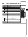
External connections
Photocoupler Internal
circuit
60
)
Terminal connections
LED
TB1
TB15
5 points, 55
60Hz
Terminal Signal
number name
Empty 2
LED
Empty 4
Empty 6
Empty 8
TB17
100 to 240VAC
Photocoupler
Empty 10
Empty 12
Empty 14
Empty 16
Empty 18
1
3
5
7
9
11
13
15
17
X00
X01
X02
X03
X04
X05
X06
X07
COM
100 to 240VAC
Viewed from the front of the module.
31
4.2.3
LX40C6 DC input module
Item
Specifications
Number of input points
16 points
Rated input voltage
24VDC (ripple rate: 5% or less)
(Allowable voltage range: 20.4 to 28.8VDC)
Rated input current
6.0mA TYP. (at 24VDC)
ON voltage/ON current
15V or higher/4mA or higher
OFF voltage/OFF current
8V or lower/2mA or lower
Input resistance
3.8k
Appearance
OFF to ON
1ms, 5ms, 10ms, 20ms, 70ms or less
(PLC parameter setting of CPU module) Initial setting is 10ms.
ON to OFF
1ms, 5ms, 10ms, 20ms, 70ms or less
(PLC parameter setting of CPU module) Initial setting is 10ms.
Response time
Dielectric withstand voltage
510VAC, 1 minute (altitude 2000m)
Insulation resistance
10M or more by insulation resistance tester
Noise immunity
By noise simulator of 500Vp-p noise voltage, 1µs noise width and 25 to 60Hz
noise frequency
Protection degree
IP2X
Common terminal arrangement
16 points/common (common terminal: TB17)
Number of occupied I/O points
16 points (I/O assignment: input 16 points)
External interface
18-point screw terminal block (M3 × 6 screws) (
5VDC internal current consumption
90mA (TYP. all points ON)
Weight
0.15kg
Page 62, Section 6.2.1)
Derating chart
16 points, 50
16 points, 55
16
12
Simultaneous
on input
8
points
(points)
Input voltage
24V DC
26.4V DC
28.8V DC
4
0
32
12 points, 55
16 points, 45
0
20
40
Ambient temperature (
8 points, 55
60
)
CHAPTER 4 SPECIFICATIONS
External connections
Terminal connections
LED
X01
TB1
Photocoupler
24VDC
Internal
circuit
X03
LED
X05
X07
TB16
TB17
Signal Terminal Signal
name number name
Photocoupler
X09
X0B
X0D
X0F
24VDC
2
4
6
8
10
12
14
16
Empty 18
1
3
5
7
9
11
13
15
17
X00
X02
X04
X06
X08
X0A
X0C
X0E
4
COM
24VDC
24VDC
Viewed from the front of the module.
4.2 Input Module Specifications
33
4.2.4
LX41C4 DC input module
Item
Specifications
Number of input points
32 points
Rated input voltage
24VDC (ripple rate: 5% or less)
(Allowable voltage range: 20.4 to 28.8VDC)
Rated input current
4.0mA TYP. (at 24VDC)
ON voltage/ON current
19V or higher/3mA or higher
OFF voltage/OFF current
9V or lower/1.7mA or lower
Input resistance
5.7k
Appearance
OFF to ON
1ms, 5ms, 10ms, 20ms, 70ms or less
(PLC parameter setting of CPU module) Initial setting is 10ms.
ON to OFF
1ms, 5ms, 10ms, 20ms, 70ms or less
(PLC parameter setting of CPU module) Initial setting is 10ms.
Response time
Dielectric withstand voltage
510VAC, 1 minute (altitude 2000m)
Insulation resistance
10M or more by insulation resistance tester
Noise immunity
By noise simulator of 500Vp-p noise voltage, 1µs noise width and 25 to 60Hz
noise frequency
Protection degree
IP2X
Common terminal arrangement
32 points/common (common terminal: B01, B02)
Number of occupied I/O points
32 points (I/O assignment: input 32 points)
External interface
40-pin connector (
5VDC internal current consumption
100mA (TYP. all points ON)
Weight
0.11kg
Page 64, Section 6.2.2)
Derating chart
32 points, 50
32 points, 40
32 points, 55
30
24 points, 55
Simultaneous
20
on input
points
(points)
10
0
20 points, 55
Input voltage
24V DC
26.4V DC
28.8V DC
0
20
40
Ambient temperature(
34
60
)
CHAPTER 4 SPECIFICATIONS
External connections
Terminal connections
Signal
name
LED
X00
X01
B20
Photocoupler
Internal
circuit
X02
X03
LED
X04
X05
X06
A05
B01,B02
X07
Photocoupler
X08
X09
24VDC
X0A
X0B
X0C
24VDC
X0D
X0E
X0F
Pin
number
B20
A20
B19
A19
B18
A18
B17
A17
B16
A16
B15
A15
B14
A14
B13
A13
B12
A12
B11
A11
B10
A10
B09
A09
B08
A08
B07
A07
B06
A06
Signal
name
X10
X11
X12
X13
X14
X15
X16
X17
X18
X19
X1A
X1B
X1D
X1E
X1F
B05
A05
Empty
B04
A04
Empty
Empty
COM
B03
A03
Empty
B02
A02
Empty
B01
A01
Empty
COM
4
X1C
24VDC
24VDC
Viewed from the front of
the module.
4.2 Input Module Specifications
35
4.2.5
LX42C4 DC input module
Item
Specifications
Number of input points
64 points
Rated input voltage
24VDC (ripple rate: 5% or less)
(Allowable voltage range: 20.4 to 28.8VDC)
Rated input current
4.0mA TYP. (at 24VDC)
ON voltage/ON current
19V or higher/3mA or higher
OFF voltage/OFF current
9V or lower/1.7mA or lower
Input resistance
5.7k
Appearance
OFF to ON
1ms, 5ms, 10ms, 20ms, 70ms or less
(PLC parameter setting of CPU module) Initial setting is 10ms.
ON to OFF
1ms, 5ms, 10ms, 20ms, 70ms or less
(PLC parameter setting of CPU module) Initial setting is 10ms.
Response time
Dielectric withstand voltage
510VAC, 1 minute (altitude 2000m)
Insulation resistance
10M or more by insulation resistance tester
Noise immunity
By noise simulator of 500Vp-p noise voltage, 1µs noise width and 25 to 60Hz
noise frequency
Protection degree
IP2X
Common terminal arrangement
32 points/common (common terminal: 1B01, 1B02, 2B01, 2B02)
Number of occupied I/O points
64 points (I/O assignment: input 64 points)
External interface
40-pin connector (
5VDC internal current consumption
120mA (TYP. all points ON)
Weight
0.12kg
Page 64, Section 6.2.2)
Derating chart
64 points, 10
64 points, 24
64 points, 35
16 points/common
(total 32 points), 55
60
11 points/common
(total 22 points), 55
Simultaneous
40
ON point
(points)
Input voltage
9 points/common
(total 18 points), 55
24V DC
26.4V DC
28.8V DC
20
0
0
36
20
40
Ambient temperature(
60
)
CHAPTER 4 SPECIFICATIONS
External connections
Terminal connections
Left side connector
Signal
name
1B20
Photocoupler
Internal
circuit
X00
LED
X01
X02
X03
X04
1A05
X05
Photocoupler
1B01,1B02
Left side connectors
(first half )
Right side connectors
(last half )
X06
X07
sw Indication
1
X08
selector
circuit
X09
X0A
X0B
24VDC
The above diagram shows the first half of 32 points (F).
The last half of 32 points (L) are similar.
X0C
X0D
X0E
24VDC
X0F
Pin
number
1B20
1A20
1B19
1A19
1B18
1A18
1B17
1A17
1B16
1A16
1B15
1A15
1B14
1A14
1B13
1A13
1B12
1A12
1B11
1A11
1B10
1A10
1B09
1A09
1B08
1A08
1B07
1A07
1B06
1A06
Signal
name
X10
X20
X11
X21
X12
X22
X13
X23
X14
X24
X15
X25
X16
X26
X17
X27
X18
X28
X19
X29
X1A
X2A
X1B
X2B
X1C
X2C
X1D
X2D
X1E
X2E
X1F
X2F
Pin
number
2B20
2A20
2B19
2A19
2B18
2A18
2B17
2A17
2B16
2A16
2B15
2A15
2B14
2A14
2B13
2A13
2B12
2A12
2B11
2A11
2B10
2A10
2B09
2A09
2B08
2A08
2B07
2A07
2B06
2A06
2B05
2A05
Signal
name
X30
X31
X32
X33
X34
X35
X36
X37
X38
X39
X3A
X3D
X3E
X3F
1A05
1B04
1A04 Empty
Empty 2B04
2A04 Empty
Empty 1B03
COM1
1B02
COM1
1B01
1A03 Empty
Empty 2B03
COM2
2B02
COM2
2B01
2A03 Empty
1A02 Empty
1A01 Empty
24VDC
4
X3B
X3C
1B05
Empty
2A02 Empty
2A01 Empty
24VDC
24VDC
24VDC
Viewed from the front of
the module.
*1
Right side connectors
Signal
name
Viewed from the front of
the module.
Switching left side (F) provides the first half (X00 to X1F) LED indications, and switching right side (L) provides the latter
half (Y20 to Y3F) LED indications.
4.2 Input Module Specifications
37
4.3
Output Module Specifications
The following output module equips the overload protection function and the overheat protection function.
Applicable model LY40NT5P, LY41NT1P, LY42NT1P, LY40PT5P, LY41PT1P, LY42PT1P
Function
Description
Overload protection function*1
• If the output module detects overcurrent, it limits output current by the current limiter operation*2
• For the overcurrent detection value and the limited current, refer to "Overload protection function" on the
module specifications.
• When the load current becomes lower than the overcurrent detection value, the module returns to normal
operation.
Overheat protection function*1
• If overcurrent keeps flowing due to overload, heat is generated inside the module. When high heat is
detected inside the module, the output is turned off.
• The number of output points that the overheat protection function simultaneously operates differs depending
on the module. For the number, refer to "Overheat protection function" on the module specifications.
• After heat goes down, the module returns to normal operation.
*1
*2
38
This function is for protecting the internal circuit of the module, not for protecting external devices.
Also, leaving the failure too long may rise the internal temperature of the module, resulting in deterioration of output
elements and/or discoloration of a case and printed circuit board. When the failure occurs, turn off the corresponding
outputs immediately to remove the causes.
This operation limits overcurrent to a constant value and keeps outputting it.
CHAPTER 4 SPECIFICATIONS
4.3.1
LY10R2 contact output module
Item
Specifications
Number of output points
16 points
Rated switching voltage, current
24VDC 2A (resistance load)/point, 8A/common
240VAC 2A (COS = 1)/point, 8A/common
Minimum switching load
5VDC 1mA
Maximum switching load
264VAC 125VDC
Response time
Life
OFF to ON
10ms or less
ON to OFF
12ms or less
Mechanical
20 million times or more
Electrical
Appearance
4
Page 23, Section 3.2 (3) (a)
Maximum switching frequency
3600 times/hour
Surge suppressor
None
Fuse
None
Dielectric withstand voltage
2300VAC, 1 minute (altitude 2000m)
Insulation resistance
10M or more by insulation resistance tester
Noise immunity
By noise simulator of 1500Vp-p noise voltage, 1µs noise width and 25 to 60Hz
noise frequency
Protection degree
IP1X
Common terminal arrangement
16 points/common (common terminal: TB17)
Number of occupied I/O points
16 points (I/O assignment: output 16 points)
External interface
18-point screw terminal block (M3 × 6 screws) (
5VDC internal current
consumption
460mA (TYP. all points ON)
Weight
0.21kg
Page 62, Section 6.2.1)
Terminal connections
Signal
name
Load
Load
Load
LED
TB1
Load
Load
Load
Load
LED
Internal
circuit
4.3 Output Module Specifications
External connections
Load
Relay
TB16 Load
Load
Terminal Signal
number name
1
2
3
4
5
6
7
8
9
10
11
12
13
14
15
16
17
Empty 18
Y01
Y03
Y05
Y07
Y09
Y0B
Y0D
Y0F
Y00
Y02
Y04
Y06
Y08
Y0A
Y0C
Y0E
COM
Load
Load
Load
Load
Load
Load
Load
Load
External load
power supply
TB17
Relay
100/200VAC
or
24VDC
Viewed from the front of the module.
The following diagram shows the external load power supply.
100/200VAC
or
24VDC
39
4.3.2
LY18R2A contact output module (All points independent)
Item
Specifications
Number of output points
8 points
Insulation method
Relay
Rated switching voltage, current
24VDC 2A (resistance load)/point, 8A/module
240VAC 2A (COS = 1)/point, 8A/module
Minimum switching load
5VDC 1mA
Maximum switching load
264VAC 125VDC
Response time
Life
OFF to ON
Appearance
10ms or less
ON to OFF
12ms or less
Mechanical
20 million times or more
Electrical
Page 23, Section 3.2 (3) (a)
Maximum switching frequency
3600 times/hour
Surge suppressor
None
Fuse
None (Attaching a fuse to each external wiring is recommended.)
Dielectric withstand voltage
2300VAC, 1 minute (altitude 2000m)
Insulation resistance
10M or more by insulation resistance tester
Noise immunity
By noise simulator of 1500Vp-p noise voltage, 1µs noise width and 25 to 60Hz
noise frequency
Protection degree
IP1X
Common terminal arrangement
No common (all-point independent contact)
Number of occupied I/O points
16 points (I/O assignment: output 16 points)
External interface
18-point screw terminal block (M3 × 6 screws) (
5VDC internal current
consumption
260mA (TYP. all points ON)
Weight
0.18kg
External connections
Page 62, Section 6.2.1)
Terminal connections
Signal Terminal
name number
External load power supply
TB1
LED
Load
External load power supply
External load power supply
External load power supply
TB2
External load power supply
Relay
100/200VAC
or
24VDC
Internal
circuit
External load power supply
External load power supply
External load power supply
TB15
LED
Y00
Y01
Y02
Y03
Y04
Y05
Y06
Y07
1
2
3
4
5
6
7
8
9
10
11
12
13
14
15
16
Empty 18
Load
17
Signal
name
Y00
Load
Y01
Load
Y02
Load
Y03
Load
Y04
Load
Y05
Load
Y06
Load
Y07
Load
Empty
TB16
Relay
100/200VAC
or
24VDC
Viewed from the front of the module.
The following diagram shows the external load power supply.
100/200VAC
or 24VDC
40
CHAPTER 4 SPECIFICATIONS
4.3.3
LY20S6 triac output module
Item
Specifications
Number of output points
16 points
Rated load voltage,
frequency
100 to 240VAC (+10%/-15%), 50/60Hz(±3Hz)
Maximum load current
0.6A/point, 4.8A/common
Appearance
Load voltage distortion ratio
Within 5%
Maximum load voltage
264VAC
Minimum load
voltage/current
24VAC/100mA, 100VAC/25mA, 240VAC/25mA
Maximum inrush current
20A/cycle or less
Leakage current at OFF
3mA or lower (at 240V, 60Hz), 1.5mA or lower (at 120V, 60Hz)
Maximum voltage drop at ON
1.5V or lower (at load current of 0.6A)
Response
time
OFF to ON
ON to OFF
Surge suppressor
4
Total of 1ms and 0.5 cycles or less
Total of 1ms and 0.5 cycles or less (rated load, resistive load)
CR absorber
None (Attaching a fuse to each external wiring is recommended.)
Dielectric withstand voltage
2300VAC, 1 minute (altitude 2000m)
Insulation resistance
10M or more by insulation resistance tester
Noise immunity
By noise simulator of 1500Vp-p noise voltage, 1µs noise width and 25 to 60Hz noise
frequency
Protection degree
IP1X
Common terminal
arrangement
16 points/common (common terminal: TB17)
Number of occupied I/O
points
16 points (I/O assignment: output 16 points)
External interface
18-point screw terminal block (M3 × 6 screws)(
5VDC internal current
consumption
300mA (TYP. all points ON)
Weight
0.22kg
Page 62, Section 6.2.1)
External connections
Terminal connections
Signal
name
TB1 Load
LED
Load
Load
Load
Load
LED
Internal
circuit
4.3 Output Module Specifications
Fuse
TB16 Load
Load
Load
Load
Load
TB17
100 to 240VAC
Terminal Signal
number name
1
2
3
Y03
4
5
Y05
6
7
Y07
8
9
Y09
10
11
Y0B
12
13
Y0D
14
15
Y0F
16
17
Empty 18
Y01
Y00
Load
Y02
Load
Y04
Load
Y06
Load
Y08
Load
Y0A
Load
Y0C
Load
Y0E
Load
COM
100 to 240VAC
Viewed from the front of the module.
41
4.3.4
LY28S1A triac output module (All points independent)
Item
Specifications
Number of output points
8 points
Insulation method
Photocoupler isolation
Rated load voltage,
frequency
100 to 240VAC (+10%/-15%), 50/60Hz(±3Hz)
Maximum load current
1A/point, 8A/module
Load voltage distortion ratio
Within 5%
Maximum load voltage
264VAC
Minimum load
voltage/current
24VAC/100mA, 100VAC/25mA, 240VAC/25mA
Appearance
Maximum inrush current
20A/cycle or less
Leakage current at OFF
3mA or lower (at 240V, 60Hz), 1.5mA or lower (at 120V, 60Hz)
Maximum voltage drop at ON
1.5V or lower (at load current of 0.6A)
Response
time
OFF to ON
Total of 1ms and 0.5 cycles or less
ON to OFF
Total of 1ms and 0.5 cycles or less (rated load, resistive load)
Surge suppressor
CR absorber
Fuse
None (Attaching a fuse to each external wiring is recommended.)
Dielectric withstand voltage
2300VAC, 1 minute (altitude 2000m)
Insulation resistance
10M or more by insulation resistance tester
Noise immunity
By noise simulator of 1500Vp-p noise voltage, 1µs noise width and 25 to 60Hz noise
frequency
Protection degree
IP1X
Common terminal
arrangement
No common (all points independent)
Number of occupied I/O
points
16 points (I/O assignment: output 16 points)
External interface
18-point screw terminal block (M3 × 6 screws) (
5VDC internal current
consumption
200mA (TYP. all points ON)
Weight
0.19kg
Page 62, Section 6.2.1)
Derating chart
8A, 45
8
6
Module
total output
4
current
(A)
2
0
42
3A, 55
Load voltage
132VAC/264VAC
0
20
40
Ambient temperature ()
60
CHAPTER 4 SPECIFICATIONS
External connections
Terminal connections
TB1
LED
Signal Terminal
name number
Load
External load power supply
External load power supply
External load power supply
External load power supply
TB2
External load power supply
100 to 240VAC
Internal
circuit
External load power supply
External load power supply
External load power supply
LED
TB15
Load
TB16
Y00
Y01
Y02
Y03
Y04
Y05
Y06
Y07
1
2
3
4
5
6
7
8
9
10
11
12
13
14
15
16
Empty 18
17
Signal
name
Y00
Load
Y01
Load
Y02
Load
Y03
Load
Y04
Load
Y05
Load
Y06
Load
Y07
Load
Empty
4
Viewed from the front of the module.
The following diagram shows the external load power supply.
100 to 240VAC
100 to 240VAC
4.3 Output Module Specifications
43
4.3.5
LY40NT5P transistor output module (Sink type)
Item
Specifications
Number of output points
16 points
Rated load voltage
10.2 to 28.8VDC
Maximum load current
0.5A/point, 5A/common
Maximum inrush current
Current is limited by the overload protection function.
Leakage current at OFF
0.1mA or less
Maximum voltage drop at ON
0.2VDC (TYP.) 0.5A, 0.3VDC (MAX.) 0.5A
Response
time
OFF to ON
0.5ms or less
ON to OFF
1ms or less (rated load, resistance load)
Surge suppressor
Zener diode
Fuse
None
External
power
supply
Appearance
Voltage
12/24VDC (ripple rate: 5% or less) (Allowable voltage range: 10.2 to 28.8VDC)
Current
9mA (at 24VDC)/common
Dielectric withstand voltage
510VAC, 1 minute (altitude 2000m)
Insulation resistance
10M or more by insulation resistance tester
Noise immunity
By noise simulator of 500Vp-p noise voltage, 1µs noise width and 25 to 60Hz noise
frequency
Protection degree
IP2X
Common terminal
arrangement
16 points/common (common terminal: TB18)
Number of occupied I/O
points
16 points (I/O assignment: output 16 points)
Protection
function
Overload
protection
function
Overheat
protection
function
Limited current when detecting overcurrent (overload protection): 1.5 to 3.5A/point
Activated in increments of 1 point. (
Page 38, Section 4.3)
Activated in increments of 1 point. (
Page 38, Section 4.3)
External interface
18-point screw terminal block (M3 × 6 screws)(
5VDC internal current
consumption
100mA (TYP. all points ON)
Weight
0.15kg
Page 62, Section 6.2.1)
External connections
LED
Terminal connections
Signal
name
Terminal Signal
number name
Load
Y01
Load
Y03
Load
Y05
1
2
3
4
5
6
7
8
9
10
11
12
13
14
15
16
17
18
Load
TB1
Photocoupler
Internal
circuit
LED
TB16
Load
Photocoupler
Constant-voltage
circuit
Load
Y07
Load
Y09
Load
Y0B
Load
Y0D
Load
Y0F
TB17
COM
Y00
Load
Y02
Load
Y04
Load
Y06
Load
Y08
Load
Y0A
Load
Y0C
Load
Y0E
Load
+V (12/24VDC)
TB18
12/24VDC
12/24VDC
Viewed from the front of the module.
44
CHAPTER 4 SPECIFICATIONS
4.3.6
LY41NT1P transistor output module (Sink type)
Item
Specifications
Number of output points
32 points
Rated load voltage
10.2 to 28.8VDC
Maximum load current
0.1A/point, 2A/common
Maximum inrush current
Current is limited by the overload protection function.
Leakage current at OFF
0.1mA or less
Maximum voltage drop at ON
0.1VDC (TYP.) 0.1A, 0.2VDC (MAX.) 0.1A
Response
time
OFF to ON
0.5ms or less
ON to OFF
1ms or less (rated load, resistance load)
Surge suppressor
Zener diode
Fuse
None
External
power
supply
4
Voltage
12/24VDC (ripple rate: 5% or less) (Allowable voltage range: 10.2 to 28.8VDC)
Current
13mA (at 24VDC)
Dielectric withstand voltage
510VAC, 1 minute (altitude 2000m)
Insulation resistance
10M or more by insulation resistance tester
Noise immunity
By noise simulator of 500Vp-p noise voltage, 1µs noise width and 25 to 60Hz noise
frequency
Protection degree
IP2X
Common terminal
arrangement
32 points/common (common terminal: A01, A02)
Number of occupied I/O
points
32 points (I/O assignment: output 32 points)
Overheat
protection
function
Limited current when detecting overcurrent (overload protection): 1 to 3A/point
Activated in increments of 1 point. (
Page 38, Section 4.3)
Activated in increments of 1 point. (
Page 38, Section 4.3)
External interface
40-pin connector (
5VDC internal current
consumption
140mA (TYP. all points ON)
Weight
0.11kg
4.3 Output Module Specifications
Protection
functions
Overload
protection
function
Appearance
Page 64, Section 6.2.2)
45
External connections
Terminal connections
Signal
Signal
Pin
name number name
Load
Y00
Load
Y01
Load
LED
Load
B20
Load
Load
Load
Load
Internal
circuit
Photocoupler
Load
Load
Load
LED
A05
Load
Load
Load
Load
Load
Photocoupler
Load
Load
Constant-voltage
circuit
B01,B02
Y02
Y03
Y04
Y05
Y06
Y07
Y08
Y09
Y0A
Y0B
Y0C
Y0D
Y0E
Y0F
B20
A20
B19
A19
B18
A18
B17
A17
B16
A16
B15
A15
B14
A14
B13
A13
B12
A12
B11
A11
B10
A10
B09
A09
B08
A08
B07
A07
B06
A06
B05
A05
Empty B04
Empty B03
12/24VDC
B02
12/24VDC
B01
A01,A02
Y10
Load
Y11
Load
Y12
Load
Y13
Load
Y14
Load
Y15
Load
Y16
Load
Y17
Load
Y18
Load
Y19
Load
Y1A
Load
Y1B
Load
Y1C
Load
Y1D
Load
Y1E
Load
Y1F
Load
A04 Empty
A03 Empty
A02
COM
COM
A01
12/24VDC
12/24VDC
Viewed from the front of
the module.
46
CHAPTER 4 SPECIFICATIONS
4.3.7
LY42NT1P transistor output module (Sink type)
Item
Specifications
Number of output points
64 points
Rated load voltage
10.2 to 28.8VDC
Maximum load current
0.1A/point, 2A/common
Maximum inrush current
Current is limited by the overload protection function.
Leakage current at OFF
0.1mA or less
Maximum voltage drop at ON
0.1VDC (TYP.) 0.1A, 0.2VDC (MAX.) 0.1A
Response
time
OFF to ON
0.5ms or less
ON to OFF
1ms or less (rated load, resistance load)
Surge suppressor
Zener diode
Fuse
None
External
power
supply
4
Voltage
12/24VDC (ripple rate: 5% or less) (Allowable voltage range: 10.2 to 28.8VDC)
Current
9mA (at 24VDC)/common
Dielectric withstand voltage
510VAC, 1 minute (altitude 2000m)
Insulation resistance
10M or more by insulation resistance tester
Noise immunity
By noise simulator of 500Vp-p noise voltage, 1µs noise width and 25 to 60Hz noise
frequency
Protection degree
IP2X
Common terminal
arrangement
32 points/common (common terminal: 1A01, 1A02, 2A01, 2A02)
Number of occupied I/O
points
64 points (I/O assignment: output 64 points)
Overheat
protection
function
Limited current when detecting overcurrent (overload protection): 1 to 3A/point
Activated in increments of 1 point. (
Activated in increments of 1 points. (
External interface
40-pin connector (
5VDC internal current
consumption
190mA (TYP. all points ON)
Weight
0.12kg
Page 38, Section 4.3)
4.3 Output Module Specifications
Protection
function
Overload
protection
function
Appearance
Page 38, Section 4.3)
Page 64, Section 6.2.2)
47
External connections
Terminal connections
1B20
Load
Y00
Load
Y01
Load
Load
Internal
circuit
Photocoupler
Load
Load
Load
1A05
Load
Load
Load
Load
Load
Photocoupler
Indication
selector
circuit
Load
Left side connectors
(first half )
sw
Right side connectors
(last half )
*1
Load
Constant-voltage
circuit
1B01,1B02
1A01,1A02
The above diagram shows the first half of 32 points (F).
The last half of 32 points (L) are similar.
12/24VDC
Right side connectors
Signal
Signal
Pin
name number name
Load
Load
LED
Left side connector
Signal
Signal
Pin
name number name
Load
Load
Y02
Y03
Y04
Y05
Y06
Y07
Y08
Y09
Y0A
Y0B
Y0C
Y0D
Y0E
Y0F
1B20 1A20
1B19 1A19
1B18 1A18
1B17 1A17
1B16 1A16
1B15 1A15
1B14 1A14
1B13 1A13
1B12 1A12
1B11 1A11
1B10 1A10
1B09 1A09
1B08 1A08
1B07 1A07
1B06 1A06
1B05 1A05
Y10
Load
Load
Y20
Y11
Load
Load
Y21
Y12
Load
Y13
Load
Y14
Load
Y15
Load
Y16
Load
Y17
Load
Y18
Load
Y19
Load
Y1A
Load
Y1B
Load
Y1C
Load
Y1D
Load
Y1E
Load
Y1F
Load
Load
Load
Load
Load
Load
Load
Load
Load
Load
Load
Load
Load
Load
Load
Y22
Y23
Y24
Y25
Y26
Y27
Y28
Y29
Y2A
Y2B
Y2C
Y2D
Y2E
Y2F
2B20 2A20
2B19 2A19
2B18 2A18
2B17 2A17
2B16 2A16
2B15 2A15
2B14 2A14
2B13 2A13
2B12 2A12
2B11 2A11
2B10 2A10
2B09 2A09
2B08 2A08
2B07 2A07
2B06 2A06
2B05 2A05
Y30
Load
Y31
Load
Y32
Load
Y33
Load
Y34
Load
Y35
Load
Y36
Load
Y37
Load
Y38
Load
Y39
Load
Y3A
Load
Y3B
Load
Y3C
Load
Y3D
Load
Y3E
Load
Y3F
Load
Empty 2B04 2A04 Empty
Empty 2B03 2A03 Empty
12/24VDC
COM2
2B02 2A02
COM2
12/24VDC
2B01 2A01
Empty 1B04 1A04 Empty
Empty 1B03 1A03 Empty
12/24VDC
COM1
1B02 1A02
COM1
12/24VDC
1B01 1A01
12/24VDC
Viewed from the front of
the module.
*1
48
12/24VDC
Viewed from the front of
the module.
Switching left side (F) provides the first half (Y00 to Y1F) LED indications, and switching right side (L) provides the latter
half (Y20 to Y3F) LED indications.
CHAPTER 4 SPECIFICATIONS
4.3.8
LY40PT5P transistor output module (Source type)
Item
Specifications
Number of output points
16 points
Rated load voltage
10.2 to 28.8VDC
Maximum load current
0.5A/point, 5A/common
Maximum inrush current
Current is limited by the overload protection function.
Leakage current at OFF
0.1mA or less
Maximum voltage drop at ON
0.2VDC (TYP.) 0.5A, 0.3VDC (MAX.) 0.5A
Response
time
OFF to ON
0.5ms or less
ON to OFF
1ms or less (rated load, resistance load)
Surge suppressor
Zener diode
Fuse
None
External
power
supply
Appearance
4
Voltage
12/24VDC (ripple rate: 5% or less) (Allowable voltage range: 10.2 to 28.8VDC)
Current
17mA (at 24VDC)
Dielectric withstand voltage
510VAC, 1 minute (altitude 2000m)
Insulation resistance
10M or more by insulation resistance tester
Noise immunity
By noise simulator of 500Vp-p noise voltage, 1µs noise width and 25 to 60Hz noise
frequency
Protection degree
IP2X
Common terminal
arrangement
16 points/common (common terminal: TB17)
Number of occupied I/O
points
16 points (I/O assignment: output 16 points)
Overheat
protection
function
Overcurrent detection: 1.5A or more/point
Activated in increments of 1 point. (
Page 38, Section 4.3)
Activated in increments of 1 point. (
Page 38, Section 4.3)
External interface
18-point screw terminal block (M3 × 6 screws)(
5VDC internal current
consumption
100mA (TYP. all points ON)
Weight
0.15kg
Page 62, Section 6.2.1)
External connections
Terminal connections
Load
LED
TB1
LED
TB16
Load
12/24VDC
Constant-voltage
circuit
TB17
TB18
Terminal Signal
number name
Y01
1
2
3
4
5
6
7
8
9
10
11
12
13
14
15
16
17
18
Y03
Load
Y05
Load
Y07
Photocoupler
Internal
circuit
Signal
name
Load
Load
Photocoupler
4.3 Output Module Specifications
Protection
function
Overload
protection
function
Load
Y09
Load
Y0B
Load
Y0D
Load
Y0F
0V
Y00
Load
Y02
Load
Y04
Load
Y06
Load
Y08
Load
Y0A
Load
Y0C
Load
Y0E
Load
COM
12/24VDC
Viewed from the front of the module.
49
4.3.9
LY41PT1P transistor output module (Source type)
Item
Specifications
Number of output points
32 points
Rated load voltage
10.2 to 28.8VDC
Max. load current
0.1A/point, 2A/common
Max. inrush current
Current is limited by the overload protection function.
Leakage current at OFF
0.1mA or less
Maximum voltage drop at ON
0.1VDC (TYP.) 0.1A, 0.2VDC (MAX.) 0.1A
Response
time
OFF to ON
ON to OFF
0.5ms or less
1ms or less (rated load, resistance load)
Surge suppressor
Zener diode
Fuse
None
External
power
supply
Voltage
12/24VDC (ripple rate: 5% or less) (Allowable voltage range: 10.2 to 28.8VDC)
Current
20mA (at 24VDC)
Dielectric withstand voltage
510VAC, 1 minute (altitude 2000m)
Insulation resistance
10M or more by insulation resistance tester
Noise immunity
By noise simulator of 500Vp-p noise voltage, 1µs noise width and 25 to 60Hz noise
frequency
Protection degree
IP2X
Common terminal
arrangement
32 points/common (common terminal: B01, B02)
Number of occupied I/O
points
32 points (I/O assignment: output 32 points)
Protection
function
Overload
protection
function
Overheat
protection
function
Limited current when detecting overcurrent (overload protection): 1 to 3A/point
Activated in increments of 1 point. (
Activated in increments of 2 points. (
External interface
40-pin connector (
5VDC internal current
consumption
140mA (TYP. all points ON)
Weight
0.11kg
50
Page 38, Section 4.3)
Page 38, Section 4.3)
Page 64, Section 6.2.2)
Appearance
CHAPTER 4 SPECIFICATIONS
External connections
Terminal connections
Load
LED
TB20
Load
Photocoupler
Internal
circuit
LED
A05
Load
Photocoupler
12/24VDC
Constant-voltage
circuit
B01,B02
Signal name
Y00
Load
Y01
Load
Y02
Load
Y03
Load
Y04
Load
Y05
Load
Y06
Load
Y07
Load
Y08
Load
Y09
Load
Y0A
Load
Y0B
Load
Y0C
Load
Y0D
Load
Y0E
Load
Y0F
A01,B02
12/24VDC
Pin number
B20
B19
B18
B17
B16
B15
A20
A19
A18
A17
A16
A15
B14
A14
B13
A13
B12
B11
B10
B09
A12
A11
A10
A09
B08
A08
B07
A07
B06
A06
Signal name
Y10
Load
Y11
Load
Y12
Load
Y13
Load
Y14
Load
Y15
Load
Y16
Load
Y17
Load
Y18
Load
Y19
Load
Y1A
Load
Y1B
Load
Y1C
Load
Y1D
Load
Y1E
Load
Y1F
Load
B05
A05
Empty
B04
A04
Empty
Empty
B03
A03
Empty
B02
A02
B01
A01
COM
COM
4
0V
0V
Viewed from the front of the module.
4.3 Output Module Specifications
51
4.3.10
LY42PT1P transistor output module (Source type)
Item
Specifications
Number of output points
64 points
Rated load voltage
10.2 to 28.8VDC
Appearance
Max. load current
0.1A/point, 2A/common
Max. inrush current
Current is limited by the overload protection function.
Leakage current at OFF
0.1mA or less
Maximum voltage drop at ON
0.1VDC (TYP.) 0.1A, 0.2VDC (MAX.) 0.1A
Response
time
OFF to ON
0.5ms or less
ON to OFF
1ms or less (rated load, resistance load)
Surge suppressor
Zener diode
Fuse
None
External
power
supply
Voltage
12/24VDC (ripple rate: 5% or less) (Allowable voltage range: 10.2 to 28.8VDC)
Current
20mA (at 24VDC)/common
Dielectric withstand voltage
510VAC, 1 minute (altitude 2000m)
Insulation resistance
10M or more by insulation resistance tester
Noise immunity
By noise simulator of 500Vp-p noise voltage, 1µs noise width and 25 to 60Hz noise
frequency
Protection degree
IP2X
Common terminal arrangement
32 points/common (common terminal: 1B01, 1B02, 2B01, 2B02)
Number of occupied I/O points
Protection
function
Overload
protection function
Overheat
protection function
64 points (I/O assignment: output 64 points)
Limited current when detecting overcurrent (overload protection): 1 to 3A/point
Activated in increments of 1 point. (
Page 38, Section 4.3)
Activated in increments of 2 point. (
Page 38, Section 4.3)
External interface
40-pin connector (
5VDC internal current
consumption
190mA (TYP. all points ON)
Weight
0.12kg
Page 64, Section 6.2.2)
External connections
Terminal connections
Left side connector
Signal
Pin
Signal
name number name
Load
Y00
Load
Y01
Load
1B20
Load
Load
Load
LED
Photocoupler
Load
Load
Internal
circuit
Load
Load
Load
Load
1A05
Load
Load
Load
Load
Photocoupler
Left side connectors
(first half )
Indication
sw
selector
Right side connectors
circuit
(last half )
Constant-voltage
circuit
12/24VDC
1B01,1B02
1A01.1A02
*1
The above diagram shows the first half of 32 points (F).
The last half of 32 points (L) are similar.
Load
Load
Y02
Y03
Y04
Y05
Y06
Y07
Y08
Y09
Y0A
Y0B
Y0C
Y0D
Y0E
Y0F
1B20 1A20
1B19 1A19
1B18 1A18
1B17 1A17
1B16 1A16
1B15 1A15
1B14 1A14
1B13 1A13
1B12 1A12
1B11 1A11
1B10 1A10
1B09 1A09
1B08 1A08
1B07 1A07
1B06 1A06
1B05 1A05
Empty 1B04
Empty 1B03
COM1
1B02
COM1
1B01
Y10
Load
Load
Y11
Load
Load
Y21
Y12
Load
Load
Y22
Y13
Load
Load
Y23
Y14
Load
Load
Y24
Y15
Load
Load
Y25
Y16
Load
Load
Y26
Y17
Load
Load
Y27
Y18
Load
Load
Y28
Y19
Load
Load
Y29
Y1A
Load
Load
Y2A
Y1B
Load
Load
Y2B
Y1C
Load
Load
Y2C
Y1D
Load
Load
Y2D
Y1E
Load
Load
Y2E
Y1F
Load
Load
Y2F
1A04 Empty
1A03 Empty
0V
1A02
0V
1A01
12/24VDC
Viewed from the front of the module.
*1
52
Right side connectors
Signal
Pin
Signal
name number name
Y20
2B20 2A20
2B19 2A19
2B18 2A18
2B17 2A17
2B16 2A16
2B15 2A15
2B14 2A14
2B13 2A13
2B12 2A12
2B11 2A11
2B10 2A10
2B09 2A09
2B08 2A08
2B07 2A07
2B06 2A06
2B05 2A05
Empty 2B04
Empty 2B03
COM2
2B02
COM2
2B01
Y30
Load
Y31
Load
Y32
Load
Y33
Load
Y34
Load
Y35
Load
Y36
Load
Y37
Load
Y38
Load
Y39
Load
Y3A
Load
Y3B
Load
Y3C
Load
Y3D
Load
Y3E
Load
Y3F
Load
2A04 Empty
2A03 Empty
0V
2A02
0V
2A01
12/24VDC
Viewed from the front of the module.
Switching left side (F) provides the first half (Y00 to Y1F) LED indications, and switching right side (L) provides the latter
half (Y20 to Y3F) LED indications.
CHAPTER 4 SPECIFICATIONS
4.4
I/O Combined Module Specifications
The I/O combined module equips the overload protection function and the overheat protection function.
Function
Description
Overload protection function*1
• If the output side detects overcurrent, it limits output current by the current limiter operation *2
• For the overcurrent detection value and the limited current, refer to "Overload protection function" on the
module specifications.
• When the load current becomes lower than the overcurrent detection value, the module returns to normal
operation.
Overheat protection function*1
• If overcurrent keeps flowing due to overload on the output side, heat is generated inside the module. When
high heat is detected inside the module, the output is turned off.
• The number of output points that the overheat protection function simultaneously operates differs depending
on the module. For the number, refer to "Overheat protection function" on the module specifications.
• After heat goes down, the module returns to normal operation.
*1
*2
4
This function is for protecting the internal circuit of the module, not for protecting external devices.
Also, leaving the failure too long may rise the internal temperature of the module, resulting in deterioration of output
elements and/or discoloration of a case and printed circuit board. When the failure occurs, turn off the corresponding
outputs immediately to remove the causes.
This operation limits overcurrent to a constant value and keeps outputting it.
4.4 I/O Combined Module Specifications
53
4.4.1
LH42C4NT1P DC input/transistor output combined module
(Sink type)
Item
Specifications
Input specifications
Number of input points
32 points
Rated input voltage
24VDC (ripple rate: 5% or less) (Allowable voltage range: 20.4 to 28.8VDC)
Rated input current
4.0mA TYP. (at 24VDC)
Input ON voltage/ON current
19VDC or higher/3mA or higher
Input OFF voltage/OFF current
9VDC or lower/1.7mA or lower
Input resistance
5.7k
Input response
time
OFF to ON
1ms, 5ms, 10ms, 20ms, 70ms or less
(PLC parameter setting of CPU module) Initial setting is 10ms.
ON to OFF
1ms, 5ms, 10ms, 20ms, 70ms or less
(PLC parameter setting of CPU module) Initial setting is 10ms.
Input common terminal arrangement
32 points/common (common terminal: 1B01, 1B02)
Output specifications
Number of output points
32 points
Rated load voltage
10.2 to 28.8VDC
Maximum load current
0.1A/point, 2A/common
Maximum inrush current
Current is limited by the overload protection function.
Leakage current at OFF
0.1mA or less
Maximum voltage drop at ON
0.1VDC (TYP.) 0.1A, 0.2VDC (MAX.) 0.1A
Output
response time
OFF to ON
ON to OFF
0.5ms or less
1ms or less (rated load, resistance load)
Surge suppressor
Zener diode
Fuse
None
External power
supply
Voltage
12/24VDC (ripple rate: 5% or less) (Allowable voltage range: 10.2 to
28.8VDC)
Current
9mA (at 24VDC)/common
Output common terminal
arrangement
Protection
function
Overload
protection function
Overheat
protection function
32 points/common (common terminal: 2A01, 2A02)
Limited current when detecting overcurrent (overload protection): 1 to
3A/point
Activated in increments of 1 point. (
Page 53, Section 4.4)
Activated in increments of 1 point. (
Page 53, Section 4.4)
Common specifications
Dielectric withstand voltage
510VAC, 1 minute (altitude 2000m)
Insulation resistance
10M or more by insulation resistance tester
Noise immunity
By noise simulator of 500Vp-p noise voltage, 1µs noise width and 25 to 60Hz
noise frequency
Protection degree
IP2X
Number of occupied I/O points
32 points (I/O assignment: input/output 32 points)
External interface
40-pin connector (
5VDC internal current consumption
160mA (TYP. all points ON)
Weight
0.12kg
54
Page 64, Section 6.2.2)
Appearance
CHAPTER 4 SPECIFICATIONS
Derating chart
32 points, 25
32 points, 45
32 points, 35
30
18 points, 55
Simultaneous
20
on input
points (points)
14 points, 55
Input voltage
24V DC
26.4V DC
28.8V DC
10
12 points, 55
0
0
20
40
Ambient temperature(
60
)
External connections
Left side connector
Signal
Signal
Pin
name number name
X00
X01
1B20
Photocoupler
Internal
circuit
LED
X02
X03
X04
X05
1A05
X06
Photocoupler
1B01, 1B02
Left side connectors
(Input)
Right side connectors
(Output)
X07
sw Indication
X08
selector
circuit
X09
1
X0A
24VDC
X0B
2B20
Load
X0C
X0D
24VDC
Internal
circuit
X0E
Photocoupler
X0F
2A05
1B20 1A20
1B19 1A19
1B18 1A18
1B17 1A17
1B16 1A16
1B15 1A15
1B14 1A14
1B13 1A13
1B12 1A12
1B11 1A11
1B10 1A10
1B09 1A09
1B08 1A08
1B07 1A07
1B06 1A06
1B05 1A05
Empty 1B04 1A04
Empty 1B03 1A03
COM1
1B02 1A02
COM1
1B01 1A01
Load
Photocoupler
Load
X11
Load
X12
Load
X13
Load
X14
Load
X15
Load
X16
Load
X17
Load
X18
Load
X19
Load
X1A
Load
X1B
Load
X1C
Load
X1D
Load
X1E
Load
X1F
Load
Empty
Empty 2B04
Empty 2B03
DC12/24V
2B02
DC12/24V
2B01
Empty
Empty
Empty
Y00
Y01
Y02
Y03
Y04
Y05
Y06
Y07
Y08
Y09
Y0A
Y0B
Y0C
Y0D
Y0E
Y0F
2B20 2A20
2B19 2A19
2B18 2A18
2B17 2A17
2B16 2A16
2B15 2A15
2B14 2A14
2B13 2A13
2B12 2A12
2B11 2A11
2B10 2A10
2B09 2A09
2B08 2A08
2B07 2A07
2B06 2A06
2B05 2A05
Y10
Load
Y11
Load
Y12
Load
Y13
Load
Y14
Load
Y15
Load
Y16
Load
Y17
Load
Y18
Load
Y19
Load
Y1A
Load
Y1B
Load
Y1C
Load
Y1D
Load
Y1E
Load
Y1F
Load
2A04 Empty
2A03 Empty
COM2
2A02
COM2
2A01
12/24VDC
2B01, 2B02
2A01, 2A02
12/24VDC
24VDC
Viewed from the front of the module.
Viewed from the front of the module.
Switching left side (F) provides the input (X00 to X1F) LED indications, and switching right side (L) provides the output
(Y00 to Y1F) LED indications.
55
4.4 I/O Combined Module Specifications
Constant-voltage
circuit
Right side connectors
Signal
Pin
Signal
name number name
X10
24VDC
*1
4
Terminal connections
4.4.2
LH42C4PT1P DC input/transistor output combined module
(Source type)
Item
Specifications
Input specifications
Number of input points
32 points
Rated input voltage
24VDC (ripple rate: 5% or less) (Allowable voltage range: 20.4 to 28.8VDC)
Rated input current
4.0mA TYP. (at 24VDC)
Input ON voltage/ON current
19VDC or higher/3mA or higher
Input OFF voltage/OFF current
9VDC or lower/1.7mA or lower
Input resistance
5.7k
Input
response time
OFF to ON
1ms, 5ms, 10ms, 20ms, 70ms or less
(PLC parameter setting of CPU module) Initial setting is 10ms.
ON to OFF
1ms, 5ms, 10ms, 20ms, 70ms or less
(PLC parameter setting of CPU module) Initial setting is 10ms.
Input common terminal
arrangement
32 points/common (common terminal: 1B01, 1B02)
Output specifications
Number of output points
32 points
Rated load voltage
10.2 to 28.8VDC
Maximum load current
0.1A/point, 2A/common
Maximum inrush current
Current is limited by the overload protection function.
Leakage current at OFF
0.1mA or less
Maximum voltage drop at ON
0.1VDC (TYP.) 0.1A, 0.2VDC (MAX.) 0.1A
Output
response time
OFF to ON
0.5ms or less
ON to OFF
1ms or less (rated load, resistance load)
Surge suppressor
Fuse
External
power supply
None
Voltage
12/24VDC (ripple rate: 5% or less) (Allowable voltage range: 10.2 to 28.8VDC)
Current
20mA (at 24VDC)/common
Output common terminal
arrangement
Protection
function
Zener diode
Overload
protection
function
Overheat
protection
function
32 points/common (common terminal: 2B01, 2B02)
Limited current when detecting overcurrent (overload protection): 1 to 3A/point
Activated in increments of 1 point. (
Activated in increments of 2 points. (
Page 53, Section 4.4)
Page 53, Section 4.4)
Common specifications
Dielectric withstand voltage
510VAC, 1 minute (altitude 2000m)
Insulation resistance
10M or more by insulation resistance tester
Noise immunity
By noise simulator of 500Vp-p noise voltage, 1µs noise width and 25 to 60Hz
noise frequency
Protection degree
IP2X
Number of occupied I/O points
32 points (I/O assignment: input/output 32 points)
External interface
40-pin connector (
5VDC internal current
consumption
150mA (TYP. all points ON)
Weight
0.12kg
56
Page 64, Section 6.2.2)
Appearance
CHAPTER 4 SPECIFICATIONS
Derating chart
32 points, 30
32 points, 40
32 points, 50
30
20 points, 55
Simultaneous
20
on input
points (points)
18 points, 55
Input voltage
24V DC
26.4V DC
28.8V DC
10
16 points, 55
0
0
20
40
Ambient temperature(
60
)
External connections
Left side connector
Signal
Signal
Pin
name number name
X00
X01
1B20
Photocoupler
Internal
circuit
LED
X02
X03
X04
X05
1A05
X06
Photocoupler
Left side connectors
(Input)
Right side connectors
(Output)
1B01, 1B02
X07
sw Indication
X08
selector
circuit
X09
1
X0A
24VDC
X0B
2B20
X0C
Load
X0D
24VDC
Internal
circuit
X0E
Photocoupler
X0F
2A05
Load
COM1
12/24VDC
2B01, 2B02
2A01, 2A02
1B19 1A19
1B18 1A18
1B17 1A17
1B16 1A16
1B15 1A15
1B14 1A14
1B13 1A13
1B12 1A12
1B11 1A11
1B10 1A10
1B09 1A09
1B08 1A08
1B07 1A07
1B06 1A06
1B05 1A05
X10
Load
X11
Load
X12
Load
X13
Load
X14
Load
X15
Load
X16
Load
X17
Load
X18
Load
X19
Load
X1A
Load
X1B
Load
X1C
Load
X1D
Load
X1E
Load
X1F
Load
1B01 1A01 Empty
24VDC
Right side connectors
Signal
Pin
Signal
name number name
Y00
Y01
Y02
Y03
Y04
Y05
Y06
Y07
Y08
Y09
Y0A
Y0B
Y0C
Y0D
Y0E
Y0F
2B20 2A20
2B19 2A19
2B18 2A18
2B17 2A17
2B16 2A16
2B15 2A15
2B14 2A14
2B13 2A13
2B12 2A12
2B11 2A11
2B10 2A10
2B09 2A09
2B08 2A08
2B07 2A07
2B06 2A06
2B05 2A05
Y10
Load
Y11
Load
Y12
Load
Y13
Load
Y14
Load
Y15
Load
Y16
Load
Y17
Load
Y18
Load
Y19
Load
Y1A
Load
Y1B
Load
Y1C
Load
Y1D
Load
Y1E
Load
Y1F
Load
Empty 2B04 2A04 Empty
Empty 2B03 2A03 Empty
0V
COM2
2B02 2A02
COM2
0V
2B01 2A01
12/24VDC
24VDC
Viewed from the front of the module.
Viewed from the front of the module.
Switching left side (F) provides the input (X00 to X1F) LED indications, and switching right side (L) provides the output
(Y00 to Y1F) LED indications.
57
4.4 I/O Combined Module Specifications
Constant-voltage
circuit
1B20 1A20
Empty 1B04 1A04 Empty
Empty 1B03 1A03 Empty
COM1
1B02 1A02 Empty
Photocoupler
*1
4
Terminal connections
CHAPTER 5
SYSTEM CONFIGURATION
(1) System configuration using I/O module
An example of overall system configuration using MELSEC-L series I/O modules is shown below.
(a) Mounting to a CPU module
Display unit
(optional)
Power supply module
CPU module
I/O module
Dedicated cable with connector
Dedicated cable with connector
(relay terminal module) (connector/terminal block converter module)
(optional)
(optional)
Relay terminal module
(optional)
58
END cover
Connector
Connector/terminal block converter module
(optional)
CHAPTER 5 SYSTEM CONFIGURATION
(b) Mounting to a head module
Power supply module
CPU module
END cover
I/O module
5
Dedicated cable with connector
Dedicated cable with connector
(relay terminal module) (connector/terminal block converter module)
(optional)
(optional)
Relay terminal module
(optional)
Connector
Connector/terminal block converter module
(optional)
(2) Optional products
The following optional products can be used for easy wiring of modules.
(a) Display unit
This unit has a liquid crystal display and can be attached to the CPU module. When attaching it to the CPU
module, It enables confirmation of system conditions and changing system settings without GX Works2 or GX
Developer.
For the details, refer to the following.
MELSEC-L CPU Module User's Manual (Hardware Design, Maintenance and Inspection)
(b) Connector/terminal block converter module and dedicated cable with connector
These are used for easy wiring from connector type I/O module to terminal for external wiring. (
Page 81,
Appendix 1)
(c) Relay terminal module and dedicated cable with connector
These are used in place of joint terminal blocks and in-panel relays to reduce wiring work processes for them
and programmable controllers.
For details on the relay terminal module and the dedicated cable with connector, refer to the following.
Relay Terminal Module User's Manual (Hardware) A6TE2-16SRN
59
(3) Connection with the connector/terminal block converter module
Dedicated cable
with connector
Connector/terminal block
converter module
(4) Connection with the relay terminal module
Dedicated cable
with connector
Relay
terminal module
60
Relay
terminal module
CHAPTER 6 INSTALLATION AND WIRING
CHAPTER 6
6.1
INSTALLATION AND WIRING
Installation Environment and Installation Position
For installation environment and installation position, refer to the following.
MELSEC-L CPU Module User's Manual (Hardware Design, Maintenance and Inspection)
MELSEC-L CC-Link IE Field Network Head Module User's Manual
6
6.1 Installation Environment and Installation Position
61
6.2
6.2.1
Wiring
For the 18-point screw terminal block module
(1) Precautions
• Always use a solderless terminal of 0.8mm or less in thickness. Up to two solderless terminals can be
connected to one terminal block.
• A solderless terminal with insulation sleeve cannot be used for a terminal block. To prevent a short when
screws come loose, the junction of a solderless terminal and a cable should be covered up with a cable tag
or an insulation tube.
• Use the following wire for the terminal block.
Applicable wire size
0.3 to 0.75mm2 (22 to 18 AWG) (stranded wire)
Outside diameter: 2.8mm or less
Material
Temperature rating
Copper
75°C or more
• Use UL-approved R1.25-3 solderless terminal.
• Tighten the terminal block screws within the following specified torque range.
Screw type
Tightening torque range
Terminal block screw (M3)
0.42 to 0.58Nm
Terminal block mounting screw (M3.5)
0.66 to 0.89Nm
(2) Wiring method for the terminal block
For the wiring method, refer to the following.
MELSEC-L CPU Module User's Manual (Hardware Design, Maintenance and Inspection)
62
CHAPTER 6 INSTALLATION AND WIRING
(3) Removal procedure for the terminal block
1.
Open the terminal cover and loosen the terminal
block mounting screw.
Terminal block
mounting screw
2.
Press the terminal block fixing holes until the lower
part of the terminal block is disengaged from the
module, and then remove the terminal block.
6
(4) Installation procedure for the terminal block
1.
Fully insert the projections on the top of the
terminal block into the terminal block fixing holes
and press the terminal block until it snaps into
place.
2.
Open the terminal cover and tighten the terminal
block mounting screw.
Terminal block
mounting screw
63
6.2 Wiring
Terminal block fixing hole
6.2.2
For the 40-pin connector type module
(1) Precautions
• Use copper wires having temperature rating of 75°C or more for the connectors.
• Tighten the connector screws within the following specified torque range.
Screw type
Tightening torque range
Connector screw (M2.6)
0.20 to 0.29Nm
(2) Applicable connectors
The 40-pin connector for input module, output module, or I/O combined module is obtained by user.
The following tables list the 40-pin connectors, crimp tool, and pressure-displacement tools.
(a) 40-pin connector
Type
Model Name
Applicable wire size
Soldering connector
(straight out type)
A6CON1*1
0.08 to 0.3mm2 (28 to 22 AWG) (stranded wire)
Crimp connector
(straight out type)
A6CON2
0.088 to 0.24mm2 (28 to 24 AWG) (stranded
wire)
Pressure-displacement connector
(straight out type)
A6CON3
28 AWG (stranded wire)
30 AWG (single wire)
Flat cable of 1.27mm pitch
Soldering connector
(both for straight out and 45-degree
types)
A6CON4*1
0.088 to 0.3mm2 (28 to 22 AWG) (stranded
wire)
*1
Applicable models
LX41C4, LX42C4, LY41NT1P, LY42NT1P,
LY41PT1P, LY42PT1P, LH42C4NT1P,
LH42C4PT1P
Use cables with outside diameter of 1.3mm or shorter to connect 40 cables to the connector.
In addition, consider the amount of current to be used and select appropriate cables.
(b) Crimp tool and pressure-displacement tools for the 40-pin connectors
Type
Model name
Crimp tool
Contact
FCN-363T-T005/H
FCN-367T-T012/H (locator plate)
Pressuredisplacement tool
FCN-707T-T001/H (cable cutter)
FUJITSU COMPONENT LIMITED
FCN-707T-T101/H (hand press)
For wiring of connector and usage of crimp tool and pressure-displacement tool, contact FUJITSU
COMPONENT LIMITED.
64
CHAPTER 6 INSTALLATION AND WIRING
(3) Wiring method for the 40-pin connector
For the wiring method, refer to the following.
MELSEC-L CPU Module User's Manual (Hardware Design, Maintenance and Inspection)
(4) Installing procedure for the 40-pin connector.
1.
Plugging the connector
Plug the wired connector into the slot on the I/O module.
Connector screw
6
2.
Tightening the connector screws
Tighten the two connector screws (M2.6).
6.2 Wiring
(5) Removal procedure for the 40-pin connector
1.
Disconnecting the connector
Loosen the two connector screws and pull out the
connector from the module.
65
6.3
Input Wiring Examples
The following shows wiring examples of the DC input module to connectable DC input equipments (DC output type).
(1) Wiring example with relay output type
DC input module
Contact output type
X0
COM
(2) Wiring example with two wire DC type
DC input module
DC 2-wire type
X0
COM
Power supply
for sensor
(3) Wiring example with transistor output type
NPN open collector
output type
DC input module
NPN current
output type
DC input module
Power supply
for sensor
X0
Output
Output
X0
COM
COM
0V
Power supply
for sensor
PNP current
output type
DC input module
Power supply
for sensor
X0
Output
COM
0V
(4) Wiring example with voltage output type
DC input module
Voltage output type
COM
X0
Output
Power supply 0V
for sensor
66
0V
Constantvoltage circuit
CHAPTER 6 INSTALLATION AND WIRING
Avoid wiring shown below when connecting with a voltage output type sensor.
This wiring cause current to flow to the DC input module through a pull-up resistor in a sensor. Therefore, input current may
not reach ON current of the module and the Input signal does not turn on.
DC input module
Voltage output type
Power supply
for sensor
X0
COM
Output
Pull-up resistor
0V
6
6.3 Input Wiring Examples
67
CHAPTER 7
VARIOUS SETTINGS
The following settings for I/O module can be made with GX Works2.
• I/O response time setting
• Error time output mode setting
7.1
Input Response Time Setting
Perform the following procedure.
(When using GX Developer
Page 90, Appendix 4 (1))
1.
Open "I/O Assignment " of "PLC Parameter".
Project window
[Parameter]
[PLC Parameter]
[I/O Assignment]
2.
Select "Input" or "I/O Mix" in "Type".
3.
Click the
4.
Select input response time in "I/O Response Time".
5.
Click the
time setting.
68
button.
button to finish the input response
CHAPTER 7 VARIOUS SETTINGS
The pulse width that the input module takes as input data differs depending on the input response time.
The pulse width taken as input data differs depending on the input response time.
Therefore, fully consider the operating environment when setting the input response time,
Input response time
1ms
Minimum value of pulse width possibly taken as input date
0.3ms
5ms
3ms
10ms
6ms
20ms
12ms
70ms
45ms
7
7.1 Input Response Time Setting
69
7.2
Error Time Output Mode Setting
Perform the following procedure.
(When using GX Developer
Page 90, Appendix 4 (2))
1.
Open "I/O Assignment" of "PLC Parameter".
Project window
[Parameter]
[PLC Parameter]
[I/O Assignment]
2.
Select "Output" or "I/O Mix" in "Type".
3.
Click the
4.
Select "Clear" or "Hold" in "Error Time Output Mode".
5.
Click the
mode settings.
70
button.
button to finish the error time output
CHAPTER 8 TROUBLESHOOTING
CHAPTER 8
8.1
TROUBLESHOOTING
Troubleshooting for Input Circuit
(1) An input signal does not turn off.
(a) Case 1
Case
• The leakage current of an input switch occurred. (e.g. drive by a contactless switch)
AC input
Cause
C
Leakage
current
Input module
Power supply
• Connect an appropriate resistor so that the voltage across the terminals of the input module is lower than the OFF voltage.
AC input
C
Action
R
Input module
8
Power supply
For the CR constant, 0.1 to 0.47µF + 47 to 120 (1/2W) is recommended.
8.1 Troubleshooting for Input Circuit
(b) Case 2
Case
• The leakage current of an input switch occurred. (e.g. drive by a limit switch with neon lamp)
AC input
Cause
Leakage
current
Input module
Power supply
Action
Take either of following actions.
• Connect an appropriate resistor so that the voltage across the terminals of the input module is lower than the OFF voltage (same action
as the case 1).
• Separately configure a display circuit that is independent from the existing circuit.
71
(c) Case 3
Case
• A leakage current occurred due to the line capacity of a wiring cable. (The line capacity C of a twisted pair cable is approx. 100pF/m.)
AC input
Cause
Leakage
current
Input module
Power supply
• Connect an appropriate resistor so that the voltage across the terminals of the input module is lower than the OFF voltage (same action
as the case 1). Note that a leakage current does not occur if the power supply is located in the side where an input equipment is
connected as shown below.
AC input
Action
Input module
Power supply
(d) Case 4
Case
Cause
A current exceeding the off current of the module leaks even after a switch with LED indicator is turned off.
Connect an appropriate resistor so that a current through the module may become lower than the off current.
LX40C6
Action
Iz=2.0mA
Input impedance
3.8k
R
2.82mA
IR=0.82mA
24VDC
72
CHAPTER 8 TROUBLESHOOTING
Case
The resistance value of a connected resistor is calculated by the following formula.
Ex. A switch with LED indicator that generates a current leakage of 2.82mA when 24VDC is supplied is connected to the LX40C6.
Check the following with the specifications of the module.
• Off current: 2.0mA
• Input resistance. 3.8k
I(Leakage current)=IZ(Off current of the LX40C6)+IR(Current flowing to connected resistor)
IR=I-IZ=2.82-2.0=0.82[mA]
To hold the current leakage through the LX40C6 equal to or lower than the off current (2.0mA), connect a resistor so that 0.82mA or more
current flows to the resistor. Calculate the resistance value (R) of the connected resistor as follows.
Calculation
example
IR: IZ=Z(Input impedance): R
2.0
IZ
Z(Input impedance) =
R<
IR
0.82
3.8=9.27[k ]
The resistance value R < 9.27k must be met.
<Checking a connected resistor by calculating the power capacity.>
When the resistor (R) is 8.2k, for example, the power capacity (W) of the resistor (R) is calculated as follows.
W=
(Input voltage)2
R
=
28.82
8200
=0.101[W]
Since the resistor requires the power capacity of 3 to 5 times as large as the actual power consumption, the resistor connected to the
terminal should be 8.2k and 1/3 to 1/2 W.
Off voltage when the resistance (R) is connected is calculated as follows.
1
1
8.2[k ]
+
1
3.8[k ]
2.82[mA]=7.32[V]
8
This meets the condition: less than or equal to the off voltage of the LX40C6, 8V.
8.1 Troubleshooting for Input Circuit
73
(e) Case 5
Case
By using two power supplies, a sneak path has been configured.
Cause
Lamp E2
Input
module
E1
E1>E2
• Use one power supply.
• To prevent the sneak path, connect a diode as shown below.
DC input
Diode
Action
Input
module
Lamp
E2
E1
(2) An input signal does not turn on. (AC input module)
Case
Stepwise distortions as shown below appear to the zero cross voltage of an input signal (AC).
Cause
Action
Zero cross
voltage
Improve the input signal waveform by using online UPS.
(3) A signal incorrectly inputs data.
Case
Cause
Noise has been taken as input data.
Set the input response time longer. (
Action
Page 68, Section 7.1)
Ex. 1ms 5ms
If this action is not effective, also take the following two measures.
• To prevent excessive noise, avoid installing power cables together with I/O cables.
• Connect surge absorbers to noise-generating devices such as relays and conductors using the same power supply or take other noise
reduction measures.
If excessive noise is periodically generated, setting the response time shorter may be effective.
Ex. 70ms 20ms
74
CHAPTER 8 TROUBLESHOOTING
8.2
Troubleshooting for Output Circuit
(1) When the output is off, excessive voltage is applied to the load (triac output).
Case
• The load is half-wave rectified internally. (In some cases this is true of solenoids.)
TRIAC
output module
D1
Cause
[1]
Load
[2]
• When the polarity of the power supply is as shown in [1], C is charged. When the polarity is as shown in [2], the voltage charged in C plus
the line voltage are applied across D1. Maximum voltage is approx. 2.2E. (If a resistor is used in this way, it does not pose a problem to
the output element. But it may cause the diode, which is built into the load, to deteriorate, resulting in a fire, etc.)
• Connect a resistor (several tens to hundreds of k) across the load.
Resistor
Action
Load
8
(2) The load does not turn off (triac output).
(a) Case 1
TRIAC
output module
Cause
Load
Leakage current
• Connect a resistor across the load. (Note that a leakage current may occur due to the line capacity when the wiring distance from the
output module to the load is long.)
Action
Resistor
Load
75
8.2 Troubleshooting for Output Circuit
Case
• A leakage current occurred due to a built-in surge suppressor.
(b) Case 2
Case
• The load current is lower than the minimum load current of the output module.
TRIAC output module
Surge suppressor
Phototriac
Cause
Control
circuit
Load
Triac
• In such a case, the load current flows into a phototriac as shown above because the triac does not operate. If an inductive load is
connected with the load current flowing into a phototriac, the load may not turn off because the surge at the time of off is applied to the
phototriac.
• Connect a resistor across the load so that the load current is equal to or higher than the minimum load current.
Resistor
Action
Load
76
CHAPTER 8 TROUBLESHOOTING
(3) A load momentarily turns on when powering on the external power supply.
Case
An incorrect output occurs due to floating capacitance(C) between collector and emitter of photocoupler.
When a high sensitivity load (such as solid state relay) is used, this incorrect output may occur.
Output module
Photocoupler
Output Y0
C
Tr1
Ic
Approx.100 s
Y0
Load
Cause
12/24VDC
Constant-voltage
circuit
SW
COM
SW: External
power supply
(24VDC) at ON
24VDC
10ms or less
When the rise time of voltage of the external power supply is 10ms or less, current (Ic) flows to gate of transistor (Tr1) of next stage due to
floating capacitance (C) between collector and emitter of photocoupler. Then, output Y0 turns on for approx. 100µs.
Action 1: Check that the rise time of the external power supply is 10ms or more. And then, install a switch (SW1) for turning on or off
external power supply to the primary side of it.
Primary side
SW1
Secondary side
External power supply
8
Output module
External power supply terminal
Action
Action 2: When installing the SW1 to the secondary side of it is required, make the rise time to 10ms or more and connect a capacitor and
resistor as shown below.
For the following source output modules, take Action 1 on the above due to no effect of Action 2 by the characteristics of the external power
supply circuit.
• LY40PT5P
• LY41PT1P
• LY42PT1P
• LH42C4PT1P
Sink type output
Y0
Load
R1
12/24VDC
C1
COM
SW
R1: Several tens of ohms
2
Power capacity ≥ (external power supply current*1) × resistance value × (3 to 5)*2
C1: Several hundreds of microfarads 50V
Example R1 = 40Ω, C1 = 300μF
-6
Time constant = C1 × R1 = 300 × 10 × 40
-3
= 12 × 10 [s]
= 12 [ms]
*1 Check the consumption current of the external power supply for modules used.
*2 Select the power capacity of resistance to be 3 to 5 times lager than the actual power
consumption.
24VDC
77
8.2 Troubleshooting for Output Circuit
Programmable
controller
(4) A load momentarily turns on from off when the system is powered off
(transistor output).
Case
When an inductive load is connected, 2) Load may turn on from off due to a diversion of back EMF at 1) Shutoff.
Transistor
output module
Transistor
output module
Sink type output
Back EMF
Load
Y0
ON
3)
Cause
Source type output
Back EMF
ON
2)
OFF
2)
Load
Y1
3)
Load
Y0
Load
Y1
OFF
1) Shut off
12/24VDC
COM
1) Shut off
COM
0V
Take one of two actions shown below.
Action 1: To suppress the back EMF, connect a diode to 3) parallel to the load where back EMF is generated.
Sink type
output
Back EMF
Source type
output
Load
Back EMF
Load
Action 2: Configure another current path by connecting a diode across positive and negative of the external power supply. When taking the
Action
action described in "A load momentarily turns on when powering on the external power supply" (
Page 77, Section 8.2 (3)) at a time,
connect a diode parallel to C1 and R1.
For the following source output modules, take Action 1 on the above due to no effect of Action 2 by the characteristics of the external power
supply circuit.
• LY40PT5P
• LY41PT1P
• LY42PT1P
• LH42C4PT1P
Sink type output
Back EMF
ON
3)
Load
Y0
D1 is in the following status.
Reverse voltage VR (VRM)
Example 24 VDC
Approximately 10times higher than
the rated voltage in the specifications
Approximately 200V
2)
Forward current IF (IFM)
OFF
Load
Y1
Example 2A/1 common
R1
12/24VDC
COM
78
D1
C1
1) Shut off
More than twice as much as
the maximum load current (common)
in the specifications
4A or more
CHAPTER 8 TROUBLESHOOTING
(5) The load operates due to powering on the external power supply (transistor
output).
Case
• The polarity of the external power supply is connected in reverse.
Transistor
output module
Load
Y0
Incorrect
Correct
External
power
supply
Cause
COM
Output element
protection diode
• When the polarity is connected in reverse, current may flow across an output element protection diode.
Action
Connect the polarity correctly.
(6) The load operates by incorrect input due to chattering of the external power
supply.
Case
Cause
The device whose input response speed is too fast is connected to the contact output module.
Action
Use a transistor output module.
8
8.2 Troubleshooting for Output Circuit
79
(7) When an output is turned on, a load connected to the other output is also
turned on (transistor output (source type)).
Case
If the wire connecting 0V of an external power supply and a common of a load is cut off or disconnected, a current flows to the load that is
off due to a parasitic circuit of the output element that is off.
Transistor
output module
Source output
Output
element
ON
Cause
Output
control
circuit
Y0
Load
Y1
Load
Output
element
OFF
Output
control
circuit
COM
24V
Switch off
or
disconnection
0V
If a current keeps flowing under the above condition, a failure may occur.
Connect the external power supply and loads correctly.
To prevent the condition described above, connect a diode to each output terminal as shown below.
Source output
Action
Y0
Load
Y1
Load
COM
24V
0V
80
APPENDICES
APPENDICES
Appendix 1
Optional Items
Appendix 1.1
Model Name
A
Connector/terminal block converter modules
Description
Weight
A6TBXY36
For positive common type input module and
sink type output module (Standard type)
0.4kg
A6TBXY54
For positive common type input module and
sink type output module (Two-wire type)
0.5kg
A6TBX70
For positive common type input module
(Three-wire type)
0.6kg
Applicable wire size
0.75 to 2mm2
Applicable solderless terminal
1.25-3.5(JIS)
1.25-YS3A
V1.25-M3
V1.25-YS3A
2-3.5(JIS)
2-YS3A
V2-S3
V2-YS3A
(1) Included item
Product name
Description
Screws (M4 × 25)
Quantity
Used for installing connectors/terminal block converter modules on the control panel.
2
(2) Applicable connector/terminal block converter modules for the I/O modules
Name
Model Name
A6TBXY36
A6TBXY54
A6TBX70
LX41C4
Input module*1
LX42C4
×
LY42NT1P
×
LY41PT1P
×
LY42PT1P
×
Appendix 1 Optional Items
Appendix 1.1 Connector/terminal block converter modules
LY41NT1P
Output module
LH42C4NT1P
Input side*1
Output side
I/O combined module
LH42C4PT1P
Input side*1
Output side
*1
×
×
Applicable only when using the positive common type module.
● The number of connectable I/O points is 32 for all connector/terminal block convertor modules.
Therefore, two connector/terminal block convertor modules and two cables is required for the 64-point I/O module.
● Tighten the module terminal screws within the following torque.
Terminal screw (M3.5) Tightening torque 0.78Nm
81
(3) Part names
A6TBXY36
A6TBXY54
1)
2)
1)
0
2
3)
4
6
8
A
24V
E
C
3
5
7
9
B
D
F
0V
13
15
17
19
1B
1D
1F
0V
12
14
16
18
1A
1C
1E
COM 2
0
1
11
10
2)
3)
4)
24V
2)
10
4
COM
6
8
COM
A
C
COM
COM
0V
COM 3
5
COM
7
9
COM B
D
COM
F
24V
COM 13
15
COM
17
19
COM 1B
1D
COM
1F
24V
COM 12
14
COM
16
18
COM 1A
1C
COM
2)
1)
E
1
11
1E
COM
0V
1)
A6TBX70
1)
2)
+C
3)
-C
+C
-C
+C
-C
+C
-C
+C
-C
+C
-C
+C
-C
+C
-C
+C
0V
0
1
2
3
4
5
6
7
8
9
A
B
C
D
E
F
24V
10
11
12
13
14
15
16
17
18
19
1A
1B
1C
1D
1E
1F
24V
+C
-C
+C
-C
+C
-C
+C
-C
+C
-C
+C
-C
+C
-C
2)
No.
+C
-C
+C
0V
4)
1)
Name
Description
1)
Panel mounting holes
Used to mount the module to panel (for included screws(M4)).
2)
Terminal blocks
Used to connect power supply and I/O signal wires.
3)
40-pin connector
Used to connect the ACTB. (
4)
Module joint levers
Used to mount the module to a DIN rail.
82
Page 87, Appendix 1.3 (1))
4)
APPENDICES
A
(4) Terminal connections
• A6TBXY36
24VDC
When connecting an input module
Input
module
B20
B19
B18
B17
B16
B15
B14
B13
B12
B11
B10
B9
B8
B7
B6
B5
B4
B3
B2
B1
B20
B19
B18
B17
B16
B15
B14
B13
B12
B11
B10
B9
B8
B7
B6
B5
B4
B3
B2
B1
A20
A19
A18
A17
A16
A15
A14
A13
A12
A11
A10
A9
A8
A7
A6
A5
A4
A3
A2
A1
A20
A19
A18
A17
A16
A15
A14
A13
A12
A11
A10
A9
A8
A7
A6
A5
A4
A3
A2
A1
Sink type
Appendix 1 Optional Items
Appendix 1.1 Connector/terminal block converter modules
24VDC
When connecting an output module
Load
Output
module
B20
B19
B18
B20
B19
B18
24VDC
Load
Source type
Output
module
B20
B19
B18
B20
B19
B18
83
• A6TBXY54
24VDC
When connecting an input module
2-wire type sensor
Input
module
B20
B19
B18
B17
B16
B15
B14
B13
B12
B11
B10
B9
B8
B7
B6
B5
B4
B3
B2
B1
B20
B19
B18
B17
B16
B15
B14
B13
B12
B11
B10
B9
B8
B7
B6
B5
B4
B3
B2
B1
A20
A19
A18
A17
A16
A15
A14
A13
A12
A11
A10
A9
A8
A7
A6
A5
A4
A3
A2
A1
A20
A19
A18
A17
A16
A15
A14
A13
A12
A11
A10
A9
A8
A7
A6
A5
A4
A3
A2
A1
24VDC
When connecting an output module
Sink type
Load
Output
module
B20
B19
B18
B20
B19
B18
B17
24VDC
Load
Source type
Output
module
B20
B19
B18
84
B20
B19
B18
B17
APPENDICES
• A6TBX70
A
24VDC
3-wire type sensor
Input
module
B20
B19
B18
B17
B16
B15
B14
B13
B12
B11
B10
B9
B8
B7
B6
B5
B4
B3
B2
B1
B20
B19
B18
B17
B16
B15
B14
B13
B12
B11
B10
B9
B8
B7
B6
B5
B4
B3
B2
B1
A20
A19
A18
A17
A16
A15
A14
A13
A12
A11
A10
A9
A8
A7
A6
A5
A4
A3
A2
A1
A20
A19
A18
A17
A16
A15
A14
A13
A12
A11
A10
A9
A8
A7
A6
A5
A4
A3
A2
A1
2-wire type sensor
Appendix 1 Optional Items
Appendix 1.1 Connector/terminal block converter modules
85
Appendix 1.2
Relay terminal module (A6TE2-16SRN)
The A6TE2-16SRN is used in place of joint terminal blocks and in-panel relays for saving man-hour for wiring across a
programmable controller, a relay terminal block and relays in the control panel.
For details on the relay terminal module and dedicated cables with connector, refer to the following.
Relay Terminal Module User's Manual (Hardware) A6TE2-16SRN
A6TE2-16SRN
Item
Specifications
Output points
16 points
Insulation method
Relay
Rated switching voltage/current
24VDC 2A (resistance load)/point, 8A/common
240VAC 2A (COS = 1)/point
Response time
OFF to ON
10ms or less
ON to OFF
12ms or less
Surge suppressor
None
Fuse
None
Common terminal arrangement
8 points/common
86
APPENDICES
Appendix 1.3
Dedicated cables with connector
A
(1) For connector/terminal block converter modules
Model Name
Description
Weight
AC05TB
0.5m, for sink type modules
0.17kg
AC10TB
1m, for sink type modules
0.23kg
AC20TB
2m, for sink type modules
0.37kg
AC30TB
3m, for sink type modules
0.51kg
AC50TB
5m, for sink type modules
0.76kg
AC80TB*1
8m, for sink type modules
1.2kg
AC100TB*1
10m, for sink type modules
1.5kg
*1
Applicable models
A6TBXY36
A6TBXY54
A6TBX70
Voltage drop will grow due to the long length of the cables. When using the AC80TB or the AC100TB, keep the common
current 0.5A or less.
(2) For relay terminal modules
Model Name
Description
AC06TE
0.6m, for sink type modules
AC10TE
1m, for sink type modules
AC30TE
3m, for sink type modules
AC50TE
5m, for sink type modules
AC100TE
10m, for sink type modules
Appendix 1.4
Applicable models
A6TE2-16SRN
Converter modules and interface modules (FA
goods)
Appendix 1 Optional Items
Appendix 1.3 Dedicated cables with connector
Converter modules and interface modules are offered by Mitsubishi Electric Engineering Co., Ltd.
For the details, refer to the following website.
http://www.mee.co.jp/
87
Appendix 2
Checking Serial Number
For checking serial number, refer to the following.
MELSEC-L CPU Module User's Manual (Hardware Design, Maintenance and Inspection)
MELSEC-L CC-Link IE Field Network Head Module User's Manual
88
APPENDICES
Appendix 3
Compatibility of L series and Q series I/O
module
A
The following shows compatibility of I/O modules of L series and Q series.
(1) 18-point screw terminal block module
Item
Terminal block
Compatibility with Q series
Can not be used.
Differences with Q series
The form of the terminal block differs from Q series.
(2) 40-pin connector type module
Item
Connector
Compatibility with Q series
Can be used. The pin assignment is the same as Q
series.
Differences with Q series
There is no difference.
Appendix 3 Compatibility of L series and Q series I/O module
89
Appendix 4
When Using GX Developer
This section describes the method of the I/O module settings with GX Developer.
(1) Input response time setting
Set the input response time in I/O Assignment of PLC Parameter.
Project window
[Parameter]
[PLC Parameter]
The setting method is the same as when using GX Works2. (
[I/O Assignment]
Page 68, Section 7.1)
(2) Error time output mode setting
Set the error time output mode in the I/O Assignment of PLC Parameter.
Project window
[Parameter]
[PLC Parameter]
The setting method is the same as when using GX Works2. (
[I/O Assignment]
Page 70, Section 7.2)
(3) I/O assignment setting for I/O combined modules
The I/O combined module cannot be set in "I/O Assignment" of GX Developer.
Use GX Works2 with version 1.492N or later.
90
APPENDICES
Appendix 5
Appendix 5.1
External Dimensions
A
I/O modules
90
45
4
(1) 18-point screw terminal block
(45)
DIN rail center
4
4
95
Appendix 5 External Dimensions
Appendix 5.1 I/O modules
117
28.5
(Unit: mm)
91
(2) 40-pin connector
90
45
4
(a) 32-point module
(45)
DIN rail center
4
4
28.5
95
(Unit: mm)
90
45
4
(b) 64-point module
(45)
DIN rail center
4
4
95
28.5
(Unit: mm)
92
APPENDICES
Appendix 5.2
Connectors
A
14
or less
A6CON1 (soldering type 40-pin connector), A6CON2 (crimp-contact type 40-pin connector)
Side view A
Side view A
8
46
6.9
R4
6
14
72.72
(Unit: mm)
A6CON3 (pressure-displacement type 40-pin connector)
10
Appendix 5 External Dimensions
Appendix 5.2 Connectors
22.5
8.25
69.48
(Unit: mm)
14
or less
A6CON4 (soldering type 40-pin connector)
Side view A
Side view A
8
6.9
R4
47
50.8
Side view A
6
14
71.8
(Unit: mm)
The cable may run off from the cable cramp when the size is thinner than that of the cramp.
In that case, fix the cable by winging tape around it.
When the cable is made of slippery material, take anti-slip measures such as winding rubber-based tape.
93
Appendix 5.3
Connector/terminal block converter modules
A6TBXY36
44
17.3
78.5
Screws (M3.5)
2- 4.5 Mounting holes
(M4 25)
89.6
5.5
48
120
52
(Unit: mm)
A6TBXY54
44
17.3
78.5
Screws (M3.5)
2- 4.5 Mounting holes
(M4 25)
124.6
5.5
48
155
52
(Unit: mm)
A6TBX70
44
17.3
78.5
Screws (M3.5)
2- 4.5 Mounting holes
(M4 25)
159.6
5.5
48
190
52
(Unit: mm)
94
APPENDICES
Cable for connector/terminal block converter
module
AC
A
32.5
32.5
Appendix 5.4
TB
8.25
69.48
8.25
69.48
(Unit: mm)
Appendix 5 External Dimensions
Appendix 5.4 Cable for connector/terminal block converter module
95
REVISIONS
*The manual number is given on the bottom left of the back cover.
Print date
*Manual number
Revision
January 2010
SH(NA)-080888ENG-A
First edition
April 2010
SH(NA)-080888ENG-B
Descriptions regarding the LX41C4 and LY41NT1P are added.
October 2010
SH(NA)-080888ENG-C
Descriptions regarding the LY40NT5P, LY40PT5P, LY41PT1P, and LY42PT1P are added.
April 2012
SH(NA)-080888ENG-D
Descriptions regarding the LX10, LX28, and LY20S6 are added.
July 2013
SH(NA)-080888ENG-E
Descriptions regarding the LH42C4NT1P and LH42C4PT1P are added.
December 2013
SH(NA)-080888ENG-F
Applicable wire sizes of A6CON1 and A6CON4 are modified.
July 2014
SH(NA)-080888ENG-G
Descriptions regarding the LY18R2A and LY28S1A are added.
Japanese manual version SH-080872-I
This manual confers no industrial property rights or any rights of any other kind, nor does it confer any patent licenses.
Mitsubishi Electric Corporation cannot be held responsible for any problems involving industrial property rights which may
occur as a result of using the contents noted in this manual.
© 2010 MITSUBISHI ELECTRIC CORPORATION
96
WARRANTY
Please confirm the following product warranty details before using this product.
1. Gratis Warranty Term and Gratis Warranty Range
If any faults or defects (hereinafter "Failure") found to be the responsibility of Mitsubishi occurs during use of the
product within the gratis warranty term, the product shall be repaired at no cost via the sales representative or
Mitsubishi Service Company.
However, if repairs are required onsite at domestic or overseas location, expenses to send an engineer will be
solely at the customer's discretion.
Mitsubishi shall not be held responsible for any re-commissioning, maintenance, or testing on-site that involves
replacement of the failed module.
[Gratis Warranty Term]
The gratis warranty term of the product shall be for one year after the date of purchase or delivery to a designated
place.
Note that after manufacture and shipment from Mitsubishi, the maximum distribution period shall be six (6) months,
and the longest gratis warranty term after manufacturing shall be eighteen (18) months. The gratis warranty term of
repair parts shall not exceed the gratis warranty term before repairs.
[Gratis Warranty Range]
(1) The range shall be limited to normal use within the usage state, usage methods and usage environment, etc.,
which follow the conditions and precautions, etc., given in the instruction manual, user's manual and caution
labels on the product.
(2) Even within the gratis warranty term, repairs shall be charged for in the following cases.
1. Failure occurring from inappropriate storage or handling, carelessness or negligence by the user. Failure
caused by the user's hardware or software design.
2. Failure caused by unapproved modifications, etc., to the product by the user.
3. When the Mitsubishi product is assembled into a user's device, Failure that could have been avoided if
functions or structures, judged as necessary in the legal safety measures the user's device is subject to or
as necessary by industry standards, had been provided.
4. Failure that could have been avoided if consumable parts (battery, backlight, fuse, etc.) designated in the
instruction manual had been correctly serviced or replaced.
5. Failure caused by external irresistible forces such as fires or abnormal voltages, and Failure caused by force
majeure such as earthquakes, lightning, wind and water damage.
6. Failure caused by reasons unpredictable by scientific technology standards at time of shipment from
Mitsubishi.
7. Any other failure found not to be the responsibility of Mitsubishi or that admitted not to be so by the user.
2. Onerous repair term after discontinuation of production
(1) Mitsubishi shall accept onerous product repairs for seven (7) years after production of the product is
discontinued.
Discontinuation of production shall be notified with Mitsubishi Technical Bulletins, etc.
(2) Product supply (including repair parts) is not available after production is discontinued.
3. Overseas service
Overseas, repairs shall be accepted by Mitsubishi's local overseas FA Center. Note that the repair conditions at
each FA Center may differ.
4. Exclusion of loss in opportunity and secondary loss from warranty liability
Regardless of the gratis warranty term, Mitsubishi shall not be liable for compensation of damages caused by any
cause found not to be the responsibility of Mitsubishi, loss in opportunity, lost profits incurred to the user by Failures
of Mitsubishi products, special damages and secondary damages whether foreseeable or not, compensation for
accidents, and compensation for damages to products other than Mitsubishi products, replacement by the user,
maintenance of on-site equipment, start-up test run and other tasks.
5. Changes in product specifications
The specifications given in the catalogs, manuals or technical documents are subject to change without prior notice.
97
TRADEMARKS
Microsoft, Windows, Windows Vista, Windows NT, Windows XP, Windows Server, Visio, Excel, PowerPoint, Visual Basic,
Visual C++, and Access are either registered trademarks or trademarks of Microsoft Corporation in the United States,
Japan, and other countries.
Intel, Pentium, and Celeron are either registered trademarks or trademarks of Intel Corporation in the United States and
other countries.
Ethernet is a registered trademark of Xerox Corp.
All other company names and product names used in this manual are either trademarks or registered trademarks of their
respective companies.
98
SH(NA)-080888ENG-G