1
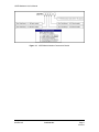
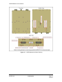
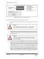
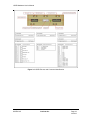
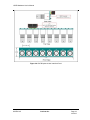
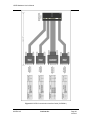
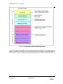
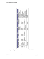
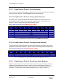
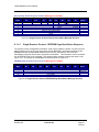
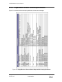
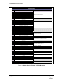
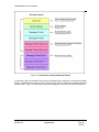
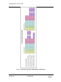
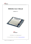
LS27B Hardware User’s Manual Dual channel Multi-Band RF Downconverter with AM and FM Demodulation Document: Author: Date: Release: U027B101 B. Graber 03/01/10 Initial Lumistar Inc 5870 El Camino Real Carlsbad, California 92008 (760) 431-2181 www.lumi-star.com This document is the intellectual property of Lumistar Inc. The document contains proprietary and confidential information. Reproduction, disclosure, or distribution of this document is prohibited without the explicit written consent of Lumistar Inc. This document is provided as is, with no warranties of any kind. Lumistar Inc disclaims and excludes all other warranties and product liability, expressed or implied, including but not limited to any implied warranties of merchantability or fitness for a particular purpose or use, liability for negligence in manufacture or shipment of product, liability for injury to persons or property, or for any incidental, consequential, punitive or exemplary damages. In no event, will Lumistar Inc, be liable for any lost revenue or profits, or other indirect, incidental and consequential damages even if Lumistar Inc has been advised of such possibilities, as a result of this document or the usage of items described within. The entire liability of Lumistar Inc shall be limited to the amount paid for this document and its contents. RESTRICTED RIGHTS LEGEND Use, duplication, or disclosure by the Government is subject to restrictions set forth in subparagraph (c)(1)(ii) of the rights in Technical Data and Computer Software clause in DFARS 252.227-7013. Lumistar Inc and its logo are trademarks of Lumistar Inc. All other brand names and product names contained in this document are trademarks, registered trademarks, or trade names of their respective holders. © 2010 Lumistar Inc. All rights reserved. Lumistar Inc 5870 El Camino Real Carlsbad, CA 92008 (760) 431-2181 (760) 431-2665 Fax www.lumi-star.com LS27B Hardware User’s Manual TABLE OF CONTENTS 1 INTRODUCTION ...................................................................................................................... 5 1.2 2 MANUAL FORMAT AND CONVENTIONS ................................................................................... 5 THEORY OF OPERATION ...................................................................................................... 9 2.1 2.2 2.3 2.4 2.5 2.6 2.7 2.8 2.9 ST 1 DOWNCONVERSION ........................................................................................................ 9 ST 1 IF BAND-PASS FILTER..................................................................................................... 9 ST 1 LOCAL OSCILLATOR........................................................................................................ 9 ND 2 DOWNCONVERSION ...................................................................................................... 10 ND 2 LOCAL OSCILLATOR ..................................................................................................... 10 ND 2 IF FILTER..................................................................................................................... 10 DIGITAL AGC/LIMITING AMPLIFICATION/AM DEMODULATION ............................................... 10 DIGITAL SIGNAL PROCESSING ENGINE (DSPE)................................................................... 10 FM DEMODULATION STAGE (OPTIONAL) ............................................................................. 10 3 INSTALLATION AND CONFIGURATION ................................................................................. 11 3.1 3.2 3.3 3.4 3.5 4 PRODUCT OUTLINE DIAGRAMS ........................................................................................... 11 HARDWARE CONFIGURATION ............................................................................................. 11 PHYSICAL INSTALLATION .................................................................................................... 15 INTERCONNECTION ............................................................................................................ 17 EXTERNAL SETUP DISCRETES ............................................................................................ 21 COMMUNICATIONS .............................................................................................................. 22 4.1 SERIAL BUS INTERFACE ..................................................................................................... 22 4.1.1 SERIAL BUS INTERFACE – DUAL RECEIVER INTERFACE PROTOCOL .................................. 22 4.1.2 SERIAL BUS INTERFACE – SINGLE RECEIVER INTERFACE PROTOCOL ............................... 22 5 COMMUNICATIONS .............................................................................................................. 23 5.1 SINGLE RECEIVER PROTOCOL............................................................................................ 23 5.1.1 SINGLE RECEIVER PROTOCOL - COMMAND AND STATUS MESSAGING ............................... 23 5.1.1.1 SINGLE RECEIVER PROTOCOL - COMMAND MESSAGING ............................................... 26 5.1.1.1.1 SINGLE RECEIVER PROTOCOL - PING COMMAND .................................................... 26 5.1.1.1.2 SINGLE RECEIVER PROTOCOL - PRIMARY SETUP COMMAND ..................................... 26 5.1.1.1.3 SINGLE RECEIVER PROTOCOL - SECONDARY SETUP COMMAND................................ 26 5.1.1.2 SINGLE RECEIVER PROTOCOL - COMMAND BIT/BYTE DEFINITIONS ............................... 27 5.1.1.3 SINGLE RECEIVER PROTOCOL - STATUS MESSAGING................................................... 30 5.1.1.3.1 SINGLE RECEIVER PROTOCOL - PRIMARY STATUS RESPONSE .................................. 30 5.1.1.3.2 SINGLE RECEIVER PROTOCOL - SECONDARY STATUS RESPONSE ............................. 30 5.1.1.4 SINGLE RECEIVER PROTOCOL - STORED SETUP STATUS RESPONSE ............................ 30 5.1.1.5 SINGLE RECEIVER PROTOCOL - EEPROM PAGE READ STATUS RESPONSE ................. 31 5.1.1.6 SINGLE RECEIVER PROTOCOL - STATUS BIT/BYTE DEFINITIONS ................................... 32 5.2 DUAL RECEIVER PROTOCOL .............................................................................................. 34 5.2.1 DUAL RECEIVER PROTOCOL - COMMAND AND STATUS MESSAGING.................................. 34 5.2.1.1 DUAL RECEIVER PROTOCOL - COMMAND MESSAGING.................................................. 37 5.2.1.1.1 DUAL RECEIVER PROTOCOL - PING COMMAND ....................................................... 37 5.2.1.1.2 DUAL RECEIVER PROTOCOL - PRIMARY SETUP COMMAND........................................ 37 5.2.1.1.3 DUAL RECEIVER PROTOCOL - SECONDARY SETUP COMMAND .................................. 37 5.2.1.2 DUAL RECEIVER PROTOCOL - COMMAND BIT/BYTE DEFINITIONS .................................. 38 5.2.1.3 DUAL RECEIVER PROTOCOL - STATUS MESSAGING...................................................... 43 5.2.1.3.1 DUAL RECEIVER PROTOCOL - PRIMARY STATUS RESPONSE ..................................... 43 5.2.1.3.2 DUAL RECEIVER PROTOCOL - EEPROM PAGE READ STATUS RESPONSE ................ 43 U027B101C Lumistar Inc. Page 3 12/19/12 LS27B Hardware User’s Manual 5.2.1.4 U027B101C DUAL RECEIVER PROTOCOL - STATUS BIT/BYTE DEFINITIONS ...................................... 46 Lumistar Inc. Page 4 12/19/12 LS27B Hardware User’s Manual 1 Introduction 1.1 General This document is the Hardware User’s Manual for the Lumistar LS27B Dual Channel Multi-band RF Downconverter. This product represents Lumistar’s 3rd generation of the LS27 Series of Dual Channel RF Downconverters. In addition to the functionalities of the Lumistar LS27P3 PCI downconverter, this product also provides and optional FM demodulation stage for each input channel. Figure 1-1 contains detailed model number construction. This document applies to all model combinations indicated by this figure. The intent of this document is to provide physical, functional, and operational information for the end user including hardware configuration, interconnection and software interfaces for the device. The design implements a Digital Signal Processor Engine (DSPE) controlled superhetrodyne downconverter with AM demodulation and optional FM demodulation. This receiver is in the physical format and size similar to a standard 5 3/4” CD or DVD drive format. The product provides two independent and autonomous multi-band downconversion stages. Each channel provides the conversion of up to four RF pass-bands to a 70MHz Intermediate Frequency (IF) output while providing AM demodulation of the input signal. The product’s standard configuration provides eight software selectable IF bandwidth filters, roughly placed at octave intervals (or as ordered by the customer), to reduce channel noise bandwidth and improve adjacent channel rejection. The product line can optionally be equipped with an FM demodulation stage and eight video filters. Table 1-1 provides specifications for electrical, mechanical, and operational characteristics of the LS27B product. A block diagram of the product design is shown in Figure 1-2. 1.2 Manual Format and Conventions This manual contains the following sections: Chapter 1 provides a brief product overview and technical specifications Chapter 2 provides receiver theory of operation Chapter 3 provides installation and configuration instructions Chapter 4 provides programming information Throughout this document, several document flags will be utilized to emphasis warnings or other important data. These flags come in three different formats: Warnings, Cautions, and Information. Examples of these flags appear below. U027B101C Lumistar Inc. Page 5 12/19/12 LS27B Hardware User’s Manual Figure 1-1 LS27B Model Number Construction Details U027B101C Lumistar Inc. Page 6 12/19/12 LS27B Hardware User’s Manual Category: Mechanical Specifications: Details: Envelope Dimensions Form Factor Weight 7.00”(L) x 5.75”(W) x 1.625” (H) 5 3/4” CD/DVD Drive Size ~ 30oz. Individual power requirements Total Power (both Channels) +12VDC @ 2A (nominal); 11-36VDC input ~ 22Watts (nominal), ~26Watts (max.) RF Input Bands 2185.5 - 2485.5 MHz (E-Band) 2200.5 - 2399.5 MHz (S-Band) 1710.5 - 1849.5 MHz (Upper L-Band) 1435.5 - 1539.5 MHz (Lower L-Band) 215.5 - 319.5 MHz (P-Band) Custom (Consult Factory) 50kHz (Typical) 0.002% (Max.) 0.001% (Typical) +10dBm to –100dBm +28dBm +10dBm (typical) 5dB (typical @ threshold) Less than -110dBc (typical) > +15dBm (typical) -20dBm (+/- 1dBm) Electrical Performance RF Tuner Demodulation Tuner Resolution Frequency Accuracy RF Input AGC Range Input Level without Damage Receiver Input P1dB Receiver Noise Figure 70MHz Phase Noise @ 100kHz Receiver OIP3 70MHz Output Level nd 2 IF 3dB Bandwidths Available (typical) Types AM -3dB Frequency Response AM Low-pass Filters AM -3dB Bandwidths FM Video Filters (typical) 250kHz, 500kHz, 1MHz, 2MHz, 5MHz, 10MHz, 20MHz, 40MHz AM, FM (optional) 50kHz (AM Low-pass Bypass Mode) 32 Software Selectable 50, 100, 200, 300, 400, 500, 600, 700, 800, 900, 1K, 1.1K, 1.2K, 1.3K, 1.4K, 1.5K, 1.6K, 1.7K, 1.8K, 1.9K, 2K, 3K, 4K, 5K, 6K, 7K, 8K, 9K, 10K, 15K, 20K, 50K Hz 125kHz, 250kHz, 500kHz, 1MHz, 2.5MHz, 4.6MHz, 10MHz, 15MHz. Connectors External Reference Input/Output RF Signal Input IF Signal Output Output Connector DC Power Connector Serial Interface, DI Connector (1) SMA Jack, Female (2) SMA Jack, Female (2) SMA Jack, Female (1) 2x8 0.100 Shrouded Header, keyed (1) 1x4 0.200 Shrouded Header, keyed (1) 2x10 0.100 Shrouded Header, keyed Environmental Temperature, Operational -40 to 85 C (Industrial) Temperature, Storage -20 to 90 C Humidity, non-condensing <40 C 0-90%, >40 C 0-75% Table 1-1 Specifications for the LS27B U027B101C Lumistar Inc. Page 7 12/19/12 LS27B Hardware User’s Manual Figure 1-2 Block Diagram of LS27B Series Multi-band Receiver U027B101C Lumistar Inc. Page 8 12/19/12 LS27B Hardware User’s Manual 2 Theory of Operation In order to more clearly understand the operation of the receiver, this section will detail the various stages of the receiver design. These stages are as follows: - st 1 Downconversion st 1 IF Band-pass Filter st 1 Local Oscillator nd 2 Downconversion nd 2 Local Oscillator nd 2 IF Filter Limiting Amplifier/AM Demodulation/Digital AGC (DAGC) Digital Signal Processing Engine (DSPE) FM Demodulation Stage (Optional) With the exception of the DSPE, each of these sections are physically shielded and isolated from one another to facilitate the greatest EMI/RFI ingress and egress protection allowing the receiver exceptional performance. For the following sections, refer to the block diagram of Figure 1-2. 2.1 1st Downconversion st The RF input is applied to the 1 Downconversion stage. The stage may optionally contain a bias-T which can be used to power an external LNA through the RF interface port. (Contact the factory for further details on this option.) A DAGC section is next in the signal chain for very high level signal protection and compression compensation. This is followed by a low-noise amplifier (LNA) to provide a large amount of gain while maintaining a very low noise figure enhancing the receiver’s overall sensitivity. Selectable RF band-pass filters follow the LNA. The RF signal is st then mixed with the first local oscillator (LO) which converted to the 1 IF frequency. 2.2 1st IF Band-pass Filter st st The output of the 1 Downconversion stage is send through one of two1 IF filter paths based on the selection of high-side or low side conversion. To eliminate images and limit the overall noise bandwidth to the remaining receiver sections, a 50MHz band-pass filter is switched into the signal path. 2.3 1st Local Oscillator In a superhetrodyne design, local oscillators (LOs) are utilized to convert high frequencies to lower, “intermediate” frequencies. The first LO is injected into the mixer of the first Downconversion stage to accomplish this task. Mixers can either utilize a sum or difference frequency component to produce IF frequencies. For example, if an RF frequency of 2,200 MHz was to be converted to an intermediate frequency of 250MHz, a difference component of 1,950MHz could injected to the mixer or a sum frequency component of 2,450MHz could be applied. The difference component LO application is referred to a “low-side” conversion. The sum component application is referred to as “high-side” conversion. Both methods are equally valid and each has its own benefits. The LS27B design has the ability to utilize either approach and actually switch between the methods when necessary for performance reasons. U027B101C Lumistar Inc. Page 9 12/19/12 LS27B Hardware User’s Manual 2.4 2nd Downconversion nd st The receiver designs contain a switchable 2 Downconversion stage. Similar to the 1 st Downconversion stage, it contains a mixer to convert the 1 IF frequency to a second IF frequency of 70MHz. If the RF frequency band is relatively low, as is the case for P-Band inputs, nd the on-board processor can bypass the 2 Downconversion stage switching to a single superhetrodyne process. In either case, a low-pass filter is applied to the signal path at the output of this stage to reduce harmonics and low frequency noise from being applied to subsequent stages. 2.5 2nd Local Oscillator nd The second LO is injected into the mixer of the 2 Downconversion stage to provide the second IF frequency of 70MHz. Like the first conversion stage, the second LO utilizes low-side injection for this conversion. A low-pass filter is applied to the LO output to minimize spurious and nd nd harmonic signals from being converted in the 2 Downconversion stage. The 2 LO is automatically disabled for RF bands that employ a single super heterodyne process. 2.6 2nd IF Filter nd From the output of the 2 conversion stage, the resulting intermediate frequency is then applied to a group of bandpass filters to minimize noise bandwidth and improve adjacent channel nd rejection. The 2 IF stage contains eight IF (SAW) filters centered at 70MHz and varying in bandwidth from 250kHz to 40MHz in approximately octave steps. 2.7 Digital AGC/Limiting Amplification/AM Demodulation nd Outputs from the 2 IF Filter Stage are routed to the final signal detection, AM demodulation, and gain stage in the receiver. The output stage combines both a limiting amplifier and digital AGC (DACG) section. Included in the design is an AM demodulation stage for antenna tracking applications. The main system gain element provides for 90 to 110dB of signal gain. Signal level detection is utilized in DAGC controls. 2.8 Digital Signal Processing Engine (DSPE) The LS27B design contains a highly integrated digital signal processing engine (DSPE) which is utilized for linearization, filtering and control applications. This engine is composed of a digital signal processor, FPGA resources, ADCs, DACs and localized memory used to process the signal path parameters. Each of the channels is controlled and statused as an autonomous receiver. The engine performs “real-time” tasks as well as user software interfaces. 2.9 FM Demodulation Stage (Optional) The LS27B design may optionally contain an FM demodulation stage for each channel. The stage is split between a narrow-band and wide-band demodulator to optimize processing of each signal characteristic. The output of the FM demodulation is software switched between one of eight video filters. The output can also be switched, in addition to the video filter, thru a video deemphasis network for true analog video signals. The unit is comes standard with NTSC deemphasis but other formats are available. The demodulation stage has a software adjustable output level. U027B101C Lumistar Inc. Page 10 12/19/12 LS27B Hardware User’s Manual 3 Installation and Configuration Chapter 3 provides installation and configuration information. This chapter will familiarize the user with the layout of the device, and provide information on the proper installation and interconnection of the hardware. 3.1 Product Outline Diagrams Figure 3-1 contains an outline diagram of the top and bottom sides of the product. Connector locations and switch positions are indicated. The model number, serial number, revision information and product options are denoted on the RF enclosure label. 3.2 Hardware Configuration The receiver design contains configuration switches to control various functions. Figure 3-2 contains a diagram of the configuration switches along with the default factory positions for these switches. U027B101C Lumistar Inc. Page 11 12/19/12 LS27B Hardware User’s Manual Figure 3-1 LS27B Mechanical Outline Drawing U027B101C Lumistar Inc. Page 12 12/19/12 LS27B Hardware User’s Manual Figure 3-2 Receiver Configuration Switch SW1 The configuration switches in Figure 3-2 have the following functions: 1.) The SW1-1 is defined as FACTORY USE and should remain in the OFF state as shown. 2.) The SW1-2 switch sets the LS27B to SW Development mode. When the switch is in the ON position, the serial status messages will contain dynamic data. The intent of this switch is to aid the development of user software without the necessity of having any inputs to the unit. 3.) J2 allows for either an external reference source to be supplied to the receiver for synchronization to external RF hardware, or for the output of an on-board 10MHz reference to synchronize other external items to the unit’s synthesizer reference source. SW1-3 controls the operation of the synthesizer reference clock distribution and PLL at boot-time. When SW1-3 is in the OFF position, the J2 connection is in an automatic sense mode. In this mode, at boot-time, the clock distribution system monitors for the presence of an external reference at port J2 (see Figures 3-1). If there is no external reference present at J2 (10MHz @ +4dBm) within 250msecs of boot-time, the unit will automatically switch the J2 input port to an output mode, enable on on-board 10MHz TCXO (+/- 3ppm stability minimum), and the route the 10MHz TCXO source to both the J2 output (at +2 to -2dBm @ 50 ohms) and use it to U027B101C Lumistar Inc. Page 13 12/19/12 LS27B Hardware User’s Manual synchronize the internal synthesizers. When SW1-3 is in the ON position, the internal LS27B 10MHz reference clock will be disabled and the J2 connector will be switched to be a dedicated input. In this mode, the unit will presume the presence of an external 10MHz reference source. 4.) Switch SW1-5 initiates the serial override mode. When in the ON position, the serial interface is automatically set to 57.6K BAUD for each serial communications channel. When in the OFF position, commands to alter the serial data rate can be issued. 5.) Switches SW1-7 and SW1-8 define the LS27B power-up boot configuration selection. This combination of switches allows the user to select pre-stored configuration setups by various methods. The description of these methods follows: a. NULL Boot Mode – In this mode, the LS27B receivers will not tune to any stored setups that may have been previously stored in the unit’s internal nonvolatile memory. When commanded via one of the appropriate serial interfaces, it will tune the receiver as commanded. In this mode, storage of setup parameters are stored in internal non-volatile memory. b. Discrete Boot Mode – In this mode, the LS27B receiver will be setups will be selected via the state of the external discrete lines on P3-7 thru P3-10. These discrete lines will determine a four bit number from zero to fifteen. At boot time, the LS27B will tune both receivers to the setup whose number is defined by the values of the discrete lines. Note that each receiver may still be tuned to a different frequency and setup, since each receiver has a separate list of 16 setups. Subsequent serial setup commands will override the boot setup and save that setup in non-volatile memory. c. Boot Last Mode – In this mode LS27B will program the receivers with the last valid setup. Subsequent setup commands will override the boot setup and replace the setup as directed by the user. d. Boot Prohibit Mode - This mode is designed for security conscious requirements. In this state the LS27B will not tune to any setup at power-up. Any serial commands will setup the receivers as usual, but no information will be retained internally in non-volatile memory. In addition, at boot time any existing setup information in any of the sixteen possible setup locations in non-volatile memory will be deleted. 6.) Switches defined as “Undefined/Future” have no implementation and thus their state is irrelevant. U027B101C Lumistar Inc. Page 14 12/19/12 LS27B Hardware User’s Manual 3.3 Physical Installation To install the receiver in the target computer system, the following procedure should be followed: 1. Perform a normal system shutdown of the target host system and remove the primary power plug. 2. Install the receiver in an unobstructed DVD/CD drive bay or in mounting rails. PCs vary in their mechanical configurations so it may be necessary to remove additional PC hardware to properly install the unit. 3. For mounting hardware locations, reference the Specification Control Drawing for the product (Doc. Number: M27B0101). 4. It is recommended that at least four 4-40UNC mounting screws (provided) be used in the mounting of the unit. This accommodates higher vibration and shock environments. Ensure that the installation provides room for the RF and I/O connections. 5. Airflow across the unit is strongly recommended to prevent long-term heat related damage. Multiple sets of mounting holes have been provided to allow for some rear fan clearances. 6. Connect the serial control interface to an available RS/EIA-232 interface via the P3 connector. 7. Connect the user I/O as desired via the P1 connector (refer to Figure 3-3). 8. Connect the required RF and IF connections via the J-numbered connectors (refer to Figure 3-3). 9. Re-apply power to the unit and initiate the user software to communicate via the serial interface. U027B101C Lumistar Inc. Page 15 12/19/12 LS27B Hardware User’s Manual 3.4 Interconnection The receiver platforms provide multiple interface connectors. Figure 3-3 provides interface pin-outs and mating connector information for all connectors. Lumistar can provide an optional BNC style interface panel as shown in Figure 3-4 to ease the facilitation of user interfaces. Consult the factory for further details. A communication harness is provided with the delivered unit. This harness is shown in Figure 3-5. U027B101C Lumistar Inc. Page 17 12/19/12 LS27B Hardware User’s Manual Figure 3-3 LS27B Pin-outs and Connector Identification U027B101C Lumistar Inc. Page 18 12/19/12 LS27B Hardware User’s Manual Figure 3-4 LS27B Optional User Interface Panel U027B101C Lumistar Inc. Page 19 12/19/12 LS27B Hardware User’s Manual Figure 3-5 LS27B Communication Interface Cable (C27B0001) U027B101C Lumistar Inc. Page 20 12/19/12 LS27B Hardware User’s Manual 3.5 External Setup Discretes As shown in Figure 3-3, connector P3 contains five discrete selection inputs (four of which are active). These bits are used to select previously stored user setups for the LS27B without the use of a serial host interface. Each of the LS27B input channels allows the storage of up to sixteen (16) receiver setups. Using the serial interface, the user can program particular configurations for the receiver channels, and then select a corresponding storage number. The operation of these discretes is based on the boot-time mode selection switches of SW1-7 and SW1-8. (Refer to section 3.2 for the proper setting of the configuration switches to enable the use of the external setup discretes.) The discrete inputs will function as the main controls until serial communications to the unit takes place. At that point, the discrete interfaces are ignored and control of the unit is switched to the serial interface. Selection of the discrete (logic 1) is made by connecting the desired discrete input to P3-13 pin. If the discrete input is left disconnected, the input will be considered logic 0. DIO 4-0 Setting 0000b 0001b 0010b 0011b 0100b 0101b 0110b 0111b 1000b 1001b 1010b 1011b 1100b 1101b 1110b 1111b Format Selected Programmed Setup 0 Programmed Setup 1 Programmed Setup 2 Programmed Setup 3 Programmed Setup 4 Programmed Setup 5 Programmed Setup 6 Programmed Setup 7 Programmed Setup 8 Programmed Setup 9 Programmed Setup 10 Programmed Setup 11 Programmed Setup 12 Programmed Setup 13 Programmed Setup 14 Programmed Setup 15 Table 3-1 LS27B External Discrete Setup Selection Table U027B101C Lumistar Inc. Page 21 12/19/12 LS27B Hardware User’s Manual 4 Communications This chapter provides communications interface information pertaining to the LS27B drive bay dual receiver. 4.1 Serial Bus Interface The LS27B is controlled and statused via a standard RS/EIA-232 asynchronous, 3-wire, serial interface method. The interface is capable of being run at rates between 9.6k BAUD and 115.2k BAUD with a default rate of 57.6k BAUD. The unit is shipped with SW1-5 position in the ON position. In this position, the unit will only communicate at 57.6k BAUD. (See programming section for details on how to alter the serial communication BAUD rate.) The host communication channel should be setup in the following configuration: Number of bits: 8 Parity: None Stop Bits: 1 Flow Control: None The design contains three serial interface channels, operating via two different protocols: “single receiver protocol” and “dual receiver protocol”. Refer to Figure 3-3 for pin-out assignments. 4.1.1 Serial Bus Interface – Dual Receiver Interface Protocol The Serial “A” bus, contained on P3 pins 1 thru 3, communicates via the “Dual Receiver Interface Protocol” defined in chapter 5. This protocol is “enhanced” from the existing “LS25B” protocol and provides for controls for both receiver channels via a single physical interface. 4.1.2 Serial Bus Interface – Single Receiver Interface Protocol The Serial “B” bus, contained on P3 pins 14 thru 16, and Serial “C” bus, contained on P3 pins 18 thru 20, communicates via the existing LS25B Single Receiver Interface Protocol defined in chapter 5. The Serial “B” control/status interface is dedicated to the Channel 1 receiver. The Serial “C” bus control/status interface is dedicated to Channel 2 receiver. U027B101C Lumistar Inc. Page 22 12/19/12 LS27B Hardware User’s Manual 5 Communications This chapter provides interface protocol information for the LS27B drive bay dual receiver. The LS27B product provides a dual protocol interface method. It supports a “single receiver protocol” which is operational compatible with the previous Lumistar generation of LS25B drive-bay receiver. It also supports an enhanced “dual receiver protocol” which provides some additional functional capabilities. 5.1 Single Receiver Protocol Single receiver protocol is active on serial interface B which controls receiver number one of the device, and serial interface C, which controls receiver number two. The two receiver interfaces can be operated simultaneously and autonomously. All command/status information contained in the following sections relates to single channel operation but the format is identical between channels. 5.1.1 Single Receiver Protocol - Command and Status Messaging Interface using the single receiver protocol is via command-response messaging. For every command sent from the host, the receiver will respond to indicate that the command was received. Commands from the host are grouped in two categories: primary commands and secondary commands. Primary commands are used to control the basic tuning and setup of the receiver. Secondary commands are used to set various “lower-priority” operational modes and to obtain secondary status. Secondary host commands occasionally require that the host send two commands: a first command followed by a status request message. All host messages require a message header of six (6) bytes. If the host command requires additional data be transferred to the host, the data will immediately follow the command header. Figure 5-1 contains a diagram of the message header for the single receiver protocol. The first byte of the message header contains a device identification flag of 0x25. The second byte indicates the module address being commanded. For RS-232 communications, this should always be set to 0x00. Bytes 3 and 4 contain the message identification. Message identification informs the type and format of data that will follow the header, if any. Bytes 5 and 6 of the message header indicate the number of command related bytes that follow the message header. U027B101C Lumistar Inc. Page 23 12/19/12 LS27B Hardware User’s Manual Figure 5-1 Single Receiver Protocol Message Format In response to any host command, the protocol will respond with a minimum of an echoed message header. If additional information is to be conveyed to the host, the data will immediately follow the echoed header. Figure 5-2 indicates the general configuration of the host and terminal responses. U027B101C Lumistar Inc. Page 24 12/19/12 LS27B Hardware User’s Manual Figure 5-2 Single Receiver Protocol Messaging Configurations U027B101C Lumistar Inc. Page 25 12/19/12 LS27B Hardware User’s Manual 5.1.1.1 Single Receiver Protocol - Command Messaging There are three command message types: a “Ping” command, a “Primary Setup” command, and a “Secondary Setup” command. 5.1.1.1.1 Single Receiver Protocol - PING Command The “Ping” command is used as to determine the health/presence of the communications channel between the host and the receiver. In response to the “Ping” command, the receiver will echo the received message header back to the host. 5.1.1.1.2 Single Receiver Protocol - Primary Setup Command The “Primary Setup” command is provides fundamental control information to the receiver channel. The message header is followed by eight (8) data bytes as defined in Figure 5-3. Primary Command Message Content (Message ID = 0x1000) Content Byte D7 D6 D5 D4 D3 1 2 3 4 5 6 7 8 TLM2DEMP DO3 POLARITY DO2 VFILT - AMINV DO1 REF DO0 - - - D2 D1 D0 Notes: LINEAR TCONST IFFILT AMFILT RFBAND TUNE1 (Fc /256MHz) TUNE2 (Fc mod 256MHz/1MHz) TUNE3 (Fc mod 1MHz/10kHz) SNUM Figure 5-3 Single Receiver Protocol Primary Message Command Structure 5.1.1.1.3 Single Receiver Protocol - Secondary Setup Command The “Secondary Setup” command is provides non-critical control information to the receiver channel and requests that internal status from the controlled channel. The message header is followed by six (6) data bytes as defined in Figure 5-4. U027B101C Lumistar Inc. Page 26 12/19/12 LS27B Hardware User’s Manual Secondary Command Message Content (Message ID = 0x1001) Content Byte D7 1 2 3 4 5 6 D6 D5 D4 D3 D2 D1 D0 Notes: MODE CMD1 CMD2 CMD3 CMD4 CMD5 Figure 5-4 Single Receiver Protocol Secondary Message Command Structure 5.1.1.2 Single Receiver Protocol - Command Bit/Byte Definitions Figure 5-5 contains the bit and bit pairing definitions for the primary and the secondary messages. Figure 5-6 contains the definition for the secondary message mode byte. U027B101C Lumistar Inc. Page 27 12/19/12 LS27B Hardware User’s Manual Figure 5-5 Single Receiver Protocol Command Bit Grouping Definitions U027B101C Lumistar Inc. Page 28 12/19/12 LS27B Hardware User’s Manual Figure 5-6 Single Receiver Protocol Secondary Command Mode Definitions U027B101C Lumistar Inc. Page 29 12/19/12 LS27B Hardware User’s Manual 5.1.1.3 Single Receiver Protocol - Status Messaging There are four (4) status message types: primary status response, secondary status response, stored setup status response, and the EEPROM Page read status response. 5.1.1.3.1 Single Receiver Protocol - Primary Status Response The primary status response provides the host with fundamental receiver status such as the received signal strength, FM deviation measurement, AM index value, and the detected AM frequency. Figure 5-7 depicts the primary status message content. Primary Status Response Content (Message ID = 0x2000) Content Byte 1 2 3 4 5 6 7 8 D7 D6 D5 D4 RSSI7 - RSSII6 - RSSI5 - RSSI4 - D3 RSSI3 - D2 D1 MODID RSSI2 RSSI1 RSSI9 D0 Notes: RSSI0 RSSI8 DEV AMI AMFREQ1 AMFREQ2 SNUM Figure 5-7 Single Receiver Protocol Primary Status Message Structure 5.1.1.3.2 Single Receiver Protocol - Secondary Status Response The secondary status response provides the receiver with configuration information and provides information relates to mode commands. Figure 5-8 depicts the secondary status message content. Secondary Status Response Content (Message ID = 0x2001) Content Byte D7 1 2 3 D6 D5 D4 D3 D2 D1 D0 Notes: MODE RTN1 RTN2 Figure 5-8 Single Receiver Protocol Secondary Status Message Structure 5.1.1.4 Single Receiver Protocol - Stored Setup Status Response A total of sixteen (16) receiver setups can be stored in the receiver’s internal memory and then be recalled by simply providing an index value. (Future provisions will allow these setups to be activated via discrete interaction.) These configurations can be reviewed using secondary mode commands. The stored setup status response message structure is shown in Figure 5-9. U027B101C Lumistar Inc. Page 30 12/19/12 LS27B Hardware User’s Manual Stored Setup Status Response Content (Message ID = 0x2002) Content Byte 1 2 3 4 5 6 7 8 D7 D6 D5 D4 D3 TLM2DEMP - POLARITY VFILT - AMINV - REF - - - - D2 D1 D0 Notes: LINEAR TCONST MODID IFFILT AMFILT RFBAND TUNE1 (Fc /256MHz) TUNE2 (Fc mod 256MHz/1MHz) TUNE3 (Fc mod 1MHz/10kHz) SNUM Figure 5-9 Single Receiver Protocol Stored Setup Status Message Structure 5.1.1.5 Single Receiver Protocol - EEPROM Page Read Status Response The primary receiver configuration information, used to drive software controls, is found in the first page (indexed from 0) of the receivers primary internal EEPROM. Information contained in this EEPROM includes the bandwidths installed in the receiver, associated IF and video filter bandwidths, along with various other configuration information. This information can be accessed via an EEPROM read mode command. The resulting status message contents are shown in the Figure 5-10. An example of the EEPROM contents is shown in Figure 5-12. EEPROM Page Read Response Content (Message ID = 0x2009) Content Byte 1 2 … 127 128 D7 D6 D5 D4 D3 LOC0_LSB LOC0_MSB … LOC63_LSB LOC63_MSB D2 D1 D0 Notes: More bytes Figure 5-10 Single Receiver Protocol EEPROM Page Read Status Message Structure U027B101C Lumistar Inc. Page 31 12/19/12 LS27B Hardware User’s Manual 5.1.1.6 Single Receiver Protocol - Status Bit/Byte Definitions Figure 5-11 contains the bit and bit pairing definitions for the status messages. Figure 5-11 Single Receiver Protocol Status Response Bit Grouping Definitions U027B101C Lumistar Inc. Page 32 12/19/12 LS27B Hardware User’s Manual EEPROM Map Offset Contents 0 1 Signal Bandwidth IF Filter 0 (kHz) Signal Bandwidth IF Filter 1 (kHz) 2 Signal Bandwidth IF Filter 2 (kHz) 3 4 Signal Bandwidth IF Filter 3 (kHz) Signal Bandwidth IF Filter 4 (kHz) 5 6 Signal Bandwidth IF Filter 5 (kHz) Signal Bandwidth IF Filter 6 (kHz) 7 8 Signal Bandwidth IF Filter 7 (kHz) (Unused / Spare) 9 10 (Unused / Spare) (Unused / Spare) Description/ Information IF Filter Bandwidth (Hz) = Value x1000 Hz 11 (Unused / Spare) 12 13 Signal Bandwidth Video Filter 0 (kHz) Signal Bandwidth Video Filter 1 (kHz) 14 15 Signal Bandwidth Video Filter 2 (kHz) Signal Bandwidth Video Filter 3 (kHz) 16 17 Signal Bandwidth Video Filter 4 (kHz) Signal Bandwidth Video Filter 5 (kHz) 18 Signal Bandwidth Video Filter 6 (kHz) 19 20 Signal Bandwidth Video Filter 7 (kHz) (Unused / Spare) 21 22 (Unused / Spare) (Unused / Spare) 23 24 (Unused / Spare) RF Input Attenuator Set Point 25 26 (Unused / Spare) RF Band 0 Start Frequency (MHz) 27 RF Band 0 Stop Frequency (MHz) 28 29 RF Band 1 Start Frequency (MHz) RF Band 1 Stop Frequency (MHz) 30 31 RF Band 0 Linear Output Compression RF Band 1 Linear Output Compression 32 33 AGC Time Constant Count #0 AGC Time Constant Count #1 34 AGC Time Constant Count #2 35 36 AGC Time Constant Count #3 (Unused / Spare) 37 38 (Unused / Spare) AM LPF Filter #0 39 40 AM LPF Filter #1 AM LPF Filter #2 41 42 AM LPF Filter #3 De-emphasis Filter Line Count 43 (Unused / Spare) 44 45 Max Preset Value Active Setup Value Video Filter Bandwidth (Hz) = Value x1000 Hz RF Band Edge = Value x 1MHz Linear Output Compression Point (RSSI Count) AGC Time Constant (msec) = Constant Count x 0.1msec AM Low-pass filter Bandwidth = Value x 1Hz Video Line Count: 525 = NTSC Maximum number of User Presets (Indexed from 0) Preset Number at Boot-time 46 47 (Unused / Spare) (Unused / Spare) 48 49 FPGA Firmware ID DSP Firmware ID1 FPGA Firmware Number DSP Firmware Date: MSB = Month in Hex, LSB = Day in Hex 50 DSP Firmware ID2 DSP Firmware Date: Two Bytes = Year in Hex 51 52 Board Serial Number MSW Board Serial Number LSW 53 54 Primary Configuration ID Options #1 55 56 57 Options #2 (Unused / Spare) Serial Channel Baud Rate 58 59 Serial Channel Format (Unused / Spare) 60 (Unused / Spare) 61 62 Ext. Ref. Input Freq. Multiplier (Unused / Spare) 63 (Unused / Spare) Device Serial Number in Hex. ASCII Representation Of Device ID (Always 0x25) ASCII Representation Of Device Options (Future Use) Serial Channel BAUD/100 Serial Channel Signaling Level = 232 External Reference Input Frequency = Multiplier x 1MHz Figure 5-12 Single Receiver Protocol - EEPROM Contents U027B101C Lumistar Inc. Page 33 12/19/12 LS27B Hardware User’s Manual 5.2 Dual Receiver Protocol Dual receiver protocol is active on serial interface A only. This interface controls both internal receivers using the same serial interface channel. Each receivers operations are autonomous. 5.2.1 Dual Receiver Protocol - Command and Status Messaging Interface using the dual receiver protocol is via command-response messaging. For every command sent from the host, the receiver will respond to indicate that the command was received. Commands from the host are grouped in two categories: primary commands and secondary commands. Primary commands are used to control the basic tuning and setup of the receiver. Secondary commands are used to set various “lower-priority” operational modes and to obtain secondary status. Secondary host commands occasionally require that the host send two commands: a first command followed by a status request message. All host messages require a message header of six (6) bytes. If the host command requires additional data be transferred to the host, the data will immediately follow the command header. Figure 5-13 contains a diagram of the message header for the dual receiver protocol. The first byte of the message header contains a device identification flag of 0x27. The second byte indicates the module address being commanded which should always be set to 0x00. Bytes 3 and 4 contain the message identification. Message identification informs the type and format of data that will follow the header, if any. Bytes 5 and 6 of the message header indicate the number of command related bytes that follow the message header. U027B101C Lumistar Inc. Page 34 12/19/12 LS27B Hardware User’s Manual Figure 5-13 Dual Receiver Protocol Message Format In response to any host command, the protocol will respond with a minimum of an echoed message header. If additional information is to be conveyed to the host, the data will immediately follow the echoed header. Figure 5-14 indicates the general configuration of the host and terminal responses. U027B101C Lumistar Inc. Page 35 12/19/12 LS27B Hardware User’s Manual Figure 5-14 Dual Receiver Protocol Messaging Configurations U027B101C Lumistar Inc. Page 36 12/19/12 LS27B Hardware User’s Manual 5.2.1.1 Dual Receiver Protocol - Command Messaging There are four command message types: a “Ping” command, a “Primary Setup” command, a “Secondary Setup” command, and a “Append Flash File Section” command. 5.2.1.1.1 Dual Receiver Protocol - PING Command The “Ping” command is used as to determine the health/presence of the communications channel between the host and the receiver. In response to the “Ping” command, the receiver will echo the received message header back to the host. 5.2.1.1.2 Dual Receiver Protocol - Primary Setup Command The “Primary Setup” command is provides fundamental control information to the receiver channel. The message header is followed by eight (8) data bytes as defined in Figure 5-3. Primary Command Message Content (Message ID = 0x1000) Content Byte D7 D6 D5 D4 1 2 3 4 5 6 7 8 INTREF LIM AMINV - POLARITY - - D3 D2 SNUM FRZ IFBW DEMP AMFIL TUNE1 (Fc /256MHz) TUNE2 (Fc mod 256MHz/1MHz) TUNE3 (Fc mod 1MHz/10kHz) D1 AGCTC VFILT D0 Notes: CHx - Figure 5-15 Dual Receiver Primary Protocol Message Command Structure 5.2.1.1.3 Dual Receiver Protocol - Secondary Setup Command The “Secondary Setup” command is provides control information to the receiver channel commanded and requests that internal status from the controlled channel. The message header is followed by four (4) data bytes as defined in Figure 5-15. Secondary Command Message Content (Message ID = 0x1001) Content Byte D7 1 2 3 4 D6 D5 D4 D3 MODE D2 D1 D0 - - CHx Notes: CMD1 CMD2 CMD3 Figure 5-15 Dual Receiver Protocol Secondary Message Command Structure U027B101C Lumistar Inc. Page 37 12/19/12 LS27B Hardware User’s Manual 5.2.1.1.4 Dual Receiver Protocol – Append Flash File Section Command This command can be used to program the DSP with a successor flash file. This process is analogous to updating the BIOS on a personal computer. Contact Lumistar, Inc. for further information and to receive the latest DSP flash file. The DSP flash file can be divided into 128 byte sections and loaded into the DSP’s onboard memory with multiple 0x1020 commands. The last 0x1020 command may have a body less than 128 bytes long to accommodate the different possible lengths of the DSP flash file. In that case, the “Bytes to Follow” value in the command header section should be set to the actual number of bytes in the command body. After the last flash file section has been delivered to the DSP, send a 0x1001 Secondary Setup command with a 0x13 value in the Mode field and a 0xFF value in the CMD1 field. When the DSP receives this command it will use the reconstructed flash file that it has retained in local memory and write this file into the flash RAM. Depending on the current DSP flash file version, it may load the file and then begin blinking the LED at about 1 Hz. The LS27B will then need to be power cycled before any further commands are sent to it. More recent DSP versions will reboot after the successor file has been fully written to DSP flash RAM. 5.2.1.2 Dual Receiver Protocol - Command Bit/Byte Definitions Figure 5-16 contains the bit and bit pairing definitions for the primary and the secondary messages. Figure 5-17 contains the definition for the secondary message mode byte. Figure 5-18 contains the definitions for the secondary message mode responses. U027B101C Lumistar Inc. Page 38 12/19/12 LS27B Hardware User’s Manual Figure 5-16 Dual Receiver Protocol Command Bit Grouping Definitions U027B101C Lumistar Inc. Page 39 12/19/12 LS27B Hardware User’s Manual Mode Definition EEPROM Mode 0x02 0x03 Tune Mode DAGC Control Mode 0x04 0x06 0x07 0x08 0x09 0x0A Read AM LPF Table Read AM Freq Value Program Ext Ref Freq Read SW2 Mode Cmd Program Custom Time Constants Select AGC Out Range CMD1 EEPROM Sub Mode: 000pppppb = PROM Page No. 01aaaaaab = RD Offset Pg Address (LSB is returned on STAT2, MSB is returned on STAT3). Fc Mod 1MHz/10Khz 0x00 = LINEAR 0x01 = LIMITED 0x02 = COMBINER (Not implemented) 0x03 = RESERVED (Not implemented) (Unused) (Unused) (Unused) (Unused) Custom Time Constant Number (Values between 1 and 3) (Unused) 0x0B Program Digipot Mode 0x0D 0x0E 0x0F 0x10 Programmable AGC Out dBm Range Programmable AGC Out Voltage Range DAC Adjust Mode Get Setup Info Mode 0x12 0x13 DSP Flash Update Mode External Values Mode 0x14 RSSI Averaging Mode 0x17 0x1F Serial Channel Control Mode Digipot Instruction: 0x01 = Decrement Digipot 0x02 = Increment Digipot 0x03 = Set Digipot to Preset Value 0x04 = Query Digipot Setting 0x05 = Set Digipot to Default Value Lower dBm value in 2’s complement format. Valid range is from -110 to 10. Granularity is 1 dBm. Starting voltage value * 10 in 2’s complement format. Valid range is from 40 (4.0 V) to -40 (-4.0 V). Granularity is 0.1 V. DAC Selection: 0x01 = Video Output Adjust 0x00 = Get DCxCTRL124 Submode. 0x01 = Get Tune Freq Submode. 0x02 = Get DAGC Values Submode. 0x03 = Get AGC Out dBm Range. 0x04 = Get AGC Out Voltage Range. 0x05 = Get Miscellaneous Values. DSP Flash Update SubMode: 0x00 = Append Flash Value 0xFF = Write Stored Values External Values Submode: 0x00 = RSSI Correction Submode. 0x01 = Compression Point Submode. RSSI Averaging Submode. 0x00 = Set Number of RSSI Samples. 0x01 = Set RSSI Averaging Function. 0x02 = Enter AFRZ Mode. 0x03 = Exit AFRZ Mode. 0x00 = Serial Baudrate Select Submode. CMD2 CMD3 (Unused) (Unused) (Unused) (Unused) Fc MOD 256MHz/1MHz Fc/256MHz (Unused) (Unused) Table Index (0 to 31) (Unused) Allowable: 5, 10, 20, 25 MHz (Unused) 8 LSBs of 100uSec TConstant Multiple (Unused) (Unused) (Unused) (Unused) 8 MSBs of 100uSec TConstant Multiple (Unused) 0x00 = -4V to 0V, 0x08 = 0V to -4V, 0x01 = -2V to 0V, 0x09 = 0V to -2V, 0x02 = 0V to +2V, 0x0A = 2V to 0V, 0x03 = 0V to +4V, 0x0B = 4V to 0V, 0x04 = -2V to +2V, 0x0C = 2V to -2V, 0x05 = -4V to +4V, 0x0D = 4V to -4V, All others undefined. Digipot Select: 0x00 = AM Gain Digipot Preset Value: 0-99 Upper dBm value in 2’s complement format. Valid range is from -110 to 10. Granularity is 1 dBm. Ending voltage value * 10 in 2’s complement format. Valid range is from 40 (4.0 V) to -40 (-4.0 V). Granularity is 0.1 V. 8 LSBs of DAC Setting (Unused) (Unused) (Unused) LSB of Flash Value Word (Unused) MSB of Flash Value Word (Unused) RSSI Correction MSB Compression Point MSB RSSI Correction LSB Compression Point MSB Value from 2 to 50. 0=Simple Average, 1=Filtered Average. (Unused) (Unused) 8 LSBits of (BAUD Rate/100). (Unused) (Unused) (Unused) (Unused) (Unused) 6 MSBs of DAC Setting 3 MSBits of (BAUD Rate/100). Figure 5-17 Dual Receiver Protocol Secondary Command Mode Definitions U027B101C Lumistar Inc. Page 40 12/19/12 LS27B Hardware User’s Manual Mode 0x02 0x02 0x03 0x04 0x06 0x07 0x08 Functional Mode STAT2 Page Offset 8 LSBs of EEPROM Read Value EEPROM Mode: Pg Set Tune Mode DAGC Control Mode Read AM LPF Table Page Number Fc Mod 1MHz/10Khz DAGC Control Mode Commanded Index Value (Unused = 0) Fc MOD 256MHz/1MHz (Unused = 0) 8 LSBs of AM LPF Fc Frequency Read AM Freq Counter 8 LSBs of AM Counter Frequency 8 Mid-SBs of AM Counter Frequency Program Ext Ref Freq (Unused = 0) Read SW2 0x00=LS27B 0x80=LS27P3 Ext Ref Frequency in MHz (5,10,20,25) LS27B: SW2 Values (0x00 to 0xFF) LS27P3: SW2 Values (0x00 to 0x0F) Program Custom Time Constants Custom Time Constant Number (Values between 1 and 3) (Unused = 0) 0x09 0x0A STAT1 EEPROM Mode: Read Select AGC Output Range If Submode=0x00, STAT1=0 If Submode=0xFF DSP will reboot. 0x00 = -4V to 0V, 0x08 = 0V to -4V, 0x01 = -2V to 0V, 0x09 = 0V to -2V, 0x02 = 0V to +2V, 0x0A = 2V to 0V, 0x03 = 0V to +4V, 0x0B = 4V to 0V, 0x04 = -2V to +2V, 0x0C = 2V to -2V, 0x05 = -4V to +4V, 0x0D = 4V to -4V, All others undefined. Current Digipot Setting (0 – 99) Upper dBm value in 2’s complement format. Ending voltage value * 10 in 2’s complement format. 8 LSBs of the DAC Setting |7|6|5|4| 3 |2| 1 | 0 | |-| IFBW|DEEMP|-|BANDOFPREF| Fc MOD 256MHz/1MHz DAGC Time Const in μsec MSB Upper dBm value in 2’s comp format End voltage * 10 in 2’s comp format Number of RSSI Samples MSB External RSSI Correction LSB External Compression Point LSB If Submode=0x00, STAT2=0 If Submode=0xFF DSP will reboot. (Unused = 0) (Unused = 0) (Unused = 0) (Unused = 0) 0x0B 0x0D 0x0E 0x0F 0x10 0x12 Program Digipot Mode Programmable AGC Out dBm Range Programmable AGC Out Voltage Range DAC Adjust Mode Get Setup Info Submodes: 0x00=Get DCxCTRL124 Submode. 0x01=Get Tune Freq Submode. 0x02=Get DAGC Values Submode. 0x03=Get AGC Out dBm Range. 0x04=Get AGC Out Voltage Range. 0x05=Get Miscellaneous Values. 0x06=Get External RSSI Correction 0x07=Get External Compression Pt. DSP Flash Update Mode 0x13 0x14 0x1F External Values Mode Serial Channel Control Mode 8 LSBs of 100 μsec Tconstant Multiple Lower dBm value in 2’s complement format. Starting voltage value * 10 in 2’s complement value. DAC Selection Value | 7 | 6 |5|4| 3 |2|1| 0 | | LIM|AGCZERO|-|-|FRZ|-|-| - | Fc Mod 1MHz/10Khz DAGC Time Const in μsec LSB Lower dBm value in 2’s comp format Start voltage value * 10 in 2’s comp |AFRZ|RSSIAVEFUNC| VFIL |CAL| External RSSI Correction MSB External Compression Point MSB STAT3 8 MSBs of EEPROM Read Value (Unused = 0) Fc/256MHz (Unused = 0) 8 MSBs of AM LPF Fc Frequency 1 MSB of AM Counter Frequency (Unused = 0) LS27B3 Ext. Disc. Lines (0x00-0x1F) LS27P3: Unused, 0x00 8 MSBs of 100 μsec Tconstant Multiple (Unused = 0) (Unused = 0) (Unused = 0) 6 MSBs of the DAC Setting | 7 |6|5|4|3|2|1|0| |AMINV|-|-| AMFLT | Fc/256MHz DAGC Control Mode (Unused = 0) (Unused = 0) Number of RSSI Samples LSB (Unused = 0) (Unused = 0) If Submode=0x00, STAT3=0 If Submode=0xFF DSP will reboot. (Unused = 0) (Unused = 0) Figure 5-18 Dual Receiver Protocol Secondary Command Mode Responses U027B101C Lumistar Inc. Page 41 12/19/12 LS27B Hardware User’s Manual Get DCxCTRL124 Submode=0x00 STAT1 STAT2 STAT3 Get Tune Frequency Submode=0x01 STAT1 STAT2 STAT3 Get Ext. RSSI Correction Submode=0x06 6 5 7 6 5 STAT1 STAT2 STAT3 3 2 AMFIL 4 3 Fc Mod 1MHz/10Khz Fc MOD 256MHz/1MHz Fc/256MHz 4 1 0 - 3 BANDOFPREF 2 1 0 2 1 0 AGCTC LSB AGCTC MSB DAGC CTRL MODE 7 6 5 4 3 Lower dBm Value Upper dBm Value - 2 1 0 7 6 5 4 3 Lower Voltage Value (x10) Upper Voltage Value (x10) - 2 1 0 7 AFRZ 6 2 VFIL 1 7 6 5 4 3 External RSSI Correction MSB External RSSI Correction LSB - 2 1 0 7 6 5 4 3 External Compression Point MSB External Compression Point LSB - 2 1 0 5 4 3 RSSI Averaging Function Number of RSSI Samples MSB Number of RSSI Samples LSB STAT1 STAT2 STAT3 Get External Comp. Pt. Submode=0x07 7 STAT1 STAT2 STAT3 Get Misc. Values Submode=0x05 IFBW 4 FRZ (DEEMP) - STAT1 STAT2 STAT3 Get AGC Out Volt Rng. Submode=0x04 5 - STAT1 STAT2 STAT3 Get AGC Out dBm Rng. Submode=0x03 6 AGCZERO STAT1 STAT2 STAT3 Get DAGC Values Submode=0x02 7 LIM AMINV 0 DAGC Cal Mode Figure 5-19 Dual Receiver Protocol Get Setup Info Mode Table U027B101C Lumistar Inc. Page 42 12/19/12 LS27B Hardware User’s Manual 5.2.1.3 Dual Receiver Protocol - Status Messaging There are two (2) status message types: primary status response, and the EEPROM Page read status response. 5.2.1.3.1 Dual Receiver Protocol - Primary Status Response The primary status response provides the host with fundamental receiver status such as the received signal strength, FM deviation measurement, AM index value, and the detected AM frequency. Figure 5-20 depicts the primary status message content. Primary Status Response Content (Message ID = 0x2000) Content Byte 1 2 3 4 5 6 7 8 9 D7 D6 D5 REF PLL - D4 CH1COMP - - CH1LO2 CH2COMP - - CH2LO2 D3 CH1RSSIL CH1LO1 CH1AMINDX CH1FMDEV CH2RSSIL CH2LO1 CH2AMINDX CH2FMDEV D2 D1 D0 - - - Notes: CH1RSSIH CH2RSSIH Figure 5-20 Dual Receiver Protocol Primary Status Message Structure 5.2.1.3.2 Dual Receiver Protocol - EEPROM Page Read Status Response The primary receiver configuration information, used to drive software controls, is found in the first page (indexed from 0) of the receivers primary internal EEPROM. Information contained in this EEPROM includes the bandwidths installed in the receiver, associated IF and video filter bandwidths, along with various other configuration information. This information can be accessed via an EEPROM read mode command. The EEPROM read status command structure is shown in Figure 5-21. The resulting status message contents are shown in the Figure 5-22. An example of the EEPROM contents is shown in Figure 5-23. EEPROM Page Read Command Content (Message ID = 0x2009) Content Byte D7 D6 D5 D4 D3 D2 D1 D0 1 2 - - - - - PAGE - CHx Notes: Figure 5-21 Dual Receiver Protocol EEPROM Page Read Status Command Structure U027B101C Lumistar Inc. Page 43 12/19/12 LS27B Hardware User’s Manual EEPROM Page Read Response Content (Message ID = 0x2009) Content Byte 1 2 … 127 128 D7 D6 D5 D4 D3 LOC0_LSB LOC0_MSB … LOC63_LSB LOC63_MSB D2 D1 D0 Notes: More bytes Figure 5-22 Dual Receiver Protocol EEPROM Page Read Status Message Structure U027B101C Lumistar Inc. Page 44 12/19/12 LS27B Hardware User’s Manual Figure 5-23 Dual Receiver Protocol EEPROM Contents U027B101C Lumistar Inc. Page 45 12/19/12 LS27B Hardware User’s Manual 5.2.1.4 Dual Receiver Protocol - Status Bit/Byte Definitions Figure 5-24 contains the bit and bit pairing definitions for the status messages. Figure 5-24 Dual Receiver Protocol Status Cmd/Response Bit Grouping Definitions U027B101C Lumistar Inc. Page 46 12/19/12