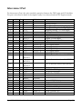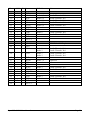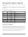
1
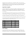
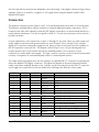
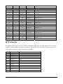
Danville Signal Processing, Inc.
dspstak™ c96k44
User Manual
Version 1.00
Danville Signal Processing, Inc.
dspstak™ c96k44 User Manual
Copyright © 2004 Danville Signal Processing, Inc. All rights reserved. Printed in the USA.
Under the copyright laws, this manual may not be reproduced in any form without prior written
permission from Danville Signal Processing, Inc.
Danville Signal Processing, Inc. strives to deliver the best product to our customers. As part of this
goal, we are constantly trying to improve our products. Danville Signal Processing, Inc., therefore,
reserves the right to make changes to product specification or documentation without prior notice.
Updated operating manuals and product specification sheets are available at our website for
downloading.
This manual may contain errors, omissions or “typo’s”. Please send your comments, suggestions and
corrections to:
Danville Signal Processing, Inc.
38570 100th Avenue
Cannon Falls, MN 55009-5534
Trademark Notice
dspstak is a trademark of Danville Signal Processing, Inc. VisualDSP++, and SHARC are trademarks
of Analog Devices, Inc. CyberClocks is a trademark of Cypress Semiconductor Corporation.
Contact Information
Danville Signal Processing, Inc.
38570 100th Avenue
Cannon Falls, MN 55009
E-mail:
Web Site:
[email protected]
http://www.danvillesignal.com
Voice:
Fax:
507-263-5854
877-230-5629
dspstak™ c96k44 User Manual
Page 2
Table of Contents
Overview ....................................................................................4
Introducing dspstak™.............................................................................4
dspstak™ c96k44...................................................................................4
Introduction...........................................................................................5
Hardware Description................................................................6
Wolfson WM8731 .................................................................................6
Input Buffer Amplifier ............................................................................7
Power Supply ........................................................................................7
Connectors ............................................................................................8
SPI Connector........................................................................................9
Interconnect Port .................................................................................10
Operating Modes & Register Configuration ............................12
Serial Interface Configuration ...............................................................12
Programmable Clocks ..........................................................................13
Operating Mode 0 ...............................................................................13
Operating Mode 1 ...............................................................................13
Operating Mode 2 ...............................................................................13
Codec Control Registers .......................................................................14
Software....................................................................................15
Schematic .................................................................................15
Mechanical Drawings...............................................................15
Accessories ...............................................................................15
Power Amplifier Module ......................................................................15
Extender Boards...................................................................................16
Product Warranty .....................................................................17
dspstak™ c96k44 User Manual
Page 3
Overview
DSP-based embedded applications often take the form of a digital signal processing engine coupled
with a specialized data conversion and signal conditioning front end. The front end electronics and
the DSP are almost always connected via high speed serial ports and the general purpose I/O ports
of the DSP. In most cases, once the local memory and peripheral interfacing needs of the DSP are
fulfilled, the DSP’s data and address busses are no longer needed.
Standardized bus architectures such as PC/104, PCI and cPCI are all based on communicating via
each board’s data and address bus, while ignoring the needs of the most DSP / data conversion
interfaces.
Introducing dspstak™
Danville’s dspstak modules are designed to simplify DSP-based embedded applications. Generally,
each dspstak consists of two modules: a DSP Engine, and a signal conditioning/data conversion I/O
Module. The Interconnect Port consists of SPORTs (high speed serial ports), SPI, general I/O, clocks
and power connections.
DSP Engine modules generally consist of a DSP processor, memory, power supplies and standard
digital I/O such as RS-232 and USB. We currently have products based on Analog Devices’ SHARC®
processors.
The I/O Modules may include signal conditioning electronics, A/D and/or D/A data converters,
audio transceivers, unique connectors and a plethora of other special front end requirements. Since
the I/O Module is separate from the DSP Engine Module, custom interfaces can be created quickly
and inexpensively. Danville has a number of standard I/O Modules and often is willing to create a
new one based on customer request. You can also create your own.
dspstak™ c96k44
This manual covers the dspstak c96k44 I/O Module and is complemented by the dspstak Family
Users Manual. The family manual covers topics that all dspstaks have in common. You will want to
review the family manual for mechanical dimensions, system configurations, basic connector
specifications, etc.
You will also need the relevant manuals and datasheets for the dspstak DSP Engine, the DSP
processor and the data converter. Links to these manuals and other resources are found on our
web site at http://www.danvillesignal.com/index.php?id=dspdev_links
dspstak™ c96k44 User Manual
Page 4
Intended Audience
The dspstak c96k44 is intended for DSP systems integrators, designers and programmers who may
wish to integrate a dspstak into their products. This manual is primarily aimed at users who have a
working knowledge of microcomputer technology and DSP related design. We assume that you are
familiar with the Analog Devices DSP used on the companion dspstak DSP Engine.
Introduction
The dspstak™ c96k44 is a 4 channel audio ADC & DAC I/O module based on a pair of sigma delta
stereo audio codecs. Assuming a 12.288MHz master clock, the c96k44 allows sampling rates from
8k to 96k. Other sampling rates are available by reprogramming the dspstak DSP Engine to another
master clock frequency. A special version of the c96k44 (opt 1) is available that allows two dspstak
c96k44 modules to be combined for 8 channel configurations all with synchronous sampling.
There are a number of additional accessory boards available for the dspstak c96k44 as well. These
include a small power amplifier module, BNC extender boards and 6.3mm phone jack extender
boards.
The dspstak c96k44 includes the following items:
Hardware:
•
dspstak™c96k44 board
Documents & Programs (CD):
•
•
•
This manual
dspstak Family User Manual
Device driver software
We recommend that you have the following tools and documents:
•
•
•
•
Analog Devices VisualDSP++™ for SHARC®
Wolfson WM8731 Data Sheet
Documentation for the companion dspstak DSP Engine
Cypress Semiconductor CyberClocks™
Our website (www.danvillesignal.com) has downloads and links to other supplementary tools and
documents.
dspstak™ c96k44 User Manual
Page 5
Hardware Description
The dspstak c96k44 I/O Module uses two Wolfson WM8731 codecs at its core. These codecs are
24 bit converters that can be used independently from each other to create two separate stereo
channels (perhaps programmed to different sample rates) or they can be combined to sample
coherently from the same clock. A variety of different sample rates are configurable under software
control. Master clocks (MCLK1 & MCLK0) can be programmed to allow just about any sampling
rate from 4k to 102.4k. A variety of sampling rate configurations are outlined later in this manual.
Each audio input is buffered by a low noise op amp stage. This op amp stage may be configured for
low noise electret microphone circuits including mic bias.
The following sections expand on the basic hardware of the dspstak c96k44:
•
•
•
•
•
Wolfson WM8731
Input Buffer Amplifier
Power Supply
Connectors
SPI Expansion
Wolfson WM8731
The WM8731 has a variety of connections and configurations, most which are completely ignored
by the c96k44. You may wish to look at the WM8731 datasheet block diagram while we discuss the
WM8731 signal flow and configuration used by the dspstak c96k44.
Each audio input is routed to one of the two line inputs of the WM8731. This allows each channel
to benefit from the built in PGA (programmable gain amplifier) available to the line inputs. Since the
MICIN does not have a PGA, it is not used by the dspstak c96k44. Microphone support is
accomplished by the Input Buffer Amplifier discussed in the next section.
Each input signal is converted by the internal ADC into 24 bit words that are transmitted in I2S
format. Details on the data interface are in the next section of this manual.
Audio data is sent by the DSP to the DAC section of the codec. The HP outputs are used since
these outputs have stepped attenuators available for level control. Since the line outputs do not
have programmable attenuators, they are ignored.
The control port of the WM8731 is used to configure the sampling rates, PGAs, attenuators and
other registers under software control. In the dspstak c96k44, these registers are all controlled by
the dspstak SPI port using the #SPI_SS chip select. Since as many as four WM8731 codecs can be
dspstak™ c96k44 User Manual
Page 6
programmed from the same #SPI_SS line, a special WM8731 address is used to activate each
individual slave select line before the SPI port can write a codec. Codecs can be written individually
or globally depending on the slave select mask. The software drivers included with the dspstak
c96k44 illustrate the process. Details on the dspstak c96k44 operating modes and this special
register are discussed later in this manual.
Input Buffer Amplifier
A fixed gain amplifier buffers each audio input. This amplifier is configured with a gain of either 1
(0dB) or 11 (+20.8dB). The unity gain setting is generally used for line level signals since the
internal PGA can be used to adjust the gain in 1.5dB steps. The +20.8dB setting is used for low
level signals such as electret microphones. Signal levels should be restricted to +/- 1.4V full scale
(1V rms sinusoid) .
If you are using typical electret microphones (two wire circuits), you can add a DC bias for each
input by adding a shorting jumper to its corresponding Bias jumper location on JH3. Likewise, you
can increase the gain of a channel by adding a shorting jumper to its Gain jumper location on JH3.
For example a shorting jumper on Gain3 and Bias3 will cause Input 3 to have an input gain of
20.8dB with microphone biasing. The other inputs would be configured as 0dB with no mic biasing.
The microphone bias supply (3V DC) without the typical 3K limiting resistor is also available on the
connector pins adjacent to each audio input pin. This allows three wire microphone circuits to be
supported as well as the more common two wire circuits.
Pin
1&2
3&4
5&6
7&8
9&10
11&12
13&14
15&16
Name
Open
Short
Gain – Audio In 3
Mic Bias – Audio In 3
Gain – Audio In 2
Mic Bias – Audio In 2
Gain – Audio In 1
Mic Bias – Audio In 1
Gain – Audio In 0
Mic Bias – Audio In 0
0dB
No
0dB
No
0dB
No
0dB
No
+20.8dB
Yes
+20.8dB
Yes
+20.8dB
Yes
+20.8dB
Yes
Power Supply
The dspstak c96k44 derives its operating power from its companion dspstak DSP Engine. The
dspstak c96k44 operates entirely on a single positive supply. We recommend a 9VDC supply for
the dspstak when operating in a c96k44 + DSP Engine configuration. Higher supply voltages may
dspstak™ c96k44 User Manual
Page 7
also be used with increased power dissipation since the analog 5 volt supply is derived using a linear
regulator. There is no need for a negative or AC supply when using the dspstak c96k44 with a
dspstak DSP Engine.
Connectors
The primary connector on the c96k44 is JH1, a 34 pin latching dual row header (0.100 inch pitch).
This allows a standard ribbon cable to interface to external input and output connections. JH1 is
located on the side of the dspstak so that the DSP Engine connections can be mounted directly to a
panel without interference. It is also low profile so that 1U 19 inch rack enclosures can be used as a
possible enclosure.
In most applications, only connections on pins 15 through 34 are used. These are audio input and
audio output connections with ground returns for each channel. Pins 1 through 14 are used for
digital I/O connections and power supply fan out. Many of these connections are also available on
the SPI expansion connector JH2. The dspstak c96k44 (Opt 1) uses a 20 pin latching dual row
header instead of the 34 pin header used in the standard product. This connector is used
exclusively for audio inputs and outputs. The Opt 1 version is used to create 8 channel systems and
is always a companion to a standard dspstak c96k44 (3 board dspstak system).
The audio inputs and outputs may also be routed to an optional DB-37F connector located directly
above the dspstak DSP Engine connectors. This allows the dspstak to be panel mounted with the
audio connections available directly to the “outside” world. Unused pins on the DB-37F connector
are brought out to pads that can be user defined by soldering wires directly to these pads.
JH1
1
2
3
4
5
6
7
8
9
10
11
12
13
14
15
JH1 Opt 1
1
dspstak™ c96k44 User Manual
J1
Name
11
29
DGND
SPI SI
#SPI SS1
#SPI SS2
SPI CLK
SPI SO
LED4
LED3
LED2
LED1
LED0
Va+
VaAGND
Audio Out 0
Notes
IO5
IO6
100 Ohm Series Resistor
237 Ohm Series Resistor
237 Ohm Series Resistor
237 Ohm Series Resistor
237 Ohm Series Resistor
Unregulated Positive Supply
Unregulated Negative Supply
Left Ch U2
Page 8
JH1
JH1 Opt 1
J1
Name
16
17
18
19
20
21
22
23
24
25
26
27
28
29
30
31
32
33
34
2
3
4
5
6
7
8
9
10
11
12
13
14
15
16
17
18
19
20
10
28
9
27
8
26
7
25
6
24
5
23
4
22
3
21
2
20
1
AGND
Audio Out 1
AGND
Audio Out 2
AGND
Audio Out 3
AGND
AGND
Audio In 0
Mic Bias 0
Mic Bias 1
Audio In 1
AGND
AGND
Audio In 2
Mic Bias 2
Mic Bias 3
Audio In 3
AGND
Notes
Right Ch U2
Left Ch U3
Right Ch U3
Left Ch U2
Right Ch U2
Left Ch U3
Right Ch U3
SPI Connector
The dspstak c96k44 has a 10 pin 0.100 box header for digital I/O and SPI expansion. Do not drive
long lines without buffers from this connector or the SPI interface may fail to operate correctly for
local resources due to excessive capacitance loading.
Pin
Name
1
2
3
4
5
6
7
8
9
10
#RESET
DGND
#SPISS3
SPISO
#SPISS2
SPICLK
SPISI
#SPISS1
Vd+5
Vd+3.3
Notes
IO7
MISO
IO6
MOSI
IO5
dspstak™ c96k44 User Manual
Page 9
Interconnect Port
The Interconnect Port is the only standard connection between the DSP Engine and I/O Modules.
This port is described in detail in the dspstak Family Users Manual and the DSP Engine manuals.
Row
A&C
B
Name
1
2
3
4
5
*
*
*
*
*
*
*
*
*
*
AGND
Va+
VaVa+5
AGND
6
7
8
*
*
*
*
*
*
Vd+5
Vd+3.3
DGND
JH2 Only
Digital 5.0 Volt Supply
Digital 3.3 Volt Supply
Digital Ground – Main Return
9
9
10
10
11
11
*
LED0
LED1
LED2
LED3
LED4
IO5
(#SPISS1)
IO6
(#SPISS2)
IO7
(#SPISS3)
#SPI_SS
SPICLK
SPISO
SPISI
IRQ
#RESET
SYSCLKIN
SYSCLKOUT
JH1 (237 R)
JH1 (237 R)
JH1 (237 R)
JH1 (237 R)
JH1 (100 R)
3.3V Digital Output
3.3V Digital Output
3.3V Digital Output
3.3V Digital Output
3.3V Digital Output
(IO5 is alternate function with #SPISS1)
12
*
*
*
*
*
*
12
13
13
14
14
15
15
16
16
17
17
18
18
*
*
*
*
*
*
*
*
*
*
*
*
*
Vd+3.3
GND
DRA0
DTA0
dspstak™ c96k44 User Manual
C96k44
Notes
JH1 Only
Analog Ground
Unregulated Positive Analog Supply
Unregulated Negative Analog Supply
Regulated Analog +5.0 Volt Supply
Analog Ground
(IO6 is alternate function with #SPISS2)
(IO7 is alternate function with #SPISS3)
WM8731 SS
JH2 Only
NC
JH2 Only
Primary SPI Slave Select
SPI Clock – DSP Engine is Master
SPI Serial Out (MISO)
SPI Serial In (MOSI)
External DSP Clock Input
Programmable clock
SPORT 0 – Full Duplex
Mode 0,2
Mode 0,2
Audio Channels 1&2
Audio Channels 1&2
Page 10
Row
A&C
19
19
20
20
21
21
22
22
23
23
24
24
*
25
25
26
*
*
*
*
*
*
*
*
*
*
*
*
*
*
26
27
27
28
28
29
29
30
30
31
31
32
32
B
*
*
*
*
*
*
*
*
*
*
*
*
*
Name
GND
MCLK0
RFS0
TFS0
RCLK0
TCLK0
#RESET0
GND
DTB0
DRB0
GND
Vd+3.3
Vd+3.3
GND
DRA1
DTA1
GND
MCLK1
RFS1
TFS1
RCLK1
TCLK1
#RESET1
GND
DTB1
DRB1
GND
Vd+3.3
dspstak™ c96k44 User Manual
C96k44
Notes
Mode 0,2
Mode 0,2
Mode 0,2
Mode 0,2
Mode 0,2
NC
Audio Channels 1&2
Audio Channels 1&2
Audio Channels 1&2
Audio Channels 1&2
Audio Channels 1&2
Mode 0
Mode 0
Audio Channels 3&4
Audio Channels 3&4
SPORT 1 – Full Duplex
Mode 1
Mode 2
Mode 1
Mode 2
Audio Channels 1&2
Audio Channels 3&4
Audio Channels 1&2
Audio Channels 3&4
Mode 1,2
Optional
Mode 2
Mode 2
NC
Audio Channels 1&2
Audio Channels 1&2
Mode 2
Mode 2
Audio Channels 3&4
Audio Channels 3&4
Page 11
Operating Modes & Register Configuration
The dspstak c96k44 has three different operating modes. The configuration jumpers on JH5 select
the operating mode.
The primary codec, U2 is mapped to audio channels 0 and 1. The secondary codec, U3 is mapped
to audio channels 2 and 3. Each codec is mapped to different SPORT connections depending on
the operating mode.
U2 always uses MCLK0 as its master clock. U3 may use either MCLK0 or MCLK1 as its master clock.
This choice is made via a shorting jumper on JH5.
Name
Mode 0
Mode 1
Mode 2
Mode 3
Name
ILLEGAL!
MCLK1 Select
MCLK0 Select
ILLEGAL!
CFG1
Pins 3&4
CFG0
Pins 1&2
Short
Short
Open
Open
Short
Open
Short
Open
MCLK1
Pins 5&6
MCLK0
Pins 9&10
Short
Short
Open
Open
Short
Open
Short
Open
Notes:
U2 Master, U3 Slave
U2, U3 Slave (used by c96k44 – Opt 1)
U2 Master, U3 Master
Reserved
Notes:
Will Short Clocks!
U3 uses MCLK1 – Use only with Mode 2
U3 uses MCLK0
Codecs won’t operate!
Pins 7&8 of JH5 are ignored. They are connected to GND.
Serial Interface Configuration
The dspstak c96k44 uses I2S interfacing for its audio data interface. In all cases, at least one codec
acts as an I2S master. The DSP is always configured as an I2S slave. Although the WM8731 supports
a variety of different audio data interfaces, for the purposes of the dspstak c96k44, the interface
transmits and receives 32 bit words for each channel. Unused bits are generally padded with zeros.
The WM8731 registers must be configured correctly depending on the desired Operating Mode.
The software drivers supplied with the c96k44 will help you with these settings.
dspstak™ c96k44 User Manual
Page 12
Programmable Clocks
Although a codec is always the I2S master, the master clock (MCLK0 or MCLK1) is always provided
by the programmable clock on the dspstak DSP Engine. These clocks are very flexible and may be
set to just about any desired clock for your application. Consult the dspstak DSP Engine manual to
reconfigure these clocks for your application.
Operating Mode 0
Operating Mode 0 uses only one full duplex SPORT. This SPORT is called SPORT0 on the dspstak
Interconnect Port but is likely to be derived from two half duplex SPORTs in the DSP. Audio
channels 0&1 (U2) are mapped to the DRA0 and DTA0 lines and audio channels 2&3 (U3) are
mapped to the DRB0 and DTB0 lines.
All channels sample at the same time and must be set to the same sampling rate. The primary codec
U2 acts as the I2S master. All timing is derived from U2, therefore U3 must be configured as an I2S
slave. MCLK0 should be selected for U3.
Operating Mode 1
Operating Mode 1 is a companion mode to Mode 0. Like Mode 0, it also uses only one full duplex
SPORT, but in this case: SPORT1. Mode 1 is normally used with a dspstak c96k44 Opt 1. The
Option 1 board differs from the standard dspstak c96k44 in that it has a special male/female
stacking DIN connector for the Interconnect Port. This allows the c96k44 to be used in a three
board dspstak configuration, two dspstak c96k44s (Std & Opt 1), and a dspstak DSP Engine. This
creates an eight channel system.
Mode 1 always assumes that there is another dspstak c96k44 board operating in Mode 0. The
“Mode 0” dspstak c96k44 acts as the I2S master (via its primary codec, U2). Both codecs on the
“Mode 1” dspstak are I2S slaves.
Audio channels 0&1 (U2) are mapped to the DRA1 and DTA1 lines and audio channels 2&3 (U3)
are mapped to the DRB1 and DTB1 lines.
All channels sample at the same time and must be set to the same sampling rate. This includes the
other dspstak c96k44 operating in Mode 0. MCLK0 should be selected for U3.
Operating Mode 2
Operating Mode 0 uses two full duplex SPORTs. These SPORTs are called SPORT0 and SPORT1
on the dspstak Interconnect Port but are likely to be derived from four half duplex SPORTs in the
dspstak™ c96k44 User Manual
Page 13
DSP. Audio channels 0&1 (U2) are mapped to the DRA0 and DTA0 lines and audio channels 2&3
(U3) are mapped to the DRA1 and DTA1 lines.
In Mode 2, each codec is configured independently as an I2S master. This allows each codec to
operate completely independently. You can have different sample rates for each codec. You can
also program MCLK1 to be used as the master clock for U3. This means that you can have very
different sample rates for each codec. For example, if MCLK1 is set to 19.6608MHz and MCLK0 is
set to 18.432 MHz, you could be sampling channels 0&1 at 96k and channels 2&3 at 102.4k.
Codec Control Registers
Each WM8731 codec is configured via SPI. It is a write-only interface that is used to set the
sampling rate, configure the codec for the correct data interface, and adjust gain, attenuation and
other operating parameters. These registers are described in the WM8731 datasheet and
implemented in the dspstak c96k44 device drivers and example code.
The dspstak c96k44 maps all the control ports to a single SPI SS line. This creates a problem since
there can be as many as four codecs in a c96k44 configuration and you don’t necessarily want to
write all the devices with the same data.
This situation was solved on the dspstak c96k44 by creating a new command on the WM8731.
WM8731 commands are always at addresses less that 0x8000. In other words, Bit 15 is always 0.
We take advantage of this situation by creating a new command at address 0x8000 (This would
correspond to register (80h) in Wolfson documentation). The WM8731 ignores a command with
this address.
Command 0x8000 is used to set the individual SPI SS lines on each codec. Bits 0 through 3 are
used for this purpose where 1 is true.
Bit 0 – Select the primary codec (U2) mapped to Sport 0
Bit 1 – Select the secondary codec (U3) mapped to Sport 0
Bit 2 – Select the primary codec (U2) mapped to Sport 1
Bit 3 – Select the secondary codec (U3) mapped to Sport 1
This translates as follows:
Bit 0 & Bit 1 select U2 & U3 respectively in Mode 0
Bit 2 & Bit 3 select U2 & U3 respectively in Mode 1
Bit 0 & Bit 3 select U2 & U3 respectively in Mode 2
The SPI_SS line must be active (low) to select any codec regardless of the state of the 0x8000
register.
dspstak™ c96k44 User Manual
Page 14
Software
The Distribution CD includes software examples and device drivers that simplify the configuration
of the dspstak c96k44. You may use these examples as take off points to start your own
applications.
Our software library is constantly expanding. This code and other resources are available to our
customers through our web site. Send an email to [email protected] to gain access to the
customer section of our web site.
Schematic
The Distribution CD includes a schematic diagram of the dspstak c96k44 in file sch_c96k44.pdf
Mechanical Drawings
Mechanical Drawings are included in the dspstak Family Users Manual. If you any need additional
information on board mounting, clearances, etc, send an email to [email protected].
The dspstak can be incorporated into products in a variety of different ways. If you want to use the
dspstak in an unusual configuration, you may want to check with us for suggestions, design review,
etc.
Accessories
The following accessories are available for the dspstak c96k44:
•
•
•
dspstak c96k44 – BNC Extender
dspstak c96k44 – 6.3mm Phone Jack Extender
dspstak c96k44 – Power Amplifier
Power Amplifier Module
A stereo power amplifier module is available that plugs into unused connectors on the dspstak
c96k44. Since the power amplifier can draw significant current, the dspstak Engine may need to be
modified with higher current rectifiers as well. Check with Danville if you are interested .
dspstak™ c96k44 User Manual
Page 15
Extender Boards
Each extender board is designed to expand the latching header into 8 separate connectors. In the
BNC case, the three wire microphone bias circuit is not available. The 6.3mm (1/4’) phone jack
version can supply the microphone bias on the ring if desired. The extender boards do not connect
to the optional digital I/O, only the audio inputs and outputs are used.
In the standard version, a 20 pin right angle female dual row header connects directly to the
latching header. The extender boards can also be supplied with a 20 pin latching header. This
would also require a ribbon cable (34 pin to 20 pin for standard c96k44 boards) to connect the
boards.
The extender boards can also be assembled to use a mating DB-37M connector. All variations of
the extender board are the same price.
dspstak™ c96k44 User Manual
Page 16
Product Warranty
Danville Signal Processing, Inc. products carry the following warranty:
Danville Signal Processing products are warranted against defects in materials and workmanship. If
Danville Signal Processing receives notice of such defects during the warranty period, Danville
Signal Processing shall, at its option, either repair or replace hardware products, which prove to be
defective.
Danville Signal Processing software and firmware products, which are designated by Danville Signal
Processing for use with our hardware products, are warranted not to fail to execute their
programming instructions due to defects in materials and workmanship. If Danville Signal Processing
receives notice of such defects during the warranty period, Danville Signal Processing shall, at its
option, either repair or replace software media or firmware, which do not execute their
programming instructions due to such defects. Danville Signal Processing does not warrant that
operation of the software, firmware, or hardware shall be uninterrupted or error free.
The warranty period for each product is one year from date of installation.
Limitation of Warranty:
The forgoing warranty shall not apply to defects resulting from:
•
•
•
•
•
Improper or inadequate maintenance by the Buyer;
Buyer-supplied software or interfacing;
Unauthorized modification or misuse;
Operation outside the environmental specification of the product;
Improper site preparation and maintenance.
Exclusive Remedies:
The remedies provided herein are the Buyer’s sole and exclusive remedies. In no event shall
Danville Signal Processing, Inc. be liable for direct, indirect, special, incidental or consequential
damages (including loss of profits) whether based on contract, tort, or any other legal theory.
dspstak™ c96k44 User Manual
Page 17