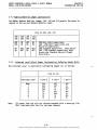
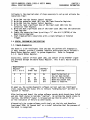
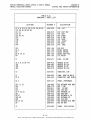
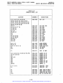
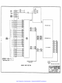
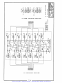
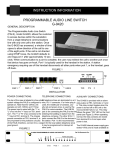
1
Artisan Technology Group is your source for quality
new and certified-used/pre-owned equipment
• FAST SHIPPING AND
DELIVERY
• TENS OF THOUSANDS OF
IN-STOCK ITEMS
• EQUIPMENT DEMOS
• HUNDREDS OF
MANUFACTURERS
SUPPORTED
• LEASING/MONTHLY
RENTALS
• ITAR CERTIFIED
SECURE ASSET SOLUTIONS
SERVICE CENTER REPAIRS
Experienced engineers and technicians on staff
at our full-service, in-house repair center
WE BUY USED EQUIPMENT
Sell your excess, underutilized, and idle used equipment
We also offer credit for buy-backs and trade-ins
www.artisantg.com/WeBuyEquipment
InstraView REMOTE INSPECTION
LOOKING FOR MORE INFORMATION?
Visit us on the web at www.artisantg.com for more
information on price quotations, drivers, technical
specifications, manuals, and documentation
SM
Remotely inspect equipment before purchasing with
our interactive website at www.instraview.com
Contact us: (888) 88-SOURCE | [email protected] | www.artisantg.com
Acromag
m"
Series 935x4
VME Isolated Analog 110 Card
Series 9450-1
VME General Purpose Isolated Digital 110 Card
Series 9510-X
VME Multi-Function Card
USER'S MANUAL
ACROMAG INCORPORATED
30765 South Wixom Road
P.O. BOX 437
Wixom, MI 48393-7037 U.S.A.
Tel: (248) 624-1541
Fax: (248) 624-9234
Artisan Technology Group - Quality Instrumentation ... Guaranteed | (888) 88-SOURCE | www.artisantg.com
SERIES AVME935X-I/9450-I/9510-X USER'S MANUAL
VMEbus ISOLATION BOARDS
TABLE OF CONTENTS
The information in this document is subject to change without notice.
Acromag, Inc. makes no warranty of any kind with regard to this material,
including but not limited to, the implied warranties of merchantability and
fitness for a particular purpose. Acromag, Inc. assumes no responsibility for
any errors that may appear in this document and makes no commitment to update
nor to keep current the information contained in this document.
I
-
IMPORTANT SAFETY CONSIDERATIONS
I
It is very important for the user to consider the possible adverse effects of
power, wiring, component, sensor, or software failures in designing any type
of control or monitoring system. This is especially important where economic
property loss or human life is involved. It is important that the user
employ redundancy, and comprehensive failure analysis to insure a safe and
satisfactory overall system design. It is agreed between the Buyer and
Acromag, that this is the Buyer's responsi bi 1 i ty.
.
Acromag , Inc
30765 South Wixom Road
P.O. Box 437
Wixom, Michigan 48393-7037, USA
Tel: (248) 624-1541
Fax: (248) 624-9234
Copyright 1991, 1993, 1994 Acromag, Inc. Printed in USA.
Data and specifications subject to change without notice.
Artisan Technology Group - Quality Instrumentation ... Guaranteed | (888) 88-SOURCE | www.artisantg.com
SERIES AVME935X-I/945O- I/9510-X USER'S MANUAL
VMEbus ISOLATION BOARDS
TABLE OF CONTENTS
CHAPTER
1.0 GENERAL INFORMATION
1.1
1.2
1.3
1.4
1.5
1.6
Introduction . . . . . . . . . . . . . . .
Analog Input Features ( 935X-I & 9510-X ) .
Analog Output Features ( 9351-1 & 9510-X ) .
Digital 1/0 Features ( 9450-1 & 9510-X ) .
VMEbus Interface Features . . . . . . . . .
Field Compatibility . . . . . . . . . . . .
1.6.1 Analog Inputs and Outputs
1.6.2 Digital Inputs and Outputs
.........
.........
.........
.........
.........
.........
..............
..............
1-1
1-1
1-2
1-2
1-2
1-3
1-3
1-3
2.0 PREPARATION FOR USE
..................
..................
..................
Default Jumper Configuration . . . . . . . . . . . . .
2-1
2-1
2-1
.....
2-2
2-2
2-3
2.1 Unpacking and Inspection
2.2 Card Cage Considerations
2.3 Board Configuration . .
2.3.1
2.3.1.1 Analog Input Default Configuration
2.3.1.2 Analog Output Default Configuration
2.3.1.3 Digital 1/0 Default Configuration .
2.4
2.5
.....
.....
VMEbus Configuration . . . . . . . . . . . . . . . . . . . .
2.4.1 Address Decode Jumper Configuration . . . . . . . . .
2.4.2 Address Modifier Jumper Configuration . . . . . . . .
2.4.3 Interrupt Level Select Jumper Configuration . . . . .
Analog Input Configuration ( 935X-I & 9510-X ) . . . . . . . .
2.5.1 Analog Input Type Jumper Configuration . . . . . . . .
2.5.2 Analog Input Ranges Jumper Configuration . . . . . . .
2.5.3 Analog Input Data Format Jumper
Configuration . . . . . . . . . . . . . . . . . . . .
2.5.3.1
2.5.3.2
Unipolar Straight Binary (USB)
Analog Input Data Format . . .
Bipolar Offset Binary (BOB) and
Bi pol ar Two ' s Compl ement (BTC)
Analog Input Data Format . . .
2.5.4 Analog Input "Live" End Points of Span
Configuration . . . . . . . . . . . .
2-1
2-5
2-5
2-6
2-6
2-7
2-7
2-7
2-9
.......
2-9
.......
2-9
........
Artisan Technology Group - Quality Instrumentation ... Guaranteed | (888) 88-SOURCE | www.artisantg.com
2-10
SERIES AVME935X-I/9450-I/9510-X USER'S MANUAL
VMEbus ISOLATION BOARDS
TABLE OF CONTENTS
CHAPTER
2.5.4.1
2.5.4.2
2.5.5
2.6
Analog I n p u t R e s i s t o r Programmable Gain
Analog Output C o n f i g u r a t i o n ( 9351-1 & 9510-X )
2.6.1
2.6.2
2.7
.
.
.
.......
2.7.5.2
Digital
2.7.6.1
2.7.6.2
2.7.7
.
.
.
.
.
.
.
.
.
.
..
..
..
..
..
.
.
.
.
.
.
.
.
....
....
....
....
.......
Configuring f o r
S o l i d s t a t e Relays
C o n f i g u r i n g t h e PB16A Termination
Panel . . . . . . . . . . . . . .
.............
......
1/0 Use With Other Devices . . . . . . . . . .
Re1ay C o i l s and Other I n d u c t i v e Loads . . . .
Contact Closures and Switches . . . . . . . .
D i g i t a l 1/0 P u l l - u p Voltage Jumper
Configuration
Connectors
2.8.1
2.8.2
2.8.3
2.8.4
.
...
...
...
. . . . . . . .
D i g i t a l 1/0 I n p u t F i l t e r i n g . . . . . .
D i g i t a l 1/0 Adjustable H y s t e r e s i s P o i n t
D i g i t a l 1/0 W r i t e and Read Back Timing .
D i s a b l i n g t h e Output D r i v e r s
D i g i t a l 1/0 Use With S o l i d S t a t e Relays
2.7.5.1
2.7.6
.....
Analog Output Range Jumper C o n f i g u r a t i o n
Analog Output Data Format Jumper C o n f i g u r a t i o n
D i g i t a l 1/0 C o n f i g u r a t i o n ( 9450-1 & 9510-X )
2.7.1
2.7.2
2.7.3
2.7.4
2.7.5
2.8
" L i v e " End P o i n t Range Analog I n p u t
f o r U n i p o l a r S t r a i g h t B i n a r y Data .
" L i v e " End P o i n t Range f o r Analog
I n p u t B i p o l a r O f f s e t B i n a r y and
B i p o l a r Two's Complement Data . . .
....................
.........................
.
.
...
.......
Analog Input/Output Connector
D i g i t a l Input/Output Connector
External T r i g g e r Connector
VMEbus Connections
.
.
.
.
.
.
.
.
.
.
.
.
.
.
.
.
.
.
.
.
......
......
......
......
.................
....................
...............
2.9 Power-Up Timing and Loading
2.10 Data T r a n s f e r Timing
2.11 F i e l d Grounding Considerations
3.0
PROGRAMMING INFORMATION
3.1
Memory Map
.........................
Artisan Technology Group - Quality Instrumentation ... Guaranteed | (888) 88-SOURCE | www.artisantg.com
SERIES AVME935X-I/9450-I/9510-X USER'S MANUAL
VMEbus ISOLATION BOARDS
TABLE OF CONTENTS
CHAPTER
PAGE
..............
...............
Status Bits Usage . . . . . . . . . . . . . .
3.1.1 Board Identification PROM
3.1.2 Board Status Register . .
3.1.2.1
3.1.3 Vector Register . . . . . .
3.1.4 Board Control Register . .
3.1.5 Channel Register . . . . .
3.1.6 Counter Control Register .
3.1.7 Scan Counter Register . . .
3.1.8 Timer Prescaler Register .
3.1.9 Conversion Timer Register .
3.1.10 Conversion Status Register
3.1.11 Start Conversion Register .
3.1.12Analog Input Data Register
3.1.13 Analog Output Data Register
3.1.14 Digital 1/0 Port Registers
3.2
3.3
..............
..............
..............
..............
..............
..............
..............
..............
..............
..............
..............
..............
Modes of Operation For A/D Conversion ( 935X-I & 9510-X ) . . .
3.2.1 Channel Mode . . . . . . . . . . . . . . . . . . . . .
3.2.2 ScanMode . . . . . . . . . . . . . . . . . . . . . . .
Initiating Analog-to-Digital Conversions ( 935X-I & 9510-X ) .
.........
.........
.........
General Programming Considerations . . . . . . . . . . . . . .
3.4.1 Board Diagnostics . . . . . . . . . . . . . . . . . . .
3.4.2 The Analog to Digital Conversion Sequence . . . . . . .
3.4.3 Treatment of Data . . . . . . . . . . . . . . . . . . .
3.4.4 Analog Input Throughput Rate . . . . . . . . . . . . .
3.3.1 Software Triggering . Register Access
3.3.2 External Triggering . TTL Input . . .
3.3.3 Timed Periodic Triggering . . . . . .
3.4
4.0 PRINCIPLES OF OPERATION
4.1
4.2
4.3
4.4
Introduction . . . . . . . . . . . . . . . .
VMEbus Interface . . . . . . . . . . . . . .
Register Location . . . . . . . . . . . . . .
Isolation Barrier ( 935X.1, 9450-1 & 9510-1 )
4.4.1
4.4.2
4.4.3
........
........
........
........
Optical Isolation . . . . . . . . . . . . . . . . . .
Isolated Data Transfer Controller . . . . . . . . . .
Power Isolation . . . . . . . . . . . . . . . . . . .
Artisan Technology Group - Quality Instrumentation ... Guaranteed | (888) 88-SOURCE | www.artisantg.com
SERIES AVME935X-I/9450-I/9510-X USER'S MANUAL
VMEbus ISOLATION BOARDS
TABLE OF CONTENTS
.
PAGE
CHAPTER
4.5 Analog Input Section ( 935X-I & 9510-X ) .
4.6
4.7
5.0
..........
Analog Input Multiplexer . . . . . . . . . . . . . . .
Instrumentation Amplifier . . . . . . . . . . . . . .
Programmable Gain Circuit . . . . . . . . . . . . . .
Sample and Hold Amplifier . . . . . . . . . . . . . .
Analog-to-Digital Converter . . . . . . . . . . . . .
Conversion Control Circuits . . . . . . . . . . . . .
External Trigger . . . . . . . . . . . . . . . . . . .
Timed Periodic Trigger Circuit . . . . . . . . . . . .
Scan Mode Counter Circuits . . . . . . . . . . . . . .
Analog Output Section ( 9351-1 & 9510-X ) . . . . . . . . . .
Digital Input/Output Section ( 9450-1 & 9510-X ) . . . . . . .
4-3
4-3
4-4
4-4
4-4
4-4
4-4
4-5
4-5
4-5
4-6
4-6
SERVICE AND REPAIR INFORMATION
5.1 Service and Repair Assistance . . . . . . . . .
5.2 Preliminary Service Procedure . . . . . . . . .
5.3 Calibration of Analog Input ( 935X-I & 9510-X )
5.3.1
5.3.2
5.3.3
5.3.4
5.3.5
5.4
.......
Analog Input Offset Calibration
for the Programmable Gain Stage . . . . .
Analog Input Standard Bipolar Calibration
Analog Input Standard Unipolar Calibration
Analog Input Live End Point Bipolar
Calibration . . . . . . . . . . . . . . .
Analog Input Live End Point Unipolar
Calibration . . . . . . . . . . . . . . .
Calibration of Analog Outputs ( 9351-1 & 9510-X )
5.4.1
5.4.2
5.5
.......
.......
Analog Output Bipolar Calibration
Analog Output Unipolar Cal i bration
PartsLists
......
......
......
......
......
......
..........
..........
.........................
5-1
5-1
5-1
5-2
5-2
5-3
5-3
5-4
5-4
5-5
5-6
5-6
6.0 SPECIFICATIONS
7.0
DRAWING AND SCHEMATIC
7.1 Part Location Drawing
7.2 Schematic . . . . . .
....................
....................
7-1
7-2
Artisan Technology Group - Quality Instrumentation ... Guaranteed | (888) 88-SOURCE | www.artisantg.com
-
SERIES AVME935X-I/9450-I/9510-X USER'S MANUAL
VMEbus ISOLATION BOARDS
TABLE OF CONTENTS
LIST OF FIGURES
2.1
2.2
2.3
2.4
2.5
2.6
2.7
3.1
3.2
3.3
3.4
4.1
7.1
PAGE
.
. . . . . . . . . . . . . . . . . . . . . . 2-4
. . . . . . . . . . . . . . . . . 2-8
. . . . . . . . . . . . . . 2-14
. . . . . . . . . . . . . . . . . . 2-18
. . . . . . . . . . . . . . . . . . . . 2-20
. . . . . . . . . . . . . . 2-20
. . . . . . . . . . . . . . . . . . . 2-27
Board Memory Map . . . . . . . . . . . . . . . . . . . . . . . . . 3-3
. . . . . . . . . . . . . . . . . . . . 3-5
Board I d e n t i f i c a t i o n Prom
Timing Diagram . . . . . . . . . . . . . . . . . . . . . . . . . . 3-16
Missed T r i g g e r Timing Diagram . . . . . . . . . . . . . . . . . . . 3-17
Block Diagram . . . . . . . . . . . . . . . . . . . . . . . . . . . 4-2
Schematic/Part Location . . . . . . . . . . . . . . . . . . . . . . 7 - 1
Jumper Location Drawing
Analog I n p u t F i e l d C o n f i g u r a t i o n s
S i m p l i f i e d D i g i t a l 1/0 P o i n t Schematic
S o l i d S t a t e Relay C o n f i g u r a t i o n
Relay D r i v e r C o n f i g u r a t i o n
Contact Closure C o n f i g u r a t i o n . . . . .
F i e l d Grounding Consideration
LIST OF TABLES
2.1
2.2
2.3
. . . . . . . . . . . . . . . . . . . . . . . . . . . 2-22
. . . . . . . . . . . . . . . . . . . . . . . . . 2-23
. . . . . . . . . . . . . . . . . . . . . . . . . . 2-25
P a r t s L i s t . . . . . . . . . . . . . . . . . . . . . . . 5-7
P a r t s L i s t . . . . . . . . . . . . . . . . . . . . . . . 5-10
P a r t s L i s t . . . . . . . . . . . . . . . . . . . . . . . 5-13
P a r t s L i s t . . . . . . . . . . . . . . . . . . . . . . . 5-15
P2Connector
P4 (P5) Connector
PlBusSignals
5.1AAVME9350.1
5.1BAVME9351.1
5.1CAVME9450.1
5.1DAVME9510.1
5.1E AVME9510 P a r t s L i s t
. . . . . . . . . . . . . . . . . . . . . . . . 5-18
Artisan Technology Group - Quality Instrumentation ... Guaranteed | (888) 88-SOURCE | www.artisantg.com
SERIES AVME935X-I/9450-I/9510-X USER'S MANUAL
VMEbus ISOLATION BOARDS
CHAPTER 1
GENERAL INFORMATION
1.1 INTRODUCTION
The AVME935X-I/9450-I/9510-X Series o f VME cards o f f e r a v a r i e t y o f f e a t u r e s
which make them an i d e a l choice f o r a broad spectrum o f Data A q u i s i t i o n and
Control Appl i c a t i o n s . The f o l l o w i n g t a b l e high1 i g h t s these f e a t u r e s .
ANALOG
INPUTS
ANALOG
OUTPUTS
DIGITAL
I/O
General Features
- A l l Analog Inputs, Analog Outputs and D i g i t a l I n p u t s and Outputs are
I s o l a t e d as a group from t h e VMEbus (except model AVME9510).
- BYTE o r WORD d a t a t r a n s f e r s .
- PASS/FAIL s t a t u s i n d i c a t o r LEDs on t h e f r o n t panel.
1.2
ANALOG INPUT FEATURES ( 935X-I & 9510-X )
- High l e v e l i n p u t s
- 16 d i f f e r e n t i a l / 3 2 single-ended (jumper s e l e c t a b l e ) .
- High speed successive approximation 12 b i t A/D c o n v e r t e r f o r a maximum
throughput time o f 32 microseconds p e r conversion.
- Jumper s e l e c t a b l e i n p u t ranges o f +10V, 0-10V and +5V.
- Software programmable gains o f 1, 2, 4, and
-
8.
R e s i s t o r programmable gains o f 1 t o 1000 ( s p e c i a l o r d e r ) .
- E x t e r n a l t r i g g e r i n p u t c a p a b i l i t y f o r s y n c h r o n i z a t i o n o f t h e conversion
sequence t o e x t e r n a l events.
- Hardware Timed P e r i o d i c Conversion capabi 1it y f o r p r e c i s e sampl i n g
i n t e r v a l s.
Artisan Technology Group - Quality Instrumentation ... Guaranteed | (888) 88-SOURCE | www.artisantg.com
CHAPTER 1
GENERAL INFORMATION
SERIES AVME935X- I/945O- I/9510-X USER'S MANUAL
VMEbus ISOLATION BOARDS
-
F i e l d connections accessible through the P2 connector.
User c a l i b r a t i o n f o r " l i v e end-points" o f spans.
- Scan Mode f o r e f f i c i e n t scanning o f sequential channels.
1.3
ANALOG OUTPUT FEATURES ( 9351-1 & 9510-X )
-High l e v e l voltage outputs - 2 channels.
-12 b i t D/A conversion w i t h s e t t l i n g time o f 6 microseconds.
- F i e l d connections accessible through the P2 connector.
-Jumper s e l e c t a b l e output ranges o f +10V, +5V, +2.5V,
1.4
0 t o t5V, 0 t o t10V.
DIGITAL 1/0 FEATURES ( 9450-1 & 9510-X )
-32 programmable 1/0 p o i n t s ( l i n e s ) configured as f o u r
-
8 b i t ports.
- A b i l i t y t o read back output states.
-Outputs s i n k up t o 100 mA, from up t o a 30 V source.
- B u i l t - i n p r o t e c t i o n diodes f o r d r i v i n g re1ay c o i l s .
-Input f i l t e r i n g (by i n s t a l 1 i n g c a p a c i t o r networks, see Section 2.7.1).
- I n p u t range o f 0 t o 30 v.
-Input h y s t e r e s i s (0.3 V o l t s )
.
- I n p u t t h r e s h o l d adjustable (by i n s t a l l i n g Resistor Networks, see Section
2.7.2).
-Cornpati b l e w i t h i n d u s t r y standard sol i d s t a t e re1ays and t e r m i n a t i o n panel s,
PBl6A.
- F i e l d connections accessible through connectors mounted on t h e Front Panel.
-TTL and CMOS compatible.
1.5
VMEbus INTERFACE FEATURES
-Slave module A24, A16, D16, DO8 (EO).
-Short 1/0 Address M o d i f i e r s 29H, 2DH (a c a p i t a l H s u f f i x i n d i c a t e s a
hexadecimal number).
-Standard Address M o d i f i e r s 39H, 3DH.
Artisan Technology Group - Quality Instrumentation ... Guaranteed | (888) 88-SOURCE | www.artisantg.com
SERIES AVME935X-I/9450-I/9510-X USER'S MANUAL
VMEbus ISOLATION BOARDS
CHAPTER 1
GENERAL INFORMATION
- 1(1-7) interrupter (w/anal og inputs only) - jumper programmable interrupt
level, software programmable interrupt vector. Release On Register Access
(RORA) type.
-Decode on 1K byte boundaries.
1.6 FIELD COMPATIBILITY
See specific instruction manuals for more information on compatible
products.
1.6.1 Analoq Inputs and Outputs
Directly compatible with Acromag termination panels via a ribbon
cable connected to P2.
Cable:
Model 9940 Model 9941 -
Standard 50 pin analog cable.
Shielded 50 pin analog cable.
Termination Panel :
Model 6924-16D Model 6924-32s Model 6925-16D -
Sixteen differential high level inputs and two
analog outputs.
Thi rty-two single-ended high level inputs and
two analog outputs.
Sixteen filtered differential inputs and two
analog outputs.
1.6.2 Diqital Inputs and Outputs
Directly compatible with Acromag universal termination panels and
the industry standard type PB16A solid state relay termination
panel s.
Model 9943 -
Standard 50 pin cable for connecting the digital
1/0 to termination panels with edge connectors.
Termination Panel :
Model 6980-16U Model 6980-16 -
Sixteen channel universal digital termination
panel.
PB16A type solid state relay termination panel.
Artisan Technology Group - Quality Instrumentation ... Guaranteed | (888) 88-SOURCE | www.artisantg.com
SERIES AVME935X-I/9450-I/9510-X USER'S MANUAL
VMEbus ISOLATION BOARDS
CHAPTER 2
PREPARATION FOR USE
This chapter provides information about preparing your board for system
operation.
2.1 UNPACKING AND INSPECTION
Inspect the shipping carton immediately upon receipt for evidence of'
mishandling during transit. If the shipping carton is severely damaged or
water stained, request that the carrier's agent be present when the carton is
opened. If the carrier's agent is absent when the carton is opened and the
contents of the carton are damaged, keep the carton and packing material for
the agent's inspection.
For repairs to a
Policy to obtain
shipping cartons
the product must
product damaged in shipment, refer to the Acromag Service
return instructions. It is suggested that salvageable
and packing material be saved for future use in the event
be shipped.
The board is adequately protected with foam during shipment. It is adv i sabl e
though to visually inspect the board for ev idence of severe handling pr ior to
applyi ng power.
2.2 CARD CAGE CONSIDERATIONS
Refer to the specifications for bus 1 oadi nq and power requirements. Be sure
that the system power supplies are able to-accommodate the additional
requirements within the voltage to1 erances specified.
Adequate circulation of air must be provided to prevent a temperature rise
above the maximum operating temperature. Large and continuing fluctuations in
ambient air temperature should be avoided. If the installation is in an
industrial environment and the board is exposed to environmental air, careful
consideration should be given to air filtering.
2.3 BOARD CONFIGURATION
The Board may be configured in a variety of ways for many different appl ications. Each possible jumper setting will be discussed in the following
sections. The jumper locations are shown in Figure 2.1.
2.3.1
Default Jum~erConfiauration
VMEbus INTERFACE CONFIGURATION
When a board is shipped from the factory, it is configured as follows:
-
VMEbus Short 1/0 Address of 0000H.
- Set to respond to both Address Modifiers 29H and 2DH.
-
Interrupt Level: none. Therefore, even if interrupts are enabled through
the Board Status Register, no interrupts will be caused. Interrupts are
available with analog inputs only.
Artisan Technology Group - Quality Instrumentation ... Guaranteed | (888) 88-SOURCE | www.artisantg.com
SERIES AVME935X-I/9450-I/9510-X USER'S MANUAL
VMEbus ISOLATION BOARDS
2.3.1.1
-
CHAPTER 2
PREPARATION FOR USE
Analoq I n ~ u D
t efault Confiquration
16 D i f f e r e n t i a l I n p u t Channels numbered 0 through 15.
- - l O V t o t10V I n p u t Range c a l i b r a t e d f o r Binary 2's complement d a t a as
f o l 1ows :
Analog I n p u t Voltage
A/D Data (12 B i t s L e f t J u s t i f i e d )
I
1
I
i
7FF0 H
7FE0 H
I
I
I
I
I
I
I
I
I
I
ooio
H
0000 H
FFFO H
8oio H
8000 H
2.3.1.2
I
I
Analoq O u t ~ u tD e f a u l t C o n f i q u r a t i o n
- 2 Analog Output Channels numbered 0 and 1.
- -1OV t o t10V Output Range c a l i b r a t e d f o r B i n a r y 2's complement d a t a as
f o l l ows:
I
ID/A Data (12 B i t s L e f t J u s t i f i e d )
I
7FF0 H
I
7FE0 H
i
I
Analog Output Voltage 1
+9.9951 V
t9.9902 V
I
I
I
I
I
ooio H
0000 H
FFFO H
t0.0049 V
0.0000 v
-0.0049 V
I
8oio H
8000 H
-9.9951 V
-10.0000 v
I
I
I
I
I
I
I
I
I
I
I
I
I
I
I
I
I
I
I
I
Artisan Technology Group - Quality Instrumentation ... Guaranteed | (888) 88-SOURCE | www.artisantg.com
SERIES AVME935X-I/945O- I/9510-X USER'S MANUAL
VMEbus ISOLATION BOARDS
2.3.1.3
CHAPTER 2
PREPARATION FOR USE
Digital I/O Default Confiquration
- 32 Programmable Digital Input/Output points.
- All configured as inputs.
- 0-5V Range (All lines jumpered to be pulled up by the internal 5V supply).
- Digital filtering (capacitor network not installed, see Section 2.7.1).
- Hystersis threshold set at 1 volt to 1.3 volts (resistor networks not
installed, see Section 2.7.2).
Artisan Technology Group - Quality Instrumentation ... Guaranteed | (888) 88-SOURCE | www.artisantg.com
J
*
I
I
J23BASE ADDRESS DECODE
OPEN-0
CLOSED-1
J l l INTERRUPT
LEVEL SELECTION
OPEN-0 CLOSED-1
INTERRUPT
PINS OF J l l
LEVEL
5 8 6 3 b 4 1 4 2
NONE
1
2
3
0
0
0
0
0
0
1
1
2 5 , J 2 4 , J 1 3 ADDRESS MODIFIER SELECTION
PINS OF 525,524,513
525 525 524 513
1b2 2b3 l b 2 l a 2
OUT I N
OUT I N
IN
IN
OUT I N
IN IN
1
0
1
I
ZDH ONLY SHORT SUPERVISORY
29H + 2DH SHORT SUPERUISORY AND
NON
PRIVILEGED ACCESS
ACCESS
OUT OUT OUT 3DH STANDARD SUPERUISORY
OUT I N OUT 39H + 3DH STANDARD SUPERUISORY DATA
PRIVILEGED
ACCESS AND STANDARD NON
DATA ACCESS
I I I I
6 BASE ADDRESS DE
OPEN-0
0
CLOSED-1
-
-
JZPJ4,J5,J7
ENABLE OR DISABLE
DIGITAL 110 OUT PUTS^
*THESE JUMPERS ARE SHORTED ON
THE SOLDER SIDE OF P.C.B.
-522,528
THRU J 5 1 INSTALL ONLY FOR
NON-ISOLATED MODEL.
L I U E END POINTS OF SPAN CONFIGURATION J l 0
DESIRED SPAN
CONFIGURATION
CONNECT
NON-LIVE END POINT
1 AND 2
CONNECT
1 AND 2
L I V E END POINT BIPOLAR
J18 J 2 0 J 2 1
-
CONFIGURATION
XI)
(AT GAIN
*10U BIPOLAR
INPUT
RANGES
CONNECT
CONNECT
CONNECT
PINS OF 5 1 8 P I N S OF 5 2 0 PINS OF 5 2 1
1 AND 2
I AND 2
f 5 U BIPOLAR
1 AND 2
NONE
1 AND 2
2 AND 3
2 AND 3
A~.~&OG--IN~UT-DAT~~
FORMAT
DATA
ANALOG
CONNECT PINS
FORMAT INPUT RANGE
OF 5 1 0
USE
UNIPOLAR
2 AND 3
BOB
BIPOLAR
2 AND 3
1 AND 2
BTC
BIPOLAR
1111111111
~ ~ F F B B B B]H
J ~ ~C 2 7 )ANALOG OUTPUT
DESIRED
DATA FORMAT
UNIPOLAR
BIPOLAR
BIPOLAR
1 AND 2
1 AND 2
2 AND 3
J 6 , J 1 6 ANALOG INPUT TYPE
CONFIGURATION
CONNECT
CONNECT
CHANNEL
PINS OF J 1 6 PINS OF 5 6 ADDRESS
1 6 CHANNEL DIFFERENTIAL 2 AND 3
NONE
0 THRU 1 5
3 2 CHANNEL SINGLE-ENDED 1 AND 2,
1 AND 2
0 THRU 3 1
3 AND 4
Artisan Technology Group - Quality Instrumentation ... Guaranteed | (888) 88-SOURCE | www.artisantg.com
J 1 4 OR J 1 5 ANALOG OUTPUT
VOLTAGE RANGE SELECTION
SERIES AVME935X- I/945O- I/9510-X USER'S MANUAL
VMEbus ISOLATION BOARDS
2.4
2.4.1
CHAPTER 2
PREPARATION FOR USE
VMEbus CONFIGURATION
Address Decode Jumper Confiquration
The board i n t e r f a c e s w i t h the VMEbus as a 1K block o f address l o c a t i o n s i n t h e
VMEbus Short 1/0 Address Space o r Standard Address Space. 523 and 526 decode
the fourteen most s i g n i f i c a n t address l i n e s A10 through A23 t o provide
segments o f 1K address space. The c o n f i g u r a t i o n o f t h e jumpers f o r d i f f e r e n t
base address l o c a t i o n s are shown below. ( " I n " means t h a t t h e p i n s are shorted
together w i t h a s h o r t i n g c l i p . "Out" i n d i c a t e s t h a t the c l i p has been
removed.) 523 decodes Address l i n e s A10 through A15 and 526 decodes Address
f o r t h e Short I / O Address
l i n e s A16 through A23. Therefore when configured
space, only 523-needs t o be configured.
Pins o f 523
Base Address
A13
7 & 8
A12
5 & 6
OOOOOOOOH
00000400H
00000800H
OOOOOCOOH
OOOOlOOOH
out
out
out
out
out
out
out
out
out
out
out
out
out
out
out
out
out
out
out
in
out
out
in
in
out
out
in
out
in
out
OOOO~COOH
OOOOFOOOH
0000F400H
0000F800H
OOOOFCOOH
in
in
in
in
in
in
in
in
in
in
in
in
in
in
in
out
in
in
in
in
in
out
out
in
in
in
out
in
out
in
Pins o f 526
A20
A 19
9 & 10 7 & 8
Base
Address
00000000
00010000
00020000
00030000
out
out
out
out
out
out
out
out
out
out
out
out
out
out
out
out
out
out
out
out
out
out
out
out
Q U ~
out
in
in
out
in
out
in
OOFCOOOO
OOFDOOOO
OOFEOOOO
OOFFOOOO
in
in
in
in
in
in
in
in
in
in
in
in
in
in
in
in
in
in
in
in
in
in
in
in
out
out
in
in
out
in
out
in
Artisan Technology Group - Quality Instrumentation ... Guaranteed | (888) 88-SOURCE | www.artisantg.com
SERIES AVME935X-I/9450-I/9510-X USER'S MANUAL
VMEbus ISOLATION BOARDS
CHAPTER 2
PREPARATION FOR USE
2.4.2 Address M o d i f i e r Jumper C o n f i q u r a t i on
The VMEbus Address M o d i f i e r jumper, J25, 524 and J13 permits t h e board t o
respond t o t h e various Address M o d i f i e r Codes.
Pins o f 525, J24, 513
2.4.3
525
1&2
525
2&3
524
1&2
OUT
OUT
IN
IN
OUT
IN
IN
IN
IN
IN
OUT
OUT
OUT
IN
OUT
OUT
2DH Only Short Supervisory
29H t 2DH Short Supervisory and
Non-privileged Access
3DH Standard Supervisory - Data Access
39H + 3DH Standard Supervisory Data
Access and Standard Non-privi 1eged
Data Access
I n t e r r u p t Level Select J u m ~ e rConfiquration (w/Anal oq I n p u t s On1v l
The I n t e r r u p t Level i s selected by c o n f i g u r i n g Jumper J l l as f o l l o w s :
Pins o f J l l
1
Note:
-
-
I n t e r r u p t Level
5 and 6
3 and 4
1 and 2
None
1
2
3
4
5
6
out
out
out
out
in
in
in
in
out
out
in
in
out
out
in
in
out
in
out
in
out
in
out
in
" I n " means t h a t t h e p i n s are shorted together w i t h a s h o r t i n g c l i p .
"Out" i n d i c a t e s t h a t t h e c l i p has been removed.
Artisan Technology Group - Quality Instrumentation ... Guaranteed | (888) 88-SOURCE | www.artisantg.com
SERIES AVME935X-I/9450-I/9510-X USER'S MANUAL
VMEbus ISOLATION BOARDS
2.5
2.5.1
CHAPTER 2
PREPARATION FOR USE
ANALOG INPUT CONFIGURATION ( 935X-I & 9510-X )
Analoq I n p u t T.me Jumper Confiquration
The board can accept e i t h e r 16 channels o f d i f f e r e n t i a l i n p u t o r 32 channels
o f single-ended i n p u t . The s e l e c t i o n i s made by c o n f i g u r i n g 56 and 516 as
f o l l o w s (see Figure 2.2):
Configuration
16 Channel D i f f e r e n t i a l
32 Channel Single-Ended
I
I
Connect
Pins o f 516
2 and 3
1 and 2, 3 and 4
Connect
Pins o f 56
1
Channel
Address
0 t h r u 15
0 t h r u 31
None
1 and 2
-
2.5.2
Anal oq I n p u t Ranqes Jumper Conf i q u r a t i on
The Analog I n p u t ranges may be selected through 518, 520 and 521. The basic
Analog Input Ranges are +10V Bipolar, +5V B i p o l a r and OV t o +10V Unipolar.
Other ranges may be obtained by changing t h e Software Programmable Gain (See
Board Control Register Description, Section 3.1.4) from X 1 t o X2, X4, o r X8.
I n p u t ranges may be selected as f o l l o w s :
Configuration
( a t Gain = x l )
+/- 10V
B ip o l a r
0 t o t10V Unipolar
+/-5V B i p o l a r
Connect
Pins o f 518
1 and 2
None
1 and 2
Connect
Pins o f 520
None
1 and 2
None
Connect
Pins o f 521
1 and 2
2 and 3
2 and 3
Note: When changing from B i p o l a r t o Unipolar and v i c e versa i t w i l l be
necessary t o r e c a l i b r a t e t h e gain. See Service Information i n Chapter 5 f o r
d e t a i 1 s.
Avai 1able i n p u t ranges:
Software
Programmabl e
Gain
Hardware Conf i g u r a b l e Ranges
Artisan Technology Group - Quality Instrumentation ... Guaranteed | (888) 88-SOURCE | www.artisantg.com
Artisan Technology Group - Quality Instrumentation ... Guaranteed | (888) 88-SOURCE | www.artisantg.com
SERIES AVME935X-I/9450-I/9510-X USER'S MANUAL
VMEbus ISOLATION BOARDS
2.5.3
CHAPTER 2
PREPARATION FOR USE
t
Format J u m ~ e rConf i q u r a t ion
Anal oq I n ~ u Data
The analog i n p u t data can appear as Unipolar S t r a i g h t Binary (USB), B i p o l a r
O f f s e t Binary (BOB), o r B i p o l a r Two's Complement (BTC). The data format i s
determined by t h e Analog Input Range (Paragraph 2.5.2) t h a t i s chosen and by
t h e c o n f i g u r a t i o n o f J10.
Desi r e d
Data Format
I
BTC
Connect
Analog Input Range Pins o f J10
I
I1
Un ipol a r
B i pol a r
~ipolar
and 3
2 and 3
1 and 2
1
I
Assuming standard c a l ib r a t i o n , the f o l l o w i n g t a b l e s i n d i c a t e t h e re1 a t i o n s h i p
between Data Format and actual Analog Input Voltage.
2.5.3.1
U n i ~ oal r S t r a i q h t Binary (USB) Analoq I n ~ u Data
t
Format
USB i s used f o r t h e Unipolar OV t o t10V range:
USB Data
Analog Input Voltage
FFFOH
FFEOH
ooio~
OOOOH
2.5.3.2
B i o o l a r O f f s e t Binary (BOB) and B i ~ oalr Two's Com~lement (BTC)
Analoq I n p u t Data Format
BOB and BTC are used f o r t h e B i p o l a r - l O V t o t10V range:
Anal og I n p u t Vol tage
BOB Data
BTC Data
FFFOH
FFEOH
7FFOH
7FEOH
i
80 OH
8000H
7FFOH
ooio~
ooio~
80 OH
8000H
OOOOH
OOOOH
FFFOH
i
Artisan Technology Group - Quality Instrumentation ... Guaranteed | (888) 88-SOURCE | www.artisantg.com
SERIES AVME935X-I/9450-I/9510-X USER'S MANUAL
VMEbus ISOLATION BOARDS
2.5.4
CHAPTER 2
PREPARATION FOR USE
Analoq I n ~ u t" L i v e " End Points O f S ~ a nC o n f i ~ u r a t i o n
It i s p o s s i b l e f o r t h e user t o c a l i b r a t e f o r " l i v e " end p o i n t s o f t h e i n p u t
span. This means t h a t f o r a given i n p u t range, such as - l O V t o t10V f o r
example, t h e actual i n p u t range w i l l be expanded s l i g h t l y . Therefore, i n p u t
voltages o f - l O V and t10V w i l l a c t u a l l y be w i t h i n t h e A/D's i n p u t range,
i n s t e a d o f a t t h e very ends o f t h e i n p u t range. T h i s " l i v e " end p o i n t
c a l i b r a t i o n can be u s e f u l i f t h e user expects t o be c o n v e r t i n g s i g n a l s as
l a r g e as those a t t h e end p o i n t s o f t h e s e l e c t e d span.
Jumpers J17 and J19 a r e used t o f a c i l i t a t e " l i v e " end p o i n t span adjustment
f o r t h e B i p o l a r range and " l i v e " end p o i n t o f f s e t adjustment f o r t h e U n i p o l a r
range r e s p e c t i v e l y
.
1
I
I
I
i
1
Desired Span
Configuration
1 Connect
I
I
Non-Live End P o i n t
I
L i v e End P o i n t unipolar-i
L i v e End P o i n t B i p o l a r I
Pins o f 517
1
1
I
I
1 and 2
1 and 2
None
i
I
Connect
Pins o f J19
None
1 and 2
None
i
I
I
I
i
I
See Paragraph 5.3 f o r Cal ib r a t ion Procedure.
Y
2.5.4.1
" L i v e " End P o i n t Ranqe Analoq I n p u t f o r U n i ~ o l a rS t r a i q h t B i n a r y Data
I
I
1
Analog I n p u t Voltage
I
I
USB Data
I
I
I
i
FElOH
FEOOH
FDFOH
02i0~
0200H
OlFOH
ooio~
OOOOH
I
I
I
I
I
I
I
I
I
I
I
I
Artisan Technology Group - Quality Instrumentation ... Guaranteed | (888) 88-SOURCE | www.artisantg.com
SERIES AVME935X- 1/9450- I/9510-X USER'S MANUAL
VMEbus ISOLATION BOARDS
2.5.4.2
CHAPTER 2
PREPARATION FOR USE
" L i v e " End P o i n t Ranqe f o r Analoq I n ~ u B
t i ~ o l a rO f f s e t Binary and
B i ~ oa rl Two's C o m ~ement
l
Data
Anal og I n p u t Vol tage
lO.1538V
BOB Data
FFFOH
FFEOH
FE~OH
FEOOH
FDFOH
8010H
8000H
7FFOH
0210H
0200H
0 1FOH
i
00 OH
OOOOH
I
I
I
BTC Data
i
7FEOH
I 7FFOH
I
I
I
I
I
I
I
I
I
I
I
I
I
I
I
I
I
I
I
I
I
I
I
I
1
I
I
~ E ~ O H
7EOOH
7DFOH
OOlOH
OOOOH
FFFOH
82i0~
8200H
8lFOH
.
80i0~
8000H
2.5.5 Anal oq I n ~ u R
t e s i s t o r Proqrammabl e Gain
It i s p o s s i b l e f o r t h e g a i n t o be custom programmed through r e s i s t o r s R44 and
R42, which are n o t present on t h e standard product. The g a i n a t t h e
i n s t r u m e n t a t i o n a m p l i f i e r can be programmed f o r values o f 1 t o 1000. Usage o f
r e s i s t o r programmable g a i n may, however, degrade o t h e r performance
s p e c i f i c a t i o n s o f t h e Board. See Paragraph 4.5.2.
NOTE: The customer i s advised t o o r d e r m o d i f i e d Boards from Acromag r a t h e r
than t r y t o i n s t a l l these p a r t s himself. T h i s w i l l avoid t h e p o s s i b i l i t y o f
damaging t h e Board and v o i d i n g t h e warranty.
Artisan Technology Group - Quality Instrumentation ... Guaranteed | (888) 88-SOURCE | www.artisantg.com
SERIES AVME935X-I/9450-I/9510-X USER'S MANUAL
VMEbus ISOLATION BOARDS
2.6
2.6.1
CHAPTER 2
PREPARATION FOR USE
ANALOG OUTPUT CONFIGURATION ( 9351-1 & 9510-X )
Analoq Output Ranqe Jumper Configuration
Jumpers 514 and 515 are used t o s e l e c t t h e output voltage range f o r Analog
Output Channels 0 and 1 r e s p e c t i v e l y .
The a v a i l a b l e analog output voltage ranges are +10V, +5V, +2.5V, 0 t o t5V, and
0 t o t10V. The f o l l o w i n g t a b l e shows the jumper connections necessary t o
s e l e c t t h e desired voltage range ( " I n " means t h a t t h e p i n s are shorted
together w i t h a s h o r t i n g c l i p . "Out" i n d i c a t e s t h a t t h e c l i p i s n o t present).
Output
Voltage
Range
Pins o f 514 o r 515
OUT
OUT
3&4
5&6
5&7
OUT
OUT
IN
IN
OUT
OUT
OUT
OUT
IN
IN
OUT
OUT
IN
OUT
OUT
OUT
-+1ov
-+5v
+2.5V
-
0 t o t5V
0 t o t10V
NOTE: The analog output channels are c a l i b r a t e d f o r t h e b i p o l a r +10V range.
Without r e c a l i b r a t i o n , t h e other ranges may have an o f f s e t e r r o r o f as much as
0.15% and span e r r o r o f as much as 0.3%. I f g r e a t e r accuracy i s desired on a
s p e c i f i c range i t w i l l be necessary t o r e c a l i b r a t e on t h e p a r t i c u l a r range.
2.6.2
Analoq Output Data Format Jumper Confiquration
The analog output data can appear as Unipolar S t r a i g h t Binary (USB), B i p o l a r
The data format i s
O f f s e t Binary (BOB), o r B i p o l a r Two's Complement (BTC)
determined by t h e Analog Output Range (Paragraph 2.6.1) t h a t i s chosen and by
t h e c o n f i g u r a t i o n o f J9 and 527 f o r channels 0 and 1 r e s p e c t i v e l y .
.
Desired
Data Format
USB
BOB
BTC
Analog Output Range
Connect Pins
o f J9 o r J27
Un ipol a r
B ip o l a r
B ip o l a r
1 and 2
1 and 2
2 and 3
Artisan Technology Group - Quality Instrumentation ... Guaranteed | (888) 88-SOURCE | www.artisantg.com
SERIES AVME935X-I/9450-I/9510-X USER'S MANUAL
VMEbus ISOLATION BOARDS
CHAPTER 2
PREPARATION FOR USE
The f o l l o w i n g two t a b l e s i n d i c a t e t h e r e l a t i o n s h i p between Data Format and
actual Anal og Output Vol tage
.
USB - Used f o r t h e U n i p o l a r OV t o t10V range.
Analog Output Voltage
OOOOH*
BOB and BTC
I
I
I
FFFOH
I
FFEOH
1
I
I
I
ooio~ I
USB Data
I
- Used f o r t h e B i p o l a r - l O V t o t10V range
I
I
Analog Output Voltage
BOB Data
FFFOH
FFEOH
80i0~
8000H
7FFOH
OO~OH
OOOOH*
I
I
I
I
I
I
I
I
I
I
I
I
I
I
I
I
I
I
BTC Data
I
7FFOH
7FEOH
I
I
I
I
I
I
I
I
I
I
I
I
I
OO~OH
OOOOH*
FFFOH
80i0~
8000H
i
I
*Reset C o n d i t i o n
2.7
DIGIT
/O CONFIGURATION ( 9450-1 & 9510-X )
The D i g i t a l I n p u t s and Outputs are c o n f i g u r a b l e t o i n t e r f a c e t o many d i f f e r e n t
types o f devices, such as r e 1 ays, c o n t a c t closures, i n d i c a t o r s , and switches.
Some f e a t u r e s such as a d j u s t a b l e h y s t e r e s i s l e v e l s and i n p u t n o i s e f i 1t e r i n g
makes t h e d i g i t a l outputs adaptable t o most a p p l i c a t i o n s . See F i g u r e 2.3 f o r
s i m p l i f i e d schematic o f a d i g i t a l 1/0 p o i n t .
Artisan Technology Group - Quality Instrumentation ... Guaranteed | (888) 88-SOURCE | www.artisantg.com
SIMPLIFIED DIGITAL I/O POINT SCHEMATIC
OPTIONAL (SOCKETED)
INTERNAL PULL-UP
RESISTOR NETWORK.
REMOVE TO ESTABLISH PULL-UP VOLTAGE
P 0 - 1 PULL-UP
+5V
OVER UOLTAGE PROTECTION
DIODES~\
R22
P0-1 PROTECT
U28
8 B I T LATCHIDRIVER
1
TO F I E L D
WIRING
i
LATCH
IUD08
D I G I T A L COMMON
*
OPEN COLLECTOR
OUTPUT DRIVER
TRaNSIENT
/
PROTECTION^
CAPCITOR
-7
B B I T BUFFER
OPTIONAL CAPACITOR NETWORK FOR
D I G I T A L FILTERING (NOT INCLUDED)
a %"
1
~
5
OPTIONAL RESISTOR NETWORK TO VARY
THE HYSTERESIS POINT (NOT INCLUDED)
1
Artisan Technology Group - Quality Instrumentation ... Guaranteed | (888) 88-SOURCE | www.artisantg.com
S I M P L I F I E D I / O SCHEMATIC
SERIES AVME935X-I/9450-I/9510-X USER'S MANUAL
VMEbus ISOLATION BOARDS
2.7.1
CHAPTER 2
PREPARATION FOR USE
Disital 1/0 In~utFilterinq
The digital input receivers are equipped with input bandwidth control. By
limiting the input bandwidth, false data readings caused by such things as
switch contact "bounce", EM1 interference, and ground loop distortion can be
greatly reduced or eliminated. The bandwidth limiting is implemented by
octal capacitor networks C5, C2, C7 and C4 which filter ports 0, 1, 2, and 3
respectively. Filtering must be added in groups of 8 points because of the
use of octal capacitor networks.
It should be noted that when trying to write, then read back an output
immediately, the receiver may not respond to a change in output level as fast
as it is read back. Therefore, false readings could occur and consideration
should be given to delaying a read back more than the minimum pulse width of
the receiver (see Section 2.7.3). Consult factory for instal lation
information.
SPRAGUE PART
NUMBER
CAPACITANCE
UF
No Cap
0.01
0.015
0.022
0.033
0.047
0.068
0.1
0.15
0.22
PULSE WIDTHf*
Approx. 220ns
3.2uS
4.4uS
6.0uS
8.7uS
12uS
17uS
24uS
28uS
33uS
**This is the minimum pulse width that can be read. These values are based on
a 5 Volt transient level and a 0 to 5 Volt input range. Higher transient
voltages reduce the minimum pulse width and higher capacitance suppresses
wider pulse widths.
Artisan Technology Group - Quality Instrumentation ... Guaranteed | (888) 88-SOURCE | www.artisantg.com
SERIES AVME935X-I/9450-I/9510-X USER'S MANUAL
VMEbus ISOLATION BOARDS
2.7.2
CHAPTER 2
PREPARATION FOR USE
D i g i t a l I / O Ad.iustable Hysteresis P o i n t
The i n p u t r e c e i v e r s have a f i x e d i n p u t h y s t e r e s i s band o f 0.3 V o l t s . The
h y s t e r e s i s band may be moved w i t h i n t h e 0 t o 30 V o l t i n p u t range t o change t h e
l e v e l a t which a l o g i c 1 o r l o g i c 0 i s read. I n c r e a s i n g t h e v o l t a g e o f t h e
i n p u t t h r e s h o l d s may be used t o r e j e c t e r r o r s due t o low v o l t a g e t r a n s i e n t s a t
t h e i n p u t s . T h i s i s accomplished by i n s t a l l i n g r e s i s t o r networks R6, R1, R7,
R3 f o r p o r t s 0, 1, 2, 3 r e s p e c t i v e l y . The r e s i s t a n c e value determines t h e
i n p u t t h r e s h o l d voltage. The u n i t s a r e shipped w i t h no r e s i s t o r s i n s t a l l e d
which a1 i g n s t h e h y s t e r e s i s band f o r TTL l o g i c l e v e l i n p u t s . Consult f a c t o r y
f o r i n s t a l l a t i o n information.
ACROMAG
PART NO.
BOURNS
PART NO.
RESISTANCE
-4310R-101-102
4310R-101-561
4310R-101-391
4310R-101-271
4310R-101-221
2.7.3
No R e s i s t o r
1000 ohm
560 ohm
390 ohm
270 ohm
220 ohm
POSITIVE
THRESHOLD
1.3V
3.4V
5.8V
7.8V
10.8V
13.3V
NEGATIVE
THRESHOLD
1.OV
3.1V
5.5V
7.5V
10.5V
13.0V
D i q i t a l 1/0 W r i t e and Read Back Timing
Each d i g i t a l 1/0 p o i n t t h a t i s c o n f i g u r e d as an o u t p u t may be w r i t t e n t o and
then read back immediately f o r v e r i f i c a t i o n purposes. Timing must be
considered b e f o r e d a t a i s read back. There are two sources o f d e l a y t h a t must
s e t t l e b e f o r e accurate data can be read back.
- D i g i t a l F i l t e r i n g Delay: I f t h e r e c e i v e r s are s e t up f o r d i g i t a l f i l t e r i n g
(see D i g i t a l 1/0 I n p u t F i l t e r i n g ) , t h e p u l s e w i d t h delay must be provided
b e f o r e d a t a i s read back a f t e r a w r i t e .
- F i e l d Wiring Delay: The o u t p u t d r i v e r i s an open c o l l e c t o r t r a n s i s t o r and
i t s r i s e time depends on t h e p u l l up impedance and t h e s t r a y capacitance on
t h e f i e l d w i r i n g . The p u l l up impedance i s d e f i n e d as t h e t o t a l impedance
from t h e output d r i v e r t o t h e v o l t a g e supply. S t r a y capacitance i s measured
from t h e output d r i v e r t o ground. Time d e l a y f o r t h e f i e l d w i r i n g d e l a y can
be c a l c u l a t e d as f o l l o w s :
Wait Time = Rpullup
*
Cstray
(Time r e q u i r e d f o r t h e output t o be 66% o f f u l l scale.)
Artisan Technology Group - Quality Instrumentation ... Guaranteed | (888) 88-SOURCE | www.artisantg.com
SERIES AVME935X- I/945O- I/9510-X USER'S MANUAL
VMEbus ISOLATION BOARDS
2.7.4
CHAPTER 2
PREPARATION FOR USE
D i s a b l i n q t h e O u t ~ u tD r i v e r s
When a D i g i t a l 1/0 P o i n t i s c o n f i g u r e d as an i n p u t , t h e output l a t c h d r i v e r
should be disabled. The d r i v e r s may be software programmably d i s a b l e d o r
enabled (see programming i n f o r m a t i o n ) . I n t h e event t h a t a p o r t d r i v e r must
be hardware d i s a b l e d ( o f f ) , a f o i l i s provided on t h e s o l d e r s i d e o f t h e PC
Board t h a t may be c u t t o i n s u r e d i s a b l e d outputs. Cut t h e f o i l under t h e
f o l l o w i n g jumpers t o d i s a b l e t h e f o l l o w i n g p o r t s output d r i v e r s :
I
PORT
2.7.5
D i q i t a l I / O Use With Sol i d S t a t e Relays
The d i g i t a l 1/0 area may be used w i t h most i n d u s t r y standard s o l i d s t a t e
r e l a y s . T h i s i s most e a s i l y accomplished by i n t e r f a c i n g t o an i n d u s t r y
standard PB16A t y p e ( o r e q u i v a l e n t ) t e r m i n a t i o n panel.
2.7.5.1
C o n f i q u r i n q f o r S o l i d S t a t e Relavs
The connectors P4 and P5 are d i r e c t l y compatible w i t h a standard t e r m i n a t i o n
panel. The avai 1 able p u l l -up 1 i n e i s n o t used by t h e r e 1ays and t h e r e f o r e 53,
J 1 and P u l l -up r e s i s t o r networks R2, R4, R22, and R23 may be removed. The
i n p u t s and o u t p u t s may be programmed on a b i t by b i t basis.
For b i t p o s i t i o n s corresponding t o output modules, w r i t i n g a Logic 1 w i l l t u r n
t h e 1/0 p o i n t on and t h e output l a t c h w i l l s i n k c u r r e n t . W r i t i n g a Logic 0
w i l l t u r n t h e module o f f . For b i t p o s i t i o n s corresponding t o i n p u t modules,
w r i t i n g a Logic 1 s t a t e i n d i c a t e s t h e presence o f a low v o l t a g e f o r t h e "on"
s t a t e o f t h e module. W r i t i n g a Logic 0 s t a t e i n d i c a t e s a h i g h v o l t a g e
present.
2.7.5.2
C o n f i q u r i n q t h e PB16A Termination Panel
I f t h e PB16A i s t o g e t power from t h e board, i n s t a l l a jumper a t p i n 1 o r p i n
49 on t h e PB16A t e r m i n a t i o n panel and do n o t connect power t o t h e t e r m i n a l
block. I n s t a l l a p p r o p r i a t e sol i d s t a t e r e l a y modules. Connect t h e 50 P i n
r i b b o n cable between PB16A and t h e board observing t h e p i n 1 index mark.
Artisan Technology Group - Quality Instrumentation ... Guaranteed | (888) 88-SOURCE | www.artisantg.com
F l R D CDIHECTlUtS
MOUNTING RACK
PLUG-IN RELAY
PLUG-IN RELAY
JUMPER 53
NOT USED
JUMPER 5 3
NOT USED
Rc
INPUT
RECIEVER
R22
:EDGE CONNECTOR
i
CONFIGURATION
r
53
PULL-UP
!EDGE CONNECTOR
:
EQUIVALENT
C I R C U I T ONLY
REMOUE PULL-UP A
RESISTOR R22
5
TYPICAL
TERMINATION
PANEL
CONFIGURATION
TYPICAL
DC INPUT RELAY
CONFIGURATION
INPUT CELL CONFIGURATION
TYPICAL
-.TERMINATION
PANEL
CONFIGURATION
TYPICAL
DC OUTPUT RELAY
OUTPUT CELL CONFIGURATION
TYPICAL SOLID STATE RELAY CONFIGURATION
I ""'
FIGURE 2.4
I
Artisan Technology Group - Quality Instrumentation ... Guaranteed | (888) 88-SOURCE | www.artisantg.com
RELAY CONFIGURATION
SERIES AVME935X-I/9450-I/9510-X USER'S MANUAL
VMEbus ISOLATION BOARDS
CHAPTER 2
PREPARATION FOR USE
2.7.6 Diqital I/O Use With Other Devices
The digital 1/0 circuitry can interface with a variety of discrete devices
such as re1 ays, switches, contact cl osures, and indicators. Optional
termination panel 6980-16U can be used to connect field wiring to the board.
The following guidelines should be followed to insure proper interfacing.
2.7.6.1
Re1 av Coils and Other Inductive Loads
When driving relay coils or other inductive loads, the PROTECT line should be
tied to the voltage supply of the loads. This puts a diode across each load
to limit the voltage spike generated when an inductive load is switched off
quickly. Since each PROTECT line is common to 16 outputs, the supply voltage
for all loads must be the same. Otherwise, each load will have to have its
own external diode. The pullup resistors should be removed from the digital
1/0 card also. See Figure 2.5 Relay Driver Configurations, for connection
information.
2.7.6.2
Contact Closures and Switches
When sensing contact closures that already are connected to a voltage source,
the pullup resistor networks should be removed. The input voltage should be
within the range listed in Specifications, Section 6. For isolated or
grounded contacts, the pull-ups and the t5 volt supply can be used to
establ i sh an input voltage. See Figure 2.6 Contact Closure Configurations for
various input configurations.
Artisan Technology Group - Quality Instrumentation ... Guaranteed | (888) 88-SOURCE | www.artisantg.com
A
I/O 0
&$-,
1/0 1
$&
,-g,
-
P4
47
. 4s
110 2
43
110 3
41
110 4
fi
,
b
IN0
39
s
&
I/O 6
&!$,
I/O 7
37
VZ
35
K5
+
-=
-U3
3
1/0 3
T I
41
1/0 4
I :
39
1
K6
+
-
33
PROTECT
GND
K4
I
.
I/O 5
37
R
U
=
-
K7
1/0 6
-
NC
3s
PROTECT
3
1
GND
COMMON SUPPLYPROTECT L I N E TIED TO U l ,
PUTS A PROTECTION DIODE
ACROSS EACH RELAY.
SEPERATE SUPPLIESEACH RELAY NEEDS I T S
OWN EXTERNAL DIODE
IKL EUEN PINS
--
FIGURE 2 . 5 : RELAY DRIVER CONFIGURATIONS
(SHOWN FOR PORT N t 0 )
FIELD
WIRING
P4
-
FIELD
PULL-UP
PULL-UP
<
5
RZZ PULL-UP
NETWORK
INSTALLED
l4.1
OMITTED
i p
R22 PULL-UP*
[ ;o/ I
*SIZE FOR PROPER
POWER DISSIPATION
SIMPLE CONTACT CLOSURE SENSING
CONTACTS SWITCHING A VOLTAGE
FIGURE 2 . 6 : CONTACT CLOSURE CONFIGURATIONS
(SHOWN FOR PORT N
+
0,
I / O POINT 0 )
,nu
WI
RELAY DRIVER &
CONTACT CLOSURE CONFIGURATION
SIII.
& ~450-1/9510-Xll
Artisan Technology Group - Quality Instrumentation ... Guaranteed | (888) 88-SOURCE | www.artisantg.com
WIT
DlPYH
N
t
OF4 4500-961 18
SERIES AVME935X- 1/9450- I/9510-X USER'S MANUAL
VMEbus ISOLATION BOARDS
2.7.7
CHAPTER 2
PREPARATION FOR USE
Diqi t a l I/O Pull -UP Vol t a q e J u m ~ e rConfiquration
The d i g i t a l o u t p u t s use open c o l l e c t o r l a t c h d r i v e r s and may be p u l l e d up t o
o p e r a t e a t ranges a s high a s 0 t o 30 v o l t s . To configure t h e o u t p u t l a t c h f o r
t h e 0 t o +5 v o l t range i n t e r n a l l y , t h e output l a t c h may be p u l l e d up t o the
"on-board" +5 v o l t supply v i a a jumper and an "on-board" 1 K ohm p u l l - u p
r e s i s t o r pack. Jumper 53 s e l e c t s t h e l o c a l t 5 v o l t p u l l -up f o r p o r t s 0 t o 1,
and jumper J 1 f o r p o r t s 2 and 3. One thousand ohm r e s i s t o r packs R22, R2,
R23, R4 p u l l -up p o r t s 0, 1 , 2, 3 , r e s p e c t i v e l y . To configure f o r o t h e r output
ranges, t h e jumpers J 1 and 53 must be removed along with t h e p u l l -up r e s i s t o r
packs (which a r e socketed) R22, R2, R23, R4. The u s e r must provide e x t e r n a l l y
both t h e pull-up r e s i s t o r and t h e v o l t a g e supply.
When Jumper i s i n p l a c e , i t p u l l s t h e D i g i t a l 1/0 Lines t o t h e on board +5V
through socketed 1K ohm r e s i s t o r pull -up Networks. NOTE: One jumper s e l e c t s
two p o r t s . Short t h e Jumper t o s e l e c t a pulled-up c o n f i g u r a t i o n .
I
I Ports
I
N t O , N+l
P o r t s Nt2, N+3
I
I
I
J3
J1
I
I
I
Artisan Technology Group - Quality Instrumentation ... Guaranteed | (888) 88-SOURCE | www.artisantg.com
SERIES AVME935X- 1/9450- I/9510-X USER'S MANUAL
VMEbus ISOLATION BOARDS
2.8
2.8.1
CHAPTER 2
PREPARATION FOR USE
CONNECTORS
Analoa In~ut/Out~utConnector
Analog inputs and outputs are connected to the board via Connector P2.
Table 2.1 defines the assignment. These connections can be easily
accommodated through the use of Acromag Termination Panels and Ribbon
Cable Assemblies or through the use of a user defined Termination Panel.
TABLE 2.1:
Single Ended
Connection
Analog
CH30
CH22
SENSE
CH28
CH20
Corn.
In
In
In
In
#
CH26 In
CH18 In
#
Di fferenti a1 Pin
Connection
Analog Corn.
-CHI4 In
+CHI4 In
-CHI2 In
+CHI2 In
#
-CHI0 In
+CHI0 In
Pin
Differenti a1 Single Ended
Connection
Connection
8C
Shield
9C
1OC
11C
12C
13C
14C
15C
Analog Corn.
-CHI5 In
tCH15 In
-CHI3 In
+CHI3 In
#
-CHI1 In
tCH11 In
#
#
CH24 In
-CH8 In
CH16 In
+CH8 In
+CHI Out
CH14 In
-CH6 In
CH6 In
+CH6 In
#
P2 CONNECTOR
#
NOTE:
Analog
CH31
CH23
SENSE
CH29
CH21
Corn.
In
In
In
In
#
CH27 In
CHI9 In
#
-CH9 In
CH25 In
+CH9 In
CH17 In
-CHI Out
-CH7 In
CH15 In
+CH7 In
CH7 In
#
CH12 In
-CH4 In
CH4 In
+CH4 In
+CHO Out
CHlO In
-CH2 In
CH2 In
+CH2 In
+BIAS
+BIAS
-CHO In
CH8 In
CHO In
tCHO In
Shield
#
-CH5 In
CH13 In
tCH5 In
CH5 In
-CHO Out
-CH3 In
CHll In
+CH3 In
CH3 In
-BIAS
-BIAS
-CHI In
CH9 In
CH1 In
+CHI In
# = No Connection
Artisan Technology Group - Quality Instrumentation ... Guaranteed | (888) 88-SOURCE | www.artisantg.com
SERIES AVME935X- I/945O- I/9510-X USER'S MANUAL
VMEbus ISOLATION BOARDS
2.8.2
CHAPTER 2
PREPARATION FOR USE
D i q i t a l I n ~ u t / O u t ~ uConnector
t
D i g i t a l 1/0 p o i n t s are connected t o t h e f i e l d w i r i n g i n groups o f 16 channels
v i a two 5 0 - p i n Connectors. Table 2.2 d e f i n e s t h e assignment. P4 connects
Ports NtO, N t l , and P5 connects Nt2, Nt3. The connector p i n - o u t i s d e f i n e d
such t h a t - t h e y - w i l l d i r e c t l y i n t e r f a c e t o i n d u s t r y standard o p t i c a l r e l a y
t e r m i n a t i o n panels v i a a 50-pin r i b b o n cable.
TABLE 2.2:
P4 (P5) CONNECTOR
CONNECTION P4 (P5)
Ports 0, 1 P r o t e c t (Ports
Ports 0, 1 P u l l - u p (Ports
Ports 0, P o i n t 7 ( P o r t 2,
Ports 0, P o i n t 6 ( P o r t 2,
Ports 0, P o i n t 5 ( P o r t 2,
P o r t s 0, P o i n t 4 ( P o r t 2,
Ports 0, P o i n t 3 ( P o r t 2,
Ports 0, P o i n t 2 ( P o r t 2,
Ports 0, P o i n t 1 ( P o r t 2,
Ports 0, P o i n t 0 ( P o r t 2,
t5V Supply
t5V Supply
GND
GND
Ports 1, P o i n t 7 ( P o r t 3,
Ports 1, P o i n t 6 ( P o r t 3,
Ports 1, P o i n t 5 ( P o r t 3,
P o r t s 1, P o i n t 4 ( P o r t 3,
Ports 1, P o i n t 3 ( P o r t 3,
Ports 1, P o i n t 2 ( P o r t 3,
Ports 1, P o i n t 1 ( P o r t 3,
Ports 1, P o i n t 0 ( P o r t 3,
C i r c u i t Common
PIN
2,3 P r o t e c t )
2,3 P u l l - u p )
P o i n t 7)
P o i n t 6)
P o i n t 5)
Point 4)
P o i n t 3)
P o i n t 2)
P o i n t 1)
P o i n t 0)
Point
Point
Point
Point
Point
Point
Point
Point
7)
6)
5)
4)
3)
2)
1)
0)
A1 1 Even Pins
Artisan Technology Group - Quality Instrumentation ... Guaranteed | (888) 88-SOURCE | www.artisantg.com
SERIES AVME935X-I/9450-I/9510-X USER'S MANUAL
VMEbus ISOLATION BOARDS
2.8.3
CHAPTER 2
PREPARATION FOR USE
External Triqqer Connector
The External Trigger signal is connected to the board through P3, a BNC
connector at the front panel.
Analog-to-Digital conversions can be synchronized to external events by using
an external trigger source. The external trigger must be a TTL compatible,
debounced signal. A conversion is triggered on the falling edge of a normally
high signal.
The pulse must be low for a minimum of 100 nanoseconds. The signal must
return high for a minimum of 100 nanoseconds before going low again. The
external trigger signal should normally be in the high state and should be
returned to the high state after causing the desired conversions and before
changing the Trigger Type or Conversion Timer Enable bits of the board control
register.
2.8.4
VMEbus Connections
Table 2.3 indicates pin assignments for the VMEbus signals at the P1
connector. The P1 connector is the upper connector on the board as viewed
from the front. The connector consists of 32 rows of three pins labeled A,
B, and C. Pin A1 is located at the upper left hand corner of the connector.
2.9
POWER-UP TIMING AND LOADING
The board uses two Logic Cell Arrays to handle the bus interface and control
logic timing. Upon power-up, the Logic Cell Arrays automatically clock in
configuration vectors from local serial PROMS to initialize the logic
circuitry for normal operation. This time is measured as the first 145 mS
(typ) after the +5 Volt supply raises to t2.5 Volts at power-up. If a data
transfer is attempted during this time, it will simply be ignored and the
board will not respond. This should not be a problem because the VME
specification requires that the bus master drive the system reset for the
first 200 mS after power-up, thus inhibiting any data transfers from taking
pl ace.
The Digital 1/0 output levels are undefined for the first 4.5 mS after the t5
Volt supply raises to t2.5 Volts. This means that any output or input bit may
toggle low for this time period. After this time, all bits are reset,
configured as inputs and therefore no further 1 oadi ng considerations are
necessary. Most power supplies take much longer than this to power up and
many circuits may not be at full power during this time.
The Analog Output channels are undefined for the time period when the 5 volt
supply is raising between OV and +2.OV. This means that the output may be at
any value during this time. After the power is above 2.OV, all channels
properly reset and no considerations are necessary.
Artisan Technology Group - Quality Instrumentation ... Guaranteed | (888) 88-SOURCE | www.artisantg.com
CHAPTER 2
PREPARATION FOR USE
SERIES AVME935X- I/945O- I/9510-X USER'S MANUAL
VMEbus ISOLATION BOARDS
TABLE 2.3:
PIN
NUMBER
MNEMONIC
DO0
DO1
DO2
DO3
DO4
DO5
DO6
DO7
GND
SYSCLK
GND
DSl*
DSO*
WRITE*
GND
DTACK*
GND
AS*
GND
IACK*
IACKIN*
IACKOUT*
AM4
A07
A06
A05
A04
A03
A02
A01
-12v
t5v
PIN
NUMBER
P1 BUS CONNECTIONS
MNEMONIC
PIN
NUMBER
BBSY*
BCLR *
ACFAI L*
BGO IN*
BGOOUT*
BG1IN*
BG1OUT*
BG2IN*
BG20UT*
BG3 IN*
BG30UT*
BRO*
BRl*
BR2*
BR3*
AM0
AM1
AM2
AM3
GND
SERCLK ( # )
SERDAT* (#)
GND
IRQ7*
IRQ6*
IRQ5*
IRQ4*
IRQ3*
IRQ2*
IRQl*
+5V STDBY
t5V
MNEMONIC
DO8
DO9
Dl0
D l1
Dl2
Dl3
Dl4
Dl5
GND
SYSFAIL*
BERR*
SY SRESET*
LWORD*
AM5
A23
A2 2
A2 1
A20
A19
A18
A 17
A16
A 15
A 14
A13
A 12
A 11
A 10
A09
A08
+12v
+5v
*
I n d i c a t e s t h a t t h e s i g n a l i s a c t i v e low.
# I n d i c a t e s no connection.
R e f e r t o t h e VMEbus s p e c i f i c a t i o n f o r a d d i t i o n a l i n f o r m a t i o n o n t h e VMEbus
signals.
Artisan Technology Group - Quality Instrumentation ... Guaranteed | (888) 88-SOURCE | www.artisantg.com
SERIES AVME935X-I/9450-1/9510-X
VMEbus ISOLATION BOARDS
2.10
USER'S MANUAL
CHAPTER 2
PREPARATION FOR USE
DATA TRANSFER TIMING
The board uses o p t i c a l couplers t o t r a n s m i t d i g i t a l i n f o r m a t i o n across t h e
l o c a l on-board i s o l a t i o n b a r r i e r . On a VMEbus d a t a t r a n s f e r t o a r e g i s t e r
across t h e l o c a l i s 0 1 a t i o n b a r r i e r , t h e 16 b i t VME data word i s converted
i n t o two 8 b i t s e r i a l data streams, then clocked across t h e i s o l a t i o n b a r r i e r .
Therefore, d a t a t r a n s f e r s across t h e i s o l a t i o n take l o n g e r than data t r a n s f e r s
t o t h e n o n - i s o l a t e d area. Data t r a n s f e r time i s measured from t h e f a l l i n g
edge o f AS* t o t h e f a 1 1 i n g edge o f DTACK*.
REGISTER
DATA TRANSFER TIME
Analog I n p u t R e g i s t e r
Analog Output R e g i s t e r
D i g i t a l 1/0 Data R e g i s t e r s
A1 1 o t h e r R e g i s t e r s
2.11
FIELD GROUNDING CONSIDERATIONS
The board has c e r t a i n f i e l d w i r i n g requirements t h a t should be considered t o
provide t r o u b l e - f r e e o p e r a t i o n (see Figure 2.7 f o r a t y p i c a l setup).
The board i s designed t o i s o l a t e t h e D i g i t a l 1/0 and t h e Analog 1/0 as a
group from t h e VMEbus. T h i s i s intended t o p r o t e c t t h e VMEbus from v o l t a g e
spikes and t r a n s i e n t s such as those caused by ground c u r r e n t s and "pick-up".
The i s o l a t i o n provides t h e a b i l i t y t o e a r t h ground t h e f i e l d w i r i n g w i t h o u t
t h e concern o f ground c u r r e n t s damaging t h e card cage. Because t h e d i g i t a l
1/0 and Analog 1/0 c i r c u i t s share t h e same common, o n l y one p o i n t should be
e a r t h grounded t o avoid ground c u r r e n t s through t h e f i e l d c i r c u i t r y . However,
t h e f i e l d c i r c u i t r y i s f l o a t i n g w i t h respect t o t h e e a r t h ground, and one
p o i n t must be e a r t h grounded t o prevent undesirable h i g h voltages on t h e
f i e l d wiring.
The AMVE9510 has a l l o f t h e same f u n c t i o n s as t h e AVME9510-I except t h a t i t i s
n o t i s o l a t e d from t h e VMEbus. It i s intended t o be used when t h e ground
c u r r e n t s between t h e f i e l d w i r i n g and t h e VMEbus are low o r when sensors a r e
used t h a t i s o l a t e t h e f i e l d w i r i n g from e a r t h ground. Special c o n s i d e r a t i o n s
should be g i v e n t o a v o i d ground c u r r e n t s t o t h e VMEbus.
Artisan Technology Group - Quality Instrumentation ... Guaranteed | (888) 88-SOURCE | www.artisantg.com
DC\DC
+5u
FIELD
WIRING
DC
CONL
R
--+
A
:
D I G I T A L INPUT/OUTPUT
\
UME BUS
COMMON
4
ANALOG I N P U T
I!
UME BUS
:
:
:
:
:
:
COMMON
CONNECTS
WITH EARTH
GROUND AT
THE POWER
SUPPLY
D I G I T A L INPUT/OUTPUT
ai+
OPTICAL
ISOLATION
4
8
ANALOG OUTPUT
ANALOG OUTPUT
L E A R T H GROUND MUST BE
CONNECTED AT ONE AND ONLY
ONE LOCATION - A, B , OR C.
L~~
A V O I D GROUND CURRENTS,
B,
:
ANALOG INPUT
7
DO NOT CONNECT A,
EARTH GROUND.
1
OR C TO
AUME 9XXX-I TYPICAL GROUNDING
AUHE 9510 TYPICAL GROUNDING
FIGURE 2.7
Artisan Technology Group - Quality Instrumentation ... Guaranteed | (888) 88-SOURCE | www.artisantg.com
UME BUS
COMMON
UME BUS
CONNECTS
COMMON
W I T H EARTH
GROUND AT
THE POWER
SUPPLY
SERIES AVME935X- I/9450- I/9510-X USER'S MANUAL
VMEbus ISOLATION BOARDS
CHAPTER 3
PROGRAMMING INFORMATION
3.1 MEMORY MAP
The board is addressable on 1K byte boundaries in the Short 1/0 Address Space
or Standard Address Space (See Paragraph 2.4.1). All Acromag VMEbus nonintelligent slaves have a standard interface configuration which consists of
a 32 byte board ID PROM and a Board Status register. The rest of the 1K byte
address space contains registers or memory specific to the function of the
board. The memory map is shown in Figure 3.1.
3.1.1 Board Identification PROM - (read only) - 01H thru 3FH (odd1
The board contains an identification section. This section of data describes
the board model number and the manufacturer. The identification section
starts at the board's base address plus 1 and is 32 bytes in length. Bytes
are addressed using only the odd addresses between 1 and 63. The PROM contents
are shown in Figure 3.2.
3.1.2 Board Status Reqister
-
(read/write)
-
81H
The Board Status Register reflects and controls functions globally on the
board.
Bits 7,6,5:
Reserved for future use
-
equal "0" if read.
Bit 4: Software Reset (W) - writing a "1" to this bit causes a software
.reset. Writing "0" or reading the bit has no effect. The effect of a
software reset on the various registers is described in the explanation of
each register.
Reset Condition:
Set to "0".
Bit 3: Global Interrupt Enable (R/W) - writing a "1" to this bit enables
interrupts to occur from the board. A "0" prevents interrupts. Note that
interrupt capability exists only on boards with analog inputs.
Reset Condition:
Set to "Ow, interrupts disabled.
Bit 2: Global Interrupt Pending (R) - this bit will be a "1" when there is an
interrupt pending. This bit will be "0" when there is no interrupt pending.
Note that interrupt capability exists only on boards with analog inputs.
Reset condition:
Set to "0".
Artisan Technology Group - Quality Instrumentation ... Guaranteed | (888) 88-SOURCE | www.artisantg.com
SERIES AVME935X- 1/9450- I/9510-X USER'S MANUAL
VMEbus ISOLATION BOARDS
CHAPTER 3
PROGRAMMING INFORMATION
Bit 1: Green LED (R/W) - this bit when written will control the state of the
green LED on the front panel. A "1" will turn it on, a "0" will turn it off.
Reading it will reflect its current state.
Reset Condition:
Set to " O n , LED off.
Bit 0: Red LED (R/W) - this bit when written will control the state of the
red LED on the front panel and the state of the VMEbus SYSFAIL* signal. A "1"
will turn the LED off and set SYSFAIL* high, a "0" will turn the LED on and
set SYSFAIL* low. Reading it will reflect its current state. (See Section
5.2 for additional information on using SYSFAIL*.)
Reset Condition:
3.1.2.1
Set to "On, LED lit, and SYSFAIL* is set low.
Status Bits Usaqe
The status register bits 1 and 0 along with the green and red LEDs provide the
user with a means of keeping track of a board's functionality in the system.
Since there is no intelligence on the board, the host computer controls these
bits. The following paragraphs are possible uses of the bits in the status
register and the LEDs on the front panel.
On power-up the bits in the status register reads low, with the green LED off,
the red LED lit, and SYSFAIL* low. This indicates that the board has failed
or that it hasn't been tested yet.
The Status Register Bit 1 reads low and Bit 0 reads high. The LEDs will both
be off and SYSFAIL* is high. This indicates an inactive board.
The Status Register Bit 1 reads high and Bit 0 reads low. The LEDs will both
be lit and SYSFAIL* is low. This indicates the board is undergoing a
diagnostic checkout.
The Status Register Bits 1 and 0 read high. The green LED will be 1 it with
the red LED off and SYSFAIL* is hiqh.
This indicates the board is fully
"
functional .
Status Bits Possible Usage
Bit 1
Bit 0
(Red LED) (Green LED)
0,
1,
0,
1,
(on)
(off)
(on)
(off)
0,
0,
1,
1,
(off)
(off)
(on)
(on)
SYSFAIL* Description
Low
High
Low
High
Failed or reset condition
Inactive board
Diagnostics are running
Normal operation
Artisan Technology Group - Quality Instrumentation ... Guaranteed | (888) 88-SOURCE | www.artisantg.com
.
SERIES AVME935X- I/9450- I/9510-X USER'S MANUAL
VMEbus ISOLATION BOARDS
Figure 3.1:
Address
Base +
Dl5
Even
00
Undefined
3E
40
Board Memory Map
D8 D7
I
I
CHAPTER 3
PROGRAMMING INFORMATION
Odd
R - Module I D PROM
DO
Address
Base +
I
01
I
I
I
Undefined
7E
80
R/W - Board Status
82
R/W
- Vector
84
R/W
- Board Control
I
I
I
I
I
I
1
I
86
R/W - Channel
I
I
88
W - Scan Counter
I
I
8A
W
- Timer Prescaler
8C
W
- Conversion Timer
-
Counter Control
I
I
I
I
I
I
I
8E
W
90
R - Conversion Status
I
I
92
W
- S t a r t Conversion
I
I
94
R - Analog I n p u t Data
96
W - Analog Output Data Channel 0
98
W
- Analog Output Data Channel 1
I-X
i
I
I
I
I
I
!
&
9351-I
only
----
Artisan Technology Group - Quality Instrumentation ... Guaranteed | (888) 88-SOURCE | www.artisantg.com
SERIES AVME935X- I/9450- I/9510-X USER'S MANUAL
VMEbus ISOLATION BOARDS
Board Memory Map
R/W
CHAPTER 3
PROGRAMMING INFORMATION
- Continued
- D i g i t a l 1/0 Port
N t O
I
I
I
---R/W
- D i g i t a l 1/0 Port
N + l
I
R/W
-
D i g i t a l 1/0 Port
N + 2
I
I R/W I
D i g i t a l 1/0 Port
N + 3
I
9510-X
&
9450- I
only
I
----
Undefined
Artisan Technology Group - Quality Instrumentation ... Guaranteed | (888) 88-SOURCE | www.artisantg.com
CHAPTER 3
PROGRAMMING INFORMATION
SERIES AVME935X-I/9450-I/9510-X USER'S MANUAL
VMEbus ISOLATION BOARDS
Figure 3.2 : Board I d e n t i f i c a t i o n Prom
Offset
From Board
3ase Address
V a ue
ASCI I
Character
Descri p t i o n s
Numeric
-
0 1H
03H
05H
07H
09H
v
OBH
ODH
OFH
A
11H
13H
15H
17H
19H
1BH
1DH
1FH
9
5
1
0
Board Model Number ( 4 characters
and 3 t r a i l i n g blanks)*
1
Number o f KILOBYTES o f address
space used.
Always VMEID f o r a l l boards
M
E
I
D
C
R
Manufacturers I.D.,
ACROMAG
ACR f o r
21H
23H
25H
27H
29H
2BH
2DH
2FH
31H
33H
3 5H
37H
39H
3 BH
3 DH
3 FH
Undefined
Undefined
Undefined
Undefined
Undefined
Undefined
Undef ined
Undef ined
Undef ined
Undefined
Undef ined
Undef ined
Undef ined
Undefined
Undefined
Reserved
(*The model 3XXX- I would have s i x characters and one t r a i l i n g b l ank. )
Artisan Technology Group - Quality Instrumentation ... Guaranteed | (888) 88-SOURCE | www.artisantg.com
SERIES AVME935X- 1/9450- I/9510-X USER'S MANUAL
VMEbus ISOLATION BOARDS
3.1.3
Vector Reqister
-
(read/write)
-
CHAPTER 3
PROGRAMMING INFORMATION
83H
The Vector Register maintains the 8 b i t i n t e r r u p t vector number which i s
provided t o t h e VMEbus I n t e r r u p t Handler when an i n t e r r u p t i s being serviced.
The r e g i s t e r content i s undefined upon reset. Note t h a t i n t e r r u p t capabi 1it y
e x i s t s only on boards w i t h analog inputs.
3.1.4
Board Control Reqister
-
-
(read/write)
85H
The Control Register contains b i t s which are used t o c o n t r o l how t h e analog
i n p u t s function.
7
6
5
4
3
2
1
0
CNTEN
Trigger
TYpe
MSB
Mode
LSB
Mode
MSB
Gain
LSB
Gain
.........................................................................
~--Reserved-->
Where:
B i t s 7 and 6:
Reserved - read as "0".
B i t 5: CNTEN - Conversion Timer Enable. A "0" disables t h e t i m e r . W r i t i n g a
"1" t o t h i s b i t enables the conversion t i m e r c i r c u i t . This Conversion Timer
must be completely s e t up before enabl i n g i t through t h i s b i t . See Paragraph
3.3.3.
B i t 4: T r i g g e r Type - A "0" selects "on Board" t r i g g e r i n g v i a t h e s t a r t
Conversion Register o r t h e Conversion Timer c i r c u i t . A "1" s e l e c t s external
triggering.
B i t s 3 and 2: Mode - these b i t s s e l e c t the mode i n which t h e board w i l l
operate. See Paragraph 3.2 f o r a d e t a i l e d discussion o f operating modes.
modes are selected as follows:
3
Bit
2
0
0
1
1
0
1
0
1
Mode
Channel
Scan
Resv'd
Resv'd
Artisan Technology Group - Quality Instrumentation ... Guaranteed | (888) 88-SOURCE | www.artisantg.com
The
SERIES AVME935X-I/9450-I/9510-X USER'S MANUAL
VMEbus ISOLATION BOARDS
CHAPTER 3
PROGRAMMING INFORMATION
B i t s 1 and 0: Gain - these b i t s s e l e c t t h e g a i n a t which t h e c u r r e n t l y
s e l e c t e d analog i n p u t channel w i l l be read. The gains a r e s e l e c t e d as
f o l 1ows :
Reset c o n d i t i o n :
A l l b i t s s e t t o "0" ( g a i n = X l ) .
3.1.5 Channel R e q i s t e r
- ( r e a d / w r i t e ) - 87H
The Channel R e g i s t e r i s used t o s e l e c t t h e analog i n p u t channel t o be
converted. The contents are undefined upon power-up.
Reset c o n d i t i o n :
The r e g i s t e r content i s n o t a f f e c t e d by r e s e t .
3.1.6 Counter Control Reqister
The Counter
counting i n
conversions
f o l l o w e d by
registers.
- ( w r i t e o n l v ) - 8FH
Control Register i s used t o s e t up t h e on board counter device f o r
t h e Scan Mode and f o r measuring time when timed p e r i o d i c
are desired. A w r i t e t o t h e counter c o n t r o l r e g i s t e r should be
a w r i t e t o t h e scan counter, t i m e r prescaler, o r conversion t i m e r
Three Counter Control Codes may be w r i t t e n i n t o t h i s r e g i s t e r :
CODE
FUNCTION
14H
Sets up t h e "on Board" counter device t o r e c e i v e t h e one BYTE
value o f t h e number o f channels t o be scanned i n t h e Scan
Counter Reqister (89H).
54H
Sets up t h e "on Board" counter device t o r e c e i v e t h e one BYTE
p r e s c a l e r count i n t h e Timer Prescaler R e q i s t e r (8BHL.
B4H
Sets up t h e "on Board" counter device t o r e c e i v e t h e two BYTE
t i m e r count i n t h e Conversion Timer R e q i s t e r (8DH). (Least
s i g n i f i c a n t Byte, then t h e most s i g n i f i c a n t Byte.)
Artisan Technology Group - Quality Instrumentation ... Guaranteed | (888) 88-SOURCE | www.artisantg.com
SERIES AVME935X-1/9450-I/9510-X
VMEbus ISOLATION BOARDS
USER'S MANUAL
CHAPTER 3
PROGRAMMING INFORMATION
See Paragraph 3.3.3 for a detailed discussion on timed periodic conversions.
See Paragraph 3.2.2 for a discussion of the Scan Mode. The register content
is undefined upon reset.
3.1.7 Scan Counter Resister
-
(write onlv)
-
89H
The Scan Counter Register is used to hold the one BYTE count of the number of
channels in the scan.
For example, if channels 2, 3, 4 and 5 are to be in the scan, then the number
4 should be written into the Scan Counter Register and the first channel
number 2 should be written into the Channel register. The Counter Control
Register must be used to set up the counter device. The register content is
undefined upon reset. If the board is set up for sixteen Differential channels
and channels E, F, 0, 1, and 2 are to be in the scan, write an E to the
Channel Register and write the number "five" to the Scan Counter Register.
3.1.8 Timer Prescaler Resister
-
(write on1.v)
-
8BH
The Timer Prescaler Register is used to hold the Prescaler Count.
This 8-bit number divides a 2 MHz clock signal. The clock signal is further
divided by the number held in the Conversion Timer Register and the resulting
frequency is used to generate periodic triggers for precisely timed intervals
between conversions. The register content is undefined upon reset.
3.1.9 Conversion Timer Resister
-
(write onlv) - 8DH
The Conversion Timer Register is used to hold the Timer Count.
This number is the second divisor of a 2 MHz clock signal and is used together
with the Timer Prescaler Register (Paragraph 3.1.8) to derive the frequency of
periodic triggers for precisely timed interval s between conversions. The
Timer Count is a 16 Bit number entered by consecutively writing the least
significant byte and then the most significant byte. The register content is
undefined upon reset.
Artisan Technology Group - Quality Instrumentation ... Guaranteed | (888) 88-SOURCE | www.artisantg.com
SERIES AVME935X- 1/9450- I/9510-X USER'S MANUAL
VMEbus ISOLATION BOARDS
3.1.10 Conversion Status Reqister
-
CHAPTER 3
PROGRAMMING INFORMATION
(read onlv) - 91H
This r e g i s t e r r e f l e c t s t h e s t a t u s o f A/D conversions.
Where :
B i t 7: End o f Conversion Flag (EOCF): This b i t i s s e t t o a "1" when a
conversion sequence i s completed. The b i t i s s e t t o "On when the Data
Register is read.
B i t 6: Conversion S t a r t e d (STRD): Set t o a "1" when t h e A/D s t a r t s t o
d i g i t i z e t h e analog i n p u t signal. A t t h i s point, since the sample and h o l d
c i r c u i t i s i n t h e hold mode, t h e data i n t h e Channel Select and Control
Registers can be changed without a f f e c t i n g t h e conversion data. Reset t o a
"0" when t h e Data Register i s read.
B i t 5: Conversion Requested (CREQ): Set t o a "1" when a conversion
sequence i s requested provided t h a t t h e data from t h e previous conversion has
been read. Reset t o a "0" when the A/D s t a r t s t o d i g i t i z e t h e analog i n p u t
signal. The prime use o f t h i s signal i s f o r diagnostics.
B i t 4: Missed Trigger I n p u t (MTI): This B i t i s s e t t o "1" i f a t r i g g e r
occurs a f t e r a conversion has been s t a r t e d and before t h e d i g i t a l data f o r the
conversion has been read. The s t a t u s o f t h i s b i t can be c r i t i c a l i n assuring
t h a t the A/D data i s v a l i d when there i s a p o s s i b i l i t y o f n o t reading i t
before another t r i g g e r occurs. The b i t i s r e s e t t o "On when t h e Data Register
i s read.
Reset condition:
3.1.11
A l l b i t s s e t t o "0".
S t a r t Conversion Reqister
-
( w r i t e onlv) - 93H
The S t a r t Conversion Register i s a w r i t e o n l y r e g i s t e r and i s used t o t r i g g e r
a conversion when software t r i g g e r i n g has been selected w i t h B i t 4 o f t h e
Control Register.
NOTE:
"Xn means t h e b i t value does n o t matter.
Reset condition:
This Register i s n o t a f f e c t e d by RESET.
Artisan Technology Group - Quality Instrumentation ... Guaranteed | (888) 88-SOURCE | www.artisantg.com
SERIES AVME935X- 1/9450- I/9510-X USER'S MANUAL
VMEbus ISOLATION BOARDS
3.1.12
CHAPTER 3
PROGRAMMING INFORMATION
I n p u t Data R e s i s t e r - (read o n l v ) - 94H, 95H
The I n p u t Data Register Contains t h e r e s u l t o f t h e most
d i g i t a l conversion. The d a t a i s v a l i d o n l y a f t e r B i t 7
conversion s t a t u s r e g i s t e r goes t o a "1" and o n l y u n t i l
same r e g i s t e r goes t o a "1". See Paragraph 2.5.3 f o r a
i n p u t data formats.
Reset c o n d i t i o n :
r e c e n t analog t o
(EOCF) o f t h e
B i t 6 (STRD) o f t h e
d i s c u s s i o n on analog
This r e g i s t e r i s n o t a f f e c t e d by RESET.
3.1.13 O u t ~ u tData Reqisters 0 and 1 - ( w r i t e o n l y )
-
96H, 97H, and 98H, 99H
These r e g i s t e r s are used t o c o n t r o l t h e v o l t a g e o f t h e two o p t i o n a l analog
output channels. Upon r e s e t , channels s e t up f o r USB o r BTC Data Formats
r e s e t t o 0 v o l t s . Channels s e t up f o r BOB r e s e t t o t h e most value ( f o r
example -10V). See Paragraph 2.6.2 f o r a discussion on analog o u t p u t d a t a
formats.
NOTE:
"X" means t h e b i t value does n o t matter.
D i q i t a l I / O P o r t Reqisters - ( r e a d / w r i t e ) - 9AH throuqh 9DH
3.1.14
The 1/0 P o r t Registers r e f l e c t and/or c o n t r o l t h e s t a t e o f t h e b i d i r e c t i o n a l
1/0 p o i n t s . P o i n t s are grouped 8 t o a Port. To use a p o i n t as an i n p u t ,
w r i t e a 0 t o i t f i r s t t o cause t h e output d r i v e r t o go i n t o an o f f ( h i - z )
s t a t e . To use a p o i n t as an output, w r i t e t h e d e s i r e d "1" o r "0" t o t h e
p o i n t . I f t h e p o i n t i s read, i t w i l l r e f l e c t t h e s t a t e o f t h e o u t p u t as w e l l .
Reset Condition:
Example:
W i l l read a "On,
1/0 p o i n t o f f , c o n f i g u r e d as an i n p u t .
P o r t NtO (9AH)
Artisan Technology Group - Quality Instrumentation ... Guaranteed | (888) 88-SOURCE | www.artisantg.com
SERIES AVME935X-1/9450- I/9510-X USER'S MANUAL
VMEbus ISOLATION BOARDS
CHAPTER 3
PROGRAMMING INFORMATION
3.2 MODES OF OPERATION FOR A/D CONVERSION ( 935X-I & 9510-X
3.2.1 Channel Mode
The Channel Mode i s used when a s i n g l e channel i s t o be converted.
Usage i s :
- OPTIONAL:
I n t e r r u p t on end o f conversion.
Write the I n t e r r u p t Vector number t o t h e I n t e r r u p t Vector
Register (83H).
Write t o Board Status Register (81H) t o enable i n t e r r u p t s .
Select the i n t e r r u p t l e v e l using hardware jumper J l l . A t t h e end
o f the next A/D conversion, an i n t e r r u p t request w i l l be issued.
-
Automatic Timed Periodic conversions a f t e r an i n i t i a l software
s t a r t o r external t r i g g e r pulse.
OPTIONAL:
Write 54H t o the Counter Control Register (8FH).
Write prescal e val ue i n Timer Prescal e r Register (8BH).
Write B4H t o t h e Counter Control Register (8FH).
Write the Low BYTE o f t h e Timer Count i n t o t h e Conversion
Timer Register (8DH).
Write the High BYTE o f t h e Timer Count i n t o t h e Conversion
Timer Register (8DH).
Enable the conversion t i m e r by w r i t i n g a 1 i n t o b i t 5 (CTEN) o f
t h e board c o n t r o l r e g i s t e r (85H).
A f t e r the next external o r software t r i g g e r , Timed P e r i o d i c
Conversions w i l l happen automatically.
- Write t h e c o r r e c t code t o t h e Control Register (85H) f o r t h e Channel Mode
and f o r t h e desired gain and type o f t r i g g e r i n g .
-
Write t h e desired channel number t o t h e Channel Register (87H).
Perform a w r i t e operation t o t h e S t a r t Conversion Register (93H) i f software
t r i g g e r i n g has been selected o r w a i t f o r an external o r timed t r i g g e r .
-
P o l l t h e Conversion Status Register (91H) u n t i l t h e conversion i s complete
o r w a i t f o r an i n t e r r u p t i f i n t e r r u p t s have been enabled.
-
Read data from t h e data r e g i s t e r (94H).
t h e i n t e r r u p t i f i t has been enabled.
NOTE:
Reading t h e data w i l l a1 so c l e a r
The same channel may be converted by repeated t r i g g e r i n g w i t h o u t need
o f w r i t i n g t o t h e Channel o r Control Registers.
Artisan Technology Group - Quality Instrumentation ... Guaranteed | (888) 88-SOURCE | www.artisantg.com
SERIES AVME935X-I/9450-I/9510-X USER'S MANUAL
VMEbus ISOLATION BOARDS
CHAPTER 3
PROGRAMMING INFORMATION
3.2.2 Scan Mode
The Scan Mode is used when a series of consecutive channels are to be scanned.
Usage is almost the same as for Channel Mode except that the Counter Control
Register and the Scan Counter Register must be used to configure the on board
counter device and to hold the count of the number of channels to be scanned
respectively. The following steps must be performed:
- Write 14H to the Counter Control Register (8FH).
-
Write the value of the number of consecutive channels to be scanned into
the Scan Counter Register (89H).
-
Write 0 and 1 into bits 3 and 2 respectively of the Board Control Register
(85H) to select the scan mode of operation.
-
Write the initial channel into the Channel Register (87H).
After the beginning of each conversion, the Channel Register is incremented
automatically by analog input circuitry in anticipation of repeated
triggering. In this way sequential channels may be scanned very quickly
without the overhead of incrementing the Channel Register through software and
having the conversion delayed by the settling time of the analog input
circuitry. The settling time delay can be eliminated since it occurs during
the conversion time of the previous channel. This is the method which maximum
throughput rate may be achieved.
3.3
INITIATING ANALOG-TO-DIGITAL CONVERSIONS
(
935X-I & 9510-X
)
Analog-to-Digital conversions may be initiated or triggered in three different
ways. Each way has advantages which will be discussed in the following
subsections.
3.3.1 Software Triqqerinq
-
Reqi ster Access
Conversions may be triggered by performing a byte write to the Start
Conversion Register after having enabled software triggering via bit 4 of the
Board Control Register. The value of the byte written does not matter. This
method of starting a conversion is most useful for its simplicity, when the
precise time of conversion is not critical. Be aware that writing a byte at a
precise point in time may be difficult in a multi-tasking system or in a
system with an arbitrated bus.
3.3.2 External Triqqerinq - TTL I n ~ u t
Conversions may be triggered by an external TTL compatible signal input
through BNC connector P3 on the front panel. External triggering is enabled
via bit 4 of the Board Control Register. The conversion is initiated on the
falling edge of the External Trigger Signal. See Section 2.8.3 for additional
specifications for this input. This type of conversion triggering is useful
for synchronizing the A/D conversion of analog inputs to external events.
Artisan Technology Group - Quality Instrumentation ... Guaranteed | (888) 88-SOURCE | www.artisantg.com
SERIES AVME935X-I/9450-I/9510-X USER'S MANUAL
VMEbus ISOLATION BOARDS
CHAPTER 3
PROGRAMMING INFORMATION
Precise i n t e r v a l s between conversions can be accomplished two ways. I n the
f i r s t method, t h e user would supply an external t i m i n g device and cause
external t r i g g e r s synchronous w i t h external events. This method i s most
useful when t h e external event i s non-linear w i t h respect t o time. The second
method uses an i n i t i a1 t r i g g e r and then t h e Mu1t i - f u n c t i o n board automatically
causes conversions a t precise time i n t e r v a l s . This method i s described i n the
f o l 1owing section.
3.3.3
Timed P e r i o d i c T r i q q e r i n q
Timed p e r i o d i c t r i g g e r i n g can be used t o achieve precise time i n t e r v a l s
between conversions. An on board conversion timer device must be configured
f o r the desired time i n t e r v a l . The f i r s t t r i g g e r must be provided by a
Software o r External T r i g g e r and t h e r e a f t e r t h e user must n o t cause anymore
t r i g g e r s by software o r external sources. A f t e r t h e f i r s t t r i g g e r causes a
conversion, subsequent conversions w i l l be caused by t h e timer. Triggering
w i l l continue u n t i l t h e conversion t i m e r i s disabled.
The conversion t i m e r i s implemented by cascading two counters. The f i r s t
counter, t h e prescaler, i s clocked by a 2 MHz clock signal. The output o f
t h i s counter i s i n p u t t o t h e second counter, t h e conversion timer, and t h e
output i s used t o generate p e r i o d i c t r i g g e r pulses. The time period between
t r i g g e r pulses i s described by the f o l l o w i n g equation:
Where :
T = time p e r i o d between t r i g g e r pulses i n microseconds.
N1 = prescaler count (8 b i t )
N2 = conversion t i m e r count (16 b i t )
As can be seen, t h e maximum period o f time which can be programmed t o occur
between conversions i s 8.35 seconds.
The minimum p e r i o d i s n o t defined by t h e counters but i s defined by t h e
maximum conversion r a t e o f the hardware. Conversions may occur as f r e q u e n t l y
as once every 32 microseconds. The value w r i t t e n i n t o e i t h e r counter must n o t
be l e s s than 2.
Artisan Technology Group - Quality Instrumentation ... Guaranteed | (888) 88-SOURCE | www.artisantg.com
SERIES AVME935X- 1/9450- I/9510-X USER'S MANUAL
VMEbus ISOLATION BOARDS
CHAPTER 3
PROGRAMMING INFORMATION
Following i s t h e required order o f steps necessary t o s e t up and a c t i v a t e t h e
Conversion Timer:
1.
2.
3.
4.
Write 54H i n t o t h e Counter Control r e g i s t e r .
Write t h e prescaler count ( N l ) i n t o t h e Timer Prescaler Register.
Write B4H i n t o t h e Counter Control Register.
Write t h e l e a s t s i g n i f i c a n t byte o f t h e t i m e r count (N2) i n t o t h e
Conversion Timer Register.
5. Write t h e most s i g n i f i c a n t byte o f t h e t i m e r count (N2) i n t o t h e Conversion
Timer Register.
6. Enable t h e conversion t i m e r by w r i t i n g a "1" i n t o b i t 5 (CNTEN) o f t h e
Board Control Register.
7. S t a r t timed p e r i o d i c conversions w i t h a s i n g l e Software o r External
Trigger.
3.4 GENERAL PROGRAMMING CONSIDERATIONS
3.4.1 Board Diaqnostics
The board i s a n o n - i n t e l l i g e n t slave and does n o t perform s e l f diagnostics.
It does, however, provide a standard i n t e r f a c e a r c h i t e c t u r e which includes a
Board Status Register useful i n system diagnostics. Refer t o Paragraph
3.1.2:
Board Status Register.
Status b i t s , c o n t r o l o f f r o n t panel LEDs, and c o n t r o l o f t h e SYSFAIL* signal
are ~ r o v i d e dthrough t h e Board Status Register. B i t s 0 and 1 may be used as
follows:
I Board Status
Register
bit 1 bit 0
LEDs
Green Red
On
On
Off
On
Off
Off
SYSFAIL*
Signal
On
Off
Off
Condition
Board f a i l e d t e s t o r
has not been tested.
Board i s being tested.
Board has passed t e s t .
Board i s i n a c t i v e .
At power UP, t h e system diagnostic software can t e s t each n o n - i n t e l l i g e n t
slave, sequencing t h e s t a t u s b i t s t o i n d i c a t e "undergoing t e s t " and then
"passed" o r " f a i 1ed"
.
A f t e r t e s t i n g each board, t h e system software records which boards have f a i l e d
and sets t h e i r status t o i n d i c a t e " i n a c t i v e " . By s e t t i n g t h e boards status t o
i n a c t i v e , t h e SYSFAIL* signal i s released and may then be useful f o r an
on-1 i n e i n d i c a t i o n o f f a i 1ure by other boards.
A l t e r n a t i v e l y t h e system software could simply set the b i t s and t h e r e f o r e
f r o n t panel LEDs, t o "passed t e s t " as a visual i n d i c a t i o n t h a t t h e presence o f
t h e board is recognized.
Artisan Technology Group - Quality Instrumentation ... Guaranteed | (888) 88-SOURCE | www.artisantg.com
b
SERIES AVME935X-I/9450-I/9510-X USER'S MANUAL
VMEbus ISOLATION BOARDS
CHAPTER 3
PROGRAMMING INFORMATION
3.4.2 The Analoq t o D i q i t a l Conversion Seauence
Each t i m e a conversion t r i g g e r occurs, t h e conversion c o n t r o l c i r c u i t r y on t h e
board goes through a sequence o f steps t o perform t h e conversion. T h i s
conversion sequence i s i n d i c a t e d by t h e s t a t e o f b i t s i n t h e Conversion
Status R e g i s t e r (See Paragraph 3.1.10).
Note t h a t an A/D conversion w i l l n o t a c t u a l l y s t a r t u n t i l t h e r e has been
adequate f r o n t end s e t t l i n g time (approximately 15 microseconds) a f t e r w r i t i n g
t o the Mode o r Channel Registers. Nor w i l l a conversion s t a r t u n t i l t h e
sample and h o l d device has had time (approximately 3 microseconds) t o
r e - a c q u i r e t h e i n p u t s i g n a l a f t e r a conversion.
Figure 3.3 shows t h e t i m i n g diagrams o f t h e conversion sequence.
The h i g h e s t conversion r a t e f o r consecutive conversions on t h e same channel
can be r e a l i z e d by reading t h e data as q u i c k l y as p o s s i b l e a f t e r t h e end o f
conversion and t r i g g e r i n g another conversion. The h i g h e s t conversion r a t e f o r
c o n v e r t i n g d i f f e r e n t channels consecutively r e q u i r e s t h a t immediately a f t e r a
conversion has been s t a r t e d , t h e channel r e g i s t e r i s changed. It i s p o s s i b l e
t o do t h i s because as soon as a conversion s t a r t s t h e sample and h o l d device
goes i n t o t h e h o l d mode which keeps t h e analog i n p u t s i g n a l constant a t t h e
A/D converter. A f t e r t h e end o f conversion t h e d a t a i s read and another
conversion i s s t a r t e d immediately. This method takes advantage o f l e t t i n g t h e
f r o n t end s e t t l i n g time f o r t h e n e x t channel t o be converted t a k e p l a c e d u r i n g
t h e conversion o f t h e present channel.
There a r e t h r e e ways t o t e l l when an A/D conversion i s complete:
1. P o l l t h e End o f Conversion Flag (EOCF) b i t i n t h e Conversion Status
Register.
2. Set up and enable i n t e r r u p t s .
3. Wait l o n g enough a f t e r t r i g g e r i n g a conversion t o i n s u r e t h a t t h e
conversion i s complete.
Each method has advantages and disadvantages. Generally i t i s advisable t o
somehow be sure t h a t a conversion has completed and t h e data was read b e f o r e
causing another t r i g g e r . I n cases where t h i s may be d i f f i c u l t , such as w i t h
External o r Timed P e r i o d i c T r i g g e r i n g , i t may be u s e f u l t o check t h e Missed
T r i g g e r I n p u t (MTI) b i t i n t h e Conversion Status R e g i s t e r t o be sure t h a t data
f o r t h e l a s t conversion was read before another conversion was s t a r t e d .
Figure 3.4 shows t i m i n g diagrams r e s u l t i n g from a missed T r i g g e r .
3.4.3 Treatment o f Data
The i n p u t and o u t p u t data i s 12 b i t l e f t j u s t i f i e d . When working w i t h b i p o l a r
signals, t h e user may f i n d i t advantageous t o t r e a t t h e d a t a as 16 b i t two's
complement numbers. I n t h a t way f u t u r e products w i t h higher r e s o l u t i o n A/D
and D/A c o n v e r t e r s may use t h e same software d r i v e r s . S i m i l a r l y , u n i p o l a r
data may best be t r e a t e d as 16 b i t unsigned numbers.
Artisan Technology Group - Quality Instrumentation ... Guaranteed | (888) 88-SOURCE | www.artisantg.com
CHANNEL OR CONTROL
REGISTER WRITE
9
TRIGGER
I
CREQ
STRD
/
FRONT END S E T T L I N G T I M E
24uS
+
TRIGGER
A/
1
CREQ
-
I
I
'
/
'
I
'
i
A/D CONUERSION T I M E
9
151.1s
EOCF
MTI
DATA
REGISTER
READ
STUD
I
EOCF
'
'/
I
A/D CONUERSION T I M E
/
P'
MTI
/
/
/
DATA
REGISTER
READ
NORMAL OPERATION
TRIGGER I
CONVERSION DELAY DUE TO FRONT END S E T T L I N G T I M E
1
/
CREQ
STRD
EOCF
DATA
REGISTER
READ
SAMPLE/HOLD R E A C Q U I S I T I O N T I M E
-
CONVERSION T I M I N G DIAGRAM
YZ1
YmS
Q l935X-1/9510-X!l
FIGURE 3.3
Artisan Technology Group - Quality Instrumentation ... Guaranteed | (888) 88-SOURCE | www.artisantg.com
WIT
I F 4 1500-965
I
MI
B
MISSED TRIGGER 7
TRIGGER
I
STRD
EOCF
MTI
DATA REGISTER
,'
/
MISSED TRIGGER OCCURRING BEFORE READING A/D
DATA
MISSED TRIGGER-
TRIGGER
CREQ
STRD
EOCF
DATA REGISTER
READ
-
I
I
4
IA/D CONUERSION T I M E
J
m
;
I
I
MISSED TRIGGER OCCURRING DURING CONUERSION
1 nRs
FIGURE 3 . 4
Artisan Technology Group - Quality Instrumentation ... Guaranteed | (888) 88-SOURCE | www.artisantg.com
MISSED TRIGGER DIAGRAM
SERIES AVME935X- 1/9450- I/9510-X USER'S MANUAL
VMEbus ISOLATION BOARDS
3.4.4
CHAPTER 3
PROGRAMMING INFORMATION
Analoq I n p u t Throuqhput Rate
The analog i n p u t t o t a l throughput r a t e depends on t h e technique used i n
sampling data. There are a few t i m i n g f a c t o r s t h a t c o n t r i b u t e t o t h e
c a l c u l a t i o n o f throughput r a t e and t h e y are:
-A/D Conversion Time (time r e q u i r e d f o r t h e A/D Converter t o process a l l 12
b i t s o f data) - - 25uS.
- I n p u t S e t t l i n g Time (time r e q u i r e d f o r i n p u t c i r c u i t r y t o s e t t l e t o lLSB
from a 20 v o l t step) - - 24uS.
- R e a c q u i s i t i o n Time (time r e q u i r e d f o r t h e Sample and Hold t o r e a c q u i r e t h e
i n p u t a t t h e end o f conversion) - - 3uS.
-Data T r a n s f e r Time (read analog i n p u t data)
- - 5.8uS.
-EOCF P o l l i n g Time (read conversion s t a t u s r e g i s t e r )
- - 940nS.
Maximum throughput r a t e i s achieved when t h e i n p u t channel i s changed w h i l e
t h e A/D c o n v e r t e r i s converting. T h i s allows t h e next i n p u t t o s e t t l e w h i l e
t h e previous channel i s converted, thus a l l o w i n g us t o n e g l e c t t h e s e t t l i n g
t i m e i n t h e c a l c u l a t i o n . The channel scan mode does t h i s a u t o m a t i c a l l y .
Also, t h e r e a c q u i s i t i o n time a u t o m a t i c a l l y times o u t w h i l e t h e previous
channel i s being read. I t t o o may be neglected.
A/D Conversion Time
Read Conversion Status R e g i s t e r
Read Analog Data
25.00 US
.94 US
5.80 US
T o t a l Throughput
31.74 US Max
Artisan Technology Group - Quality Instrumentation ... Guaranteed | (888) 88-SOURCE | www.artisantg.com
SERIES AVME935X-I/9450-I/9510-X USER'S MANUAL
VMEbus ISOLATION BOARDS
4.1
CHAPTER 4
PRINCIPLES OF OPERATION
INTRODUCTION
This chapter describes the circuitry that is used on the board. A block
diagram is shown in Figure 4.1. Schematics and parts 1 ists are shown
in Chapter 7.
4.2
VMEbus INTERFACE
The VMEbus interface is composed of three functional circuit areas.
-Data buffers (U77, U78)
-Interrupter (U15, U72, U54)
-Address decode and bus control logic (U73, U74, U54)
4.3
REGISTER LOCATION
Local memory locations are implemented in various data registers on board.
The registers are located in the following devices:
-I .D. PROM (U38)
-Board Status Register (U54)
-Interrupt Vector Register (U40)
-Board Control Register (U56, U39)
-Channel Regi ster (U54)
-Scan Counter Register (U54)
-Timer Prescal er (U36)
-Conversion Timer (U36)
-Conversion Control (U36)
-Conversion Status (U54)
-Start Conversion (U54)
-Analog Input Data Register (U69)
-Analog Output Data Registers (U22 thru U27)
-Digital Input/Output Registers (U20, U21, U28, U29)
4.4
ISOLATION BARRIER
(
935X-I, 9450-1 & 9510-1
)
The isolation barrier is used to protect the VMEbus from transients caused by
ground loops produced by field wiring connections. The isolation barrier is
composed of three functional ci rcui t areas.
-Optical Is01 ati on
-Power Is01 at i on
- Is01 ated Data Transfer Control 1 er
4.4.1
Optical Isolation
The analog input control signals are transmitted from the conversion control
circuits to the A/D Converter via optocouplers U50, U51, U49, U70 and U71.
The Serial Data communication across the isolation barrier and handshaking
lines are transmitted through optocouplers using U33, U34, U35, U11, U12, U13
and U14. The non-isolated version of the board jumpers out the optocouplers
with hardware jumpers.
Artisan Technology Group - Quality Instrumentation ... Guaranteed | (888) 88-SOURCE | www.artisantg.com
Artisan Technology Group - Quality Instrumentation ... Guaranteed | (888) 88-SOURCE | www.artisantg.com
SERIES AVME935X-I/9450-I/9510-X USER'S MANUAL
VMEbus ISOLATION BOARDS
CHAPTER 4
PRINCIPLES OF OPERATION
4.4 2 Is01 ated Data Transfer Control 1 er
The isolated data transfer controller arbitrates the passing of data across
the local isolation barrier. For example, a VME transfer may try to read the
an alog input register. Internally, the board will get the data from the
ana log input register and transfer it across the isolation barrier and provide
it to the bus interface control logic for later transfer to the VMEbus.
On write cycles, the data transfer controller converts the 16 bit data bus
into two 8 bit serial data streams using shift registers U41 and U42. Then
the bit streams are clocked across the isolation barrier and reconverted to a
16 bit data bus using shift registers U30 and U32. The clock is a 2 MHz type
derived from the 16 Mhz VMEbus SYSCLK in device U54.
On read cycles, the data transfer controller converts the 16 bit data bus on
the isolated side to two 8 bit data streams using the shift registers in U9.
The data streams are clocked across the isolation barrier and converted into a
16 bit data word using shift registers U57 and U58 for access from the VMEbus.
4.4.3
Power Isolation
Power to the isolated circuitry is provided by an on board triple
DC converter. The voltage isolation is maintained by using power
T1. Astable multivibrator U17 drives the gates of mosfets Q1 and
turn comnutate the five volt supply for use as a power driver for
transformer. The isolated +/- 15 volts output is regulated using
U18 and U19. The five volt supply is unregulated.
4.5
ANALOG INPUT SECTION
(
935X-I & 9510-X
output DC to
transformer
Q2 which in
the
regulators
)
The various functional areas comprising the analog input circuitry are
described in the foll owing subsections.
An input configuration consists of four 8-input, CMOS analog multiplexers and
accepts 16 differential or 32 single-ended inputs via the Analog Input
Connector, P2. The three least significant bits of the Channel Select
Register are applied to each of the 8-input analog multiplexers to determine
which one of the eight inputs will be activated. When configured for
single-ended operation, only one of the analog multiplexers is enabled at a
time. For di fferenti a1 operation, two analog mu1 t i pl exers are enabl ed
simultaneously.
A combinational logic decoder in U9 decodes the higher order bits from the
Channel Select Register and is jumper programmed for either differential or
si ngl e-ended operation. U45 decodes the programmabl e gain sel ecti on anal og
switch U46.
Jumper 316 is used to connect the outputs of the analog multiplexers to the
instrumentation amp1 ifier.
Artisan Technology Group - Quality Instrumentation ... Guaranteed | (888) 88-SOURCE | www.artisantg.com
SERIES AVME935X- 1/9450- I/9510-X USER'S MANUAL
VMEbus ISOLATION BOARDS
4.5.2
CHAPTER 4
PRINCIPLES OF OPERATION
Instrumentation Am~lifier
The instrumentation ampl ifier U67, is fast-settl ing and has FET inputs. The
offset adjust R43 is used to correct for the offsets in both the
instrumentation amplifier and the programmable gain amplifier U47.
It is possible for the gain to be custom programmed through R42 and R44.
These resistors are not present on the standard product and the
instrumentation ampl ifier has a gain of one in this configuration. If these
resistors are to be selected, they should be chosen for minimum temperature
drift and for as fine an adjustment capability as possible over the desired
adjustment range. The gain equation is:
G
=
1
+ [40K / RG]
Where:
G is the gain of the instrumentation amplifier.
RG is the combined resistance of R42 and R44.
Note: High gains programmed through R42 and R44 at the instrumentation
amplifier can increase the initial offset, the offset and gain drift with
temperature and settling time.
4.5.3
Proqrammabl e Gain Circuit
The output of one-half of U47 is divided by a matched resistor set to form a
feedback voltage for each of the four gains: XI, X2, X4 and X8. Analog
switch U46 connects one of the voltages to the minus input of U47.
4.5.4
Sample and Hold Am~lifier
The Sample and Hold Amp1 ifier U68 follows the output of the Programable Gain
Amplifier until the signal to digitize the analog input is generated. Then it
switches from the sample mode to the hold mode and maintains a constant
voltage at the input to the A/D converter during the digitizing process.
4.5.5
Analoq-to-Diqi tal Converter
The Analog-to-Digital Converter U69 consists of a 12-bit analog to digital
converter, a precision reference, a high speed comparator, successive
approximation register converter control circuitry, a clock, and a digital
interface. The output data is not valid during the time that the converter is
digitizing the analog input signal.
4.5.6
Conversion Control Circuits
Refer to Figure 3.3 for the timing diagrams of the board. There are three
timed functions that must be properly sequenced by the control logic: the
ampl ifier settling timer, the A/D converter, and the sample and hold
acquisition timer.
Artisan Technology Group - Quality Instrumentation ... Guaranteed | (888) 88-SOURCE | www.artisantg.com
SERIES AVME935X-I/9450-I/9510-X USER'S MANUAL
VMEbus ISOLATION BOARDS
CHAPTER 4
PRINCIPLES OF OPERATION
The ampl i f i e r s e t t l i n g timer, 1/2 o f U75 i s a r e t r i g g e r a b l e timer. Each time
data i s w r i t t e n i n t o e i t h e r t h e c o n t r o l o r the channel s e l e c t r e g i s t e r , t h e
15uS t i m e r delay i s i n i t i a t e d . This t i m e r allows t h e m u l t i p l e x e r , t h e
instrumentation ampl i f i e r , programmable gain and o f f s e t c i r c u i t s , and t h e
sample and h o l d ampl i f i e r time t o s e t t l e w i t h i n t h e r e q u i r e d accuracy before
the A/D conversion takes place.
A t t h e end o f t h e a m p l i f i e r s e t t l i n g time delay and i f a conversion has been
requested, t h e Sample and Hold, U68, i s switched from t h e sample t o t h e h o l d
mode and t h e A/D converter, U69, s t a r t s the d i g i t i z i n g process. Once t h i s
process s t a r t s , i t i s permissible t o change t h e c o n t r o l o r channel s e l e c t
r e g i s t e r s . Data i s n o t v a l i d d u r i n g t h e d i g i t i z i n g process.
The Sample and Hold a c q u i s i t i o n timer, 1/2 o f U75, i s t r i g g e r e d by t h e A/D
converter a t t h e end o f t h e d i g i t i z i n g process, a l l o w i n g s u f f i c i e n t time f o r
t h e sample and h o l d c i r c u i t t o again acquire i t s i n p u t signal before the next
A/D conversion takes place.
Conversion s t a t u s and c o n t r o l i s provided by programmable l o g i c device U54.
4.5.7
External T r i u u e r
The External T r i g g e r i s i n p u t through P3 and buffered through U59.
Programable l o g i c device U52 decodes which t r i g g e r source t o provide t o U54
f o r conversion c o n t r o l .
4.5.8
Timed P e r i o d i c Triqqer C i r c u i t
Timed P e r i o d i c T r i g g e r i n g i s provided by two o f t h e programmable counters
w i t h i n U36. These counters are cascaded t o provide w i d e l y v a r i a b l e measured
time periods. See Paragraph 3.3.3, Timed Periodic Triggering.
4.5.9
Scan Mode Counter C i r c u i t s
The Scan Mode i s implemented w i t h two counters. One o f t h e counters i s a
5 - b i t p a r a l l e l l o a d binary counter. I n channel mode, t h i s counter w i l l o n l y
contain t h e channel number w r i t t e n i n t o the Channel Register. I n Scan Mode,
t h i s counter w i l l be automatically incremented j u s t a f t e r the beginning o f
each anal o g - t o - d i g i t a l conversion. This w i l l cause scanning o f t h e i n p u t
channel s.
The o t h e r counter used i s t h e remaining programmable counter w i t h i n U36. I t
i s loaded w i t h t h e count o f t h e number o f channels t o be scanned. I t i s
decremented every time t h e channel r e g i s t e r counter i s incremented. When a l l
o f t h e channels t o be scanned have been converted, t h e scan counter outputs a
l o a d pulse which causes t h e channel r e g i s t e r counter t o be reloaded w i t h t h e
s t a r t i n g channel number. The s t a r t i n g channel number i s always t h e l a s t value
w r i t t e n i n t o t h e Channel Register.
Artisan Technology Group - Quality Instrumentation ... Guaranteed | (888) 88-SOURCE | www.artisantg.com
SERIES AVME935X-I/9450-I/9510-X USER'S MANUAL
VMEbus ISOLATION BOARDS
4.6
CHAPTER 4
PRINCIPLES OF OPERATION
ANALOG OUTPUT SECTION ( 9351-1 & 9510-X )
Each analog o u t p u t channel i s composed o f a 12 b i t v o l t a g e output D/A
converter (U43, U44) and a jumper (514, 515) f o r s e l e c t i o n o f one o f f i v e
output ranges. I n p u t l a t c h e s U22 t h r u U27 h o l d t h e d a t a word f o r t h e D/A
converters.
4.7
DIGITAL INPUT/OUTPUT SECTION ( 9450-1 & 9510-X
1
There a r e 32 d i g i t a l i n p u t / o u t p u t p o i n t s a v a i l able on t h e board. The
hardware separates them i n t o four p o r t s o f 8 p o i n t s each. Each p o r t has an
8 b i t o u t p u t l a t c h (U20, U21, U28, U29) and two 4 b i t i n p u t r e c e i v e r s (see
schematic). With these r e c e i v e r s , D i g i t a l outputs may be read back. Diode
p r o t e c t i o n and R e s i s t o r p u l l - u p are a l s o provided f o r each channel.
Artisan Technology Group - Quality Instrumentation ... Guaranteed | (888) 88-SOURCE | www.artisantg.com
SERIES AVME935X- 1/9450- I/9510-X USER'S MANUAL
CHAPTER 5
VMEbus ISOLATION BOARDS
SERVICE AND REPAIR INFORMATION
This section provides calibration procedures, service diagrams, and
instructions on how to obtain service and repair assistance.
5.1
SERVICE AND REPAIR ASSISTANCE
It is highly recommended that a non-functioning board be returned to Acromag
for repair. Acromag uses tested and burned-in parts, and in some cases, parts
that have been selected for characteristics beyond that specified by the
manufacturer. Acromag has automated test equipment that thoroughly checks the
performance of each board. When a board is first produced and when any repair
is made, it is tested, placed in a burn-in room at elevated temperature, and
retested before shipment.
Pl ease refer to Acromag 's Service Pol icy Bull et i n or contact Acromag for
complete details on how to obtain parts and repair.
5.2
PRELIMINARY SERVICE PROCEDURE
Before beginning calibration or repair, be sure that all of the procedures in
Chapter 2, Preparation For Use, have been followed. The procedures are
necessary since the board has jumpers that must be properly configured.
CAUTION
POWER MUST BE OFF BEFORE REMOVING OR INSERTING BOARDS
Note: It has been observed that on occasion, a "boot" program for a disk
operating system will "hang" waiting for the VMEbus SYSFAIL* signal to be
re1 eased by an intell igent disk control 1 er board. Acromag's non- intell igent
slave boards assert the SYSFAIL* signal as described to the VMEbus
Specification Rev. C.l and therefore, the disk operating system will remain
"hung". The best solution to this problem is to correct the boot program so
that it is no longer dependent upon the SYSFAIL* signal. When this solution
is not practical, it is possible to disconnect the SYSFAIL* from the circuitry
on the Acromag board by cutting a PC board foil near the P1 connector on the
solder side. Caution should be exercised so as not to cut any other foils nor
damage the board in any other way. Call Acromag's Applications Engineering
Department for assistance.
5.3
CALIBRATION OF ANALOG INPUT
(
935X-I & 9510-X 1
The board is calibrated at the factory for standard +10V bipolar analog input.
Should unipolar or live endpoint calibration be desired or should
recal i bration ever become necessary, the Board may be cal i brated in the field
or may be returned to the factory. Care should be taken to insure the
integrity of any adjustments being made.
Artisan Technology Group - Quality Instrumentation ... Guaranteed | (888) 88-SOURCE | www.artisantg.com
SERIES AVME935X-I/9450-I/9510-X USER'S MANUAL
CHAPTER 5
VMEbus ISOLATION BOARDS
SERVICE AND REPAIR INFORMATION
The following equipment will be required in order t o c a l i b r a t e the
board's analog input section:
1. A precision adjustable voltage source with 0 t o 10V output range, 0.001%
accuracy, and i sol ated output.
2. A precision Digital Voltmeter (DVM) with 0.001% accuracy and isolated
input
.
Note t h a t any c a l i b r a t i o n of the analog input section f i r s t requires
calibration of t h e programmable gain stage o f f s e t .
Proper grounding requires t h a t each system have one and only one earth ground.
Care should be used t o insure t h i s on a l l models. Failure t o ground properly
may r e s u l t i n noisy data.
5.3.1
Analoq I n ~ u tOffset Calibration f o r t h e Proqrammable Gain Staqe
The o f f s e t c a l i b r a t i o n f o r the programmable gain stage must always be
performed before c a l i b r a t i o n of the input range. The o f f s e t c a l i b r a t i o n i s
performed as fol 1ows :
1. Configure the Board f o r d i f f e r e n t i a l inputs.
2. Connect t h e DVM signal and ground input leads t o t e s t point 1 (TP-1 ground
pin i s f a r t h e s t from P2.) See Figures 2.1 and t h e schematic on Page 9.
3. Apply zero v o l t s t o channel zero.
4. Setup t h e Board so t h a t channel number zero and Channel Mode are selected.
5. Adjust R43 until the voltage a t TP-1 i s zero v o l t s (within +50uV).
5.3.2
Anal oq I n ~ u tStandard B i ~ oal r Cal i bration
Perform this c a l i b r a t i o n as follows:
Configure t h e Board f o r t h e standard bipolar configuration, d i f f e r e n t i a l
inputs, and bipolar two's complement data format (See Chapter 2 ,
Preparation f o r Use)
.
Connect t h e precision voltage source t o input channel zero and connect t h e
voltage source signal ground t o analog ground on the board. These
connections can be made a t P2 or on a termination panel i f one i s
avai 1able.
Set up t h e r e g i s t e r s on the Board so t h a t channel number zero, Channel Mode
and a gain of x l are selected.
Apply a DC input voltage equivalent t o 1/2 LSB above 0 v o l t s ( i .e., +0.0024
volts) Assuming bipolar two's complement data format, a d j u s t R53 u n t i l
data read on analog input channel 0 toggles evenly between OOOOH and O O l O H
(remember t h a t t h e 12-bit data i s l e f t j u s t i f i e d in t h e Input Data
Register).
.
Artisan Technology Group - Quality Instrumentation ... Guaranteed | (888) 88-SOURCE | www.artisantg.com
SERIES AVME935X- I/9450- I/9510-X USER'S MANUAL
CHAPTER 5
VMEbus ISOLATION BOARDS
SERVICE AND REPAIR INFORMATION
5. Apply a DC i n p u t voltage equivalent t o 1 and 1/2 LSB l e s s than t 1 0 v o l t s
(i.e., t9.9927 v o l t s )
Assuming b i p o l a r two's complement data format,
adjust R24 u n t i l data read on analog i n p u t channel 0 toggles evenly between
7FEOH and 7FFOH (remember t h a t the 1 2 - b i t data i s l e f t j u s t i f i e d i n t h e
I n p u t Data Register).
.
5.3.3
t
Uni ~ oa rl Cal ib r a t i o n
Anal oq I n ~ u Standard
Perform t h i s c a l i b r a t i o n as follows:
1. Configure t h e Board f o r the standard u n i p o l a r configuration, d i f f e r e n t i a l
inputs, and unipolar s t r a i g h t binary data format (See Chapter 2,
Preparation f o r Use)
.
2. Connect t h e p r e c i s i o n voltage source t o i n p u t channel zero and connect t h e
voltage source signal ground t o analog ground on t h e Board. These
connections can be made a t P2 o r on a termination panel i f one i s
avai 1able.
3. Set up t h e r e g i s t e r s on t h e Board so t h a t channel number zero, Channel Mode
and a g a i n o f x l are selected.
4. Apply a DC i n p u t voltage equivalent t o 1/2 LSB above 0 v o l t s (i.e., t0.0012
Assuming u n i p o l a r s t r a i g h t b i n a r y data format, a d j u s t R54 u n t i l
volts)
data read on analog i n p u t channel 0 toggles evenly between OOOOH and OOlOH
(remember t h a t the 1 2 - b i t data i s l e f t j u s t i f i e d i n t h e I n p u t Data
Register).
.
5. Apply a DC i n p u t voltage equivalent t o 1 and 1/2 LSB l e s s than 10 v o l t s
(i.e., t9.9963 v o l t s )
Assuming u n i p o l a r s t r a i g h t b i n a r y data format,
a d j u s t R24 u n t i l data read on analog i n p u t channel 0 toggles evenly between
FFEOH and FFFOH (remember t h a t the 1 2 - b i t data i s l e f t j u s t i f i e d i n t h e
I n p u t Data Register)
.
.
5.3.4
Analoq I n ~ u Lt i v e End Point B i ~ o l a rC a l i b r a t i o n
Perform t h i s c a l i b r a t i o n as follows:
1. Configure t h e Board f o r the 1 i v e end p o i n t b i p o l a r c o n f i g u r a t i o n ,
d i f f e r e n t i a l inputs, and b i p o l a r two's complement data format (See Chapter
2, Preparation f o r Use).
2. Connect t h e p r e c i s i o n voltage source t o i n p u t channel zero and connect t h e
voltage source signal ground t o analog ground on t h e board. These
connections can be made a t P2 o r on a t e r m i n a t i o n panel i f one i s
avai 1able.
3. Set up t h e r e g i s t e r s on t h e Board so t h a t channel number zero, Channel Mode
and a gain o f x l are selected.
Artisan Technology Group - Quality Instrumentation ... Guaranteed | (888) 88-SOURCE | www.artisantg.com
SERIES AVME935X-I/9450-I/9510-X USER'S MANUAL
CHAPTER 5
SERVICE AND REPAIR INFORMATION
VMEbus ISOLATION BOARDS
4. Apply a DC i n p u t voltage equivalent t o 1/2 LSB above 0 v o l t s (i.e., +0.0025
Assuming b i p o l a r two's complement data format, a d j u s t R53 u n t i l
volts)
data read on analog i n p u t channel 0 toggles evenly between OOOOH and O O l O H
(remember t h a t t h e 1 2 - b i t data i s l e f t j u s t i f i e d i n t h e Input Data
Register).
.
5. Apply a DC i n p u t voltage equivalent t o 1/2 LSB l e s s than 10 v o l t s (i.e.,
+9.9975 v o l t s )
Assuming b i p o l a r two's complement data format, a d j u s t R24
u n t i l data read on analog i n p u t channel 0 toggles evenly between 7DFOH and
7EOOH (remember t h a t t h e 1 2 - b i t data i s l e f t j u s t i f i e d i n t h e Input Data
Register and t h a t t h e value 7EOOH represents e x a c t l y 10 v o l t s w i t h t h i s
type o f c a l i b r a t i o n ) .
.
5.3.5
Analoq I n ~ u Lt i v e End Point U n i ~ o l a rC a l i b r a t i o n
Perform t h i s c a l ib r a t i o n as f o l l ows:
1. Configure t h e Board f o r t h e 1 ive end p o i n t uni pol a r configuration,
d i f f e r e n t i a l inputs, and u n i p o l a r s t r a i g h t binary data format (See Chapter
2, Preparation f o r Use)
.
2. Connect t h e p r e c i s i o n voltage source t o i n p u t channel zero and connect the
voltage source signal ground t o analog ground on t h e board. These
connections can be made a t P2 o r on a termination panel i f one i s
avai 1abl e.
3. Set up t h e r e g i s t e r s on t h e board so t h a t channel number zero, Channel Mode
and a g a i n o f x l are selected.
4. Apply a DC i n p u t voltage equivalent t o 1/2 LSB above 0 v o l t s ( i .e., +0.0012
v o l t s ) . Assuming u n i p o l a r s t r a i g h t binary data format, a d j u s t R54 u n t i l
data read on analog i n p u t channel 0 toggles evenly between 0200H and 0210H
(remember t h a t t h e 1 2 - b i t data i s l e f t j u s t i f i e d i n t h e Input Data Register
and t h a t t h e value 0200H represents e x a c t l y 0 v o l t s w i t h t h i s type o f
c a l ib r a t ion)
.
5. Apply a DC i n p u t voltage equivalent t o 1/2 LSB l e s s than 10 v o l t s (i.e.,
Assuming u n i p o l a r s t r a i g h t binary data format, a d j u s t R24
+9.9988 v o l t s )
u n t i l data read on analog i n p u t channel 0 toggles evenly between FDFOH and
FEOOH (remember t h a t t h e 1 2 - b i t data i s l e f t j u s t i f i e d i n t h e I n p u t Data
Register and t h a t t h e value o f FEOOH represents e x a c t l y 10 v o l t s w i t h t h i s
type o f c a l ib r a t ion)
.
.
5.4
1
standard +lo
CALIBRATION OF ANALOG OUTPUTS ( 9351-1 & 9510-X
The board i s c a l i b r a t e d a t t h e f a c t o r y f o r
v o l t b i p o l a r analog
output. Should t h e use o f another output range be desired o r should
r e c a l ib r a t i on become necessary, t h e Board may be c a l ibrated i n t h e f i e l d o r
may be returned t o t h e factory. Care should be taken t o insure t h e i n t e g r i t y
o f any adjustments being made.
The f o l l o w i n g equipment w i l l be required i n order t o c a l i b r a t e t h e board
analog outputs: A p r e c i s i o n DVM w i t h 0.001% accuracy and i s o l a t e d i n p u t .
Artisan Technology Group - Quality Instrumentation ... Guaranteed | (888) 88-SOURCE | www.artisantg.com
CHAPTER 5
SERIES AVME935X- 1/9450- I/9510-X USER'S MANUAL
VMEbus ISOLATION BOARDS
SERVICE AND REPAIR INFORMATION
5.4.1
Anal oq Output B i ~ oa rl Cal ib r a t ion
For each o f t h e two analog output channels perform t h e f o l l o w i n g steps:
1. Configure t h e board f o r b i p o l a r analog output c o n f i g u r a t i o n and b i p o l a r
two's complement data format (See Chapter 2, Preparation f o r Use).
2. Connect t h e DVM signal and ground i n p u t leads t o channel 0 output
terminal s
.
3. O f f s e t Adjustment: Assuming b i p o l a r two's complement data format, w r i t e
t h e code 8000H i n t o the Analog Output Channel 0 Data Register. Adjust R29
(R36 f o r channel 1) f o r t h e output voltage corresponding t o t h e desired
output voltage range:
Des ir e d Anal og
Output Range
+ 10 V o l t s
-+
-+
5 Volts
2.5 V o l t s
Adjust u n t i l Output
Voltage i s
-10.000 V o l t s
-5.0000 V o l t s
-2.5000 V o l t s
4. Span Adjustment: Assuming b i p o l a r two's complement data format, w r i t e t h e
code 7FFOH i n t o the analog output channel 0 data r e g i s t e r . Adjust R28 (R35
f o r channel 1) f o r t h e output voltage corresponding t o t h e d e s i r e d output
v o l tage range :
Desired Anal og
Output Range
+ 10 V o l t s
+ 5 Volts
+ 2.5 V o l t s
-
Adjust u n t i l Output
Voltage i s
t9.9951 V o l t s
+4.9976 Vol t s
+2.4988 V o l t s
Artisan Technology Group - Quality Instrumentation ... Guaranteed | (888) 88-SOURCE | www.artisantg.com
SERIES AVME935X-I/9450-I/9510-X USER'S MANUAL
CHAPTER 5
VMEbus ISOLATION BOARDS
SERVICE AND REPAIR INFORMATION
5.4.2
Analoq O u t ~ u tU n i ~ o l a rC a l i b r a t i o n
For each analog output channel perform t h e f o l l o w i n g steps:
1. Configure t h e board f o r u n i p o l a r analog output c o n f i g u r a t i o n and u n i p o l a r
s t r a i g h t b i n a r y data format (See Chapter 2, Preparation f o r Use).
2. Connect t h e DVM signal and ground i n p u t leads t o channel 0 output
terminal s
.
3. O f f s e t Adjustment: Assuming u n i p o l a r s t r a i g h t b i n a r y data format, w r i t e
t h e code OOOOH i n t o t h e Analog Output Channel 0 Data Register. Adjust R29
(R36 f o r channel 1) f o r output voltage value o f 0.0000 V o l t s .
4. Span Adjustment: Assuming u n i p o l a r s t r a i g h t b i n a r y data format, w r i t e t h e
code FFFOH i n t o t h e Analog Output Channel 0 Data Register. Adjust R28 (R35
f o r channel 1) f o r output voltage corresponding t o t h e d e s i r e d output
voltage range:
Desi r e d Analog
Output Range
0 t o t10 Volts
0 t o t 5 Volts
5.5
Adjust u n t i l Output
Voltage i s
t9.9976 Vol t s
t4.9988 Vol t s
PARTS LIST
The Parts L i s t (Table 5.1) i s provided as an a i d t o t h e user i n
troubleshooting the Board. Replacement p a r t s and r e p a i r services are
a v a i l a b l e from Acromag. I f p a r t s are replaced i n t h e analog c i r c u i t r y ,
r e c a l ib r a t ion may be required. I f r e p a i r i s deemed necessary i n t h i s
c i r c u i t r y , i t i s h i g h l y recommended t h a t t h e Board be r e t u r n e d t o Acromag f o r
r e p a i r and r e c a l ib r a t ion.
Changes are sometimes made t o improve t h e product, t o f a c i l i t a t e d e l i v e r y , o r
t o c o n t r o l cost. It i s t h e r e f o r e important t o include t h e reference Number,
t h e Acromag P a r t Number, t h e Board Model Number, and t h e Board S e r i a l Number
when p r o v i d i n g information t o order p a r t s .
Artisan Technology Group - Quality Instrumentation ... Guaranteed | (888) 88-SOURCE | www.artisantg.com
SERIES AVME935X-I/9450-I/9510-X USER'S MANUAL
CHAPTER 5
VMEbus ISOLATION BOARDS
SERVICE AND REPAIR INFORMATION
TABLE 5.1A
AVME9350-I PARTS L I S T
LOCATION
J10 2 1 25
Jll
J16
523
526
56 8 12 13 1 7 - 2 0 24 TPl-TP3
ACROMAG #
DESCRIPTION
1002-321
1002-314
1002-319
1002-549
1002-438
1002-312
1002-316
1002-530
CAP
CAP
CAP
CAP
CAP
CAP
CAP
CAP
1002-434
1002-442
1002-422
CAP 560PF
CAP .OlUF
CAP 33PF
1001-166
1001-113
1001-167
1001-165
LED RED
DIODE 1N914B
DIODE FAST REC.
LED GREEN
1030-471
FUSE, 10 AMP
1004-333
1004-374
1004-365
1004-383
1004-379
1004-410
HEADER
HEADER
HEADER
HEADER
HEADER
HEADER
1016-005
1016-061
INDUCTOR, 47UH
INDUCTOR, 1UH
1004-505
1004 - 528
1004-529
CONN. EDGE 96 MALE
CONN. EDGE 6 4 MALE
CONNECTOR, BNC RIGHT
1023-117
TRANS. MTP50N06V
1100-496
1000-834
1006-775
1000-811
1000-822
RES
RES
RES
RES
RES
lOUF
150UF
3.3UF
lOOPF
.001UF
22UF
.22UF
.1UF
1R
2R
1R
2R
2R
1R
3P
6P
4P
12P
16P
2P
NETWORK 680 OHM
1.8K
7.15K
22 OHM
180 OHM
Artisan Technology Group - Quality Instrumentation ... Guaranteed | (888) 88-SOURCE | www.artisantg.com
SERIES AVME935X-I/9450-I/9510-X USER'S MANUAL
CHAPTER 5
VMEbus ISOLATION BOARDS
SERVICE AND REPAIR INFORMATION
TABLE 5.1A
AVME9350- I PARTS LIST
(CONTINUED)
LOCAT ION
R2 1
ACROMAG #
DESCRIPTION
1006-672
1000-713
1006-693
1100-145
1100-522
1000-837
1100-268
1006-568
1006-616
1100-139
1008-885
1006-827
1006-585
1006-643
1100-494
1006-867
1006 - 780
1000-825
1000-828
1100-495
1000-817
RES
POT
RES
POT
RES
RES
RES
RES
RES
POT
RES
RES
RES
RES
RES
RES
RES
RES
RES
RES
RES
1014-095
TRANS. PIC0 #lo769
604 OHM
200 OHM
1K
10K
MATCHED SET
3.3K
NETWORK 4.7K
49.9 OHM
158 OHM
100 OHM
lOOK
24.9K
75 OHM
301 OHM
NETWORK 1K
64.9K
8.06K
330 OHM
560 OHM
NETWORK 470 OHM
68 OHM
9000-172
1033-720
1033-719
1033-146
1033-323
1033-234
1033-222
1033-340
1033-671
1033-259
9000- 178
1033-670
1033-724
1033-269
1033-288
1033-321
1033-255
9000-152
9000- 175
Artisan Technology Group - Quality Instrumentation ... Guaranteed | (888) 88-SOURCE | www.artisantg.com
SERIES AVME935X-I/9450-1/9510-X
VMEbus ISOLATION BOARDS
USER'S MANUAL
CHAPTER 5
SERVICE AND REPAIR INFORMATION
TABLE 5.1A
AVME9350-I PARTS LIST
(CONTINUED)
LOCATION
U56 60 61
U57 58
U59
U62-65
U67
U68
U69
U72
U73 74
U75
U76
U77 78
u9 54
ACROMAG #
DESCRIPTION
1033-273
1033-658
1033-623
1033-292
1033 - 582
1033-677
1033-290
1033-048
1033-626
1033-276
1033 -284
1033-627
1033-715
Artisan Technology Group - Quality Instrumentation ... Guaranteed | (888) 88-SOURCE | www.artisantg.com
SERIES AVME935X-I/9450-I/9510-X USER'S MANUAL
CHAPTER 5
VMEbus ISOLATION BOARDS
SERVICE AND REPAIR INFORMATION
TABLE 5.18
AVME9351-I PARTS L I S T
LOCATION
Jll
514 15
J16
523
526
ACROMAG #
DESCRIPTION
1002-321
1002-314
1002-319
1002-549
1002-438
1002-312
1002-316
1002-320
1002-428
1002-442
1002-434
1002-530
CAP
CAP
CAP
CAP
CAP
CAP
CAP
CAP
CAP
CAP
CAP
CAP
1002-422
CAP 33PF
1001-166
1001-113
1001-167
1001-165
LED RED
DIODE 1N914B
DIODE FAST REC.
LED GREEN
1030-471
FUSE, 1 0 AMP
1004-374
1004-377
1004-365
1004-383
1004-379
1004-410
1004-333
HEADER
HEADER
HEADER
HEADER
HEADER
HEADER
HEADER
1016-005
10 16 - 06 1
INDUCTOR, 47UH
INDUCTOR, 1UH
1004-505
1004-528
1004-529
CONN. EDGE 96 MALE
CONN. EDGE 6 4 MALE
CONNECTOR, BNC RIGHT
1023- 117
TRANS. MTP50N06V
lOUF
150UF
3.3UF
lOOPF
.001UF
22UF
.22UF
IUF
lOOPF
.OlUF
560PF
.1UF
2R
2R
1R
2R
2R
1R
1R
6P
8P
4P
12P
16P
2P
3P
Artisan Technology Group - Quality Instrumentation ... Guaranteed | (888) 88-SOURCE | www.artisantg.com
SERIES AVME935X- I/9450- I/9510-X USER'S MANUAL
CHAPTER 5
VMEbus ISOLATION BOARDS
SERVICE AND REPAIR INFORMATION
TABLE 5.1B
AVME9351-I PARTS LIST
(CONTINUED)
LOCAT ION
ACROMAG #
DESCRIPTION
1100-496
1000-834
1006 - 775
1000-81 1
1000-822
1006-672
1000-713
1100-145
1006-693
1006-943
1006-518
1000-872
1100-492
1100-493
1100-522
1000-837
1100-268
1006-568
1006-616
1100-139
1008-885
1006-827
1006- 585
1006-643
1100-494
1006-867
1006- 780
1000-825
1000-828
1100-495
1000-817
RES
RES
RES
RES
RES
RES
POT
POT
RES
RES
RES
RES
RES
RES
RES
RES
RES
RES
RES
POT
RES
RES
RES
RES
RES
RES
RES
RES
RES
RES
RES
1014-095
TRANS. PIC0 #lo769
NETWORK 680 OHM
1.8K
7.15K
22 OHM
180 OHM
604 OHM
200 OHM
10K
1K
402K
15 OHM
2.7M
NETWORK 33 OHM
NETWORK 68 OHM
MATCHED SET
3.3K
NETWORK 4.7K
49.9 OHM
158 OHM
100 OHM
lOOK
24.9K
75 OHM
300 OHM
NETWORK 1K
64.9K
8.06K
330 OHM
560 OHM
NETWORK 470 OHM
68 OHM
9000 - 173
1033-720
1033-719
1033-146
1033 -323
1033-234
1033-222
1033-657
1033-658
1033 -340
Artisan Technology Group - Quality Instrumentation ... Guaranteed | (888) 88-SOURCE | www.artisantg.com
SERIES AVME935X-I/9450- I/9510-X USER'S MANUAL
CHAPTER 5
VMEbus ISOLATION BOARDS
SERVICE AND REPAIR INFORMATION
TABLE 5.1B
AVME9351-I PARTS LIST
(CONTINUED)
I
LOCATION
ACROMAG #
DESCRIPTION
1033-671
1033-259
9000- 179
1033-670
1033-724
1033-712
1033-656
1033-269
1033-288
1033-321
1033-255
9000- 152
9000- 176
1033 - 273
1033-623
1033-292
1033 - 582
1033-677
1033-290
1033 - 048
1033-626
1033-276
1033 -284
1033-627
1033-715
Artisan Technology Group - Quality Instrumentation ... Guaranteed | (888) 88-SOURCE | www.artisantg.com
SERIES AVME935X-I/9450-I/9510-X USER'S MANUAL
CHAPTER 5
VMEbus ISOLATION BOARDS
SERVICE AND REPAIR INFORMATION
TABLE 5.1C
AVME9450-I PARTS LIST
LOCATION
DESCRIPTION
ACROMAG #
1002-530
CAP .lUF
1002-315
1002-321
1002-314
1002-319
1002-549
1002-438
1002-312
1002-316
CAP
CAP
CAP
CAP
CAP
CAP
CAP
CAP
1001-166
1001-168
1001-113
1001-167
1001-165
LED RED
DIODE DAP801
DIODE 1N914B
DIODE FAST REC.
LED GREEN
1030-471
FUSE, 10 AMP
1004-410
1004-383
1004-333
1004-379
HEADER
HEADER
HEADER
HEADER
1016-061
INDUCTOR, 1UH
1004-505
1004-592
CONN. EDGE 96 MALE
CONNECTOR, BNC RIGHT
1023-117
TRANS. MTP50N06V
1100-496
1006-775
1000-811
1000-822
1100-490
1006-672
1100-268
1100-494
1000-825
1100-495
1000-817
RES
RES
RES
RES
RES
RES
RES
RES
RES
RES
RES
1014-095
TRANS. PIC0 # l o 7 6 9
lOUF 35V
lOUF
150UF
3.3UF
lOOPF
.001UF
22UF
.22UF
1R
2R
1R
2R
2P
12P
3P
16P
NETWORK
7.15K
22 OHM
180 OHM
NETWORK
604 OHM
NETWORK
NETWORK
330 OHM
NETWORK
68 OHM
680 OHM
1K
4.7K
1K
470 OHM
Artisan Technology Group - Quality Instrumentation ... Guaranteed | (888) 88-SOURCE | www.artisantg.com
SERIES AVME935X- 1/9450- I/9510-X USER'S MANUAL
VMEbus ISOLATION BOARDS
CHAPTER 5
SERVICE AND REPAIR INFORMATION
TABLE 5.1C
AVME9450-I PARTS LIST
(CONTINUED)
LOCAT ION
U10
U l l - 1 4 33-35
U15
U16
U17
U19
U1-8
U20 21 28 29
U30 32 57 58
U3 1
U37
U38
U41 42
U48
U53
u55
u59
U60 6 1
U73 74
U77 78
U9 54
ACROMAG #
DESCRIPTION
9000- 174
1033-720
1033-719
1033-146
1033-323
1033-222
1033-346
1033-515
1033-658
1033-340
1033-259
9000 - 180
1033-712
1033-255
1033-670
9000-177
1033 -623
1033-273
1033-626
1033-627
1033-715
Artisan Technology Group - Quality Instrumentation ... Guaranteed | (888) 88-SOURCE | www.artisantg.com
SERIES AVME935X-1/9450-I/9510-X
VMEbus ISOLATION BOARDS
USER'S MANUAL
CHAPTER 5
SERVICE AND REPAIR INFORMATION
TABLE 5.1D
AVME9510-I PARTS LIST
LOCAT ION
J1 3 6 8 12 13 17-20 24 TP1-TP3
J 9 10 21 25 27
Jll
314 515
316
523
526
ACROMAG #
DESCRIPTION
1002-530
CAP .1UF
1002-315
1002-321
1002-321
1002-314
1002-319
1002 -549
1002-438
1002-312
1002-316
1002-320
1002-428
1002-442
1002-434
1002-422
CAP
CAP
CAP
CAP
CAP
CAP
CAP
CAP
CAP
CAP
CAP
CAP
CAP
CAP
1001-168
1001-113
1001-167
1001-165
1001-166
DIODE DAP801
DIODE 1N914B
DIODE FAST REC.
LED GREEN
LED RED
1030-471
FUSE
1004-410
1004-333
1004-374
1004-377
1004-365
1004-383
1004-379
HEADER
HEADER
HEADER
HEADER
HEADER
HEADER
HEADER
1016-005
1016-061
INDUCTOR 47UH
INDUCTOR 1UH
1004- 505
1004-528
1004-529
1004-592
CONN. EDGE 96 MALE
CONN. EDGE 64 MALE
CONNECTOR BNC RIGHT
DBL 50 PIN HDR CON
lOUF 35V
lOUF
lOUF
150UF
3.3UF
lOOPF
,001UF
22UF
.22UF
1UF
lOOPF
.OlUF
560PF
33PF
10 AMP
1R
1R
2R
2R
1R
2R
2R
2P
3P
6P
8P
4P
12P
16P
Artisan Technology Group - Quality Instrumentation ... Guaranteed | (888) 88-SOURCE | www.artisantg.com
SERIES AVME935X-I/9450-I/9510-X USER'S MANUAL
VMEbus ISOLATION BOARDS
CHAPTER 5
SERVICE AND REPAIR INFORMATION
TABLE 5.1D
AVME9510-I PARTS LIST
(CONTINUED)
LOCAT ION
ACROMAG #
DESCRIPTION
1023-117
TRANS. MTP50N06V
1100-490
1100-495
1000-817
1100-496
1100-268
1000-822
1000-834
1006-775
1000-811
1006-672
1000-713
1100-145
1006-693
1006-943
1006-518
1000-872
1100-492
1100-493
1100-522
1000-837
1006-568
1006-616
1100- 139
1008-885
1006-827
1006-585
1006-643
1100-494
1006-867
1006-780
1000-825
1000-828
RES
RES
RES
RES
RES
RES
RES
RES
RES
RES
POT
POT
RES
RES
RES
RES
RES
RES
RES
RES
RES
RES
POT
RES
RES
RES
RES
RES
RES
RES
RES
RES
1014-095
TRANS. PIC0 # l o 7 6 9
NETWORK 1K
NETWORK 470 OHM
68 OHM
NETWORK 680 OHM
NETWORK 4.7K
180 OHM
1.8K
7.15K
22 OHM
604 OHM
200 OHM
10K
1K
402K
15 OHM
2.7M
NETWORK 33 OHM
NETWORK 68 OHM
MATCHED SET
3.3K
49.9 OHM
158 OHM
100 OHM
lOOK
24.9K
75 OHM
300 OHM
NETWORK 1K
64.9K
8.06K
330 OHM
560 OHM
Artisan Technology Group - Quality Instrumentation ... Guaranteed | (888) 88-SOURCE | www.artisantg.com
SERI ES AVME935X- 1/9450- I/9510-X USER'S MANUAL
CHAPTER 5
VMEbus ISOLATION BOARDS
SERVICE AND REPAIR INFORMATION
TABLE 5.1D
AVME9510-I PARTS LIST
(CONTINUED)
LOCAT ION
ACROMAG #
DESCRIPTION
1033-346
1033-715
9000-151
1033-720
1033-719
1033-146
1033-323
1033-234
1033-222
1033-515
1033-657
1033-658
1033-340
1033-671
1033-259
9000-155
1033-670
1033-724
1033-712
1033-656
1033-269
1033-288
1033-321
1033-255
9000-152
9000- 153
1033-273
1033-623
1033-292
1033-582
1033-677
1033 -290
1033-048
1033-626
1033-276
1033 - 284
1033-627
Artisan Technology Group - Quality Instrumentation ... Guaranteed | (888) 88-SOURCE | www.artisantg.com
SERIES AVME935X- 1/9450- I/9510-X USER'S MANUAL
CHAPTER 5
VMEbus ISOLATION BOARDS
SERVICE AND REPAIR INFORMATION
TABLE 5.1E
AVME9510 PARTS LIST
LOCAT ION
J1 3 6 8 12 13 17-20 24 TPl-TP3
J 9 10 21 25 27
Jll
514 315
J 16
522
323
526
528-51
ACROMAG #
DESCRIPTION
1002-530
CAP .lUF
1002-315
1002-321
1002-321
1002-314
1002-319
1002-438
1002-312
1002-316
1002-320
1002-428
1002-442
1002-434
1002-422
CAP
CAP
CAP
CAP
CAP
CAP
CAP
CAP
CAP
CAP
CAP
CAP
CAP
1001-168
1001-113
1001-167
1001-165
1001-166
DIODE DAP801
DIODE 1N914B
DIODE FAST REC.
LED GREEN
LED RED
1030-471
FUSE 10 AMP
1004-410
1004-333
1004-374
1004-377
1004-365
2002-234
1004-383
1004-379
2002-305
HEADER
HEADER
HEADER
HEADER
HEADER
JUMPER
HEADER
HEADER
JUMPER
1016-005
1016-061
INDUCTOR 47UH
INDUCTOR IUH
1004-505
1004-528
1004-529
1004-592
CONN. EDGE 96 MALE
CONN. EDGE 64 MALE
CONNECTOR BNC RIGHT
DBL 50 PIN HDR CON
lOUF 35V
lOUF
lOUF
150UF
3.3UF
.001UF
22UF
.22UF
1UF
lOOPF
.OlUF
560PF
33PF
1R
1R
2R
2R
1R
.4
2R
2R
.3
2P
3P
6P
8P
4P
12P
16P
Artisan Technology Group - Quality Instrumentation ... Guaranteed | (888) 88-SOURCE | www.artisantg.com
SERIES AVME935X-I/9450-I/9510-X USER'S MANUAL
CHAPTER 5
VMEbus ISOLATION BOARDS
SERVICE AND REPAIR INFORMATION
TABLE 5.1E
AVME9510 PARTS LIST
(CONTINUED)
LOCATION
ACROMAG #
DESCRIPTION
1023-117
TRANS. MTP50N06V
1100-490
1000-817
1100-268
1000-822
1000-834
1006-775
1000-811
1000-713
1100-145
1006-693
1006-943
1006-518
1000-872
1100-492
1100-493
1100-522
1000-837
1006-568
1006-616
1100-139
1008-885
1006-827
1006-585
1006-643
1100-494
1006-867
1006-780
1000-825
1000-828
RES
RES
RES
RES
RES
RES
RES
POT
POT
RES
RES
RES
RES
RES
RES
RES
RES
RES
RES
POT
RES
RES
RES
RES
RES
RES
RES
RES
RES
1014-095
TRANS. PIC0 # l o 7 6 9
NETWORK 1K
68 OHM
NETWORK 4.7K
180 OHM
1.8K
7.15K
22 OHM
200 OHM
10K
1K
402K
15 OHM
2.7M
NETWORK 33 OHM
NETWORK 68 OHM
MATCHED SET
3.3K
49.9 OHM
158 OHM
100 OHM
lOOK
24.9K
75 OHM
300 OHM
NETWORK 1K
64.9K
8.06K
330 OHM
560 OHM
Artisan Technology Group - Quality Instrumentation ... Guaranteed | (888) 88-SOURCE | www.artisantg.com
SERIES AVME935X-I/9450-I/9510-X USER'S MANUAL
CHAPTER 5
VMEbus ISOLATION BOARDS
SERVICE AND REPAIR INFORMATION
TABLE 5.1E
AVME9510 PARTS LIST
(CONTINUED)
LOCAT ION
ACROMAG #
DESCRIPTION
1033-346
1033-715
9000-151
1033-719
1033-146
1033-323
1033-234
1033-222
1033-515
1033-657
1033-658
1033-340
1033-671
9000- 154
1033-670
1033-724
1033-712
1033 -656
1033-269
1033 - 288
1033-321
1033-255
9000-152
9000- 153
1033-273
1033-623
1033 -292
1033 - 582
1033-677
1033-290
1033-048
1033-626
1033-276
1033 - 284
1033-627
Artisan Technology Group - Quality Instrumentation ... Guaranteed | (888) 88-SOURCE | www.artisantg.com
CHAPTER 6
SPECIFICATIONS
SERIES AVME935X- 1/9450- I/9510-X USER'S MANUAL
VMEbus ISOLATION BOARDS
0 to t70 deg. C
-25 to t85 deg. C
Operating temperature
Storage temperature
Physical characteristics:
Length
Width
Board thickness
Component height
Recommended card spacing
9.187
6.299
0.062
0.550
0.800
Mating connectors:
P1
P2
P3
96 pin 603-2-IEC class 2
64 pin 603-2-IEC class 2
BNC jack
Power requirements:
+ 5 Volts
+ 12 Volts
2.5A typ.
20 mA
ANALOG INPUT SECTION
(
935X-I & 9510-X
Input range
Programmabl e gai n
Input overvoltage protection
Input resistance
Input bias current
Isolation mode rejection (60 Hz)
Common mode rejection ratio (60Hz)
Channel to channel rejection ratio (60Hz)
RFI resistance
@27MHz, 15lMHz, and 467MHz
Gain temperature coefficient
Offset temperature coefficient
Total temperature coefficient
(233.3
(160.0
(1.59
(13.97
(20.32
mm)
mm)
mm)
mm)
mm)
)
Input type
Input configuration
Settling time: 20 V step
Sample and hold acquisition time
A/D conversion time
A/D resol ut i on
No missing codes over temperature
A/D nonl i neari ty
System accuracy
Overall throughput rate
in.
in.
in.
in.
in.
vol tage
16 differential or
32 sing1 e ended
+/-10 Volts bipolar or
+/- 5 bipolar
0 to 10 Volts unipolar
xl, x2, x4, x8
t/- 32 Volts continuous
1000 Mohms
150 pA typical
96 db (AVME9XXXX-I only)
71 db
71 db
< 0.25% of FSR at 10V/m Field
Intensity
24 US to 0.01% of FSR
3 US max.
25 US max.
12 bits
12 bits
+/- 1/2 LSB
0.04% of FSR
31K conversi ons/second (rnax)
(32.0 uS/conversi on)
50 ppm/deg. C max.
24 ppm/deg . C max.
74 ppm/deg. C max.
Artisan Technology Group - Quality Instrumentation ... Guaranteed | (888) 88-SOURCE | www.artisantg.com
SERIES AVME935X-I/9450-I/9510-X USER'S MANUAL
VMEbus ISOLATION BOARDS
CHAPTER 6
SPECIFICATIONS
5.8 US For Accessing
Digital 1/0 Ports, Analog
Output and Analog Input
Registers
940nS For all Other Registers
VMEbus ACCESS TIME*
*Measured from the edge of AS* to the rising edge of DTACK*.
ANALOG OUTPUT SECTION
9351-1 & 9510-X
(
Non-i sol ated voltage
Output type
Output ranges
+/- 2.5V, +/- 5V, +/- lOV,
Number of channels
Resol ut i on
Monotonicity over temperature
Nonl i neari ty
System accuracy
Output noise
Capacitive loading w/o oscillation
Output impedance
Short circuit protection
Settling time: 20 V step
Settling time: 20 V step
w/bus access time
Default output on reset
Gain temperature coefficient
Offset temperature coefficient
Total temperature coefficient
Resistance to RFI
27MHz, 151MHz, 467MHz
DIGITAL INPUT/OUTPUT
Input
Input
Input
Input
Input
Input
(
Output Type
Input Response
0 to 5V, 0 to 10V
2
12 bits
12 bits
+/- 1/2 LSB
0.025% of FSR
1.5mVrms in a 20MHz bandwidth, typical.
0.01 uF max.
< 1 ohm
Continuous
6 US to 0.01% of FSR
10
OV
25
15
40
US to .01% of FSR
for USB and BTC, -FSR for BOB
ppm/deg. C max.
ppm/deg C max.
ppm/deg. C max.
.
< 0.25% of FSR at 10 V/m Field Intensity
9450-1 & 9510-X
Voltage Range
Threshold (L to H)
Threshold (H to L)
Hysteresis
Resistance
Current
Points per Card
Programmabi 1 i ty
)
)
-0.3 to 30 V DC
1.3 V DC nominal (resistor adjustable)
1.0 V DC nominal (resistor adjustable)
0.3 V DC nominal
3.8 K typ. (pull -up resistors removed)
7.8 mA at 30 V DC
(pull -up resi stors removed)
32 (4 groups of 8 channels)
Each point software 'programnable as an
input or output.
Open collector with optional pull -up
resistor.
220nS 5 Volt pulse (filter caps removed)
Artisan Technology Group - Quality Instrumentation ... Guaranteed | (888) 88-SOURCE | www.artisantg.com
SERIES AVME935X-I/9450-I/9510-X USER'S MANUAL
VMEbus ISOLATION BOARDS
Output Voltage Range
Output Current Sink
Output S a t u r a t i o n Voltage
@ 100 mA
Logic Compat ib i 1 it y
CHAPTER 6
SPECIFICATIONS
0 t o 30 V DC.
100 mA max.
1.1 V max., 0.9V t y p .
TTL, LSTTL, CMOS, and others.
DATA BUS ISOLATION VOLTAGE ( 935X-I, 9450-1, & 9510-11
250V (60Hz) Between Computer Bus and t h e
input/output c i r c u i t r y .
Artisan Technology Group - Quality Instrumentation ... Guaranteed | (888) 88-SOURCE | www.artisantg.com
AVME
8510-1
@FAIL
@PASS
P3
KTERNAI
rRlGGER
INPUT
Artisan Technology Group - Quality Instrumentation ... Guaranteed | (888) 88-SOURCE | www.artisantg.com
SOLDER SIDE F O I L CONNECTION
(USER MAY CUT THIS F O I L TO
INSURE DISABLED OUTPUTS)
ISOLATED
DATA BUS
(WRITE)
I
ISOLATED
DATA BUS
(READ
2C
I
20
NOT USED
NC
NC
NC
NC
CAPACITOR NETWORK (USER INSTALLED)
I
'1
P0-IPULL-UP
I
I
& ISOLATED
D I G I T A L GROUND
RESISTOR NETWORK (USER INSTALLED) MAY BE
USED TO ADJUST INPUT VOLTAGE THRESHOLD LEVELS
DIGITAL I/O CELL PORT N+O
Artisan Technology Group - Quality Instrumentation ... Guaranteed | (888) 88-SOURCE | www.artisantg.com
- - . .-..... - - - -. .- . .. ...
SUI
SOLDER SIDE FOIL CONNECTION
(USER MAY CUT THIS FOIL TO
INSURE DISABLED OUTPUTS)
RS
1
CLEAR
PTlWT
1
I
~
PO-IPROTECT
I I Ptl,
JI W
IIE i4
,I I
ICLR
OUTEN
8,
IWD07
f1W~06
(1~~05
/ I W D ~ ~
T ~ ~ ~ 0 3
/IWD~E
/IWDBI
/IWD~
?. STR
lQ 18
917
2
14
513
4 12
311
-
::
zg ::
CMN
I-007-PI
I-006-PI
I-00s-P1
I-004-PI
I-003-PI
I-002-PI
o2 1 9 I-001-PI
&3 I-000-Pl
!
1I ! -
.,:
::
1 .-
I I
I-007-PI
I-006-PI
I-005-PI
I-004-PI
I-003-PI
I-002-PI
I-OBI-PI
I-000-PI
ISOLATED
DATA BUS
(WRITE)
I
CAPACITOR NETWORK (USER INSTALLED)
P0-IPULL-UP
ISOLATED DIGITAL GROUND
RESISTOR NETWORK (USER INSTALLED) MAY BE
USED TO ADJUST INPUT VOLTAGE THRESHOLD LEVELS
Artisan Technology Group - Quality Instrumentation ... Guaranteed | (888) 88-SOURCE | www.artisantg.com
Artisan Technology Group - Quality Instrumentation ... Guaranteed | (888) 88-SOURCE | www.artisantg.com
SOLDER SIDE F O I L CONNECTION
(USER MAY CUT THIS F O I L TO
INSURE DISABLED OUTPUTS)
CLEAR
PT3WT
LCLR
?
IUD07
IUD06
IUD05
IUD04
IWD03
IUD02
IUD01
IUD00
STR
l Q 18
9 ~ 7
OUTEN
n
-
c ~ N ' ? I-007-P3
I-006-P3
I-005-P3
$1-004-P3
I-003-P3
I-002-P3,
I-001-P3
I-000-~3
I-007-P3
ii
2
::
-%
i
r
-
1
I-006-P3
I-005-P3
I-004-P3
I-003-P3
I-002-P3
I-001-P3
I-000-P3
1 I
ISOLATED
DATA BUS
(WRITE
ISOLATED
DATA BUS
(READ)
f=Ef'c4
CAPACITOR NETWORK (USER INSTALLED)
RESISTOR NETWORK (USER INSTALLED) NAY BE
USED TO ADJUST INPUT VOLTAGE THRESHOLD LEVELS
Artisan Technology Group - Quality Instrumentation ... Guaranteed | (888) 88-SOURCE | www.artisantg.com
r$ ISOLATED D I G I T A L GROUND
I
Artisan Technology Group - Quality Instrumentation ... Guaranteed | (888) 88-SOURCE | www.artisantg.com
GAIN
ADJUST
LCH0WT
/CLEAR
'HCHOWT
IUD04
IUD05
IUD06
/ IUD07
CLK
CLR*
5. u22
a NC
L~~
13
NC
I?.
lP
D0
9 ;;
CLK
1
CLR*
IUD08
/IWD~~
(IUD10
/IUDI~
15.NC
I
la
NC
I7.
u43
D3
2 0 u l9
D4
D5
D6
D7
-
J7
OFFSET
ADJUST
10U 1
SUM JCT 7'
B I P OFF
4- 0 8
09
?. D l 0
Dl1
a
ANA.
15JI
2
2
COM~:'
SUI
-1SUI
I'
4,,
u
8
..
1
-
514
0 0
0 0
5 o o
7
4
6
UO-CH0
1
NC
5 UI
f
U
3
0
R38
IUD13
IUD14
T~
C 5 0 +~ C 5 2
4 +?CS~
8
NOT USED
ISOLATED
DATA BUS (WRITE)
\
ISOLATED
CONTROL BUS
UOLTAGE OUTPUT CELL CHANNEL 0
r$
ISOLATED D I G I T A L GROUND
ISOLATED ANALOG GROUND
Artisan Technology Group - Quality Instrumentation ... Guaranteed | (888) 88-SOURCE | www.artisantg.com
ISOLATED
DATA BUS (WRITE)
ISOLATED
CONTROL BUS
UOLTAGE OUTPUT CELL CHANNEL 1
Artisan Technology Group - Quality Instrumentation ... Guaranteed | (888) 88-SOURCE | www.artisantg.com
cf
ISOLATED D I G I T A L GROUND
4
ISOLATED ANALOG GROUND
-
BIAS
BIAS +
SENSE
R30
- P2C, 3 0
- P2A, 3 0
us-
R31
VS+
--rP2C. 1 2
R14
OUTA
AMPLIFIER STAGE
INPUT
CHANNEL
NUMBERS
INPUT
CHANNEL
MUX
-
PZC, 2 3
P2h,23
PZC, 2 6
P2A, 2 6
PZC, 2 9
PZA, 2 9
PZC, 3 2
P2A. 3 2
DIFFERENTIAL + INPUTS
DIFFERENTIAL
INPUTS
SINGLE ENDED INPUTS
-
ICH2
ICHl
ICH0
CH7
-
CH6
CH5
CH4
CH3
CH2
CHI
CH0
PROGRAMMABLE G h I N
ICH2
ICHl
ICH0
A I D CONVERTER
IR-C
IC-R
ISTS
IR-C
IC-R
ISTS
.
--J
ISOLATED CONVERSION
CONTROL BUS
ANALOG INPUT SECTION
Artisan Technology Group - Quality Instrumentation ... Guaranteed | (888) 88-SOURCE | www.artisantg.com
+cme
OPTIONAL GAIN ADJUST
+
I
f
LI
us+US------
L3
8
-
~ 6 6 ~ 7 %C77
5
c68
R52
OFFSET
I
8
JR45
NOT USED
Artisan Technology Group - Quality Instrumentation ... Guaranteed | (888) 88-SOURCE | www.artisantg.com
T
0
ISOLATED DhTA BUS (WRITE)
S
I E
G C
1 T
T
A
PT3WT
PT2WT
PTlWT
PTBWT
PT3WT
PT2WT
P T l WT
PTBWT
CLEAR
CLEAR
1
1
1
t
6
L N
CLEAR
CLEAR
u4s
GAIN1
4
GAIN3
6
7
A
GAIN^
;E
.
::
IGB
IGl
R
S
P
A
G
I
Artisan Technology Group - Quality Instrumentation ... Guaranteed | (888) 88-SOURCE | www.artisantg.com
CLEAR
E
1
L 8 UCC
7 UOI
6 U02
5 GND
BDSl
T
5 U I l
5U-
LORD
[OCLK
)FIT634
)ATF13
1ATA2
)ATAl
IORD
IOCLK
DATA4
DATA3
DATA2
DATA1
O
N
1
S
0
8 UCC
7
uo1
3A03
3602
3F101
IDS1
IDS0
IWRITE
BA03
BA02
BA0l
BDSl
BDS0
BWRITE
:OLATCH
lESET
il
i0
IOLATCH
RESET
G1
G0
i
fl
T
E
D
s
E
I
0
N
r M O D E L 9510-1 ONLY
NON-ISOLATED MODELS
USE JUMPERS
BETWEEN P I N S 7 , 2 AND 6,3
/
*
ISOLATED D I G I T A L
GROUND
D I G I T A L GROUND
Artisan Technology Group - Quality Instrumentation ... Guaranteed | (888) 88-SOURCE | www.artisantg.com
U
Z
U
Z
U
Z
U
Z
U
Z
U
z
U
Z
U
Z
U
Z
U
Z
2
0
Artisan Technology Group - Quality Instrumentation ... Guaranteed | (888) 88-SOURCE | www.artisantg.com
Artisan Technology Group - Quality Instrumentation ... Guaranteed | (888) 88-SOURCE | www.artisantg.com
\
I T M 4 (USE PLCC SOCKET FOR U 5 4 )
I e i $5
-
-
SU-NP
ST-SH
OUT0
SCAN
AM4
AM2
AM1
AM0
DS 1
DS0
IACKLWORD
UA09
UA08
UA07
UA06
BWRITE
BA05
BA04
8003
En02
BA01
ED07
ED06
ED05
ED04
ED03
BD02
WRDLY
BRECCLK
10
14
I
15
16
42
48
30
411
26
24
I
81
I
79
I
57
59
56
61
63
73
37
2018-8 4
LCA
u54
:
:
LOCCLK
Il3
SYSRESET
I62
TRIG
I.58
IACKIN
1.
F1S
1 83
STS
1.46
OVAL2
1 50
OUALl
1 51
80
IPEND
0
RESET
0 75
BDSl
0 -I8
76
BDS0
0
ADRCLK
0 25
BH
0 .28
EL
0 .27
60
BCH4
0
BCH3
0 .65
67
BCHZ
0
70
BCHl
0
77
ECHO
0
WRCTRL
0.
66
RDCTRL
0
WRUECT
0 20
21
RDUECT
0
84
OSlB
0
47
RDPROM
0
19
WRCOUNT
UP
0 .53
23
SOFTRIG
0
0,82
IACKOUT
DTACK
0 -36
C-R
RED
GREEN
0 69
IORD
0 35
40
IOLATCH
0
IOCLK
0 38
IOWRT
0 .34
SENDCLK
0 39
XC1736
D5
u
74
I
WRCTRL
RESET
U58
A
B
CLR*
CLK
%
0
,
CCIK
US5
u39
CL
IOWRT
RECCLK
1-1
CNTEN
TTYPE
G0
IOWRT
T
'I
RESET
RDCTRL
u37
+
u37
WRUECT
Artisan Technology Group - Quality Instrumentation ... Guaranteed | (888) 88-SOURCE | www.artisantg.com
D I G I T A L GROUND
INSTALL JUMPER ONLY FOR
NON-ISOLATED BOARD
BY-PASS CAPACITORS FOR I C ' S (FOR 5 U v 5 U I L SUIA POWER BUSSES
+
+
+
Artisan Technology Group - Quality Instrumentation ... Guaranteed | (888) 88-SOURCE | www.artisantg.com
D I G I T A L GROUND
ISOLATED D I G I T A L GROUND
ISOLATED ANALOG GROUND
Artisan Technology Group is your source for quality
new and certified-used/pre-owned equipment
• FAST SHIPPING AND
DELIVERY
• TENS OF THOUSANDS OF
IN-STOCK ITEMS
• EQUIPMENT DEMOS
• HUNDREDS OF
MANUFACTURERS
SUPPORTED
• LEASING/MONTHLY
RENTALS
• ITAR CERTIFIED
SECURE ASSET SOLUTIONS
SERVICE CENTER REPAIRS
Experienced engineers and technicians on staff
at our full-service, in-house repair center
WE BUY USED EQUIPMENT
Sell your excess, underutilized, and idle used equipment
We also offer credit for buy-backs and trade-ins
www.artisantg.com/WeBuyEquipment
InstraView REMOTE INSPECTION
LOOKING FOR MORE INFORMATION?
Visit us on the web at www.artisantg.com for more
information on price quotations, drivers, technical
specifications, manuals, and documentation
SM
Remotely inspect equipment before purchasing with
our interactive website at www.instraview.com
Contact us: (888) 88-SOURCE | [email protected] | www.artisantg.com