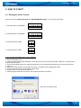
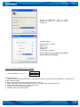
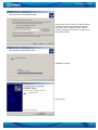
1
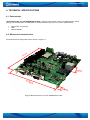
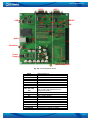
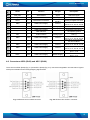
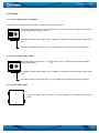
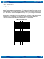
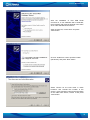
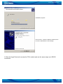
Development KIT for TM1
GSM/GPRS module
User’s Manual v1.1
User’s Manual v1.1
TABLE OF CONTENTS
1. Basic Safety Requirements...................................................................................................................................................... 4
2. General Information................................................................................................................................................................ 5
2.1. INTRODUCTION .................................................................................................................................... 5
2.2. ABOUT THIS DOCUMENT ...................................................................................................................... 5
2.3. LEGAL NOTICE..................................................................................................................................... 5
2.4. CONTACTS........................................................................................................................................... 5
2.5. ACRONYMS ......................................................................................................................................... 5
3. Package Contents..................................................................................................................................................................... 6
4. Technical Specifications .......................................................................................................................................................... 7
4.1. DATA TRANSFER ................................................................................................................................. 7
4.2. MECHANICAL CHARACTERISTICS ........................................................................................................ 7
4.3. SWITCHES............................................................................................................................................ 9
4.4. JUMPERS............................................................................................................................................ 12
4.5. CONNECTOR - JP14 ........................................................................................................................... 13
4.6. CONNECTORS ASC0 (BL09) AND ASC1 (BL09) .............................................................................. 15
4.7. OUTLETS ........................................................................................................................................... 16
4.8. BUTTONS ........................................................................................................................................... 17
4.9. AUDIO ............................................................................................................................................... 17
5. ESD Protection....................................................................................................................................................................... 18
5.1. ESD BASICS ...................................................................................................................................... 18
6. How to Start? ......................................................................................................................................................................... 19
6.1. SETTING THE DEVICE TO WORK ......................................................................................................... 19
6.2. AT COMMANDS EXAMPLES ............................................................................................................... 25
7. Technical Support.................................................................................................................................................................. 27
TROUBLESHOOTING ................................................................................................................................. 27
FINAL NOTICE .......................................................................................................................................... 27
2
User’s Manual v1.1
Attention!
Do not rip the device. Do not touch the device if its block is broken or its connecting wires are
without isolation.
All wireless devices for data transferring may be susceptible to interference, which could affect
performance.
Only qualified personnel may install or repair this product.
Use only in normal projected position. Don't touch the antenna if not necessary.
Pay attention that the device is connected to ~220V supply network.
Your device is not water resistant. Keep it dry.
Do not mount or serve device during a thunderbolt.
3
User’s Manual v1.1
1. BASIC SAFETY REQUIREMENTS
In this document you will be introduced to how to use the “Development KIT for TM1 GSM/GPRS module”
device safely. You will avoid dangerous situations and will not harm yourself if you will follow these
recommendations. You have to be familiar with the safety requirements before starting to use the device!
To avoid burning and voltage caused traumas of the personnel working with device please follow these safety
requirements.
Only a qualified personnel or a person who has enough knowledge about this device and safety
requirements can perform installation and technical support of the device.
The device requires 9V
power supply. The PC to which the device “Development KIT for TM1 GSM/GPRS
module” will be connected must have RS232 or USB port compatible with USB 1.1/2.0 standards. Nominal power
supply voltage is 9V
. Used power supply source should range from 6V...15V
, power up to 300 mW.
The PC and power supply source to which the device “Development KIT for TM1 GSM/GPRS
module” is connected should satisfy LST EN 60950 standard. The device can be used on first
(Personal Computer) or second (Notebook) computer safety class.
To avoid mechanical damage of the device it is recommended to transport the device packed in damage-proof
pack. While using the device it should be placed so that its indication diodes would be visible as they inform in
which working mode the device is and if it has any working problems.
In the installation place and supply circuits should be tool up protective devices (bipolar release device) which will
protect the device from short-circuit and wrong ground installation. The power of connected device should satisfy
the power of released device. The interstice between contacts should not be less than 3 mm. Power supply
network should be installed near device in well accessible place.
If the device starts to work insufficiently only qualified personnel may repair this product. We recommend to
dismantle the device and send it to repair centre or to manufacturers. No exchangeable parts inside of the device.
4
User’s Manual v1.1
2. GENERAL INFORMATION
2.1. Introduction
“Development KIT for TM1 GSM/GPRS module” is a device designed for testing TM1 module features and
functionality. The design of this board enables the connection to your PC via RS232 or USB interface. Once the
board is connected to the PC, you can get access to the TM1 module. Using AT commands you can test its
functionality, such as write SMS, perform calls or even send DATA through GPRS.
2.2. About this document
This document describes “Development KIT for TM1 GSM/GPRS module” hardware, quick guide, plug-in and
operation. It should help users to deploy the product.
2.3. Legal notice
Copyright © 2008 UAB „Teltonika“. All rights reserved.
Reproduction, transfer, distribution or storage of part or all of the contents in this document in any form without the
prior written permission of “Teltonika” is prohibited.
Other product and company names mentioned herein may be trademarks or trade names of their respective
owners.
2.4. Contacts
If you encounter any problems when using our products and cannot solve them by yourself, please contact our
technical support by writing e-mail to [email protected]. We will be glad to help you.
2.5. Acronyms
GPRS
SIM
USB
SMS
GSM
CSD
General Packet Ratio Service
Subscriber Identity Module
Universal Serial Bus
Short Message Service
Global System for Mobile communications
Circuit Switched Data
5
User’s Manual v1.1
3. PACKAGE CONTENTS
“Development KIT for TM1 GSM/GPRS module” is packed in carton box and contains all accessories needed for
normal operation:
1.
2.
3.
4.
5.
6.
7.
8.
9.
Carton box
CD with User’s guide, schematics and software
Development KIT for TM1 GSM/GPRS module device
2xTM1 GSM/GPRS module device
External GSM antenna
Serial cable
USB A ↔ mini USB B cable
Hands free set
AC/DC adapter
Note: the manufacturer does not provide SIM card, which is necessary for connecting to the GSM
network! SIM card can be obtained from your GSM operator!
If any of the components is missing from your package, please contact manufacturer’s representative or reseller
(www.teltonika.lt).
6
User’s Manual v1.1
4. TECHNICAL SPECIFICATIONS
4.1. Data transfer
“Development KIT for TM1 GSM/GPRS module” supports below written carriers of GSM Network. Which
data type is used depends on GSM operator and data transfer capacity in the chosen GSM Network.
GPRS class 10 (class B)
CSD
SMS (text/data)
4.2. Mechanical characteristics
Device dimensions and general view is shown in Figure 4.1.
m
5m
3
1
Fig. 4.1 Development KIT for TM1 GSM/GPRS module
7
User’s Manual v1.1
ASC0
JP13
ASC1
JP12
USB
SW3
JP5
SW5
SW4
RESET
ON
SW1
JP10
JP7
JP1
JP2
JP3
Audio
JP14
JP4
Handsfree
JP9
JP11
Power
Supply
JP6
JP8
VBAT VCHARGE
Fig. 4.2 TM1 development board
ASC0
ASC1
USB
Power Supply
Audio
Handsfree
SW1,SW5
SW3, SW4
JP1, JP2, JP3,
JP4
JP5
JP6
JP7
JP8, JP11
JP9
JP10
JP12, JP13
JP14
VBAT
VCHARGE
Serial interface 0
Serial interface 1
USB interface
Power Supply +9V
Configurable Audio interface
Audio interface for handsfree set
Serial interface control switches
USB interface control switches
Audio configuration jumpers, please
refer to TM1 User manual for more
detailed information.
Power ON button control
Connects VBAT with VCHARGE
ADC1 control jumper
Board power jumpers
Ground
I2C/SPI interface selection
Serial interface enable/disable jumpers
60 pin connector
Connection of external battery
Connection of charger for battery
8
User’s Manual v1.1
4.3. Switches
Switch – SW5
1 (RXD_1) Receiving data (ON/OFF). If switch 1 is ON, then TM1 module
asynchronous serial interface input port is connected to peripheral devices
through RS232 (ASC1). Otherwise, it is disconnected.
2 (TXD_1) Transmitting data (ON/OFF). If switch 2 is ON, then TM1 module
asynchronous serial interface output port is connected to peripheral devices
through RS232 (ASC1). Otherwise, it is disconnected.
3 (CTS_1) Clear to send (ON/OFF). If switch 3 is ON, then TM1 module clear
to send port input is connected to peripheral devices through RS232 (ASC1).
Otherwise, it is disconnected.
4 (RTS_1) Request to send to TM1 module (ON/OFF). If switch 4 is (ON),
then data transmit request to TM1 module output port is connected to
peripheral devices through RS232 (ASC1). Otherwise, it is disconnected
9
User’s Manual v1.1
Switch – SW3
1 (RXD) Receiving serial data (ON/OFF). If switch 1 is ON, then TM1
module receiving serial data output is connected to peripheral devices
through USB port. Otherwise, it is disconnected.
2 (TXD) Transmitting serial data (ON/OFF). If switch 2 is ON, then
TM1 module transmitting serial data output is connected to peripheral
devices through USB port. Otherwise, it is disconnected.
3 (CTS) Clear to send (ON/OFF). If switch 3 is ON, then TM1 module
clear to send port input is connected to peripheral devices through
USB port. Otherwise, it is disconnected.
4 (RTS) Request to send to TM1 module (ON/OFF). If switch 4 is
(ON), then data transmit request to TM1 module output port is
connected to peripheral devices through USB port. Otherwise, it is
disconnected.
5 (DTR) Data terminal ready (ON/OFF). If switch 5 is ON, then TM1
module asynchronous serial interface input port is connected to
peripheral devices through USB port. Otherwise, it is disconnected.
6 (DSR) Data set ready (ON/OFF). If switch 6 is (ON), then peripheral
devices are connected to jumper JP4 pin through USB port.
Otherwise, it is disconnected.
7 (DCD) Data carrier detect (ON/OFF). If switch 7 is ON, then TM1
module asynchronous serial interface output port is connected to
peripheral devices through USB port. Otherwise, it is disconnected.
8 (RI) Ring indicator (ON/OFF). If switch 8 is ON, then TM1 module
ring indicator output port is connected to peripheral devices through
and USB ports. Otherwise, it is disconnected.
10
User’s Manual v1.1
Switch – SW4
1 (RXD_1) Receiving serial data (ON/OFF). If switch 1 is ON, then
TM1 module receiving serial data output is connected to peripheral
devices through USB port. Otherwise, it is disconnected.
2 (TXD_1) Transmitting serial data (ON/OFF). If switch 2 is ON, then
TM1 module transmitting serial data output is connected to peripheral
devices through USB port. Otherwise, it is disconnected.
3 (CTS_1) Clear to send (ON/OFF). If switch 3 is ON, then TM1
module clear to send port input is connected to peripheral devices
through USB port. Otherwise, it is disconnected.
4 (RTS_1) Request to send to TM1 module (ON/OFF). If switch 4 is
(ON), then data transmit request to TM1 module output port is
connected to peripheral devices through USB port. Otherwise, it is
disconnected.
5 (DTR_1) Data terminal ready (ON/OFF). If switch 5 is ON, then TM1
module asynchronous serial interface input port is connected to
peripheral devices through USB port. Otherwise, it is disconnected.
6 (DSR_1) Data set ready (ON/OFF). If switch 6 is (ON), then
peripheral devices are connected to jumper JP4 pin through USB port.
Otherwise, it is disconnected.
7 (DCD_1) Data carrier detect (ON/OFF). If switch 7 is ON, then TM1
module asynchronous serial interface output port is connected to
peripheral devices through USB port. Otherwise, it is disconnected.
8 (RI_1) Ring indicator (ON/OFF). If switch 8 is ON, then TM1 module
ring indicator output port is connected to peripheral devices through
USB ports. Otherwise, it is disconnected.
11
User’s Manual v1.1
4.4. Jumpers
Jumper ports are numbered from left to right. The first jumper port is marked by a square and crossed upper left
corner.
Jumper – JP1
Set JP1 to connect AUDIO interface speaker with AUON
Jumper - JP2
Set JP2 to connect AUDIO interface speaker with MIC
Jumper - JP3
Set JP3 to connect AUDIO interface speaker with AUOP
Jumper - JP4
Set JP4 to connect AUDIO interface speaker with GND
Jumper - JP5
Set J5 to short Power ON button
Jumper – JP6
Set JP6 to connect VBAT and VCHARGE
Jumper – JP7
Set JP7 for setting ADC1 to low level
Jumper - JP8
Set JP8 to connect board power
Jumper - JP9
GND Jumper
12
User’s Manual v1.1
Jumper - JP10
Set 1-2 to select SPI interface.
Set 2-3 to select I2C interface.
Jumper - JP11
Set JP8 to connect board power
Jumper – JP12
Set this pin to disable serial port ASC1.
Jumper – JP13
Set this pin to disable serial port ASC0.
4.5. Connector - JP14
Fig. 4.3 General view of JP14 connector
Table 4.1 Port description of JP14 connector
PIN
#
Name
I/O
Function
I/O type
1
VBAT
PWR
GSM Power Supply
Module Supply
2
VBAT
PWR
GSM Power Supply
Module Supply
3
GND
PWR
GSM Power Supply
Ground
4
VCHARGE
PWR
GSM Power Supply
Module Charge
5
VCHARGE
PWR
GSM Power Supply
Module Charge
6
GND
PWR
GSM Power Supply
Ground
7
KEYOUT0/GPIO
I/O
Keypad interface / GPIO
8
KEYOUT1/GPIO
I/O
Keypad interface / GPIO
9
KEYOUT2/GPIO
I/O
Keypad interface / GPIO
10
KEYOUT3/GPIO
I/O
Keypad interface / GPIO
CMOS
3.3V
compatible
CMOS
3.3V
compatible
CMOS
3.3V
compatible
CMOS
3.3V
Description
Should be connected with
pins 2, 51, 52
Should be connected with
pins 1, 51,52
Should be connected with
pins 6, 17, 42, 45, 47, 49,
50
Should be connected with
pin 5
Should be connected with
pin 4
Should be connected with
pins 3, 17, 42, 45, 47, 49,
50
Keypad output pin 0 / GPIO
00
Keypad output pin 1 / GPIO
01
Keypad output pin 2 / GPIO
02
Keypad output pin 3 / GPIO
13
User’s Manual v1.1
PIN
#
Name
I/O
Function
I/O type
Description
03
Keypad output pin 4 / GPIO
04
Keypad output pin 5 / GPIO
05
Keypad input pin 0 / GPIO
06
Keypad input pin 1 / GPIO
07
Keypad input pin 2 / GPIO
08
Keypad input pin 3
/ GPIO 09
Should be connected with
pins 3, 6, 42, 45, 47, 49, 50
11
KEYOUT4/GPIO
I/O
Keypad interface / GPIO
12
KEYOUT5/GPIO
I/O
Keypad interface / GPIO
13
KEYIN0/GPIO
I/O
Keypad interface / GPIO
14
KEYIN1/GPIO
I/O
Keypad interface / GPIO
15
KEYIN2 / GPIO
I/O
Keypad interface / GPIO
16
KEYIN3/GPIO
I/O
Keypad interface /
GPIO
compatible
CMOS
3.3V
compatible
CMOS
3.3V
compatible
CMOS
3.3V
compatible
CMOS
3.3V
compatible
CMOS
3.3V
compatible
CMOS 3.3V
compatible
17
GND
PWR
GSM Power Supply
Ground
18
CAP00_EX5IN/GPIO
I
External Interrupt
I
Power on
Asynchronous
Serial Interface 0
Asynchronous
Serial Interface 0
Asynchronous
Serial Interface 0
Asynchronous
Serial Interface 0
Asynchronous
Serial Interface 0
Asynchronous
Serial Interface 0
Asynchronous
Serial Interface 0
Asynchronous
Serial Interface 0
Generic digital
signal
Generic digital
signal
Generic digital
signal
Generic digital
signal
Generic digital
signal
Generic digital
signal
Generic digital
signal
Generic digital
signal
Generic digital
signal
Generic digital
signal
Generic digital
signal
Generic digital
signal
Generic digital
signal
Digital Audio Interface /
Synchronous Serial Interface
Generic digital
signal
Digital Audio Interface /
Synchronous Serial Interface
Digital Audio Interface /
Synchronous Serial Interface
Generic digital
signal
Generic digital
signal
I
Digital Audio Interface /
Synchronous Serial Interface
Generic digital
signal
SCL
O
I2C bus interface
36
SDA
I/O
I2C bus interface
37
SIM_CLK
O
SIM interface
38
SIM_IO
I/O
SIM interface
19
PWR_ON
20
CAP05/GPIO
I/O
GPIO
21
CAP19_GPIO
I/O
GPIO
22
EXTRSTN
I
External reset
23
DSR
O
24
RI
O
25
DCD
O
26
DTR
I
27
CTS
I
28
RTS
O
29
RXD
I
30
TXD
O
31
WA0_DAI
I/O
32
TXD_DAI
O
33
CLK0_DAI
I/O
34
RXD_DAI
35
Generic digital
signal
Generic digital
signal
SIM interface
signal
SIM interface
signal
Ext Int 5B
Power on button
GPIO 37
GPIO 36
External HW reset
Data Set Ready
Ring Indicator
Data Carrier Detect
Data Terminal Ready
RTS (DCE)
CTS (DCE)
RX (DCE)
TX (DCE)
DAI Reset /
Master Transmit Slave
Receive
DAI Transmit /
SSC chip select
DAI Clock /
Shift Clock
DAI Receive /
Master Receive Slave
Transmit
Serial Clock Line
Serial Data Line
SIM clock signal
SIM I/O serial data
14
User’s Manual v1.1
PIN
#
Name
I/O
Function
39
SIM_RST
O
SIM interface
40
SIM_VCC
PWR
SIM interface
41
ADC1
I
Measurement interface
42
GND
PWR
GSM Power Supply
Ground
43
44
AUOP
AUON
O
O
Analog signal
Analog signal
45
MIC_GND
PWR
Audio Interface
Audio Interface
GSM Power Supply
MIC reference
46
MIC
I
Audio Interface
Analog signal
47
GND
PWR
GSM Power Supply
Ground
48
ANT
RF
GSM antenna
RF
49
GND
PWR
GSM Power Supply
Ground
50
GND
PWR
GSM Power Supply
Ground
51
VBAT
PWR
GSM Power Supply
Module Supply
52
VBAT
PWR
GSM Power Supply
Module Supply
I/O type
SIM interface
signal
SIM Supply
ADC 12bits
0-0.96 V
Ground
Description
SIM reset signal
SIM power supply
Analog to Digital Converter
Should be connected with
pins 3, 6, 17, 45, 47, 49, 50
Balanced power audio out
Balanced power audio out
Should be connected to
microphone ground
Handset microphone
bias (+)
Should be connected with
pins 3, 6, 17, 42, 45, 49, 50
Should be connected with
50 ohm PCB line
Should be connected with
pins 3, 6, 17, 42, 45, 47, 50
Should be connected with
pins 3, 6, 17, 42, 45, 47, 49
Should be connected with
pins 1, 2, 52
Should be connected with
pins 1, 2, 51
4.6. Connectors ASC0 (BL09) and ASC1 (BL09)
There are two ASC0 (BL09) (Fig. 4.4) and ASC1 (BL09) (Fig. 4.5) connectors integrated in the test board. Figures
show port numeration and incoming/outgoing signal names.
Fig. 4.4 General view of ASC0 connector
Fig. 4.5 General view of ASC1 connector
15
User’s Manual v1.1
4.7. Outlets
4.7.1. Power supply outlet - VCHARGE
Outlet ports are numbered from left to right. A square port marks the first port.
The power supply provides 0 - 12V
the VCHARGE power supply outlet.
(nominal: 6V), 300 mA current. Voltage is connected to
1 Negative voltage power supply wire (-) (GND) is connected to the first power supply outlet
port.
2 Positive voltage power supply wire (+) is connected to the second power supply outlet port.
4.7.2. Power supply outlet - VBAT
The power supply provides 3.5 - 4.2 V
power supply outlet.
(Typical: 3.8 V). Voltage is connected to the VBAT
1 Negative voltage power supply wire (-) (GND) is connected to the first power supply outlet
port.
2 Positive voltage power supply wire (+) is connected to the second power supply outlet port.
4.7.3. Power supply outlet
The power supply, which provides 6 - 15V DC voltage, is connected to power supply
outlet.
16
User’s Manual v1.1
4.8. Buttons
4.8.1. Button “RESET”
Button “RESET” is useful to reset TM1 module.
4.8.2. Button “ON”
Button “ON” is a TM1 module power ON button. To turn TM1 module ON, push “ON” button and hold it for
approximately 2 seconds. To check the module status – send an AT command. If TM1 module replies, then it is
ON.
4.9. Audio
4.9.1. Audio 1
Port description:
1 – Handset microphone reference
2 – Balanced power audio out
3 – Balanced power audio out
4 – Handset microphone bias
4.9.2. Handsfree
2
1
Port description:
1 – AUON – Balanced power audio out
2 – AUOP – Balanced power audio out
3 – GND – Ground
4 – MIC – Handset microphone reference
5 – MIC – Handset microphone bias
3
4
5
1
17
User’s Manual v1.1
5. ESD PROTECTION
5.1. ESD Basics
Normal day-to-day activities can cause people to build up static electricity, which might later be transferred to
objects like electronic devices. An electrostatic discharge (ESD) is the transfer of energy between two bodies
(dissimilar materials) at different electrostatic potentials, either through contact or via an ionized ambient discharge
(a spark). ESD in this context is a high-voltage transient with fast rise time and fast decay time. Several thousand
volts of ESD with a high rise time could break through the junction layer of protective devices easily and cause
damage. The ESD can cause IC failure during the manufacturing, the testing, the handling and the assembly of
ICs.
To help reduce losses due to ESD, ESD protection diodes can be used. ESD protection diodes are designed to
absorb ESD energy that is introduced from I/O ports and travels through the connector onto the system board. ESD
protection diodes thus provide protection against ESD induced system malfunction and/or damage to ICs.
In the Table 5.1 pins which require ESD protection (in case that they will be used) are shown.
Table 5.1 Pins for ESD protection
Name
PIN #
Name
PIN #
VBAT
VBAT
VCHARGE
VCHARGE
KEYOUT0
KEYOUT1
KEYOUT2
KEYOUT3
KEYOUT4
KEYOUT5
KEYIN0
KEYIN1
KEYIN2
KEYIN3
CAP00_EX5IN
PWR_ON
1
2
4
5
7
8
9
10
11
12
13
14
15
16
18
19
20
21
22
23
24
25
DTR
CTS
RTS
RXD
TXD
WA0_DAI
TXD_DAI
CLK0_DAI
RXD_DAI
SCL
SDA
SIM_CLK
SIM_IO
SIM_RST
SIM_VCC
ADC1
AUOP
AUON
GND
MIC
VBAT
VBAT
26
27
28
29
30
31
32
33
34
35
36
37
38
39
40
41
43
44
45
46
51
52
CAP05
CAP19
EXTRSTN
DSR
RI
DCD
18
User’s Manual v1.1
6. HOW TO START?
6.1. Setting the device to work
Before connecting “Development KIT for TM1 GSM/GPRS module” to PC, perform next steps:
ON
DIP
1. Set switch SW3 to 00000000
1 2 3 4 5 6 7 8
ON
DIP
2. Set switch SW4 to 00000000
1 2 3 4 5 6 7 8
3. Set switch SW5 to 0000
ON
DIP
1 2 3 4
ON
DIP
4. Set switch SW1 to 0000
1 2 3 4
If you are using the RS232 port on your computer:
1. Do not set jumper JP13.
2. Insert the SIM card into SIM cardholder. Follow the instructions on the device sticker. Make sure, the SIM card is
pushed inside till it fixes.
3. Connect the RS232 cable to the ASC0 serial interface on the development board and into an empty serial port
on your PC.
4. Plug in the GSM Antenna into the SMA connector on the side of the development board.
5. Connect the power supply to the power supply outlet.
6. If jumper JP5 is not set, press ON button.
7. Start the HyperTerminal to access the TM1 module and follow next steps:
Enter any connection name
19
User’s Manual v1.1
Choose communication port to which
development board is connected (COM1,
COM2, etc.)
Set these settings:
Bits per second = 115200
Data bits = 8
Parity = None
Stop bits = 1
Flow control = Hardware
If flow control is set to None, then module
will not wake up immediately
If you are using the USB port on your computer:
ON
DIP
1. Set switch SW3 to 11111111.
1 2 3 4 5 6 7 8
2. Set jumper JP13.
3. Insert the SIM card into SIM cardholder. Follow the instructions on the device sticker. Make sure, the SIM card is
pushed inside till it fixes.
4. Plug in USB cable to the development board ant to your PC.
5. Plug in the GSM Antenna into the SMA connector on the side of the development board.
6. Connect the power supply to the power supply outlet.
7. If jumper JP5 is not set, press ON button.
8. Install the drivers by following steps:
20
User’s Manual v1.1
The user can install the USB driver only if he
(she) is the administrator of the PC. After the
insertion of the administration password the
following window will be displayed:
In this window choose “No, not this time” and
press “Next” button
In this window choose “Install from a list or
specific location (Advanced)” and press “Next”
button
21
User’s Manual v1.1
In this window select “Search for the best driver
in these locations” and “Include this location in
the search”. Press “Browse” button and find
location of the folder with drivers, choose it and
press “Next” button.
Installation progress
Press “Finish”
22
User’s Manual v1.1
After the installation of TM1 USB Serial
Converter A, a new hardware will be detected;
the procedure that must be followed is the same
as for TM1 USB Serial Converter A.
Again choose “No, not this time” and press
“Next” button
Choose “Install from a list or specific location
(Advanced)” and press “Next” button
Select “Search for the best driver in these
locations” and “Include this location in the
search”. Press “Browse” button and find location
of the folder with drivers, choose it and press
“Next” button.
23
User’s Manual v1.1
Installation progress
Press “Finish”. It will be needed to restart the PC
in order to take affect the new settings.
9. Start the HyperTerminal to access the TM1 module and use the same steps as in RS232
connection.
24
User’s Manual v1.1
6.2. AT Commands examples
6.2.1. Registering on the network
AT
OK
AT+CPIN?
+CPIN: READY
or
+CPIN: SIM PIN
Check PIN status
When CPIN: READY you don’t need to write PIN number.
When CPIN: SIM PIN, please use next command to write PIN
number.
AT+CPIN=”xxxx”
Insert the PIN number xxxx ()
To check PIN type “AT+CPIN?”
OK
AT+COPS=0
OK
AT+CREG?
+CREG: 0, 1
OK
Register the phone on the network
Verify registration
AT+CSQ
+CSQ: 15,95
OK
Check signal intensity
AT+COPS?
+COPS: 0, 0, “ OPERATOR”
OK
Read operator name
6.2.2. Incoming and outgoing calls
ATD(telephone number);
After ATD write telephone number without brackets, at the end
of the command there must be semicolon.
OK
ATH
OK
Hang up
AT+CLIP=1
OK
Activation of caller line ID
RING
RING
RING
Incoming Call
ATA
OK
Answer to Voice Call
ATH
OK
Hang up
25
User’s Manual v1.1
6.2.3. Incoming and outgoing SMS
AT+CMGS=”Telephone number”
>SMS text massage 12345<CTRL+Z>
+CMGS:0
OK
Enter to the text mode
AT+CMGL
+CMGL:302,”REC UNREAD”, ”Telephone
number”,,”06/10/19, 15:45:25+08”
SMS text massage 12345
List all incoming SMS
26
User’s Manual v1.1
7. TECHNICAL SUPPORT
Troubleshooting
Problem
TM1 module is not answering after
approximately 23 s.
TM1 module is not responding to AT
commands
Solution
This means that Flow Control is set to NONE. Set Flow
Control to Hardware (RTS/CTS), in other case module
will response only after pressing “RESET” button.
Check module power jumper. It must be set.
Final notice
The label on the package indicates that before using the product the User’s Guide
contained in the package must be read and understood.
The label on the package indicates that used electronic and electric equipment should
be disposed separately.
If you encounter any problems while using the device and you are not able to solve them yourself, then you are
always welcome to contact our technical support department by e-mail [email protected]. We will be glad to
help you.
27