1
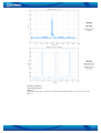
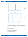
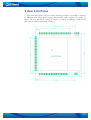
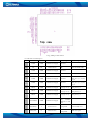
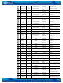
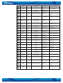
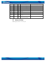
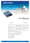
User Manual
TM2Q GSM/GPRS Module
History
Company was established on 15th of
April 1998. Main residence is based in
Vilnius.
ompany started with production of
telecommunication devices.
In 2001 company expanded its fields of
activity
by starting
design
and
manufacturing of electronical systems
for wireless data transfer.
In 2002 contract of partnership and
collaboration was signed with company
Pro-Sign GmbH (Germany), considering
design and representation of graphic
programming interface iCon-L in Eastern
Europe.
In 2003 Teltonika and NOKIA became
partners and started integration of
NOKIA M2M technology using NOKIA
N12 module. It was the beginning of
wireless technology development process.
In 2004, NOKIA invited Teltonika to
join presentation of M2M technology
innovations in CeBIT 2004. It was very
high evaluation of a small Lithuanian
company and its possibilities, which
helped
to
feel peculiarities
of
international business.
About US
In 2004 Teltonika produced more than
10 new products and solutions using
EDGE technology. It was a condition
that made Teltonika a leader of M2M
integration solutions using EDGE not
only in Lithuania, but also in Europe.
2005 was the year of two successful
international exhibitions: CEBIT 2005
and HANNOVER MESSE 2005. These
shows opened new possibilities for
offering our products and solutions for
all world.
In the year 2005 Teltonika became an
international company. We became
Lithuanian - Finnish Company. A few
employees from NOKIA joined
Teltonika’s staff. Presently they
successfully develop activity of new
companies: Teltonika International
GmbH (Düsseldorf) and Teltonika
International Oy (Helsinki).
Our vision is to provide added value for
people
and
companies by
creating electronical
devices
and
solutions, which are based on the latest
achievements of science and technology.
We aim to help people to integrate the
latest technologies in real life, what
would bring more cosiness, comfort,
freedom of mobility and security to their
everyday life.
We seek to make all our solutions an
inconceivable part of people lives.
Table of Contents
1 Document Mission
1.1
Glossary
1.2
Scope of Product
1.3
Power Management
1.4
Interface
1.5
Miscellaneous features
2 Product functions
2.1
System Features
2.2
Modem
2.2.1 Mechanical characteristics
2.2.2 Power supply
2.2.2.1 Current consumptions
2.2.2.2 Power Saving
2.2.3 GSM/GPRS modem functionalities
2.2.4 Supplementary servines
2.2.5 Short Message Service
2.2.6 SIM Functionality
2.2.7 AT-command support
2.2.8 Other basic features
3 User Interfaces
3.1
SIM Interface
3.2
Battery
3.3
Antenna interface
3.4
Asynchronous Serial interface
3.5
GPIO
3.6
SW interfaces
3.7
Audio devices
3.7.1 Handset
3.7.2 Headset
3.7.3 Microphone
3.7.4 Hands-free
3.7.5 Polyphonic ringer
3.7.6 ADC interface / Measurement interface
3.7.7 SPI
3.7.8 I2C bus interface
3
3
5
5
6
6
7
7
10
11
11
12
14
15
16
16
16
16
16
18
22
22
23
24
24
25
30
30
30
30
30
30
31
31
31
2
1 Document Mission
The TM2Q User Manual provides all information necessary for a successful
integration of TM2Q module into the application of the customer. Additionally,
TM2Q User Manual contains all product functions for application.
1.1
Glossary
Abbreviation
/ Term
ADC
Explanation / Definition
Analog-to-Digital Converter
ADN
AFC
AND
AMR
Abbreviated Dialling Numbers
Automatic Frequency Correction
Abbreviated Dialing Number
Adaptive Multi Rate
API
ASC
BCCH
Application Programming Interface
Asynchronous Serial Interface Controller
Broadcast Control Channel
BDN
CB
CBCH
CCCH
Barred Dialing Number
Cell Broadcast
Cell Broadcast Channel
Common Control Channel
CD
CGU
CLI
CSD
Carrier Detect
Clock Generation Unit
Calling Line Identifcation
Circuit Switched Data
DAI
DCE
Digital Audio Interface
Data Communication Equipment
DCS
DCXO
Digital Cellular System (1800 MHz)
Digital Controlled Crystal Oscillator
DL
DSP
DSR
DTE
DTMF
Reception
Digital Signal Processor
Data Set Ready
Data Terminal Equipment
Dual Tone Multi Frequency
DTR
EBU
EFR
Data Transmit Receive
External Bus Interface Unit
Enhanced Full Rate
EGSM
Extended - Global System for Mobile Communication
3
EMS
ESD
ETSI
Enhanced Messaging Service
Electro Static Discharge
European Telecommunications Standards Institute
FDN
FFS
FR
GPIO
Fixed Dialing Number
Flash File System
Full Rate
General Purpose Input/Output
GPP
GPRS
GSM
3rd Generation Partnership Project
General Packet Radio System
Global System for Mobile Communication
HR
Half Rate
HW
Hardware
IC
Integrated Circuit
I2C
Inter-Integrated Circuit
IIR
Infinite Impulsive Response
IMEI
International Mobile Equipment Identity
JTAG
Joint Test Action Group
LDN
M2M
ME
MIDI
Last Dialing Number
Machine-to-Machine
Mobile Equipment
Musical Instrument Digital Interface
MS
MSC
N-AMR
NOM
Mobile Station
Multi-Slot Class
Narrow-AMR
Network Operating Mode
NV
PA
PC
PBCCH
PCCCH
Non Volatile
Power Amplifier
Personal Computer
Packet Broadcast Control Channel
Packet Common Control Channel
PCS
PDP
PDU
Personal Communication Service
Packet Data Protocol
PLMN
PPS
PST
PWM
RF
RTC
RX
Protocol Data Unit
Public Land Mobile Network
Protocol and Parameter Selection
Protocol Stack
Pulse Width Modulation
Radio Frequency
Real Time Clock
Receiver
4
SAW
Surface Acoustic(al) Wave
SDN
SIM
SMA
SMS
Service Dialing Number
Subscriber Identity Module
SubMiniature version A connector
Short Message Service
SMS MO
SMS MT
SPMidi
SPI
SSC
STK
SW
TCH
TX
UART
UL
1.2
Short Message Service Mobile-Originated
Short Message Service Mobile-Terminated
Scalable Polyphony MIDI
Serial Peripheral Interface
Serial Synchronous Interface Controller
SIM Toolkit
Software
Traffic Channel
Transmitter
Universal Asynchronous Receiver-Transmitter
Transmission
Scope of Product
TM2Q is a small, light weight and low power consumption module that enables
digital communications services on GSM/GPRS networks for machine to machine or
user to machine wireless applications.
TM2Q modules are developed in compliance with internal and normative
certification requirements. In particular, they are certified by CE approval report and
Radio & Tele Terminal Equipment Directive (R&TTED) report. Requirements for
lead-free components are imposed and satisfied.
The product implements a quad-band MS able to operate in the frequency bands
GSM 850 MHz, EGSM 900 MHz, and DCS 1800 MHz and PCS 1900 MHz; the
dynamic behavior can be configured dynamically by disabling/enabling a specific band
e.g. through AT commands. Eventually, the module can be configured either dualband or tri-band or quad-band.
The supported power classes for both voice and data services will be:
Class 4 (2W) for GSM/EGSM bands.
Class 1 (1W) for DCS/PCS bands.
The product implements a Class B Mobile Station; this means the data module can
be attached to both GPRS and GSM services, using one service at a time. Network
operation modes I to III are supported, with user-definable preferred service between
GSM and GPRS.
Ignition: it takes around 800 ms to enter in AT active state (eg AT OK, see
picture). From this state we have a 2 seconds setup and stabilization time before the
startup signal is sent to the m2m applications.
Minimum RESET time safe value is 120 ms
1.3
Power Management
Battery connector.
5
1.4
Interface
1.5
63 pin Surface mouting interface: Audio (2x analog, 1x digital), I2C bus,
SPI bus, 2x ADC, 2x analog out (PWM), 12 GPIOs.
2 UART serial ports.
Miscellaneous features
40 tones polyphonic ring tones support.
6
2 Product functions
2.1
System Features
A comprehensive list of TM2Q’s features is presented in the following table and
further detailed in the following paragraphs. The features can be shared in the
following sections:
Generic features;
GSM/GPRS modem functionalities;
Mechanical and Electronics features;
Software features;
Accessory support ;
Host SW tools.
Set of features
Type approval
Environmental constraints
Description
CE approval report available
Radio & Tele Terminal Equipment Directive (R&TTED)
report available
Requirements for lead-free components
Platform security concept description available
Security
Secure IMEI management
Secure flashing environment
Secure memory area
Software update
Software update using system connector
Module testing SW
Service software API
functionality
Rewrite IMEI
Manage SIM locks
Backup and restore user data
Defect logger to analyze memory trace
GSM standard compliancy
ETSI GSM Phase 2+ (R99)
GSM 850 MHz
EGSM 900 MHz
Frequency Bands
DCS 1800 MHz
PCS 1900 MHz
Disable band/Manual band selection
GPRS multi-slot class (MSC) 10 (4+1, 3+2)
GPRS PBCCH/PCCCH support
GSM/GPRS Data Services
CBCH reception when on PBCCH supported
GPRS Class B and CC
Coding scheme CS-1, CS-2, CS-3, CS-4
Network operation mode I, II, III
7
Set of features
Description
CSD up to 9.6kbps (V.32, V.110)
FAX G3, Class 2.0
Short Message Service Mobile-Terminated (SMS MT)
Short Message Service Mobile-Originated (SMS MO)
SMS Short message service
SMS-CB Cell Broadcast (SMS CB)
Concatenated SMS
Via GSM or GPRS
Text and PDU mode
Abbreviated Dialling Numbers (ADN)
Fixed Dialling Numbers (FDN)
SIM Functionality
Last Dialled Numbers (LDN)
Service Dialling Numbers (SDN)
SIM Lock protection
SIM Toolkit
Network
Network subset
SIM Locks
Service provider
Corporate
Operator
Display of Called Number
Indication of Call Progress Signals
Country/PLMN Indication
Short Message Indication and Acknowledgement
Basic Mobile Station features
International Access Function
Service Indicator
Dual Tone Multi Frequency (DTMF)
Subscription Identity Management
On/Off Switch
Service Provider Indication
Call Hold (CH)
Call Waiting (CW)
Multi-Party (MTPY)
GSM Supplementary services
Call Forwarding (CF)
Explicit Call Transfer (ECT)
Call Barring (CB)
Calling Line Identification Presentation (CLIP)
Calling Line Identification Restriction (CLIR)
8
Set of features
Description
Connected Line Identification Presentation (COLP)
Connected Line Identification Restriction (COLR)
Unstructured Supplementary Services Data (USSD)
Audio Codecs
Speech codecs FR (Full rate) / EFR (Enhanced Full Rate) /
HR (Half Rate)
Speech codecs AMR (Adaptive Multi Rate)
Encryption algorithms
Mechanical features
Encryption algorithms A5/1
Encryption algorithms A5/2
Number of RF shield required = 1
Number of PIN's used for SW flashing = 3 (RX/TX and
Ground)
Connector
RTC
Surface mouting
Real Time Clock (RTC) supported with alarm capabilities
SIM voltage: 1.8 and 3 V
SIM
High-speed interface
External SIM ESD protection required.
External SIM connector support
Protection circuitry integrated on the platform
Battery
Charging of deeply discharged battery must be possible.
Charging during phone call
Maximum charging current of battery :1100 mA
Audio features
Audio filter types
supported
Handsfree and headset operation
Echo canceller
Noise reduction
Maximum number of GPIO-interfaces 12
Number of UART's 2
Number of free UART's for user : 1
I/O Interfaces
Power on
One UART with complete 9-pin UART 1
Max speed UART 921.6 Kbps (default AT commands 115.2
kbps)
One UART with only RX/TX
Power on time (sec) 3 sec
9
Set of features
Call Handling
Description
Redial missed and/or received calls (CLI)
Abbreviated Dialling
Full duplex
Call phone
Ringtones
Polyphonic ringtones
HR, FR, EFR, AMR
Audio formats integrated with
the hardware
Accessory support
2.2
MIDI 1.0
iMelody
Number of simultaneous polyphonic tones (without
extra HW) 40
Audio headset
Charger
Modem
The modem part provides with minimal component’s list all functionality
necessary for voice and data transmission over GSM and GPRS network. The modem
is divided in two separated areas surrounded by traces on which metal boxes can be
soldered. The first area encloses the RF High power components and the remaining
passive components of the transceiver; the second area group’s baseband processor,
memory, crystals and power management unit.
10
2.2.1
Mechanical characteristics
The Number of RF shield required is 1. For mechanical characteristics of
GSM/GPRS module refer to the following:
Fig. 2.2.1.1 TM2Q Dimensional layout
Mechanical and environment
Size
Weight
Operating temperature range
2.2.2
Value
33.5 mm x 38.8 mm x 5.6 mm
< 10 g
From -20°C to +55°C
Power supply
The range of VBAT is between 3.5 V and 4.2 V, while typically its value is
3.8V.
Description
Min
Typ
Max
Supply voltage
3.5 V
3.8 V
4.2 V
11
2.2.2.1
Current consumptions
Current consumptions of TM2Q module are reported in the following pages. Power
OFF current is < 30 µA.
BAND: GSM900
TEST SETTINGS:
DRX: 5;
BA LIST arfcn: 1 9 17 26 34 42 50 58 67 75 83 91 99 108 116 124;
PCL: 5.
BAND: GSM1800
TEST SETTINGS:
DRX: 5
BA LIST arfcn: 512 530 560 580 610 640 670 700 720 740 760 790 810 840 860
PCL: 0
12
BAND: GSM1900
TEST SETTINGS:
DRX: 5
BA LIST arfcn: 512 530 550 570 590 610 630 650 670 690 710 730 750 770 790
PCL: 0
13
2.2.2.2
Power Saving
Power saving is a special function that allows the reducing of power
consumption during the idle time. If the clock increases, required power increases too.
Therefore a solution for minimizing the power is the reducing of the master clock
frequency when there aren’t activities. In this period the system doesn’t work with a
clock of 26 MHz (“fast clock”) but with a clock of 32 KHz (RTC clock or “slow
clock”). This switching between 26 MHz and 32 KHz clock is performed by SCCU
(Standby Clock Control Unit).
Main priorities of power saving are the following:
1. Reduce base (min) current consumption.
2. Minimize full-speed running periods, minimize power saving on/off switching.
3. Reduce max current consumption.
These points are reported in the following figure:
14
2.2.3
GSM/GPRS modem functionalities
TM2Q GSM/GPRS module integrates a full-featured R99 GSM-GPRS Protocol
Stack, whose main characteristics are listed in the following. Refer to the Teltonika
PICS/PIXIT documentation for a detailed description of the Stack features.
The module can be configured either dual-band or tri-band or quad-band. The
product implements a quad-band MS able to operate in the frequency bands GSM 850
MHz, EGSM 900 MHz, DCS 1800 MHz and PCS 1900 MHz; the dynamic behavior
can be configured dynamically by disabling/enabling a specific band e.g. through AT
commands. The supported power classes for both voice and data services will be:
Class 4 for GSM band.
Class 1 for DCS bands.
The product implements a Class B Mobile Station; this means the data module can
be attached to both GPRS and GSM services, using one service at a time. Network
operation modes I to III are supported, with user-definable preferred service between
GSM and GPRS. Optionally paging messages for GSM calls can be monitored during
GPRS data transfer in not-coordinating network operation mode NOM II-III.
PBCCH/PCCCH logical channels are supported, as well as CBCH reception. GPRS
multislot 10 is implemented, implying a maximum of 4 slots in DL (reception) and 2
slots in UL (transmission) and 5 slots on the whole. Finally TM2Q GSM/GPRS
module supported:
All coding schemes from CS1 to CS4.
As for the circuit switched services, speech channel modes HR and FR version
1, 2 and 3 (FR, HR, EFR, N-AMR) are supported.
Encryption algorithms A5/1 and A5/2 for GSM for GPRS are supported;
CS Data calls are supported in transparent/non transparent mode up to 9.6
kbps.
Bearer service fax Group 3 Class 2.0 is supported.
Among access interfaces to DTE, both V.32 and V.110 are provided.
15
2.2.4
Supplementary servines
The following supplementary services are provided:
Call Hold (CH).
Call Waiting (CW).
Multi-Party (MTPY).
Call Forwarding (CF).
Explicit Call Transfer (ECT).
Call Barring (CB).
Calling Line Identification Presentation (CLIP).
Calling Line Identification Restriction (CLIR).
Connected Line Identification Presentation (COLP).
Connected Line Identification Restriction (COLR).
Unstructured Supplementary Services Data (USSD).
2.2.5
Short Message Service
Mobile-originated as well as mobile-terminated SMS are supported. Text and PDU
mode are supported. Reception of SMS during circuit-switched calls is supported.
Reception of SMS via GPRS is also supported. SMS SIM storage is provided.
2.2.6
SIM Functionality
Among SIM functionalities, the following services of the SIM are supported:
Abbreviated Dialing Numbers (ADN).
Fixed Dialing Numbers (FDN).
Last Dialed Numbers (LDN).
Service Dialing Numbers (SDN).
ME Personalization (SIM Lock).
ME Personalization handling is a mechanism to tie the ME operation to one
specific SIM card or to a limited range of SIM cards from a given Network Operator
or Service Provider. The ME will only accept the SIM if there is a positive match
between the personalization code group(s) stored in the ME and the code group(s)
belonging to the inserted SIM. The SIM Lock feature supported by TM2Q
GSM/GPRS module enables ME personalization through the following
personalization categories:
Network lock.
Network subset lock.
Service provider lock.
Corporate lock.
Operator lock.
SIM Toolkit R 99 is supported. For a detailed description of the STK features,
refer to the PICS/PIXIT documentation.
2.2.7
AT-command support
The modem functionalities and services are provided through a rich serial ATcommand interface. All supported standard as well as proprietary AT commands are
detailed in the table of SW interface.
2.2.8
Other basic features
Within the scope of the M2M or user interface, the following indications and
functionalities are supported:
Display of Called Number.
16
Indication of Call Progress Signals.
Country/PLMN Indication.
Short Message Indication and Acknowledgement.
International Access Function.
Service Indicator.
Dual Tone Multi Frequency (DTMF).
Subscription Identity Management.
Service Provider Indication.
Abbreviated Dialing.
Power on (external input).
17
3 User Interfaces
PIN OUT description A 63-pin surface mounting interface is provided to interface
of TM2Q module for the power supply, SIM interface, audio interface (2 x analog, 1x
digital), I2C bus, SPI bus, 2 x analog in (ADC), 2 x analog out (PWM), 2 UART serial
ports, and 12 GPIOs (maximum number).
18
3.1 Fig. TM2Q module Pinout
3.1 Table Pin Out Description
PIN
Name
I/O
1
GND
PWR
Function
GSM Power Supply
I/O type
Ground
2
Ant.
RF
GSM antenna
3
GND
PWR
GSM Power Supply
Ground
4
GND
PWR
GSM Power Supply
Ground
5
GND
PWR
GSM Power Supply
Ground
6
VBAT
PWR
GSM Power Supply
7
VBAT
PWR
GSM Power Supply
8
VBAT
PWR
GSM Power Supply
9
VCHARGE
PWR
GSM Power Supply
10
EXTRSTn
I
External reset
11
SIM_RST
O
SIM interface
Description
RF
Sould be connected
with 50 om RF cable
From 3.3 to 4.3
V (Typ: 3.8 V)
From 3.3 to 4.3
V (Typ: 3.8 V)
From 3.3 to 4.3
V (Typ: 3.8 V)
Should be connected
with pins 4, 5, 63,62,
61 ,44
Should be connected
with pins 4, 5, 63,62,
61 ,44
Should be connected
with pins 6,7, 8
Should be connected
with pins 6,7, 8
Should be connected
with pins 6,7, 8
0 - 12V (Typ:
6V)
Current
limited to 600
mA
CMOS
3.3V
compatible
External HW reset
CMOS
3.3V
compatible
SIM reset signal
19
CMOS
3.3V
compatible
Supply 1.8V3.3V
CMOS
3.3V
compatible
CMOS
3.3V
compatible
12
SIM_CLK
O
SIM interface
13
SIM_VCC
I/O
SIM interface
14
SIM_IO
I/O
SIM interface
15
MRST0/GPI
O
I/O
Synchronous Serial
Interface (SPI
compatible)
16
SDA/GPIO
I/O
I2C bus interface
17
SCL/GPIO
O
I2C bus interface
18
SCLK0/GPI
O
I/O
Synchronous Serial
Interface (SPI
compatible)
19
MICP1
I
Audio Interface
Analog
20
MICN1
I
Audio Interface
Analog
21
MICP2
I
Audio Interface
Analog
22
MICN2
I
Audio Interface
Analog
23
KEYIN2/O
N
I/O
Keypad interface /
Power on
CMOS
3.3V
compatible
Keypad interface /
GPIO
Keypad interface /
GPIO
Keypad interface /
GPIO
Keypad interface /
GPIO
Keypad interface /
GPIO
Keypad interface /
GPIO
Keypad interface /
GPIO
Keypad interface /
GPIO
Keypad interface /
GPIO
CMOS
3.3V
compatible
CMOS
3.3V
compatible
CMOS
3.3V
compatible
CMOS
3.3V
compatible
CMOS
3.3V
compatible
CMOS 3.3V
compatible
CMOS
3.3V
compatible
CMOS
3.3V
compatible
CMOS
3.3V
compatible
24
25
26
27
28
29
30
31
32
KEYOUT2/
GPIO
KEYOUT3/
GPIO
KEYOUT4/
GPIO
KEYIN1/G
PIO
KEYIN0/G
PIO
KEYIN3/G
PIO
KEYOUT5/
GPIO
KEYOUT0/
GPIO
KEYOUT1/
GPIO
I/O
I/O
I/O
I/O
I/O
I/O
I/O
I/O
I/O
CMOS
3.3V
compatible
CMOS
3.3V
compatible
CMOS
3.3V
compatible
33
AUON
O
Audio Interface
Analog
34
AUOP
O
Audio Interface
Analog
35
CAP22_EX3
IN/GPIO
I/O
36
CTS_0
I
37
RTS_0
O
38
TXD_0
O
39
RXD_0
I
40
DTR
I
Capture Compare /
GPIO / External
Interrupt
Asynchronous Serial
Interface 0
Asynchronous Serial
Interface 0
Asynchronous Serial
Interface 0
Asynchronous Serial
Interface 0
Asynchronous Serial
Interface 0
CMOS
3.3V
compatible
CMOS
3.3V
compatible
CMOS
3.3V
compatible
CMOS
3.3V
compatible
CMOS
3.3V
compatible
CMOS
3.3V
compatible
SIM clock signal
SIM power supply
SIM I/O serial data
Master Receive Slave
Transmit
Serial Data Line
Serial Clock Line
Shift Clock
Handset microphone
reference
Handset microphone
bias
Handset microphone
reference
Handset microphone
bias
Keypad input pin 2 /
Power on button
/GPIO 07
Keypad output pin 2 /
GPIO 01
Keypad output pin 3 /
GPIO 02
Keypad output pin 4 /
GPIO 03
Keypad input pin 1 /
GPIO 06
Keypad input pin 0 /
GPIO 05
Keypad input pin 3
/ GPIO 08
Keypad output pin 5 /
GPIO 04
Keypad output pin 0 /
GPIO 00
Keypad output pin 1 /
GPIO 50
Balanced power audio
out
Balanced power audio
out
Capture Compare 22
/ GPIO 55 / Ext Int
3
Clear To Send
Request to Send
Transmit Serial Data
Receive Serial Data
Data Terminal Ready
20
41
DCD
O
42
DSR
O
43
RI
O
44
GND
PWR
45
CAP00_EX5
IN/GPIO
I/O
46
MTSR0/GPI
O
I/O
47
48
49
50
WA0_DAI/
GPIO
CLK0_DAI
/GPIO
TXD_DAI/
GPIO
RXD_DAI/
GPIO
I/O
I/O
O
I
51
TXD_1
O
52
RXD_1
I
53
54
55
56
CAP02/GPI
O
CAP05/GPI
O
CAP06/GPI
O
CAP19/GPI
O
I/O
I/O
I/O
I/O
Asynchronous Serial
Interface 0
Asynchronous Serial
Interface 0
Asynchronous Serial
Interface 0
CMOS
3.3V
compatible
CMOS
3.3V
compatible
CMOS
3.3V
compatible
GSM Power Supply
Ground
Capture Compare /
GPIO / External
Interrupt
Synchronous Serial
Interface (SPI
compatible)
Digital Audio
Interface
Digital Audio
Interface
Digital Audio
Interface
Digital Audio
Interface
Asynchronous Serial
Interface 1
Asynchronous Serial
Interface 1
Capture Compare /
GPIO
Capture Compare /
GPIO
Capture Compare /
GPIO
Capture Compare /
GPIO
Measurement
interface
Measurement
interface
CMOS
3.3V
compatible
Data Carrier Detect
Data Set Ready
Ring Indicator
CMOS
3.3V
compatible
Should be connected
with pins 4, 5, 63,62,
61 ,44
Capture Compare 00
/ GPIO 30 / Ext Int
5B
Master Transmit Slave
Receive
CMOS
3.3V
compatible
DAI Reset
CMOS
3.3V
compatible
CMOS
3.3V
compatible
CMOS
3.3V
compatible
CMOS
3.3V
compatible
CMOS
3.3V
compatible
CMOS
3.3V
compatible
CMOS
3.3V
compatible
CMOS
3.3V
compatible
CMOS
3.3V
compatible
ADC 12bits 02.5V
ADC 12bits 02.5V
57
ADC2
I
58
ADC1
I
59
EPPA2A
O
Audio Interface
Analog
60
EPPA1B
O
Audio Interface
Analog
61
GND
PWR
GSM Power Supply
Ground
62
GND
PWR
GSM Power Supply
Ground
63
GND
PWR
GSM Power Supply
Ground
DAI Clock
DAI Transmit
DAI Receive
Transmit Serial Data
Receive Serial Data
Capture Compare 02
/ GPIO 57
Capture Compare 05
/ GPIO 28
Capture Compare 06
/ GPIO 30
Capture Compare 19
/ GPIO 47
Analog to Digital
Converter
Analog to Digital
Converter
Balanced audio out
Balanced audio out
Should be connected
with pins 4, 5, 63,62,
61 ,44
Should be connected
with pins 4, 5, 63,62,
61 ,44
Should be connected
with pins 4, 5, 63,62,
61 ,44
21
3.2 Fig. TM2Q module
3.1
SIM Interface
TM2Q module can be equipped with an external SIM connector. High-speed
SIM/ME interface is implemented. Both 1.8V and 3V SIM type will be supported
(1.8/3V ME); activation and deactivation with automatic voltage switch from 1.8V to
3V are implemented, according to ISO-IEC 78-16-e Specifications. The SIM driver
supports the PPS (Protocol and Parameter Selection) procedure for baud-rate
selection, according to the values proposed by the SIM Card. Clock stop is supported
at both high and low level. Finally, external SIM ESD protection is required.
3.2
Name
PIN #
I/O
I/O type
Description
SIM_VCC
13
I/O
Supply 1.8V 3.3V
SIM Power Supply
SIM_IO
14
I/O
CMOS 3.3V compatible
SIM I/O Serial Data
SIM_CLK
12
O
CMOS 3.3V compatible
SIM Clock Signal
SIM_RST
11
O
CMOS 3.3V compatible
SIM Reset Signal
Battery
The supported type for the battery shall be Li-Ion rechargeable only; default
system will support 650mAh nominal. Protection circuitry is integrated on the module.
The Battery/Charger functionality provides:
• battery charging control, i.e. constant voltage charging and trickling of charging
in order to maintain the full capacity of the battery;
• pulse charge mode, to improve capacity estimation accuracy;
• capacity estimation during charging, no charging, ongoing calls, etc., constantly
considering the different load parameters of the phone;
• Measurements of battery voltage, RF and battery temperature, equipment
status, etc.
Charging of deeply discharged battery as well as charging during phone call is
possible.
The module has a current consumption lower than 3mA during idle mode
reception, lower than 300 mA in connected mode on GSM band and lower than
180mA in connected mode on DCS band (measurements are performed following the
GSM Association Battery Life Measurement Technique Document). The charging
battery range goes from 400 to 1100 mA with a step of 100 mA.
22
Name
PIN #
I/O
I/O type
VBAT
6
PWR
From 3.3 to 4.3 V (Typ: 3.8 V)
VBAT
7
PWR
From 3.3 to 4.3 V (Typ: 3.8 V)
VBAT
8
PWR
From 3.3 to 4.3 V (Typ: 3.8 V)
GND
4
PWR
Ground
GND
5
PWR
Ground
GND
44
PWR
Ground
GND
61
PWR
Ground
GND
62
PWR
Ground
GND
63
PWR
Ground
VCHARGE
9
PWR
From 0 to 12 V (Typ: 6V)
Current limited to 600 mA
3.3
Description
Antenna interface
GMS Signal put direct to the Ant. pin.
23
3.4
Asynchronous Serial interface
Two serial ports (ASC0 UART and ASC1 UART) are supported working at the
selected baud rate (default 115.2 kbps): on ASC0 complete 9 pin serial port is
supported and power saving wakeup is available. This interface is fullyRS232 9-pin
logical compliant and support full HW flow control. Default UART configuration
implies ASC0 devoted to AT interface, ASC1 available for debug/tracing (only
RX/TX lines). These serial interfaces are available complying with V.24 protocol and
the signals are:
• TX Data (TXD_0).
• RX Data (RXD_0).
• Request to Send (RTS_0).
• Clear to Send (CTS_0).
• Data Terminal Ready (DTR).
• Data Set Ready (DSR).
To avoid floating if output pins are high-impedance, use pull-up resistors tied
to GSM_VDD or pull-down resistors tied to GND. The first 6 pin reported in the
table refer at the first serial interface, while the last two refer at the second serial
interface.
DCD
PIN
#
41
DTR
40
CTS_0
36
I
CMOS 3.3V compatible
Clear To Send
RTS_0
37
O
CMOS 3.3V compatible
Request to Send
RXD_0
39
I
CMOS 3.3V compatible
Receive Serial Data
TXD_0
38
O
CMOS 3.3V compatible
Transmit Serial Data
RI
43
O
CMOS 3.3V compatible
Ring Indicator
DSR
42
O
CMOS 3.3V compatible
Data Set Ready
RXD_1
52
I
CMOS 3.3V compatible
Receive Serial Data
TXD_1
51
O
CMOS 3.3V compatible
Transmit Serial Data
Name
3.5
I/O
I/O type
Description
O
CMOS 3.3V compatible
Data Carrier Detect
I
CMOS 3.3V compatible
Data Terminal Ready
Serial interface #
Asynchronous
Serial Interface 0
Asynchronous
Serial Interface 1
GPIO
All General Purpose I/O (GPIOs) shall be initialized to proper direction / output logic level as
soon as possible. If supply is removed from external device, relevant GPIOs should be placed at low
logic level, or decoupled.
Name
PIN #
I/O
I/O type
KEYOUT0/GPIO
31
I/O
CMOS 3.3V compatible
KEYOUT1/GPIO
32
I/O
CMOS 3.3V compatible
KEYOUT3/GPIO
25
I/O
CMOS 3.3V compatible
KEYOUT4/GPIO
26
I/O
CMOS 3.3V compatible
KEYOUT5/GPIO
30
I/O
CMOS 3.3V compatible
KEYIN0/GPIO
28
I/O
CMOS 3.3V compatible
Description
Keypad output pin 0 /
GPIO 00
Keypad output pin 1 /
GPIO 50
Keypad output pin 3 /
GPIO 02
Keypad output pin 4 /
GPIO 03
Keypad output pin 5 /
GPIO 04
Keypad input pin 0 /
GPIO 05
24
KEYIN1/GPIO
27
I/O
CMOS 3.3V compatible
KEYIN3/GPIO
29
I/O
CMOS 3.3V compatible
CAP19/GPIO
56
I/O
CMOS 3.3V compatible
CAP02/GPIO
53
I/O
CMOS 3.3V compatible
CAP05/GPIO
54
I/O
CMOS 3.3V compatible
CAP06/GPIO
55
I/O
CMOS 3.3V compatible
Keypad input pin 1 /
GPIO 06
Keypad input pin 3 /
GPIO 08
Capture Compare 19 /
GPIO 47
Capture Compare 02 /
GPIO 57
Capture Compare 05 /
GPIO 28
Capture Compare 06 /
GPIO 30
Note: The General Purpose I/O is not accessible using AT commands. It could be
accessible from internal M2M resusrses only.
3.6
SW interfaces
The AT-command interface provides the service and the functionalities of
GSM/GPRS modem. It is possible observe the AT commands of TM2Q module in
the following table.
Command description
General Commands
AT+CGMI
Manufacturer identification
AT+CGMM
Request model identification
AT+CGMR
Request revision identification
AT+CGSN
Request product serial number identification
AT+CSCS
Set TE character set
AT+CIMI
Request international mobile subscriber identification
AT+CCID
Card identification
AT+GCAP
Request complete capability list
A/
Repeat last command
Mobile equipment control and status commands
AT+CPAS
Phone activity status
AT+CPWROFF
Switch off the MS
AT+CFUN
Set phone functionality
AT+CBC
Battery charge
AT+CIND
Indicator control
AT+CMER
Mobile termination event reporting
AT+CCLK
Clock
AT+CALA
Alarm
AT+CRSM
Restricted SIM access
AT+CALM
Alert sound mode
AT+CRSL
Ringer sound level
AT+CLVL
Loudspeaker volume level
AT+CMUT
Mute control
AT+CCWE
Call meter maximum event
AT+CSGT
Set greeting text
AT+CALD
Delete alarm
AT+CTZU
Automatic Time Zone Update
AT+CTZR
Time Zone Reporting
Name
25
AT+CLAC
AT+CMEE
AT+CSTA
ATD
ATT
ATP
ATA
ATH
ATM
ATL
AT+CMOD
AT+CHUP
AT+CEER
AT+VTD
AT+VTS
ATDL
ATS0
AT+CNUM
AT+CSQ
AT+COPS
AT+CREG
AT+CPOL
AT+COPN
AT+CPIN
AT+CLCK
AT+CPWD
AT+CPBS
AT+CPBR
AT+CPBF
AT+CPBW
AT+CSMS
AT+CPMS
AT+CMGF
AT+CSAS
AT+CRES
AT+CSDH
AT+CNMI
AT+CMGR
AT+CNMA
AT+CMGL
AT+CMGS
AT+CMGW
AT+CMSS
List all available AT commands
Report mobile termination error
Call control commands
Select type of address
Dial command (full support of modifiers: ;,>,I,G)
Select tone dialing
Select pulse dialing
Call answer
Hook control
Monitor speaker mode
Monitor speaker loudness
Call mode
Hang up call
Extended error report
Tone duration
DTMF and tone generation
Redial last telephone number
Automatic answer
Network service commands
Subscriber number
Signal quality
Operator selection
Network registration
Preferred operator list
Read operator names
Security commands
Enter PIN
Facility lock
Change password
Phonebook commands
Select phonebook memory storage
Read phonebook entries
Find phonebook entries
Write phonebook entry
Short message commands
Select message service
Preferred message storage
Preferred message format
Save settings
Restore settings
Show text mode parameters
New message indication
Read message
New message acknowledgement to ME/TA
List message
Send message
Write message to memory
Send message from storage
26
AT+CSMP
AT+CMGD
AT+CSCA
AT+CSCB
AT+CCFC
AT+CCWA
AT+CLIR
AT+CLIP
AT+COLP
AT+COLR
AT+CAOC
AT+CACM
AT+CAMM
AT+CPUC
AT+CHLD
AT+CTFR
AT+CLCC
AT+CSSN
AT+CUSD
AT+CCUG
AT+CNAP
AT+CBST
AT+FCLASS
AT+CR
AT+CRC
AT+CRLP
AT+FDT
AT+FDR
AT+FIP
AT+FKS
AT+FK
AT+FAA
AT+FAP
AT+FBS
AT+FBO
AT+FBU
AT+FCC
AT+FCQ
AT+FCR
AT+FCS
AT+FCT
AT+FEA
AT+FFC
AT+FHS
AT+FIE
Set text mode parameters
Delete SMS
Service center address
Select cell broadcast message types
Supplementary services commands
Call forwarding
Call waiting
Calling line identification restriction
Calling line identification presentation
Connected line identification presentation
Connected line identification restriction
Advise of charge
Accumulated call meter
Accumulated call meter maximum
Price per unit and currency table
Call related supplementary services
Call deflection
List current list calls
Supplementary service notifications
Unstructured supplementary service data
Closed user group
Calling name presentation
Data commands
Select bearer service type
Service class selection and identification
Service reporting control
Cellular result codes
Radio link protocol
FAX class 2.0 commands
Transmit data
Receive data
Initialize facsimile parameters
Session termination
Session termination
Adaptive answer
Address & polling capabilities
Buffer size
Data bit order
HDLC frame reporting
DS capabilities parameters
Copy quality checking
Capability to receive data
Current session results
DTE phase C response timeout
Phase C received EOL alignment
Format conversion
Call termination status
Procedure interrupt enable
27
AT+FIS
AT+FIT
AT+FLI
AT+FLO
AT+FLP
AT+FMI
AT+FMM
AT+FMR
AT+FMS
AT+FNR
AT+FNS
AT+FND
AT+FPA
AT+FPI
AT+FPP
AT+FPS
AT+FPW
AT+FRQ
AT+FRY
AT+FSA
AT+FSP
ATZ
AT&F
AT&C
AT&D
AT&S
AT&K
AT&W
AT&V
AT&Y
ATI
AT+GMI
AT+GMM
AT+GSN
AT+GMR
AT+ICF
AT+IFC
AT\Q
AT+IPR
ATO
ATS2
ATS3
ATS4
ATS5
ATS6
ATS7
ATS8
ATS10
Current session parameters
Inactivity timeout
Local ID string
Set flow control
Indicate document to poll
Request manufacturer identification
Request model identification
Request revision identification
Minimum phase C speed
Negotiation reporting
Non-standard frame FIF octet string
NSF message data indication
Selective polling address
Local polling ID string
Packet protocol control
Page status
Password parameter
Receive quality thresholds
Error correction mode retry count
Sub Address parameter
Request to poll
V.24 control and V.25ter commands
Reset to default configuration
Set to factory defined configuration
Circuit 109 (CD) behavior
Circuit 108/2 (DTR) behavior
DSR override
Flow control
Store current configuration
Display current configuration
Designate a default reset profile
Request identification information
Request manufacturer identification
Request model identification
Request product serial number identification
Request revision identification
DTE-DCE character framing
DTE-DCE local flow control
Set flow control
Fixed DTE rate
Return to on-line data state
Escape character
Command line termination character
Response formatting character
Command line editing character
Pause before blind dialing
Connection completion timeout
Command dial modifier time
Automatic disconnect delay
28
ATS12
ATE
ATQ
ATV
Escape prompt delay (EPD)
Command echo
Result code suppression
DCE response format
Result code selection and call progress monitoring
ATX
control
Specific AT commands
AT#
Production test command
AT+CGED
GPRS cell environment description
AT+TRACE
Switch on/off trace
AT+XBANDSEL
Select band
AT+XCALLSTAT Set reporting call status
AT+XGENDATA Display generation and SW version
AT+XGCNTRD
Read counters of sent or received GPRS data
AT+XGCNTSET
Set/reset counter of sent or received GPRS data
AT+XHANDSFREE Set hands free mode
AT+XL1SET
Call the L1-specific function
AT+XSIO
Configuration trace and modem (AT) interfaces
AT+NADC
ADC read command
AT+NGPIOC
GPIO select configuration command
AT+NGPIOR
GPIO read command
AT+NGPIOW
GPIO set command
AT+NRNG
Ringer select command
SIM toolkit
AT+STKPRO
SIM-APPL-TK proactive commands
AT+STKTR
SIM-APPL-TK terminal response
AT+STKENV
SIM-APPL-TK envelope
AT+STKPROF
SIM-APPL-TK terminal profile
AT+STKCC
SIM-APPL-TK call control commands
AT+STKCNF
SIM-APPL-TK proactive session status
GPRS AT commands
AT+CGDCONT
Define PDP context
AT+CGEREP
GPRS event reporting
AT+CGQREQ
Quality of service profile (requested)
AT+CGQMIN
Quality of service profile (minimum acceptable)
AT+CGATT
GPRS attach or detach
AT+CGACT
PDP context activate or deactivate
AT+CGDATA
Enter data state
Automatic response to a network request for PDP
AT+CGAUTO
context activation
AT+CGPADDR
Show PDP address
AT+CGCLASS
GPRS mobile station class
AT+CGREG
GPRS network registration status
AT+CGSMS
Select service for MO SMS messages
29
3.7
Audio devices
3.7.1
Handset
A standard handset is supported for normal handset operation on the default audio
path.
3.7.2
Headset
One earpiece headset is supported and may be used for voice during calls. The
audio path switching from handset to headset is automatic when a rising edge is
detected from line CAP22_EX3XIN (Pin 35); the audio path returning to the headset
when line CAP22_EX3XIN (Pin 35) return to 0 level.
3.7.3
Microphone
The uplink path can be switched between the handset and the headset
microphone. The path switching is driven automatically as described above for the
earpiece. The uplink path can be muted.
3.7.4
Hands-free
A true hands-free functionality is implemented using high power loudspeaker, MS
microphone and appropriate DSP algorithms for voice band handling (Echo canceller
and Automatic Gain control). The product is equipped with a power audio amplifier
that can drive an external 8 ohm speaker with 400mW peak. The audio power
amplifier can be used as a voice amplifier for the hands free functionality and as a
melody player amplifier for ringer functionality. The melody player could be the Midi
synthesizer or the tone generator. In order to minimize the clipping of the audio signal,
the polarization voltage can be adapted to the voltage supply (battery voltage). The
audio signal on the loudspeaker is a mono signal.
3.7.5
Polyphonic ringer
Polyphonic ring-tones can be generated by an internal MIDI synthesizer, which
runs at 16 or 32 KHz sample frequency and can sum up to 40 voices at 16 kHz
sampling rate.
The synthesizer output is only mono and cannot be mixed with TCH voice path
(the two are mutually exclusive). To perform in-band alerting during TCH with voice
path open, only Tone Generator can be used. The output samples of the synthesizer
are post processed by two modules:
• High Frequency Shelving Filter: This module is implemented as a first order IIR
Filter, which is mainly used for high frequency boost in audio signals. Its transfer
function can be controlled by 4 filter coefficients.
• Audio Compressor: The audio compressor is a device for manipulating the
dynamic range of mono or stereo audio signals. The audio compressor can be
controlled by 14 configuration parameters. Polyphonic standard format supported.
The MIDI driver can play:
• MIDI files conforming to:
General Midi Level 1.0 with file-format 0 and 1.
General Midi Lite 1.0.
• SPMidi (Scalable Polyphony MIDI) files conforming to:
SPMidi 1.0.
• iMelody files conforming to:
30
3.7.6
iMelody v.1.2 specifications.
ADC interface / Measurement interface
2 inputs for Analog-to-Digital Converter are supported. The resolution of these
converters is of 12-bit with a range of 0-2.5 Volt.
Name
PIN
I/O
I/O type
Description
ADC1
58
I
ADC 12bits 0-2.5V
Analog to Digital Converter
ADC2
57
I
ADC 12bits 0-2.5V
Analog to Digital Converter
3.7.7
SPI
The SPI bus includes a clock signal, and two signals for the transmissions of the
master and the slave.
Name
PIN I/O
MRST0/GPIO
15
I/O
MTSR0/GPIO
46
I/O
SCLK0/GPIO
18
I/O
3.7.8
I/O type
CMOS
compatible
CMOS
compatible
CMOS
compatible
Description
3.3V
3.3V
3.3V
Master Receive Slave Transmit
Master Transmit Slave Receive
Shift Clock
I2C bus interface
The I2C bus interface includes a serial clock and a serial data line.
Name
PIN
I/O
I/O type
Description
SCL/GPIO
17
O
CMOS 3.3V compatible
Serial Clock Line
SDA/GPIO
16
I/O
CMOS 3.3V compatible
Serial Data Line
31