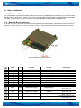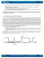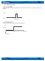
1
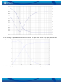
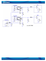
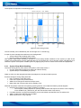
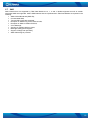
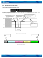
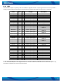
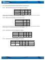
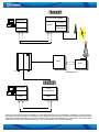
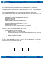
User Manual
TM3 GSM/GPRS/EDGE Module
History
Company was established on 15th of April 1998.
Main residence is based in Vilnius.
ompany
started
with
production
of
telecommunication devices.
In 2001 company expanded its fields of activity
by starting design and manufacturing of electronical
systems for wireless data transfer.
In 2002
contract
of partnership
and
collaboration was signed with company ProSign GmbH (Germany), considering design and
representation of graphic programming interface
iCon-L in Eastern Europe.
In 2003 Teltonika and NOKIA became partners and
started integration of NOKIA M2M technology
using NOKIA N12 module. It was the beginning of
wireless technology development process.
In 2004, NOKIA invited Teltonika to join
presentation of M2M technology innovations in
CeBIT 2004. It was very high evaluation of a small
Lithuanian company and its possibilities, which
helped to feel peculiarities of international business.
About US
In 2004 Teltonika produced more than 10 new
products and solutions using EDGE technology. It
was a condition that made Teltonika a leader of
M2M integration solutions using EDGE not only in
Lithuania, but also in Europe.
2005 was the year of two successful international
exhibitions: CEBIT 2005 and HANNOVER
MESSE 2005. These shows opened new
possibilities for offering our products and
solutions for all world.
In the year 2005 Teltonika became an international
company. We became Lithuanian - Finnish
Company. A few employees from NOKIA joined
Teltonika’s staff. Presently they successfully develop
activity of new companies: Teltonika International
GmbH (Düsseldorf) and Teltonika International Oy
(Helsinki).
Our vision is to provide added value for people and
companies by creating electronical devices and
solutions,
which are
based on
the
latest
achievements of science and technology.
We aim to help people to integrate the latest
technologies in real life, what would bring more
cosiness, comfort, freedom of mobility and security
to their everyday life.
We seek to make all our solutions an inconceivable
part of people lives.
TABLE OF CONTENTS
1
2
3
Document Mission ................................................................................................................................................. 4
Glossary ................................................................................................................................................................. 4
Scope of Product ................................................................................................................................................... 7
3.1
Certification Requirements ............................................................................................................................. 7
4 Product environment.............................................................................................................................................. 8
4.1
Interface.......................................................................................................................................................... 8
5 Product functions ................................................................................................................................................... 8
5.1
Modem............................................................................................................................................................ 8
5.1.1
GSM/EGPRS modem functionalities....................................................................................................... 8
5.1.2
E-GPRS Features.................................................................................................................................... 8
5.1.3
Supplementary services .......................................................................................................................... 9
5.1.4
AT-command support.............................................................................................................................. 9
5.1.5
Other basic features ................................................................................................................................ 9
5.2
Baseband...................................................................................................................................................... 10
5.3
Voiceband..................................................................................................................................................... 10
5.3.1
Audio Power Amplifier ........................................................................................................................... 10
5.3.2
Handset Mode ....................................................................................................................................... 10
5.3.3
Headset Mode ....................................................................................................................................... 10
5.3.4
Microphone............................................................................................................................................ 10
5.3.5
Hands free ............................................................................................................................................. 11
5.3.6
Ringer Mode .......................................................................................................................................... 11
5.3.7
DAI Interface.......................................................................................................................................... 11
5.3.8
Audio Codecs ........................................................................................................................................ 12
5.3.9
Echo canceller/Noise Reduction ........................................................................................................... 12
5.3.10 Circuit Description ................................................................................................................................. 12
5.4
Mechanical characteristics ........................................................................................................................... 15
5.5
Power supply ................................................................................................................................................ 15
5.5.1
Current consumptions ........................................................................................................................... 16
5.6
Power Saving................................................................................................................................................ 16
5.6.1
System Sleep Mode Handling ............................................................................................................... 17
5.7
SMS .............................................................................................................................................................. 18
6 User Interfaces..................................................................................................................................................... 19
6.1
RF Antenna Connector ................................................................................................................................. 19
6.2
Board-to-Board Connector ........................................................................................................................... 19
6.2.1
Switching on of the data module ........................................................................................................... 22
6.2.2
SIM Interface ......................................................................................................................................... 23
6.2.3
Serial Interfaces..................................................................................................................................... 23
6.2.4
USB interface ........................................................................................................................................ 24
6.2.5
GPIO...................................................................................................................................................... 25
6.2.6
ADC interface / Measurement interface ................................................................................................ 26
6.2.7
SPI ......................................................................................................................................................... 26
6.2.8
I2C bus interface ................................................................................................................................... 26
6.2.9
Electrical Characteristics of Board-to-Board connector pins................................................................. 27
7 Reference............................................................................................................................................................. 29
7.1
Internal.......................................................................................................................................................... 29
A.1 AT Commands examples ................................................................................................................................. 30
A.1.1
Register on the Network ........................................................................................................................... 30
A.1.2
Incoming Voice Call .................................................................................................................................. 30
A.1.3
Outgoing Voce Call ................................................................................................................................... 31
A.1.4
Data Call (CSD Mode) .............................................................................................................................. 31
A.1.5
Internet Connection in GPRS Mode.......................................................................................................... 31
A.1.6
SMS Management .................................................................................................................................... 32
A.1.7
Phonebook Management.......................................................................................................................... 32
A.2 Serial Port and Data Traffic Behavior............................................................................................................... 33
A.2.1
Introduction ............................................................................................................................................... 33
A.2.2
AT command mode at the startup............................................................................................................. 34
A.2.3
GPRS data communication....................................................................................................................... 34
A.2.3.1
Introduction to the GPRS IP relaying architecture............................................................................. 34
2
A.2.3.2
Context activation .............................................................................................................................. 36
A.2.3.3
Context deactivation .......................................................................................................................... 36
A.2.4
GPRS On line command mode................................................................................................................. 37
A.2.5
CSD data calls .......................................................................................................................................... 37
A.2.5.1
Outgoing data calls ............................................................................................................................ 37
A.2.5.2
Incoming data calls ............................................................................................................................ 39
A.2.6
Power saving and CTS handshake........................................................................................................... 40
A.2.7
DSR and RI activity ................................................................................................................................... 41
A.2.7.1
Incoming SMS.................................................................................................................................... 41
A.2.7.2
DSR at power on................................................................................................................................ 41
A.3 Circuit 108/2, +++ behavior for the different &D: summarizing table ............................................................... 42
A.4 Incoming GPRS context activation................................................................................................................... 42
3
1 Document Mission
TM3 User Manual contains the information necessary for a successful integration of the system into the
application of the customer. Additionally, the customer uses the information described in the User Manual to
compare different systems and to finally select the appropriate system for his application. Therefore TM3 User
Manual is an important customer document. A particular attention has to be paid while writing the document from
the customer point of view.
2 Glossary
Acronym
Meaning
3GPP
3rd Generation Partnership Project
ADC
Analog to Digital Converter
AFC
Automatic Frequency Correction
APN
Access Point Name
ASC
Asynchronous Serial Interface Controller
AT
AT Command Interpreter Software
Subsystem, or attention
B2B
Board to board
CB
Cell Broadcast
CBCH
CSD
CS
Cell Broadcast Channel
Circuit Switched Data
Coding Scheme
CTS
Clear To Send
DAI
Digital Audio Interface
DCE
Data Communication Equipment
DCS
Digital Communications System
DL
Reception
DTA
Data Terminal Adaptation
DTE
Data Terminal Equipment
EDGE
Enhanced Data rates for GSM Evolution
EGPRS
Enhanced GPRS
EGSM
Extended - Global System for Mobile
Communication
EMC
ElectroMagnetic Compatibility
ESD
Electro Static Discharge
FFS
Flash File System
GPIO
General Purpose Input Output
GPRS
General Packet Radio Service
GSM
Global System for Mobile communications
4
Acronym
IMEI
IP
Meaning
International Mobile Equipment Identity
Internet Protocol
ISDN
Integrated Services Digital Network
JTAG
Join Test Action Group
LVD
Low Voltage Directive
M2M
Machine to Machine
ME
MIDI
Mobile Equipment
Musical Instrument Digital Interface
MS
Mobile Station
MSC
Multi Slot Class
MO
Mobile Originated
MS
Mobile Station
MT
Mobile Terminated
OTG
PA
On The Go
Power Amplifier
PBCCH
Packet Broadcast Control Channel
PCCCH
Packet Common Control Channel
PCM
Pulse Code Modulation
PCS
Personal Communications Service
PDN
Packet Data Network
PDU
Protocol Data Unit
PPS
Protocol and Parameter Selection
QoS
Quality of Service
RAM
Random Access Memory
RF
Radio Frequency
RFU
Reserved for Future Use
RLP
Radio Link Protocol
R&TTED
Radio and Telecommunications Terminal
Equipment Directive
ROM
Read Only Memory
RTC
Real Time Clock
RTS
Request To Send
RX
Reception
SAW
Surface Acoustic Wave
SIM
Subscriber Identifier Module
SMS
Short Message Service
5
Acronym
Meaning
SW
Software
TA
Terminal Adapter
TCP
Transfer Control Protocol
TS
Technical Specification
TX
Transmission
UART
UL
USB
Universal Asynchronous
Receiver/Transmitter
Transmission
Universal Serial Bus
6
3 Scope of Product
TM3 is a small, light weight and low power consumption module that enables digital communications services
on GSM/GPRS/EDGE networks for machine to machine or user to user or user to machine wireless applications.
These GSM/GPRS/EDGE data modules are developed in compliance with internal and normative certification
requirements. In particular, they are certified by CE approval report (99/5/EC) and Radio & Tele Terminal
Equipment Directive (R&TTED) report following the following standard regulations:
• 3GPP TS 51.010-1 Mobile Station (MS) conformance specification; Part 1: Conformance specification
(Radio spectrum);
• EN 301 489–1 and EN 301 489–7 (EMC directive - 89/336/CEE);
• EN 60950 (LVD Directive - 73/23/CEE)
Requirements for lead-free components are imposed and satisfied.
The product implements a quad-band MS able to operate in the frequency bands GSM 850 MHz, EGSM 900
MHz, and DCS 1800 MHz and PCS 1900 MHz; the dynamic behavior can be configured dynamically by
disabling/enabling a specific band.
The operative temperature range goes from -20 to +85 °C. The supported power classes for both voice and
data services are:
•
•
•
•
Class 4 (2W) for GSM/EGSM bands;
Class 1 (1W) for DCS/PCS bands;
Class ES2 (27 dBm) for 8-PSK modulation (EDGE) for GSM/EGSM bands;
Class ES2 (26 dBm) for 8-PSK modulation (EDGE) for DCS/PCS bands.
The product implements a Class B Mobile Station; this means the data module can be attached to both EGPRS
and GSM services, using one service at a time. Network operation modes I to III are supported, with user-definable
preferred service between GSM and EGPRS.
Further functionalities that are implemented on the data module are Mux protocol (27.010) and USB interface
(2.0 OTG) for Modem profiles and Mass Storage (optional).
3.1
Certification Requirements
TM3 GSM/GPRS/EDGE Data Module is certified by CE approval report and Radio & Telecommunications
Terminal Equipment Directive (R&TTED) report. The directives that are followed for this data module are described
below:
3GPP TS11.10-1 rel.99
Technical Specification Group GSM/EDGE Radio Access Network and Mobile Station (MS) conformance
specification;
EN 301 489-01 V1.4.1
Electromagnetic compatibility and Radio spectrum Matters (ERM); ElectroMagnetic Compatibility (EMC) standard
for radio equipment and services; Part 1: Common technical requirements
EN 301 489-07 V1.2.1
Electromagnetic compatibility and Radio spectrum Matters (ERM); ElectroMagnetic Compatibility (EMC) standard
for radio equipment and services; Part 7: Specific conditions for mobile and portable radio and ancillary equipment
of digital cellular radio telecommunications systems (GSM and DCS)
EN60950
Standard for safety of information technology equipment: to protect against excessive current, short circuits and
earth faults in primary circuits protective devices shall be included either as integral parts of the equipment or as
parts of the building installation.
73/23/EEC (Low Voltage Directive)
The Low Voltage Directive (LVD) 73/23/EEC seeks to ensure that electrical equipment within certain voltage limits
both provides a high level of protection for European citizens and enjoys a Single Market in the European Union.
7
4 Product environment
4.1
Interface
•
•
•
SIM card supporting 1.8 V and 3 V cards type via B2B connector and optionally via on board holder (Suyin
254038MA006G505ZL);
MMCX Interface connector for RF output (50 Ohm connector MMCX Edge Mount SMD J01341A0081
(Telegartner));
80 pin board-to-board connector (CBRB080PA2000R0);
5 Product functions
The features that are implemented on TM3 GSM/GPRS/EDGE Data Module are reported in TM3 Features List.
In the following sections will be described the functionalities integrated in the data module.
5.1
5.1.1
Modem
GSM/EGPRS modem functionalities
TM3 GSM/GPRS/EDGE module integrates a full-featured R4 GSM-EGPRS Protocol Stack, whose main
characteristics are listed in the following.
The product implements a quad-band MS able to operate in the frequency bands GSM 850 MHz, EGSM 900
MHz, DCS 1800 MHz and PCS 1900 MHz; the dynamic behavior can be configured dynamically by
disabling/enabling a specific band.
The supported power classes for both voice and data services are:
• Class 4 for GSM band;
• Class 1 for DCS bands.
• Class ES2 (27 dBm) for 8-PSK modulation (EDGE) for GSM/EGSM bands;
• Class ES2 (26 dBm) for 8-PSK modulation (EDGE) for DCS/PCS bands.
The product implements a Class B Mobile Station; this means the data module can be attached to both EGPRS
and GSM services, using one service at a time. Network operation modes I to III are supported, with user-definable
preferred service between GSM and EGPRS.
Optionally paging messages for GSM calls can be monitored during EGPRS data transfer in not-coordinating
network operation mode NOM II-III.
PBCCH/PCCCH logical channels are supported, as well as CBCH reception. CBCH reception when on PBCCH
is supported.
EGPRS multislot 12 is implemented, implying a maximum of 4 slots in DL (reception) and 4 slots in UL
(transmission) and 5 slots on the whole.
Finally TM3 GSM/GPRS/EDGE module supports:
• All coding schemes from CS1 to CS4;
• Encryption algorithms A5/1 and A5/3 for GSM for GPRS are supported;
• CS Data calls are supported in transparent/non transparent mode up to 9.6 kbps;
• Bearer service fax Group 3 Class 2.0 is supported.
Among access interfaces to DTE, both V.32 and V.110 are provided.
5.1.2
E-GPRS Features
TM3 implements an EDGE terminal class B. The modulation coding schemes that are implemented are MCS 19. Incremental redundancy is supported.
8
5.1.3
Supplementary services
The following supplementary services are provided:
• Call Hold/Resume (CH);
• Call Waiting (CW);
• Multi-Party (MTPY);
• Call Forwarding (CF);
• Call Divert;
• Explicit Call Transfer (ECT);
• Call Barring (CB);
• CCBS;
• Advice of Charge (AoC);
• Calling Line Identification Presentation (CLIP);
• Calling Line Identification Restriction (CLIR);
• Connected Line Identification Presentation (COLP);
• Connected Line Identification Restriction (COLR);
• Unstructured Supplementary Services Data (USSD);
• Alternate Line Services (ALS);
• Network Identify and Time Zone (NITZ).
5.1.4
AT-command support
The modem functionalities and services are provided through a rich serial AT-command interface. Standards of AT
commands that are supported on the module are:
• 3GPP TS 27.005;
• 3GPP TS 27.007;
• Proprietary AT commands.
For more details on the commands list and their syntax refer to AT commands Manual [1].
5.1.5
Other basic features
The following indications and functionalities are supported through the interface of AT Commands:
• Display of Called Number;
• Indication of Call Progress Signals;
• Country/PLMN Indication;
• Short Message Indication and Acknowledgement;
• International Access Function;
• Service Indicator;
• Dual Tone Multi Frequency (DTMF);
• Subscription Identity Management;
• Service Provider Indication;
• Abbreviated Dialing;
• Power on (external input).
9
5.2
Baseband
TM3 base band system provides all necessary interfaces for hardware/software designing and debugging.
Data module includes the following interfaces:
• SIM card supporting 1.8 and 3V card type;
• Board to board connector on the data module with serial data I/O with handshake signals.
Via Board-to-Board connector there are the following interfaces:
• 2 UART: ASC0 with hardware handshake signals and ASC1 without flow control. Both of them are
accessible on board-to-board connector and supports high speed dataflow. Only UART_0 support HW flow
control;
• A SIM card holder: through the board-to-board connector it’s possible to handle an external SIM card holder
and optionally an on board SIM holder; cards type supported by the data module are 1.8 V and 3 V;
• USB interface (V. 2.0 OTG): it’s provided via Board-to-Board connector.
5.3
Voiceband
To realize a phone call with TM3 Data Module the following devices can be used:
• Handset;
• Headset;
Moreover there is the possibility to realize phone call in hands free mode (through a loudspeaker). All these devices
(handset, headset and loudspeaker) are connected to the data module via Board-to-Board connector (and Mother
Board).
5.3.1
Audio Power Amplifier
The audio power amplifier can be used as a voice amplifier for the hands-free functionality and as a melody player
amplifier for ringer functionality (see the next sections). The melody player could be the Midi synthesizer or the tone
generator.
In order to minimize the clipping of the audio signal, the polarization voltage can be adapted to the voltage supply
(battery voltage).
5.3.2
Handset Mode
A handset is supported for normal handset operation on the default audio path.
The normal voiceband functional mode of the data module is completely handled by baseband chipset:
• Microphone bias current is provided by internal regulator VMIC;
• Microphone signal is directly connected to input MIC_BIAS1/MIC_GND1;
• Earpiece is directly connected to Board-to-Board connector with EPPA1B and EPPA2A.
5.3.3
Headset Mode
One earpiece headset is supported and may be used for voice during calls.
In headset mode, the microphone signal comes from the head-set device and is connected to MIC_BIAS2/
MIC_GND2 inputs. Voice output from Board-to-Board connector with EPPA1B and EPPA2A; and then to the
external audio device.
The audio path switching from handset to headset is automatic when a rising edge is detected from line
CAP22_EX3XIN (Pin 70 of Board-to-Board connector; see “Pinout description” section); the audio path returning to
the headset when line CAP22_EX3XIN (Pin 70) return to 0 level.
5.3.4
Microphone
The uplink path can be switched between the handset and the headset microphone. The path switching is driven
automatically as described above for the earpiece.
The uplink path can be muted.
10
5.3.5
Hands free
A true hands-free functionality is implemented using high power loudspeaker, MS microphone and appropriate DSP
algorithms for voice band handling (Echo canceller and Automatic Gain control). This functionality is managed via
Software.
The product is equipped with a power audio amplifier that can drive (with a gain of +2.7dB) an external 8 ohm
speaker with 400mW peak.
With viva voice operation is intended the possibility to realize a phone call with a loudspeaker and a microphone.
The audio signal on the loudspeaker is a mono signal.
In viva voice mode of operation, the output signal of EPP1/EPN1 is amplified by the built-in Audio amplifier, and
then applied to the Loudspeaker output (outputs are AUON and AUOP: in this case EPPA1B and EPPA2A are
disabled). The microphone signal is the signal that comes from the input MIC_BIAS1/ MIC_GND1.
5.3.6
Ringer Mode
The data module support 40 tones polyphonic ring tones. The ringer tones are generated by built-in generator and
then they are amplified by amplifier before being applied to loudspeaker through the pin of Board-to-Board
connector AUON and AUOP. For ringing the gain of the audio amplifier is -1.2 dB.
Polyphonic ring-tones can be generated by an internal MIDI synthesizer, which runs at 16 or 32 KHz sample
frequency and can sum up to 40 voices at 16 kHz sampling rate.
The synthesizer output is only mono and cannot be mixed with TCH voice path (the two are mutually exclusive). To
perform in-band alerting during TCH with voice path open, only Tone Generator can be used.
The output samples of the synthesizer are post processed by two modules:
• High Frequency Shelving Filter: This module is implemented as a first order IIR Filter, which is mainly used
for high frequency boost in audio signals. Its transfer function can be controlled by 4 filter coefficients.
• Audio Compressor: The audio compressor is a device for manipulating the dynamic range of mono or
stereo audio signals. The audio compressor can be controlled by 14 configuration parameters.
Polyphonic standard format supported.
The MIDI driver can play:
• MIDI files conforming to:
o General Midi Level 1.0 with file-format 0 and 1;
o General Midi Lite 1.0.
• SPMidi (Scalable Polyphony MIDI) files conforming to:
o SPMidi 1.0.
• iMelody files conforming to:
o iMelody v.1.2 specifications.
5.3.7
DAI Interface
For certification testing of audio and vocoder functions the mobile phone has to be connected to the system
simulator. The Digital Audio Interface between the system simulator and the MS is supported as described in GSM
04.14 specifications.
Supported modalities are:
• Normal mode;
• Vocoder test;
• Acoustic test;
• Voiceband test.
To be noticed that TM3 Data Module is hardware compliant to DAI interface and optionally the software can be
customized to enable the interface.
The table below shows the pin number related to the DAI signals.
Name
PIN #
I/O
Type
Description
CLK0_DAI
RXD_DAI
TXD_DAI
WA0_DAI
41
43
45
47
I/O
I
O
I/O
Generic digital signal
Generic digital signal
Generic digital signal
Generic digital signal
DAI clock
DAI receive
DAI Transmit
DAI Reset
11
5.3.8
Audio Codecs
The following speech codecs are supported in firmware on the DSP:
• GSM Half Rate (TCH/HS);
• GSM Full Rate (TCH/FS);
• GSM Enhanced Full Rate (TCH/EFR);
• 3GPP Adaptive Multi Rate (AMR) (TCH/AFS+TCH/AHS).
5.3.9
Echo canceller/Noise Reduction
For better handling of speech calls and audio functionalities, the product supports algorithms for echo cancellation,
noise suppression and automatic gain control.
5.3.10 Circuit Description
The output signal of EPP1/EPN1 is amplified by the built-in Audio amplifier, and then applied to the Board-to-Board
Connector:
The table below shows the pin number related to the analog audio signals.
Name
PIN # I/O I/O type
Description
MIC_GND1
MIC_BIAS1
EPPA1B
EPPA2A
MIC_GND2
MIC_BIAS2
AUOP
AUON
51
53
55
57
59
61
63
65
I
I
O
O
I
I
O
O
Analog
Analog
Analog
Analog
Analog
Analog
Analog
Analog
Handset microphone reference (-)
Handset microphone bias (+)
Balanced audio out
Balanced audio out
Headset microphone reference (-)
Headset microphone bias (+)
Balanced power audio out
Balanced power audio out
In the following are reported the input impedance of the audio interface:
• Input impedance between MICP1 and MICN1: 50 KOhm (typical value);
• Input impedance between MICP2 and MICN2: 50 KOhm (typical value);
• Input impedance between MIC_BIAS and MIC_GND: 1.7 KOhm
EPPA1B and EPPA2A Output Features:
• Internal Output Resistance: 4 Ohm;
• Max differential output between EPPA1B and EPPA2A: 4.1 Volts and 200 mA;
• Loads that can be applied to the data module must have an impedance of 16 Ohm or more;
AUON and AUOP Output Features:
• Max differential output: 5.06 Volts (typical value) and 529 mA;
• Loads that can be applied to the data module must have an impedance either of 8 Ohm or 16 Ohm;
In the following is reported the input impedance on MICN1 pin (continuous line: magnitude; dash line= phase).
12
In the following is reported the transfer function between the input MICN1 and the chip input (continuous line:
magnitude; dash line= phase).
In the following is reported the model of the audio interface related to the microphones and S-GOLD2 chipset
13
14
5.4
Mechanical characteristics
The dimensions of the data module without shields are reported in the following:
• 36.5 mm x 38.6 mm x 3.3 mm (without SIM Holder);
• 36.5 mm x 38.6 mm x 5.6 mm (with SIM Holder).
Figure 5-1: mechanical dimensions
The weight is less than 10 g.
5.5
Power supply
TM3 Data Module can be supplied by a power supplier connected with the mother board. The voltage is provided to
the Data Module through the Board-to-Board connector that provides a voltage value VBAT on pins 11, 13, 15, 17.
The range of VBAT is between 3.5 V and 4.2 V, while typically its value is 3.8 V. The current that must be provided
to the data module through the power supplier is about 2 A (peak value).
Description
Min
Typ
Max
Supply voltage 3.5 V 3.8 V 4.2 V
The VBAT voltage is connected with the power management that supplies all components of the data module and
derives all needed voltage levels to supply the different circuit parts. Power Amplifier is supplied directly by VBAT
voltage.
Alternatively TM3 data Module can be supplied through a battery. The supported type for the battery is Li-Ion and
Li-Polymer rechargeable only; default system will support 650 mAh nominal. Protection circuitry must be integrated
in the battery package. Through a customization (Hardware and Software) it’s possible to change the charging
current in a range that goes by 400 to 1100 mA.
The Battery/Charger functionality provides:
• Battery charging control:
o Precharge functionality: a limited current to bringing up a deeply discharged battery;
o Constant current charging: the current limitation can be activated and pre-programmed by SW;
o Constant voltage charging: current is regulated to maintain constant the battery voltage;
o Tickling of charging in order to maintain the full capacity of the battery;
o Optionally it’s possible to implement the pulse charging mode.
• Capacity estimation during charging, no charging, ongoing calls, etc., constantly considering the different
load parameters of the phone;
• Measurements of battery voltage, RF and battery temperature, equipment status, etc.
Charging of deeply discharged battery as well as charging during phone call is possible.
15
A description of pins of Board-to-Board Connector that are enabled to supply the Data Module and charge the
battery connected with TM3 is reported below.
5.5.1
Name
PIN #
I/O
I/O type
Description
VBAT
GND
VBAT
GND
VBAT
GND
VBAT
GND
11
12
13
14
15
16
17
18
PWR
PWR
PWR
PWR
PWR
PWR
PWR
PWR
From 3.5 to 4.2 V (Typ: 3.8 V)
Ground
From 3.5 to 4.2 V (Typ: 3.8 V)
Ground
From 3.5 to 4.2 V (Typ: 3.8 V)
Ground
From 3.5 to 4.2 V (Typ: 3.8 V)
Ground
Should be connected with pins 13, 15, 17
Should be connected with pins 14, 16, 18
Should be connected with pins 11, 15, 17
Should be connected with pins 12, 16, 18
Should be connected with pins 11, 15, 17
Should be connected with pins 12, 14, 18
Should be connected with pins 11, 15, 17
Should be connected with pins 12, 14, 16
VCHARGE
19
PWR
From 0 to 12 V (Typ: 6V)
Current limited to 700 mA
Should be connected with pin 21
VCHARGE
21
PWR
From 0 to 12 V (Typ: 6V)
Current limited to 700 mA
Should be connected with pin 19
Current consumptions
Current consumptions of TM3 module are reported in the following pages.
Status
5.6
Average Current
Power OFF
< 30 μA
Idle Mode
< 3 mA
Telephony GSM
< 330 mA
Telephony DCS/PCS
GPRS (4+1) attach mode
GPRS (4+1) TBF mode @ 850 / 900 MHz
GPRS (4+1) TBF mode @ 1800 / 1900 MHz
EDGE (4+1) attach mode
EDGE (4+1) TBF mode @ 850 / 900 MHz
EDGE (4+1) TBF mode @ 1800 / 1900 MHz
< 250 mA
< 3 mA
< 770 mA
< 650 mA
< 3 mA
< 530 mA
< 500 mA
Power Saving
Power saving is a special function that allows the reducing of power consumption during the idle time. If the clock
increases, required power increases too. Therefore a solution for minimizing the power is the reducing of the master
clock frequency when there aren’t activities. In this period the system doesn’t work with a clock of 26 MHz (“fast
clock”) but with a clock of 32 KHz (RTC clock or “slow clock”). This switching between 26 MHz and 32 KHz clock is
performed by SCCU (Standby Clock Control Unit).
Main priorities of power saving are the following:
1. Reduce base (min) current consumption;
2. Minimize full-speed running periods, minimize power saving on/off switching;
3. Reduce max current consumption.
16
These points are reported in the following figure:
Figure 5-2: Power saving priorities
This functionality can be disabled by the user through an AT command [1].
2 areas of power management tasks are to be distinguished:
• System sleep mode handling (PSV driver):
• Dynamic power management (POW driver):
With System Sleep Mode Handling is possible to control sleep–awake transitions of the system (or parts of the
system) and implements the power optimized idle loop of the ARM core. Aim of dynamic power management is to
reduce the power consumption of awake system by applying only minimum clocks to the busses and peripherals.
5.6.1
System Sleep Mode Handling
The Power Saving Driver (PSV) orders the system to enter sleep mode, if
• Enough TDMA frames without scheduled air interface activity
• System sleep is not disabled by any driver
Wake-up will occur after programmed sleep time elapsed or at external wake-up event
Events that happen during sleep phase are:
• DSP is ordered to enter idle mode;
• Parts of the system are powered down;
• ARM CPU is brought into wait-for-interrupt mode;
• Base band chip is clocked with 32 kHz standby clock.
ARM idle loop enters whenever the operating system gets idle. In this state the following events happens:
• Reduces CPU frequency to 6.5 MHz, 52 MHz or 104 MHz:
o CPU frequency setting depends on pending DMA transfers that require a minimum clock frequency
on the AHB bus (clk_ahb and clk_arm are derived from same clock source);
• If no DMA transfer is ongoing the SDRAM is put into self-refresh and the EBU clock is switched off;
• ARM is ordered into Wait-For-Interrupt State;
• Wake up will occur on any interrupt.
17
5.7
SMS
SMS Classes that are supported by TM3 Data Module are 0, 1, 2 and 3. Mobile-originated as well as mobileterminated SMS are supported. Others SMS features that are implemented in TM3 Data Module are reported in the
following:
• SMS-CB Cell Broadcast (SMS CB);
• Concatenated SMS;
• Text and PDU mode are supported.
• Reception of SMS during circuit-switched calls;
• Reception of SMS via GSM or EGPRS;
• Voice Message;
• Sending of message delivery report;
• Message validity period support;
• Support of Reply Path (MT+MO);
• SMS SIM storage is provided.
18
6 User Interfaces
6.1
RF Antenna Connector
A 50 Ohm MMCX connector is provided as antenna connector for GSM/EGPRS functionalities. To connect the Data
Module with an antenna with a SMA connector an antenna adapter MMCX/SMA is provided with the Deliverable
Package. The two types of connector mounted on antenna adapter are MMCX male and SMA female.
6.2
Board-to-Board Connector
A 80-pin connector is provided to interface of TM3 module for the power supply, SIM interface, audio interface (2 x
analog, 1x digital), I2C bus, SPI bus, 2 x analog in (ADC), 2 UART serial ports, and 30 GPIOs (maximum number).
Figure 6-1: B2B connector pin localization
PIN
#
1
2
3
4
5
6
7
8
9
10
Name
I/O
Function
I/O type
Description
GPIO_27
GPIO_35
GPIO_25
GPIO_102
GPIO_93
GPIO_36
GPIO_94
GPIO_37
GPIO_95
GPIO_38
I/O
I/O
I/O
I/O
I/O
I/O
I/O
I/O
I/O
I/O
GPIO
I2S1_CLKO
GPIO
GPIO
GPIO
I2S1_RX
GPIO
I2S1_TX
GPIO
I2S1_WAO
Generic digital signal
Generic digital signal
Generic digital signal
Generic digital signal
Generic digital signal
Generic digital signal
Generic digital signal
Generic digital signal
Generic digital signal
Generic digital signal
11
VBAT
PWR
GSM Power Supply
Module Supply
12
GND
PWR
GSM Power Supply
Ground
13
VBAT
PWR
GSM Power Supply
Module Supply
14
GND
PWR
GSM Power Supply
Ground
GPIO 27
AP_RESET
GPIO 25
None
GPIO 93
I2S1_RX
GPIO 94
I2S1_TX
GPIO 95
I2S1_WAO
Should be connected with
pins 13, 15, 17
Should be connected with
pins 14, 16, 18
Should be connected with
pins 11, 15, 17
Should be connected with
pins 12, 16, 18
19
PIN
#
Name
I/O
Function
I/O type
15
VBAT
PWR
GSM Power Supply
Module Supply
16
GND
PWR
GSM Power Supply
Ground
17
VBAT
PWR
GSM Power Supply
Module Supply
18
GND
PWR
GSM Power Supply
Ground
19
VCHARGE
PWR
GSM Power Supply
Module Charge
20
DCD
O
Asynchronous
Serial Interface 0
Generic digital signal
Data Carrier Detect
21
VCHARGE
PWR
GSM Power Supply
Module Charge
Should be connected with
pin 19
22
DTR
I
Generic digital signal
Data Terminal Ready
23
SIM_VCC
PWR
SIM Supply
SIM power supply
24
CTS_0
I
Generic digital signal
RTS (DCE)
25
SIM_IO
I/O
SIM interface signal
SIM I/O serial data
26
RTS_0
O
Generic digital signal
CTS (DCE)
27
SIM_CLK
O
SIM interface signal
SIM clock signal
28
RXD_0
I
Generic digital signal
RX (DCE)
29
SIM_RST
O
SIM interface signal
SIM reset signal
30
TXD_0
O
Generic digital signal
TX (DCE)
31
MRST0
I/O
Generic digital signal
Master Receive Slave
Transmit
32
RI
O
Generic digital signal
Ring Indicator
33
MTSR0
I/O
Generic digital signal
Master Transmit Slave
Receive
34
DSR
O
Generic digital signal
Data Set Ready
35
SCLK0
I/O
Generic digital signal
Shift Clock
36
RXD_1
I
Generic digital signal
RX (DCE)
37
SCL
O
Generic digital signal
Serial Clock Line
38
TXD_1
O
Generic digital signal
TX (DCE)
39
SDA
I/O
Generic digital signal
40
KEYOUT0
I/O
41
CLK0_DAI
I/O
42
KEYOUT1
I/O
43
RXD_DAI
I
44
KEYOUT2
I/O
45
46
TXD_DAI
KEYOUT3
O
I/O
Serial Data Line
Keypad output pin 0 /
GPIO 07
DAI Clock
Keypad output pin 1 /
GPIO 08
DAI Receive
Keypad output pin 2 /
GPIO 09
DAI Transmit
GPIO 10
Asynchronous
Serial Interface 0
SIM interface
Asynchronous
Serial Interface 0
SIM interface
Asynchronous
Serial Interface 0
SIM interface
Asynchronous
Serial Interface 0
SIM interface
Asynchronous
Serial Interface 0
Synchronous Serial
Interface
(SPI compatible)
Asynchronous
Serial Interface 0
Synchronous Serial
Interface
(SPI compatible)
Asynchronous
Serial Interface 0
Synchronous Serial
Interface
(SPI compatible)
Asynchronous
Serial Interface 1
I2C bus interface
Asynchronous
Serial Interface 1
I2C bus interface
Keypad interface /
GPIO
Digital Audio Interface
Keypad interface /
GPIO
Digital Audio Interface
Keypad interface /
GPIO
Digital Audio Interface
GPIO
Generic digital signal
Generic digital signal
Generic digital signal
Generic digital signal
Generic digital signal
Generic digital signal
Generic digital signal
Description
Should be connected with
pins 11, 13, 17
Should be connected with
pins 12, 14, 18
Should be connected with
pins 11, 13, 15
Should be connected with
pins 12, 14, 16
Should be connected with
pin 21
20
PIN
#
47
48
49
50
Name
I/O
Function
I/O type
Description
WA0_DAI
KEYOUT4
EXTRSTn
KEYOUT5
I/O
I/O
I
I/O
Digital Audio Interface
USART1_RTS
External reset
USART1_CTS
Generic digital signal
Generic digital signal
Generic digital signal
Generic digital signal
51
MIC_GND1
I
Audio Interface
Analog signal
52
KEYIN0
I/O
Keypad interface /
GPIO
Generic digital signal
53
MIC_BIAS1
I
Audio Interface
Analog signal
54
KEYIN1
I/O
Keypad interface /
GPIO
Generic digital signal
55
EPPA1B
O
Audio Interface
Analog signal
DAI Reset
GPIO 18
External HW reset
GPIO 19
Handset microphone
reference (-)
Keypad input pin 0 /
GPIO 00
Handset microphone
bias (+)
Keypad input pin 1 /
GPIO 01
Balanced
audio out
56
KEYIN2
I
Keypad interface /
GPIO
Generic digital signal
57
EPPA2A
O
Audio Interface
Analog signal
58
KEYIN3
I/O
Keypad interface /
GPIO
Generic digital signal
59
MIC_GND2
I
Audio Interface
Analog signal
60
CAP19
I/O
GPIO
Generic digital signal
61
MIC_BIAS2
I
Audio Interface
Analog signal
62
63
64
65
66
CAP02
AUOP
CAP05
AUON
CAP06
I/O
O
I/O
O
I/O
GPIO
Audio Interface
GPIO
Audio Interface
GPIO
67
ADC1
I
Measurement interface
68
CAP00_EX5IN
I
External Interrupt
69
ADC2
I
Measurement interface
70
71
72
73
74
75
76
77
78
79
80
CAP22_EX3IN
USB_D+
GPIO_24
USB_DGPIO_30
VBUS
GPIO_23
GPIO_26
GPIO_91
GPIO_96
GPIO_92
I
I/O
I/O
I/O
I/O
PWR
I/O
I/O
I/O
I/O
I/O
Headset Detect
USB interface signal
GPIO
USB interface signal
GPIO
USB interface supply
GPIO
GPIO
GPIO
GPIO
GPIO
Generic digital signal
Analog signal
Generic digital signal
Analog signal
Generic digital signal
ADC 12bits
0-2 V
Generic digital signal
ADC 12bits
0-2.5 V
Generic digital signal
USB interface signal
Generic digital signal
USB interface signal
Generic digital signal
USB supply
Generic digital signal
Generic digital signal
Generic digital signal
Generic digital signal
Generic digital signal
GPIO 02
Balanced
audio out
Keypad input pin 3
/ GPIO 03
Headset microphone
reference (-)
GPIO 53
Headset microphone
bias (+)
GPIO 50
Balanced power audio out
GPIO 90
Balanced power audio out
GPIO 88
Analog to Digital Converter
Ext Int 5B
Analog to Digital Converter
Headset Detect
D+ pin of USB interface
GPIO 24
D- pin of USB interface
GPIO 30
Supply of USB interface
GPIO 23
GPIO 26
GPIO 91
GPIO 96
GPIO 92
TM3 Data Module is mechanical compatible with 60-pin Board-to-Board Connector CBRB060PA2000R0. In this
case pin numbers that are available goes from 11 to 70 and USB interface is not available.
Note!! If the pin is unconnected it can be left floating.
21
6.2.1
Switching on of the data module
To switch on the data module the pin 56 KEYIN2/ON must be used; this pin must be connected. This pin is
connected with the ON button of the mother board.
Name
PIN #
I/O
I/O type
Description
KEYIN2
56
I
Generic digital signal
Power on button
Pin 56 has the electrical characteristics of a generic digital signal and TM3 Data Module has a tolerant circuit
against voltages greater than 3.3 Volts.
Here the TM3 is OFF
This is a voltage level that is pullup internally by the TM3 even
when it is off
Here the TM3 is ON but it requires
about 1 second before you can
send and AT command
Here the KEYINT2 pin
is grounded. Max
voltage for this phase
is 0.4V
3.3 V
∼2.7 V
KEYIN2 can be driven
with external logic up to
3.3V
∼0.4 V
0V
min.50 ms
Figure 6-2: Power-on KEYIN2 timings
DSR become active
Here the KEYIN2 is
low for more than
50ms
OFF
Internal Voltage ramp up
Internal Code execution
begin
Connector pin
initialization
Module ready to receive
AT commands
Figure 6-3: Power on phases
22
6.2.2
SIM Interface
TM3 Data Module can handle a SIM Card; the module can be used with an on-board SIM connector or an external
SIM connector. High-speed SIM/ME interface is implemented as well as the automatic detection of the required SIM
supporting voltage.
Both 1.8V and 3V SIM type are supported (1.8/3V ME); activation and deactivation with automatic voltage switch
from 1.8V to 3V are implemented, according to ISO-IEC 78-16-e Specifications. The SIM driver supports the PPS
(Protocol and Parameter Selection) procedure for baud-rate selection, according to the values proposed by the SIM
Card. Clock stop is supported at both high and low level.
Finally, external SIM ESD protection is required.
The description of pins of the Board-to-Board connector related to SIM interface is reported in the following:
Name
PIN #
I/O
I/O type
Description
SIM_VCC
SIM_IO
SIM_CLK
SIM_RST
23
25
27
29
PWR
I/O
O
O
SIM Supply
SIM interface signal
SIM interface signal
SIM interface signal
SIM Power Supply
SIM I/O Serial Data
SIM Clock Signal
SIM Reset Signal
6.2.2.1 SIM Functionality
Among SIM functionalities, the following services of the SIM are supported:
• Abbreviated Dialing Numbers (ADN);
• Fixed Dialing Numbers (FDN);
• Last Dialed Numbers (LDN);
• Service Dialing Numbers (SDN);
• ME Personalization (SIM Lock).
ME Personalization handling is a mechanism to tie the ME operation to one specific SIM card or to a limited range
of SIM cards from a given Network Operator or Service Provider. The ME will only accept the SIM if there is a
positive match between the personalization code group(s) stored in the ME and the code group(s) belonging to the
inserted SIM.
The SIM Lock feature supported by TM3 GSM/GPRS/EDGE module enables ME personalization through the
following personalization categories:
• Network lock;
• Network subset lock;
• Service provider lock;
• Corporate lock;
• Operator lock.
SIM Toolkit R 99 is supported.
6.2.3
Serial Interfaces
TM3 Data Module offers to the user the possibility to use two serial ports (through the mother board) complaining
with ITU V.24 protocol Default baud rate is 115.2 Kbps; data rate maximum is 920 Kbps.
The serial ports differ for the following features:
• ASC0:
o Complete 9-pin serial port;
o Mux protocol (3GPP TS 27.010);
o Power saving available;
o Interface (present on the mother board) is fully RS232 9-pin compliant;
o HW flow control supported;
o Used for AT interface.
• ASC1:
o 2 available lines (RXD and TXD);
o Used for debug and tracing;
o No Hardware flow control supported;
o Optionally can be provided RTS and CTS signal together with RXD and TXD.
The available signals for ASC0 are:
• TX Data (TXD_0);
23
•
•
•
•
•
RX Data (RXD_0);
Request to Send (RTS_0);
Clear to Send (CTS_0);
Data Terminal Ready (DTR);
Data Set Ready (DSR).
The design of the data module is done to use the data module as a DCE, while the application will be a DTE. Hence
with the signal RXD_0 and RXD_1 the data module will receive the data send by the DTE, while with TXD_0 and
TXD_1 the data module will transmit the data to the DTE.
In the table reported below are described the pins of the board-to-board connector of the serial ports:
Name
PIN #
I/O
I/O type
Description
Serial interface #
DCD
DTR
CTS_0
RTS_0
RXD_0
TXD_0
RI
DSR
RXD_1
TXD_1
20
22
24
26
28
30
32
34
36
38
O
I
I
O
I
O
O
O
I
O
Generic digital signal
Generic digital signal
Generic digital signal
Generic digital signal
Generic digital signal
Generic digital signal
Generic digital signal
Generic digital signal
Generic digital signal
Generic digital signal
Data Carrier Detect
Data Terminal Ready
RTS (DCE)
CTS (DCE)
RX (DCE)
TX (DCE)
Ring Indicator
Data Set Ready
RX (DCE)
TX (DCE)
Asynchronous
Serial Interface 0
Asynchronous
Serial Interface 1
For more details on serial port refer to chapter A.2.
6.2.3.1 Mux
TM3 has integrated the MUX functionality supported by 3GPP TS 27.010 multiplexer protocol. It is a data link
protocol (layer 2 of OSI model) which uses HDLC-like framing, virtual data channels and channels’ control
procedures. The MUX protocol can run over a physical link (e.g. UART) existing between the wireless modem and
an application processor (embedded system or PC). This functionality allows user applications to access the
GSM/GPRS modem stack in concurrent way by emulating virtual communication channels.
The MUX process is responsible for:
• Control of virtual channels;
• Conveying user data over virtual channels.
Mux protocol 3GPP TS 27.010 is implemented only on ASC0 serial port.
6.2.4
USB interface
TM3 Data Module supports USB interface that fulfills USB V. 2.0 specification for full-speed (12 Mbps) devices.
Moreover USB interface supports also the USB OTG standard. The profile that is supported is Modem profile while
Mass Storage profile is optional.
Name
PIN #
I/O
I/O type
Description
USB_D+
USB_DVBUS
71
73
75
I/O
I/O
I/O
USB interface signal
USB interface signal
USB interface supply
D+ pin of USB interface
D- pin of USB interface
Supply of USB interface
24
6.2.5
GPIO
All General Purpose I/O (GPIOs) shall be initialized to proper direction / output logic level as soon as possible. If
supply is removed from external device, relevant GPIOs should be placed at low logic level, or decoupled.
Name
PIN #
I/O
I/O type
Description
GPIO_27
I2S1_CLK0
GPIO_25
GPIO_102
GPIO_93
I2S1_RX
GPIO_94
I2S1_TX
GPIO_95
I2S1_WAO
1
2
3
4
5
6
7
8
9
10
I/O
I/O
I/O
I/O
I/O
I/O
I/O
I/O
I/O
I/O
Generic digital signal
Generic digital signal
Generic digital signal
Generic digital signal
Generic digital signal
Generic digital signal
Generic digital signal
Generic digital signal
Generic digital signal
Generic digital signal
KEYOUT0
40
I/O
Generic digital signal
KEYOUT1
42
I/O
Generic digital signal
KEYOUT2
44
I/O
Generic digital signal
KEYOUT3
KEYOUT4
KEYOUT5
46
48
50
I/O
I/O
I/O
Generic digital signal
Generic digital signal
Generic digital signal
KEYIN0
52
I/O
Generic digital signal
KEYIN1
54
I/O
Generic digital signal
KEYIN2
56
I/O
Generic digital signal
KEYIN3
58
I/O
Generic digital signal
CAP19
CAP02
CAP05
CAP06
GPIO_24
GPIO_30
GPIO_23
GPIO_26
GPIO_91
GPIO_96
GPIO_92
60
62
64
66
72
74
76
77
78
79
80
I/O
I/O
I/O
I/O
I/O
I/O
I/O
I/O
I/O
I/O
I/O
Generic digital signal
Generic digital signal
Generic digital signal
Generic digital signal
Generic digital signal
Generic digital signal
Generic digital signal
Generic digital signal
Generic digital signal
Generic digital signal
Generic digital signal
GPIO 27
I2S1_CLK0
GPIO 25
None
GPIO 93
I2S1_RX
GPIO 94
I2S1_TX
GPIO 95
I2S1_WAO
Keypad output pin 0 /
GPIO 07
Keypad output pin 1 /
GPIO 08
Keypad output pin 2 /
GPIO 09
GPIO 10
GPIO 18
GPIO 19
Keypad input pin 0 /
GPIO 00
Keypad input pin 1 /
GPIO 01
GPIO 02
Keypad input pin 3
/ GPIO 03
GPIO 53
GPIO 50
GPIO 90
GPIO 88
GPIO 24
GPIO 30
GPIO 23
GPIO 26
GPIO 91
GPIO 96
GPIO 92
In the case that 60-pin board-to-board connector is mounted the number of available GPIOs interfaces is 13.
In the case that USB port is not supported then the number of GPIO interface will be 33. In this case pins usually
dedicated to USB port are used as GPIO interfaces.
25
6.2.6
ADC interface / Measurement interface
2 inputs for Analog-to-Digital Converter are supported. The resolution of these converters is of 12-bit with a range
of:
• 0 - 2.5 Volts ADC2 converter;
• 0 - 2 Volts for ADC1 converter.
6.2.7
Name
PIN #
I/O
I/O type
Description
ADC1
ADC2
67
69
I
I
ADC 12 bits 0 – 2 Volts
ADC 12 bits 0 – 2.5 Volts
Analog to Digital Converter
Analog to Digital Converter
SPI
The SPI bus includes a clock signal, and two signals for the transmissions of the master and the slave.
Name
PIN #
I/O
I/O type
Description
MRST0
MTSR0
SCLK0
31
33
35
I/O
I/O
I/O
Generic digital signal
Generic digital signal
Generic digital signal
Master Receive Slave Transmit
Master Transmit Slave Receive
Shift Clock
SPI interface are available to the user only if M2M Software Package is integrated on the data module.
6.2.8
I2C bus interface
The I2C bus interface includes a serial clock and a serial data line.
Name
PIN #
I/O
I/O type
Description
SCL
SDA
37
39
O
I/O
Generic digital signal
Generic digital signal
Serial Clock Line
Serial Data Line
I2C bus interface are available to the user only if M2M Software Package is integrated on the data module.
26
6.2.9
6.2.9.1
Electrical Characteristics of Board-to-Board connector pins
Absolute maximum ratings for input supply/power voltages
I/O type
Name
Min
Max
Module Supply
VBAT
-0.3 V
5.5 V
Module Charge
VCHARGE
12.5 V
USB Supply
VBUS
5.5 V
Stresses above those listed here may cause permanent damage to the device. Exposure to absolute maximum
rating conditions for extended periods may affect device reliability.
6.2.9.2
Absolute maximum ratings for input signal voltages
I/O type
Min
Max
Generic digital signals
-0.3 V
3.6 V
SIM interface signals
-0.3 V
3.6 V
USB interface signals
-1.0 V
7.25 V
Analog signals
-0.15 V
3.0 V
Stresses above those listed here may cause permanent damage to the device. Exposure to absolute maximum
rating conditions for extended periods may affect device reliability.
6.2.9.3
6.2.9.4
Operating range for input supply/power voltages
I/O type
Name
Min
Typ
Max
Module Supply
VBAT
3.5 V
3.8 V
4.2 V
Module Charge
VCHARGE
0.0 V
6.0 V
12.0 V
USB Supply
VBUS
2.0 V
5.0 V
5.5 V
Operating range for output supply/power voltages
I/O type
Name
Min
Typ
Max
USB Supply
VBUS
4.4 V
5.0 V
5.25 V
SIM Supply
SIM_VCC
Test condition
1.80 V
VSIM = 1.80 V
2.85 V
VSIM = 2.85 V
27
6.2.9.5
Operating range for input signal voltages
I/O type
Parameter
Min
L-level
-0.20 V
0.54 V
H-level
1.90 V
3.30 V
0.00 V
0.36 V
VSIM = 1.80 V
0.00 V
0.57 V
VSIM = 2.85 V
1.26 V
3.30 V
VSIM = 1.80 V
2.00 V
3.30 V
VSIM = 2.85 V
Generic digital signals
L-level
SIM interface signals
H-level
USB interface signals
6.2.9.6
Typ
Max
Differential Input
Sensitivity
0.20 V
Differential Common
Mode Range
0.80 V
2.50 V
Single Ended
Receiver Threshold
low < 0.8 V
high > 2.0 V
Test condition
|V(USB_D+)–V(USB_D-)|
Range of Sensitivity
Operating range for output signal voltages
I/O type
Generic digital signals
Parameter
L-level
H-level
L-level
SIM interface signals
H-level
USB interface signals
Min
2.37 V
Typ
Max
Test condition
0.00 V
0.35 V
High IOL
2.72 V
High IOH
0.00 V
0.36 V
VSIM = 1.80 V
0.00 V
0.57 V
VSIM = 2.85 V
1.26 V
1.80 V
3.30 V
VSIM = 1.80 V
2.00 V
2.85 V
3.30 V
VSIM = 2.85 V
Static Output Low
0.0 V
0.3 V
Static Output High
2.8 V
5.0 V
28
7 Reference
7.1
Internal
Title
[1] TM3 AT Commands Manual
[2] TM3 Features List
29
A.1
AT Commands examples
For more details on the syntax of AT commands refer to TM3 AT commands Manual [1]. In the following are
reported more examples with AT commands; in italic are highlighted the commands that are written by the user.
A.1.1 Register on the Network
AT
OK
AT+CPIN="1234"
OK
AT+COPS=0
OK
AT+CREG?
+CREG: 0, 1
Å Insert the PIN number, if needed (you should insert the PIN of
your SIM card – 1234 is written as example)
Å Register the phone on the network
Å Verify registration
OK
AT+CSQ
+CSQ: 18,99
Å Check signal intensity
OK
AT+COPS?
+COPS: 0,0,"LT BITE GSM"
Å Read operator name
OK
A.1.2 Incoming Voice Call
AT
OK
AT+CLIP = 1
OK
Å Activation of Caller line ID presentation
Call the phone number of the SIM in the TM3 data module.
RING
Å Incoming Call
+CLIP: "+xxxxxxxxxxxxx",145,,,,0
Å Presentation of Caller ID
RING
+CLIP: "+xxxxxxxxxxxxx ",145,,,,0
ATA
OK
Å Answer to Voice Call
Talk to your caller using the headset.
ATH
OK
Å Hang up
30
A.1.3 Outgoing Voce Call
AT
OK
AT+CLIP = 1
OK
Å Activation of Caller line ID presentation
ATD"+xxxxxxxxxxxxx;
OK
Å Outgoing voice call
Å Voice call is accept from network
ATH
OK
Å Hang up
A.1.4 Data Call (CSD Mode)
AT+CBST=7,0,1
Å set data call to 9600 RLP analog
OK
ATD"+xxxxxxxxxxxxx
Å outgoing data call
CONNECT 9600
Å Connect to remote analog modem
~ }#À!}!}1} }4}"}&} }*} } }%}&ú…}< }'}"}(}"}/Ë~~ }#À!}!}2} }4}"}&}
}*} } }%}&ú…}< }'}"}(}"Åv~~ }#À!}!}3} }4}"}&} }*} } }%}&ú…}< }'}"}(}"Œå~ +++
OK
ATH
Å Hang up
OK
AT+CBST=71,0,1
Å set data call to 9600 RLP V.110 ISDN
OK
Å outgoing data call
ATD"+xxxxxxxxxxxxx
Å Connect to remote ISDN modem
CONNECT 9600
~ }#À!}!Œ} }4}"}&} }*} } }%}&ú„Ej}'}"}(}"KÌ~~ }#À!}! } }4}"}&} }*}
} }%}&ú„Ej}'}"}(}"}"_~~ }#À!}!Ž} }4}"}&} }*} } }%}&ú„Ej}'}"}(}"Èâ~ +++
OK
ATH
Å Hang up
OK
A.1.5 Internet Connection in GPRS Mode
AT+CGATT?
+CGATT: 1
Å Check if the module is registered to GPRS service
OK
AT+CGDCONT=1,"IP","apn"
OK
AT+CGDCONT?
+CGDCONT: 1,"IP","apn","0.0.0.0",0,0
Å Define the PDP context parameters
OK
31
ATD*99***1#
CONNECT
~ }#À!}!} } }2}!}$}%Ü}"}&} }*} } }#}$À#kZ~ +++
NO CARRIER
Å Initiate the GPRS connection
Å Disconnect with +++ sequence
A.1.6 SMS Management
AT+CMGF=1
Å Set the text mode as the format that will be
used. To be set before of the first operation
AT+CMGS=""+xxxxxxxxxxxxx "
> SMS TEXT MESSAGE 0123456789<CTRL-Z>
+CMGS: 0
Å send 1st SMS
OK
AT+CMGS=""+xxxxxxxxxxxxx "
> SMS TEXT MESSAGE 0123456789<CTRL-Z>
+CMGS: 1
Å send 2nd SMS
OK
AT+CMGL
Å list all incoming SMS
+CMGL:302,"REC UNREAD",""+xxxxxxxxxxxxx ",,"05/09/27,16:40:36+08"
SMS TEXT MESSAGE 0123456789
OK
A.1.7 Phonebook Management
AT+CPBR=?
+CPBR: (1-250),40,0
Å Check the available position in SIM Phonebook
OK
AT+CPBR=1,250
Å List phonebook from position 1 to 250 record
OK
Å Write phonebook record to position 1
AT+CPBW=1," "+xxxxxxxxxxxxx ",145,"RECORD 1"
OK
AT+CPBW=3," "+xxxxxxxxxxxxx ",145,"RECORD 3"
Å Write phonebook record to position 3
OK
AT+CPBR=1,250
Å List phonebook from position 1 to 250
+CPBR: 1," "+xxxxxxxxxxxxx ",145,"RECORD 1"
+CPBR: 3," "+xxxxxxxxxxxxx ",145,"RECORD 3"
OK
AT+CPBR=3
+CPBR: 3," "+xxxxxxxxxxxxx ",145,"RECORD 3"
Å Read phonebook record 3
OK
32
A.2
Serial Port and Data Traffic Behavior
A.2.1 Introduction
This chapter contains explanations of the procedures performed by TM3 data module needed to establish and
terminate:
• GPRS data traffic, so called IP relaying in context activation;
• GSM Circuit Switched data traffic.
The chapter focuses about the behaviour of the serial port (UART) in the previous two scenarios both like character
data traffic and signal lines status.
Another behaviour of serial signal lines is described for power saving conditions and software reset.
In order to establish a data communication between the module, attached to an external Data Terminal Equipment
(like a PC or an application processor for embedded systems), and a remote server, different operations are
involved as reported in ETSI/3GPP specifications 03.60, 07.07, 07.60, 09.61. Since any specification looks at its
own scope, in this document is reported an overview of all of the interacting operations necessary to establish a
data communication, both GPRS and GSM Circuit Switched, with the behaviour of the serial port (UART) in the
different stages. The GPRS traffic is Internet Protocol IP based i.e. it is a packet traffic. The CSD traffic is byte raw
over a dedicated GSM channel.
33
A.2.2 AT command mode at the startup
As default, the module starts with the serial port 0 in AT command mode (the behavior can be software configured
with different services at the serial port, this is out of the scope of this document).
The user can provide AT commands in conformance with in the internal document [11] and ETSI/3GPP [3,7]
specifications.
The module is a Data Communication Equipment (DCE), a modem, in conformance with the [8,9,10] specifications
i.e in this document the next serial line convention is used:
Tx (103)
Rx (104)
RTS (105)
CTS (106)
DTR (108/2)
DSR (107)
DTE / Computer
DCE / Modem
DCD (109)
RI (126)
Serial lines at the startup are:
Circuit 107, DSR: ON
Circuit 106, CTS: ON
Circuit 109, DCD: OFF
Circuit 126, RI: OFF
Circuit 108/2 DTR is relevant when the module is in data traffic only
Circuit 105 RTS is continuously monitored i.e. the flow control is usually hardware like default (AT&K3).
Please note:
• The CTS line is synchronized with the module power saving to prevent the DTE to deliver characters if the
module cannot receive them. If the power saving is let enabled without the hardware flow control, the chars
delivered by the DTE can be lost.
A.2.3 GPRS data communication
A.2.3.1 Introduction to the GPRS IP relaying architecture
A GPRS data communication is done in the IP-relaying mode as described in [2,4,5] i.e. the data sent to the module
through the serial port by a DTE, have to be IP packets put into PPP frames. IP packets are generated by an
application on the DTE and should follow rules of a TCP/IP stack; in order to understand TCP/IP architecture and
application sockets, a complete discussion can be found in [1].
The module extracts IP fragments from the PPP frames and delivers them through the GPRS infrastructure as the
next diagram reports:
34
DCE TM3 module
IP relaying
Application
DTE
TCP
IP
IP
IP
PPP
GPRS
protocol
stack
PPP
UART
UART
Radio layer
serial line
Gprs
Support
Node
BSS
IP
GPRS network
Application
Server
IP
IP network
IP Packets are delivered to an Application Server which is attached to a Packet Data Network IP based.
To establish the IP packet transfer the module requires context activation to the GPRS network [2]
35
A.2.3.2 Context activation
In order to perform context activation, context info should be stored by the module. Context info are managed by the
module with the AT+CGDCONT, AT+CGQMIN, AT+CGQREQ commands, see [11] for a detail reference. Usually
the AT+CGDCONT=1,”IP”,”provider.apn.xx” is sufficient but be sure to have all of the necessary context info from
the GPRS provider.
A DTE application like the Windows “dial-up” (or Linux pppd) establishes the PPP traffic, and let the Windows
TCP/IP stack to be able to prepare IP packets over PPP.
Before activating the PPP protocol (data plane) a dial-up application has to provide the
ATD*99***<context_number># to the module: with this command the module switches from the AT command plane
to the PPP data plane and can accept PPP packets. The module puts the DCD line to the ON state, then answer
with a CONNECT to confirm the ATD*99 command. Please note that the DCD ON is not in relationship with the
context activation but with the PPP data plane.
It is then mandatory for the DTE to start the PPP negotiation with the module; context is not active after the
CONNECT string! During the PPP negotiation the context activation through the network is done by the module
which follows ETSI/3GPP GPRS specifications in [2,4,5]. Note: the PPP has a local scope, DTE-DCE only; DCEnetwork traffic is GPRS protocol based with IP packets!
When the PPP link is established the IP data traffic can be done if the DTE properly delivers IP packets to the
module (in PPP frames through the serial line). Pay attention! It is not possible for a DTE to deliver raw info without
the IP/PPP envelope… this way of functionality is different to the GSM data traffic which will be described in next
sections.
Summary of the context activation operations:
• DTE sends context info with AT+CGDCONT=<context_number>…
• DTE sends ATD*99***<context_number>#
• DCE sets the serial line DCD ON
• DCE answer with CONNECT (or ERROR if something goes wrong)
• DTE starts PPP negotiation
• DCE deals with DTE PPP
• DCE requires context activation to the network
• Network activates the context and assign an IP address to the module
• DCE sends the IP network address to the DTE in order to make the DTE part of the IP network
• DTE acknowledges the IP address and consider PPP link UP
• DCE PPP link is UP
• DTE sends IP packets to the DCE in order to be delivered to a remote IP server
• DCE sends to the DTE packets received from the network (from remote IP servers)
• This DTE-DCE communication can continue indefinitely
A.2.3.3 Context deactivation
Deactivation of the context permits to switch off the IP relaying phase (the IP data traffic) and the module can return
to the AT command mode.
When the IP data traffic is established the deactivation is possible:
1. from user, the DTE follows at least one of the next actions:
a. sends a PPP packet called LCP termination request (Windows O.S. and Linux pppd follows this
strategy);
b. sends a +++ after a complete PPP packet (where complete means that it is terminated with the ~
char, 0x7e);
c. puts the circuit 108/2, DTR from ON to OFF;
2. from the network, the module takes the next actions in sequence:
a. sends the PPP packet LCP termination request;
b. puts the CD to the OFF state after the LCP termination acknowledge from the DTE or after a
timeout if the DTE does not take actions;
c. sends NO CARRIER string to the DTE;
Please note:
1. The smart way to perform a context deactivation by the user DTE is through the PPP LCP termination
packet. The DTR ON to OFF transition usually is the last chance if the PPP daemon in the DTE blocks for
different reasons.
2. O.S. like Windows ignores the CD line if it does not switch from OFF to ON (or it is ON from the poweup)
i.e. the context activation can be done anyway without this line too. Other O.S. like Linux can ignore this line
anyway.
36
A.2.4 GPRS On line command mode
A special meaning of the &D value is provided in the module for the ~+++ sequence during a GPRS data transfer
(this is outside the specification [4,8,9] scope). The ~+++ lead to a context deactivation during a GPRS data transfer
session for the AT&D0, AT&D1 values (please note that the +++ return to on-line command mode is provided for
each &D value during a CSD data call [8,9]).
A different implementation for the ~+++ is done with the &D2 value: GPRS data transfer is escaped and system
returns in the on-line command state. The ~ character is mandatory before the +++ sequence for the GPRS data
transfer escaping, please note the slight difference in comparison with the CSD data call escaping.
Please note that the ~+++ command can be used when the PPP is established, unpredictable result are reported if
it is used after the CONNECT string before the PPP is established. The ATO command is used to resume the
GPRS data transfer session.
During the on-line command mode different AT commands can be sent but some limitations are present:
• data calls in GPRS on-line command mode cannot be granted (please activate the AT+CRC=1 mode in
order to identify the kind of call and reject data incoming calls if GPRS is in the on-line command mode);
• the MUX functionalities cannot be used in cooperation with the GPRS on-line command mode.
An important note about how to use this feature. A Windows dial-up application which is using a DTE serial port
cannot send by itself a ~+++ sequence i.e. this kind of feature has not been thought for standard usage. Please
note that some customers provide specific implementations (not necessary in the Windows environment) to send
~+++ at the same serial port of the dial-up application or they use an external hardware to multiplex two different
DTE serial ports attached to the same module port!
Anyway for experimental purposes, to check this behaviour with a DTE, an hyperterminal application can send a
~+++ on a different serial port than the dial-up one. Switch by hand the cable from the dial-up associated serial port
to the hyperterminal port. Send the ~+++, an OK is the module answer, then AT commands can be delivered to do
different operations. At the end type ATO, a CONNECT is received, switch back again to the dial-up port and the
Internet data traffic can be resumed by the DTE.
A.2.5 CSD data calls
A.2.5.1 Outgoing data calls
To establish a data call the DTE can send the ATD<number> command to the module which sets an outgoing data
call to a remote modem (or another data module). Data can be transparent (non reliable) or non transparent (with
the reliable RLP protocol). The settings for the two kinds of data are outside the scope of this guide, see internal
reference [11]. The next diagram represents the architecture for a CSD data call.
37
DCE TM3 module
DTA functionalities
Application
CS data
UART
DTE
Radio layer
UART
serial line
MSC
BSS
PTSN
GSM network
DCE / wired modem
Application
DTA
functionalities
DTE
UART
UART
serial line
When the remote DCE accepts the data call, the module DCD line is set to ON and the CONNECT <communication
baudrate> string is returned by the module. At this stage the DTE can send characters through the serial line to the
data module which sends them through the network to the remote DCE attached to a remote DTE. The remote DTE
application can take the characters and reply. The communication can proceed indefinitely.
38
If the remote DCE is an entry point of an internet provider, PPP packets are expected from the DTE attached to the
module. Please note that PPP packets are delivered like a raw char stream from DTE through the data module to
the remote DCE i.e. the data architecture is totally different than the GPRS one, in which the data module extracts
the IP packets from the DTE PPP and forwards them through the GPRS IP network to a remote IP server.
The CS data plane can be escaped through the +++ sequence as requested by [8,9] spec. The AT command plane
is resumed without cleardown call; we can refer to it as AT on-line command mode. Please note that the DCD line is
ON both in the AT on-line command plane and data plane.
In the AT on-line command mode the user can clear the call with an ATH command (DCD changes from ON to
OFF) or resume the data plane through an ATO command, the module answers with CONNECT again.
If the remote peer closes the call the DCD changes from ON to OFF and the NO CARRIER string is put on the
serial port.
Summary of a CSD outgoing data call:
• DTE sets the type of data requested to the DCE (through specific AT commands like AT+RLP, see [11])
• DTE sends ATD<remote DCE number>
• DCE establishes a call with the remote DCE through the GSM network
• Remote DCE accepts the call
• DCE sets serial line DCD ON
• DCE sends CONNECT <communication baudrate> to the DTE
• DTE sends any character
• Remote DCE receives characters through the GSM network and delivers them to the remote DTE
• Remote DTE receives characters and delivers its characters to the remote DCE
• Remote DCE sends character through the GSM network to the DCE
• DCE sends characters to the DTE
• DTE- remote DTE communication raw character based can continue indefinitely
Raw character stream can be a PPP packet stream i.e. IP network traffic is possible from a DTE to a remote
Internet provider equipped with a DCE (which deals with the local module attached to the DTE). The provider
forwards the IP packets of the DTE to the Internet to a remote IP server.
The CS call can be hang up from:
1. the user, the DTE makes one of the next operations:
o sends ATH to the DCE in AT on-line command mode;
o DTR transition ON to OFF with AT&D2 status (see reference [8,9] and annex 1 for a summary of
the AT&D behaviour);
2. the network (or remote DCE), the DCE takes the next actions in sequence:
o puts serial line DCD to OFF;
o sends NO CARRIER string to the DTE;
A.2.5.2 Incoming data calls
The data module can accept an incoming call through the ATA command [3] (please note, commands like the
AT+CRC=1 can be used to decide about the kind of call, voice or data; this is out of the scope of this document).
Next operations are relevant to accept an incoming call:
1. During the incoming call the module RI line switches from OFF to ON and from ON to OFF with a duty cycle
4:1 as reported by the next figure.
1s
RI ON
RI
OFF
0
5
10
15
time
[s]
39
2. The module sends the RING string to the serial port at constant time intervals not correlated with the RI ON
action.
3. The DTE attached to the module sends the ATA string and the module accepts the incoming data call.
4. The DCE sets the serial line DCD ON.
5. The DCE sends the CONNECT<communication baudrate> to the DTE
6. DTE sends characters through the DCE and the GSM network to the remote DCE-DTE system and the
data communication can be done like for outgoing data calls
The data plane can be escaped with a +++ sequence in order to put the DCE in AT on-line command mode. AT
commands can be delivered from the DTE. The ATH command is sent by the DTE to cleardown call. The DTR rule
is the same as for outgoing calls.
A.2.6 Power saving and CTS handshake
The CTS line is used during power saving periods in order to prevent a remote DTE to send chars to the DCE when
it cannot receive. During the power saving phase the module activity is reduced and the reference clock of the
system is reduced too. Under these conditions the UART cannot receive chars and the CTS line is switched to the
OFF state. When the module is network attached, it periodically wakes up in order to be synchronized with the
network activity; the power saving state time is in relationship with the network parameters and can be up to 450
GSM time frames (~2 s). Please note that this time is not constant, this is only a maximum time given as reference
and valid when the module is attached to the network. When the module wakes-up, the CTS line is switched ON
and it persists in this state at least for 3 GSM time frames (~14 ms). If the module has some network activity to do
or chars are delivered at the UART port, the module remains in the operative state otherwise it comes back to the
power saving conditions. When the module is outside the power saving conditions, the time amount before entering
in the power saving mode is variable and it depends on parameters like:
• the kind of activity with regards to the network;
• task activity of the M2M software;
• time elapsed from the last character received at the serial port: after 5000 GSM frames (~23 s) without
serial activity (chars transmitted or received), the serial drivers lets the module to go into power saving if
there aren’t other activities;
Next figure refers to the CTS line activity inside and outside the power saving in different scenarios. It can be
considered like an example, most scenarios have an unpredictable power saving time line because they are in
relationship with external events and network activity.
chars income here
CTS ON
CTS OFF
time [# GSM frames]
max 450
5000 at least
3 at least
(without any activity)
40
A.2.7 DSR and RI activity
A.2.7.1 Incoming SMS
The RI line is used to notify an SMS arrival too. The RI switches from OFF to ON for 1 second as reported by the
next figure.
1s
RI ON
RI OFF
0
5
6
SMS incomes
time
[s]
A.2.7.2 DSR at power on
The DSR line follows the rule in the next figure after the power on:
ON
DSR line
OFF
0
2.5
time [s]
power on
41
A.3
Circuit 108/2, +++ behavior for the different &D: summarizing table
CSD
GPRS
+++
DTR On to Off
in data state
~+++
DTR On to Off
in data state
&D0
Command mode
Data state
Context deactivation
Context deactivation
&D1
Command mode
Command mode
Context deactivation
Context deactivation
&D2
Command mode
Cleardown call
Command mode
(with limitations)
Context deactivation
A.4
Incoming GPRS context activation
The 3GPP specification theoretically provides context activation from the network (something like a CSD incoming
call) but most of the GPRS providers do not implement this service. Currently the module does not allow network
context activation too and the protocol stack rejects any network activation request.
42