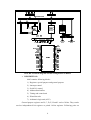
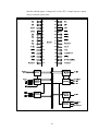
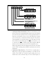
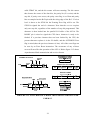
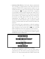
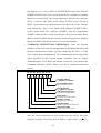
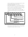
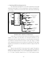
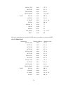
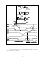
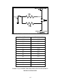
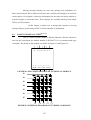
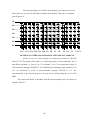
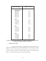
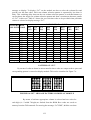
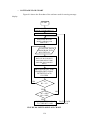
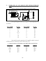
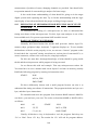
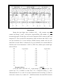
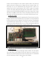
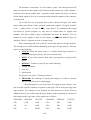
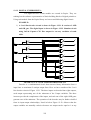
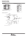
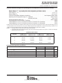
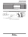
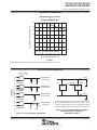
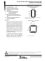
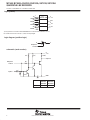
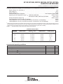
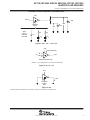
1
Saurashtra University Re – Accredited Grade ‘B’ by NAAC (CGPA 2.93) Nanavati, Maulin C., 2007, “The development of Advance Experiments useful to the students of Electronics field”, thesis PhD, Saurashtra University http://etheses.saurashtrauniversity.edu/id/912 Copyright and moral rights for this thesis are retained by the author A copy can be downloaded for personal non-commercial research or study, without prior permission or charge. This thesis cannot be reproduced or quoted extensively from without first obtaining permission in writing from the Author. The content must not be changed in any way or sold commercially in any format or medium without the formal permission of the Author When referring to this work, full bibliographic details including the author, title, awarding institution and date of the thesis must be given. Saurashtra University Theses Service http://etheses.saurashtrauniversity.edu [email protected] © The Author THE DEVELOPMENT OF ADVANCE EXPERIMENTS USEFUL TO THE STUDENTS OF ELECTRONICS FIELD Thesis Submitted to the Saurashtra University, Rajkot For The Degree of Doctor of Philosophy (Science) (Electronics) By Maulin Chandrakant Nanavati Department Of Electronics Saurashtra University Rajkot 360 005 Gujarat, India Research Supervisor Dr. H. N. Pandya Head Department Of Electronics Saurashtra University Rajkot 360 005 Gujarat, India MAY 2007 Erudition can only be got in one way, the way of experience; there is no other way. - Shri Swami vivakand Affectionately fanatical To My Adored Grandparents Mr. J. N. Nanavati and Mrs. H. J. Nanavati And My Parents Dr. C. J. Nanavati and Dr. B. C. Nanavati Statement under O. Ph.D. of Saurashtra University The content of this thesis is my own work carried out under the supervision of Dr. H. N. Pandya and leads to some contribution in Electronics supported by necessary references. (Mr. M. C. Nanavati) Department Of Electronics Saurashtra University, Rajkot 360 005 Gujarat, India This is to certify that the present work submitted by Mr. M. C. Nanavati for the Ph.D. degree of Saurashtra University, Rajkot has been the result of about 5 years of work under my supervision and is a valuable contribution in the field of electronics. Dr. H. N. Pandya Head, Department Of Electronics Saurashtra University, Rajkot 360 005 Gujarat, India. Acknowledgement I am thankful to my GOD LORD SHIVA for give me opportunity to gain a higher level education. I am thankful to Saurashtra University for register me as a research student and permit me to use laboratory and other available resources of Department and University. I am thankful to my GURU, Research advisor Dr. H. N. Pandya, Head Department Of Electronics, Saurashtra University, Rajkot, Gujarat, India for his keen interest in my research work and keep me morally boost in my difficulties and work-out to perform my research work easily. I am thankful to him for use his scientific and innovative idea for my research work. In deep sense of gratitude for my parent Dr. Basanti Chandrakant Nanavati and Dr. Chandrakant J. Nanavati, without there blessing and moral support I could not perform this task easily. I am especially thankful to my parents for there help in all regards and give me opportunity to gain a higher level education. Also I am thankful to Miss. Priti J. Joshi, Mr. J. B. Joshi, Mrs. S. J. Joshi, Mr. P. J. Joshi and Miss. B. J. Joshi for their moral support during my completion period of my Ph. D. work. I thankful to my colleagues Mr. Anand Bhaskar for plan out research problem and discuss on research problems. I am thankful to him for his helping hand on my research work. I am thankful to Dr. Kapil K. Bhatt lecturer, Department of Physics, Wilson College, Mumbai, Dr. Urmiben M. Joshi, and Dr. K. P. Thummer for their useful tips in research problems. I am thankful to my sister Mrs. Kruti Buch, my brother-in-law Mr. Harshal Buch for their love and help me in moral boost in my research work. I am thankful to my little nephew Mr. N. H. Buch whose smiling face makes my work easy and boost me for to cheer up me in my hard work. I am thankful to Mr. Udaybhai J. Khachar for his kind help during discussing on various problems. I am thankful to Mr. Jatin Kamdar, Dr. Bimal H. Vyas, Dr. Chetan M. Thakar, Mr. Jatin Joshi, Mr. Rajendrakumar Khar, Mr. Jaipalsinh Zala, and Mr. Hemanshu Vachhani for there moral support during my breakdowns and discussion on different topics. I am thankful to Mr. Manishbhai R. Pandya, Mr. Taresh P. Bhatt for their help to cheer up me in my tense and problematic days. I am thankful to Mr. Manishbhai for help me at Department of Electronics for providing me help at laboratory work. Last but not list I am thankful to Mrs. Kirenben H. Pandya (madam) and Miss S. H. Pandya for their help and moral boosting in tense matter. At the last I am again thankful to my GOD LORD SHIVA who gives me Power and strength to gain this higher degree of education and to fight against those problems to come over. I am thankful to Lord Shiva for his blessings. Thank you all of you, who help me during this period of education. - Maulin Chandrakant Nanavati Contents Title Quote Dedicated to Certificate Acknowledgement Section 1 AIMS AND TOOLS Chapter 1 Introduction. . . . . . . . . . . . . . . . . . . . . . . . . . . . . . . . . . . . . . . . . 1 Objective of the present work. . . . . . . . . . . . . . . . . . . . . 2 Literature survey. . . . . . . . . . . . . . . . . . . . . . . . . . . . . . . 2 Chapter 2 Basics of microprocessor 8085A. . . . . . . . . . . . . . . . . . . . . . . . Introduction. . . . . . . . . . . . . . . . . . . . . . . . . . . . . . . . . . Major blocks of microprocessor 8085. . . . . . . . . . . . . . General features. . . . . . . . . . . . . . . . . . . . . . . . . Description. . . . . . . . . . . . . . . . . . . . . . . . . . . . . Pin description. . . . . . . . . . . . . . . . . . . . . . . . . . Input / Output devices of microprocessor 8085. . . . . . . 82C55A Programmable Peripheral Interface. . . Functional description. . . . . . . . . . . . . . Operational description. . . . . . . . . . . . . Operating modes. . . . . . . . . . . . . . . . . . 8251A Universal Synchronous / Asynchronous Receiver and Transmitter. . . . . . Functional description. . . . . . . . . . . . . . . Operational description. . . . . . . . . . . . . . Programming the 8251A. . . . . . . . . . . . . Memory organization of 8085A. . . . . . . . . . . . . . . . . . . 6 7 7 7 8 10 13 13 13 17 20 Basics of microcontroller 89C51. . . . . . . . . . . . . . . . . . . . . . . . Introduction. . . . . . . . . . . . . . . . . . . . . . . . . . . . . . . . . . . Pin description. . . . . . . . . . . . . . . . . . . . . . . . . . . Major blocks of microcontroller 89C51. . . . . . . . . . . . . Special Function register. . . . . . . . . . . . . . . . . . . Input / Output devices of microcontroller 89C51. . . . . . P1- P3 structure and operation. . . . . . . . . . . . . . Reading the input pin. . . . . . . . . . . . . . . . . . . . . Writing “0” to the port. . . . . . . . . . . . . . . . . . . . Avoid damaging the port. . . . . . . . . . . . . . . . . . Instructions reading the status of input port. . . . Reading latch. . . . . . . . . . . . . . . . . . . . . . . . . . . . Read modify write instructions. . . . . . . . . . . . . . Output port. . . . . . . . . . . . . . . . . . . . . . . . . . . . . Memory organization of 89C51. . . . . . . . . . . . . . . . . . . Program memory. . . . . . . . . . . . . . . . . . . . . . . . 48 49 50 52 53 56 57 57 58 58 58 59 59 60 60 60 Chapter 3 29 29 35 36 44 Contents Data memory. . . . . . . . . . . . . . . . . . . . . . . . . . . Direct and Indirect address area. . . . . . . . . . . . . 60 61 Section 2 EXPERIMENTS ON MICROPROCESSOR Chapter 4 Advance experiments on 8251. . . . . . . . . . . . . . . . . . . . . . . . . . Roll of 8251 with microprocessor 8085. . . . . . . . . . . . . Continuous transmission of data over TXD pin. . . . . . . . 8251 as receiver and transmitter in the same kit. . . . . . . Serial communication between two kits. . . . . . . . . . . . . 62 63 71 73 75 Chapter 5 Advance experiments on 8255. . . . . . . . . . . . . . . . . . . . . . . . . . Roll of 8255 with microprocessor 8085. . . . . . . . . . . . . Mode 1 experiment. . . . . . . . . . . . . . . . . . . . . . . . . . . . . Port A as output port and port B as input Port in mode 1. . . . . . . . . . . . . . . . . . . . . . . . . . . Mode 2 experiment. . . . . . . . . . . . . . . . . . . . . . . . . . . . . Port A as output port and port B as input Port. . . . . . . . . . . . . . . . . . . . . . . . . . . . . . . . . . . Port A as input port and port B as output Port. . . . . . . . . . . . . . . . . . . . . . . . . . . . . . . . . . . 81 82 87 Chapter 6 Advance experiments on interrupt. . . . . . . . . . . . . . . . . . . . . . Roll of hardware and software interrupts with Microprocessor 8085. . . . . . . . . . . . . . . . . . . . . . . . . . . . To generate the interrupts as per user’s choice and execute its service routine. . . . . . . . . . . . . . . . . . . . . . . . To verify the priorities of interrupts. . . . . . . . . . . . . . . . To understand the masking of interrupts. . . . . . . . . . . . . 87 92 92 95 98 99 106 109 110 Section 3 EXPERIMENTS ON MICROCONTROLLER 89C51 Chapter 7 Advance experiments on Keyboard interface. . . . . . . . . . . . . Basics of keyboard used. . . . . . . . . . . . . . . . . . . . . . . . . Interfacing of keyboard with 89C51 Microcontroller. . . 111 112 113 Chapter 8 Advance experiments on matrix display. . . . . . . . . . . . . . . . . . Basics of display used. . . . . . . . . . . . . . . . . . . . . . . . . . . Basic knowledge of 5X7 matrix LED display. . . . . . . . Running character display interface using 89C51. . . . . . 126 127 128 128 Chapter 9 Advance experiments on LCD display. . . . . . . . . . . . . . . . . . . Introduction. . . . . . . . . . . . . . . . . . . . . . . . . . . . . . . . . . . Basics of LCD display. . . . . . . . . . . . . . . . . . . . . . . . . . . Interfacing of LCD module with microcontroller 89C51. . . . . . . . . . . . . . . . . . . . . . . . . . . . . . . . . . . . . . . 139 140 140 II 144 Contents Section 4 DEVELOPMENT TOOLS Chapter 10 Advance experiments on logic state analyzer. . . . . . . . . . . . . . Introduction. . . . . . . . . . . . . . . . . . . . . . . . . . . . . . . . . . . Debugging of microprocessor kit using logic state analyzer: a simple laboratory experiment. . . . . . . . . . . . 154 155 160 Chapter 11 Advance experiments on pcice. . . . . . . . . . . . . . . . . . . . . . . . . . 168 Introduction. . . . . . . . . . . . . . . . . . . . . . . . . . . . . . . . . . . 169 Using In-circuit emulator in the laboratory. . . . . . . . . . . 169 Chapter 12 Advance experiments on Pspice. . . . . . . . . . . . . . . . . . . . . . . . . Introduction. . . . . . . . . . . . . . . . . . . . . . . . . . . . . . . . . . . Commands of Pspice. . . . . . . . . . . . . . . . . . . . . . . . . . . . Experiments. . . . . . . . . . . . . . . . . . . . . . . . . . . . . . . . . . . Analog experiments. . . . . . . . . . . . . . . . . . . . . . . AC circuit. . . . . . . . . . . . . . . . . . . . . . . . DC circuit. . . . . . . . . . . . . . . . . . . . . . . . Digital experiments. . . . . . . . . . . . . . . . . . . . . . . 186 187 204 205 206 206 217 223 Chapter 13 Conclusion. . . . . . . . . . . . . . . . . . . . . . . . . . . . . . . . . . . . . . . . . . 241 Appendix A Datasheet. . . . . . . . . . . . . . . . . . . . . . . . . . . . . . . . . . . . . . . . . . . MC1488 Quadruple line drivers. . . . . . . . . . . . . . . . . . . . MC1489 Quadruple line receivers. . . . . . . . . . . . . . . . . . 243 Appendix B References. . . . . . . . . . . . . . . . . . . . . . . . . . . . . . . . . . . . . . . . . . 244 III Figures Figure 2.1…………………………………………………………………...8 Figure 2.2…………………………………………………………………...14 Figure 2.3…………………………………………………………………...16 Figure 2.4…………………………………………………………………...17 Figure 2.5…………………………………………………………………...18 Figure 2.6…………………………………………………………………...19 Figure 2.7…………………………………………………………………...21 Figure 2.8(A)……………………………………………………………......22 Figure 2.8(B)………………………………………………………………..22 Figure 2.9(A)………………………………………………………………..23 Figure 2.9(B)………………………………………………………………..24 Figure 2.10(A)………………………………………………………………26 Figure 2.10(B)………………………………………………………………26 Figure 2.11…………………………………………………………………..29 Figure 2.12…………………………………………………………………..30 Figure 2.13…………………………………………………………………..37 Figure 2.14…………………………………………………………………..38 Figure 2.15…………………………………………………………………..39 Figure 2.16…………………………………………………………………..40 Figure 2.17…………………………………………………………………..41 Figure 2.18…………………………………………………………………..42 Figure 2.19…………………………………………………………………..43 Figure 2.20…………………………………………………………………..44 Figure 2.21…………………………………………………………………..45 Figure 2.22…………………………………………………………………..46 Figure 2.23…………………………………………………………………..46 Figure 3.1..…………………………………………………………………..50 Figure 3.2..…………………………………………………………………..53 Figure 3.3..…………………………………………………………………..55 Figure 3.4..…………………………………………………………………..57 Figure 3.5..…………………………………………………………………..60 Figure 3.6..…………………………………………………………………..61 Figure 4.1..…………………………………………………………………..64 Figure 4.2..…………………………………………………………………..65 Figure 4.3..…………………………………………………………………..65 Figure 4.4..…………………………………………………………………..66 Figure 4.5..…………………………………………………………………..67 Figure 4.6..…………………………………………………………………..68 Figures Figure 4.7..…………………………………………………………………..69 Figure 4.8..…………………………………………………………………..70 Figure 4.9..…………………………………………………………………..70 Figure 4.10…………………………………………………………………..76 Figure 5.1(A).....…………………………………………………………......83 Figure 5.1(B).....…………………………………………………………......84 Figure 5.2..…………………………………………………………………..85 Figure 5.3..…………………………………………………………………..86 Figure 5.4..…………………………………………………………………..87 Figure 5.5(A).....…………………………………………………………......88 Figure 5.5(B).....…………………………………………………………......88 Figure 5.5(C).....…………………………………………………………......89 Figure 5.6..…………………………………………………………………..93 Figure 5.7..…………………………………………………………………..95 Figure 6.1..…………………………………………………………………..102 Figure 6.2..…………………………………………………………………..104 Figure 7.1..…………………………………………………………………..112 Figure 7.2..…………………………………………………………………..113 Figure 7.3..…………………………………………………………………..114 Figure 7.4..…………………………………………………………………..115 Figure 7.5..…………………………………………………………………..117 Figure 8.1..…………………………………………………………………..127 Figure 8.2..…………………………………………………………………..127 Figure 8.3..…………………………………………………………………..128 Figure 8.4..…………………………………………………………………..129 Figure 8.5..…………………………………………………………………..131 Figure 8.6..…………………………………………………………………..132 Figure 8.7..…………………………………………………………………..133 Figure 8.8..…………………………………………………………………..134 Figure 9.1..…………………………………………………………………..141 Figure 9.2..…………………………………………………………………..143 Figure 9.3..…………………………………………………………………..144 Figure 10.1…………………………………………………………………..156 Figure 10.2…………………………………………………………………..162 Figure 10.3…………………………………………………………………..163 Figure 10.4…………………………………………………………………..160 Figure 11.1…………………………………………………………………..181 Figure 12.1…………………………………………………………………..189 Figure 12.2…………………………………………………………………..190 Figure 12.3…………………………………………………………………..192 Figure 12.4…………………………………………………………………..193 Figure 12.5…………………………………………………………………..194 Figure 12.6…………………………………………………………………..199 Figure 12.7…………………………………………………………………..201 Figure 12.8…………………………………………………………………..206 Figure 12.9…………………………………………………………………..208 Figure 12.10..………………………………………………………………..209 Figure 12.11..………………………………………………………………..209 Figure 12.12..………………………………………………………………..210 Figure 12.13..………………………………………………………………..210 V Figures Figure 12.14..………………………………………………………………..216 Figure 12.15..………………………………………………………………..217 Figure 12.16..………………………………………………………………..218 Figure 12.17..………………………………………………………………..220 Figure 12.18..………………………………………………………………..221 Figure 12.19..………………………………………………………………..221 Figure 12.20..………………………………………………………………..222 Figure 12.21..………………………………………………………………..223 Figure 12.22..………………………………………………………………..224 Figure 12.23..………………………………………………………………..225 Figure 12.24..………………………………………………………………..230 Figure 12.25..………………………………………………………………..231 Figure 12.26(A).…………………………………………………………......232 Figure 12.26(B).…………………………………………………………......232 VI Tables Table 2.1…………………………………………………………………………… 16 Table 2.2…………………………………………………………………………… 20 Table 2.3…………………………………………………………………………… 27 Table 2.4…………………………………………………………………………… 47 Table 3.1…………………………………………………………………………… 52 Table 3.2…………………………………………………………………………… 54 Table 4.1…………………………………………………………………………… 73 Table 6.1……………………………………………………………………..…….100 Table 6.2……………………………………………………………………..…….100 Table 6.3……………………………………………………………………..…….103 Table 6.4………………………………………………………………………….. 104 Table 6.5………………………………………………………………………….. 105 Table 6.6………………………………………………………………………….. 105 Table 6.7………………………………………………………………………….. 106 Table 6.8………………………………………………………………………….. 109 Table 7.1(A)………………………………………………………………………. 115 Table 7.2(B)………………………………………………………………………. 116 Table 8.1………………………………………………………………………….. 130 Table 8.2………………………………………………………………………….. 131 Table 8.3………………………………………………………………………….. 132 Table 9.1………………………………………………………………………….. 139 Table 9.2………………………………………………………………………….. 140 Table 9.3………………………………………………………………………….. 142 Table 10.1………………………………………………………………………… 157 Table 10.2………………………………………………………………………… 167 Table 11.1………………………………………………………………………… 170 Table 11.2………………………………………………………………………… 172 Table 12.1………………………………………………………………………… 224 Table 12.2………………………………………………………………………… 231 VII SECTION 1 AIMS AND TOOLS CHAPTER 1 INTRODUCTION 1 1.1 Objective of the present work:In the last few years of this century the technology has spelled the society with miracles. The fast growth of electronics has opened a variety of advance topics to be learned by the students. The training to the newer topic in the electronics needs a structured easy to understand methodology. The in-flow of the newer and newer topics has surmounted the slow pace of learning. Students are desirous of learning many new things in electronics but the latest electronics topics have not been chewed by the faculties to feed the young ones, that is, students. It is our basic objective in the present work to convert such complex conceptual aspects to a level that can be easily understood by the student. We have developed the experiments which can train students to easily understand and verify the concepts themselves by performing experiment on there own. We also planed to prepare material regarding experiments which is included in the concerned experiments. Thus, the objectives of the present work is to design and develop experiments on advance topics like microprocessor, microcontroller, circuit simulation and on the development tool to help the students learn this topic with ease along with the study material. 1.2 Literature Survey:In the first attempt to gather information about the experiments in the field of electronics the books on such topic were searched. The well known books written by ZBAR PAUL B “Basic Electronics: A Text-Lab Manual”, 4th and 7th edition, Tata McGraw hill Publishing company Limited and listed below were studied. But, the content of the books were of basic electronics type. We tried to refer the various books on 8085 which may give some idea on the interfacing experiments on 8085. Some of the books we found useful are listed below[B-1 TO B-25]. 1) A. W. Moore, K. E. Fronheisher, Vinay Khanna, John DElaune, G. G. Sawyer, M. E. Edison, T. C. Daly, J. F. Vittera “Motorola semiconductor product Inc. Microprocessor1 applications manual” MCGraw hill publishing inc. N Y. 1 Motorola microprocessor 68C00 applications 2 2) Ahson S. L. “Microprocessor with application in process control” Tata MCGraw hill Publishing Company Limited New Delhi, 1992 3) Baker R. Jecob, Li Harry W, Boyce David E “CMOS Circuit design, layout and simulation”, Prentice hall of India. 4) Bose Sanjay “Digital System: From Gates to Microprocessor” 2nd edition, New Age International (P) ltd. 1992. 5) Dr. H. N. Pandya2 “Printed Circuit Board” Gujarat Granth Nirman Board Ahmedabad India. 6) Dr. H. N. Pandya “Understanding P.C.B. Designing software” 1st edition, Saurashtra University Rajkot 2006. 7) Electronics concepts handbook vol. 1 to 3 MCGraw hill publishing inc. N. Y., 8) Giacoletto “Electronics Designers’ handbook” 2nd edition, MCGraw hill publishing inc. 9) Hall Dougles “Microprocessor and Digital system” 2nd edition, Tata MCGraw hill Publishing Company Limited. 10) J. C. Whitaker “The Electronics Handbook” IEEE Press. 11) John Markus “Guidebook of Electronics Circuit”, MCGraw hill publishing inc.. 12) Kenneth J. Ayala “The 8051 microcontroller Architecture, Programming and Applications” 2nd edition, Penram International Mumbai. 13) Microprocessor Data handbook, Revised Edition, BPB Publication New Delhi 14) Osborne, Adam, “An Introduction to Microcomputers Volume 0 to 3” Adam Osborne and Associates, Inc. 1977. 15) P. K. Ghosh and P. R. Sridhar “0000 to 8085 Introduction to Microprocessor for Engineers and scientists” 2nd edition, Prentice hall of India EEE edition New Delhi. 16) Padmanbhan K. “Learn to use Microprocessor” 4th edition, EFY Enterprises (P) ltd. New Delhi, 1999. 17) R. S. Gaonkar “Microprocessor architecture, programming and application with the 8085” 3rd edition, Penram International Mumbai. 2 Head, Department Of Electronics, Saurashtra University, Rajkot, Gujarat, India 3 18) Rashid Mohammad “Spice for circuits and electronics using PSPICE” 2nd and 3rd edition, Prentice hall of India, Eastern Economy Edition New Delhi. 19) Singh Renu “Microprocessor Interfacing and Application” 2nd edition, New Age Publication (P) ltd., 2006. 20) Stan Gibilisco and Neil Sclater3 “Encyclopedia Of Electronics” 1st and 2nd edition, MCGraw hill publishing inc. N Y. 21) Taub Herbert “Digital circuits and microprocessor”, Tata MCGraw hill Publishing company Limited England, 1982. 22) Theagarajan R and Dhanasekaran S. “Microprocessor and its Applications” New Age international (P) ltd. New Delhi, 1997. 23) Titus Christopher A., Larsen David G., Titus Jonathan A. “8085A Cookbook” Howard W. Sams & Co., Inc. 1980. 24) Walter Bosshart “Printed Circuit Board: Design and Technology” Tata MCGraw hill Publishing company Limited New Delhi, 1993. Apart from the above books book on SDK-85 microprocessor trainer kit was found useful. The details of the book are as follow. 25) Borivaje Furht, Himansu Parikh “Microprocessor interfacing and communication using the Intel SDK-85” Prentice Hall, January 1986. We also used the internet facility to find out best useful in this work. This suggested us to following useful web-site[W-1 TO W-28]. • http://docs.hp.com/en/B6057-96002/ch04.html • http://groups.google.co.in/groups/dir?hl=en&sel=0,16823622, 16823610 • http://groups.google.co.in/sci.electronics.design?lnk=hppg&hl=en • http://linuxassembly.org/ • http://tech.groups.yahoo.com/group/emu8086/ • http://tech.groups.yahoo.com/group/win32-nasm-users/ • http://www.2cpu.com/ • http://www.8052.com/ • http://www.brothersoft.com/Home_Education_Science_8085_Simulatot _19818.html • 3 http://www.chip-architect.com/ Editor In-Chief MCGraw hill publishing inc. N.Y. 4 • http://www.clickon-cpu.com/ • http://www.cpu-museum.com/ • http://www.cpu-museum.net/ • http://www.datasheetcatalog.com/ • http://www.emu8086.com/ • http://www.emulation.com/ • http://www.emulators.com/pentium4.htm • http://www.freemware.org/ • http://www.ieee.org/ • http://www.intel.com/ • http://www.microprocessor.sscc.ru/ • http://www.old-computer.com/museum/computer.asp?st=1&c=805 • http://www.orcad.com • http://www.rdos.net/sim/ • http://www.thefreecountry.com/ • http://www.tomshardware.com/ • http://www.x86.org/ • http://www.x86-64.org/ The detailed literature survey suggested that we need to develop the study material on the concentrated topic like microprocessor, microcontroller, circuit simulation and development tools. 5 CHAPTER 2 BASICS OF MICROPROCESSOR 8085 6 2.1 INTRODUCTION:8085 is one of the topics of present work. Some experiments which can enlighten the basic concepts of 8085 was planned. To understand 8085 properly the concept like timing diagram, interrupts, and interfacing are necessary. For this, the basic block diagram, instruction set, and programming aspects are to be thoroughly understood. Following are necessary to study 8085. • Address, data and control bus. • Detailed knowledge of instruction sets • Timing process of 8085 • Basic programming technique. 2.2 MAJOR BLOCKS OF MICROPROCESSOR 8085:The block diagram of 8085A is shown in Figure 2.1. • GENERAL FEATURES:o It is a 40 pin DIP device o It is 8-bit parallel central processor o Needs +5V supply o Basic speed is 3 MHz and above o Has four vectored interrupts o Facility of serial Input-Output o Can handle decimal, binary and double precision arithmetic o Can access directly 64KB memory o On chip system controller and clock generator o 1.3 µs instruction cycle. FIGURE 2.1 Block diagram and Pin configuration of 8085A • DESCRIPTION:8085 contains following blocks: 1) Registers: special purpose and general purpose 2) Interrupt control 3) Serial I/O control 4) Address/data buffers 5) Timing and control unit 6) IR and decoder 7) Arithmetic logic unit (ALU) General purpose registers are B, C, D, E, H and L each of 8-bits. They can be used as independent 8-bit registers or paired 16-bits registers. Following pairs are 8 possible: BC, DE and HL. Pairs are used for 16-bit arithmetic and to address the data in memory. HL is as special type of pair which always stores the address of memory location for accessing. Special purpose registers are A, FLAGS, PC, SP and IR. The accumulator is one default operand storage register for some arithmetic and logical instruction, second operand can be register or memory. Flags register stores the result of arithmetic or logical instruction by setting or resetting the individual flip-flops. Following is the structure. CY = Carry flag, set when carry or borrow occurs P = Parity flag, set for even parity AC = Auxiliary flag, set when carry occur due to operation of D3 digit. Used for BCD arithmetic. Z = Zero flag, set if the result is zero. S = Sign flag, set if the result is negative number. Stack pointer register always points to the last byte of the stack (at TOS). Filling up of stack decrements SP while retrieving of stack increments SP. Used by PUSH and POP instruction. Instruction register is not user accessible. It stores the op-code byte of any instruction and gives this information to decoder (instruction decoder). Interrupt control unit takes care of following interrupts. INTR, RST 7.5, RST 6.5, RST 5.5 and TRAP. They are written (above) in their increasing priority. TRAP is non-maskable. Except TRAP other interrupts can be enabled or disabled by interrupt enable (EI) or DI instructions. RST means restart (execution from predefined location). They have vectored addresses. RST 6.5, RST 5.5 and INTR are level sensitive, while RST 7.5 is edge sensitive. TRAP is edge and level sensitive. Sampling of interrupts takes place one cycle before the last cycle of the instruction being executed on the descending edge of the clock pulse. 9 A valid interrupt must occur at least 160ns before sampling time. RSTs interrupts are masked by SIM instruction and can be read off by RIM instruction. Serial input/output is possible through SID and SOD pins of 8085. For each bit transaction, SIM or RIM instruction is to be executed. RIM inputs bits while SIM outputs the bits. 8085 has multiplexed address and data lines (AD7 – AD0) (LOW ADDRESS LINES). During T1 clock cycle, high ALE latches address present on AD0-AD7 pins into external latch. During other clock cycles (T2, T3 …) same pins i.e. AD0-AD7 work as data lines D7-D0. Timing and control unit includes pins for clock, control signal (RD, WR, READY and ALE), status lines (S0, S1 and IO/ M), DMA (HOLD, HLDA) and reset (RESETIN, RESETOUT). Clock is provided by crystal (>6 MHz frequency). Crystal frequency is internally divided by 2. READY is for synchronization of external slow memory or device, S0, S1 and IO/ M are for hardware debugging and represent machine status. HOLD and HLDA are used for DMA application. RESETIN is for 8085A initialization and RESETOUT for peripheral initialization. IR and decoder are for instruction code byte storage and identification of the type of instruction. ALU can perform arithmetic and logical operation on operands of 8-bit length. These two operands are stored in A and one temporary register before ALU operation. Some results of instruction execution are provided in flag register by ALU. • PIN DISCRIPTION: A8 – A15 (OUTPUT 3-STATE) PIN NO. 21 TO 28 Address bus; the most significant 8-bits of the memory address or the 8-bits of the I/O address, 3-state during Hold and Halt modes. AD0 – AD7 (INPUT OUTPUT 3-STATE) PIN NO. 12 TO 19 Multiplexed address / data bus: Lower 8-bits of the memory address (or I/O address) appear on the bus during the first clock cycle of the machine state. It then becomes the data bus during the second and third clock cycles. 3-state during HOLD and HALT modes. ALE (OUTPUT) PIN NO. 30 Address latch enable: It occurs during the first clock cycle of a machine state and enables the address to get latched into the on-chip latch of peripherals. 10 The falling edge of ALE is set to guarantee setup and hold times for the address information. ALE can also be used to strobe the status information. ALE is never 3-stated. S0, S1 (OUTPUT) PIN NO. 29 & 33 Data bus status: encoded status of the bus cycle. S0 S1 Cycle 0 0 HALT 0 1 WRITE 1 0 READ 1 1 FETCH S1 can be used on an advanced R/W status. RD (OUTPUT 3-STATED) PIN NO. 32 READ: indicates the selected memory or I/O device is to be read and that the data bus is available for the data transfer. 3-stated during HOLD and HALT. WR (OUTPUT 3-STATED) PIN NO. 31 WRITE: indicates the data on the data bus is to be written into the selected memory or I/O device. Data is set up at the trailing edge of WR. 3-state during HOLD and HALT modes. READY (INPUT) PIN NO. 35 If READY is high during a read or writes cycle it indicates that the memory or peripheral is ready to send or receive data. If READY is low, the CPU will wait for READY to go high before completing the read or write cycle. HOLD (INPUT) PIN NO. 39 HOLD: indicates that another master is requesting the use of the address and data buses. The CPU, upon receiving the hold request, will relinquish the use of buses soon after the completion of the current machine cycle. Internal processing can regain the buses only after the HOLD is removed. When the HOLD is acknowledged, the Address, Data, RD, WR, and IO/M lines are 3stated. HLDA (OUTPUT) PIN NO. 38 HOLD ACKNOWLEDGE: indicates that the CPU has received the HOLD request and that it will relinquish the buses in the next clock cycle. HLDA 11 goes low after the HOLD request is removed. The CPU takes the buses one half clock cycles after HLDA goes low. INTR (INPUT) PIN NO. 10 INTERRUPT REQUEST: is used as a general purpose interrupt. It is sampled only during the next to the last clock cycle of the instruction. If it is active, the program counter (PC) will be inhibited from incrementing and an INTA will be issued. During this cycle a RESTART or CALL instruction can be inserted to jump to the interrupt service routine. The INTR is enabled and disable by software. It is disabled by RESET and immediately after an interrupt is accepted. INTA (OUTPUT) PIN NO. 11 INTERRUPT ACKNOWLEDGE: is used instead of (and has the same timing as) RD during the instruction cycle after an INTR is accepted. It can be used to activate the 8259 INTERRUPT CHIP or some other INTERRUPT PORT. RST 5.5, RST 6.5 AND RST 7.5 (INPUTS) PIN NO. 9, 8 AND 7 RESTART INTERRUPTS: These three inputs have the same timing as INTR except they cause an internal RESTART to be automatically inserted. Priority is highest for RST 7.5 then RST 6.5 and lastly RST 5.5. All these have higher priority then INTR. TRAP (INPUT) PIN NO. 6 TRAP INTERRUPT: is a non-maskable restart interrupt. It is recognized at the same time as INTR. It is unaffected by any mask or INTERRUPT enable. It has the highest priority of any interrupt. RESETIN (INPUTS) PIN NO. 36 RESET sets the program counter to zero and resets the INTERRUPT Enable and HLDA flip-flop. None of the other flags or registers (except the Instruction Register) are affected. The CPU is held in the reset condition as long as reset is applied. RESETOUT (OUTPUTS) PIN NO. 3 Indicates CPU is being reset. It can be used as a system RESET. The signal is synchronized to the processor clock. 12 X1, X2 (INPUTS) PIN NO. 1 AND 2 Crystal or R-C network connections to set the internal clock generator. X1 can also be an external clock input instead of crystal. The input frequency is divided by 2 to give the internal operating frequency. CLKOUT (OUTPUTS) PIN NO. 37 Clock output for use as a system clock when a crystal or R-C network is used as an input to the CPU. The period of CLK is twice the X1, X2 input period. IO/M (OUTPUTS) PIN NO. 34 IO/M indicates whether the read/write is to memory or I/O device. 3-stated during HOLD and HALT mode. SID (INPUTS) PIN NO. 5 Serial data input line. The data on this line is loaded into accumulator bit 7 whenever a RIM instruction is executed. SOD (OUTPUTS) PIN NO. 4 Serial data output line. The output SOD is set or reset as specified by the SIM instruction. VCC: +5 V supply PIN NO. 40 VSS: Ground reference PIN NO. 20 2.3 INPUT/OUTPUT DEVICES OF MICROPROCESSOR 8085: 8085A processor can be interfaced with various I/O devices through their controller peripheral chips. We have considered in present work following peripheral chips. 1. 82C55A (PPI) :- Programmable Peripheral Interface. 2. 8251A (USART):- Universal Synchronous/Asynchronous Receiver and Transmitter. 2.3.1 82C55A Programmable Peripheral Interface (PPI)4:Figure 2.2 shows Pin diagram and block diagram of 82C55A PPI chip. • FUNCTIONAL DESCRIPTION:• Data Bus buffer: - This 3-state bi-directional 8-bit buffer is used to interface the 82C55A to the system data bus. Data is transmitted or received by the 4 82C55A Programmable Peripheral Interface (PPI) INTEL® Datasheet 13 buffer upon execution of input or output instructions by the CPU. Control words and status information are also transferred through the data bus buffer. FIGURE 2.2 Pin description and Functional block diagram of 82C55A 14 • Read/write and control logic: - The function of this is to manage all of the internal and external transfers of both Data and Control or status words. It accepts inputs from the CPU Address and Control buses and in turn, commands to both of the Control Groups. (CS) Chip Select. A “LOW” on this input pin enables the communication between the 82C55A and the CPU. (RD) Read. A “LOW” on this input pin enables the 82C55A to send the data or status information to the CPU on the data bus. In essence, it allows the CPU to “read from” the 82C55A. (WR) Write. A “LOW” on this input pin enables the CPU to write data or control words into the 82C55A. (A0 and A1) port select 0 and port select 1. These input signals, in conjunction with the RD and WR inputs, control the selection of one of the three ports or the control word register. They are normally connected to the least significant bits of the address bus (A0 and A1). (RESET) Reset. A “HIGH” on this input initializes the control register to 9BH and all ports (A, B, C) are set to the input mode. “Bus hold” devices internal to the 82C55A will hold the I/O port inputs to a logic “1” state with a maximum hold current of 400µA. • Group A and Group B controls: - The functional configuration of each port is programmed by the systems software. In essence, the CPU “outputs” a control word to the 82C55A. The control word contains information such as “mode”, “bit set”, bit reset”, etc., that initializes the functional configuration of a 82C55A. Each of the control blocks (Group A and Group B) accepts “commands” from the Read/Write Control logic, receives “control words” from the internal data bus and issues the proper commands to its associated ports. Control Group A – Port A and Port C upper (C7 – C4) Control Group B – Port B and Port C lower (C3 – C0) The control word register can be both written and read as shown in the “Basic Operation” table. Figure 2.3 shows the control word format for both read and write operations. When the control word is read, bit D7 will always be a logic “1”, as this implies control word mode information. 15 FIGURE 2.3 Mode definition format for 82C55A A1 A0 RD WR CS INPUT OPERATION (READ) 0 0 0 1 0 PORT A Data bus 0 1 0 1 0 PORT B Data bus 1 0 0 1 0 PORT C Data bus 1 1 0 1 0 Control word Data bus OUTPUT OPERATION (WRITE) 0 0 1 0 0 Data bus Port A 0 1 1 0 0 Data bus port B 1 0 1 0 0 Data bus port C 1 1 1 0 0 Data bus Control word DISABLE FUNCTION X X X X 1 Data bus Three-state X X 1 1 0 Data bus Three-state Table 2.1 82C55A BASIC OPERATION 16 • Ports A, B and C: - The 82C55A contains three 8-bit ports (A, B and C). All can be configured to a wide variety of functional characteristics by the system software but each has its own special features or “personality” to further enhance the power and flexibility of the 82C55A. FIGURE 2.4 BUS-HOLD CONFIGURATION Port A One 8-bit data output latch/buffer and one 8-bit data input latch. Both “pull-up” and “pull-down” bus-hold devices are present on port A. Bus-hold configuration for port A is shown in figure 2.4 (A). Port B One 8-bit data input/output latch/buffer and one 8-bit data input buffer. Bus-hold configuration for port B is shown in figure 2.4 (B). Port C One 8-bit data output latch/buffer and one 8-bit data input buffer (no latch for input). This port can be divided into two 4-bit ports under the mode control. Each 4-bit port contains a 4-bit latch and it can be used for the control signal output and status signal inputs in conjunction with ports A and B. Bus-hold configuration for port C is shown in figure 2.4 (B). • Operational description:• Mode selection:- There are three basic modes of operation that can be selected by the system software: Mode 0 – Basic Input/Output Mode 1 – Strobed Input/Output Mode 2 – Bi-directional Bus 17 FIGURE 2.5 BASIC MODE DEFINITIONS AND BUS INTERFACE When the reset input goes “high”, all ports will be set to the input mode with all 24 port lines held at a logic “one” level by internal bus hold devices. After the reset is removed, the 82C55A can remain in the input mode with no additional initialization required. This eliminates the need to pull-up or pulldown resistors in all-CMOS designs. The control word register will contain 9BH. During the execution of the system program, any of the other modes may be selected using a single output instruction. This allows a single 82C55A to service a variety of peripheral devices with a simple software maintenance routine. Any port programmed as an output port is initialized to all zeros when the control word is written. The modes for port A and port B can be separately defined, while port C is divided into two portions as required by the Port A and Port B definitions. All of the output registers, including the status flip-flops, will be reset whenever the mode is changed. Modes may be combined so that their functional definition can be “tailored” to almost any I/O structure. The mode definitions and possible mode combination mode combinations may seem confusing at first, but after a cursory review of the complete device 18 operation a simple, logical I/O approach will surface. The design of the 82C55A has taken into account things such as efficient PC board layout, control signal definitions Vs. PC layout and complete functional flexibility to support almost any peripheral device with no external logic. Such design represents the maximum use of the available pins. • Single Bit Set/Reset feature: - Any of the eight bits of port C can be set or reset using a single Output instruction. This feature reduce software requirement in control-based application. When Port C is being used as status/control for Port A or B, these bits can be set or reset by using the Bit Set/Reset operation just as if they were output ports. Figure 2.5 shows Bit Set/Reset format for port C. FIGURE 2.6 Bit Set/Rest Format • Interrupt Control Functions:- When 82C55A is programmed to operate in mode 1 or mode 2, control signals are provided that can be used as interrupt request inputs to the CPU. The interrupt request signals, generated from port C, can be inhibited or enabled by setting or resetting the associated INTE flip-flop, using the bit set/reset of port C. This function allows the programmer to enable or disable a CPU interrupt by a specific I/O device without affecting any other device in the interrupt structure. 19 • INTE Flip-Flop Definition:(BIT-SET) – INTE is Set – Interrupt Enable (BIT-RESET) – INTE is Reset – Interrupt Disable • Operating Modes:• Mode 0 (basic Input/Output). This functional configuration provides simple input and output operations for each of the three ports. No handshaking is required; data is simply written to or read from specific port. Mode 0 Basic Functional Definitions Two 8-bit ports and two 4-bit ports Any port can be input or output Outputs are latched Input are not latched 16 different Input/Output configurations possible A B Group A PORT C PORT A (UPPER) Output Output # Group B PORT C PORT B (LOWER) Output Output D4 0 D3 0 D1 0 D0 0 0 0 0 1 Output Output 1 Output Input 0 0 1 0 Output Output 2 Input Output 0 0 1 1 Output Output 3 Input 0 1 0 0 Output Input 4 Input Output Output 0 1 0 1 Output Input 5 Output Input 0 1 1 0 Output Input 6 Input Output 0 1 1 1 Output 7 0 0 0 Input 8 Input Output Input 1 Input Output Output 1 0 0 1 Input Output 9 Output Input 1 0 1 0 Input Output 10 Input Output 1 0 1 1 Input Output 11 Input 1 1 0 0 Input Input 12 Input Output Output 1 1 0 1 Input Input 13 Output Input 1 1 1 0 Input Input 14 Input Output 1 1 1 1 Input Input 15 Input Input 0 Table 2.2 Mode 0 port definition 16 combination for input/out configuration 20 Mode 0 Basic Input Mode 0 Basic Output FIGURE 2.7 Mode 0 Basic Input/Output timing diagram • Mode 1 – (Strobed Input/Output). This functional configuration provides a means for transferring I/O data to or from a specified port in conjunction with strobes or “handshaking” signals. In mode 1, port A and port B use the lines on port C to generate or accept these “handshaking” signals. Mode 1 Basic function Definitions: Two Groups (Group A and Group B) Each group contains one 8-bit port and one 4-bit control/data port The 8-bit data port can be either input or output. Both inputs and outputs are latched The 4-bit is used for control and status of the 8-bit port. Input control Signal Definition: STB (Strobe Input). A “LOW” on this input loads data into the input latch. 21 FIGURE 2.8 (A) Mode 1 Strobed Input definitions FIGURE 2.8 (B) Mode 1 Strobed Input definitions timing diagram FIGURE 2.8 Input Control Signal definition IBF (Input Buffer Full flip-flop). A “HIGH” on this output indicates that the data has been loaded into the input latch: in essence, and 22 acknowledgment. IBF is set by STB input being low and reset by the rising edge of the RD input. INTR (Interrupt Request). A “HIGH” on this output can be used to interrupt the CPU when and input device is requesting service. INTR is set by the condition: STB is a “ONE”, IBF is a “ONE” and INTE is a “ONE”. It is reset by the falling edge of RD. This procedure allows an input device to request service from the CPU by simply strobing its data into the port. INTE A. Controlled by bit set/reset of PC4. INTE B. Controlled by bit set/reset of PC2. Output control Signal Definition: FIGURE 2.9 (A) Mode 1 Strobed Output definitions 23 FIGURE 2.9 (B) Mode 1 Strobed Output definitions timing diagram FIGURE 2.9 Output Control Signal definition OBF (Output Buffer Full Flip-flop). The OBF output will go “LOW” to indicate that the CPU has written data out to be specified port. This does not mean valid data is sent out of the port at this time since OBF can go true before data is available. Data is guaranteed valid at the rising edge of OBF. The OBF flip-flop will be set by the rising edge of the WR input and reset by ACK input being low. ACK (Acknowledge Input). A “LOW” on this input informs the 82C55A that the data from port A or port B is ready to be accepted. In essence, a response from the peripheral device indicating that it is ready to accept data. INTR (Interrupt Request). A “HIGH” on this output can be used to interrupt the CPU when an output device has accepted data transmitted by the CPU. INTR is set when ACK is a “ONE”, OBF is a “ONE” and INTE is a “ONE”. It is reset by the falling edge of WR. • Mode 2 - (Strobed Bi-Directional Bus I/O). The functional configuration provides a means for communicating with a peripheral device or structure on a single 8-bit bus for both transmitting and receiving data (BiDirectional bus I/O). “HANDSHAKING” signals are provided to maintain proper bus flow discipline similar to mode 1. Interrupt generation and enable/disable function are also available. Mode 2 Basic functional definitions: Used in Group A only One 8-bit, Bi-Directional bus port (port A) and 5-Bit control port (port C) 24 Both input and output are latched The 5-bit control port (port C) is used for control and status for the 8-bit, Bi-Directional bus port (port A) Bi-Directional Bus I/O Control Signal Definition: Mode 2 control word and Mode 2 configuration Mode 2 Bi-Directional timing diagram 25 FIGURE 2.10 (A) Mode 2 And Mode 0 Input/Output Configuration INTR (Interrupt Request). A high on this output can be used to interrupt the CPU for both input or output operations. FIGURE 2.10 (B) Mode 2 And Mode 1 Input/Output Configuration FIGURE 2.10 MODE 2 COMBINATIONS 26 Output operations OBF (Output Buffer Full). The OBF output will go “LOW” to indicate that the CPU has written data out to port A. ACK (Acknowledge). A “LOW” on this input enables the three-state output buffer of port A to send out the data. Otherwise, the output buffer will be in the high impedance state. INTE 1 (The INTE flip-flop associated with OBF). Controlled by bit set/reset of PC4. Input Operations STB (Strobe input). A “LOW” on this loads data into the input latch. IBF (Input Buffer Full Flip-Flop). A “HIGH” on this output indicates that data has been loaded into the input latch. INTE 2 (The INTE flip-flop associated with IBF). Controlled by bit set/reset of PC4. • Special mode combination considerations:- There are several combinations of modes possible. For any combination, some or all of port C lines are used for control or status. The remaining bits are either inputs or outputs as defined by a “Set Mode” command. During a read of port C, the state of all the port C lines, except the ACK and STB lines, will be placed on the data bus. In place of the ACK and STB line states, flag status will appear on the data bus in the PC2, PC4 and PC6 bit positions as illustrated by Table 2.3. INTERRUPT ALTERNATE PORT C ENABLE FLAG POSITION INTE B PC2 INTE A2 PC4 INTE A1 PC6 PIN SIGNAL (MODE) ACKB (Output Mode 1) or STBB (Input Mode 1) STBA (Input Mode 1 Or Mode 2) ACKA (Output Mode 1 Or Mode 2) TABLE 2.3 INTERRUPT ENABLE FLAGS IN MODE 1 AND MODE 2 Though a “Write port C” command, only the port c pins programmed as outputs in a Mode 0 group can be written. No other pins can be affected by a “Write port C” command, nor can the interrupt enable flags be accessed. 27 To write to any port C output programmed as an output in Mode 1 group or to change an interrupt enable flag, the “Set/Reset port C Bit” command must be used. With a “Set/Reset port C Bit” command, any port C line programmed as an output (including IBF and OBF) can be written or an interrupt enable flag can be either set or reset. Port C lines programmed as inputs, including ACK and STB lines, associated with Port C are not affected by a “Set/Reset port C Bit” command. Writing to the corresponding port C bit positions of the ACK and STB lines with the “Set/Reset port C Bit” command will affect the Group A and Group B interrupt enable flags, as shown in Table 2.3. • Current drive capability:- Any output on port A, B and C can sink or source 2.5mA. This feature allows the 82C55A to directly drive Darlington type drivers and high-voltage displays that require such sink or source current. • Reading Port C Status:- In Mode 0, Port C transfers data to or from the peripheral device. When the 82C55A is programmed to function in Modes 1 and 2, port C generates or accepts “handshaking” signals with the peripheral device. Reading the contents of signals of port C allows the programmer to test or verify the “status” of each peripheral device and change the program flow accordingly. There is not special instruction to read the status information form port C. A normal read operation of port C is executed to perform the function. 28 FIGURE 2.11 MODE 2 STATUS WORD FORMAT 2.3.2 8251A Universal Synchronous/Asynchronous Receiver and Transmitter (USART)5:Figure 2.12 shows Pin diagram and block diagram of 8251A PPI chip. • FUNCTIONAL DESCRIPTION:• General: - The 8251A is Universal Synchronous/Asynchronous Receiver/Transmitter designed for a wide range of Intel Microprocessor such like 8048, 8080, 8085, 8086 and 8088. Like other I/O devices in a microcomputer system, its functional configuration is programmed by the system’s software for maximum flexibility. The 8251A can support most serial data techniques in use, including IBM “Bi-sync”. In a communication environment an interface device must convert parallel format system data into serial format for transmission and convert incoming serial format data into parallel system data for reception. The interface device must also delete or insert bits or characters that are functionally unique to the communication technique. In essence, the 5 8251A Universal Synchronous/Asynchronous Receiver and Trasmitter (USART) INTEL® DATASHEET 29 interface should appear “transparent” to the CPU, a simple input or output of byte-oriented system data. FIGURE 2.12 PIN DISCRIPTION AND BLOCK DIAGRAM OF 8251A 30 • Data Bus Buffer: - This 3-state Bi-Directional, 8-bit buffer is use to interface the 8251A to the system Data Bus. Data is transmitted or received by the buffer upon execution of INput or OUTput instruction of the CPU. Control words, Command words and Status information are also transmitted through the Data Bus Buffer. The Command Status, 8-bit registers communicate with the system bus through the Data Bus Buffer. This functional block accepts inputs from the system Control bus and generates control signals for overall device operation. It contains the Control Word Register and Command Word Register that store the various control formats for the device functional definition. • RESET (Reset):- A “HIGH” on this input forces the 8251A into an “Idle” mode. The device will remain at “Idle” until a new set of control words is written into the 8251A to program its functional definition. Minimum RESET pulse width is 6 tCY (clock must be running). A command reset operation also puts the device into the “Idle” state. • CLK (Clock):- The CLK input is used to generate internal device timing and is normally connected to the Phase 2 (TTL) output of the Clock Generator. No external inputs or outputs are reference to CLK but the frequency of CLK must be greater then 30 times the Receiver or Transmitter data bit rate. • WR (Write):- A “LOW” on this input informs the 8251A that the CPU is writing data or control words to the 8251A. • RD (Read):- A “LOW” on this input informs the 8251A that the CPU is reading data or status information from the 8251A. • C/ D (control/Data):- This input, in conjunction with the WR and RD inputs, informs the 8251A that the word on the Data Bus is either a data character, control word or status information. 1 = control / status; 0 = data C/ D RD WR CS 0 0 1 0 8251A DATA DATA BUS 0 1 0 0 DATA BUS 8251A DATA 1 0 1 0 STATUS DATA BUS 1 1 0 0 DATA BUS CONTROL 31 X 1 1 0 DATA BUS 3-STATE X X X 1 DATA BUS 3-STATE • CS (Chip Select):- A “LOW” on this input selects the 8251A. No reading or writing will occur unless the device is selected. When CS is high, the Data Bus is in the float state and RD and WR have no effect on the chip. • Modem Control:- The 8251A has a set of control inputs and outputs that can be used to simplify the interface to almost any modem. The modem control signals are general purpose in nature and can be used for functions other then modem control, if necessary. • DSR (Data Set Ready):- The DSR output signal is a general-purpose, 1bit inverting output port. Its condition can be tested by the CPU using Status Read operation. The DSR input is normally used to test modem condition such as Data Set Ready. • DTR (Data Terminal Ready):- The DTR output signal is a generalpurpose, 1-bit inverting output port. It can be set “LOW” by programming the appropriate bit in the Command instruction word. The DTR output signal is normally used for modem control such Data Terminal Ready. • RTS (Request to Send):- The RTS output is signal is a general-purpose, 1-bit inverting output port. It can be set “LOW” by programming the appropriate bit in the Command instruction word. The RTS output signal is normally used for modem control such as Request to Send. • CTS (Clear to Send):- A “LOW” on this input enables the 8251A to transmit serial data if the TX Enable bit in the Command byte is set to a “ONE”. If either a TX Enable off or CTS off condition occures while, the TX will transmit all the data in the USART, written prior to TX Disable Command before shutting down. • Transmitter Buffer:- The transmitter Buffer accepts parallel data from the Data Bus Buffer, converts it to a serial bit stream, inserts the appropriate characters or bits (based on the communication technique) and output a composite serial stream of data on the TXD output pin on the falling edge TXC. The transmitter will begin transmission upon being enabled if CTS = 0. The TXD line will be held in the marking state 32 immediately upon a master Reset or when TX enable or CTS is off or the transmitter is empty. • Transmitter Control:- The transmitter Control manages all activities associated with the transmission of serial data. It accepts and issues signals both externally and internally to accomplish this function. • TXRDY (Transmitter Ready):- This output signals the CPU that the transmitter is ready to accept a data character. The TXRDY output pin can be used as an interrupt to the system, since it is masked by TXEnable; or for polled operatin, the CPU can check TXRDY using Status Read operation. TXRDY is automatically reset by the leading edge of WR when a data character is loaded from the CPU. Note that when using the polled operation, the TXRDY status bit is not masked by TXEnable, but will only indicate the Empty/Full Status of the TX Data Input Register. • TXE (Transmitter Empty):- When the 8251A has no characters to send, the TXEMPTY output will go “HIGH”. It resets upon receiving a character from CPU if the transmitter is enable. TXEMPTY remains high when the transmitter is disable. TXEMPTY can be used to indicate the end of a transmission mode, so that the CPU “knows” when to “turn the line around” in the half-duplex operational mode. In the Synchronous mode, a “HIGH” on this output indicates that a character has not been loaded and the SYNC character or characters are about to be or are being transmitted automatically as “fillers”. TXEMPTY does not go low when the SYNC characters are being shifted out. • TXC (Transmitter Clock):- The transmitter Clock controls the rate at which the character is to be transmitted. In the Synchronous transmission mode, the Baud Rate (1x) is equal to the TXC frequency. In Asynchronous transmission mode, the baud rate is a fraction of the actual TXC frequency. A portion of the mode instruction selects the factor: it can be 1, 1/16 or 1/64 the TXC. The falling edge of TXC shifts the serial data out of the 8251A. • Receiver Buffer:- The receiver accepts serial data, converts this serial input to parallel format, checks for bits or characters that are unique to the 33 communication technique and sends an “assembled” character to the CPU. Serial data is input to RXD pin, and is clocked in on the rising edge of RXC. • Receiver control:- This function block manage all receiver-related activity which consists of the following features. The RXD initialization circuit prevents the 8251A from mistaking an unused input line for an active low data line in the “break condition”. Before starting to receive serial characters on the RXD line, a valid “1” must first be detected after chip master Reset. Once this has been determined, a search for a valid low (Start bit) is enabled. This feature is only active in the asynchronous mode, and is only done once for each master Reset. The Flase Start bit detection circuit prevents false starts due to a transient noise spike by first detecting the falling edge and then strobing the normal center of the Start bit (RXD = low). Parity error detection sets the corresponding status bit. The framing Error status bit is set if the Stop bit is absent at the end of the data byte (asynchronous mode). • RXRDY (Receiver Ready):- This output indicates that the 8251A contains a character that is ready to be input to the CPU. RXRDY can be connected to the interrupt structure of the CPU or, for polled operation, the CPU can check the condition of RXRDY using a Status Read operation. RXEnable, when off, holds RXRDY in the Reset Condition. For Asynchronous mode, to set RXRDY, the Receiver must be enabled to sense a Start bit and a complete charater must be assembled and transferred to the Data Output Register. For Synchronous mode, to set RXRDY, the Receiver must be enabled and a character must finish assembly and be transferred to the Data Output Register. Failure to read the receiver character from the RX Data Output Register prior to the assembly of the next RX Data character will set overrun condition error and the previous character will be written over and lost. If the RX Data is being read by the CPU when the internal transfer is occurring, overrun error will be set and the old character will be lost. 34 • RXC (Receiver Clock):- The receiver Clock controls the rate at which the character is to be received. In the Synchronous mode, the Baud Rate (1x) is equal to the actual frequency of the RXC. In Asynchronous mode, the Baud Rate is a fraction of the actual RXC frequency. A portion of the mode instruction selects this factor: 1, 1/16 or 1/64 the RXC. Data is sampled into the 8251A on the rising edge of RXC. • SYNDET / BRKDET (SYNC Detect / Break Detect):- This pin is used in Synchronous mode for SYNDET and may be used as either input or output programmable through the Control Word. It is reset to output mode low upon RESET. When used as an output (internal Sync mode), the SYNDET pin will go “HIGH” to indicate that the 8251A has located the SYNC character in the Receive mode. If the 8251A is programmed to use double Sync characters (bi-sync), then SYNDET will go “HIGH” in the middle of the last bit of the second Sync character. SYNDET is automatically reset upon a Status Read operation. When used as an input (external SYNC detect mode), a positive going signal will cause the 8251A to start assembling data characters on the rising edge of the next RXC. Once in SYNC, the “HIGH” input signal can be removed. When External SYNC Detect is programmed, internal SYNC Detect is disabled. • BREAK (Async Mode Only):- This output will go high whenever the receiver remains low through two consecutive stop bit sequences (including the start bits, data bits, and parity bits). Break Detect may also be read as a Status bit. It is reset only upon master chip Reset or RX Data returning to a “one” state. • Operational description:• General:- The complete functional definition of the 8251A is programmed by the system’s software. A set of control words must be sent out by the CPU to initialize the 8251A to support the desired communications format. These control words will program the: BAUD RATE, CHARACTER LENGTH, NUMBER OF STOP BITS, SYNCHRONOUS or a SYNCHRONOUS OPERATION, EVEN/ODD/OFF PARTY, etc. in the 35 synchronous mode, operations are also provided to select either internal or external synchronization. Once programmed, the 8251A is ready to perform its communication functions. The TXRDY output is raised “HIGH” to signal the CPU that the 8251A is ready to receive a data character from the CPU. This output (TXRDY) is reset automatically when the CPU writes a character into the 8251A. On the other hand, the 8251A receives serial data from the MODEM or I/O device. Upon receiving an entire character, the RXRDY is raised “HIGH” to signal the CPU that the 8251A has a complete character ready for the CPU to fetch. RXRDY is reset automatically upon the CPU data read operation. The 8251A cannot begin transmission until the TXENABLE (Transmitter Enable) bit is set in the Command instruction and it has received a Clear To Send (CTS) input. The TXD output will be held in the marking state upon Reset. • Programming the 8251A:- Prior to starting data transmission or reception, the 8251A must be loaded with a set of control words generated by the CPU. These control signals define the complete functional definition of the 8251A and must immediately follow a Reset operation (internal or external) The control words are split into two formats: 1. Mode instruction 2. Command instruction Mode instruction:- This instruction defines the general operational characteristics of the 8251A. It must follow a Reset operation (internal or external). Once the Mode instruction has been written into the 8251A by the CPU, SYNC characters or Command instructions may be written. Command instruction:- This instruction defines a word is used to control the actual operation of the 8251A. Both the Mode and Command instructions must conform to a specified sequence for proper device operation. The Mode instruction must be written immediately following a Reset operation, prior to using the 8251A for data communication. 36 C/D = 1 MODE INSTRUCTION C/D = 1 SYNC CHARACTER 1 C/D = 1 SYNC CHARACTER 2 C/D = 1 COMMAND INSTRUCTION C/D = 0 DATA C/D = 1 COMMAND INSTRUCTION C/D = 0 DATA C/D = 1 COMMAND INSTRUCTION SYNC MODE ONLY FIGURE 2.13 TYPICAL DATA BLOCK All control words written into the 8251A after the Mode instruction will load the Command instruction. Command instructions can be written into the 8251A at any time in the data block during the operation of the 8251A. To return to the Mode instruction format, the master Reset bit in the Command instruction word can be set to initiate an internal Reset operation which automatically places the 8251A back into the Mode instruction format. Command instructions must follow the Mode instruction or Sync characters. • Mode Instruction Definition: - The 8251A can be used for either Asynchronous or Synchronous data communication. To understand how the Mode instruction defines the functional operation of the 8251A, the designer can best view the device as two separate components, one Asynchronous and other Synchronous, sharing the same package. The format definition can be changed only after a Master Chip Reset. For explanation purposes the two formats will be isolated. When parity is enabled it is not considered as one of the data bits for the purpose of programming word length. The actual parity bit received on the RX Data line cannot be read on the Data Bus. In the case of programmed character length of less then 8-bits, the least significant Data Bus bits will hold the data; unused bits are “don’t care” when writing data to the 8251A and will be “zeros” when reading the data from the 8251A. Below Figure 2.14 shows Mode instruction format for Asynchronous Mode. 37 FIGURE 2.14 ASYNCHRONOUS MODE INSTRUCTION FORMAT • Asynchronous Mode (Transmission):- Whenever a data character is sent by the CPU the 8251A automatically adds a Start bit (low level) followed by the data bits (least significant bit first), and the programmed number of Stop bits to each character. Also, an even or odd Parity bits is inserted prior to the Stop bit(s), as defined by the Mode instruction. The character is then transmitted as a serial data stream on the TXD output. The serial data is shifted out on the falling edge of the TXC at a rate equal to 1, 1/16 or 1/64 that of the TXC, as defined by the Mode instruction. BREAK characters can be continuously sent to the TXD if commanded to do so. When no data characters have been loaded into the 8251A the TXD output remains “HIGH” (marking) unless a BREAK (continuously low) has been programmed. • Asynchronous Mode (Receiver):- The RXD line is normally high. A falling edge on this line triggers the beginning of a START bit. The validity of this START bit is checked by again strobing this bit at its nominal center (16X or 64X mode only). If a low is detected again, it is 38 valid STRAT bit, and the bit counter will start counting. The bit counter thus locates the center of the data bits, the parity bit (if it exists) and the stop bit, if parity error occurs, the parity error flag is set. Data and parity bits are sampled on the RXD pin with the rising edge of the RXC. If a low level is detect as the STOP bit the Framing Error flag will be set. The STOP bit signals the end of a character. Note that the receiver requires only one stop bit, regardless of the number of stop bit programmed. This character is then loaded into the parallel I/O buffer of the 8251A. The RXRDY pin is raised to signal the CPU that a character is ready to be fetched. If a previous character has not been fetched by the CPU, the present character replaces it in the I/O buffer, and the OVERRUN Error flag is raised (thus the previous character is lost). All of the error flags can be reset by an Error Reset instruction. The occurrence of any of these errors will not affect the operation of the 8251A. Below figure 2.15 shows Asynchronous Mode transmission and receiver format. FIRGURE 2.15 ASYNCHRONOUS MODE TRANSMITER AND RECEIVER FORMAT 39 • Synchronous Mode (Transmission):- The TXD output is continuously high until the CPU sends its first character to the 8251A which usually is a SYNC character. When the CTS line goes low, the first character is serially transmitted out. All characters are shifted out on the falling edge of TXC. Data is shifted out at the same rate as the TXC. Once transmission has started, the data stream at the TXD output must continue at the TXC rate. If the CPU does not provide the 8251A with a data character before the 8251A Transmitter Buffers become empty. The SYNC characters (or character if in single SYNC character mode) will be automatically inserted in the TXD data stream. In this case, the TXEMPTY pin is raised high to signal that the 8251A is empty and SYNC characters are bing sent out. TXEMPTY does not go low when SYNC is being shifted out. The TXEMPTY pin is internally reset by a data character being written into the 8251A. Below Figure 2.16 shows Mode instruction format for Synchronous Mode. FIGURE 2.16 SYNCHRONOUS MODE INSTRUCTION FORMAT 40 • Synchronous Mode (Receive):- In this mode, character synchronization can be internally or externally achieved. If the SYNC mode has been programmed, ENTER HUNT command should be included in the first command instruction word written. Data on the RXD pin is then sampled on the rising edge of RXC. The content of the RX buffer is compared at every bit boundary with the first SYNC character until a match occurs. If the 8251A has been programmed for two SYNC characters, the subsequent received character is also compared; when both SYNC characters have been detected, the USART ends the HUNT mode and is in character synchronization. The SYNDET pin is then set high, and is reset automatically by the STATUS READ. If parity is programmed, SYNDET will not be set until the middle of the parity bit instead of the middle of the last data bit. In the external SYNC mode, synchronization is achieved by applying a high level on the SYNDET pin, thus forcing the 8251A out of the HUNT mode. The high level can be removed after one RXC cycle. An ENTER HUNT command has no effect in the Asynchronous mode of operation. Parity error and overrun error are both checked in the same way as in the Asynchronous RX mode. Parity is checked when not in HUNT, regardless of whether the receiver is enabled or not. FIGURE 2.17 SYNCHRONOUS MODE DATA FORMAT The CPU can command the receiver to enter the HUNT mode if synchronization is lost. This will also set all the used character bits in the buffer to a “one”, thus preventing possible false SYNDET caused by data 41 that happens to be in RX Buffer at ENTER HUNT time. Note that the SYNDET FLIP-FLOP is reset at each Status Read, regardless of whether internal or external SYNC has been programmed. This does not cause the 8251A to return to the HUNT mode. When in SYNC mode, but not in HUNT, Sync detection is still functional, but only occurs at the “known” word boundaries. Thus, if one Status Read indicates SYNDET and a second Status Read also indicates SYNDET, then the programmed SYNDET characters have been received since the previous Status Read. When external SYNDET mode is selected, internal Sync detect is disabled, and the SYNDET FLIP-FLOP may be set at any bit boundary. • COMMAND INSTRUCTION DEFINITION:- Once the function definition of the 8251A has been programmed by the Mode instruction and the Sync characters are loaded (if in Sync mode) then the device is ready to be used for data communication. The Command instruction controls the actual operation of the selected format. Functions such as: Enable Transmit/Receive, Error Reset and Modem Controls are provided by the Command instruction. Below Figure 2.18 shows command instruction format. D7 D6 D5 D4 D3 D2 D1 D0 EH IR RTS ER SBRK RxE DTR TxEN TRANSMIT ENABLE 1 = ENABLE, 0 = DISABLE DATA TERMINAL READY High will force DTR output to zero RECEIVE ENABLE 1 = ENABLE, 0 = DISABLE SEND BREAK CHARACTER 1 forces TxD low, 0 Normal operation ERROR RESET 1 resets error flags, 0 Normal operation REQUEST TO SEND High will force RST output to zero INTERNAL RESET High returns 8251 to Mode Instruction Format ENTER HUNT MODE 1 enables search for Sync characters FIGURE 2.18 COMMAND INSTRUCTION FORMAT Once the mode instruction has been written into the 8251A and Sync character inserted of necessary, then all further “control writes” (C/ D = 1) 42 will load a command instruction. A Reset Operation (internal or external) will return the 8251A to the Mode Instruction format. • STATUS READ DEFINITION:- In data communication systems it is often necessary to examine the “status” of the active device to ascertain of errors have occurred or other conditions that require the processor’s attention. The 8251A has facilities that allow the programmer to “read” the status of the device at any time during the functional operation. A normal “read” command is issued by the CPU with C/ D = 1 to accomplish this function. Below Figure 2.19 shows Status read format for 8251A. FIGURE 2.19 STATUS READ FORMAT Some of the bits in the Status Read format have identical meaning to external output pins so that the 8251A can be used in a completely polled or interrupt-driven environment. TXRDY is an exception. 43 2.4 MEMORY ORGANIZATION OF 8085A6,7,8,:8085A is mostly interfaced with RAM and EPROM memory chips. We know that 8085A has 16-address lines. This enables it to address 64 Kilobytes (KB) of memory locations. To make a useful system 8085 generally EPROM and RAM chips together comprise this address space. 6264 is a commonly used RAM chip with 2764A and 27128 EPROM chips widely used chip with 8085A. Figure 2.20 and 2.21 shows pin diagram of EPROM 2764A and RAM 6264 respectively. The address space of 8085A in Hexadecimal (HEX) location induces from 0000H to FFFFH. Normally, in memory organization of 8085A first few Kilobytes of memory locations are used for EPROM area and rest are used for RAM area. A typical memory organization of 8085A is shown in Figure 2.22 and 2.23. For interfacing 2764A with 8085A a decoder 74LS155 and a latching IC 74LS373 are used. The interfacing circuit for the same is shown in Figure 2.23. Note that this circuit is a part of the detailed circuitry of microprocessor trainer kit. FIGURE 2.20 PIN DIAGRAM OF 2764A EPROM 6 “0000 to 8085 Introduction to Microprocessor for Engineers and scientists” 2nd edition, P. K. Ghosh and P. R. Sridhar 7 “Microprocessor Architecture, Programming and Application with the 8085” 3rd Ed, R. S. Gaonkar 8 Intel® Datasheet 44 FIGURE 2.21 PIN DIAGRAM OF 6264 RAM IC 74LS373 de-multiplexes the AD0 to AD7 lines of 8085A, when ALE becomes high and it enables IC 74LS373 trough its pin no. 11 (G), to latch the address A0 to A7. Active low enable pin no. 1 that is OC of IC 74LS373 is permanently grounded. The output of Q0 to Q7 of IC 74LS373 (i.e. A0 to A7 address lines) are connected with the address lines A0 to A7 of EPROM 2764A. The rest of the address lines of 2764A, i.e. A8 to A12 address lines are connected with corresponding address lines of 8085A. The EPROM 2764A has a pin named OE which helps to read data out. This OE pin directly connected with the RD of 8085A. Also pin PGM and VPP are connected with VCC. 45 U1 36 1 2 5 6 9 8 7 10 11 29 33 39 35 U2 RST-IN X1 X2 SID TRAP RST 5.5 RST 6.5 RST 7.5 INTR AD0 AD1 AD2 AD3 AD4 AD5 AD6 AD7 A8 A9 A10 A11 A12 A13 A14 A15 INTA S0 S1 HOLD READY ALE WR RD IO/M RST-OT CLKO SOD HLDA 12 13 14 15 16 17 18 19 21 22 23 24 25 26 27 28 3 4 7 8 13 14 17 18 1 11 D0 D1 D2 D3 D4 D5 D6 D7 U4 2 5 6 9 12 15 16 19 Q0 Q1 Q2 Q3 Q4 Q5 Q6 Q7 10 9 8 7 6 5 4 3 25 24 21 23 2 OC G 74LS373 20 22 27 1 30 31 32 34 3 37 4 38 A0 A1 A2 A3 A4 A5 A6 A7 A8 A9 A10 A11 A12 11 12 13 15 16 17 18 19 O0 O1 O2 O3 O4 O5 O6 O7 CE OE PGM VPP 2764 VCC 8085 U3 13 3 2 1 14 15 A B 1G 1C 2G 2C 7 6 5 4 9 10 11 12 1Y0 1Y1 1Y2 1Y3 2Y0 2Y1 2Y2 2Y3 74LS155 Figure 2.22 EPROM 2764 INTERFACING CIRCUIT FOR 8085A U1 36 1 2 5 6 9 8 7 10 11 29 33 39 35 RST-IN X1 X2 SID TRAP RST 5.5 RST 6.5 RST 7.5 INTR U2 AD0 AD1 AD2 AD3 AD4 AD5 AD6 AD7 A8 A9 A10 A11 A12 A13 A14 A15 INTA S0 S1 HOLD READY ALE WR RD IO/M RST-OT CLKO SOD HLDA 12 13 14 15 16 17 18 19 21 22 23 24 25 26 27 28 3 4 7 8 13 14 17 18 1 11 D0 D1 D2 D3 D4 D5 D6 D7 U4 Q0 Q1 Q2 Q3 Q4 Q5 Q6 Q7 2 5 6 9 12 15 16 19 10 9 8 7 6 5 4 3 25 24 21 23 2 OC G 74LS373 20 26 27 22 30 31 32 34 3 37 4 38 A0 A1 A2 A3 A4 A5 A6 A7 A8 A9 A10 A11 A12 D0 D1 D2 D3 D4 D5 D6 D7 11 12 13 15 16 17 18 19 CS1 CS2 WE OE MCM6264 VCC 8085 U3 13 3 2 1 14 15 A B 1G 1C 2G 2C 1Y0 1Y1 1Y2 1Y3 2Y0 2Y1 2Y2 2Y3 7 6 5 4 9 10 11 12 74LS155 Figure 2.23 RAM 6264 INTERFACING CIRCUIT FOR 8085A The chip selection is controlled by the decoder 74LS155. 74LS155 is used to select the memory chips 2764A (EPROM), 6264 (RAM) and I/O chips 8279 and 8255. 46 To separate the memory and I/O device the output pins of 74LS155 are divided into two groups that is 1Y0, 1Y1, 1Y2 and 1Y3 are for I/O device selection and 2Y0, 2Y1, 2Y2 and 2Y3 are for memory chip selection. 74LS155 has four enable pins out of which three are active low and one remaining two (where one is active low and another is active high) are connected with IO/ M pin of 8085A. Here, active high is connected with enabling of outputs of internal decoder 1 of 74LS155. While active low is connected with the internal decoder-2 of 74LS155. Hence, whenever IO/ M pin of 8085A is high, I/O devices are selected, and when IO/ M is low, memory chips are selected. This we can explain as below table 2.4 IO/ M A (A14) B (A15) 0 0 0 EPROM 2764A (2Y0) 0 1 0 RAM 6264 (2Y1) SELECTION TABLE 2.4: SELECTION USING ADDRESS LINES The interfacing circuit of RAM 6264 involves 74LS373 and 74LS155 and 8085. IC 74LS373 and 74LS155 are having the same connection details with the 8085A as discussed above. The only difference in this one is that the A and B input lines of 74LS155 selects 6264 through output pin 2Y, be accepting A15 =0, A14=1. As shown in above table. The detailed circuit diagram is shown in figure 2.23. Note that since this is Read/Write memory one should connect RD and WR pins with 6264. In 8085A system WR is connected with WR and RD is connected with OE of 6264. 6264 has two chip select lines i.e. CS1 and CS2. CS1 is driven by 74LS155 while CS2 is connected with VCC. From Figure 2.23 we learn that the EPROM memory area ranges from 0000H to 1FFFH. Similarly, from Figure 2.24 the RAM area extends from 4000H to 5FFFH. Such type of memory maps help to understand the memory management aspect of the system. 47 CHAPTER 3 BASICS OF MICROCONTROLLER 89C51 3.1 INTRODUCTION : The 89C51 is an embedded microcontroller, a chip which has a computer processor with all its support functions, memory and I/O built into the device. These built in functions minimize the need for external circuits and devices to be designed in the final application. The 89C51 is a member of the Microcontroller-51 family. The features of the 89C51 are: • Compatible with MCS-51 products • 4K bytes of In-System reprogrammable flash memory - Endurance: 1,000 write/erase cycles • Fully static operation: 0 Hz to 24 MHz • Three-level program memory lock • 128 x 8-bit internal RAM • 32 programmable I/O lines • Two 16-bit Timer/Counter • Six interrupt sources • Programmable Serial channel • Low-Power idle and Power-Down Modes It is also a low-power, high-performance CMOS 8-bit microcontroller with 4K bytes of flash Programmable and Erasable Read Only Memory (PEROM). The on chip flash memory allows the program memory to be reprogrammed in system or by a conventional non-volatile memory programmer. By combining a versatile 8-bit CPU with flash on a monolithic chip, the 89C51 is a powerful microcomputer which provides a highly flexible and cost effective solution to many embedded control applications. Figure 3-1 shows the pin configurations of 89C51 microcontroller. 49 1 2 3 4 5 6 7 8 9 10 11 12 13 14 15 16 17 18 19 AT89C51 40 39 38 37 36 35 34 33 32 31 30 29 28 27 26 25 24 23 22 21 20 FIGURE 3.1 PIN CONFIGURATION OF 89C51 MICROCONTROLLER Pin Description:VCC Pin no. 40 Supply voltage +5V. GND Pin no. 20 Ground XTAL1 Pin no. 19 Input to the inverting oscillator amplifier and input to the internal clock operating circuit. XTAL2 Pin no. 18 An output from the inverting oscillator amplifier clock.. RST Pin no. 09 Reset input. A high on this pin for two machine cycles while the oscillator is running resets the device. ALE/PROG Pin no. 30 Address Latch Enable output pulse for latching the low byte of the address during accesses to external memory. This pin is also the program pulse input (PROG) during flash programming. PSEN Pin no. 29 Program store enable is read strobe to external program memory. When the 89C51 is executing code from external program memory, PSEN activations are skipped during each access to external data memory. 50 EA/VPP Pin no. 31 External Access Enable. EA must be strapped to GND in order to enable the device to fetch code from external program memory locations starting at 0000H up to FFFFH. EA should be connected to Vcc for internal program execution. This pin also receives the 12v programming enable voltage (Vpp) during programming, for parts that require 12-volt Vpp. Port 0 Pin no. 39 to 32 Port 0 is an 8-bit open-drain Bi-Directional I/O port. As an output port, each pin can sink eight TTL inputs. When 1’s are written to port 0 pins, the pins can be used as high impedance inputs. It can also be configured to be the multiplexed low order address/data bus during accesses to external program and data memory. In this mode P0 has internal pull-ups. It also receives the code bytes during flash programming, and outputs the code bytes during program verification. External pull-ups are required during program verification. Port 1 Pin no. 01 to 08 Port 1 is an 8-bit bi-directional I/O port with internal pull-ups. The port 1 output buffers can sink/source four TTL inputs. When 1’s are written to port 1 pin they are pulled high by the internal pull-ups and can be used as inputs. As inputs, port 1 pins that are externally being pulled low will source current (IIL) because of the internal pull-ups. Port 1 also receives the low-order address bytes during flash programming and verification. Port 2 Pin no. 21 to 28 Port 2 is an 8-bit bi-directional I/O port with internal pull-ups. The port 2 output buffers can sink/source four TTL inputs. When 1’s are written to port 2 pins they are pulled high by the internal pull-ups and can be used as inputs. As inputs, port 2 pins that are externally being pulled low will source current (IIL) because of the internal pull-ups. It emits the high order address byte during fetches from external program memory and during accesses to external data memory the use 16-bit addresses. During the accesses to external data memory that use 8-bit addresses, port 2 emits the contents of the P2 special function register. It also receives the high order address bits and some control signals during flash programming and verification. 51 Port 3 Pin no. 10 to 17 Port 3 is an 8-bit Bi-Directional I/O port with internal pull-ups. The port 3 output buffers can sink/source four TTL inputs. When 1’s are written to port 3 pins they are pulled high by the internal pull-ups and can be used as inputs. As inputs, port 3 pins that are externally being pulled low will source current (IIL) because of the pull-ups. It also serves the function of various special features of the 89C51 as shown below in table 3-1: Port Pin P3.0 P3.1 P3.2 P3.3 P3.4 P3.5 P3.6 P3.7 Alternate Function RXD (serial input port) TXD (serial output port) INT0 (external interrupt 0) INT1 (external interrupt 1) T0 (timer 0 external input) T1 (timer 1 external input) WR (external data memory write strobe) RD (external data memory read strobe) TABLE 3.1 PORT 3 DUAL FEATURES It also receives some control signals for Flash programming and verification. 3.2 Major Blocks of Microcontroller 89C51 The major blocks of microcontroller 89C51 are: 1. Special Function Register (SFR) 2. Accumulator 3. B Register 4. R Register 5. Program Status Word (PSW) 6. Stack Pointer (SP) 7. Data Pointer (DPTR) 8. Ports 0 to 3 9. Serial Data Buffer 10. Timer Register 11. Control Register Figure 3-2 shows a function block diagram of the 89C51 microcontroller. 52 FIGURE 3.2 BLOCK DIAGRAM OF 89C51 • SPECIAL FUNCTION REGISTER (SFR): The 89C51 is a flexible microcontroller with a relatively large number of modes of operations. This operating mode of 89C51 can be inspected as well as changed by manipulating the values of the 89C51’s Special Function Registers (SFRs). SFRs are accessed as if they were normal Internal RAM. The only difference is that Internal RAM is from address 00h through 7Fh whereas SFR register exist in the address range of 80h through FFh. Each SFR has an address (80h through FFh) and a name. Table 3-2 contains a list of all the SFRs and their addresses. 53 Symbol *ACC *B *PSW SP DPTR DPL DPH *P0 *P1 *P2 *P3 *IP *IE TMOD *TCON TH0 TL0 TH1 TL1 *SCON SBUF PCON Name Address Accumulator 0E0h B Register 0F0h Program Status Word 0D0h Stack Pointer 81h Data Pointer 2 Bytes Low Byte 82h High Byte 83h Port 0 80h Port 1 90h Port 2 0A0h Port 3 0B0h Interrupt Priority control 0B8h Interrupt Enable control 0A8h Timer/Counter Mode Control 89h Timer/Counter Control 88h Timer/Counter 0 High Byte 8Ch Timer/Counter 0 Low Byte 8Ah Timer/Counter 1 High Byte 8Dh Timer/Counter 1 Low Byte 8Bh Serial Control 98h Serial Data Buffer 99h Power Control 87h * = Bit Addressable TABLE 3.2 LIST OF SFRS AND THEIR ADDRESSES • ACCUMULATOR ACC is the Accumulator register. The mnemonics for Accumulator-Specific instructions, however, refer to the Accumulator simply as A. • B REGISTER The B register is used during multiply and divide operations. For other instructions it can be treated as another scratch pad register. • R REGISTER The “R” registers are a set of eight registers that are named R0, R1, R2, R3, R4, R5, R6, and R7. Along with accumulator “R” registers are very important “helper” registers. Accumulator alone would not be very useful if it were not for these “R” registers. They are used to temporarily store values. • PROGRAM STATUS WORD The PSW register contains program status information as detailed in figure 3-3. 54 (MSB) CY AC F0 RS1 RS0 OV - (LSB) P SYMBOL POSITION NAME AND SIGNIFICANCE CY PSW.7 Carry flag. AC PSW.6 Auxiliary carry flag. (for BCD operation) F0 PSW.5 Flag 0 (available to the user for general purposes.) RS1 PSW.4 Register bank select control bits 1 & RS0 PSW.3 0, Set/Cleared by software to determine working register bank OV PSW.2 Overflow flag. - PSW.1 User defined flag. P PSW.0 Parity flag. Set/Cleared by hardware each instruction cycle to indicate an odd/even number of “one” bits in the accumulator, i.e. even parity. NOTE: THE CONTENTS OF (RS1, RS0) ENABLE THE WORKING REGISTER BANKS AS FOLLOWS: (0, 0) - BANK 0 (00H - 07H) (0, 1) - BANK 1 (08H - 0FH) (1, 0) - BANK 2 (10H - 17H) (1, 1) - BANK 3 (18H - 1FH) FIGURE 3.3 PROGRAM STATUS WORD REGISTER • STACK POINTER The Stack Pointer Register is 8 bits wide. It is incremented before data is stored during PUSH and CALL executions. While the stack may reside anywhere in onchip RAM, the Stack Pointer is initialized to 07H after a reset. This causes the stack to begin at location 08H. • DATA POINTER The Data Pointer (DPTR) consists of a high byte (DPH) and a low byte (DPL). Its intended function is to hold a 16-bit address. It may be manipulated as a 16-bit register or as two independent 8-bit registers. 55 • PORTS 0 TO 3 P0, P1, P2, and P3 are the SFR latches of Ports 0, 1, 2, and 3 respectively. • SERIAL DATA BUFFER The Serial Data Buffer is actually two separate registers, a transmit buffer and a receive buffer register. When data is moved to SBUF, it goes to the transmit buffer where it is held for serial transmission. (Moving a byte to SBUF is what initiates the transmission.) when data is moved from SBUF, it comes from the receive buffer. • TIMER REGISTER Register pairs (TH0, TL0), and (TH1, TL1) are the 16-bit counting registers for Timer/Counters 0, and 1, respectively. • CONTROL REGISTER Special Function Registers IP, IE, TMOD, TCON, T2CON, SCON, and PCON contain control and status bits for the interrupt system, the Timer/Counters, and the serial port. 3.3 Input-Output Devices of Microcontroller 89C51 Four ports P0, P1, P2, and P3 of 89C51 microcontroller are the main Input/Output devices. The four ports of the 89C51, P0, P1, P2, and P3 each use eight pins, making them 8-bit ports. Port 0 and Port 2 can be used for either address or data. Port 3 can be used to provide interrupt and serial communication signals. Port 1 is used for data only, no dual function. For this reason, 24 of the pins may each be used for one of two entirely different functions. Address corresponding to each port is as follow: Port 0 - 80h Port 1 - 90h Port 2 - A0h Port 3 - B0h All ports are bit addressable. The port pins are also TTL as well as CMOS compatible. 56 • P1-P3 STRUCTURE AND OPERATION All four ports in the 89C51 are Bi-Directional. Each consists of a latch (Special Function Register P0 through P3), an output driver, and an input buffer. The output drivers of Ports 0 and 2, and input buffers of Port 0, are used in accesses to external memory. All the Port 3 pins are multifunctional. They are not only port pins, but also serve the functions of various special features. Figure 3.4 shows the structure of P1 and its components. VCC U? READ LATCH INTERNAL CPU BUS WRITE TO LATCH BUF1 LOAD(R1) P1-X PIN D Q P1-X CLK Q-bar FET GND READ PIN BUF2 FIGURE 3.4 89C51 PORT1 STRUCTURE The other ports P2 and P3 are basically the same except with extra circuitry to allow their dual functions. [P0 is also having the same structure but without load (R1) as shown in figure 3.4]. The 89C51 ports have both the latch and buffer. Now the question is, in reading the port, are we reading the status of the latch? It totally depends on which instruction we are using. Therefore, when reading the ports there are two possibilities: 1. Reading the input pin, or 2. Reading the latch. To make any bits of 89C51 an input port, we first must write a 1 (logic high) to that bit. Look at the following sequences of events to see why. • READING THE INPUT PIN To make any bits of 89C51 an input port, we first must write a 1 (logic high) to that bit. Look at the following sequences of events to see why. 1. By writing 1 to the port bit it is written to the latch and the D latch has “high” on its Q. Therefore, Q = 1 and Q = 0. 57 2. Since Q = 0 and is connected to the transistor M1 gate, the M1 transistor is off. 3. When the M1 transistor is off, it blocks any path to the ground for any signal connected to the input pin and the input signal is directed to the tri-state BUF2. 4. When reading the input port in instructions such as “MOV A, P1” we are really reading the data present at the pin. In other words, it is bringing into the CPU the status of the external pin. This instruction activates the read pin of BUF2 (TRI-STATE buffer2) and lets data at the pins flow into the CPU’s internal bus. • WRITING “0” TO THE PORT Now what happens if we write a “0” to a port that was configured as an input port? If we write a 0 (low) to port bits, then Q = 0 and Q = 1. As a result of Q = 1. As a result of Q = 1, the M1 transistor is “on”. If M1 is “on”, it provides the path to ground for both R1 and input pin. Therefore any attempt to read the input pin will always get the “low” ground signal regardless of the status of the input pin. This can also lead to damage the port, as explained next. • AVOID DAMAGING THE PORT When connecting a switch to an input port of the 89C51 we must be very careful. This is due to the fact that the wrong kind of connection can damage the port. Never connect direct VCC to the 89C51 port pin. If a switch with VCC and ground is connected directly to the pin and the M1 transistor is “on” it will sink current from both internal load R1 and external VCC. This can be too much current for M1 and will blow the transistor and, as a result, damage the port bit. We are using buffer/driver IC, to convert any input switch to a buffer/driver IC before it is fed to the 89C51 pin. • INSTRUCTIONS READING THE STATUS OF INPUT PORT: Mnemonics Examples MOV A, Px MOV A, P1 JNB Px.y, … JNB P1.2, TARGET JB Px.y, … JB P1.3, TARGET MOV C, Px.y MOV C, P1.4 CJNE A, Px, … CJNE A, P1, TARGET 58 • READING LATCH Since in reading the port, some instructions read the port and some others read the latch, we next consider the case of reading the port where it reads the internal port latch. “ANL P1, A” is an instruction that reads the latch instead of the input pin, when this instruction is executed. 1. The read latch activates the tri-state buffer of BUF1 and brings the data from the Q latch into CPU. 2. This data is ANDed with the contents of register A. 3. The result is written to the latch. After writing the result to the latch, there are two possibilities: 1. If Q = 0, then Q = 1 and M1 is “on”, and the output pin has “0”, the same as the status of the output pin has “1”, the same as the status of the Q latch. 2. If Q = 1, then Q = 0 and the M1 is “off”, and the output pin has “1”, the same as the status of the Q latch. So, the instruction that reads a value performs an operation and rewrites it to the latch. This is often called “read-modify-write”. These types of instructions use the port as the destination operand. • READ MODIFY WRITE INSTRUCTIONS: Mnemonics Example ANL ANL P1, A ORL ORL P1, A XRL XRL P1, A JBC JBC P1.1, TARGET CPL CPL P1.2 INC INC P1 DEC DEC P1 DJNZ DJNZ P1, TARGET MOV Px.y, C MOV P1.2, C CLR Px.y CLR SETB Px.y SETB P1.4 59 P1.3 • OUTPUT PORTS All ports are configured as output port as power is applied to any 89C51 microcontroller, and also by providing proper reset pulse. 3.4 Memory Organization of 89C51: - The 89C51 has separate address spaces for Program Memory and Data Memory. • PROGRAM MEMORY The Program Memory can be up to 64K bytes long, the 4K byte internal and 60K byte external. Figure 3-5 shows a map of the 89C51 Program memory. FFFF 60 K BYTES EXTERNAL 1000 AND 0FFF 4 K BYTES INTERNAL 0000 FIGURE 3.5 THE 89C51 PROGRAM MEMORY • DATA MEMORY The 89C51 can address up to 64K bytes of Data Memory external to the chip. The “MOVX” instruction is used to access the external data memory. The 89C51 has 128 bytes of on-chip RAM plus a number of Special Function Registers (SFRs). The lower 128 bytes RAM can be accessed either by direct addressing (MOV data addr) or 60 by indirect addressing (MOV @Ri). Figure 3.6 shows the 89C51 Data Memory organization. FF SFR DIRECT ADDRESSING ONLY 80 7F DIRECT & INDIRECT ADDRESSING 00 FIGURE 3.6 THE 89C51 PROGRAM MEMORY • DIRECT AND INDIRECT ADDRESS AREA The 128 bytes of RAM which can be accessed by both direct and indirect addressing can be divided into 3 segments. 1. Register Banks 0-3: Locations 0 through 1FH (32 bytes). ASM51 and the device after reset default to register bank 0. To use the other register banks the user must select them in the software. Reset initializes the Stack Pointer to location 07H and it is incremented once to start from location 08H which is the first register (R0) of the second register bank. Thus in order to use more than one register bank, the SP should be initialized to a different location of the RAM where it is not used for data storage. 2. Bit Addressable Area: 16 bytes have been assigned for this segment, 20H2FH. Each one of the 128 bits of this segment can be directly addressed (07FH). Each of the 16 bytes of the segment can also be addressed as a byte. 3. Scratch Pad Area: Bytes 30H to 7FH are available to the user as data RAM. However if the stack pointer has been initialized to this area, enough number of bytes should be left aside to prevent SP data destruction. 61 SECTION 2 EXPERIMENTS ON MICROPROCESSOR CHAPTER 4 ADVANCE EXPERIMENTS ON 8251 62 4.1 ROLL OF 8251 WITH MICROPROCESSOR 8085:The I.C. 8251A is useful for synchronous or asynchronous serial communication. One can directly interface 8251A with 8085A microprocessor. The basic futures of this interface chip are as follows: o For Synchronous operation:• Character length can be 5, 6, 7, or 8 bits. • Synchronization can be achieved internally or externally. • Sync character can be automatically inserted. • Synchronous baud rate can be DC to 265K baud. o For Asynchronous operation:• The character length can be 5, 6, 7, or 8 bits. • Clock rate can be 1, 16 or 64 times baud rate. • Break character generation facility is available. • Stop bits can be programmed to be 1, 1½ or 2. • In-built false start bit detection facility. • Automatic break detect and handling facility. • Asynchronous baud rate from DC to 19.2K baud. o It can be operated full duplex and double buffered mode. o Parity, over-run and frame error can be detected. Direct interface ability of 8251A with 8085A microprocessor has given good applied gadgets like: 1. Interfacing with CRT terminal. 2. Interfacing with telephone lines. In the present work it is aimed to present the important characteristics of 8251A in such a way that student can verify the same experimentally without using extensive hardware. The examples shown above need good amount of hardware to use 8251A. For more details refer to section 1 chapter 2. We concentrate on the asynchronous mode of 8251A. 4. 2 CONTINUOUS TRANSMISSION OF DATA ON TXD PIN:In this experiment the basic understanding of transmission section 8251A is considered. The data stored into the register of 8085A is transmitted over TXD pin continuously. The faithful transmission of the data is verified by the waveform displayed on the oscilloscope. For this experiment we have used 8251A chip embedded in the microprocessor kit ESA-85. Hence, it is necessary to understand the basics of 8251A and its interfacing with the microprocessor kit. o Basics of 8251A:8251A is made of following units. 1) Data bus buffer, 2) Read/write control 3) Modem control 4) Transmitter section 5) Receiver section Data bus buffer accepts data and commands from microprocessor and passes them to 8251A. Similarly, the status word and data bytes assembled by 8251A are passed to microprocessor through this unit. Read/write unit is driven by microprocessor control signals. It has RD, WR, RESET, CS and C / D pins. Out of these, RD, WR, RESET, and CS have conventional meaning. C / D pin when HIGH declares that the byte on data bus buffer is a command or status word, and if LOW the conformation of data on data bus. Modem control unit has few control signals: DSR (Data Set Ready), DTR (Data Terminal Ready), RTS (Request To Send) and CTS (Clear To Send). RTS is command controlled while DSR can be status checked. The transmitter section works as shown in Figure 4.1. FIGURE 4.1 TRANSMITTER SECTION OF 8251A Transmitter accepts parallel bytes from microprocessor via internal bus of 8251A. These bytes are transferred to output shift register, which shift them bit by bit on TXD pin. This activity is done under the control of control logic. When buffer register becomes empty it makes TXRDY pin high to signal microprocessor to send data. When output register is empty it makes TXE pin high indicate that it has nothing to transmit. The receiver works as shown in Figure 4.2 64 FIGURE 4.2 RECEIVER SECTION OF 8251A Receiver section accepts data bits at RXD on every RXC pulse. The logic circuit of receiver separates framing information (start bit, stop bit) or sync bytes and assembles data byte and passes this assembled byte to receiver buffer register. At this time, it informs microprocessor to collect assembled bytes from buffer by making RXRDY high. 8251A offers two ways of data transmission and / or reception: Synchronous and Asynchronous. Asynchronous mode format is shown in Figure 4.3. FIGURE 4.3 ASYNCHRONOUS MODE FORMAT OF 8251A In Asynchronous mode data, bytes are accompanied by framing bits, i.e. start bit and stop bits to distinguish each data byte from other. If parity bits are desired, they are added by 8251A and removed at receiver. Number of data bits, parity bits and number of stop bits are programmable. Each data byte is headed by a start pulse and ended by stop bits. 65 o Programming of 8251A: To achieve proper data communication with microprocessor and peripheral devices, 8251A has to be programmed correctly. Figure 4.4 explains logic sequence for proper programming of 8251A. MASTER RESET OR SOFTWARE RESET LOAD MODE INSTRUCTION ASYNCHRONOUS MODE? YES LOAD FRIST SYNC CHARACTER SINGLE SYNC CHARACTER? YES NO LOAD SECOND SYNC CHARACTER LOAD COMMAND INSTRUCTION YES RESET? NO TRANSMIT DATA SINGLE SYNC CHARACTER? NO YES FIGURE 4.4 FLOWCHART SHOWING LOGICAL SEQUENCE OF PROGRAMMING 8251A 66 Mode instruction format (for synchronous and asynchronous) and command word format are described in Figure 4.5 and Figure 4.6 respectively. These Figures are self-explanatory. FIGURE 4.5 MODE WORD FORMAT Status word is of 8-bits. Each bit provides status of signal. Following explains each bit of status word. Status word is shown in figure 4.6. D0 = TXRDY : TXRDY status bit is not conditioned by CTS or TXEN D1 = RXRDY : Receiver Ready D2 = TXEMPTY : Transmitter Empty (Means output register of transmitter is empty, no data is being sent, if TXEN=1) D3 = PE : Parity Error. PE flag is set whenever parity error is detected 67 D4 = OE : Overrun Error. The OE flag is set when the microprocessor does not read a character before the next one becomes available, in the receiver’s buffer. D5 = FE: Framing Error (Asynchronous mode only) The FE flag is set when a valid stop bit is not detected at the end of every character. Note that PE, OE and FE errors can be reset by ER bit of command instruction and they do not inhibit operation of the 8251A. D6 = Syndet / Brkdet : Same as I/O pin. D7 = DSR: Data Set Ready: This status bit indicates that DSR is at a zero level. FIGURE 4.6 COMMAND WORD FORMAT AND STATUS WORD 68 o Interfacing of 8251A in microprocessor kit: The communication through 8251A can be done with the help of TXD, RXD and modem control signals. For serial communication a well known standard RS-232 is used. Figure 4.7 shows how one can interface 8251A with outside world following To microprocessor RS-232 standard. D0 TxRDY TxE From 8253 NC NC 4 TxC 5 TxD D7 To RS-232 connector 6 1488 3 RxD To RS-232 connector 1 2 RxRDY 1489 To microprocessor RxC RESET CLK SY /BR C/D DTR WR CTS CS RTS NC DSR RxRDY 2 3 1488 6 5 To RS-232 connector vcc 4 To RS-232 connector 1489 vcc 11 13 12 1489 12 13 To RS-232 connector 11 To RS-232 connector 1488 FIGURE 4.7 HARDWARE DETAILS OF MICROPROCESSOR KIT SHOWING 8251A AND RS-232 INTERFACING At this stage it is necessary to know what are the specifications of RS-232 standards. One should note that RS-232 was developed particularly for the communication between terminal and modem. It is also interesting to note that RS232 standard was developed before the existence of TTL logic. Hence, to establish serial communication among two devices which use ICs following TTL logic require translator levels which takes care of the differences of RS-232 voltage level and TTL voltage level. RS-232:Figure 4.8 shows the RS-232 25-pin connector and its signals. The signals are divided into four groups: data signals, control signals, timing signals and grounds. For data lines, the voltage level from +3 V to +15 V is defined as logic 0, and from – 3 V to – 15 V as logic 1 (normally, voltage levels are ± 12 V). This is negative true logic. 69 Because of incompatibility with TTL logic, voltage translator called line drivers and line receiver are required for TTL logic with the RS-232 signals. The minimum interface required three lines: pins 2, 3 and 7, as shown in Figure 4.9. These lines are defined in relation to the DTE; the terminal transmits at pin 2 and receives on pin 3. On the other hand, the DCE transmits on pin 3 and receivers on pin 2. Typically, data transmission with a handshake requires eight lines. FIGURE 4.8 MINIMUM CONFIGURATION OF CONTROL SIGNAL BETWEEN DTE AND DCE FIGURE 4.9 RS-232 SIGNAL DEFINITIONS AND PIN ASSIGNMENTS Let’s come back to Figure 4.7. In this figure we have used two level translators ICs MC14881 and MC14892. From this two ICs MC1488 converts the TTL voltage level of 8251A to a negative logic and RS-232 voltage level. The MC1489 converts the RS-232 signals to a positive TTL voltage level. In Figure 4.7 three parts 1 2 Appendix A Appendix A 70 of MC1488 translates TXD, DTR and RTS signals of 8251A to RS-232 level, while three parts of IC-MC1489 are used to convert RS-232 levels to the TTL level which are connected with RXD, DSR and CTS. The details of IC MC-1488 and MC1489 are given in appendix I. EXPERIMENT I: - CONTINUOUS TRANSMISSION OF DATA ON TXD PIN[R.P-1] AIM: - To transmit given data continuously in asynchronous mode over TXD pin of 8251A with following specifications o Baud rate: same as clock o Character length: 8-bit o Parity: not required o Stop bits: two Software reset is to be performed and then proceed. Command / status Port = 21H. Data Port address = 20H. Apparatus: - 8085A based microprocessor kits, a single power supply +5V, ±12V and CRO. Procedure: - The 8085A microprocessor kit with 8251A and level translator ICs MC1488 and MC1489 is connected to power supply. The RS-232 connector details are noted and CTS pin is identified and connected to +5V to make CTS = 0. This enables 8251A transmissions. A small program is run to reset 8251A. MVI A, 00H OUT 21H OUT 21H OUT 21H MVI A, 40H OUT 21H In the above program first two instructions select synchronous mode. Next two instructions select two sync bytes as zeros. Last two instructions are used to perform software reset by making IR bit 1 in command word. To configure 8251A as per above specifications mode control word would be S2 S1 EP PE L2 L1 B2 B1 1 1 0 0 1 1 0 1 = CDH Command word enables transmitter for data transmission. Generally, Error Reset is also made high. So, command word becomes: 71 EH IR RTS ER SBRK RXE DTR TXEN 0 0 0 1 0 0 0 1 = 11H To start data transmission, the CPU fills the buffer register of transmitter with data. For this, microprocessor checks the status of 8251A by reading its status word to confirm that buffer is empty. This can be done by “IN PORT” instruction i.e. IN 21H and the remaining program for data transmission is as follows: MVI A, CDH OUT 21H MVI A, 11H OUT 21H IN 21H EMPTY: ANI 01H JZ EMPTY MVI A, AA ; READ STATUS WORD ; AND CHECK RXRDY =1 ; IF RXRDY = 0 WAIT ; MOVE DATA TO A OUT 20H OUTPUT FOR TRANSMISSION JMP EMPTY ; TRANSMIT CONTINUOUSLY The complete program looks like this: Mnemonics EMPTY: Memory address Machine codes MVI A, 00H 8000 3E, 00 OUT 21H 8002 D3, 21 OUT 21H 8004 D3, 21 OUT 21H 8006 D3, 21 MVI A, 40H 8008 3E, 40 OUT 21H 800A D3, 21 MVI A, CD 800C 3E, CD OUT 21H 800E D3, 21 MVI A, 11H 8010 3E, 11 OUT 21H 8012 D3, 21 IN 21H 8014 DB, 21 ANI 01 8016 E6, 01 JZ EMPTY 8018 CA, 14, 80 MVI A, AA 801B 3E, AA 72 OUT 20H 801D D3, 20 JMP EMPTY 801F C3, 14, 80 In the above program, machine codes and memory location where program is stored is also given by entering program through the keyboard of the microprocessor kit. The program is executed for data: DATA = 55H and AAH Pin 19 (TXD) of 8251A is connected to CRO and the data transmission is observed as following Table 4.1. TABLE 4.1 OBSERVED AND THEORITICAL OUTPUT OF TXD PIN OF 8251A 4. 3 8251A AS A RECEIVER AND TRANSMITTER ON THE SAME KIT:In this experiment the receiver and transmitter part of 8251A are studied. To interface transmitter circuitry and receiver circuitry the kit ESA-85 is used. The basics of receiver, transmitter and interfacing circuits are discussed earlier. EXPERIMENT II: - 8251A AS A RECEIVER AND TRANSMITTER ON THE SAME KIT[R.P-1] Apparatus: 8085A based microprocessor kits, a single power supply +5V, ±12V and CRO. Procedure: In this experiment data are stored at 8100 to 8109 and transmitted through TXD pin. The same data is received through RXD and stored at 8200 to 8209. 73 The RS-232 pin details are noted from the user’s manual of the ESA-85 microprocessor kit and TXD pin is connected to RXD and RTS with CTS. Command / Status Port address = 20H Data Port address = 21H. Mode word = CDH / Command word = 35H. The program is loaded from 8000H memory location and the data to be transmitted is stored at 8100H. Mnemonics EMPTY: WAIT: Memory address Machine codes MVI A, 00H 8000 3E, 00 OUT 21H 8002 D3, 21 OUT 21H 8004 D3, 21 OUT 21H 8006 D3, 21 MVI A, 40H 8008 3E, 40 OUT 21H 800A D3, 21 MVI A, CD 800C 3E, CD OUT 21H 800E D3, 21 MVI A, 35H 8010 3E, 35 OUT 21H 8012 D3, 21 LXI H, 8100H 8014 21, 00, 81 LXI D, 8200H 8017 11, 00, 82 IN 21H 801A DB, 21 ANI 01H 801C E6, 01 JZ EMPTY 801E CA, 1A, 80 MOV A, M 8021 7E INX H 8022 23 OUT 20H 8023 D3, 20 IN 21H 8025 DB, 21 ANI 02H 80R.P-2 E6, 02 JZ WAIT 8029 CA, 25, 80 IN 20H 802C DB, 20 XCHG 802E EB MOV M, A 802F 77 INX H 8030 23 MVI A, 09H 8031 3E, 09 74 CMP L 8033 BD XCHG 8034 EB JNZ EMPTY 8035 C2, 1A, 80 RST 3 8038 DF The program is executed and the first 10 data stored at 8100H to 8109H are checked. The data gets transmitted to 8200H to 8209H location. This is a block moving using serial communication technique for the given kit. RST-3 instruction brings the control back to monitor program. 4. 3 SERIAL COMMUNICATION BETWEEN TWO KITS:In this experiment communication between two identical but independent kits are studied. The experiment is divided into two parts. 1) One kit working as a transmitter while another kit working as a receiver i.e. One-way communication. 2) Both the kit are working as a receiver and transmitter i.e. Two-way communication. The circuit details and interfacing remains same as discussed in previous two experiments. EXPERIMENT III: - SERIAL COMMUNICATION BETWEEN TWO KITS[R.P-1] Apparatus: 8085A based microprocessor kits, a single power supply +5V, ±12V and CRO. Procedure: For data transfer between two 8085A based microprocessor kits using RS-232 interface, the two kits are connected using RS-232 connectors as shown in Figure 4.10 75 FIGURE 4.10 CONNECTION OF THE RS-232 SIGNALS BETWEEN TWO KITS • PROGRAM FOR ONE-WAY COMMUNICATION: In this case, two separate programs are written for both kits. The two programs are identified as master and slave program. MASTER PROGRAM Mnemonics EMPTY: Memory address Machine codes MVI A, 00H 8000 3E, 00 OUT 21H 8002 D3, 21 OUT 21H 8004 D3, 21 OUT 21H 8006 D3, 21 MVI A, 40H 8008 3E, 40 OUT 21H 800A D3, 21 MVI A, FE 800C 3E, FE OUT 21H 800E D3, 21 MVI A, 25H 8010 3E, 25 OUT 21H 8012 D3, 21 MVI B, 09H 8014 06, 09 LXI H, 8100H 8016 21, 00, 81 IN 21H 8019 DB, 21 ANI 01H 801B E6, 01 JZ EMPTY 801D CA, 1A, 80 76 RTRAN: MOV A, M 8020 7E OUT 20H 8021 D3, 20 IN 21H 8023 DB, 21 ANI 08H 8025 E6, 08 JNZ RTRAN 80R.P-2 CA, 20, 80 INX H 802A 23 DCR B 802B 05 JNZ EMPTY 802C C2, 19, 80 RST 3 802F DF Here, “ANI 01H” checks TXRDY condition. “ANI 08H” checks parity error. “JZ RTRAN” makes a loop to transmit same byte if parity error has occurred. Register B is a counter. Location 8100H to 8109H store data to be transmitted. SLAVE PROGRAM Mnemonics EMPTY: Memory address Machine codes MVI A, 00H 8000 3E, 00 OUT 21H 8002 D3, 21 OUT 21H 8004 D3, 21 OUT 21H 8006 D3, 21 MVI A, 40H 8008 3E, 40 OUT 21H 800A D3, 21 MVI A, FE 800C 3E, FE OUT 21H 800E D3, 21 MVI A, 35H 8010 3E, 35 OUT 21H 8012 D3, 21 MVI B, 09H 8014 06, 09 LXI H, 8200H 8016 21, 00, 82 IN 21H 8019 DB, 21 ANI 02H 801B E6, 02 JZ EMPTY 801D CA, 19, 80 IN 20H 8020 DB, 20 MOV M, A 8022 77 INX H 8023 23 77 DCR B 8024 05 JNZ EMPTY 8025 C2, 19, 80 RST 3 8028 DF The program is first executed in the slave kit and then in the master kit. The data of the slave kit is then checked. It is observed that the location 8200H to 8209H of the slave kit contains the same data of master kit stored at 8100H to 8109H. This is One - Way communication from the master to the slave kit. • PROGRAM FOR TWO-WAY COMMUNICATION: Both the kits are loaded with master and slave program. Master kit is the one that transmits the data. The program remains the same. MASTER PROGRAM Mnemonics EMPTY: Memory address Machine codes MVI A, 00H 8000 3E, 00 OUT 21H 8002 D3, 21 OUT 21H 8004 D3, 21 OUT 21H 8006 D3, 21 MVI A, 40H 8008 3E, 40 OUT 21H 800A D3, 21 MVI A, FE 800C 3E, FE OUT 21H 800E D3, 21 MVI A, 25H 8010 3E, 25 OUT 21H 8012 D3, 21 MVI B, 09H 8014 06, 09 LXI H, 8100H 8016 21, 00, 81 IN 21H 8019 DB, 21 ANI 01H 801B E6, 01 JZ EMPTY 801D CA, 1A, 80 MOV A, M 8020 7E OUT 20H 8021 D3, 20 INX H 8023 23 DCR B 8024 05 JNZ EMPTY 8025 C2, 19, 80 78 MVI A, 35H 8028 3E, 35 OUT 21H 802A D3, 21 MVI B, 09H 802C 06, 09 LXI H, 8200H 802E 21, 00, 82 IN 21H 8031 DB, 21 ANI 02H 8033 E6, 02 JZ WAIT 8035 CA, 31, 80 IN 20H 8038 DB, 20 MOV M, A 803A 77 INX H 803B 23 DCR B 803C 05 JNZ WAIT 803D C2, 31, 80 RST 3 8040 DF WAIT: Data to be transmitted are stored at 8100H and received data are stored at 8200H. SLAVE PROGRAM Mnemonics WAIT: Memory address Machine codes MVI A, 00H 8000 3E, 00 OUT 21H 8002 D3, 21 OUT 21H 8004 D3, 21 OUT 21H 8006 D3, 21 MVI A, 40H 8008 3E, 40 OUT 21H 800A D3, 21 MVI A, FE 800C 3E, FE OUT 21H 800E D3, 21 MVI A, 35H 8010 3E, 35 OUT 21H 8012 D3, 21 MVI B, 09H 8014 06, 09 LXI H, 8200H 8016 21, 00, 82 IN 21H 8019 DB, 21 ANI 02H 801B E6, 02 JZ WAIT 801D CA, 19, 80 IN 20H 8020 DB, 20 79 EMPTY: MOV M, A 8022 77 INX H 8023 23 DCR B 8024 05 JNZ WAIT 8025 C2, 19, 80 MVI A, 25H 8028 3E, 25 OUT 21H 802A D3, 21 MVI B, 09H 802C 06, 09 IN 21H 8031 DB, 21 ANI 01H 8033 E6, 01 JZ EMPTY 8035 CA, 31, 80 MOV A, M 8038 7E OUT 20H 8039 D3, 20 INX H 803B 23 DCR B 803C 05 JNZ EMPTY 803D C2, 19, 80 RST 3 8040 DF Data to be transmitted are stored at 8100H and received data are stored at 8200H. The slave program is executed first. The data transfer on both kits is verified. Data from the location 8100H to 8109H of the master kit is now at 8200H to 8209H on the slave kit. Similarly, the data at 8100H to 8109H of the slave kit is stored in the master kit at memory location 8200H to 8209H. 80 CHAPTER 5 ADVANCE EXPERIMENTS ON 8255 81 5.1 ROLL OF 8255 WITH MICROPROCESSOR 8085A: The 8255 chip is very widely used chip with the 8085A processor. The basic description of 825 is done in earlier chapter 2. Our basic aim is to understand the mode I and II operations of 8255 without involving the extra hardware, that is, this experiment can be performed within a given microprocessor kit. The basics of mode I and mode II are explained in the following topic. • BASICS OF 8255: Generally, 8255 is understood by its block diagram which contains A DATA BUS BUFFER, R/W CONTROL LOGIC, THREE PORTS A, B & C AND THEIR CONTROL BLOCKS. Each Port consists of 8-bit. Each Port can be configured through control word register. The selection of the Ports and control word registers is done by pins A0 and A1. 8255 can be used in three different modes: mode 0, mode 1 & mode 2. Since, mode 0 is very simple we will not consider in present paper. • MODE 1: This mode is known as STROBED I/O MODE. The data transfer takes place under the control of “HANDSHAKING” signals. Port A & B works as I/O Ports & Port C provides handshaking signals. Mode 1 can be divided into I/P & O/P modes. Figure 5.1 illustrates both of these modes. 82 FIGURE 5.1 (A) Mode 1 Strobed Input definitions 83 FIGURE 5.1 (B) Mode 1 Strobed Output definitions The handshaking signals are as follows: 1) STB (STROBE INPUT): - A low on this Input loads data into the input latch. 2) IBF (Input Buffer Full Flip Flop): - A high on the Output indicates that data has been loaded into the I/P latch, i.e. an acknowledgement. IFB is set by STB input being low and is reset by the rising edge of the RD input. 3) OBF (Output Buffer Full Flip-Flop): - The OBF output will go low to indicate that the CPU has written data out to the specified Port. The OBF flip-flop will be set by the rising edge of the WR input and reset by ACK input being low. 84 4) ACK (Acknowledge Input): - A low on this input informs the 8255 that the data from Port A or Port B has been accepted, i.e. a response from the peripheral device indicating that it has received the data output by the CPU. 5) INTR (Interrupt Request): - A high on this output can be used to interrupt the CPU when the input device is requesting service, or an output device has accepted data transmitted by the CPU. The status word for Mode 1 is illustrated in Figure 5.2. FIGURE 5.2 Mode – 1 status word format • MODE 2 (STROBED BI-DIRECTIONAL BUS I/O) : Bi-directionality is available with Port A only. Port B can be used in Mode 0 or Mode 1 as input or output. The five bits of Port C are used to generate handshaking signals. Figure 5.3 illustrate the details of Mode 2. 85 PC3 INTRA PA7 - PA0 8 PC7 INTE 1 INTE 2 WR RD OBFA PC6 ACKA PC4 STBA PC5 IBFA PC 2-0 3 I/O DATA FROM CPU TO 8255 WR OBF INTR ACK STB IBF DATA BUS RD DATA FROM PERIPHERAL TO 8522 DATA FROM 8255 TO PERIPHERAL DATA FROM 8255 TO 8085 FIGURE 5.3 details of mode 2 including hardware and signal timings The control signals have the same meaning as in Mode 1. Figure 5.4 shows the status word definition for the Mode 2. 86 D7 OBFA D6 INTE1 D5 D4 D3 IBFA INTE2 INTRA GROUP A D2 D1 D0 X X X GROUP B FIGURE 5.4 Mode 2 status word format MODE 1 EXPERIMENT: In this experiment the basic concept of parallel communication through handshaking signal is studied. Port A and Port B are taken as two I/O devices. The interfacing of their data bus and handshaking signals are achieved from a single 8255 chip. EXPERIMENT I: - STUDY OF MODE I (PORT A OUTPUT AND PORT B INPUT)[R.P-2] Figure 5.5 (A) shows the circuit diagram to use 8255 in Mode 1. Here Port A is configured as output Port while Port B is configured as input Port. Data communication in Mode 1 can be done by two ways: STATUS CHECK and INTERRUPT driven. We will discuss about interrupt driven communication. From Figure 5.5 (A), we know that to generate interrupt for Port A and Port B the interrupt enable flip-flops INTEA and INTEB are to be set through Port C pins, PC6 and PC2 respectively. The control word to configure 8255 in Mode 1 with Port A O/P & Port B I/P is as follows. 87 PA 7 - PA 0 INTR A (PC 6) ACK A PC 6 OBF A PC 7 PC 3 INTR B (PC 2) PC 2 PC 1 INTR A TO RST 6.5 STB B IBF B INTR B PC 0 TO RST 5.5 PB 7 - PB 0 FIGURE 5.5 (A) Port A as output Port and Port B as input Port in mode 1 WR OBFA INTRA ACKA OUTPUT FIGURE 5.5 (B) Handshaking signals indicating timing to output data from Port A 88 STBB IBFB INTRB RD I/P FROM PERIPHERAL FIGURE 5.5 (C) Handshaking signals indicating timing to receive data by Port B. To set PC6 and PC2 the required BSR control words are as follows: 0 X X X B2 B1 B0 S/R 0 0 0 0 1 1 0 1 0D for PC6 0 0 0 0 0 1 0 1 05 for PC2 89 HARDWARE CONNECTION: Take available 8085 microprocessor based kit, from the user’s manual find out the connector for 8255. Determine the correlation of connector pins with the 8255 pins and connect them as follows. PA7 PB7 PA1 PB1 PA6 PB6 PA0 PB0 PA5 PB5 PC7 PC2 PA4 PB4 PC1 PC6 (Through Inverter) PA3 PB3 PC3 (INTRA) RST 6.5 FE0C H PA2 PB2 PC0 (INTRB) RST 5.5 FE06 H Also find out the control word, Port address and address for Port A, Port B and Port C of 8255 in your kit. In our case we have control word register address 03H and Port A, B and C as 00H, 01H, and 02H respectively. The following program is entered in the kit. 8000 06 11 MVI B, 11H ; COUNTER 8002 3E A6 MVI A, A6H ; CONTROL WORD FOR 8255 8004 D3 43 / 03 OUT 03H ; TO CONTROL WORD REGISTER 8006 3E 0D MVI A, 0DH ; BSR WORD TO SET INTEA (PC6) 8008 D3 43 / 03 OUT 03H ; TO CONTRL WORD REGISTER 800A 3E 05 MVI A, 05H ; BSR WORD TO SET INTEB (PC2) 800C D3 43 / 03 OUT 03H ; TO CONTRL WORD REGISTER 800E 3E 08 MVI A, 08H ; DATA TO ENABLE ALL INTERRRUPTS 8010 30 SIM ; THROUGH SIM 8011 21 00 82 LXI H, 8200H ; POINTER TO DATA SOURCE 8014 11 00 83 LXI D, 8300H ; POINTER TO DATA DESTINATION EI ; ENABLE INTERRUPTS JMP LOOP ; REPEAT 8017 8018 LOOP : FB C3 17 80 Generally, at the vector addresses of RSTs jump instructions are stored. Find out from the manual of your kit these jump locations for RST6.5 and RST5.5. In our case, they are FE0CH and FE06H for RST6.5 and RST5.5 respectively. Note that such RSTs (hardware interrupts) should be free to use in the kit. 90 In our case, the locations where RST6.5 and RST 5.5 jumps were not sufficient to provide enough memory locations, so we again used two more jump instructions as follows: At FE0CH JMP 810C for RST 6.5 At FE06H JMP 8100 for RST 5.5 You can check your kit for such situation. Now, store following service routines for RST6.5 and RST5.5 at the final jump address. For RST 6.5 enter following program starting at 810CH 810C 7E MOV A, M ; TAKE DATA FROM 8200H TO A 810D D3 40 / 00 OUT 00H ; OUTPUT TO PORT A 810F 23 INX H ; 8110 05 DCR B ; 8111 C2 15 81 JNZ OUT1 ; ALL BYTES TAKEN? 8114 76 HLT ; YES, HAULT C9 RET ; OTHERWISE GOTO MAIN PROGRAM 8115 OUT 1 : For RST 5.5 enter following program starting at 8100H 8100 DB 01 / 41 IN 01H ; READ DATA FROM PORT B 8102 12 STAX D ; STROE TO DESTINATION 8103 13 INX D ; POINTED TO BY DE 8104 C9 RET ; AND RETURN TO MAIN PROGRAM Now enter source data at 8200. When you run the above program the source data at 8200 will be copied at destination addresses 8300 onward. UNDERSTANDING PROGRAM: In the main program when instruction EI will be executed it will generate interrupt on RST 6.5, WHY? To understand this, consider Figure 5 (B). Here, before microprocessor writes data to Port A, signal INTRA, that is pin PC3 is already high which we have connected with RST 6.5. So, execution of EI will generate an interrupt on RST 6.5, JMP FE0C at its vector address 0034H will take control at FE0CH. Then, service routine which starts with instruction MOV A, M will output a byte to the Port A. After that JNZ OUT1 will transfer control to main processor instruction JMP LOOP, if all bytes from source are not transmitted. Now, let us understand how the Port B will generate INTRB. When the service routine for RST 6.5 writes data for Port A through instruction MOV A, M and OUT 00H, OBFA will go low for some time. This OBFA we have connected with 91 STBB. Hence Port B receives strobe pulse and data from Port A. STBB will make IBFB high. Now, to let the CPU know to read the data RD = 1 IBFB = 1 and STBB = 1 will make INTRB high. See Figure 5.5 (C). This high INTRB which we have connected with RST 5.5 will cause program control to jump to location 002CH which is a vector location of RST 5.5. At this address the instruction JMP FE06H will transfer control to location 8100H. At this location the service routine for RST 5.5 is written, the instruction IN 01H will make the RD low to read the data from Port B & store it from 8300H onward. The low RD will make the INTRB low. After sometime the RD will go high causing IBFB to be low, which is inverted and applied as ACKA = 1 to Port A. This high state of ACKA will make INTRA high to fetch another byte from memory thus executing the service routine for RST 5.5. In this way alternate generation of RST 6.5 and 5.5 will execute service routine to transmit bytes from the source and receive at destination. MODE 2 EXPERIMENT: In this experiment the concept of Bi-directional communication is studied. In a 8255 Port A can be configured in Bi-directional mode. In this mode the control signals are generated by Port C pins. The Bi-directionality of the communication is studied by two different experiments. In first experiment Port A is configured as O/P Port and Port B is configured as I/P Port. In second experiment Port A is configured as I/P Port and Port B is configured as O/P Port. • Port A as Output Port and Port B as Input Port[R.P-2]:In this experiment the hardware details is shown in Figure 5.6. The pin connections are also shown as below. • HARDWARE CONNECTION: For case one, i.e. to make Port A Output and Port B Input connect the pins on the 8255 connector (as per your kit connection) as follows: PA0 PB0 PA5 PB5 PA1 PB1 PA6 PB6 PA2 PB2 PA7 PB7 PA3 PB3 PC7 (OBFA) PC2 (STBB) PA4 PB4 PC6 (ACKA) PC1 (IBFB) (Through Inverter) 92 FIGURE 5.6 Port A as Output Port and Port B as Input Port Now, enter the following program after modifying branch location as per your kit’s requirement. 93 8000 06 11 MVI B, 11H ; COUNTER 8002 3E C6 MVI A, C6H ; CONTROL WORD TO 8004 D3 03 OUT 03H ; CONFIGURE PORT A IN MODE 2 AND PORT B AS I/P PORT IN MODE 1 8006 3E 0D MVI A, 0DH ; BSR MODE WORD TO 8008 D3 03 OUT 03H ; SET PC6 800A 3E 05 MVI A, 05H ; BSR MODE WORD TO 800C D3 03 OUT 03H ; SET PC2 800E 3E 08 MVI A, 08H ; DATA TO ENABLE ALL INTERRUPTS 8010 30 SIM ; 8011 21 00 82 LXI H, 8200H ; SOURCE POINTER 8014 11 00 83 LXI D, 8300H ; DESTINATION POINTER FB EI ; C3 17 80 JMP LOOP ; 8017 LOOP : 8018 The vector addresses in our system are as follows; (PC3) INTRA RST 6.5 FE0C JMP 8150 (PC0) INTRB RST 5.5 FE06 JMP 8100 This means enter the codes of instruction JMP 8150 at address FE0C and the codes of JMP 8150 at address FE06H. This is only true for our kit. Modify as per your kit. Now enter at 8150 and 8100 locations following program, which are service routine for RST 6.5 and RST 5.5, respectively. For RST 6.5 AT 8150 8150 7E MOV A, M 8151 D3 00 OUT 00H 8153 23 INX H ; 8154 05 DCR B ; 8155 C2 59 81 JNZ OUT 8158 76 HLT ; YES, HALT C9 RET ; OTHERWISE, GO TO MAIN 8159 OUT: ; TAKE DATA FROM 8200 TO A ; OUTPUT TO PORT A ; ALL BYTES TAKEN? PROGRAM 94 For RST 5.5 AT 8100 8100 DB 01 IN 01H ; READ DATA AT PORT B 8102 12 STAX D ; STORE TO DESTINATION 8103 13 INX D ; POINTED TO BY DE 8104 C9 RET ; AND RETURN TO MAIN PROGRAM • Port A as Input Port and Port B as Output Port[R.P-2]:In this experiment the hardware detail is shown in Figure 5.7. FIGURE 5.7 Port A as Input Port and Port B as Output Port 95 Now to make Port A input in mode 2 and Port B output in mode 1 connect the pins of 8255 as follows: PA0 PB0 PA5 PB5 PA1 PB1 PA6 PB6 PA2 PB2 PA7 PB7 PA3 PB3 PC1 (OBFB) PC4 (STBA) PA4 PB4 PC2 (ACKB) PC1 (IBFA) (Through Inverter) Now, enter the following program: 8000 06 11 MVI B, ; COUNTER 11H 8002 3E D4 MVI A, ; CONTROL WORD TO CONFIGURE D4H PORT A IN MODE 2 AND PORT B AS O/P IN 8004 D3 43 OUT 43H MODE 1 8006 3E 09 MVI A, ; BSR MODE WORD TO 09H 8008 D3 43 OUT 43H ; SET PC4 (INTE2) 800A 3E 05 MVI A, ; BSR MODE WORD TO 05H 800C D3 43 OUT 43H ; SET PC2 (INTE1) 800E 3E 0C MVI A, ; DATA TO ENABLE ALL 08H INTERRUPTS 8010 30 SIM ; 8011 21 00 84 LXI H, ; SOURCE POINTER 8400H 8014 11 00 85 LXI D, ; DESTINATION POINTER 8500H 8017 8018 LOOP: FB C3 17 80 EI ; JMP ; LOOP Enter JMP instruction at addresses FE0C and FE06 as follow: FE0C JMP 8150 RST 6.5 FE06 JMP 8100 RST 5.5 96 Now, enter following program at 8150 and 8100 for RST 6.5 and RST 5.5 service routines. For RST 5.5 AT 8150 8150 7E MOV A, M 8151 D3 41 OUT 41H 8153 23 INX H ; 8154 05 DCR B ; 8155 C2 59 81 JNZ OUT 8158 76 HLT ; YES, HALT C9 RET ; OTHERWISE, RETURN TO 8159 OUT : ; DATA TO A FROM 8400 ; OUTPUT THROUGH PORT B ; ALL BYTES TRANSFERRED? MAIN PROGRAM For RST 6.5 AT 8100 8100 DB 40 IN 40H ; READ FROM PORT A 8102 12 STAX D ; AND STORE AT DE = 8500 8103 13 INX D 8104 C9 RET ; ONWARD ; AND RETURN TO MAIN PROGRAM Note that in this case you may have to interface Port A and Port B through buffer chip, e.g. 7407. This logic of programs for mode 2 is almost equivalent as mode 1. 97 CHAPTER 6 ADVANCE EXPERIMENTS ON INTERRUPTS 98 In this experiment the basic concepts of interrupt of 8085A are studied. Interrupt checking; interrupt reorganition; their vector addresses; priority; masking etc are understood through the specially designed interfacing circuit. These circuits are to be connected to the microprocessor kit ESA-85. 6.1 ROLL OF HARDWARE AND SOFTWARE INTERRUPTS WITH MICROPROCESSOR 8085[R.P-3]: o BASICS THEORY:An interrupt in 8085A is a facility to suspend execution of any current program of 8085A temporarily and switch to the program execution of interrupting device. The microprocessor-based system is always busy executing certain program. During such times if external devices want the service from 8085A (for execution of its dedicated program) they inform the processor by the use of interrupts. For this the device has to have a connection over any of the interrupt pins. There can be more then one devices which can be connected with interrupt pins of 8085A. o INTERRUPT CHECKING BY 8085A:The 8085A does not know at what time which device may put interrupt request. This means the device can put interrupt request at any time. This is why interrupt process is called “asynchronous events”. To take care of such “at any time occurring processes”, interrupts, the 8085A checks during the penultimate clock of every instruction whether any interrupt request has occurred on any interrupt pins or not. o RECOGNITION:There is a definite way for the interrupt recognition. This is different for different hardware pins of 8085A. Table 6.1 describes the conditions that have to meet in order for the interrupt requests to be recognized by the 8085A. As shown in Table 6.1, a device connected with RST 7.5 pin needs to perform a low to high transition in order to get its interrupt recognized by 8085A. While device connected with RST 6.5, RST 5.5 and INTR pins have to maintain a HIGH level on the corresponding interrupt pin till 8085A completes the execution of current instruction. The heavy lines in the signal drawings in Table 6.1 explain this situation. 99 SIGNAL CONDITION INTERRUPTS COMMENTS RST 7.5 Low to High transitions Sensitive RST 6.5 High level sensitive RST 5.5 High level sensitive TRAP Low to high level transition and High level sensitive INTR Only level sensitive TABLE 6.1 SIGNAL CONDITIONS FOR RECOGNITION ON DIFFERENT INTERRUPT PINS OF 8085A o VECTOR ADDRESSES:The devices generate interrupts to have execution of their programs. (I.E. execution of their service routines). For this, the processor should know about the address of the service routine. To reduce the hardware for this matter, 8085A has ready-made addresses for interrupt pins RST 7.5, RST 6.5, RST 5.5 and TRAP. This means whichever device generates interrupt on any of these pins, the address of the service routine, for that device is given by the 8085A. In other words, the addresses of service routine for respective interrupting pins are pre-defined. Hence, these addresses are called “vector addresses”. Table-6.2 Provides vector addresses of interrupts pins of 8085A. Pin name Vector address RST 7.5 003C RST 6.5 0034 RST 5.5 002C TRAP 0024 TABLE-6.2 VECTOR ADDRESSES OF INTERRUPTS OF 8085A o SPECIAL CHARACTERISTIC OF INTR:The INTR pin of 8085A has a special characteristic in terms of providing the address of the service routine of the device connected with it. The interrupting device which generates interrupt on pin INTR has to provide the address of its subroutine. 100 Whenever interrupt occurs on INTR, the 8085A disables interrupts and provides INTA signal. The device should sense this signal. Generally the device sends the code of RSTn instruction or the code of CALL instruction (which provides a chance to user to have his own address, e.g. CALL user address) in response to INTA. The RSTn code would provide vector address, where as CALL code needs user’s supplied address. When the device generates code for CALL instruction, the 8085A provides two more INTA pulses (cycles). In response to these two cycles, the device has to provide 2-byte address of the service routine. In this paper through a given circuit simple way is provided to generate address of service routine. o PRIORITY AND MASKING:In 8085A the default priority of interrupts are as follows: TRAP > RST 7.5 > RST 6.5 > RST 5.5 > INTR This means TRAP assumes highest priority and INTR assumes lowest priority. Masking is a facility by which one can avoid the interrupts, i.e. even if interrupts take place, they are not recognized if they are masked. In 8085A masking can be performed on RST 7.5, RST 6.5, and RST 5.5 only. TRAP is non-maskable. For masking, a special instruction SIM is to be executed. o ENABLING AND DISABLING INTERRUPTS :In order to get the interrupts serviced (i.e. to make pc to point to vector addresses for valid interrupts) they are to be enabled. This condition of enabling is applicable to RST 7.5, RST 6.5, RST 5.5 and INTR. The TRAP is not conditioned to enabling. In 8085A this enabling is done by executing an instruction called EI. This means, prior to any interrupt request user should include EI instruction in his main program. Disabling of interrupt is valid for RST 7.5, RST 6.5, RST 5.5 and INTR. One has to use DI instruction for this purpose. A reset also will disable interrupts. When any interrupt is recognized the processor disables the other interrupts (except TRAP). 101 o COMMON HARDWARE FOR THE EXPERIMENT: To study the various concepts of the 8085A interrupts, we have designed and tested a circuit, which is shown in Fig. 6.1. J2 POWER SUPPLY 1 VCC 2 GND 74LS00 SW1 U1A SW2 U1B J1 1 2 3 4 5 SW3 U1C SW4 PIN 1 TRAP PIN 2 RST 7.5 PIN 3 RST 6.5 PIN 4 RST 5.5 PIN 5 INTR U1D SW5 U2A SW6 RESET Figure 6.1 Interrupt generation circuit This circuit is divided into two parts. 1. Interrupt generation circuit 2. Code providing circuit for INTR. 1. Interrupt generation circuit:In this circuit to generate interrupts for five different interrupt pins i.e. TRAP, RST 7.5, RST 6.5, RST 5.5 and INTR, of 8085A five pushbutton types of switches are used, one terminal of all these switches, sw1, sw2, sw3, sw4, and sw5 are connected with ground. The other terminal of these switches becomes single inputs to individual NAND gates. Refer to Fig 6.1. The second input of all NAND gates are connected to ground through the switch sw6. The outputs of these NAND gates are terminated on a strip connecter J1. Then individual wire connection from J1 is to be 102 done with interrupt pins, which would ultimately connect each interrupting switch (SW1 to SW5) with the interrupt pin of 8085A refer to Table-6.3. Switch NAND gate Interrupt SW1 U1A (7400) TRAP SW2 U1B (7400) RST 7.5 SW3 U1C (7400) RST 6.5 SW4 U1D (7400) RST 5.5 SW5 U2A (7400) INTR Table 6.3 Connections of interrupt generating switches with interrupt pins of 8085A To generate individual independent interrupt on any of the 8085A interrupt pin press any switch from sw1 to sw5. Switch sw6 generates simultaneous interrupts on all pins of 8085A. 2. Code providing circuit for INTR: This is specially designed for INTR. Eight SPDT switches are used to set 0s and / or 1s on the data lines through a buffer IC 74LS245. The fixed terminals of all switches i.e. terminal 2 of switches sw7 to sw14 are connected to individual data lines through 74LS245. The floating terminals of switches are connected with ground or VCC i.e. terminal 3 of switches are connected with ground and terminals 1 are connected with VCC. The outputs of 74LS245 are terminated on another connecter J3. From connecter J3 wires are stretched to data pins of 8085A kit. The pins G and DIR of 74LS245 are connected to INTA and +5V, respectively. When INTA from 8085A becomes low, it enables 74LS245 to pass the status of switches sw7 to sw14 to the data lines. 103 3 3 3 3 3 3 1 1 1 1 1 1 1 2 2 2 SW7 1 2 SW8 0 3 SW9 1 4 2 SW10 2 2 2 SW11 SW12 1 5 0 6 0 7 1 8 1 9 B1 A2 B2 A3 B3 7 4 L S 2 4 5 A4 A5 A6 A7 A8 B4 B5 B6 B7 B8 18 1 17 0 16 1 15 1 14 0 13 0 12 1 11 1 J3 1 2 3 4 5 6 7 8 SW13 19 2 A1 DATA = CD 3 1 DATA LINES 3 SW14 G 1 DIR J4 GND VCC 1 +5V 2 INTA FIGURE 6.2 CODE PROVIDING CIRCUIT FOR INTR o EXPERIMENTAL o HARDWARE CONNECTION:Inspect the hardware details of your microprocessor kit. Find out the correct pins of the connector, which lead to the connection to interrupt pins of 8085A processor chip. For example the kit we have used (ESA-85-2 ELECTRO SYSTEMS ASSOCIATES, BANGALORE), is having following details for interrupt pins of 8085A, which is shown in Table 6.4. Connector P1 Pin * Not available TRAP 7 RST 7.5 8 RST 6.5 9 RST 5.5 Not available* INTR Table 6.4 Details of interrupt pins of 8085A Using the information such as presented in Table 6.4, one should connect the wires from connector P1 on interfacing module (refer to Figure 6.1) to the connector on microprocessor kit. In our case this is shown in Table 6.5. * We have bypassed the circuit of the kit. 104 Connector J1 Connector (Kit) (of interfacing module) P1 PIN 1 Not available TRAP PIN 2 7 RST 7.5 PIN 3 8 RST 6.5 PIN 4 9 RST 5.5 PIN 5 Direct on chip 8085A INTR 8085A processor Table 6.5 Connection over connector J1 of interfacing module For understanding the interrupt INTR one should connect the data lines, AD0 to AD7 of 8085A with the connector J3 of interfacing module. Also the INTA pin of 8085A is to be connected with pin 2 of connector J4 of interfacing module. Connect +5V supply with pin 1 of J4. In our case the connection of data lines with interfacing module is as shown in Table 6.6. Connector J3 (interfacing module) Connector (kit) 8085A PIN 1 Direct on chip 8085A 12 PIN 2 Direct on chip 8085A 13 PIN 3 Direct on chip 8085A 14 PIN 4 Direct on chip 8085A 15 PIN 5 Direct on chip 8085A 16 PIN 6 Direct on chip 8085A 17 PIN 7 Direct on chip 8085A 18 PIN 8 Direct on chip 8085A 19 Connector J4 (interfacing module) Connector (kit) 8085A PIN 2 Direct on chip 8085A INTA PIN 1 POWER SUPPLY + 5V Table 6.6 Connection over connector J3 and J4 of interfacing module After proper hardware connection, one can perform various experiments on interrupts. 105 6.2 TO GENERATE THE INTERRUPT OF CHOICE AND EXECUTE ITS SERVICE ROUTINE: o APPERATUS USED:= Microprocessor kit, Interfacing module, Power supply o PREPARATION:= First of all we should develop service routines for different interrupts to understand the aim of this experiment. The vectored addresses of all interrupts of 8085A are not having enough space to accommodate any service routine. Hence it is a common practice to write JMP instructions at the vectored addresses. For present experiment the JMP instruction for the interrupts are as presented in Table 6.7. Interrupts Vector address Jump instruction 1 2 TRAP 0024 NOT USED NOT USED RST 7.5 003C JMP FE12 JMP 8700 RST 6.5 0034 JMP FE0C JMP 8600 RST 5.5 002C JMP FE06 JMP 8500 INTR Vector address of any RSTn inst. Or address indicated in CALL address instruction CALL CDCD TABLE 6.7 JUMP INSTRUCTIONS OF VECTORED ADDRESSES Enter the following program at location 8000H onward to enable all interrupts. START: MVI A, 0FH 8000 3E, 0F SIM 8002 30 EI 8003 FB JMP 8004 C3, 00, 80 START From table 6.7 one can learn that if interrupt RST 7.5 takes place the instruction JMP FE12 written at 003C in the EPROM area will take control at RAM 106 location FE12. The codes of these “JUMP” instructions are permanently stored in EPROM. Hence, one cannot change these instructions. But looking at these new locations i.e. FE12, FE0C and FE06 in table 6.7 we find that they also have not enough locations to accommodate the service routine as they are also very close. This means one cannot write service routine at these locations also. For this reason before servicing the interrupt user has to store codes of desired JMP instruction at FE12, FE02 and FE06. Table 6.7 also contains these secondary addresses. From Table 6.7 we learn that the service routine for RST 7.5, RST 6.5, and RST 5.5 should be written from 8700, 8600, and 8500 addresses onward. Note that TRAP is not free in our kit. Hence we have not written any service routine. For each interrupt following service routine are written. For RST 7.5 MVI A, 30H 8700 3E, 30 MVI B, 30H 8702 06, 30 ADD B 8704 80 STA 8200H 8705 32, 00, 82 RST 3 8708 DF This service routine will add 30H with 30H and stores the answer at 8200H when RST 7.5 interrupt take place. For RST 6.5 MVI A, 30H 8600 3E, 30 MVI B, 30H 8602 06, 30 ADD B 8604 80 STA 8100H 8605 32, 00, 81 RST 3 8608 DF This is same as RST 7.5 service routine, except that this routine will store the result at 8100. 107 For RST 5.5 MVI A, 30H 8500 3E, 30 MVI B, 30H 8502 06, 30 ADD B 8504 80 STA 8000H 8505 32, 00, 80 RST 3 8508 DF This is same as RST 7.5’s service routine, Except that it store the result at 8000. For INTR On occurring INTR user has to supply code on receiving INTAs. In present experiment, we have to use switches SW7 to SW14 to generate such code to perform experiment. Set these switches in the interface module for following states. We have done this because we want to use CALL instruction in response to INTR. SW14 SW13 SW12 SW11 SW10 SW9 SW8 SW7 1 1 0 0 1 1 0 1 = CDH These settings of switches will input data CDH to 74LS245. On occurring of INTR, the first INTA low pulse will occur. We connected this INTA with G (Pin 19) of 74LS245. Hence, INTA will enable 74LS245 to put data CD on data lines of microprocessor kit. This data is code of CALL instruction. On interpretation the microprocessor will generate two more INTA pulses. This will enable 74LS245 two more times to output data CD and CD. This will in effect, becomes equivalent to provide instruction. 108 CALL CDCD At address CDCD store the codes of instruction JMP 8800 and store the codes of following program at 8800 onward. MVI A, 30H 8800 3E, 30 MVI B, 30H 8802 06, 30 ADD B 8804 80 STA 8400H 8805 32, 00, 84 RST 3 8808 DF Thus, when INTR occurs, the service routine at 8800H will be executed giving result at 8400H. o PROCEDURE:First connect interfacing module with kit using information supplied in Tables. Now execute program from location 8000 to enable all interrupts. Now to generate any interrupt press any key from SW1 to SW5. The service routine of the respective interrupt will get executed and result will be available at respective memory location. Following Table 6.8 guides for the same. SWITCH Interrupt Final service routine address result location SW1 TRAP -- -- SW2 RST 7.5 8700 8200 SW3 RST 6.5 8600 8100 SW4 RST 5.5 8500 8090 SW5 INTA 8800 8400 TABLE 6.8 FOR INSPECTING MEMORY LOCATIONS In this experiment at the result location one must find 60H data for successful execution of service routines. 6.3 TO VERIFY THE PRIORITIES OF INTERRUPT: The hardware and other details remains as discussed in 6.2. Other details are as follows. 109 o PROCEDURE:Connect all connections of interfacing module with microprocessor kit. Now press switch SW6 (reset key). This will generate all interrupt simultaneously. But as per hardware priority TRAP assumes highest priority. So its service routine will be executed. Note that in our case TRAP is not available. To check priority of RST 7.5 disconnect TRAP. Now press SW6, only the service routine of RST 7.5 will be executed, since RST 7.5 assumes highest priority. You can verify this by examining location 8200. Similarly one can check priority of any interrupts. 6.4 TO UNDERSTAND THE MASKING OF INTERRUPTS: The hardware and other details for this experiment do not change much more. Other details are as follows. o PROCEDURE:Use instruction SIM to mask the RST 7.5, RST 6.5, and RST 5.5. Disconnect TRAP. Let all other interrupts be connected. Now enter following program from 8000 to onward as main program. START: MVI A, 0FH 8000 3E, 0F SIM 8002 30 EI 8003 FB JMP START 8004 C3, 00, 80 The data 0F in A before the execution of SIM instruction masks interrupts RST 7.5, RST 6.5, and RST 5.5. Now execute main program stored at 8000H. Press SW6 (to generate all interrupts simultaneously). This would allow RST 7.5 to be serviced first as it is having highest priority (since TRAP is not connected). But instead INTR will be serviced because RST 7.5, RST 6.5 and RST 5.5 are masked in main program. Verify by examining location 8400. One can set proper masking in SIM and verify the masking for further combinations of interrupts RST 7.5, RST 6.5 and RST 5.5. 110 SECTION 3 EXPERIMENTS ON MICROCONTROLLER 89C51 CHAPTER 7 ADVANCE EXPERIMENTS ON KEYBOARD INTERFACE 111 Myriad of microcontroller projects include switches, and a combination of switches that we call keypad or keyboard which allows user to control the circuits inside. The control might be of any kind. It might involve changing of switch position to begin an operation, to press a key of option selection, or for any assigned operation to be performed related to that key press. For small tasks one can use pushbutton, toggle, or slide switches. Many of the large projects might call for a keyboard with an array of switches. Keyboards offer more options than individual switches or pushbuttons, at lower cost and compact size. It is the basic input device for any system by which human can easily communicate with machine. There are many applications in which keyboards are used, like Electronic Locks, EPROM Programmers, and many Test Instruments. This chapter provides the one of the perspective to add keyboard to the microcontroller based system. 7.1 Basics of Keyboard Used[R.P-4] Keyboard used in this experiment is “4x10 matrix keyboard”. An 8x5 matrix keyboard is arranged into 4x10 matrixes. This arrangement will provide a compact 40-key 4x10 matrix keyboard which can be easily implemented to any application. Figure 7.1 shows the 8x5 matrix arrangement. Figure 7.2 shows the 4x10 matrix arrangement for the 40-key keyboard. This will provide the internal as well as the final pictorial representation of the keyboard. Figure 7.1 8X5 matrix arrangement of Keyboard 112 1 1-13 2 1-12 3 2-13 4 2-12 5 3-13 6 3-12 7 4-13 8 4-12 9 5-13 0 5-12 A 1-11 B 1-10 C 2-11 D 2-10 E 3-11 F 3-10 G 4-11 H 4-10 I 5-11 J 5-10 K 1-9 L 1-6 M 2-9 N 2-6 O 3-9 P 3-6 Q 4-9 R 4-6 S 5-9 T 5-6 U 1-7 V 1-8 W 2-7 X 2-8 Y 3-7 Z 3-8 ? 4-7 . 4-8 , 5-7 ! 5-8 01 02 03 04 05 06 07 08 09 10 11 12 13 FIGURE 7.2 4x10 MATRIX FOR 40-KEY KEYBOARD Thirteen control lines are shown in Figure 7.2, which are interfaced with the microcontroller. Each key is connected to its corresponding two control lines, one row side and one column side. These thirteen control lines are divided into row and column signals. One to Five control lines are controlling the columns and Six to Thirteen are for the rows compare this with Figure 7.1. See the numbers like 1-13, 1-12, 2-13 …. , 5-8 shown in Figure 7.2. These numbers show that when the user press the key numbered 1-13 for example, the control lines 1 & 13 are shorted and show continuity. One can check the working of keyboard by pressing each key and measuring the continuity between numbered control lines. 7.2 Interfacing of Keyboard with 89C51 Microcontroller To see the key press of the keyboard, LCD (Liquid Crystal Display) is one of the better alternatives today. So to see the result of key pressed we have used the 1line 16-character LCD module. The details of the circuit diagram are shown in Figure 7.3. 113 LCD & Keyboard Interface With Microcontroller 10K VCC POT1 LCD MODULE U2 GND +5V ADJ RS R/W E D0 D1 D2 D3 D4 D5 D6 D7 BL1 BL2 1 2 3 4 5 6 7 8 9 10 11 12 13 14 15 16 P32 P33 P34 P10 P11 P12 P13 P14 P15 P16 P17 VCC VCC R1 R2 R3 R4 R5 R6 R7 R8 10k 10k 10k 10k 10k 10k 10k 10k C3 10UF 8.2K 27PF C1 R9 C2 27PF XTAL 11.0592MHz VCC 1 2 3 4 5 6 7 8 P10 P11 P12 P13 P14 P15 P16 P17 13 12 INT1 INT0 15 14 T1 T0 31 EA/VP 19 18 X1 X2 9 17 16 39 38 37 36 35 34 33 32 P20 P21 P22 P23 P24 P25 P26 P27 21 22 23 24 25 26 27 28 RXD TXD ALE/P PSEN 10 11 30 29 AT89C51 RESET RD WR P00 P01 P02 P03 P04 P05 P06 P07 13 12 11 10 9 8 7 6 5 4 3 2 1 R10 R11 R12 R13 R14 10x4 Matrix Keyboard VCC 10K 10K 10K 10K 10K POWER CON2 1 2 LCD U1 VCC FIGURE 7.3 CIRCUIT DIAGRAM OF KEYBOARD INTERFACE WITH AT89C51 MICROCONTROLLER We have connected each control line of the keyboard to VCC via 10K resistor. Figure 7.4 shows the logic for single key of the keyboard. Initially the rows and columns are getting +5v. The columns control lines (1-5) are connected to Port 2 (P2.0-P2.4) and the row control lines (6-13) are connected to Port 0 (P0.0 to P0.7). On the other side of AT89C51 microcontroller LCD module is interfaced with Port 1 (P1.0-P1.7) and Port 3 (P3.2, P3.3, & P3.4). The connection details of the Keyboard & LCD module are listed in Table 7.1(a) and Table7.1(b). 114 FIGURE 7.4 THE LOGIC FOR SINGLE KEY OF THE KEYBOARD Signal from LCD module AT89c51 Port Pins GND GND VCC VCC RS P3.2 R/W P3.3 E P3.4 D0 P1.0 D1 P1.1 D2 P1.2 D3 P1.3 D4 P1.4 D5 P1.5 D6 P1.6 D7 P1.7 TABLE 7.1(A) CONNECTION DETAILS OF LCD AND AT89C51 MICROCONTROLLER 115 AT89c51 Port Pins COLUMNS ROWS Control Lines 13 P0.0 12 P0.1 11 P0.2 10 P0.3 09 P0.4 08 P0.5 07 P0.6 06 P0.7 05 P2.4 04 P2.3 03 P2.2 02 P2.1 01 P2.0 TABLE 7.1(B) CONNECTION DETAILS OF KEYBOARD AND AT89C51 MICROCONTROLLER • CIRCUIT FUNCTION The 10x4 matrix keyboard shown in Figure 7.2 provides 40 keys. The keyboard has actually 8-rows and 5-columns. The first ten keys will represent numbers 0-9, next twenty-six keys represent the alphabets A to Z and remaining four keys represent the symbols. The circuit shows that rows are connected with P0 (P0.0 to P0.7) and columns are connected with P2 (P2.0 to P2.4). As high potential is applied to rows and columns of the keyboard, initially they remain high (+5v). The columns and rows make contact only when a key is pressed. When a key is pressed, the key must be identified by its column and the row, and the intersection of the column and row must change from high to low. To detect a pressed key, the microcontroller grounds all rows by providing “0” to the Port 0, then it read the columns. If the data read from the columns P2.4 to P2.0 = 11111, no key has been pressed and the process continues until a key press is detected. However, if one of the column bits has zero, this means that a key press has occurred. For example, if P2.4 to P2.0 = 11110, shows a key in column 1 has been pressed. After a 116 key press is detected, the microcontroller will go through the process of identifying the key. Starting from the top row, the microcontroller grounds it by providing a low to row connected to control line 13 (P0.0) only; then it reads the columns. If the data read is all 1’s, no key in that row is activated and the process is moved to the next row. It grounds the next row, reads the columns, and checks for any zero. This process continues until the row is identified. After identification of the row in which the key has been pressed, the next task is to find out which column the pressed key belongs to. Finally microcontroller gets the key pressed by matching the logic combination of row and column. Then the pressed key assigned code is displayed on the LCD module. • SOFTWARE FLOWCHART: - FIGURE7.5 SOFTWARE FLOWCHART FOR KEYBOARD INTERFACE WITH AT89C51 MICROCONTROLLER 117 • KEYBOARD INTERFACE WITH AT89C51 SOFTWARE: The software is responsible for identifying the key pressed and displaying the key code on the LCD module. For this reading the codes and outputting the same to the proper Port at proper time is done through proper instructions of the microcontroller. In this case the software is written, such that the key press is displayed on the LCD module. Software for keyboard interface and display initialization is self explanatory and is given as below: ; LCD & Keyboard Interface with Microcontroller ; Main program $MOD51 DB0 EQU P1.0 DB1 EQU P1.1 DB2 EQU P1.2 DB3 EQU P1.3 DB4 EQU P1.4 DB5 EQU P1.5 DB6 EQU P1.6 DB7 EQU P1.7 EN EQU P3.4 RW EQU P3.3 RS EQU P3.2 DATA1 EQU P1 LJMP MAIN ORG 150H MAIN: LCALL INIT_LCD ; LCD initialization LCALL CLEAR_LCD ; Clear LCD CLR RS MOV DATA1, #80H SETB EN LCALL DELAY CLR EN LCALL WAIT_LCD 118 ; Set cursor at 80h MOV A, #'P' LCALL WRITE_TEXT MOV A, #'R' LCALL WRITE_TEXT MOV A, #'E' LCALL WRITE_TEXT MOV A, #'S' LCALL WRITE_TEXT MOV A, #'S' LCALL WRITE_TEXT MOV A, #’ ‘ LCALL WRITE_TEXT MOV A, #'A' LCALL WRITE_TEXT MOV A, #'N' LCALL WRITE_TEXT NOP NOP NOP NOP NOP NOP NOP CLR RS MOV DATA1, #0C0H SETB EN LCALL DELAY CLR EN LCALL WAIT_LCD MOV A, #'Y' LCALL WRITE_TEXT MOV A, #’ ' LCALL WRITE_TEXT MOV A, #'K' 119 ; Write the message to LCD AAB1: AAB2: OVER: LCALL WRITE_TEXT MOV A, #'E' LCALL WRITE_TEXT MOV A, #'Y' LCALL WRITE_TEXT MOV A, #'!' LCALL WRITE_TEXT MOV A, #'!' LCALL WRITE_TEXT MOV A, #'!' LCALL WRITE_TEXT MOV P2, #0FFH ; Make P2 input port MOV P0, #00H ; Ground all rows MOV A, P2 ; Read all columns ANL A, #1FH ; Mask unused bits CJNE A, #1FH, AAB1 ; Check till all keys released LCALL DELAY ; Call 20ms delay MOV A, P2 ; See if any key is pressed ANL A, #1FH ; Mask unused bits CJNE A, #1FH, OVER ; Check for key press SJMP AAB2 ; Jump to check again MOV P0, #0FEH ; Ground row 1 MOV A, P2 ; Read all columns ANL A, #1FH ; Mask unused bits CJNE A, #1FH, ROW1 ; Key in row 1, find column MOV P0, #0FDH ; Ground row 2 MOV A, P2 ; Read all columns ANL A, #1FH ; Mask unused bits CJNE A, #1FH, ROW2 ; Key in row 2, find column MOV P0, #0FBH ; Ground row 3 MOV A, P2 ; Read all columns ANL A, #1FH ; Mask unused bits CJNE A, #1FH, ROW3 ; Key in row 3, find column MOV P0, #0F7H ; Ground row 4 120 ROW1: ROW2: ROW3: ROW4: ROW5: ROW6: ROW7: MOV A, P2 ; Read all columns ANL A, #1FH ; Mask unused bits CJNE A, #1FH, ROW4 ; Key in row 4, find column MOV P0, #0EFH ; Ground row 5 MOV A, P2 ; Read all columns ANL A, #1FH ; Mask unused bits CJNE A, #1FH, ROW5 ; Key in row 5, find column MOV P0, #0DFH ; Ground row 6 MOV A, P2 ; Read all columns ANL A, #1FH ; Mask unused bits CJNE A, #1FH, ROW6 ; Key in row 6, find column MOV P0, #0BFH ; Ground row 7 MOV A, P2 ; Read all columns ANL A, #1FH ; Mask unused bits CJNE A, #1FH, ROW7 ; Key in row 7, find column MOV P0, #07FH ; Ground row 8 MOV A, P2 ; Read all columns ANL A, #1FH ; Mask unused bits CJNE A, #1FH, ROW8 ; Key in row 8, find column LJMP AAB2 ; Keep doing the same task MOV DPTR, #CODE1 ; Set Data pointer to code1 LJMP GET ; Get the column and key code MOV DPTR, #CODE2 ; Set Data pointer to code2 LJMP GET ; Get the column and key code MOV DPTR, #CODE3 ; Set Data pointer to code3 LJMP GET ; Get the column and key code MOV DPTR, #CODE4 ; Set Data pointer to code4 LJMP GET ; Get the column and key code MOV DPTR, #CODE5 ; Set Data pointer to code5 LJMP GET ; Get the column and key code MOV DPTR, #CODE6 ; Set Data pointer to code6 LJMP GET ; Get the column and key code MOV DPTR, #CODE7 ; Set Data pointer to code7 LJMP GET ; Get the column and key code 121 ROW8: MOV DPTR, #CODE8 ; Set Data pointer to code8 GET: RRC A ; Rotate Acc right once with carry JNC GETDATA ; Check for no carry INC DPTR ; Increment DPTR by one LJMP GET ; Back in loop GETDATA: CLR A MOVC A, @A+DPTR ; Get the key code from look-up MOV R7, A ; table LCALL CLEAR_LCD ; Clear LCD MOV A, R7 LCALL WRITE_TEXT ; Write the key code on LCD LJMP AAB1 ; Scan for the next key pressed INIT_LCD: ; LCD initialization sub-routine CLR RS MOV DATA1, #38H SETB EN LCALL DELAY CLR EN LCALL WAIT_LCD CLR RS MOV DATA1, #0EH SETB EN LCALL DELAY CLR EN LCALL WAIT_LCD CLR RS MOV DATA1, #06H SETB EN LCALL DELAY CLR EN LCALL WAIT_LCD RET CLEAR_LCD: CLR ; Clear LCD sub-routine RS 122 MOV DATA1, #01H SETB EN LCALL DELAY CLR EN LCALL WAIT_LCD RET WRITE_TEXT: ; Data write LCD sub-routine SETB RS MOV DATA1, A SETB EN LCALL DELAY CLR EN LCALL WAIT_LCD RET WAIT_LCD: ; LCD delay sub-routine MOV R2, #03H MOV R3, #0FFH CLR EN CLR RS SETB RW MOV DATA1, #0FFH SETB EN MOV A, DATA1 LOOP: JB ACC.7, HERE2 HERE2: NOP NOP DJNZ R3, HERE2 DJNZ R2, LOOP CLR EN CLR RW LCALL DELAY RET DELAY: ; Delay sub-routine for keyboard MOV R2, #37 123 AGAIN: MOV HERE1: NOP R3, #255 NOP DJNZ R3, HERE1 DJNZ R2, AGAIN RET ORG 900H ; Look-up table for key code CODE1: DB '1', '3', '5', '7', '9' CODE2: DB '2', '4', '6', '8', '0' CODE3: DB 'A', 'C', 'E', 'G', 'I' CODE4: DB 'B', 'D', 'F', 'H', 'J' CODE5: DB 'K', 'M', 'O', 'Q', 'S' CODE8: DB 'L', 'N', 'P', 'R', 'T' CODE7: DB 'U', 'W', 'Y', '?', '&' CODE6: DB 'V', 'X', 'Z', '.', '!' END • SOFTWARE EXPLANATION: Software provides LCD initialization and data write function for the LCD module. LCD is cleared and message “PRESS ANY KEY!!!” is displayed on the LCD module. After that the program for detection and identification of key activation is started. P0 and P2 are initialized as output and input, respectively. The major stages of the program are listed below: For all key has been released, “0s” are output to all rows (P0) at once, and the columns (P2) are read and checked repeatedly until all the columns are high. When all columns are found to be high, the program waits for a short amount of time before it goes to the next stage of waiting for a key to be pressed. For any key closure, the columns are scanned over and over in an infinite loop until one of them has a “0” on it. After the key press detection, it scans the columns (P2) again. It ensures that the first key press detection was not an erroneous one. It goes to the next stage to detect which row it belongs to; otherwise, it goes back into the loop to detect a real key press. 124 For which row the key belongs to, it grounds one row at a time by sending appropriate code to Port 0 and reading the columns each time. If it finds that all columns are high, this means that the key press cannot belong to that row; therefore, it grounds the next row and continues until it finds the row the key press belongs to. After finding the row, it sets-up the starting address for the look-up table holding the key codes for that row and goes to the next stage to identify the key. For any key press, it rotates the columns bits right, one bit at a time, in the carry flag and checks to see if it is low(“0”). If the carry flag is set DPTR in incremented once. Upon finding the zero, it pulls out the ASCII code for that key from the look-up table. When the key code identified and transferred to accumulator from look-up table, the display is cleared and key code is written on the LCD module. The program is looped back for the other key press detection. • Final Output: - When the system is started initial message on LCD “PRESS ANY KEY!!!” will be displayed. As soon as the key is pressed on the keyboard, the display is cleared and key assigned code will be displayed on the LCD module. 125 CHAPTER 8 ADVANCE EXPERIMENTS ON DISPLAY INTERFACE 126 Moving message displays are now days getting more importance for better advertisement. Due to different varieties and versatility such displays are useful at various places, for example, to show the information for the trains in railway stations or in hotel lounges to assist the hosts. These displays are available starting from simple LED’s to LCD modules. In this chapter a simple way to design and construct a moving message display system using AT89C51 microcontroller is emphasized. 8.1 BASICS OF DISPLAY USED[R.P-5 & 6] The 5x7 matrix modules made of Kwality Photonics Private Limited is used for this experiment, the module number is KLP1057I. It is a common anode type of module. The details of this module are shown in Figure 8.1 and Figure 8.2. R2 C1 R4 C3 C4 R1 R3 14 13 12 11 10 9 8 1 2 3 4 5 6 7 R5 R7 C2 C3 R4 C5 R6 FIGURE 8.1 PIN CONFIGURATION OF 5X7 DISPLAY MODULE R1 R2 R3 R4 R5 R6 R7 C5 C4 C3 C2 C1 FIGURE 8.2 INTERNAL DIAGRAM OF 5X7 DISPLAY MODULE 127 Figure 8.1, describes the pin arrangement of seven rows and five columns. Figure 8.2 shows the internal arrangement of LED’s in 5x7 matrix. One can note that in order to lit any particular LED one has to connect the positive voltage to the corresponding column and ground the corresponding row. 8.2 BASIC KNOWLEDGE OF 5X7 MATRIX LED DISPLAY In this experiment three 5x7 modules are combined resulting in a 15x7 matrix display. Thus AT89C51 microcontroller controls the seven rows and fifteen columns of the display. The corresponding rows and columns of the display are activated under the control of software written for microcontroller to create the effect of moving characters. 8.3 RUNNING CHARACTER DISPLAY INTERFACE USING 89C51 To interface the AT89C51 with three 5x7 display modules, the IC 74LS245 as buffer/drivers is used. The details of the circuit diagram are shown in Figure 8.3. DP1 DP2 DM 5X7 VCC DP3 DM 5X7 VCC P10 P11 P12 P13 P14 P15 P16 P17 P33 P32 P35 P34 14 13 12 11 10 9 8 R2 C1 R4 C3 C4 R1 R3 14 13 12 11 10 9 8 R2 C1 R4 C3 C4 R1 R3 R2 C1 R4 C3 C4 R1 R3 14 13 12 11 10 9 8 MOVING MESSAGE DISPLAY USING AT89C51 UC U1 1 2 3 4 5 6 7 8 13 12 15 14 DM 5X7 R5 R7 C2 C3 R4 C5 R6 1 2 3 4 5 6 7 R5 R7 C2 C3 R4 C5 R6 1 2 3 4 5 6 7 1 2 3 4 5 6 7 R5 R7 C2 C3 R4 C5 R6 31 C3 10UF 27PF 19 18 R16 8.2K 9 C1 C2 XTAL 27PF 17 16 P10 P11 P12 P13 P14 P15 P16 P17 INT1 INT0 AT89C51 T1 T0 EA/VP P00 P01 P02 P03 P04 P05 P06 P07 P20 P21 P22 P23 P24 P25 P26 P27 39 38 37 36 35 34 33 32 21 22 23 24 25 26 27 28 P20 P21 P22 P23 P24 P25 P26 P27 10 11 30 29 P30 P31 X1 X2 RESET RXD TXD ALE/P PSEN RD WR P36 11.0592MHz R1 to R15 P30 P31 P32 P33 P34 P35 P36 P37 0.01UF 0.01UF 1 2 18 17 16 15 14 13 12 11 E DIR VCC 19 1 2 3 4 5 6 7 8 9 C5 POWER CON2 B0 B1 B2 B3 B4 B5 B6 B7 74ALS245 VCC U4 A0 A1 A2 A3 A4 A5 A6 A7 E DIR 19 1 2 3 4 5 6 7 8 9 A0 A1 A2 A3 A4 A5 A6 A7 E DIR 19 1 C4 P20 P21 P22 P23 P24 P25 P26 18 17 16 15 14 13 12 11 U2 B0 B1 B2 B3 B4 B5 B6 B7 P10 P11 P12 P13 P14 P15 P16 2 3 4 5 6 7 8 9 A0 A1 A2 A3 A4 A5 A6 A7 74ALS245 74ALS245 U3 B0 B1 B2 B3 B4 B5 B6 B7 18 17 16 15 14 13 12 11 330 OHMS C6 0.01UF FIGURE 8.3 CIRCUIT DIAGRAM OF MOVING MESSAGE DISPLAY 128 The corresponding rows of all the three displays are connected in series. Hence there are seven rows and fifteen columns in the display. This can be visualized from Figure 8.4. R1 R2 R3 R4 R5 R6 R7 C15 C14 C13 C12 C11 C10 C9 C8 C7 C6 C5 C4 C3 C2 C1 FIGURE 8.4: INTERNAL DIAGRAM OF 15X7 DISPLAY MODULE All the seven rows of the display are connected to inputs of 74LS245 that is IC U2. The output of the same IC is connected to port1 of microcontroller. Out of total fifteen columns, i.e. from C1 to C15, columns C1 to C7 are connected to port2 of microcontroller through 74LS245 IC U4. Similarly the remaining eight columns C8 to C15 are connected to port3 of microcontroller through 74LS245 IC U3. The microcontroller is provided with power on reset and a working frequency of 11.0592 MHz. The connection details of modules with the microcontroller ports are shown in detail in Table 8.1. 129 Signal from display AT89c51 Port Pins DP1-DP2-DP3 R1-U2-A0 R2-U2-A1 R3-U2-A2 R4-U2-A3 R5-U2-A4 R6-U2-A5 R7-U2-A6 P1.0 P1.1 P1.2 P1.3 P1.4 P1.5 P1.6 DP1 C1-U3-A0 C2-U3-A1 C3-U3-A2 C4-U3-A3 C5-U3-A4 P3.0 P3.1 P3.2 P3.3 P3.4 DP2 C1-U3-A5 C2-U3-A6 C3-U3-A7 C4-U4-A0 C5-U4-A1 P3.5 P3.6 P3.7 P2.0 P2.1 DP3 C1-U4-A2 C2-U4-A3 C3-U4-A4 C4-U4-A5 C5-U4-A6 P2.2 P2.3 P2.4 P2.5 P2.6 TABLE 8.1 CONNECTION DETAILS OF DISPLAY MODULE CONNECTED TO AT89C51 MICROCONTROLLER PORTS. • CIRCUIT FUNCTION To display character pattern, certain data codes must be applied to the buffer IC 74LS245 inputs A0 to A7 whose output B0 to B7 is connected to 15x7 matrix displays by means of microcontroller port output. Port1 is used to control the seven rows. Port3 and Port4 are used to control the fifteen columns of 15x7 matrix display. Figure 5, shows the block diagram of the moving message display. 130 C15 C14 C13 C12 C11 C10 C09 C08 C07 C06 C05 C04 C03 C02 C01 P3.0 P3.1 P3.2 P3.3 P3.4 P3.5 P3.6 P3.7 P2.0 P2.1 P2.2 P2.3 P2.4 P2.5 P2.6 FIGURE 8.5 CORRESPONDENCE OF PORTS WITH ROW-COLUMN OF 15X7 DISPLAYS Each column can be selected by sending corresponding data to Port3 and Port2. For example to select the first column (C01) one has to send 00h to Port3 and 40h to Port2. Table 8.2 shows the column selection code from C01 to C15. PORT3 COLUMN PORT2 P3.7 P3.6 P3.5 P3.4 P3.3 P3.2 P3.1 P3.0 P2.7 P2.6 P2.5 P2.4 P2.3 P2.2 P2.1 P2.0 C01 (0040H) C02 (0020H) C03 (0010H) C04 (0008H) C05 (0004H) C06 (0002H) C07 (0001H) C08 (8000H) C09 (4000H) C10 (2000H) C11 (1000H) C12 (0800H) C13 (0400H) C14 (0200H) C15 (0100H) 0 0 0 0 0 0 0 1 0 0 0 0 0 0 0 0 0 0 0 0 0 0 0 1 0 0 0 0 0 0 0 0 0 0 0 0 0 0 0 1 0 0 0 0 0 0 0 0 0 0 0 0 0 0 0 1 0 0 0 0 0 0 0 0 0 0 0 0 0 0 0 1 0 0 0 0 0 0 0 0 0 0 0 0 0 0 0 1 0 0 0 0 0 0 0 0 0 0 0 0 0 0 0 1 0 0 0 0 0 0 0 0 0 0 0 0 0 0 0 1 0 0 0 0 0 0 0 0 0 0 0 0 0 0 0 1 0 0 0 0 0 0 0 0 0 0 0 0 0 0 0 1 0 0 0 0 0 0 0 0 0 0 0 0 0 0 0 1 0 0 0 0 0 0 0 0 0 0 0 0 0 0 0 1 0 0 0 0 0 0 0 0 0 0 0 0 0 0 0 1 0 0 0 0 0 0 0 0 0 0 0 0 0 0 0 1 0 0 0 0 0 0 0 0 0 0 0 0 0 0 0 1 0 0 0 0 0 0 0 0 TABLE 8.2: COLUMN SELECTION CODES FOR 15X7 MATRIX MOVING MESSAGE DISPLAYS Note that P2.7 is not connected so treated as “0” in code generation. When single column is selected one has to provide the corresponding row selection codes also, to lit the LED’s of selected column. The row selection code differs as per the user requirement for the 131 message to display. To display “5x7” on the module one has to select the column first and provide row the data codes. Each row-column selection pattern is separated by less than 1s delay. This switching delay between the row-column selection pattern is such that human eye can not detect the single row-column selection pattern and form a continuous character pattern of “5x7” in this case. Table 8.3 shows the row selection codes to be provided when particular column is selected to display message “5x7”. COLUMN ROW SELECTEDCODE C15 C14 C13 C12 C11 C10 C09 C08 C07 C06 C05 C04 C03 C02 C01 ROWS R7 TO R1 - PORT1 P1.7 P1.6 (NC) (R7) P1.5 R(6) P1.4 (R5) P1.3 (R4) P1.2 (R3) P1.1 (R2) P1.0 (R1) 30H 0 0 1 1 0 0 0 0 36H 0 0 1 1 0 1 1 0 36H 0 0 1 1 0 1 1 0 36H 0 0 1 1 0 1 1 0 0EH 0 0 0 0 1 1 1 0 3BH 0 0 1 1 1 0 1 1 57H 0 1 0 1 0 1 1 1 6FH 0 1 1 0 1 1 1 1 57H 0 1 0 1 0 1 1 1 3BH 0 0 1 1 1 0 1 1 3EH 0 0 1 1 1 1 1 0 5EH 0 1 0 1 1 1 1 0 6EH 0 1 1 0 1 1 1 0 76H 0 1 1 1 0 1 1 0 78H 0 1 1 1 1 0 0 0 TABLE 8.3 ROW-COLUMNS SELECTION CODE TO GENERATE CHARACTER PATTERN OF “5X7” By means of software burnt in microcontroller these codes are output to three ports and corresponding pattern is created on display module. This can be visualized in Figure 7.6. FIGURE 8.6 “5X7” MESSAGE PATTERN ON DISPLAY MODULE By means of software appropriate column is selected and row codes for each digit (i.e. 5-width 7-hieght) are fetched from the ROM. Row codes are saved on memory location 700h onwards. For moving the message “5x7 HNP”, shift the row data 132 selection right side once as the data on ROM are 700h onwards. So for first shift DPTR (data pointer) must be set to 701h and for continuous shifting increment the DPTR till the last data saved. For better understanding, Figure 8.7 shows the step by step display pattern of the module. FIGURE 8.7: STEP BY STEP DISPLAY PATTERN OF THE MODULE After the completion of last step, data 7fh is given to the port 1 twelve more times selecting each time the corresponding column so that the display will be cleared and again loop back to step 1. In this way moving message “5x7 HNP” is displayed. 133 o SOFTWARE FLOWCHART Figure 8.8 shows the flowchart of the software used for moving message display. START INITIALZE THE DPTR TO 700H & CLEAR DISPLAY LOAD COUNTS IN R6-R7 INITIALIZE R3 FOR PORT1 AND R1 FOR PORT2 & 3 LOAD THE DATA FROM RAM TO P1 & R1 INTO P2 ROTATE R1 FOR NXT COLUMN SELECTION AND INC R3 FOR NXT DATA PROVIDE DELAY FOR PROPER SWITCHING BETWEEN EACH COLUMN NO IS R3 = 15? YES IS R7 = 00H? R6 = 00H? NO YES INCR DPTR FROM 701H TO 72BH & P2=00H DO IT AGAIN IN LOOP FIGURE 8.8 SOFTWARE FLOW CHART 134 • MOVING MESSAGE DISPLAY SOFTWARE The software is responsible to maintain the movement of the characters on the display. For this reading the codes and outputting the same to the proper port at proper time is done through proper instructions of the microcontroller. In the present case the software is written, such that the message ‘5x7 HNP’ is displayed sequentially. Software for display initialization and data write is self explanatory and is given as below: ; Moving message display using 15x7 matrix ; Main program $MOD51 LJMP MAIN ORG 150H MAIN: MOV SP, #40H ; Move stack pointer to 40H NEXT: MOV DPTR, #700H ; Load Data pointer = 700H LCALL CLRDISP ; Clear display LCALL DATANXT ; Call data and display to module MOV R0, #24H ; Store no. of data in R0 INC DPTR ; Increment DPTR to point next data MOV P2, #00H ; Clear port2 LCALL DATANXT ; Call data and display to module DJNZ R0, NEXT1 ; If R0 is not zero jump to next1 LJMP NEXT ; Run program in continuous loop DATANXT: MOV R6, #01 ; Initialize count in R6 AB2: MOV R7, #100 ; Initialize count in R7 AB1: MOV R3, #00H ; R3 = 00h for 1st code from memory MOV R1, #01H ; Column 1 selection of P3 A, R3 ; Get the data from memory NEXT1: NXTDATA: MOV MOVC A,@A+DPTR MOV P1, A ; Sent data to P1 for row codes MOV P2, #00H ; Off port2 connected display MOV P3, R1 ; Select column of display MOV A, R1 ; Get the selection code of RL A ; column in R1 again 135 MOV R1, A INC R3 ; point next data on memory LCALL DELAY1 ; provide switching delay CJNE R3, #08, NXTDATA ; R3<=8 get the next data MOV R1, #01H ; Column 1 selection of P2 A, R3 ; Get the data from memory NXTDATA1: MOV MOVC A,@A+DPTR MOV P1, A ; Sent data to P1 for row codes MOV P3, #00H ; Off port3 connected display MOV P2, R1 ; Select column of display MOV A, R1 ; Get the selection code of RL A ; column in R1 again MOV R1, A INC R3 ; point next data on memory LCALL DELAY1 ; provide switching delay CJNE R3, #15, NXTDATA1; R3<=15 get the next data DJNZ R7, AB1 ; If R7#00h jump to AB1 DJNZ R6, AB2 ; If R6#00h jump to AB2 MOV P1, #0FFH ; Clear the display MOV P2, #00H MOV P3, #00H RET CLRDISP: RET DELAY1: MOV R5, #01 ; Switching delay between columns HERE2: MOV R4, #230 HERE1: DJNZ R4, HERE1 DJNZ R5, HERE2 RET VALUE: ORG 700H ; Codes for P1 DB 30H, 36H, 36H, 36H, 0EH, 3BH, 57H, 6FH DB 57H, 3BH, 3EH, 5EH, 6EH, 76H, 78H, 7FH DB 7FH, 7FH, 7FH, 7FH, 00H, 77H, 77H, 77H DB 00H, 00H, 7BH, 77H, 6FH, 00H, 00H, 76H DB 76H, 76H, 79H, 7FH, 7FH, 7FH, 7FH, 7FH 136 DB 7FH, 7FH, 7FH, 7FH, 7FH, 7FH, 7FH, 7FH DB 7FH, 7FH, 7FH END • Software Explanation Software provides initialization and data write function for the display module. Row selection codes are controlled by Port 1 of microcontroller and are stored in memory location at address 700h. These row selection codes can be fetched by means of data pointer (DPTR). Initially data pointer is set to 700h memory location which points to the first row selection data code. The display is cleared by providing the opposite logic to Port 1, Port 2, and Port 3 by means of the sub-routine CLRDISP. For the data write on display module DATANXT sub-routine is executed in the program. In DATANXT sub-routine R1 is used for column selection. R3 set to 00h to get 1st code from data pointer address (700h). R6 and R7 provides the continuous display for one whole fifteen data write function for certain period of time (approx. 1 sec.). Initially the value of R3 = 00h so when first time the instruction MOVC A,@a+DPTR is executed the data present at memory location 700h is stored in A. That is the data for row selection, and is sent to Port 1. Now the column is selected to display the row data. So the register R1 is used to provide the P3 the column selection codes. After that rotating the data of R1 by means of accumulator using RL A instruction to get the next column selection code. Incrementing DPTR provides next row selection codes. As the Port 3 eight bits are controlling the eight column selection codes we are comparing the R3 with 08h by means of CJNE R3,#08,NXTDATA. If R3 is less than 08h the program jump to NXTDATA otherwise step down and execute the next instruction. After eight data write column selection, Port 2 is activated to control the next seven column selection codes. NXTDATA1 is same as NXTDATA, the only difference is in column selection which is now controlled by Port 2. After the completion of DATANXT routine DPTR is incremented once and column selection codes are left as it is, so that the display moved the one column left. And fetch the new column selection (C01) on very right side of the display module. Again the DATANXT is called to provide the data write function to the microcontroller ports. This increment in DPTR causes the program to start fetching row codes from next memory address 700h onwards which in results visualizes the moving message on the display. 137 In this program appropriate delay is provided by means of DELAY1 sub-routine so that change in each row-column selection code is not visualized by human eye and constant moving message is displayed on the 15x7 display module. • FINAL OUTPUT Program given here will display moving message of “5x7 HNP” continuously. 138 CHAPTER 9 ADVANCE EXPERIMENTS ON LCD INTERFACE 139 9.1 INTRODUCTION Sometimes it becomes necessary to display complex message which can not be tackled by simple LED’s or 7-segment displays. Such display messages could be made up of numbers, characters of the alphabet, and other symbols. This type of display messages can be handled by different types of LCD modules. A module contains one or more rows of character positions. Each character position consists of a matrix that is typically five segments, or dots wide and eight segments tall. The module forms characters by turning on the appropriate segments in a character position. LCD’s are available in several sizes 1x16(1 line of 16 characters), 2x16, and 2x20 are some popular sizes used in products. In this chapter emphasis on LCD interface with microcontroller based system is done. BASICS OF LCD MODULE USED[R.P-7] 9.2 In this experiment 1x16 LCD module is used. Table 9.1 summarizes the signals in the 1x16 LCD modules. PIN 1 2 3 SYMBOL GND VDD V0 INPUT/OUTPUT INPUT INPUT INPUT FUNCTION SIGNAL GROUND SUPPLY VOLTAGE (+5V) CONTRAST ADJUST 4 5 6 7 8 9 10 11 12 13 14 15 16 RS R/W E DB0 DB1 DB2 DB3 DB4 DB5 DB6 DB7 BL1 BL2 INPUT INPUT INPUT INPUT/OUTPUT INPUT/OUTPUT INPUT/OUTPUT INPUT/OUTPUT INPUT/OUTPUT INPUT/OUTPUT INPUT/OUTPUT INPUT/OUTPUT INPUT INPUT REGISTER SELECT (1=DATA; 0=INSTRUCTION REGISTER, BUSY FLAG/ADDRS COUNTER) READ (1)/WRITE(0) SELECT ENABLE DATA BIT 0 DATA BIT 1 DATA BIT 2 DATA BIT 3 DATA BIT 4 DATA BIT 5 DATA BIT 6 DATA BIT 7 BACKLIGHT (ANODE) BACKLIGHT (CATHODE) TABLE 9.1: SIGNALS OF 1X16 LCD MODULE LCD modules use backlighting to allow viewing in dim light. A module may be reflective (which does not use backlight), Transmissive (which must use backlight), or transflective (which may use backlight or not). LCD module is a specialized microcontroller in it self. It contains its own RAM and ROM, and executes the instructions shown below in Table 9.2. 140 INSTRUCTION RS R/W D7 D6 D5 D4 D3 D2 D1 D0 DISPLAY CLEAR 0 0 0 0 0 0 0 0 0 1 CURSOR HOME 0 0 0 0 0 0 0 0 1 X ENTRY MODE SET 0 0 0 0 0 0 0 1 I/D S DISPLAY ON/OFF 0 0 0 0 0 0 1 D C B DISPLAY/CURSOR SHIFT 0 0 0 0 0 1 S/C R/L X X FUNCTION SET 0 0 0 0 1 DL N 0 X X CG RAM ADDRS SET 0 0 0 1 CG5 CG4 CG3 CG2 CG1 CG0 DD RAM ADDRS SET 0 0 1 DD6 DD5 DD4 DD3 DD2 DD1 DD0 141 FUNCTION CLEAR DISPLAY, RESET DISPLAY FROM SHIFT, SET DDRAM=0 SHIFT=0, DDRAM=0 I/D: INCREMENT(1 ), DECREMENT( 0) CURSOR OR DISPLAY SHIFT AFTER DATA TRANSFER D: DISPLAY ON (1), OFF (0) C: CURSOR ON (1), OFF (0) B: CURSOR BLINK ON (1), OFF (0) S/C: SHIFT DISPLAY (1), CURSOR (0) R/L: SHIFT RIGHT (1), LEFT (0) DL: 8-BIT (1), 4-BIT (0) INTERFACE N: DUAL (1), SINGLE (0) LINE DISPLAY LOAD ADDRS COUNTER WITH CG0CG5 SUBSEQUENT DATA GOES TO CGRAM LOAD ADDRS COUNTER WITH DD0 TO DD6 SUBSEQUENT DATA GOES TO DDRAM BUSY FLAG/ADDRS COUNTER READ 0 1 BF AC6 AC5 AC4 AC3 AC2 AC1 AC0 CG/DD RAM DATA WRITE 1 0 D7 D6 D5 D4 D3 D2 D1 D0 1 1 D7 D6 D5 D4 D3 D2 D1 D0 CG/DD RAM DATA READ READ BUSY FLAG (BF) AND 0 ADDRS COUNTER (AC0-AC6) WRITE DATA (D0-D7) TO CGRAM OR DDRAM PLACE DATA FROM CGRAM OR DDRAM ON D0-D7 TABLE 9.2 INSTRUCTION TABLE Here 16x1, CFAH1601A-YYB-JB LCD module is used. One can use any 16x1 module. Figure 9.1, shows the block diagram of an LCD module. FIGURE 9.1 BLOCK DIAGRAM OF LCD MODULE The modules on chip memory include a CG (character generator) ROM, CGRAM, DD (display data) RAM, an instruction register, and a data register. The CGROM stores patterns for generating 192 different characters. These are fixed in ROM and can not be altered. The CGRAM stores segment patterns for up to 16 user 142 designed characters such as logos, special symbols, or other simple graphics characters that we design on the 5x8 matrix. To create a custom character, we write a series of 5bit words to the CGRAM. Each word represents the segment pattern for one row in the desired character. The patterns stored in CGRAM disappear on powering down, so we must reload them on each time we power up. Each character in the CGROM and CGRAM has an 8-bit address, or character code. Conveniently, the codes for the upper and lower case Roman alphabet and common punctuation are same as the ASCII codes for those characters (21h through 7dh). For example, the pattern for A is stored at address 41h, B is stored at 42h, and so on. An 8-bit instruction register (IR) stores instruction code and addresses, and an 8-bit data register (DR) stores character codes. When we read or write to the chip, we must select the appropriate register. The DDRAM stores up to eighty 8-bit character codes each character position on the display corresponds to an address in the DDRAM, and the character codes stored in the DDRAM determine what is displayed at each position. Display position DDRAM address is shown below in Table 9.3 for the LCD module. 1 00h 2 01h 3 02h 4 03h 5 04h 6 05h 7 06h 8 07h 9 40h 10 41h 11 42h 12 43h 13 44h 14 45h 15 46h 16 47h TABLE 9.3 ADDRESSES FOR DISPLAY POSITION On power on the LCD DDRAM is set to 00h, so we can directly write data to first 8-bits from left side as shown in Table 3. However, the 9th character as shown in memory map is at address 40h. This means that if we write a character after 8th character directly it will not appear on 9th character position. That is because the 9th character will effectively be written to address 09h, but the 9th character position is at address 40h. Thus we need to send command to the LCD that tells it to position the cursor on the 9th character position. The “set cursor position” instruction is 80h. To this we must add the address of the location where we wish to position the cursor. So to display character at 9th position we must add 80h + 09h = 0C0h. Thus sending 0C0h to the LCD will position the cursor on 9th character position of the LCD and write the user defined character. 143 9.3 INTERFACING OF LCD MODULE WITH MICROCONTROLLER 89C51 Figure 9.2, shows the schematic diagram of the interface module. VCC U1 LCD LCD MODULE BL2 BL1 D7 D6 D5 D4 D3 D2 D1 D0 E R/W RS ADJ +5V GND U1 1 2 3 4 5 6 7 8 16 15 14 13 12 11 10 9 8 7 6 5 4 3 2 1 VCC VCC 10K VCC POT1 13 12 15 14 31 14 13 12 11 10 9 8 7 6 5 4 3 2 1 C3 CON14 POWER CON2 1 2 J1 10UF 27PF R9 8.2K 19 18 C1 9 17 16 C2 P10 P11 P12 P13 P14 P15 P16 P17 INT1 INT0 T1 T0 EA/VP AT89C51 P00 P01 P02 P03 P04 P05 P06 P07 P20 P21 P22 P23 P24 P25 P26 P27 39 38 37 36 35 34 33 32 21 22 23 24 25 26 27 28 X1 X2 RESET RD WR RXD TXD ALE/P PSEN 10 11 30 29 27PF XTAL 11.0592MHz VCC FIGURE 9.2 SCHEMATIC DIAGRAM OF INTERFACE MODULE All required signals are taken out to connector J1. Pin configuration of J1 is as follows: PIN NUMBER SIGNAL PIN NUMBER SIGNAL 1 GND 8 D2 2 VCC 9 D3 3 RS 10 D4 4 R/W 11 D5 5 E 12 D6 6 D0 13 D7 7 D1 14 VCC Note that BL1 (anode) connected to VCC and BL2 (cathode) connected to GND and 10k pot is connected to set the contrast of the LCD. • Connection Details of LCD Module with AT89C51 Microcontroller Ports Signal from J1 GND VCC RS R/W E D0 D1 AT89C51 GND VCC P3.2 P3.3 P3.4 P1.0 P1.1 Signal from J1 D2 D3 D4 D5 D6 D7 144 AT89C51 P1.2 P1.3 P1.4 P1.5 P1.6 P1.7 • SOFTWARE FLOWCHART Start PROVIDE DELAY BETWEEN WORDS CALL INIT_LCD CALL CLEAR_LCD CALL RET_HOME CALL CLEAR_LCD SET CURSOR TO 80H LCD ENABLE HI TO LOW PULSE AGAIN SET CURSOR 80H AND REPEAT THE PROCEDURE SAME FROM SECOND BLOCK GIVE TIME TO LCD FOR DATA CALL WAIT_LCD SECOND WORD FETCHED AND DISPLAYED START GIVING DATA TO LCD CALL WRITE_TEXT FROM 80H TO 87H JUMP START END GIVE SOME TIME TO DATA TO BE FETCHED SET CURSOR TO 0C0H LCD ENABLE HI TO LOW PULSE GIVE TIME TO LCD FOR DATA CALL WAIT_LCD START GIVING DATA TO LCD CALL WRITE_TEXT FROM 0C0H TO 0C7H FIGURE 9.3 SOFTWARE FLOW CHART 145 • LCD MODULE SOFTWARE: Software for LCD initialization and data write is self explanatory and is given as below: ; Name plate using LCD ; LCD initialization and DATA1 write program ; Main program $MOD51 DB0 EQU P1.0 ; Equate P1, P1.0 to P1.7 DB1 EQU P1.1 ; to DB0-DB7 DB2 EQU P1.2 DB3 EQU P1.3 DB4 EQU P1.4 DB5 EQU P1.5 DB6 EQU P1.6 DB7 EQU P1.7 EN EQU P3.4 ; Equate P3, P3.2 to P3.4 RW EQU P3.3 ; RS EQU P3.2 DATA1 EQU P1 AJMP MAIN ORG 130H ; Start program from 130h MOV SP, #50H ; Move stack pointer to 50h LCALL INIT_LCD ; Call initialization codes LCALL CLEAR_LCD ; Call clear LCD codes CLR RS ; Set cursor to 00h of LCD MOV DATA1, #80H ; Means 80h+00h=80h SETB EN ; HI to LO pulse to EN, RW, RS respectively ; Equate P1 to DATA1 MAIN: NOP NOP NOP NOP NOP 146 NOP NOP CLR EN LCALL WAIT_LCD ; Give time to LCD for data MOV A, #'D' ; Start giving data to LCD LCALL WRITE_TEXT ; to be displayed from 80h MOV A, #'r' LCALL WRITE_TEXT MOV A, #'.' LCALL WRITE_TEXT MOV A, #'K' LCALL WRITE_TEXT MOV A, #'.' LCALL WRITE_TEXT MOV A, #'P' LCALL WRITE_TEXT MOV A, #'.' LCALL WRITE_TEXT MOV A, #'J' LCALL WRITE_TEXT ; Writes data to LCD ; Cursor position at 87h NOP NOP NOP NOP NOP NOP NOP CLR RS MOV DATA1, #0C0H ; move cursor to 0C0h SETB EN ; i.e. 80h+40h=0C0h NOP NOP NOP NOP 147 NOP NOP NOP CLR EN LCALL WAIT_LCD MOV A, #'O' LCALL WRITE_TEXT MOV A, #'S' LCALL WRITE_TEXT MOV A, #'H' LCALL WRITE_TEXT MOV A, #'I' LCALL WRITE_TEXT MOV A, #'P' LCALL WRITE_TEXT MOV A, #'U' LCALL WRITE_TEXT MOV A, #'R' LCALL WRITE_TEXT MOV A, #'A' LCALL WRITE_TEXT LCALL DEL1 LCALL DEL1 LCALL DEL1 LCALL RET_HOME ; Again back to 80h LCALL CLEAR_LCD ; Clear LCD cursor on Right CLR RS MOV DATA1, #80H SETB EN NOP NOP NOP NOP NOP 148 ; Start giving data to Display ; Stay here for a while ; Set cursor to 80h NOP NOP CLR EN LCALL WAIT_LCD MOV A, #'V' LCALL WRITE_TEXT MOV A, #'I' LCALL WRITE_TEXT MOV A, #'C' LCALL WRITE_TEXT MOV A, #'E' LCALL WRITE_TEXT MOV A, #'-' LCALL WRITE_TEXT MOV A, #'C' LCALL WRITE_TEXT MOV A, #'H' LCALL WRITE_TEXT MOV A, #'A' LCALL WRITE_TEXT ;Display data NOP NOP NOP NOP NOP NOP NOP CLR RS MOV DATA1, #0C0H SETB EN NOP NOP NOP NOP 149 ; Set cursor to 0C0h NOP NOP NOP CLR EN LCALL WAIT_LCD MOV A, #'N' LCALL WRITE_TEXT MOV A, #'C' LCALL WRITE_TEXT MOV A, #'E' LCALL WRITE_TEXT MOV A, #'L' LCALL WRITE_TEXT MOV A, #'L' LCALL WRITE_TEXT MOV A, #'O' LCALL WRITE_TEXT MOV A, #'R' LCALL WRITE_TEXT MOV A, #' ' LCALL WRITE_TEXT LCALL DEL1 LCALL DEL1 INIT_LCD: ; Display DATA ; LCD ready subroutine CLR RS ; RS=0 MOV DATA1, #38H ; Function set for 1line, 5x8 SETB EN ; HI to LO pulse NOP NOP NOP NOP NOP NOP NOP 150 CLR EN LCALL WAIT_LCD ; Check for data fetch CLR RS ; RS=0 MOV DATA1, #0EH ; Display on, cursor on cmd SETB EN ; HI to LO pulse NOP NOP NOP NOP NOP NOP NOP CLR EN LCALL WAIT_LCD ; Check for data fetch CLR RS ; RS=0 MOV DATA1, #06H ; Entry mode set for LCD SETB EN ; HI to LO pulse NOP NOP NOP NOP NOP NOP NOP CLR EN LCALL WAIT_LCD RET ; Check for data fetch ; Return to main program CLEAR_LCD: CLR RS ; RS=0 MOV DATA1, #01H ; Clear LCD cmd SETB EN ; HI to LO pulse NOP NOP NOP 151 NOP NOP NOP NOP CLR EN LCALL WAIT_LCD RET ; Check for data fetch ; Return to main program WRITE_TEXT: ; Write DATA to LCD SETB RS ; RS=1 MOV DATA1 ,A ; Move desired char to P1 SETB EN ; HI to LO pulse NOP NOP NOP NOP NOP NOP NOP CLR EN LCALL WAIT_LCD RET ; Check for data fetch ; Return to main program WAIT_LCD: ; Check for data fetch MOV R2, #03H ; Count in R2 MOV R3, #0FFH ; Count in R3 CLR EN ; EN=0, RS=0, RW=1 CLR RS SETB RW MOV DATA1, #0FFH ; P1 as input port SETB EN ; EN=1 MOV A, DATA1 ; Get data from P1 LOOP: JB ACC.7, HERE2 ; Check for DB7 Bit HERE2: NOP ; High=check more NOP DJNZ R3, HERE2 152 DJNZ R2, LOOP CLR EN ; Otherwise EN=0, CLR RW ; RW=0 LCALL DELAY ; Provide delay RET ; Return to main program RET_HOME: DELAY: AGAIN: HERE1: DEL1: AGAIN1: PON: • CLR MOV SETB NOP NOP NOP NOP NOP NOP NOP CLR LCALL RET MOV MOV NOP NOP DJNZ DJNZ RET MOV MOV MOV MOV MOV JNB MOV DJNZ RET END RS DATA1 ,#20H EN EN WAIT_LCD R2, #03 R3, #250 ; RS=0 ; Return home cmd ; HI to LO pulse ; Check for data fetch ; Return to main program ; More than 2ms delay R3, HERE1 R2, AGAIN 89H, #10H R5, #25 8BH, #00H 8DH, #00H 88H, #60H 8FH, PON 88H, #00H R5, AGAIN1 ; Return to main program ; More than 2s delay ; Return to main program ; End of Program FINAL OUTPUT: - Program given here will Display “Dr. K. P. JOSHIPURA” first and then it is cleared to display “VICE-CHANCELLOR”, and keeps on displaying these two words one by one continuously. 153 SECTION 4 DEVELOPMENT TOOLS CHAPTER 10 ADVANCE EXPERIMENTS ON LOGIC ANALYZER 154 10.1 INTRODUCTION: The logic analyzer is an instrument, which provides the analysis of the logical states of digital signals with respect to time. Here, a logical state means the HIGH or LOW conditions of the digital signals with respect to time. In digital circuits, particularly microprocessor based circuits, it is very important to know the timing relation of various signals. Such information (of timing relation) provides the ways to determines whether the system under test is working properly or not. Conventional tools, like oscilloscope is not useful to correlate the timings of digital signals, because it has limited capacity to “catch” the number of signals and low operating frequency. Generally, in complex digital circuit, e.g. microprocessor system, there is usually eight or more number of signals to be analyzed. So, for such systems logic analyzer is the proper tool. It is also known as “Hardware debugging” tool. PRINCIPLE OF WORKING:Basically logic analyzer works on the principle of sampling the information of signal states at very fast rate (compared to repetitive rate of signals); then storing this information into proper sized memory and later, display it on the screen for user’s analysis. For such sampling work, the logic analyzer has a “data capture” unit, which collects the data (logical state conditions at various points of time of signals under consideration). CONSTRUCTION OF LOGIC ANALYZER:The logic analyzer can be divided into following simple parts in first attempt of understanding. 1) DATA CAPTURE UNIT 2) DATA STORAGE 3) DATA PROCESSING AND RELATED ELECTRONICS 4) DATA DISPLAY UNIT 5) KEY BOARD / CONTROL PANEL 1) DATA CAPTURE UNIT: A typical data capture unit is shown in figure 10.1. It has a small PCB fixed into a small metal case with connector at two ends. The PCB contains proper electronics component to collect the information of the logic states of all parallel inputs (channels). 155 One connector is having pins, which are to be connected with signals under consideration through the test probes called “pods”. For each pin of connector a separate pod is provided. One end of pod is connected with the pin of the connector and other end of pod is connected with signal. The connecting point for a signal can be a separate wire, a pin or directly the pin of some IC of interest. Usually, signals of a typical microprocessor based system are the pins of output bus connector (e.g. system expansion connector). The other connector of capture unit contains pins to be interfaced with the parallel port of computer. So, a centronics cable will be enough to connect the data capture unit with the computer parallel port. FIGURE 10.1 TYPICAL DATA CAPTURE UNIT 2) DATA STORAGE: This is made of a bank of memory chips. The collected information of all channels is stored in these chips for further processing. Information is collected every clock time of analyzer. Generally, logic analyzer has limited capacity of storage. 3) DATA PROCESSING AND RELATED ELECTRONICS:This is associated with the interfacing card plugged into free slot of the motherboard of the computer. 4) DATA DISPLAY UNIT:The monitor of the PC is used as display unit. The software supplied with PC-based analyzer, controls the means and types of displays on screen in user-friendly ways. 156 5) KEYBOARD / CONTROL PANEL:In PC-based logic analyzer the PC ASCII keyboard is just sufficient for all control and parameter settings. Even mouse also can be used. DETAILED WORKING OF A LOGIC ANALYZER: We will divide this topic into various sections to discuss systematically how one can use the logic analyzer. We will mostly consider PC based logic analyzer. Following section will help to understand. 1) HARDWARE PREPARATION:The digital circuit which we want to test for proper functioning is called “TARGET”. First of all decide which are the signals, which you want to study for proper functioning of the circuit. The circuit may be microprocessor-based system. Now associate these signals with the numbers of the channels of logic analyzer by noting the names of the signals with number of the channel pins of capture unit. Consider the following case where some address lines, data lines and control signals of microprocessor circuit are shown associated with pins (channels) of the capture unit. Name of the signals Pin number of Name of the signals capture unit Pin number of capture unit ADDR0 1 DATA4 13 ADDR1 2 DATA5 14 ADDR2 3 DATA6 15 ADDR3 4 DATA7 16 ADDR4 5 ALE 17 ADDR5 6 RD 18 ADDR6 7 WR 19 ADDR7 8 S0 20 DATA0 9 S1 21 DATA1 10 CLK 22 DATA2 11 X 23 DATA3 12 X 24 TABLE 10.1 ASSOCIATED WITH PINS (CHANNELS) OF THE CAPTURE UNIT In above Table 10.1, 24-channel logic analyzer is considered, 22 channels are used, one can associate any signal with any pin of the capture unit. Now, with such note, physically connect the signals using pods with the pins of capture unit one by one. After this connect the other connector with the parallel 157 port of pc through a cable (e.g. LPT1). At this stage we would assume that we want to test the proper working of a microprocessor training kit. So, now turn on the power of the kit. Load a small program. Note that you must have thorough idea of how each instruction of this program is being executed through the hardware of microprocessor kit. This will help to analyze the signals captured by logic analyzer. 2) CONFIGURING THE ANALYZER: Configuring the analyzer is a process of letting the analyzer know how it has to work. It is also called setup procedure. Typically following things are to be set. A) Clock: Specify whether you want internal or external clock. Here internal clock means the clock of logic analyzer while external clock means the clock of the target or any other external reference clock. For every clock pulse the parallel inputs are sampled and the logic levels (0 or 1) stored in the analyzer memory. B) Rate: If you have selected internal clock then you may have to specify the clock speed (or sampling rate of logic analyzer). There may be few options. Select the befitting. C) Display: Here you have to choose (setup) the type of display information. Generally, there are three options. Timing waveforms, state list or mixed. a) Timing waveform: In this display mode, the screen shows the captured data graphically as a series of waveforms, one for each channel. The channels are listed along the Y-axis. The Xaxis represents the position in the data buffer in order of increasing time. Here, you can compare the logical states of signals with respect to time cursor may help for this. b) State list:In this display mode, data for each position is shown grouped and can be loaded into ASCII, Hexadecimal, Binary and Decimal format. Each data point position in the state display is numbered. The display can be scrolled up or down. c) Mixed Mode: In this mode, the screen is divided into two parts: one area for a state list display and another for timing display. The topmost line of the state list always is the leftmost point display in the timing waveform, but selections scroll together when moving through the data. Cursors appear at the same data positions in the state list and timing sections. 158 All above three options can have more setup parameters, e.g. timing mode may offer the name to be associated with channels. D) Trigger: The technique of starting the analyzer at a specific point is called “triggering”. There are two triggering methods. a) Edge triggering: Here, one of the parallel inputs is selected as the trigger signals and the logic level desired is selected. The hardware is started and when desired trigger occurs (a transition from low to high, for example) the logic analyzer starts recording the data. This method is convenient in simple situation and is easy but is not sufficient in the case of complex problems where the trigger input may have transition several times in the program. b) Word recognition: Here, the user selects which logic level each input must be in to trigger the logic analyzer. Unused or don’t care inputs may be designated so that either logic level of the input will trigger the analyzer. One has to maintain the correspondence of input (channel) and the trigger word bits. In other words, one should find out the MSB of trigger word represents the channel 0 or highest available channel. E) Memory: This option sets-up the buffer (memory) length used for acquisition. Choose the proper memory size from option available in this mode. F) Threshold Voltage: This allows the voltage threshold to be set. This is the point at which the high / low (1/0) logic break occurs in the digital logic being tested. For TTL this is +1.4 Volts for CMOS this is half of VCC volts, usually 2.5 Volts. Apart from above setting the logic analyzer can be set for different colors, printing varieties, board address etc. Various file management like saving certain analysis and later loading it, renaming, directory changing may be available as per logic analyzer models. 3) RUN THE CAPTURE CYCLE: In this phase actual data collection is done. Normally, after proper setup ‘GO’ command may be used to start sampling. Acquire command also can be used. Acquire once or repeat randomly option may be available. 4) ANALYZE THE RESULTS:This is the very important part of the data collection interpretation. To help the analysis better various facilities like cursor movement in display, relative 159 measurement of position of states, changing channels are provided. One should refer to operation manual of concerned logic analyzer for better usage. It also needs better understanding of what should be going on in the target digital system while capturing the data. Try to fit this understanding with the logic state display of waveform and decide the proper working of target system. 10.2 DEBUGGING OF MICROPROCESSOR KIT USING LOGIC STATE ANALYZER[R.P-8]: To understand the working of a microprocessor we have to understand the timing waveforms of that microprocessor. For this, logic state analyzer is one of the best available tools. For present experiment 8085 based kit is used. BASICS OF TIMING WAVEFORMS: Normally, 8085 based trainer kits include 8085 processor, latches, logic ICs, memory chips, peripheral chips, keyboard, 7 segments displays etc. To test whether the hardware of the kit works properly or not, we can run a “known” program on the kit and check the “expected” timing waveforms on various pins of concerned ICs, or across connectors, whatever the case may be, using logic analyzer. For this one must have thorough knowledge of what should be going inside the kit and the microprocessor while program is being executed. Let us discuss this with real example. Take any microprocessor trainer kit. You must have its user’s manual with circuit layout. Load into its memory (usually RAM) the following program by entering its instruction codes. START: NOP MVI A, FFH JMP START We have deliberately chosen such a small program because our aim is to understand the timing waveforms of instructions. The program includes one byte, two byte, and three bytes instructions. We assemble and store this program from location 4000H onward. 4000H is our choice, you can have your own. The codes on locations 4000H to 4005H will be as follows: 4000 00 START: NOP 4001 3E, FF MVI A, FFH 4003 C3, 00, 40 JMP START Usually, all kits have a key in keyboard to ‘run’ the program. Such keys are ‘Go’ or ‘Run’. Press ‘Go’ key. The routine for ‘Go’ will ask for program address. 160 Enter the address 4000H. This will make PC to contain 4000h. Hence, address pins will have logic states as shown below (during the first T-state). Pin Logic states Pin Logic states A15 0 AD7 0 A14 1 AD6 0 A13 0 AD5 0 A12 0 AD4 0 A11 0 AD3 0 A10 0 AD2 0 A9 0 AD1 0 A8 0 AD0 0 Program Address = 4000H In order to execute whole program 8085 will have to fetch code of first instruction, i.e. NOP, for this 8085 will generate an OF (Opcode Fetch) cycle. Since, AD7- AD0 pins are multiplexed, address on these pins is to be stored (latched) in other external latch IC. For this 8085 generates ‘ALE’ signal, which generally enables latch IC. Hence, when stable address 4000H is on address pins, ALE is generated. It lasts almost half the time of clock pulse. This clock pulse we call T 1. Now to understand following write up consider Figure 10.2. To fetch code 00 (for NOP) 8085 will generate RD control signal in T 2 clock cycle. This will enable memory chip to give out code ‘00’ from location 4000H on data bus D0-D7. So, after some time when RD becomes low, the AD7-AD0 pins will receive following logic states. AD7 AD6 AD5 AD4 AD3 AD2 AD1 AD0 0 0 0 0 0 0 0 0 161 = 00H FIGURE 10.2 TIMING WAVEFORM OF THREE INSTRUCTION PROGRAM During this time higher byte of address (AD15 – AD8) remains same. RD remains low during T2 and T3 clock pulses. Approximately, after middle of T3, RD becomes high again. At this stage code for first instruction NOP is taken in 8085 and interpreted. T4 state is needed for interpretation. 8085 now knows that ‘NOP’ is only one byte instruction. So, in next location of RAM memory another code for next instruction is stored. Hence, it advances PC by one and makes it to contain 4001H to fetch the code of next instruction i.e. MVI A, FFH. Now, address pins contain logic state as follows. Pin Logic states Pin Logic states A15 0 AD7 0 A14 1 AD6 0 A13 0 AD5 0 A12 0 AD4 0 A11 0 AD3 0 A10 0 AD2 0 A9 0 AD1 0 A8 0 AD0 1 Program Address = 4001H A new OF starts with ALE in T1. Again during T2-T3, RD goes low. The opcode byte 3E is available on data lines. 3E is interpreted during T4. 8085 understands that 3E is a code of two bytes instruction and second byte is stored in consecutive location. So, it makes PC = 4002H and fetches the data FFH from this 162 location. Like this fetching the codes and data continues which in turn makes the signals on the pins of microprocessor to change with time as shown in figure 10.2. From Figure 10.2 one can understand that first instruction NOP is made of one machine cycle M1 (OF), second instruction “MVI A, FFH” is made of two machine cycles M1 (OF) and M2 (MR) while third instruction “JMP START’ is made of three machine cycles M1(OF),M2(MR) and M3(MR). Op-code fetch is made of four T-states and memory read (MR) is made of three T-states. The timing waveforms show CLK, address lines, ALE, RD, and status line IO/ M, S0, S1which confirm the type of cycle. o APPARATUS USED: The ESA-85 microprocessor kit manufactured by Electro Systems Associates, Bangalore and the PC-based 24-channel logic state Analyzer LA-2124 manufactured by Electro Systems Associates, Bangalore is used for this experiment. The photograph of experimental setup is shown in Figure 10.3. In Figure 10.3, the various components of the set-up are shown with their names on it, e.g. a cable connecting the capture unit with parallel port of PC is given the name “Computer interface cable”. FIGURE 10.3 PHOTOGRAPH OF THE EXPERIMENATAL SETUP o EXPERIMENTAL: The experimental setup for using logic analyzer includes a PC, data capture unit of logic analyzer, pods, parallel port cable and a target unit (i.e. hardware device under test). We will take microprocessor trainer kit as target system. It is assumed that you have loaded proper software of logic analyzer in the computer. 163 For hardware connections, we will connect “pods” with microprocessor kit and pod connector of data capture unit. Each pin of this connector is called “channel”. Each pin will be given number from 1 onwards on data capture unit. Now, one has to decide which signal of kit is to be connected with particular channel of the connector of capture unit. Let us take the case of program that we have discussed. Figure 10.2 which shows timing waveforms of these program instructions contains 22 signals of 8085: CLK – 1, address lines –16, ALE-1, RD-1, status lines-3. To understand, the timing waveforms of present program, we may have to connect those 22 signals with channels. The logic analyzer under consideration has total 24 channels. You can connect two more signals of 8085 of your choice, e.g. WR and READY (they are optional). Table 10.1 guides you how to connect pods. After connecting pods, turn on the PC and run the software of logic analyzer. The starting screen will be different depending on the type of logic analyzer. You may have to set the following. CLOCK: Select the clock source, i.e. internal (from logic analyzer) or external (from target system). We select external clock. RATE: If you select internal clock, then you may have to specify clock speed. DISPLAY: You have to specify one of the following 1. Timing waveform 2. State list 3. Mixed mode For present case, choose “Timing waveform”. TRIGGER: The technique of starting the analyzer (to collect or acquire data) at a specific point is called trigger. Word recognition is one of the ways for triggering logic analyzer. One can select the specific condition of signals to take place and at that point trigger the logic analyzer. For example, in our program, the first instruction is NOP, stored at 4000h location. If you want to start the logic analyzer at the beginning of execution of this instruction the logic states of the signals are as follows. CHANNEL SIGNALS STATUS CHANNEL SIGNALS STATUS CH0 CLK LOW CH12 AD4 LOW CH1 A15 LOW CH13 AD3 LOW CH2 A14 HIGH CH14 AD2 LOW 164 CH3 A13 LOW CH15 AD1 LOW CH4 A12 LOW CH16 AD0 LOW CH5 A11 LOW CH17 ALE HIGH CH6 A10 LOW CH18 RD HIGH CH7 A9 LOW CH19 WR HIGH CH8 A8 LOW CH20 IO / M LOW CH9 AD7 LOW CH21 S1 HIGH CH10 AD6 LOW CH22 S0 HIGH CH11 AD5 LOW CH23 READY HIGH CH0 is considered LSB and CH23 is considered MSB of the 24 bit trigger word. So, our trigger word becomes CH23 CH22 CH21 CH20 CH19 CH18 CH17 CH16 CH15 CH14 CH13 CH12 1 1 1 CH11 CH10 CH9 0 0 0 0 1 1 1 0 0 0 0 0 CH8 CH7 CH6 CH5 CH4 CH3 CH2 CH1 CH0 0 0 0 0 0 0 1 0 0 Enter this binary data to frame trigger word in logic analyzer. Put the trigger cursor at zero buffer location. So, display will show captured data from very first buffer location when trigger word matches. MEMORY: This option sets-up the buffer (memory) length used for acquisition. Choose proper size. There may be few trivial settings. We at present don’t consider them. For better understanding one must refer to manual of one’s logic analyzer. Now turn on the power of kit. Enter the codes from 4000H location onward, and run the program. Power on the data capture unit. Now, give command to capture data. Within no time, captured data will be displayed on monitor screen. Fig 10.4 shows the timing waveform for our program. o RESULT AND DISCUSSION: From Figure 10.4 you will realize that we have named all 24 channels having correspondence with 8085A signals, viz, CLK, A15, …. READY. Note that READY is actually not connected with logic analyzer. These channel names are at the extreme left side of the display (i.e. column 1 of display). Column number three displays the binary values, i.e. High or Low of the all signals at the position where cursor is lying. At the top right corner you will find three cursors named A, B and T. A is positioned at location 000690, B is positioned at 000900 and T is at 000000. See Figure 10.4. These positions are the various location number of 2K buffer memory. Also note that B-T = 000018000ns is also displayed at top right corner. This is the 165 difference of positions of cursor B and T in memory location, i.e. B-T = 900 – 000 = 900 converted into time scale of nanoseconds. Each clock pulse is of 20ns. The data of 900 pulses are stored in 900 location (rate = 50 MHz). So, B – T = 900 X 20ns = 18000ns. With arrow keys of ASCII keyboard you can move cursor left or right. FIGURE 10.4 THE DISPLAY OF LOGIC STATE OF THREE INSTRUCTION PROGRAM OBTAINED BY LOGIC STATE ANALYZER LA2124 From above discussion the important information for us is that from location zero, whatever signals we wanted to capture are displayed at the time of triggering event-taking place. So, all waveforms from extreme left of them start showing logic states starting at location zero. You can easily match the data of logic analyzer with our theoretical prediction of waveforms. At extreme top right number X1101110 00000000 000000100 is the trigger word that we have framed. In this number X is there because we have not connected READY signal (23rd channel) with logic analyzer. From analysis purpose we have marked some cursor positions on Figure 10.4 to compare it with marked position of Figure 10.2. These marks are referred to as t1, t2, t3, t4, t5, t6, t7, t8, t9 . Since, machine cycles are not mentioned in standard display of logic analyzer, we have manually indicated them as M1, M2…etc. in Figure 10.4. Comparing the logical states at marked position t1, t2, t3, t4, t5, t6, t7, t8, t9 of Figure 10.2 and Figure 10.4 we can construct a table as shown in Table 10.2. Here, predicted signal waveforms and captured signal waveforms can be compared for proper working of the program under consideration. The comparison reveals that the microprocessor kit works properly because expected timing waveforms are exactly reproduced on the logic analyzer display. Note that t1, t2,…, t9 of logic state analyzer 166 are shown in binary high or low and t1, t2, … ,t9 of predicted waveforms are shown in hexadecimal as well as in binary high or low states. For example, for predicted signal waveform (Figure 10.2), entry 40H against marking t1 represents logical states of address pin A15 to A8 while 00 for the same t1 represents address/data AD7 to AD0. signals Output of logic analyzer (Fig. 4) T T T T T T T T T 1 2 3 4 5 6 7 8 9 CLK 0 1 0 0 1 0 0 0 0 A15 0 0 0 0 0 0 0 0 0 A14 1 1 1 1 1 1 1 1 1 A13 0 0 0 0 0 0 0 0 0 A12 0 0 0 0 0 0 0 0 0 A11 0 0 0 0 0 0 0 0 0 A10 0 0 0 0 0 0 0 0 0 A9 0 0 0 0 0 0 0 0 0 A8 0 0 0 0 0 0 0 0 0 AD7 0 0 0 0 0 1 0 1 0 AD6 0 0 0 0 0 1 0 1 0 AD5 0 0 0 1 0 1 0 0 0 AD4 0 0 0 1 0 1 0 0 0 Predicted signal waveform (Fig.1) T1 T2 T3 T4 T5 T6 T7 T8 T9 40 40 40 40 40 40 40 40 40 H H H H H H H H H 00 00 01 3E 02 FF 03 C3 04 H H H H H H H H H AD3 0 0 0 1 0 1 0 0 0 AD2 0 0 0 1 0 1 0 0 1 AD1 0 0 0 1 1 1 1 1 0 AD0 0 0 1 0 0 1 1 1 0 ALE 1 0 1 0 0 0 1 0 1 1 0 1 0 0 0 1 0 1 RD 1 0 1 0 1 0 1 0 1 1 0 1 0 1 0 1 0 1 WR 1 1 1 1 1 1 1 1 1 X X X X X X X X X IO / M 0 0 0 0 0 0 0 0 0 0 0 0 0 0 0 0 0 0 S1 1 1 1 1 1 1 1 1 1 1 1 1 1 1 1 1 1 1 S0 1 1 1 1 1 1 1 1 1 1 1 1 1 1 1 1 1 0 TABLE 10.2: COMPARISON OF PREDICTED SIGNAL WAVEFORM WITH SIGNALS WAVEFORMS CAPTURED BY LOGIC ANALYZER 167 CHAPTER 11 ADVANCE EXPERIMENTS ON PCICE 168 11.1 INTRODUCTION: - Emulation means attempting to be equal. In our context, the emulation is aimed at making a target microprocessor system equal in performance to a developed and working system. Here, “In-circuit” means within the target system circuit, and “Emulator” means a tool or device which helps to develop a target into working microprocessor system. Basically, ICE can do the following 1. Read or write memory locations or Input-Output (I/O) ports of target. 2. Display CPU registers. 3. Change CPU status. 4. Map selectively memory or I/O ports of the target system into resources of the development system. 5. Execute software on the target, with single step or trace facility. Now a days PC based ICEs are very popular. Hence, we will consider one such ICE made by Electro System Associate, Bangalore. 11.2 USING ICE IN THE LABORATORY[R.P-9]: In-Circuit Emulator provides the probing without affecting the circuit function so it becomes very useful experiment in the laboratory. The installation of ICE is necessary to understand in order to use with the target. We have considered ESA-85 microprocessor kit as a target here. We use ICE to test the memory and I/O section of the given kit. o Experimental:o Hardware installation of ICE:- PC based ICEs are supplied with one PC adapter card, main control unit and target adapter. The PC-adapter card fits into the free slot of motherboard of a PC. Then main unit is connected with this adapter card through 1 to 1 cable. The adapter has some DIP switches. By setting them on or off one can select desired I/O address for ICE. 169 The target adapter fits into the target. The target can be a system being developed or a microprocessor kit. Remove the 8085 of the target and insert this adapter. o Software installation of ICE:The PCICE is equipped with its own software. Load the software properly in your PC. For Electro System Associates made PCICE, this file is PCICE.EXE. Now switch on the power supply of ICE and turn on computer. Run PCICE.EXE. If installation is proper, a prompt with ‘>’ sign will appear (in ESA PCICE). Now, we want to know how to use PCICE. For this we will consider a working microprocessor kit. We have used ESA85-2 kit of Electro System Associates, Bangalore. Remove the 8085A Processor from the Kit and fix the target adapter in its place. The other end of target adapter fits into the main unit of PCICE. Testing a microprocessor Kit:- We have considered the microprocessor kit as our target system. To check its proper working we should have the details of its memory and I/O hardware. For ESA85-2 kit following are the details: 1) Memory:Device 27128 (EPROM) at U5 62256 (RAM) at U7 2764 (EPROM) at U6 Memory capacity 16K X 8 32K X 8 6264 (RAM) at U6 27128 (EPROM) at U6 62256 (RAM) at U6 Address range 0000 to 3FFF 8000 to FFFF 4000 to 5FFF (6000 to 7FFF) 4000 to 5FFF (6000 to 7FFF) 4000 to 7FFF 4000 to 7FFF TABLE 11.1: MEMORY MAP OF ESA85-2 KIT From table 11.1 we learn that in ESA85-2 kit whole 64K bytes of address space is divided such that 0000 to 3FFF, i.e. 16K bytes are occupied by EPROM and 8000 to FFFF i.e., 32K bytes are occupied by RAM. From 4000 to 7FFF, i.e. 16K space is free for user expansions. User can fix 2764/27128 EPROM or 6264/62256 RAM at this locations. We assume that user has not used this space. So, from 0000 to 3FFF and 8000 to FFFF location are available. 170 2) I/O addressing:I/O DEVICE 8255A: 1 at U40 Port A ADDRESS Port B 01H Port C Control Port 8255A: 2 at U35 Port A 02H 03H Port B 41H Port C Control Port 8255A: 3 at U36 Port A 42H 43H Port B 61H Port C Control Port 8253: U8 Port A 62H 63H Port B 11H Port C 12H Control Port 8251A at U2 Data port 13H Command port 8279 at U22 Data port 21H 00H 40H 60H 10H 20H 30H Command port 8259 at U4 Data port 31H Command port 8255: 4 at U12 Port A 52H 70H Port B 71H Port C 72H 51H 171 USAGE This chip is available to user and signals are available at J1 connector. This 8255 chip is also available to user and signals are available at J2 connector. This chip is not available to user. It is used used for implementing PROM processing system. Timer 0 is used in single stepping Timer 1 is used for baud clock generation Timer 2 is available to user. Signals are available on connector P2. Used for serial communication. Used for implementing keyboard / display interface. Available to user provides support up to 8 interrupts. Used for reading the DIP switch and for implementing parallel printer interface and audio tape interface Command port 73H TABLE 11.2 I/O ADDRESSING OF ESA85-2 KIT We are now ready to test proper working of kit using PCICE. But for that one must know basic commands of PCICE. Following is a brief list of all these commands for PCICE made by Electro System Associates, Bangalore. Command summary All PCICE commands accept parameters, except Q command. Parameters are separated by commas or spaces. MEMORY RELATED COMMANDS 1) Specifying valid address:Allocation in memory can be specified by this command. A hexadecimal number or a symbol can be used for specifying address. If symbol is used it should be enclosed by two ‘%’ signs. Example: - Hexadecimal 100 Symbol %START% Here, ‘START’ is a symbol, it is CASE SENSITIVE. 2) Specifying valid address range:There are two formats for this: (A) Range is declared by starting address and ending address. Example: 100 10f (B) Range is declared by starting address and the length (denoted by L) of the range. Example: 100 L 10 Note that 100 is in Hexadecimal and 10 is also in Hexadecimal. 3) DUMP command (D):This command displays the contents of a range of memory addresses. Syntax: D [range] Example: d 100 10f d 100 L 20 172 4) Compare command (C):This command compares two portions of memory. Syntax: C [range address] If the ‘range’ and ‘address’ memory areas are identical, ICE displays nothing. If there are difference, ICE displays them in the following format. Syntax:- address1 byte1 byte2 address2 Example:- C 100 10f 300 Here 300 is a starting address of range of some area in memory. 5) Search (S) command:This command searches a range of address for a pattern of one or more byte values. Syntax: S [range (list)] Here ‘List’ specifies the pattern of one or more byte values or a string one wants to search for. Enclose string values in quotation marks. If the list parameters contains more then one byte value ICE displays only the first address where the value occurs. If list contains only one byte value ICE displays all address where the value occurs in the specified range. Example:- S 100 110 41 S 100 1A0 “ph” 6) Edit (E) command:This command helps to edit data into memory at the address specified by the user. Syntax: E [address] [List] List specifies the data user wants to enter into successive bytes of memory. One can do following with this command. (A) Replace the byte:- Type new value at the current value. (B) Advance to the next byte:- Press SPACE BAR. (C) Return to the preceding byte:- Press the HYPHEN Key. (D) Stop E command:- Press ENTER key. Example:- E 100 This will display like, 100 FB. __ 173 One can type new value at __ or to next location by pressing SPACE BAR or END the EDIT command by pressing ENTER KEY if he is satisfied with the content of location 100. 7) Fill (F) command:This command fills specified memory area with specified values (DATA). Syntax:- F [range (list)] List specifies the data user wants to enter. Example:- F 100 L 100 42 45 52 54 41 Here, ICE fills memory location 100 through 1FF with value specified. ICE repeats the five values until all the 100H bytes are filled. 8) Move (M) command:Copies the contents of a block of memory to another block of memory. Syntax:- M range address Here “address” is starting address of the destination. Example:- M 100 110 500 9) Memory Map (MM) command:Maps the 8085 processor’s memory to onboard RAM (i.e. Emulator’s memory) or target memory. Syntax:- MM [range [E [W] | T ] Here E = Map to Emulator memory, i.e. onboard W = write protect the emulation memory T = Map to target memory. Example:- MM 0, FFF, E, W In this command ICE will map to locations 0 to FFF in emulator’s memory in write protected mode. 10) Memory Test (MT) command:This commands tests a block of memory. Syntax:- MT [range] If any of the memory location in range is bad or does not exist ICE displays an error request “Memory verification failure @ XXXX”, and stops memory testing. Example:- MT 0, FF 174 INPUT / OUTPUT COMMNADS 1) Input port (I) command:This command is useful to read the contents of specified port. Syntax:- I [port] [count] Here port means port address. ‘Count’ specifies the numbers of times the port is to be read. Example:- I F8 In the example count is not specified. 2) Output port (O) command:This command sends a value of a byte to an output port. Syntax:- O [port [byte value]] Here, ‘port’ specifies the output port address. “bytevalue” is data byte to be directed to the ‘port’. Example:- O 2F 4F REGISTER RELATED COMMANDS 1) Register (R) command:Displays or alters the contents of one or more CPU registers. Syntax:- R [Register name [value]] ‘Value’ specifies the register value to store valid register names A, B, C, D, E, H, L, SP, PC and F. Example:- R B 40. F (Flag register) will display flig bit status as follows Flag name Set Clear Sign NG (Negative) Pl (positive) Zero ZR NZ Auxiliary AC NA Parity PE (Even) Carry CY PO (Odd) NC R command without any parameter will display contents of all registers and flags. 175 TARGET CONTORL COMMANDS 1) Enable / Disable target signals commands:Using this command target control signals can be enabled or disabled individually or as a whole. Interrupts, Reset, Hold, Clock and Ready signals can be controlled. For individual control following are the commands. Enable/Disable Target Reset ER/DR Enable/Disable Target TRAP ET/DT Enable/Disable Target RST 7.5 ER7/DR7 Enable/Disable Target RST 6.5 ER6/DR6 Enable/Disable Target RST 5.5 ER5/DR5 Enable/Disable Target INTR EI/DI Enable/Disable Target HOLD EH/DH Enable/Disable Target CLOCK ETC/DTC Enable/Disable Target ICE CLOCK EIC/DIC To control all signal using one command, EX and DX are used for enabling and disabling, respectively. 2) Display Enable / Disable target signals:(A) EL (Lists the enabled target signals) (B) DL (Lists the disabled target signals) COMMAND TO CONFIGURE ICE IN PC BASE ADDRSS (BA) command:This specifies the base address for the ICE at which the user wants to configure the ICE. Syntax:- BA <address> ASSEMBLER RELATED COMMANDS 1) Assemble (A) command:This command creates executable machine code from assembly language statements. All numeric values are in hexadecimal format. Syntax:- 176 a [address] Here, “address” specifies the location where user will type assembly-language mnemonics. Don’t put ‘H’ after hexadecimal values. DB, DW and ORG pseudo instructions are supported. 2) Unassembled (U) command:Disassembles bytes and displays their corresponding source statements, including addresses and byte values. The disassembled code looks like a listing for an assembled file. Syntax:- U [range] Example:- U 100 10 COMMANDS TO MANAGE BREAK POINTS By setting breakpoints, the ICE is controlled in execution of programs. A breakpoint is an address that stops program execution each time the address is encountered. By setting breakpoints at key addresses in the program one can examine the status of memory or bus at that point. The commands listed below control the break points. Action Commands Breakpoint set (BS) Sets one or more breakpoint(s) Breakpoint clear (BC) Clears one or more breakpoint(s) Breakpoint disable (BD) Disables breakpoints Breakpoint enable (BE) Enables breakpoints Breakpoint List (BL) Lists all breakpoints PROGRAM EXECUTION CONTROL COMMANDS In this category cycle step (CS), go (G), Single step (T), proceed (P) command are included. 1) Cycle step (CS) command:This command executes a program in steps of execution cycle. It stops processor while executing each machine cycle. Syntax:- CS <address> Here, ‘address’ specifies the address of the memory area from where the execution has to begin. Example:- CS 100 It exhibits the status of the processor in terms of execution cycle for each byte of program as follows 177 Address Data Status Ext. trace bits 100 3E OF 1111 101 90 MR 1111 102 32 OF 1111 . . . . . . . . . . . . 2) Single step (T) command:This command executes one instruction of a progarm at a time and displays the contents of all registers, the status of all flags, and the decoded form of the instruction to be executed. Syntax:- T [= address] [numbers] Here, ‘address’ specifies the address at which ICE is to start executing instructions, ‘number’ specifies the number of instructions to be executed. This must be hexadecimal number. The default value is 1. Example:- T=100 10 3) Proceed (P) command:It executes one instruction at a time and steps over a subroutine. Syntax:- P [address] ‘address’ specifies the address from where the execution has to begin. Example:- P 100 4) Go (G) command:Runs the program currently in memory. Syntax:- G [=address] [Breakpoint1, ......., Breakpoint10] ‘Address’ specifies the address in the program currently in memory at which user wants execution to begin. TRACE COMMAND 1) Forward Trace (FT) command:Starts tracing the processor’s status from the specified trigger address. It traces up to 2K machine cycle along with the external trace bits. Syntax:- FT <address> ‘Address’ specifies the trigger address of the processor’s memory from which the ICE begins recording instruction. Example:- FT 100 178 2) Backward Trace (BT) command:Stops recording the processor’s status at the specified trigger address. It traces upto 2k machine cycles along with the external trace bits. Syntax:- BT <address> ‘address’ specifies the trigger address of the processor’s memory at which the ICE has to stop recording the information. Example:- BT 100 LIST COMMAND 1) List (L) command:- Lists the contents of the trace buffer. Syntax:- L <address 1> <address 2> ‘Address 1’ specifies the starting address from where the listing of the trace buffer contents here to start. ‘Address 2’ specifies the ending address of the list. L command is used along with BT or FT commands. 2) LZ command:- This command lists the content of the buffer along with the disassembled program instruction. RESET COMMAND Resets the emulation processor. Syntax:- X [address] ‘Address’ specifies the address to which the processor’s PC has to be changed. If address is not specified PC will be set to 0000. PCICE SYSTEM CONTROL COMMAND This includes Help, Quit, Shell escape, and redirection, comment, do etc commands. In addition to this upload and download commands are available. Generally in testing a target, its memory and I/O sections are considered. Let us consider both for the target kit. 1) Testing memory:We learn from the memory map of target that locations 0000H to 3FFFH and 8000H to FFFFH are available as EPROM and RAM location respectively. To test target memory we have to “MAP” its memory. For this “MM” command of ICE is to be used, The format of MM (Memory map) command is: 179 MM [range] E [W | T] Here “range” indicates starting address and ending address of memory to be mapped. Range can also be declared by indicating starting address and length of memory. E = Map to emulation memory, i.e. On board W= Write protect the emulation memory (i.e. memory of ICE tool) T = Map to Target memory. In the format [W|T] indicate either W or T. Assume that we want to test whole address space of target system, i.e. 0000H to FFFFH, then command will be, MM 0000 FFFF T We have dropped E and W because we do not want emulation memory. We will also use all resources of target. Hence, we should also enable all control signals and clock of target. For this “EX” command is is available. EX enables following control signals of the target. RESET, TRAP, RST 7.5, RST 6.5, RST 5.5, INTR, HOLD, READY, CLOCK. Note, that individual control signal from the above list can also be enabled with different commands. Also commands make target system to work on its own. (no help from emulation system). EPROM TESTING:Suppose, now we want to check the contents of first 10 memory location of EPROM of target. Then perform following command. D [range] This becomes, D 0000 L 10 or D 0000 000A You can see the commands on the screen. Figure 11.1 shows this interaction. 180 FIGURE 11.1: EPROM LOCATION TESTING ON TARGET RAM CHECKING:To check the proper working of RAM chip perform following commands. > D 8000 L 10 If there is any problem with the EPROM of the target the ICE would respond with following massage. Similarly ICE would respond to RAM. Thus, one can test the proper working of the target system. If one knows the exact contents of EPROM of target one can compare it with ICE memory checking. 2) Testing I/O:One can check desired I/O chip of target by obtaining their proper port address. From Table-2 we learn that in present target we have 8255, 8259, 8279, 8253 and 8251 as I/O interfacing chips. We will understand I/O testing by considering 8255 at U35 in target system. For this chip the port address are as following: Port A 40H Port B 41H Port C 42H Control register 43H 181 We will develop a small assembly language program and run it through ICE to test the proper working of 8255 at U35 position in the target. In the said program we configure all ports of 8255 as output ports and output on all port pins 0s or 1s alternately to produce a square wave at each pin. After executing the program through ICE one can check using oscilloscope the square wave on each port pin. To develop the program follow the following steps: 1. Open the Ms-Dos editor. 2. Type the following program MVI A, 80H OUT 43H START: MVI A, 00H OUT 40H OUT 41H OUT 42H MVI A, FFH OUT 40H OUT 41H OUT 42H JMP START 3. Save this program with the file name 8255_SW.ASM. 4. Now to assemble the machine codes of this program, use 8085 assembler. For this, you must have stored “8085 Micro Assembler” in your computer. For this assembler type the following command. C:\PCICE\X8085\X8085.EXE Note that we have stored X8085.EXE in the directory named X8085, as per above path. This will present following display. 8085 Macro Assembler - Version- 4.01A copyright (C) 1985 by 2500 A.D. Software, Inc. Listing Destination (N, T, D, E, L, P) <CR> = N): The “Listing Destination” asks to indicate the choice where the assembled codes can be listed. Here, N = No Output 182 T = Terminal Output D = Disk Output E = Error only Output L = List on / off listing P = Printer Output If one selects N, the assembler will assemble the codes but it will not show listing anywhere. The selection of T would display assembled codes and program instruction on the monitor screen. The D will ask for need to generate cross references. It will not show listing on the screen, but *.OBJ file will be created. The selection of E will indicate the errors which may take place during assembly. L will provide options like, T, D, and P where user wants to listing. P will print the codes. We select D. On hitting enter key the following line is displayed Generate cross reference? (Y/N <cr> = N): We go for Y. On selecting ‘Y’ the following line is displayed Input Filename: Provide proper pathname for the file 8255_SW.ASM, and press enter. This will ask following Output Filename: We simply press enter. This will display following Active commands Ctrl S = Stop Output Ctrl Q = Start Output Esc C = Stop Assembly Esc T = Terminal Output Esc P = Printer Output Esc D = Disk Output Esc M = multiple Output Esc N = No Output ‘2500 A.D. 8085 Macro Assembler - Version 4. 01A Input filename: C:\PCICE\8255_SW.ASM Output filename: C:\PCICE\8255_SW.OBJ 183 Lines assembled: 12 Assembly Error :0 C:\PCICE\X8085> One can check the listing of the assembled code by typing, EDIT 8255_SW.LST At this stage we have assembled the codes of testing program in the filename 8255_SW.OBJ. After assembling code we have to use linker to link the file For that type following command C:\PCICE\x8085\link (cr) Following is the dialog for the linker. 2500 A.D. Linker copyright (C) 1985 - version 4.01A Input Filename: [Enter here proper filename e.g. C:\PCICE\8255_sw.OBJ] <cr> Enter offset for ‘code’: [Enter address 8000 here] <cr> Input Filename: [This asks another filename to be linked if so. In our case only one file is required, so press enter] <cr> Output Filename: <cr> Library Filename: <cr> Options (D, S, A, M, X, H, E, T, 1, 2, 3, <cr> = default): <cr> Following is the display ****************************************************************** * LOAD MAP * ****************************************************************** * SECTION NAME STARTING ADDRESS ENDING ADDRESS SIZE * ****************************************************************** * C:\PCICE\8255_SW.OBJ * * Code 8000 8019 001A * ****************************************************************** Link Error: 0 Output Format: Intel Hex Thus, linker convert 8255_SW.OBJ file into 8255_SW.HEX file. Now run PCICE Go for the following dialog > MM 0000 FFFF T > EX <cr> > ctrl + D This will open a check box as follows. Interact with it as shown below. 184 DOWNLOAD DOWNLOAD FILE [.HEX] : C:\PCICE\8255_sw.HEX STARTING ADDRESS : <cr> (this will take address itself) END ADDRESS : <cr> LOAD OFFSET ADDRESS : 0000 <cr> This will run the program on target. Now one can check waveform on oscilloscope on every pin of 8255 ports. 185 CHAPTER 12 ADVANCE EXPERIMENTS ON PSPICE 186 12.1 INTRODUCTION: The designing of the circuit and its implementation to check whether the designed circuit works properly or not can have two approaches, first built the design circuitry on the PCB and test it by giving proper inputs and observing proper output. This is a conventional approach where the satisfactory working of the design demands for extreme care. The hardware created once needs to be made again if something goes wrong. It is a general observation in the field that no hardware designed first time would work with a first attempt. Hence, this first approach takes enough time and becomes costly. In the second approach, circuit performance is not checked by physically building the circuit. Instead the performance is checked through software called simulation. The advantages of simulating a circuit design are those which permit: 1) Evolution of the effects of variations in elements, such as resistors, transistors, transformers, and so on 2) The assessment of performance improvements or degradations 3) Evolution of the effects of noise and signal distortion without the need of expensive measuring instruments 4) Sensitivity analysis to determine the permissible bounds due to tolerances on each and every value or parameter of active elements 5) Fourier analysis without expensive wave analyzers 6) Evaluation of the effects of nonlinear elements on the circuit performance 7) Optimization of the design of electronic circuits in terms of circuit parameters. One of the widely used simulation software is PSPICE. Let us discuss about PSPICE briefly. o What is Pspice? Spice means Simulation Program with Integrated Circuit Emphasis. It is a simulation program that models the behavior of circuit. By using OrCAD capture you can think as software based breadboard of our circuit that you can use to test and refine your design before putting all the components on your breadboard, general purpose PCB or prototypes PCBs. Pspice can perform DC, AC and transient analysis that can be tested for different inputs. It also analyses parametric, Monte Carlo, and sensitivity or worst case analyses, which describes the circuit behavior for various changes in components 187 values. Here, AC, DC and transient analysis are basic analysis of a circuit while parametric, Monte Carlo, and sensitivity or worst case analyses are advance analysis of the circuit. With limitation to our discussion we will discuss only AC, DC and transient analysis. • DC Analysis:- DC analysis of the circuit performs in response to a direct current source. DC analysis calculates DC sweep, Bias point, DC sensitivity and small-signal DC transfer. While, using DC analysis PSpice computes steady state voltage and current sweeping a sources model parameter, and temperature effects on different values of DC sweep. Other three points of analysis depend on automatically generated bias point data in which DC sensitivity and small-signal DC transfer (small signals DC gain, Input-Output resistances) are function of bias points. • AC Analysis:- AC analysis of the circuit performs in response to a smallsignal alternative current source. AC analysis can be divided into two parts. First is AC sweep and second is NOISE. You can say AC analysis analyses AC sweep with output noise. Here, AC sweep computes small-signal response of the circuit sweeping to one or more source over a range of frequencies. It also includes voltage and current with their magnitude and phase. To get a noise analysis we must run AC sweep analysis of a circuit. It computes propagated noise contribution at output net from every noise generated circuits, RMS sum of those contributors and equivalent input noise. • Transient Analysis:- These analysis are time-based, which are performed in response to time varying sources. It calculates all node voltages and branch currents over a time interval and their instantaneous values are the output of such analysis. o How to use Pspice program? In Pspice we have two methods to simulate our circuit. First method is to draw circuit in OrCad capture and second method to write text file in Pspice software. We will discuss both by means of drawing the circuit and by writing text file for our circuit in different examples. In first method we need more understanding and associate other program and files which are generated during simulation. While in second method we have to just write the text for our circuit and set profile to get simulated output. This file is stored 188 as a *.CIR which will be discussed later. In this section we will discuss about OrCad capture. OrCad capture is a design entry program. In this you have to prepare your circuit for simulation which means placeing and connecting part symbols, input waveforms, enabling analyses points in circuit where result should be obtained. In capture we need stimulus waveform and model definitions for Pspice for use during simulation. These files are generated at stimulus editor and model editor. • Stimulus editor:- It is a graphical input waveform editor that lets you define the shape of time based signals which are used during circuit simulation. By using stimulus editor you can generate different types of waves such like sine wave, pulses, piecewise linear, exponential pulses, single-frequency FM shapes. Figure 12.1 shows sine wave of 1 KHz frequency with 10V amplitude. FIGURE 12.1 STIMULUS EDITOR • Model editor:- As we know it is model definition generator for PSpice to use during simulation. This can be generated by standard data sheet of a particular device. This will display device characteristic curves so you can verify the 189 behavior of the device. As you finish editing of you part it will automatically create part which can be directly used as a part in design. Figure 12.2 shows how to create model in model editor. FIGURE 12.2 MODEL EDITOR o Simulation profile configuration:To configure simulation profile we need model files, stimulus files and include files before starting simulation. Model file and stimulus file can be edited in model editor and stimulus editor. User can enter data for user defined model in notepad or such like text editor and can be used. • Model file:- Model file are nothing but a model library. This file contains electrical definitions of a part provided by part manufacturer or datasheet of the part. In simulation this file used as an information of a part to determine how a part will respond to different inputs at different time. These definitions contain model parameters and sub-circuit netlist. Model parameter and sub-circuit netlist are generally available in part datasheet. Pspice has many in-built parts (models). Model parameter defines the behavior of a part and sub-circuit netlist defines the structure and function 190 of a part during use in circuit. These model libraries are stored in library directory of OrCad with *.LIB extension. User can enter own part as described above. • Important files for simulation:- To simulate the circuit Pspice should know which parts are used and how they are connected in your circuit. What type of analysis to be used, which part model and which type stimulus definitions are to be used in circuit? This can be obtained by various data files (datasheets). Few are generated by capture while other can be obtained by in-built library and some which are not available can be created by user. • File generation during capture simulation:- When simulation starts, capture generates netlist and circuit file. These files are most important in simulation process before analysis or anything else it do. 1. Netlist: - This file contains device name, device values and connection between two devices. Capture generates *.NET file name. 2. Circuit file:- This file contains commands and describes what type of simulation should run. It is also refers to other files which contains netlist, model, stimulus and user defined information which apply to simulation. Capture generates *.CIR file name for this file. • Simulation profile configuration:- To configure simulation profile we need model files, stimulus files and include files before starting simulation. Model files and stimulus files can be edited in model editor and stimulus editor. User can enter data for user defined model in NOTEPAD or such like text editor can be used. Model files:- Model files are nothing but a model library. These files contain electrical definitions of a part provided by part manufacturer or datasheet of the part. In simulation this file is used as an information of a part which will respond to different input. These definitions are containing model parameter and sub circuit netlist. Model parameter and sub circuit netlist are generally available in datasheet. PSPICE have many in-built parts (model). Model parameter defines the behavior of a part 191 and subcircuit netlist defines the structure and function of a part during use in circuit. This model library are stored in LIBRARY directory by OrCAD with *.LIB extensions. User can enter his own part as described above. Stimulus files:- A stimulus file contains time-based definitions for analog input stimuli. This file can be created manually using model text view of the model editor which are normally saved as *.STM or it may be generated using stimulus editor with *.STL file name. Figure 12.3 shows implementation of *.STL in simulation profile. FIGURE 12.3 IMPLEMENTATION OF STIMULUS FILE Include files:- It is user defined file which contains PSPICE commands and text comment which appear in the PSPICE output file. OrCad supply include file for standard simulation. Figure 12.4 shows where to implement this in simulation profile. This include file you can modify using windows standard text editor such like NOTEPAD or you can generate your own include file by saving *.INC and add to simulation profile. 192 FIGURE 12.4 IMPLEMENTATION OF *.INC FILE • Configuring model library, stimulus and include files:- Pspice normally needs model library stimulus and include files to complete the definition of a part and run simulation. These files depend on configuration of your model libraries and other associated files. Most of these are automatically configuration setup but you can change as per your design. You can configure by adding or deleting files from this automatically generated configuration. Also you can apply these file as a local means for your circuit or as global means for any circuit which are to be simulated. The whole configuration we had discussed could be figured as following figure 12.5. 193 FIGURE 12.5 CONFIGURATION PSPICE Here, in model editor we created model or used in-built model and configured as a global or local model which are used in our circuit. Every stimuli we have used as an input we need to give input waveforms which are generated at stimulus editor and this generated stimulus are stored in stimulus file with *.STL extension. Also user defined or standard included file which are stored as *.INC should be added to this configuration. • Stimulation output file:- until now we had discussed about circuit design, part model, simulation configuration and some associated files which we need for simulation. After simulation Pspice generates output file. They are either in the form of waveform or text file. These file are known as waveform data file and output file. • Waveform data file:- Waveform data file displays graphically output of simulation. Pspice reads circuits file, netlist file, model library and inputs of the circuit automatically and displays circuit analysis waveform at different net, pins of components and parts which are cross-probed. This can be set simulation progresses or as simulation computes. In output waveform data file you can add more waveform by add trace or by add cross-probes in circuit file. • Output file:- The output file is ASCII text file. Output file contains netlist of prepared circuit, commands, simulation results, massages for warning and error in prepared in OrCad capture or in text file. 194 Until now we had discussed files, inputs and outputs and other configuration which are associated with circuit which we had prepared in OrCad capture. Now we will discuss about text simulation. In this we need to understand some command for input and output. We also need to understand how we can configure AC, DC and transient analysis in text file. • Simulation through Text file:- Doing simulation from text file we have to make part for AC, DC and transient analysis command. Here, we discuss AC analysis, DC analysis and transient analysis one by one. After understanding of these commands we will discuss one example for each. o AC commands: AC sources:- In a AC circuit analysis we have two different statements for current and voltage. The statements for there sources in general form are as follow V<NAME> N+ N- [ AC <(magnitude) value> <(phase) value>] I<NAME> N+ N- [ AC <(magnitude) value> <(phase) value>] Here, <NAME> means voltage or current source stimuli name. N+ and N- is node where source connected. The <(magnitude) value> is the peak value of sinusoidal voltage and <(phase) value> is in degree. Example:VOLTAGE STATEMENT VAC 1 2 AC 02V 2 volt AC input between node 1 and 2 without phase change VACP 1 2 AC 2V 90DEG 2 V AC input between node 1 and 2 with 90° phase angle CURRENT STATEMENT IAC 3 4 AC 5 A 5 AMP IAC 3 4 AC 9 A 60 DEG AC out put variable: - AC analysis output variable are sinusoidal quantities and can be represented as complex numbers. An output variable can have magnitude, 195 phase group delay, real and imaginary part. The common suffix parts of output variable are listed below. Suffix Meaning (none) Peak magnitude M Peak magnitude DB Peak magnitude in decibels P Phase in radiance G Group delay R Real part I Imaginary part Voltage output:Below listed common statements are useful in voltage output. V(<NODE>) Voltage at <node> with respect to ground. V (NX, NY) Voltage at node X with respect to node Y. V (<NAME>) Voltage across two terminal devices <name> VX (<NAME>) Voltage at terminal X of three-terminal device, <name> VXY (<NAME>) Voltage across terminal X and Y of three terminal device, <name> VZ (<NAME>) Voltage at part Z of transmission line, <name> Using above common statements and suffix we can understand some particular statements. VM(6) Magnitude at voltage at node 6 with respect to ground VM(8,12) Magnitude at voltage at node 8 with respect to node 12 VDB(R1) Db magnitude of voltage across resistor R1 where terminal X is assumed more positive then Y as shown in below figure. VP(D1) Phase of anode voltage of diode D1 with respect to cathode. VCM(Q4) Magnitude of collector voltage of terminal Q4 with respect to ground. VDSP(M6) Phase of drain-source voltage of MOSFET M6 VBP(T1) Phase of voltage at port B of transmission line T1 VR(2,3) Real part of voltage at node 2 with respect to node 3 VI(2,3) Imaginary part of voltage at node 2 with respect to node 3. 196 Current output:In AC current output can be analyzed by following. The common statements for that are as follow. I(<NAME) Current through <NAME> IX(<NAME>) current into terminal X of <NAME> IZ(<NAME>) Current at port Z of transmission line <NAME> Example:IM(RX) Magnitude of current through resistor RX. IR(RX) Magnitude of current through real part resistor RX. II(RX) Imaginary part of current through resistor RX. IM(VIN) magnitude of current through source VIN IR(VIN) / II(VIN) real or imaginary part of current IAG(T1) Group delay of current at port A of transmission line T1 Here few things should be noted that current through listed elements could be analyzed without changing in circuit for other element. We should put zero-valued voltage source in series with the device. Element Letter Capacitor C Independent current source I Inductor L Resistor R Transmission line L Independent voltage source V Here, we should not forget that while doing AC analysis sometimes we need to perform frequency response. That can be obtained by three different sweeps. They are Linear sweep (LIN), Octave sweep (OCT), and decade sweep (DEC). The common statements for all above sweep are .AC LIN NP Fstart Fstop .AC OCT NP Fstart Fstop .AC DEC NP Fstart Fstop Here .AC is a type of ac analysis command. LIN, OCT, DEC are type of sweeps. NP is number of points in a frequency sweep. Fstart is start frequency and 197 Fstop is a stop frequency. While, using LIN, OCT, DEC only one sweep can be possible in a statement. The uses of this sweep are as follows. LINEAR SWEEP (LIN):- In linear sweep; sweep increases linearly from starting to ending frequency. NP becomes the total no. of points in the sweep. This type of analysis is used in narrow range of frequency. OCTAVE SWEEP (OCT):- In octave sweep; the analysis of the frequency is swept logarithmically by octave and NP is number of points per octave. The sweep is used is wide range of frequency. DECADE SWEEP (DEC):- It is same as octave but swept in decade. NP is number of points per decade. This sweep is used in widest range of frequency. EXAMPLE:.AC LIN 300 100 Hz 300Hz .AC LIN 1 60Hz 120Hz .AC OCT 10 100Hz 100KHz .AC DEC NP 1KHz 10MEGHz After going through these statements we should note few things. 1) Fstart should be smaller then Fstop. 2) NP= 1 could be possible but it calculate the frequency at Fstart. 3) Pspice automatically calculates bias points for linearized circuit parameter around bias point for frequency response analysis. 4) In an AC circuit at least one source should have AC values otherwise Pspice analysis is not meaningful. For independent voltage and current source which have AC values are input in AC Pspice analysis. 5) G as a suffix is required for group delay output. In this, for output change to be smooth we should have small steps of frequency. DC commands:DC source: - Dc source can be divided into two parts. They are independent DC sources and dependent DC sources. Independent DC sources: - As we discussed in AC sources we have two sources voltage source and current source. Similarly, in DC we have two types of sources in 198 DC source i.e. independent DC voltage and dependent DC current sources. Figure 12.6 shows independent DC voltage and current source. They could be time variant or time in-variant. V<NAME> N+ N+ I I + + I<NAME> - - N- N- FIGURE 12.6 INDEPENDENT DC VOLTAGES AND CURRENT SOURCE Independent DC voltage source:- In general V is symbolic identification for independent voltage source. In general it can be written as V<NAME> N+ N- [DC<NAME>] Here, V<NAME> means DC voltage stimuli name. N+ and N- are positive and negative node. The flow of current is from N+ to N-. The source need not to be grounded. In DC analysis DC source is set of DC voltage values. We can use as a AMMETER by zero value voltage source into circuit for current measurement. These sources behave like a short circuit. It will not effect on circuit operations. EXAMPLE:V1 1 0 12V V1 2 0 DC 12V In first statement PSPICE automatically consider 12V DC voltage source between node 1 and 0. In second we have define DC voltage of 12V between node 2 and 0. Independent DC current source: - In general I is symbolic identification for current source. In general it can be written as 199 I<NAME> N+ N- [DC<value>] Here, I<name> is current source stimuli name. N+ and N- are as described in independent DC voltage source. EXAMPLE:I1 1 0 3.5mA I2 2 0 DC 3.5mA Statements are similar to DC voltage source. For, current we have given values in Ampere. Dependent Sources:These types of sources are again divided in four types of sources. • Voltage-Controlled Voltage sources • Voltage-Controlled Current sources • Current-Controlled Voltage sources • Current -Controlled Current sources They could have either fixed value or a polynomial value. Polynomial Sources:- The symbolic representation of this source is POLY(n) where n=1 is default. And it is number of dimensions of polynomial which depend on the number of controlling sources. Poly (n) < (controlling) nodes> <coefficients values> Here, the output source or the controlling sources can be voltages or currents. For, voltage controlled sources, the number of controlling nodes must be twice the number of dimensions, but for current controlled sources, it is equal to controlling nodes. These are arbitrary values. Example: - Let us consider three controlling variables A, B and C with output Y source. Below Figure 12.7 shows a source that is controlled by A, B and C the output source takes the form of Y = f (A, B, C….) Where Y can be voltage or current and A, B & C can be voltage or current or any combination. 200 Here, in Figure 12.7, NC+, NC-, N+ and N- are positive and negative nodes with respective controlling sources and output source. Voltage-Controlled Voltage sources: - The symbolic representation of Voltage controlled voltages source is shown in figure 12.7 (a). Where, E is taken as a linear form. FIGURE 12.7 DC DEPENDENT SOURCES The common statement for linear form of voltage controlled voltage source is as follow: E <name> N+ N- NC+ NC- <(voltage gain) value> Where, N+, N-, NC+ and NC- are positive and negative nodes of the respective controlling voltage. Similarly, for nonlinear form the common statement can be as follow E <name> N+ N- [POLY (<value>) + <<(+ controlling) node> <(- controlling) node>> (pairs) + <(polynomial coefficients) values>] The POLY source was described as above. The number of controlled node is twice the number of dimensions. Output and controlling nodes could be the same for particular node which could be more then one. Some typical statement for Voltage-Controlled Voltage sources EAB 1 2 4 6 10 201 EVOLT 4 7 20 22 2E5 ENONLIN 25 40 POLY(2) 3 0 5 0 0.0 1.0 1.5 1.2 1.7 E2 10 12 POLY 5 0 0.0 1.0 1.5 1.2 1.7 Voltage-Controlled current source: -The symbolic representation of this source is shown in Figure 12.7 (b). The linear form is G. G <name> N+ N- NC+ NC- < (transconductance) value> Where, N+, N-, NC+ and NC- are positive and negative nodes of the respective controlling voltage. G <name> N+ N- [POLY (<value>) + <<(+ controlling) node> <(- controlling) node>> (pairs) + <(polynomial coefficients) values>] Some typical statement for Voltage-Controlled Voltage sources GAB 1 2 4 6 10 GVOLT 4 7 20 22 2E5 GNONLIN 25 40 POLY(2) 3 0 5 0 0.0 1.0 1.5 1.2 1.7 G2 10 12 POLY 5 0 0.0 1.0 1.5 1.2 1.7 Current-Controlled current source: -The symbolic representation of this source is shown in Figure 12.7 (C). Its linear form is F. General statement for this is F <name> N+ N- VN <(current gain) value> Where, N+, N-, are positive and negative nodes of the respective current sources. VN is voltage source through which controlling current flows. The controlling current is assumed that it flows from positive node to negative node. Voltage source VN monitors the controlling current must be an independent voltage source which value could be zero or infinite. The nonlinear statement is shown below: F <name> N+ N- [POLY (<value>) + VN1, VN2, VN3………. + <(polynomial coefficients) values>] Current-Controlled voltage source: -The symbolic representation of this source is shown in figure 9 (D). Its linear form is H. General statement for this is H <name> N+ N- VN <(transresistance) value> Where, N+, N-, are positive and negative nodes of the respective voltage sources. VN is voltage source through which controlling current flows. The nonlinear statement is 202 H <name> N+ N- [POLY (<value>) + VN1, VN2, VN3………. + <(polynomial coefficients) values>] Dc output Variables:- Pspice has some unique features for printing or plotting output voltage or current. The voltage output and current output is two divisions of the output variables. The variable can be assigned the symbol of a device to identify whether the output voltage or current is across the device or through the device. Few two and three terminal device with their symbols are listed below. Device symbol Element Number of terminals C Capacitor Two D Diode Two L Inductor Two R Resistor Two V Independent voltage source Two Three B MESFET D(Drain) S(Source) G(Gate) Three J JFET D(Drain) G(Gate) S(Source) Three Q BJT C(Collector) B(Base) E(Emitter) Voltage output: -The common statement is as same as discussed in AC command voltage output. Current output: -The common statement is as same as discussed in AC command current output. 203 12.2 COMMANDS FOR PSPICE:The common commands for AC and DC analysis are as shown below: - • COMMAND OUTPUT .PRINT Print .PLOT Plot .PROBE Probe Probe Output .WIDTH Width .PRINT (Print statement): - The results from AC/DC analysis can be obtained in the form of table. The print statement for DC/AC output takes the form .PRINT AC/DC [output variables] The maximum number of output variable is eight in any .print statement. But more then one .print command can be used to get more output. Variables are printed as a table with each column corresponding to one output variable. The result of this statement are stored in output file. Example:.PRINT DC V(2), V(3,6), V(R5), VCE(Q6), I(VIN), I(R5), IC(Q6) The number of output variable can be changed by the NUMDGT option on the .OPTIONS statement. (here we will not discuss this statement). • .PLOT (PLOT STATEMENT): -The results from dc analysis can also be obtained in the form of line printer plots. The plots are drawn by using characters, and the results can be obtained from any kind of printer. The plot statement for dc outputs takes the following form: .PLOT DC (output variables) + [(lower limit) value), (upper limit)] This statement also having same constrains for output as print statement. It also permit 8 output variable for any plot statement. But it also allow more then one .PLOT statement. Example:.PLOT DC V(2), V(3,5), V(R1), VCE(Q2), I(VIN), I(R1), IC(Q2) .PLOT DC V(5) V(4,7) (0,10V) IB(Q1) (0,50MA) IC(Q1) (-50MA, 50MA) 204 Here, few things to be noted for 1st statement, the y-axis is by default. In the second, the range for voltage V(5) and V(4,7) is 0V to 10V, that for current IBQ(Q1) is 0 MA to 50 MA, and that for the current IC(Q1) is -50 MA to 50 MA. • .PROBE (PROBE STATEMENT): - Probe is a graphics post-processor or wave form analyzer for Pspice. The simulation result cannot be used directly by Probe. First, the results have to be processed by the .PROBE command, which writes the processed data on a file, PROBE.DAT, for use by Probe. The command takes one of these forms .PROBE .PROBE (one or more output variables) In the 1st statement where no output variable is specified, the .PROBE command writes all the node voltage and all the element currents into PROBE.DAT file. The element currents are written in the forms that are permitted as output variables. In the 2nd statement, where the output variable is specified, Pspice writes only the specified output variable to the PROBE.DAT file. This form is suitable for users without a fixed disk to limit size of the PROBE.DAT file. Example:.PROBE .PROBE V (5), V(4,3), V(C1), V(C2), I(R2), IB(Q1), VBE(Q1) • .WIDTH (WIDTH STATEMENT): -The width of the output in columns can be set by the .width statement, which has the general form of .width out=<value> The <value> is in columns and must be either 80 or 132. The default value is 80. 12.3 EXPERIMENTS:It is the demand of today’s technology that one must be able to simulate the circuit design before actual commercial production in order to provide a fast and cost effective device. For this it is very essential that all the learners should have at least basic knowledge of using simulation software. Considering this we have designed and performed some experiments which give the idea about the environment of Pspice. 205 The experiment developed consists of AC circuit, DC circuit and digital circuits. The same are discussed as follows. 12.3.1 ANALOG EXPERIMENTS:In these experiments the analog components are considered i.e. resistors, diodes, capacitors, BJT, FET, MOSFET, Op-Amp, etc... The circuits incorporating such component may be AC type or DC type to have the experience in the both the cases we have designed AC circuit and DC circuit both. 12.3.1.1 AC CIRCUITS:In AC circuits the representation of circuit parameters are slightly different i.e. voltage and current representation are different from DC. This is discussed in the introduction of this chapter. To understand better the AC circuits’ analysis we have considered the following circuits. EXAMPLE:1) A Two-stage bipolar transistor amplifier is shown in Figure 12.8. The output is taken at node 9. Plot the magnitude and phase angle of the voltage gain, and the magnitude of input impedance for frequencies from 10Hz to 10MHz with a decade increment and 10 points per decade. The peak input voltage is 1 mV. + - Vcc 15 V 1 0 R1 2 00 k Rc1 12 k C2 4 Vx 1 +- + 0V Vi n 1m V - 1 2 Rs 15 0 2 C1 3 C3 7 6 Q2 RL 10 k 8 Ce1 1 5uF Re1 3.6 k 9 10 uF 5 R2 50 k 6.8k 12 0k 10 uF Q1 1 0u F Rc2 R3 R4 Re2 30 k 3 .6 k Ce 2 25 uF FIGURE 12.8 TWO-STAGE BIPOLAR TRANSISTOR AMPLIFIER Here we will simulate above circuit using text file. For this we will use OrCad Spice A/D package to write Pspice simulation text file. Two-stage Bipolar transistor amplifier VCC 10 0 DC 15V ; DC 15V common collector voltage VIN 1 0 AC 1MV ; input AC 1mV peak for frequency response VX 1 12 DC 0V RS 12 2 150 206 C1 2 3 10UF R1 10 3 200K R2 3 0 50K Q1 4 3 5 0 Q2N2222 ; transistor Q1 and Q2 have model name Q2N2222 Q2 7 6 8 0 Q2N2222 RC1 10 4 12K RE1 5 0 3.6K CE1 5 0 15UF C2 4 6 10UF R3 6 0 120K R4 6 0 30K RC2 10 7 6.8K RE2 8 0 3.6K CE2 8 0 25UF C3 7 9 10UF RL 9 0 10K .model Q2N2222 NPN ; transistor model .AC DEC 10 10HZ 10MEGHZ ; AC analysis .PLOT AC VM (9) VP (9) ; AC plot .PROBE .END 207 OUTPUT WAVEFORMS: - FIGURE 10.9 OUTPUT WAVEFORM OF TWO-STAGE BIPOLAR TRANSISTOR AMPLIFIER SIMULATION OUTPUT FILE: SMALL SIGNAL BIAS SOLUTION TEMPERATURE = 27.000 DEG C ********************************************************************* Node Voltage Node Voltage Node Voltage Node Voltage ( 1) 0.0000 ( 2) 0.0000 ( 3) ( ( 5) 2.0189 ( 6) 360.0E-09 ( 7) 15.0000 ( 9) 0.0000 ( 10) 15.0000 ( 12) 0.0000 VOLTAGE SOURCE CURRENTS NAME CURRENT VCC -6.164E-04 VIN 0.000E+00 VX 0.000E+00 TOTAL POWER DISSIPATION 9.25E-03 WATTS 208 2.7779 4) 8.3369 ( 8) 54.00E-09 2) Design and simulate a Full wave phase controller circuit using OrCad Capture CIS. Plot output for 230V amplitude 50Hz frequency input signal. For above circuit we have used OrCad Capture CIS to simulate Full wave Phase controller circuit. Below Figure 12.10 shows circuit diagram of full wave phase controller. Implementation = V1 R1 10k D1 D2 D1N4007 D1N4007 V1 S D3 X1 X2 D4 R4 2N2646 2N3669 1.11MEG D1N4007 D1N4007 D5 D1N4739 C1 R3 100ohm 0.01u 0 FIGURE 12.10 FULL WAVE PHASE CONTROLLER CIRCUIT Solution: - In above circuit we have used THYRISTOR 2N2646, 2N3669, and Zener diode 1N4739 and input voltage is ac type and fixed frequency. We have considered a voltage source with a peak magnitude of 230V 50Hz frequency. The input voltage is generated using Pspice Stimulus Editor. Figure 12.11 shows input voltage waveform. FIGURE 12.11 INPUT WAVEFORM FOR FULL WAVE PHASE CONTROLLER 209 Now, configure OrCad Capture CIS simulation as discussed in introduction of this chapter. We have configured input waveform as shown in below Figure 12.12. FIGURE 12.12 INPUT WAVEFORM ATTRIBUTES The frequency response analysis is invoked by .TRAN command. The output as shown in Figure 12.13 is invoked by using .PROBE command. For NP = 10, FSTART = 0s, FSTOP = 50ms the statement is .TRAN 0 50ms 0. FIGURE 12.13 OUTPUT WAVEFORM OF FULL PHASE CONTROLLER CIRCUIT 210 The output circuit file will be generated as below. Output circuit File: ** circuit file for profile: Full wave phase controller CIRCUIT DESCRIPTION ********************************************************************* *Libraries: * Local Libraries : .STMLIB ".\stim230ac.stl" * From [PSPICE NETLIST] section of pspice91.ini file: .lib "nom.lib" *Analysis directives: .TRAN 0 50ms 0 .PROBE .INC "full wave phase controller-SCHEMATIC1.net" **** INCLUDING "full wave phase controller-SCHEMATIC1.net" **** * source FULLWAVE PHASE CONTROLLER D_D1 0 N00011 D1N4007 D_D2 N00011 N00027 D1N4007 D_D3 0 N00014 D1N4007 D_D4 N00014 N00027 D1N4007 V_V1 N00011 N00014 STIMULUS=V1 D_D5 0 N00273 D1N4739 R_R4 N00352 N00273 1.11MEG X_X2 N00027 N00368 0 2N3669 C_C1 N00352 0 0.01u X_X1 N00273 N00352 N00368 2N2646 R_R1 N00273 N00027 10k R_R3 0 N00368 100ohm **** RESUMING "full wave phase controller-schematic1-fullwave controller.sim.cir" **** .INC "full wave phase controller-SCHEMATIC1.als" **** INCLUDING "full wave phase controller-SCHEMATIC1.als" **** .ALIASES 211 phase D_D1 D1(1=0 2=N00011 ) D_D2 D2(1=N00011 2=N00027 ) D_D3 D3(1=0 2=N00014 ) D_D4 D4(1=N00014 2=N00027 ) V_V1 V1(+=N00011 -=N00014 ) D_D5 D5(1=0 2=N00273 ) R_R4 R4(1=N00352 2=N00273 ) X_X2 X2(A=N00027 G=N00368 K=0 ) C_C1 C1(+=N00352 -=0 ) X_X1 X1(B2=N00273 E=N00352 B1=N00368 ) R_R1 R1(1=N00273 2=N00027 ) R_R3 R3(1=0 2=N00368 ) .ENDALIASES **** RESUMING "full wave phase controller-schematic1-fullwave phase controller.sim.cir" **** .END * C:\project\stim230ac.stl written on Wed Feb 23 17:07:01 2005 * by Stimulus Editor -- Serial Number: 0 -- Version 9.1 ;!Stimulus Get ;! V1 Analog ;!Ok ;!Plot Axis_Settings ;!Xrange 0s 60ms ;!Yrange -300 300 ;!AutoUniverse ;!XminRes 1ns ;!YminRes 1n ;!Ok .STIMULUS V1 SIN( 0 230V 50 0 0 0 ) ** circuit file for profile: Full wave phase controller **** Diode MODEL PARAMETERS ********************************************************************* D1N4007 IS 14.110000E-09 D1N4739 D1N4001 X_X2.X1.Dgk 2.110000E-15 14.110000E-09 100.000000E-18 212 N 1.984 1.984 ISR 2.012000E-09 IKF 94.81 94.81 BV 1.500000E+03 9.1 75 IBV 10.000000E-06 1.2 10.000000E-06 NBV .72056 IBVL .01 NBVL .21148 RS .03389 2.512 .03389 TT 5.700000E-06 5 5.700000E-06 CJO 25.890000E-12 89.000000E-12 25.890000E-12 50.000000E-12 VJ .3245 .75 .3245 M .44 .384 .44 TBV1 604.396000E-06 X_X2.X1.Dseries X_X2.X1.Delay X_X2.X1.Dkarev X_X2.X1.Dakfwd IS 10.000000E-15 1.000000E-12 100.000000E-12 40.000000E-12 RS .01 .01 CJO 5.000000E-12 5.000000E-12 5.000000E-12 X_X2.X1.Dbreak X_X1.x1.x1.x1.x1.dio IS 10.000000E-15 128.100000E-12 BV 220 IBV 100.000000E-09 RS .5 1 CJO 5.000000E-12 ** circuit file for profile: Fullwave phase controller **** Voltage Controlled Switch MODEL PARAMETERS ********************************************************************* X_X2.X1.Vswitch RON .016 ROFF 1.818182E+06 VON 5 VOFF 1.5 213 ** circuit file for profile: Full wave phase controller **** INITIAL TRANSIENT SOLUTION TEMPERATURE = 27.000 DEG C ********************************************************************* NODE VOLTAGE NODE VOLTAGE NODE VOLTAGE NODE VOLTAGE (N00011)-865.5E-18 (N00014)-865.5E-18 (N00027)-1.738E-15 (N00273)-704.5E-18 (N00352)-562.3E-18 (N00368)-6.330E-18 (X_X2.X1.Itot) 0.0000 (X_X2.X1.prod) 0.0000 (X_X2.X1.dlay1) 4.841E-24 (X_X2.X1.dlay2)-68.45E-24 (X_X2.X1.dvdt1) 0.0000 (X_X2.X1.dvdt0) 0.0000 (X_X2.X1.dvdt2) 0.0000 (X_X2.X1.gate1)-4.115E-18 (X_X2.X1.gate4) 0.0000 (X_X2.X1.gate2) 0.0000 (X_X2.X1.anode0)-1.721E-15 (X_X2.X1.anode2) 0.0000 (X_X2.X1.contot) 0.0000 (X_X2.X1.break1)-1.585E-12 (X_X2.X1.condvdt) 0.0000 (X_X2.X1.congate) 0.0000 (X_X2.X1.control) 33.51E-18 (X_X2.X1.conmain) 0.0000 (X_X1.x1.x1.x1.x1.x)-469.8E-18 (X_X1.x1.x1.x1.x1.ca) 1.000E-09 (X_X1.x1.x1.x1.x1.cc)-92.49E-27 (X_X1.x1.x1.x1.x1.e1)-562.3E-18 (X_X1.x1.x1.x1.x1.x1)-469.8E-18 (X_X1.x1.x1.x1.x1.mon) 0.0000 (X_X1.x1.x1.x1.x1.r1a) 4307.2000 (X_X1.x1.x1.x1.x1.r1c)-107.6E-21 (X_X1.x1.x1.x1.x1.r2a) 2182.8000 214 (X_X1.x1.x1.x1.x1.r2c)-107.5E-21 (X_X1.x1.x1.x1.x1.vbb) 0.0000 (X_X1.x1.x1.x1.x1.mona)-128.0E-24 (X_X1.x1.x1.x1.x1.vmonl) 0.0000 (X_X1.x1.x1.x1.x1.r1aa) 4307.2000 (X_X1.x1.x1.x1.x1.xc1.6) 0.0000 (X_X1.x1.x1.x1.x1.xrb1.6)-6.330E-18 (X_X1.x1.x1.x1.x1.xrb2.6)-469.8E-18 VOLTAGE SOURCE CURRENTS NAME CURRENT V_V1 3.155E-30 X_X2.X1.VIak -2.663E-24 X_X2.X1.VdVdt 0.000E+00 X_X2.X1.VIgf -4.431E-20 X_X1.x1.x1.x1.x1.vmon -1.280E-22 X_X1.x1.x1.x1.x1.v0c -9.249E-29 X_X1.x1.x1.x1.x1.xc1.vsense 0.000E+00 X_X1.x1.x1.x1.x1.xrb1.vsense -1.076E-19 X_X1.x1.x1.x1.x1.xrb2.vsense -1.075E-19 TOTAL POWER DISSIPATION 0.00E+00 WATTS JOB CONCLUDED TOTAL JOB TIME 1.36 On reading circuit file you can find few things. It is showing local and global libraries as we have used .STMLIB ".\stim230ac.stl as local library for stimulus and .lib "nom.lib” as a global library. Then you can see “Analysis directives:” for analysis type and output probing. In simulation circuit file you can see INCLUDE file, Diode, Voltage Controlled Switch MODEL PARAMETERS, NODE VOLTAGES and VOLTAGE SOURCE CURRENTS. At the end of simulation you can find total power dissipation and total job time taken by simulator, and output waveform as shown in Figure 12.12. 215 3) A filter circuit is shown in Figure 12.14. Plot the frequency response of the output voltage. The frequency is varied from 10Hz to 100MHz with an increment of 1 decade and 10 point per decade. R4 1 0k _ R2 2 0k C1 R1 1 +- 2 0k Vi n 1V + _ 2 G1 Rm + G 10 k 0.1m V/A Ri 2M e g 0.01 uF o ut + 3 R3 Ro _ E Cm + + - E1 1.5 62 uF o ut 75 2 E5 R5 4 10 k 5 R6 6 R7 10 0k 10 0k 1 0k Ro1 0W _ Ri 1 2M eg G2 Rm 1 + G 1 0k 0 .1 m V/A Cm 1 1.56 2u F E + + - E2 FIGURE 12.14 A FILTER CIRCUIT TEXT FILE: VIN 1 0 AC 1 R1 1 2 20K R2 2 4 20K R3 3 0 10K R4 1 5 10K R5 4 5 10K R6 6 7 100K RL 7 0 100K C1 2 4 0.01UF XA1 2 3 4 0 OPAMP XA2 5 6 7 0 OPAMP .SUBCKT OPAMP 1 2 7 4 RI 1 2 2.0E6 GB 4 3 1 2 0.1M R2 3 4 10K C2 3 4 15619UF EA 4 5 3 4 2E+5 R0 5 7 75 216 75 2E5 7 RL 1 00 k .ENDS OPAMP .AC DEC 10 10HZ 100KHZ .PLOT AC VM(7) VP(7) .PROBE .END OUTPUT WAVEFORM: - FIGURE 12.15 FREQUENCY RESPONSE FOR ACTIVE BAND-PASS FILTER 12.3.1.2 DC CIRCUITS:Following the nomenclature discussed in the introduction part of this chapter, we have tested following DC circuits. EXAMPLE:1) Bipolar transistor circuit is shown in Figure 12.16, where the output is taken from node 4. Calculate and print the sensitivity of the collector current with respect to all parameter. Print the details of bias point. 217 7 RC 10k R1 4 7k 6 + - B 3 5 R2 2k VRC 0V VCC 4 1 5V C Vi B + + rb 0V 20 1 00 - rc1 F1 - rbe F ro 1 00 k C 10 1k E re 1 1 RE 2k E FIGURE 12.16 BIASING SENSITIVITY OF BIPOLAR TRASISTOR AMPLIFIER Here we will simulate above circuit using text file. For this we will use OrCad Spice A/D package to write Pspice simulation text file. BIASING SENSITIVITY OF BIPOLAR TRANSISTOR AMPLIFIER VCC 7 0 DC 15V VRC 6 4 DC 0V R1 7 3 47K R2 3 0 2K RC 7 6 10K RE 5 0 2K XQ1 4 3 5 QMOD .SUBCKT QMOD 6 7 5 RB 1 2 100 RE 3 5 1 RC 4 6 10 RBE 2 3 1K RO 4 3 100K VI 7 1 DC 0V F1 4 3 VI 20 .ENDS QMOD .SENS I(VRC) .END The .SENS command does not required .PRINT command for printing the output. The output for sensitivity analysis and the bias point follow. 218 SMALL SIGNAL BIAS SOLUTION TEMPERATURE = 27.000 DEG C ********************************************************************* Node Voltage Node Voltage Node Voltage (3) .5960 (4) (5) (7) 15.0000 (XQ1.1) 12.1520 .5960 Node Voltage .5864 (XQ1.2) .5952 (6) 12.1520 (XQ1.3) .5867 (XQ1.4) 12.1500 VOLTAGE SOURCE CURRENTS NAME CURRENT VCC -5.912E-04 VRC 2.848E-04 XQ1.VI 8.456E-06 TOTAL POWER DISSIPATION 8.87E-03 WATTS DC SENSITIVITY ANALYSIS TEMPERATURE = 27.000 DEG C ********************************************************************* DC SENSITIVITIES OF OUTPUT I(VRC) ELEMENT ELEMENT ELEMENT NORMALIZED NAME VALUE SENSITIVITY SENSITIVITY (AMPS/UNIT) (AMPS/PERCENT) R1 4.700E+04 -5.481E-09 -2.576E-06 R2 2.000E+03 1.252E-07 2.505E-06 RC 1.000E+04 -3.134E-10 -3.134E-08 RE 2.000E+03 -1.288E-07 -2.576E-06 XQ1.RB 1.000E+02 -3.705E-09 -3.705E-09 XQ1.RE 1.000E+00 -1.288E-07 -1.288E-09 XQ1.RC 1.000E+01 -3.134E-10 -3.134E-11 XQ1.RBE 1.000E+03 -3.705E-09 -3.705E-08 XQ1.RO 1.000E+05 -1.273E-10 -1.273E-07 VCC 1.500E+01 1.898E-05 2.848E-06 VRC 0.000E+00 -1.101E-06 0.000E+00 XQ1.VI 0.000E+00 -4.381E-04 0.000E+00 JOB CONCLUDED TOTAL JOB TIME .02 219 2) A Zener voltage regulator is shown in figure 12.17. Plot the dc transfer characteristic if the input voltage is varied from -15V to 15V with an increment 0.5V. The Zener voltage of the diodes are the same, and Vz = 5.2 V; the current at the Zener breakdown is Iz= 0.5 µA. The model parameter are IS=0.5UA, RS=1, BV=5.20, and IBV=0.5UA. The operating temperature is 50oC. Vin has a normal voltage of 10V (dc). The details of the operating point are to be printed. R1 +- 50 0 D1 Vi n DC = 10 V D2 RL 1k FIGURE 12.17 ZENER VOLTAGE REGULATOR ZENER DIODE CHARACTERISTICS VIN 1 0 DC 10V R1 1 2 500 D1 2 3 DNAME D2 0 3 DNAME RL 2 0 1K .model DNAME D(IS=0.5UA RS=1 BV=5 IBV=0.5UA) .TEMP 50 .DC VIN -15 15V 0.5V .PRINT DC V(2) .PROBE .OP .END The information about the operating point, which is obtained from the output file is as follows: ***** OPERATING POINT INFORMATION ID TEMPERATURE = 50.000 DEG C NAME D1 D2 MODEL DNAME DNAME ID 3.19E-03 -3.19E-03 220 VD VD 1.56E-01 -5.45E+00 RD REQ 8.69E+00 8.76E+00 CD CAP 0.00+00 0.00E+00 FIGURE 12.18 OUTPUT WAVEFORM OF ZENER DIODE CHARACTRISTICS 3) An emitter-coupled Schmitt-trigger circuit is shown in Figure 12.19. Plot the hysteresis characteristics of the circuit from the results of the transient analysis. The input voltage is varied from 1V to 3V and 3V to 1V. 5 R2 3 .6k R1 4 .9 k 2 Q1 1 3 Q2 - 4 +- + V CC 5V Vi n RE 1k Qbrea kN7 Qb rea kN7 FIGURE 12.19 EMITTER-COUPLED SCHMITT-TRIGGER CIRCUIT 221 EMITTER COUPLED TRIGGER CIRCUIT .OPTIONS ACCT VDD 5 0 DC 5 VIN 1 0 PWL (0 1V 2 3V 4 1V) R1 5 2 4.9K R2 5 3 3.6K RE 4 0 1K Q1 2 1 4 QM Q2 3 2 4 QM .MODEL QM NPN (IS=1E-16 BF=50 BR=0.1 RB=50 RC=10 TF=0.12NS TR=5NS + CJE=0.4PF PE=0.8 ME=0.4 CJC=0.5PF PC=0.8 MC=0.333 CCS=1PF VA=50) .TRAN 0.01 4 .PROBE .END FIGURE 12.20 OUTPUT WAVEFORM FOR EMITTER-COUPLED SCHMITT-TRIGGER CIRCUIT 222 12.3.2 DIGITAL EXPERIMENTS:For digital devices certain models are created in Pspice. They are nothing but the software representation of basic building blocks of digital primitives. Using such models from the Pspice library we have tested following digital circuit. EXAMPLE:1) A 3-to-8 line decoder circuit is shown in Figure 12.21. It consists of AND and OR gate. The digital input is shown in Figure 12.22. Simulate circuit using OrCad Capture CIS. Plot output for one any condition of truth table. U1A 1 2 13 U4A 1 U1B 74S04 Z 12 D0 2 74S11 3 4 5 S1 Z D1 74S11 U4B 3 6 U1C 4 9 10 11 74S04 8 Y D2 74S11 S1 U2A Y 1 2 13 U4C 5 12 D3 6 74S11 74S04 U2B 3 4 5 X S1 6 D4 74S11 X U2C 9 10 11 8 D5 74S11 U3A 1 2 13 12 D6 74S11 U3B 3 4 5 6 D7 74S11 FIGURE 12.21 A 3-TO-8 LINE DECODER CIRCUIT Decoder is a combinational circuit that converts binary information from n input lines to maximum 2n unique output lines. Here we have considered the 3-to-8 line decoder circuit of Figure 12.21. The three inputs are decoded into eight outputs, each output representing one of the minterms of the 3-input variables. The three inverters provide the complement of the inputs, and each one of the eight AND gates generate one of the minterms. The operation of the decoder may be further clarified from its input-output relationships, listed in below Figure 12.22. Observe that the output variables are mutually exclusive because one output can be equal to 1 at any 223 one time. Input and Output signals are shown in Figure 12.23 and 12.24 simultaneously. Inputs Outputs X Y Z D0 D1 D2 D3 D4 D5 D6 D7 0 0 0 1 0 0 0 0 0 0 0 0 0 1 0 1 0 0 0 0 0 0 0 1 0 0 0 1 0 0 0 0 0 0 1 1 0 0 0 1 0 0 0 0 1 0 0 0 0 0 0 1 0 0 0 1 0 1 0 0 0 0 0 1 0 0 1 1 0 0 0 0 0 0 0 1 0 1 1 1 0 0 0 0 0 0 0 1 TABLE 12.1 INPUT-OUTPUT RELATIONSHIPS FOR 3-TO-8 LINE DECODER CIRCUIT INPUT WAVEFORM FOR X, Y, AND Z: - FIGURE 12.22 INPUT WAVEFORM FOR X, Y AND Z 224 OUTPUT WAVEFORMS OF 3-TO-8 LINE DECODER: - FIGURE 12.23 OUTPUT WAVEFORMS OF 3-TO-8 LINE DECODER CIRCUIT FILE: *Libraries: * Local Libraries : .STMLIB ".\3to8line.stl" * From [PSPICE NETLIST] section of pspice91.ini file: .lib "nom.lib" *Analysis directives: .TRAN 0 100Us 0 .OPTIONS DIGINITSTATE= 0 .PROBE .INC "3to8line-SCHEMATIC1.net" **** INCLUDING 3to8line-SCHEMATIC1.net **** * source 3to8line X_U1A N00048 N00058 N00068 D0 $G_DPWR $G_DGND 74S11 PARAMS: + IO_LEVEL=0 MNTYMXDLY=0 X_U1B N00078 N00058 N00068 D1 $G_DPWR $G_DGND 74S11 PARAMS: + IO_LEVEL=0 MNTYMXDLY=0 X_U1C N00048 N00115 N00068 D2 $G_DPWR $G_DGND 74S11 PARAMS: 225 + IO_LEVEL=0 MNTYMXDLY=0 X_U2A N00078 N00115 N00068 D3 $G_DPWR $G_DGND 74S11 PARAMS: + IO_LEVEL=0 MNTYMXDLY=0 X_U2B N00048 N00058 N00189 D4 $G_DPWR $G_DGND 74S11 PARAMS: + IO_LEVEL=0 MNTYMXDLY=0 X_U2C N00078 N00058 N00189 D5 $G_DPWR $G_DGND 74S11 PARAMS: + IO_LEVEL=0 MNTYMXDLY=0 X_U3A N00048 N00115 N00189 D6 $G_DPWR $G_DGND 74S11 PARAMS: + IO_LEVEL=0 MNTYMXDLY=0 X_U3B N00078 N00115 N00189 D7 $G_DPWR $G_DGND 74S11 PARAMS: + IO_LEVEL=0 MNTYMXDLY=0 X_U4A N00078 N00048 $G_DPWR $G_DGND 74S04 PARAMS: + IO_LEVEL=0 MNTYMXDLY=0 X_U4B N00115 N00058 $G_DPWR $G_DGND 74S04 PARAMS: + IO_LEVEL=0 MNTYMXDLY=0 X_U4C N00189 N00068 $G_DPWR $G_DGND 74S04 PARAMS: + IO_LEVEL=0 MNTYMXDLY=0 U_Z STIM(1,0) $G_DPWR $G_DGND N00078 IO_STM STIMULUS=Z U_Y STIM(1,0) $G_DPWR $G_DGND N00115 IO_STM STIMULUS=Y U_X STIM(1,0) $G_DPWR $G_DGND N00189 IO_STM STIMULUS=X **** RESUMING 3to8line-schematic1-3to8line.sim.cir **** .INC "3to8line-SCHEMATIC1.als" **** INCLUDING 3to8line-SCHEMATIC1.als **** .ALIASES X_U1A U1A(A=N00048 B=N00058 C=N00068 Y=D0 VCC=$G_DPWR GND=$G_DGND ) X_U1B U1B(A=N00078 B=N00058 C=N00068 Y=D1 VCC=$G_DPWR GND=$G_DGND ) X_U1C U1C(A=N00048 B=N00115 C=N00068 Y=D2 VCC=$G_DPWR GND=$G_DGND ) X_U2A U2A(A=N00078 B=N00115 C=N00068 Y=D3 VCC=$G_DPWR GND=$G_DGND ) X_U2B U2B(A=N00048 B=N00058 C=N00189 Y=D4 VCC=$G_DPWR GND=$G_DGND ) 226 X_U2C U2C(A=N00078 B=N00058 C=N00189 Y=D5 VCC=$G_DPWR GND=$G_DGND ) X_U3A U3A(A=N00048 B=N00115 C=N00189 Y=D6 VCC=$G_DPWR GND=$G_DGND ) X_U3B U3B(A=N00078 B=N00115 C=N00189 Y=D7 VCC=$G_DPWR GND=$G_DGND ) X_U4A U4A(A=N00078 Y=N00048 VCC=$G_DPWR GND=$G_DGND ) X_U4B U4B(A=N00115 Y=N00058 VCC=$G_DPWR GND=$G_DGND ) X_U4C U4C(A=N00189 Y=N00068 VCC=$G_DPWR GND=$G_DGND ) U_Z Z(VCC=$G_DPWR GND=$G_DGND OUT=N00078 ) U_Y Y(VCC=$G_DPWR GND=$G_DGND OUT=N00115 ) U_X X(VCC=$G_DPWR GND=$G_DGND OUT=N00189 ) _ _(D0=D0) _ _(D1=D1) _ _(D2=D2) _ _(D3=D3) _ _(D4=D4) _ _(D5=D5) _ _(D6=D6) _ _(D7=D7) _ _(VCC=VCC) _ _(GND=GND) .ENDALIASES **** RESUMING 3to8line-schematic1-3to8line.sim.cir **** .END ;!Stimulus Get ;! X Digital Y Digital Z Digital ;!Ok ;!Plot Axis_Settings ;!Xrange 0s 40us ;!AutoUniverse ;!XminRes 1ns ;!YminRes 1n ;!Ok 227 .STIMULUS Z STIM (1, 1) ;! CLOCKP 10US 5US 1 0 + +0s 1 + +5us 0 + Repeat Forever + +5us 1 + +5us 0 + EndRepeat .STIMULUS Y STIM (1, 1) ;! CLOCKP 10US 5US 0 0 + +0s 0 + +5us 1 + Repeat Forever + +5us 0 + +5us 1 + EndRepeat .STIMULUS X STIM (1, 1) ;! CLOCKP 10US 5US 0 0 + +0s 0 + +5us 1 + Repeat Forever + +5us 0 + +5us 1 + EndRepeat .STIMULUS Z STIM (1, 1) ;! CLOCKP 10US 5US 1 0 + +0s 1 + +5us 0 + Repeat Forever + +5us 1 + +5us 0 + EndRepeat .STIMULUS Y STIM (1, 1) ;! CLOCKP 10US 5US 0 0 + +0s 0 + +5us 1 + Repeat Forever + +5us 0 + +5us 1 228 + EndRepeat **** Digital Gate MODEL PARAMETERS ********************************************************************* D_S11 D_S04 TPLHMN 1.800000E-09 1.200000E-09 TPLHTY 4.500000E-09 3.000000E-09 TPLHMX 7.000000E-09 4.500000E-09 TPHLMN 2.000000E-09 1.200000E-09 TPHLTY 5.000000E-09 3.000000E-09 TPHLMX 7.500000E-09 5.000000E-09 **** Digital IO MODEL PARAMETERS ********************************************************************* IO_STM IO_S DRVL 0 60.6 DRVH 0 72.7 AtoD1 AtoD_S AtoD2 AtoD_S_NX AtoD3 AtoD_S AtoD4 AtoD_S_NX DtoA1 DtoA_STM DtoA_S DtoA2 DtoA_STM DtoA_S DtoA3 DtoA_STM DtoA_S DtoA4 DtoA_STM DtoA_S TSWHL1 788.000000E-12 TSWHL2 795.000000E-12 TSWHL3 788.000000E-12 TSWHL4 795.000000E-12 TSWLH1 889.000000E-12 TSWLH2 887.000000E-12 TSWLH3 889.000000E-12 TSWLH4 887.000000E-12 TPWRT 100.000000E+03 100.000000E+03 JOB CONCLUDED TOTAL JOB TIME .39 229 2) A Quadruple 2-to-1 line multiplexer circuit is shown in Figure 12.24. It consists of AND and OR gate. The digital input is shown in Figure 12.26. Use function table and simulate circuit using OrCad Capture CIS. Plot output for one any condition using function table. U1A A1 U5A 1 2 13 S1 A1 12 1 3 2 Y1 74LS11 74LS32 U1B A2 U5B 3 4 5 S1 A2 6 4 6 5 Y2 74LS11 74LS32 U1C A3 U5C 9 10 11 S1 A3 8 9 8 10 Y3 74LS11 74LS32 U2A A4 U5D 1 2 13 S1 A4 12 12 11 13 Y4 74LS11 74LS32 U2B B1 3 4 5 S1 B1 6 74LS11 U2C B2 B2 9 10 11 B3 1 2 13 S1 8 74LS11 U3A B3 S1 12 74LS11 U3B B4 3 4 5 S1 B4 6 74LS11 U4A S 1 S1 S U4B 2 3 4 74LS04 74LS04 U4C E 5 S1 E 6 74LS04 FIGURE 12.24 QUADRUPLE 2-TO-1 LINE MULTIPLEXER CIRCUIT Quadruple 2-to-1 line multiplexer is a 74157 digital IC. It has four multiplexers, each capable of selecting one of two input lines. Output Y1 can be selected to be equal to either A1 or B1. Similarly, output Y2 may have the values of A2 or B2 and so on. One input selection line, S, suffices to select one of two lines in all four multiplexers. The control input E enables the multiplexers in the 0 state and disables them in the 1 state. Although the circuit contains four multiplexers, we may think of it as a circuit that selects one in a pair of 4-input lines. As shown in Table 12.2 the unit is selects when E=0. Then, if S=0, the four A inputs have a path to the outputs. On the other hand, if S=1, the four B inputs are selected. The outputs have all 0’s when E=1, regardless of the value of S. 230 E S OUTPUT Y 1 X ALL 0’S 0 0 SELECT A 0 1 SELECT B TABLE 12.2 FUNCTIONAL TABLE OF IC 74157 INPUT WAVEFORM FOR A, B, S and E: - FIGURE 12.25 INPUT WAVEFORM FOR A, B LINES AND S, E CONTROL LINES OUTPUT WAVEFORMS FOR TWO DIFFERENT CONDITIONS: Figure 12.26 (a) and (b) shows two different output conditions of IC 74157. Condition 1 is E=0 AND S=0. In this condition output Y will be the input of signal A. and Condition 2 is E=0 AND S=1. In this condition output Y will be the input of signal B. CONDITION 1: E=0 AND S=0 four A inputs have a path to the outputs 231 FIGURE 12.26 (A) E=0 AND S=0, OUTPUT OF A LINES CONDITION 1: E=0 AND S=1 four B inputs have a path to the outputs FIGURE 12.26 (B) E=0 AND S=1, OUTPUT OF B LINES 232 CIRCUIT FILE: *Libraries: * Local Libraries : .STMLIB ".\quad2to1mux.stl" * From [PSPICE NETLIST] section of pspice91.ini file: .lib "nom.lib" *Analysis directives: .TRAN 0 100us 0 .PROBE .INC "quad2to1mux-SCHEMATIC1.net" **** INCLUDING quad2to1mux-SCHEMATIC1.net **** * source QUAD2TO1MUX X_U5A N00342 N00357 Y1 $G_DPWR $G_DGND 74LS32 PARAMS: + IO_LEVEL=0 MNTYMXDLY=0 X_U5B N00348 N00367 Y2 $G_DPWR $G_DGND 74LS32 PARAMS: + IO_LEVEL=0 MNTYMXDLY=0 X_U5C N00351 N00377 Y3 $G_DPWR $G_DGND 74LS32 PARAMS: + IO_LEVEL=0 MNTYMXDLY=0 X_U5D N00354 N00387 Y4 $G_DPWR $G_DGND 74LS32 PARAMS: + IO_LEVEL=0 MNTYMXDLY=0 X_U4A N00065 N00068 $G_DPWR $G_DGND 74LS04 PARAMS: + IO_LEVEL=0 MNTYMXDLY=0 X_U4B N00068 N00118 $G_DPWR $G_DGND 74LS04 PARAMS: + IO_LEVEL=0 MNTYMXDLY=0 X_U4C N00071 N00203 $G_DPWR $G_DGND 74LS04 PARAMS: + IO_LEVEL=0 MNTYMXDLY=0 X_U1A N00318 N00068 N00203 N00342 $G_DPWR $G_DGND 74LS11 PARAMS: + IO_LEVEL=0 MNTYMXDLY=0 X_U1B N00321 N00068 N00203 N00348 $G_DPWR $G_DGND 74LS11 PARAMS: + IO_LEVEL=0 MNTYMXDLY=0 X_U1C N00324 N00068 N00203 N00351 $G_DPWR $G_DGND 74LS11 PARAMS: 233 + IO_LEVEL=0 MNTYMXDLY=0 X_U2A N00327 N00068 N00203 N00354 $G_DPWR $G_DGND 74LS11 PARAMS: + IO_LEVEL=0 MNTYMXDLY=0 X_U2B N00330 N00118 N00203 N00357 $G_DPWR $G_DGND 74LS11 PARAMS: + IO_LEVEL=0 MNTYMXDLY=0 X_U2C N00333 N00118 N00203 N00367 $G_DPWR $G_DGND 74LS11 PARAMS: + IO_LEVEL=0 MNTYMXDLY=0 X_U3A N00336 N00118 N00203 N00377 $G_DPWR $G_DGND 74LS11 PARAMS: + IO_LEVEL=0 MNTYMXDLY=0 X_U3B N00339 N00118 N00203 N00387 $G_DPWR $G_DGND 74LS11 PARAMS: + IO_LEVEL=0 MNTYMXDLY=0 U_A1 STIM(1,0) $G_DPWR $G_DGND N00318 IO_STM STIMULUS=A1 U_A2 STIM(1,0) $G_DPWR $G_DGND N00321 IO_STM STIMULUS=A2 U_A3 STIM(1,0) $G_DPWR $G_DGND N00324 IO_STM STIMULUS=A3 U_A4 STIM(1,0) $G_DPWR $G_DGND N00327 IO_STM STIMULUS=A4 U_B1 STIM(1,0) $G_DPWR $G_DGND N00330 IO_STM STIMULUS=B1 U_B2 STIM(1,0) $G_DPWR $G_DGND N00333 IO_STM STIMULUS=B2 U_B3 STIM(1,0) $G_DPWR $G_DGND N00336 IO_STM STIMULUS=B3 U_B4 STIM(1,0) $G_DPWR $G_DGND N00339 IO_STM STIMULUS=B4 U_S STIM(1,0) $G_DPWR $G_DGND N00065 IO_STM STIMULUS=S U_E STIM(1,0) $G_DPWR $G_DGND N00071 IO_STM STIMULUS=E **** RESUMING quad2to1mux-schematic1-quad2to1mux.sim.cir **** .INC "quad2to1mux-SCHEMATIC1.als" **** INCLUDING quad2to1mux-SCHEMATIC1.als **** .ALIASES X_U5A U5A(A=N00342 B=N00357 Y=Y1 VCC=$G_DPWR GND=$G_DGND ) 234 X_U5B U5B(A=N00348 B=N00367 Y=Y2 VCC=$G_DPWR GND=$G_DGND ) X_U5C U5C(A=N00351 B=N00377 Y=Y3 VCC=$G_DPWR GND=$G_DGND ) X_U5D U5D(A=N00354 B=N00387 Y=Y4 VCC=$G_DPWR GND=$G_DGND ) X_U4A U4A(A=N00065 Y=N00068 VCC=$G_DPWR GND=$G_DGND ) X_U4B U4B(A=N00068 Y=N00118 VCC=$G_DPWR GND=$G_DGND ) X_U4C U4C(A=N00071 Y=N00203 VCC=$G_DPWR GND=$G_DGND ) X_U1A U1A(A=N00318 B=N00068 C=N00203 Y=N00342 VCC=$G_DPWR GND=$G_DGND+ ) X_U1B U1B(A=N00321 B=N00068 C=N00203 Y=N00348 VCC=$G_DPWR GND=$G_DGND+ ) X_U1C U1C(A=N00324 B=N00068 C=N00203 Y=N00351 VCC=$G_DPWR GND=$G_DGND+ ) X_U2A U2A(A=N00327 B=N00068 C=N00203 Y=N00354 VCC=$G_DPWR GND=$G_DGND+ ) X_U2B U2B(A=N00330 B=N00118 C=N00203 Y=N00357 VCC=$G_DPWR GND=$G_DGND+ ) X_U2C U2C(A=N00333 B=N00118 C=N00203 Y=N00367 VCC=$G_DPWR GND=$G_DGND+ ) X_U3A U3A(A=N00336 B=N00118 C=N00203 Y=N00377 VCC=$G_DPWR GND=$G_DGND+ ) X_U3B U3B(A=N00339 B=N00118 C=N00203 Y=N00387 VCC=$G_DPWR GND=$G_DGND+ ) U_A1 A1(VCC=$G_DPWR GND=$G_DGND OUT=N00318 ) U_A2 A2(VCC=$G_DPWR GND=$G_DGND OUT=N00321 ) U_A3 A3(VCC=$G_DPWR GND=$G_DGND OUT=N00324 ) U_A4 A4(VCC=$G_DPWR GND=$G_DGND OUT=N00327 ) U_B1 B1(VCC=$G_DPWR GND=$G_DGND OUT=N00330 ) U_B2 B2(VCC=$G_DPWR GND=$G_DGND OUT=N00333 ) U_B3 B3(VCC=$G_DPWR GND=$G_DGND OUT=N00336 ) U_B4 B4(VCC=$G_DPWR GND=$G_DGND OUT=N00339 ) U_S S(VCC=$G_DPWR GND=$G_DGND OUT=N00065 ) 235 U_E E(VCC=$G_DPWR GND=$G_DGND OUT=N00071 ) _ _(Y1=Y1) _ _(Y2=Y2) _ _(Y3=Y3) _ _(Y4=Y4) _ _(GND=GND) _ _(VCC=VCC) .ENDALIASES **** RESUMING quad2to1mux-schematic1-quad2to1mux.sim.cir **** .END + +0s 1 + +5us 0 + Repeat Forever + +5us 1 + +5us 0 + EndRepeat .STIMULUS B3 STIM (1, 1) ;! CLOCKP 10US 5US 0 0 + +0s 0 + +5us 1 + Repeat Forever + +5us 0 + +5us 1 + EndRepeat .STIMULUS B2 STIM (1, 1) ;! CLOCKP 10US 5US 1 0 + +0s 1 + +5us 0 + Repeat Forever + +5us 1 + +5us 0 + EndRepeat .STIMULUS B1 STIM (1, 1) ;! CLOCKP 10US 5US 0 0 + +0s 0 + +5us 1 + Repeat Forever 236 + +5us 0 + +5us 1 + EndRepeat .STIMULUS A4 STIM (1, 1) ;! CLOCKP 10US 5US 0 0 + +0s 0 + +5us 1 + Repeat Forever + +5us 0 + +5us 1 + EndRepeat .STIMULUS A3 STIM (1, 1) ;! CLOCKP 10US 5US 1 0 + +0s 1 + +5us 0 + Repeat Forever + +5us 1 + +5us 0 + EndRepeat .STIMULUS A2 STIM (1, 1) ;! CLOCKP 10US 5US 0 0 + +0s 0 + +5us 1 + Repeat Forever + +5us 0 + +5us 1 + EndRepeat .STIMULUS A1 STIM (1, 1) ;! CLOCKP 10US 5us 1 0 + +0s 1 + +5us 0 + Repeat Forever + +5us 1 + +5us 0 + EndRepeat .STIMULUS A1 STIM (1, 1) ;! CLOCKP 10US 5us 1 0 + +0s 1 + +5us 0 237 + Repeat Forever + +5us 1 + +5us 0 + EndRepeat .STIMULUS A2 STIM (1, 1) ;! CLOCKP 10US 5US 0 0 + +0s 0 + +5us 1 + Repeat Forever + +5us 0 + +5us 1 + EndRepeat .STIMULUS A3 STIM (1, 1) ;! CLOCKP 10US 5US 1 0 + +0s 1 + +5us 0 + Repeat Forever + +5us 1 + +5us 0 + EndRepeat .STIMULUS A4 STIM (1, 1) ;! CLOCKP 10US 5US 0 0 + +0s 0 + +5us 1 + Repeat Forever + +5us 0 + +5us 1 + EndRepeat .STIMULUS B1 STIM (1, 1) ;! CLOCKP 10US 5US 0 0 + +0s 0 + +5us 1 + Repeat Forever + +5us 0 + +5us 1 + EndRepeat .STIMULUS B2 STIM (1, 1) ;! CLOCKP 10US 5US 1 0 + +0s 1 238 + +5us 0 + Repeat Forever + +5us 1 + +5us 0 + EndRepeat .STIMULUS B3 STIM (1, 1) ;! CLOCKP 10US 5US 0 0 + +0s 0 + +5us 1 + Repeat Forever + +5us 0 + +5us 1 + EndRepeat .STIMULUS B4 STIM (1, 1) ;! CLOCKP 10US 5US 1 0 + +0s 1 + +5us 0 + Repeat Forever + +5us 1 + +5us 0 + EndRepeat .STIMULUS S STIM (1, 1) ;! CLOCKP 15US 5US 0 0 + +0s 0 + +10us 1 + Repeat Forever + +5us 0 + +10us 1 + EndRepeat ** circuit file for profile: QUAD2TO1MUX **** Digital Gate MODEL PARAMETERS ********************************************************************* D_LS32 D_LS04 D_LS11 TPLHMN 5.600000E-09 3.600000E-09 3.200000E-09 TPLHTY 14.000000E-09 9.000000E-09 8.000000E-09 TPLHMX 22.000000E-09 15.000000E-09 15.000000E-09 TPHLMN 5.600000E-09 4.000000E-09 239 4.000000E-09 TPHLTY 14.000000E-09 10.000000E-09 10.000000E-09 TPHLMX 22.000000E-09 15.000000E-09 20.000000E-09 ** circuit file for profile: QUAD2TO1MUX **** Digital IO MODEL PARAMETERS ********************************************************************* IO_STM IO_LS DRVL 0 157 DRVH 0 108 AtoD1 AtoD_LS AtoD2 AtoD_LS_NX AtoD3 AtoD_LS AtoD4 AtoD_LS_NX DtoA1 DtoA_STM DtoA_LS DtoA2 DtoA_STM DtoA_LS DtoA3 DtoA_STM DtoA_LS DtoA4 DtoA_STM DtoA_LS TSWHL1 2.724000E-09 TSWHL2 2.724000E-09 TSWHL3 2.724000E-09 TSWHL4 2.724000E-09 TSWLH1 2.104000E-09 TSWLH2 2.104000E-09 TSWLH3 2.104000E-09 TSWLH4 2.104000E-09 TPWRT 100.000000E+03 100.000000E+03 JOB CONCLUDED TOTAL JOB TIME .05 240 CHAPTER 13 CONCLUSION 241 In present work the development of experiments based on 8085 microprocessor, 89C51 microcontroller, their interfacing, debugging and simulation are concentrated. The experiments are framed with necessary theoretical background and study material. In Section 1 basics of microprocessor and microcontroller are discussed. Section 2 contains the experiments on 8085 and interfacing with its peripherals devices. Section 3 is completely devoted to experiments on 89C51. Section 4 discusses the Logic analyzer, In-Circuit Emulator and Pspice. All the experiments are well tested and represented with study material. These experiments will be help to the students who are desirous to learn themselves. In some experiments PCB designing is also given. It is hoped that this work would benefit to the learners. 242 Appendix B References • BOOKS: B-1) A. W. Moore, K. E. Fronheisher, Vinay Khanna, John DElaune, G. G. Sawyer, M. E. Edison, T. C. Daly, J. F. Vittera “Motorola semiconductor product Inc. Microprocessor1 applications manual” MCGraw hill publishing inc. N Y. B-2) Ahson S. L. “Microprocessor with application in process control” Tata MCGraw hill Publishing Company Limited New Delhi, 1992 B-3) Baker R. Jecob, Li Harry W, Boyce David E “CMOS Circuit design, layout and simulation”, Prentice hall of India. B-4) Bose Sanjay “Digital System: From Gates to Microprocessor” 2nd edition, New Age International (P) ltd. 1992. B-5) Dr. H. N. Pandya2 “Printed Circuit Board” Gujarat Granth Nirman Board Ahmedabad India. B-6) Dr. H. N. Pandya “Understanding P.C.B. Designing software” 1st edition, Saurashtra University Rajkot 2006. B-7) Electronics concepts handbook vol. 1 to 3 MCGraw hill publishing inc. N. Y., B-8) Giacoletto “Electronics Designers’ handbook” 2nd edition, MCGraw hill publishing inc. B-9) Hall Dougles “Microprocessor and Digital system” 2nd edition, Tata MCGraw hill Publishing Company Limited. B-10) J. C. Whitaker “The Electronics Handbook” IEEE Press. B-11) John Markus “Guidebook of Electronics Circuit”, MCGraw hill publishing inc.. B-12) Kenneth J. Ayala “The 8051 microcontroller Architecture, Programming and Applications” 2nd edition, Penram International Mumbai. B-13) Microprocessor Data handbook, Revised Edition, BPB Publication New Delhi 1 2 Motorola microprocessor 68C00 applications Head, Department Of Electronics, Saurashtra University, Rajkot, Gujarat, India 244 Appendix B B-14) Osborne, Adam, “An Introduction to Microcomputers Volume 0 to 3” Adam Osborne and Associates, Inc. 1977. B-15) P. K. Ghosh and P. R. Sridhar “0000 to 8085 Introduction to Microprocessor for Engineers and scientists” 2nd edition, Prentice hall of India EEE edition New Delhi. B-16) Padmanbhan K. “Learn to use Microprocessor” 4th edition, EFY Enterprises (P) ltd. New Delhi, 1999. B-17) R. S. Gaonkar “Microprocessor architecture, programming and application with the 8085” 3rd edition, Penram International Mumbai. B-18) Rashid Mohammad “Spice for circuits and electronics using PSPICE” 2nd and 3rd edition, Prentice hall of India, Eastern Economy Edition New Delhi. B-19) Singh Renu “Microprocessor Interfacing and Application” 2nd edition, New Age Publication (P) ltd., 2006. B-20) Stan Gibilisco and Neil Sclater3 “Encyclopedia Of Electronics” 1st and 2nd edition, MCGraw hill publishing inc. N Y. B-21) Taub Herbert “Digital circuits and microprocessor”, Tata MCGraw hill Publishing company Limited England, 1982. B-22) Theagarajan R and Dhanasekaran S. “Microprocessor and its Applications” New Age international (P) ltd. New Delhi, 1997. B-23) Titus Christopher A., Larsen David G., Titus Jonathan A. “8085A Cookbook” Howard W. Sams & Co., Inc. 1980. B-24) Walter Bosshart “Printed Circuit Board: Design and Technology” Tata MCGraw hill Publishing company Limited New Delhi, 1993. B-25) Borivaje Furht, Himansu Parikh “Microprocessor interfacing and communication using the Intel SDK-85” Prentice Hall, January 1986. • RESEARCH PAPERS: R.P-1) Mr. M. C. Nanavati, Dr. H. N. Pandya, “Experimenting with 8251: a USART chip”, Lab experiments (LE), Bangalore, India, APRIL 2004, Vol. - 4 No. 1 Pg. 52 R.P-2) Mr. M. C. Nanavati, Dr. H. N. Pandya, Dr. D. G. Vyas, “Study of 8255 through experiments using microprocessor kit”, Lab experiment (LE), Bangalore, India April-2004, Vol. - 4 No. 2, Pg. 89. 3 Editor In-Chief MCGraw hill publishing inc. N.Y. 245 Appendix B R.P-3) Mr. M. C. Nanavati, Dr. H. N. Pandya, “Study of interrupts of 8085” Lab experiment (LE), Bangalore, India, June 2005, Vol. - 5 No. 2, Pg. 119. R.P-4) Mr. M. C. Nanavati, Dr. H. N. Pandya, Mr. A. B. Bhaskar “Keyboard interface with AT89C51 Microcontroller” Electronics maker, Delhi, India January 2007 Issue 128 No. 12, Pg. 52-56. R.P-5) Mr. M. C. Nanavati, Dr. H. N. Pandya, Mr. A. A. Bhaskar “Running character display using AT89C51 Microcontroller” (part I) Electronics maker, Delhi, India November 2006 Issue 126 No. 11, Pg. 39-41. R.P-6) Mr. M. C. Nanavati, Dr. H. N. Pandya, Mr. A. A. Bhaskar “Running character display using AT89C51 Microcontroller” (part II) Electronics maker, Delhi, India December 2006 Issue 127 No. 11, Pg. 38-41. R.P-7) Mr. M. C. Nanavati, Dr. H. N. Pandya, Mr. A. A. Bhaskar “Electronic Name-plate Using AT89C51 Microcontroller” Electronics maker, Delhi, India, June 2006 Issue 121 No. 11, Pg. 51-56. R.P-8) Mr. M. C. Nanavati, Dr. H. N. Pandya, “Debugging microprocessor kit using logic state analyzer: a simple laboratory experiment”, Lab Experiment (LE), Bangalore, India, December-2003, Vol.-3 No. 4. Pg. 312. R.P-9) Mr. M. C. Nanavati, Dr. H. N. Pandya, “Using In-circuit Emulator in the laboratory” Lab experiment (LE), Bangalore, India, March 2006, Vol. - 6 No. 1, Pg. 39. • WEBSITES: W-1) http://docs.hp.com/en/B6057-96002/ch04.html W-2) http://groups.google.co.in/groups/dir?hl=en&sel=0,16823622, 16823610 W-3) http://groups.google.co.in/sci.electronics.design?lnk=hppg&hl=en W-4) http://linuxassembly.org/ W-5) http://tech.groups.yahoo.com/group/emu8086/ W-6) http://tech.groups.yahoo.com/group/win32-nasm-users/ W-7) http://www.2cpu.com/ W-8) http://www.8052.com/ 246 Appendix B W-9) http://www.brothersoft.com/Home_Education_Science_8085_Simulatot_1981 8.html W-10) http://www.chip-architect.com/ W-11) http://www.clickon-cpu.com/ W-12) http://www.cpu-museum.com/ W-13) http://www.cpu-museum.net/ W-14) http://www.datasheetcatalog.com/ W-15) http://www.emu8086.com/ W-16) http://www.emulation.com/ W-17) http://www.emulators.com/pentium4.htm W-18) http://www.freemware.org/ W-19) http://www.ieee.org/ W-20) http://www.intel.com/ W-21) http://www.microprocessor.sscc.ru/ W-22) http://www.old-computer.com/museum/computer.asp?st=1&c=805 W-23) http://www.orcad.com W-24) http://www.rdos.net/sim/ W-25) http://www.thefreecountry.com/ W-26) http://www.tomshardware.com/ W-27) http://www.x86.org/ W-28) http://www.x86-64.org/ 247 MC1488, SN55188, SN75188 QUADRUPLE LINE DRIVERS SLLS094B – SEPTEMBER 1983 – REVISED MAY 1995 D D D D D D D Meet or Exceed the Requirements of ANSI EIA/ TIA-232-E and ITU Recommendation V.28 Designed to Be Interchangeable With Motorola MC1488 Current-Limited Output: 10 mA Typical Power-Off Output Impedance: 300 Ω Minimum Slew Rate Control by Load Capacitor Flexible Supply Voltage Range Input Compatible With Most TTL Circuits SN55188 . . . J OR W PACKAGE MC1488, SN75188 . . . D OR N PACKAGE (TOP VIEW) VCC – 1A 1Y 2A 2B 2Y GND 1 14 2 13 3 12 4 11 5 10 6 9 7 8 VCC + 4B 4A 4Y 3B 3A 3Y SN55188 . . . FK PACKAGE description FUNCTION TABLE (drivers 2–4) A B H H L L X H X L H 1Y NC 2A NC 2B 4 3 2 1 20 19 18 5 17 6 16 7 15 8 14 9 10 11 12 13 4A NC 4Y NC 3B 2Y GND NC 3Y 3A The SN55188 is characterized for operation over the full military temperature range of – 55°C to 125°C. The MC1488 and SN75188 are characterized for operation from 0°C to 70°C. 1A VCC – NC V CC+ 4B (TOP VIEW) The MC1488, SN55188, and SN75188 are monolithic quadruple line drivers designed to interface data terminal equipment with data communications equipment in conformance with ANSI EIA/TIA-232-E using a diode in series with each supply-voltage terminal as shown under typical applications. NC – No internal connection Y H = high level, L = low level, X = irrelevant Please be aware that an important notice concerning availability, standard warranty, and use in critical applications of Texas Instruments semiconductor products and disclaimers thereto appears at the end of this data sheet. Copyright 1995, Texas Instruments Incorporated PRODUCTION DATA information is current as of publication date. Products conform to specifications per the terms of Texas Instruments standard warranty. Production processing does not necessarily include testing of all parameters. POST OFFICE BOX 655303 • DALLAS, TEXAS 75265 1 MC1488, SN55188, SN75188 QUADRUPLE LINE DRIVERS SLLS094B – SEPTEMBER 1983 – REVISED MAY 1995 logic symbol† 1A 2A 2B 3A 3B 4A 4B logic diagram (positive logic) 3 2 4 & 6 5 9 8 10 1Y 1A 2Y 2A 2B 3Y 3A 12 11 13 3B 4Y 4A † This symbol is in accordance with ANSI/IEEE Std 91-1984 and IEC Publication 617-12. Pin numbers shown are for the D and N packages. 4B 3 2 4 6 5 9 8 10 12 11 13 1Y 2Y 3Y 4Y Positive logic Y = A (driver 1) Y = AB or A + B (drivers 2 thru 4) schematic (each driver) To Other Drivers VCC + 8.2 kΩ 6.2 kΩ A Input(s) B 70 Ω 300 Ω 3.6 kΩ GND To Other Drivers 10 kΩ 3.7 kΩ VCC – To Other Drivers Resistor values shown are nominal. 2 POST OFFICE BOX 655303 • DALLAS, TEXAS 75265 70 Ω Output MC1488, SN55188, SN75188 QUADRUPLE LINE DRIVERS SLLS094B – SEPTEMBER 1983 – REVISED MAY 1995 absolute maximum ratings over operating free-air temperature (unless otherwise noted)† Supply voltage, VCC + at (or below) 25°C free-air temperature (see Notes 1 and 2) . . . . . . . . . . . . . . . . . 15 V Supply voltage, VCC – at (or below) 25°C free-air temperature (see Notes 1 and 2) . . . . . . . . . . . . . . . . – 15 V Input voltage, VI . . . . . . . . . . . . . . . . . . . . . . . . . . . . . . . . . . . . . . . . . . . . . . . . . . . . . . . . . . . . . . . . . . . . –15 V to 7 V Output voltage, VO . . . . . . . . . . . . . . . . . . . . . . . . . . . . . . . . . . . . . . . . . . . . . . . . . . . . . . . . . . . . . . . . . –15 V to 15 V Continuous total power dissipation (see Note 2) . . . . . . . . . . . . . . . . . . . . . . . . . . See Dissipation Rating Table Operating free-air temperature range, TA: SN55188 . . . . . . . . . . . . . . . . . . . . . . . . . . . . . . . . . – 55°C to 125°C MC1488, SN75188 . . . . . . . . . . . . . . . . . . . . . . . . . . . 0°C to 70°C Storage temperature range, Tstg . . . . . . . . . . . . . . . . . . . . . . . . . . . . . . . . . . . . . . . . . . . . . . . . . . . – 65°C to 150°C Case temperature for 60 seconds, FK package . . . . . . . . . . . . . . . . . . . . . . . . . . . . . . . . . . . . . . . . . . . . . . 260°C Lead temperature 1,6 mm (1/16 inch) from case for 10 seconds: D or N package . . . . . . . . . . . . . . . . 260°C Lead temperature 1,6 mm (1/16 inch) from case for 60 seconds: J or W package . . . . . . . . . . . . . . . . 300°C † Stresses beyond those listed under “absolute maximum ratings” may cause permanent damage to the device. These are stress ratings only, and functional operation of the device at these or any other conditions beyond those indicated under “recommended operating conditions” is not implied. Exposure to absolute-maximum-rated conditions for extended periods may affect device reliability. NOTES: 1. All voltage values are with respect to the network ground terminal. 2. For operation above 25°C free-air temperature, refer to the maximum supply voltage curve, Figure 6. In the FK and J packages, SN55188 chips are alloy mounted. DISSIPATION RATING TABLE PACKAGE TA ≤ 25°C POWER RATING DERATING FACTOR ABOVE TA = 25°C TA = 70°C POWER RATING TA = 125°C POWER RATING D 950 mW 7.6 mW/°C 608 mW – FK 1375 mW 11.0 mW/°C 880 mW 275 mW J 1375 mW 11.0 mW/°C 880 mW 275 mW N 1150 mW 9.2 mW/°C 736 mW – W 1000 mW 8.0 mW/°C 640 mW 200 mW recommended operating conditions SN55188 MIN NOM MC1488, SN75188 MAX MIN NOM MAX UNIT Supply voltage, VCC + 7.5 9 15 7.5 9 15 V Supply voltage, VCC – – 7.5 –9 – 15 – 7.5 –9 – 15 V High-level input voltage, VIH 1.9 Low-level input voltage, VIL 1.9 0.8 Operating free-air temperature, TA – 55 POST OFFICE BOX 655303 • DALLAS, TEXAS 75265 125 0 V 0.8 V 70 °C 3 MC1488, SN55188, SN75188 QUADRUPLE LINE DRIVERS SLLS094B – SEPTEMBER 1983 – REVISED MAY 1995 electrical characteristics over operating free-air temperature range, VCC ± = ±9 V (unless otherwise noted) PARAMETER VOH VOL IIH IIL High level output voltage High-level Low level output voltage Low-level VIL = 0.8 V, RL = 3 kΩ VIH = 1.9 V, RL = 3 kΩ 7 VCC + = 13.2 V, VCC – = – 13.2 V 9 10 5 10.5 9 10 5 10.5 IOS(L) Short-circuit output current at low level§ 9V VI = 1 1.9 V, ro Output resistance, power off Total power ower dissi dissipation ation – 7‡ –6 –7 –6 – 10.5 10 5‡ –9 – 10.5 10 5 –9 V VCC + = 13.2 V, VCC – = – 13.2 V VO = 0 UNIT V VCC + = 9 V, VCC – = – 9 V VI = 0 0.8 8V V, PD MC1488, SN75188 MIN TYP† MAX 6 IOS(H) Supply current from ICC – MAX 7 Short-circuit output current at high level§ ICC – SN55188 TYP† 6 Low-level input current Supply y current from VCC + MIN VCC + = 9 V, VCC – = – 9 V VI = 5 V VI = 0 ICC + High-level input current TEST CONDITIONS 10 µA –1 – 1.6 mA 10 –1 – 1.6 – 4.6 46 –9 – 13.5 13 5 –6 –9 – 12 mA VO = 0 46 4.6 9 13 5 13.5 6 9 12 mA VCC + = 0, VO = – 2 V to 2 V VCC – = 0, 300 VCC + = 9 V, No load All inputs at 1.9 V 15 20 15 All inputs at 0.8 V 4.5 6 4.5 6 VCC + = 12 V, No load All inputs at 1.9 V 19 25 19 25 All inputs at 0.8 V 5.5 7 5.5 7 VCC + = 15 V, No load, TA = 25°C All inputs at 1.9 V VCC – = – 9 V, No load All inputs at 1.9 V VCC – = – 12 V, No load All inputs at 1.9 V All inputs at 0.8 V – 0.5 – 0.015 VCC – = – 15 V, No load, TA = 25°C All inputs at 1.9 V – 34 – 34 All inputs at 0.8 V – 2.5 – 2.5 VCC + = 9 V, No load VCC – = – 9 V, 333 333 VCC + = 12 V, No load VCC – = – 12 V, Ω 300 34 All inputs at 0.8 V All inputs at 0.8 V – 17 12 – 13 – 0.5 – 18 – 23 mA 34 12 – 13 20 – 17 – 0.015 – 18 – 23 mA mW 576 576 † All typical values are at TA = 25°C. ‡ The algebraic convention, in which the less positive (more negative) limit is designated as minimum, is used in this data sheet for logic voltage levels only, e.g., if – 6 V is a maximum, the typical value is a more negative voltage. § Not more than one output should be shorted at a time. 4 POST OFFICE BOX 655303 • DALLAS, TEXAS 75265 MC1488, SN55188, SN75188 QUADRUPLE LINE DRIVERS SLLS094B – SEPTEMBER 1983 – REVISED MAY 1995 switching characteristics, VCC± = ±9 V, TA = 25°C PARAMETER tPLH tPHL tTLH tTHL TEST CONDITIONS MIN Propagation delay time, low- to high-level output Propagation delay time, high- to low-level output Transition time, low- to high-level output† RL = 3 kΩ,, See Figure 1 CL = 15 pF,, Transition time, high- to low-level output† Transition time, low- to high-level output‡ tTLH RL = 3 kΩ to 7 kΩ, CL = 2500 pF, See Figure 1 tTHL Transition time, high- to low-level output‡ † Measured between 10% and 90% points of output waveform. ‡ Measured between 3 V and – 3 V points on the output waveform (EIA / TIA-232-E conditions). TYP MAX UNIT 220 350 ns 100 175 ns 55 100 ns 45 75 ns 2.5 µs 3.0 µs PARAMETER MEASUREMENT INFORMATION 3V Input Input 1.5 V 1.5 V tPHL Pulse Generator (see Note A) Output RL 90% Output CL (see Note B) 50% 10% tTHL TEST CIRCUIT 0V tPLH 50% 10% 90% VOH VOL tTLH VOLTAGE WAVEFORMS NOTES: A. The pulse generator has the following characteristics: tw = 0.5 µs, PRR ≤ 1 MHz, ZO = 50 Ω. B. CL includes probe and jig capacitance. Figure 1. Test Circuit and Voltage Waveforms POST OFFICE BOX 655303 • DALLAS, TEXAS 75265 5 MC1488, SN55188, SN75188 QUADRUPLE LINE DRIVERS SLLS094B – SEPTEMBER 1983 – REVISED MAY 1995 TYPICAL CHARACTERISTICS† OUPUT CURRENT vs OUTPUT VOLTAGE ÎÎÎÎÎÎÎÎÎ ÎÎÎÎÎÎÎÎ ÎÎÎÎÎÎÎÎ ÎÎÎÎÎÎÎÎ VOLTAGE TRANSFER CHARACTERISTICS 12 9 16 VCC + = 9 V, VCC – = – 9 V 12 6 IOI O – Output Current – mA VO VO – Output Voltage – V 20 VCC + = 12 V, VCC – = – 12 V VCC + = 6 V, VCC – = – 6 V 3 0 –3 ÎÎÎ ÎÎÎ –6 – 12 0 VCC + = 9 V VCC – = – 9 V TA = 25°C 8 4 0 –4 VOH(VI = 0.8 V) – 16 0.2 0.4 0.6 0.8 1 1.2 1.4 1.6 1.8 VI – Input Voltage – V 2 – 20 – 16 – 12 16 ÁÁÁÁ ÁÁÁÁ ÎÎÎÎÎ ÁÁÁÁ ÎÎÎÎÎ ÁÁÁÁ 1000 VCC + = 9 V VCC – = – 9 V RL = ∞ TA = 25°C IOS(L) (VI = 1.9 V) 6 3 ÎÎÎÎÎ ÎÎÎÎÎ ÎÎÎÎ ÎÎÎÎÎ ÎÎÎÎÎÎ ÁÁ ÎÎÎÎÎÎ ÁÁ 0 VCC + = 9 V VCC – = – 9 V VO = 0 SR – Slew Rate – V/ µs IIOS OS – Short-Circuit Output Current – mA 12 SLEW RATE vs LOAD CAPACITANCE 12 100 10 –6 IOS(H) (VI = 0.8 V) –9 – 12 – 100 – 75 – 50 – 25 0 25 50 75 100 125 150 1 10 TA – Free-Air Temperature – °C 100 Figure 5 † Data for temperatures below 0°C and above 70°C are applicable to SN55188 circuit only. POST OFFICE BOX 655303 1000 CL – Load Capacitance – pF Figure 4 6 –8 –4 0 4 8 VO – Output Voltage – V Figure 3 SHORT-CIRCUT OUTPUT CURRENT vs FREE-AIR TEMPERATURE –3 ÎÎÎÎ ÎÎÎÎ 3-kΩ Load Line –8 Figure 2 9 VOL(VI = 1.9 V) – 12 RL = 3 kΩ TA = 25°C –9 ÎÎÎÎÎ ÎÎÎÎ ÎÎÎÎÎ ÎÎÎÎ ÎÎÎÎÎ • DALLAS, TEXAS 75265 10000 MC1488, SN55188, SN75188 QUADRUPLE LINE DRIVERS SLLS094B – SEPTEMBER 1983 – REVISED MAY 1995 THERMAL INFORMATION† MAXIMUM SUPPLY VOLTAGE vs FREE-AIR TEMPERATURE VCC – Maximum Supply Voltage – V 16 14 12 10 8 6 4 2 RL ≥ 3 kΩ (from each output to GND) 0 – 75 – 50 – 25 0 25 50 75 100 TA – Free-Air Temperature – °C 125 Figure 6 † Data for temperatures below 0°C and above 70°C are applicable to SN55188 circuit only. APPLICATION INFORMATION VCC + = 12 V VCC – = – 12 V Output to RTL – 0.7 V to 3.7 V 1/4 SN55188 or SN75188 3V ± 15 V Input From TTL or DTL Output to DTL – 0.7 V to 5.7 V 1/4 SN55188 or SN75188 VCC + ’188 VCC + Output ’188 VCC – 5V VCC – Output to HNIL – 0.7 V to 10 V 1/4 SN55188 or SN75188 Output to MOS – 10 V to 0 V 1 kΩ 1/4 SN55188 or SN75188 10 kΩ – 12 V Figure 7. Logic Translator Applications POST OFFICE BOX 655303 Diodes placed in series with the VCC+ and VCC – leads will protect the SN55188/SN75188 in the fault condition in which the device outputs are shorted to ± 15 V and the power supplies are at low voltage and provide low-impedance paths to ground. Figure 8. Power Supply Protection to Meet Power-Off Fault Conditions of ANSI EIA / TIA-232-E • DALLAS, TEXAS 75265 7 IMPORTANT NOTICE Texas Instruments and its subsidiaries (TI) reserve the right to make changes to their products or to discontinue any product or service without notice, and advise customers to obtain the latest version of relevant information to verify, before placing orders, that information being relied on is current and complete. All products are sold subject to the terms and conditions of sale supplied at the time of order acknowledgement, including those pertaining to warranty, patent infringement, and limitation of liability. TI warrants performance of its semiconductor products to the specifications applicable at the time of sale in accordance with TI’s standard warranty. Testing and other quality control techniques are utilized to the extent TI deems necessary to support this warranty. Specific testing of all parameters of each device is not necessarily performed, except those mandated by government requirements. CERTAIN APPLICATIONS USING SEMICONDUCTOR PRODUCTS MAY INVOLVE POTENTIAL RISKS OF DEATH, PERSONAL INJURY, OR SEVERE PROPERTY OR ENVIRONMENTAL DAMAGE (“CRITICAL APPLICATIONS”). TI SEMICONDUCTOR PRODUCTS ARE NOT DESIGNED, AUTHORIZED, OR WARRANTED TO BE SUITABLE FOR USE IN LIFE-SUPPORT DEVICES OR SYSTEMS OR OTHER CRITICAL APPLICATIONS. INCLUSION OF TI PRODUCTS IN SUCH APPLICATIONS IS UNDERSTOOD TO BE FULLY AT THE CUSTOMER’S RISK. In order to minimize risks associated with the customer’s applications, adequate design and operating safeguards must be provided by the customer to minimize inherent or procedural hazards. TI assumes no liability for applications assistance or customer product design. TI does not warrant or represent that any license, either express or implied, is granted under any patent right, copyright, mask work right, or other intellectual property right of TI covering or relating to any combination, machine, or process in which such semiconductor products or services might be or are used. TI’s publication of information regarding any third party’s products or services does not constitute TI’s approval, warranty or endorsement thereof. Copyright 1998, Texas Instruments Incorporated This datasheet has been download from: www.datasheetcatalog.com Datasheets for electronics components. MC1489, MC1489A, SN55189, SN55189A, SN75189, SN75189A QUADRUPLE LINE RECEIVERS SLLS095D – SEPTEMBER 1973 – REVISED OCTOBER 1998 D D description These devices are monolithic low-power Schottky quadruple line receivers designed to satisfy the requirements of the standard interface between data-terminal equipment and data-communication equipment as defined by TIA / EIA-232-F. A separate response-control (CONT) terminal is provided for each receiver. A resistor or a resistor and bias-voltage source can be connected between this terminal and ground to shift the input threshold levels. An external capacitor can be connected between this terminal and ground to provide input noise filtering. The SN55189 and SN55189A are characterized for operation over the full military temperature range of – 55°C to 125°C. The MC1489, MC1489A, SN75189, and SN75189A are characterized for operation from 0°C to 70°C. SN55189, SN55189A . . . J OR W PACKAGE MC1489, MC1489A, SN75189, SN75189A D, N, OR NS† PACKAGE (TOP VIEW) 1A 1CONT 1Y 2A 2CONT 2Y GND 1 14 2 13 3 12 4 11 5 10 6 9 7 8 VCC 4A 4CONT 4Y 3A 3CONT 3Y † The NS package is only available left-end taped and reeled. For SN75189, order SN75189NSR. SN55189, SN55189A . . . FK PACKAGE (TOP VIEW) 1CONT 1A NC VCC 4A D Input Resistance . . . 3 kΩ to 7 kΩ Input Signal Range . . . ± 30 V Operate From Single 5-V Supply Built-In Input Hysteresis (Double Thresholds) Response Control that Provides: Input Threshold Shifting Input Noise Filtering Meet or Exceed the Requirements of TIA / EIA-232-F and ITU Recommendation V.28 Fully Interchangeable With Motorola MC1489 and MC1489A 1Y NC 2A NC 2CONT 4 3 2 1 20 19 18 5 17 6 16 7 15 8 14 9 10 11 12 13 4CONT NC 4Y NC 3A 2Y GND NC 3Y 3CONT D D D D NC – No internal connection Please be aware that an important notice concerning availability, standard warranty, and use in critical applications of Texas Instruments semiconductor products and disclaimers thereto appears at the end of this data sheet. Motorola is a trademark of Motorola, Incorporated. Copyright 1998, Texas Instruments Incorporated PRODUCTION DATA information is current as of publication date. Products conform to specifications per the terms of Texas Instruments standard warranty. Production processing does not necessarily include testing of all parameters. On products compliant to MIL-PRF-38535, all parameters are tested unless otherwise noted. On all other products, production processing does not necessarily include testing of all parameters. POST OFFICE BOX 655303 • DALLAS, TEXAS 75265 1 MC1489, MC1489A, SN55189, SN55189A, SN75189, SN75189A QUADRUPLE LINE RECEIVERS SLLS095D – SEPTEMBER 1973 – REVISED OCTOBER 1998 logic symbol† 1A 1 CONT 2A 2 CONT 3A 3 CONT 1 2 4 3 1Y THRS ADJ 6 2Y 5 10 8 3Y 9 13 11 4Y 4A 4 CONT 12 † This symbol is in accordance with ANSI/IEEE Std 91-1984 and IEC Publication 617-12. Pin numbers shown are for the D, J, N, NS, and W packages. logic diagram (positive logic) A Y Response Control schematic (each receiver) VCC 9 kΩ 5 kΩ 1.66 kΩ Output Y R1 Response Control 4 kΩ Input A 10 kΩ GND R1 MC1489 SN55189 SN75189 MC1489A SN55189A SN75189A 8.4 kΩ 1.84 kΩ Resistor values shown are nominal. 2 POST OFFICE BOX 655303 • DALLAS, TEXAS 75265 MC1489, MC1489A, SN55189, SN55189A, SN75189, SN75189A QUADRUPLE LINE RECEIVERS SLLS095D – SEPTEMBER 1973 – REVISED OCTOBER 1998 absolute maximum ratings over operating free-air temperature (unless otherwise noted)† Supply voltage, VCC (see Note 1) . . . . . . . . . . . . . . . . . . . . . . . . . . . . . . . . . . . . . . . . . . . . . . . . . . . . . . . . . . . . 10 V Input voltage, VI . . . . . . . . . . . . . . . . . . . . . . . . . . . . . . . . . . . . . . . . . . . . . . . . . . . . . . . . . . . . . . . . . . . . . . . . . . ±30 V Output voltage, IO . . . . . . . . . . . . . . . . . . . . . . . . . . . . . . . . . . . . . . . . . . . . . . . . . . . . . . . . . . . . . . . . . . . . . . . . 20 mA Continuous total power dissipation . . . . . . . . . . . . . . . . . . . . . . . . . . . . . . . . . . . . . See Dissipation Rating Table Operating free-air temperature range, TA: SN55189, SN55189A . . . . . . . . . . . . . . . . . . . . . . – 55°C to 125°C MC1489, MC1489A, SN75189, SN75189A . . . . . . 0°C to 70°C Storage temperature range, Tstg . . . . . . . . . . . . . . . . . . . . . . . . . . . . . . . . . . . . . . . . . . . . . . . . . . . – 65°C to 150°C Case temperature for 60 seconds, FK package . . . . . . . . . . . . . . . . . . . . . . . . . . . . . . . . . . . . . . . . . . . . . . 260°C Lead temperature 1,6 mm (1/16 inch) from case for 60 seconds: J or W package . . . . . . . . . . . . . . . . 300°C Lead temperature 1,6 mm (1/16 inch) from case for 10 seconds: D, N, or NS package . . . . . . . . . . . . 260°C † Stresses beyond those listed under “absolute maximum ratings” may cause permanent damage to the device. These are stress ratings only, and functional operation of the device at these or any other conditions beyond those indicated under “recommended operating conditions” is not implied. Exposure to absolute-maximum-rated conditions for extended periods may affect device reliability. NOTES: 1. All voltage values are with respect to the network ground terminal. DISSIPATION RATING TABLE PACKAGE TA ≤ 25°C POWER RATING DERATING FACTOR ABOVE TA = 25°C TA = 70°C POWER RATING TA = 125°C POWER RATING D 950 mW 7.6 mW/°C 608 mW N/A FK J‡ 1375 mW 11.0 mW/°C 880 mW 275 mW 1375 mW 11.0 mW/°C 880 mW 275 mW N 1150 mW 9.2 mW/°C 736 mW N/A NS 625 mW 4.0 mW/°C 445 mW N/A W 1000 mW 8.0 mW/°C 640 mW ‡ In the J package, SN55189 and SN55189A chips are either silver glass or alloy mounted. 200 mW recommended operating conditions MIN NOM MAX Supply voltage, VCC 4.5 5 5.5 V Input voltage, VI –25 25 V High-level output current, IOH Low-level output current, IOL Operating free-air temperature, TA 0 POST OFFICE BOX 655303 • DALLAS, TEXAS 75265 UNIT –0.5 mA 10 mA 70 °C 3 MC1489, MC1489A, SN55189, SN55189A, SN75189, SN75189A QUADRUPLE LINE RECEIVERS SLLS095D – SEPTEMBER 1973 – REVISED OCTOBER 1998 electrical characteristics over operating free-air temperature range, VCC = 5 V ± 1% (unless otherwise noted) TEST FIGURE PARAMETER TEST CONDITIONS† VIT IT+ Positive-going g g input threshold voltage TA = – 55°C to 125°C TA = 25°C 1 ’89A VIT– Negative-going N ti i input i t threshold voltage 1 VOH High-level g output voltage 1 VOL Low-level output voltage IIH ’89, ’89A TA = 0°C to 70°C TA = – 55°C to 125°C TA = 25°C TA = 0°C to 70°C TA = – 55°C to 125°C VI = 0.75 V, IOH = – 0.5 mA UNIT MIN TYP‡ MAX MIN TYP‡ MAX 1 1.3 1.5 1 1.3 1.5 TA = 25°C TA = 0°C to 70°C ’89 MC1489, MC1489A SN75189 SN75189A SN55189 SN55189A 0.9 0.6 1.75 1.6 1.9 1.9 2.25 1.75 1.9 1.55 1.30 0.75 2.25 V 2.25 2.65 1.0 1.25 0.75 1.0 0.65 0.35 1.25 1.25 V 1.6 2.6 4 5 2.6 4 5 2.6 4 5 2.6 4 5 02 0.2 0 45 0.45 02 0.2 0 45 0.45 Input open, IOH = – 0.5 mA 1 VI = 3 V V, IOL = 10 mA High-level g input current 2 VI = 25 V VI = 3 V IIL Low-level input current 2 VI = – 25 V VI = – 3 V IOS Short-circuit output current 3 –3 ICC Supply current 2 VI = 5 V, Outputs open † All characteristics are measured with the response-control terminal open. ‡ All typical values are at VCC = 5 V, TA = 25°C. 20 3.6 8.3 0.43 3.6 8.3 0.43 – 3.6 – 8.3 – 0.43 – 3.6 –8.3 – 0.43 3 –3 26 V V mA mA mA 20 26 TYP MAX RL = 3.9 kΩ 25 85 RL = 390 Ω 25 50 RL = 3.9 kΩ 120 175 RL = 390 Ω 10 20 mA switching characteristics, VCC = 5 V, CL = 15 pF, TA = 25°C TEST FIGURE PARAMETER tPLH tPHL Propagation delay time, low- to high-level output tTLH tTHL Transition time, low- to high-level output 4 Propagation delay time, high- to low-level output Transition time, high- to low-level output POST OFFICE BOX 655303 4 TEST CONDITIONS • DALLAS, TEXAS 75265 MIN UNIT ns ns MC1489, MC1489A, SN55189, SN55189A, SN75189, SN75189A QUADRUPLE LINE RECEIVERS SLLS095D – SEPTEMBER 1973 – REVISED OCTOBER 1998 PARAMETER MEASUREMENT INFORMATION† VCC VIT, V1 – IOH VOH Response Control Open Unless Otherwise Specified VOL RC IOL RC CC – VC +VC Figure 1. VIT + , VIT – , VOH , VOL VCC ICC (see Note A) VI IIH Open IIL Response Control Open NOTE A: ICC is tested for all four receivers simultaneously. Figure 2. IIH , IIL , ICC VCC – IOS Response Control Open Figure 3. IOS † Arrows indicate actual direction of current flow. Current into a terminal is a positive value. POST OFFICE BOX 655303 • DALLAS, TEXAS 75265 5 MC1489, MC1489A, SN55189, SN55189A, SN75189, SN75189A QUADRUPLE LINE RECEIVERS SLLS095D – SEPTEMBER 1973 – REVISED OCTOBER 1998 PARAMETER MEASUREMENT INFORMATION VCC Output RL Pulse Generator (see Note A) See Note C CL = 15 pF (see Note B) Response Control Open TEST CIRCUIT ≤10 ns ≤10 ns Input 10% 90% 50% 90% 50% 90% 10% 0V tPLH tPHL Output 4V VOH 50% 10% 90% 50% 10% tTHL VOL tTLH VOLTAGE WAVEFORMS NOTES: A. The pulse generator has the following characteristics: ZO = 50 Ω, tw = 500 ns. B. CL includes probe and jig capacitances. C. All diodes are 1N3064 or equivalent. Figure 4. Test Circuit and Voltage Waveforms 6 POST OFFICE BOX 655303 • DALLAS, TEXAS 75265 MC1489, MC1489A, SN55189, SN55189A, SN75189, SN75189A QUADRUPLE LINE RECEIVERS SLLS095D – SEPTEMBER 1973 – REVISED OCTOBER 1998 TYPICAL CHARACTERISTICS SN65189, SN75189 OUTPUT VOLTAGE vs INPUT VOLTAGE ÁÁÁ ÁÁÁÁ ÎÎÎÎ ÁÁÁÁ ÁÁÁÁÁ ÁÁÁÁ ÁÁÁÁ ÁÁÁ ÁÁÁÁ ÁÁÁÁ ÁÁÁÁÁ ÁÁÁ ÁÁÁÁ ÁÁÁÁ ÁÁÁÁÁ ÁÁÁÁ ÁÁÁÁ ÎÎÎÎÎÎ ÎÎÎÎ ÎÎÎÎÎÎ ÎÎÎÎ 6 V VO O – Output Voltage – V 5 4 3 VIT– 2 RC = ∞ RC = 13 kΩ VC = 5 V RC = 5 kΩ VC = 5 V VIT+ VIT+ VIT– RC = 11 kΩ VC = – 5 V VIT+ VIT– VCC = 5 V TA = 25°C See Figure 1 VIT+ VIT– 1 0 –3 –1 –2 0 1 VI – Input Voltage – V 2 3 4 5 Figure 5 ÁÁÁÁ ÁÁÁÁ 6 VO V O – Output Voltage – V SN65189A, SN75189A OUTPUT VOLTAGE vs INPUT VOLTAGE ÎÎÎÎ ÎÎÎÎ 5 ÁÁÁÁ ÁÁÁÁÁ ÁÁÁÁ ÁÁÁÁÁ ÁÁÁÁÁ RC = ∞ RC = 5 kΩ VC = 5 V VCC = 5 V TA = 25°C See Figure 1 RC = 11 kΩ VC = – 5 V 4 3 VIT– VIT+ VIT– VIT+ VIT– VIT+ 2 1 0 –3 –2 –1 0 1 VI – Input Voltage – V 2 3 4 5 Figure 6 POST OFFICE BOX 655303 • DALLAS, TEXAS 75265 7 MC1489, MC1489A, SN55189, SN55189A, SN75189, SN75189A QUADRUPLE LINE RECEIVERS SLLS095D – SEPTEMBER 1973 – REVISED OCTOBER 1998 TYPICAL CHARACTERISTICS† INPUT THRESHOLD VOLTAGE vs SUPPLY VOLTAGE 2.4 2 2.2 1.8 2 ’89A VIT+ 1.8 1.6 ’89 VIT+ 1.4 1.2 ’89 VIT– 1 ’89A VIT– 0.8 ÎÎÎÎ ÎÎÎ ÎÎÎ ÎÎÎ ÎÎÎ ÎÎÎÎ ’89A VIT+ 1.6 V IT – Input Threshold Voltage – V V IT – Input Threshold Voltage – V INPUT THRESHOLD VOLTAGE vs FREE-AIR TEMPERATURE ’89 VIT– 1.4 1.2 ’89 VIT+ 1 ’89A VIT– 0.8 0.6 0.4 0.6 0.2 0.4 – 100 – 75 – 50 – 25 0 25 50 0 2 75 100 125 150 3 4 TA – Free-Air Temperature – °C ÎÎÎÎ ÎÎÎÎ ÎÎÎÎ ÎÎÎÎÎ ÁÁÁÁÁ ÎÎÎÎÎ ÁÁÁÁÁ ÎÎÎÎÎ 6 6 VCC = 5 V TA = 25°C See Note A ÎÎÎÎÎ ÎÎÎÎÎ ÁÁÁÁ ÎÎÎÎÎ ÁÁÁÁ ÎÎÎÎÎ ÁÁÁÁ CC = 300 pF 3 ÁÁÁÁ ÁÁÁÁ ÁÁÁÁ ÁÁÁÁ Amplitude – V CC = 500 pF 4 3 CC = 10 pF 1 CC = 100 pF 0 10 40 100 CC = 500 pF ÁÁÁÁ ÁÁÁÁ ÎÎÎÎÎ ÁÁÁÁ ÎÎÎÎÎ ÁÁÁÁ CC = 12 pF 2 2 VCC = 5 V TA = 25°C See Note A 5 CC = 300 pF 4 CC = 100 pF 1 400 1000 4000 10000 0 10 40 100 400 4000 10000 NOTE A: Maximum amplitude of a positive-going pulse that, starting from 0 V, will not cause a change in the output level. Figure 9 Figure 10 † Data for free-air temperatures below 0°C and above 70°C are applicable to SN55189 and SN55189A circuits only. POST OFFICE BOX 655303 1000 tw – Pulse Duration – ns tw – Pulse Duration – ns NOTE A: Maximum amplitude of a positive-going pulse that, starting from 0 V, will not cause a change in the output level. 8 10 SN75189A NOISE REJECTION SN75189 NOISE REJECTION 5 9 Figure 8 Figure 7 Amplitude – V 5 6 7 8 VCC – Supply Voltage – V • DALLAS, TEXAS 75265 MC1489, MC1489A, SN55189, SN55189A, SN75189, SN75189A QUADRUPLE LINE RECEIVERS SLLS095D – SEPTEMBER 1973 – REVISED OCTOBER 1998 TYPICAL CHARACTERISTICS INPUT CURRENT vs INPUT VOLTAGE 10 8 IIII – Input Current – mA 6 4 ÎÎÎÎÎ ÁÁÁÁ ÎÎÎÎÎ ÎÎÎÎÎ VCC = 5 V Control Open TA = 25°C 2 0 –2 –4 –6 –8 –10 – 25 – 20 –15 –10 – 5 0 5 10 VI – Input Voltage – V 15 20 25 Figure 11 POST OFFICE BOX 655303 • DALLAS, TEXAS 75265 9 IMPORTANT NOTICE Texas Instruments and its subsidiaries (TI) reserve the right to make changes to their products or to discontinue any product or service without notice, and advise customers to obtain the latest version of relevant information to verify, before placing orders, that information being relied on is current and complete. All products are sold subject to the terms and conditions of sale supplied at the time of order acknowledgement, including those pertaining to warranty, patent infringement, and limitation of liability. TI warrants performance of its semiconductor products to the specifications applicable at the time of sale in accordance with TI’s standard warranty. Testing and other quality control techniques are utilized to the extent TI deems necessary to support this warranty. Specific testing of all parameters of each device is not necessarily performed, except those mandated by government requirements. CERTAIN APPLICATIONS USING SEMICONDUCTOR PRODUCTS MAY INVOLVE POTENTIAL RISKS OF DEATH, PERSONAL INJURY, OR SEVERE PROPERTY OR ENVIRONMENTAL DAMAGE (“CRITICAL APPLICATIONS”). TI SEMICONDUCTOR PRODUCTS ARE NOT DESIGNED, AUTHORIZED, OR WARRANTED TO BE SUITABLE FOR USE IN LIFE-SUPPORT DEVICES OR SYSTEMS OR OTHER CRITICAL APPLICATIONS. INCLUSION OF TI PRODUCTS IN SUCH APPLICATIONS IS UNDERSTOOD TO BE FULLY AT THE CUSTOMER’S RISK. In order to minimize risks associated with the customer’s applications, adequate design and operating safeguards must be provided by the customer to minimize inherent or procedural hazards. TI assumes no liability for applications assistance or customer product design. TI does not warrant or represent that any license, either express or implied, is granted under any patent right, copyright, mask work right, or other intellectual property right of TI covering or relating to any combination, machine, or process in which such semiconductor products or services might be or are used. TI’s publication of information regarding any third party’s products or services does not constitute TI’s approval, warranty or endorsement thereof. Copyright 1998, Texas Instruments Incorporated This datasheet has been download from: www.datasheetcatalog.com Datasheets for electronics components.