1
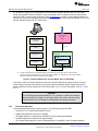
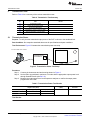
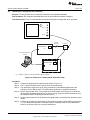
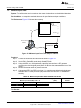
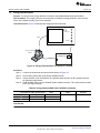
Application Report
SWRA370 – August 2011
Basic RF Testing of CCxxxx Devices
Abhishek Chattopadhyay
.................................................................................. Low-Power RF Products
ABSTRACT
This document presents users of Texas Instruments' low-power RF products with an overview of the
different characterization tests (conducted, not radiated) that are performed during the device verification
process. The document covers the basic setup of the test system and gives procedural information about
each test.
Throughout this document, the term CCxxxx refers to the low-power CC25xx, CC11xx, CC10XX, and
CC24xx RF device families.
Keywords:
• RF Testing
• RX Test
• Conformance Testing
• Output Power
• SmartRF Studio
• TX Test
• Characterization Test
• Sensitivity
SmartRF is a trademark of Texas Instruments.
Apple, Macintosh are registered trademarks of Apple Inc.
Bluetooth is a registered trademark of Bluetooth SIG.
Linux is a registered trademark of Linus Torvalds.
Microsoft, Windows are registered trademarks of Microsoft Corporation.
LabVIEW is a trademark of National Instruments.
ZigBee is a registered trademark of Zigbee Alliance.
All other trademarks are the property of their respective owners.
SWRA370 – August 2011
Submit Documentation Feedback
Basic RF Testing of CCxxxx Devices
Copyright © 2011, Texas Instruments Incorporated
1
www.ti.com
Contents
Introduction .................................................................................................................. 4
1.1
Abbreviations ....................................................................................................... 4
2
Standards and System Requirements ................................................................................... 5
2.1
Standards ........................................................................................................... 5
2.2
Test Equipment Suppliers ........................................................................................ 5
2.3
Test System Requirements ....................................................................................... 5
3
Frequency Correction ...................................................................................................... 9
4
DUT and Test Instrument Information .................................................................................. 11
4.1
DUT ................................................................................................................ 11
4.2
Test Instruments .................................................................................................. 11
5
Transmission Tests ........................................................................................................ 12
5.1
Transmission Power ............................................................................................. 12
5.2
Power Spectral Density Mask ................................................................................... 13
5.3
Error Vector Magnitude .......................................................................................... 14
5.4
Transmission Center Frequency Offset ....................................................................... 15
5.5
Spurious Emissions .............................................................................................. 16
6
Receive Testing Without LabVIEW ..................................................................................... 17
6.1
Receiver Sensitivity .............................................................................................. 17
6.2
Interference Testing .............................................................................................. 18
6.3
Interference Testing with RF Generator ....................................................................... 20
7
Receive Testing with LabVIEW .......................................................................................... 22
7.1
Receiver Sensitivity .............................................................................................. 22
7.2
Maximum Input Power ........................................................................................... 24
7.3
Adjacent/Alternate Channel ..................................................................................... 25
7.4
Energy Detection/RSSI .......................................................................................... 28
8
Electrical Tests ............................................................................................................. 29
8.1
Standby Mode ..................................................................................................... 30
8.2
Idle Mode .......................................................................................................... 30
8.3
Power-Down Mode ............................................................................................... 30
8.4
TX Mode ........................................................................................................... 30
8.5
RX Mode ........................................................................................................... 30
9
Testing Reminders ........................................................................................................ 31
10
References ................................................................................................................. 32
Appendix A
Offset EVM vs. EVM ............................................................................................. 33
1
List of Figures
2
................................................................................
1
Interface Between PC and CCxxxx EMs
2
Interface Between PC and Any Board with TI LPRF Radio ........................................................... 8
3
Transmission Power Test Setup......................................................................................... 12
4
Power Spectral Density Mask Requirements .......................................................................... 13
5
Power Spectral Density Mask Test Setup .............................................................................. 13
6
Error Vector Magnitude ................................................................................................... 14
7
EVM and Related Quantities ............................................................................................. 14
8
Error Vector Magnitude Test Setup ..................................................................................... 14
9
Transmission Center Frequency Offset Test Setup................................................................... 15
10
Spurious Emissions Test Setup ......................................................................................... 16
11
Receiver Sensitivity Test Setup
12
Interference Testing Setup ............................................................................................... 18
13
Interference Testing with RF Generator Setup ........................................................................ 20
14
Receiver Sensitivity Test Setup for LabVIEW ......................................................................... 22
15
Maximum Input Power Test Setup for LabVIEW ...................................................................... 24
16
IEEE 802.15.4 Standard for Adjacent/Alternate Channels ........................................................... 25
.........................................................................................
Basic RF Testing of CCxxxx Devices
Copyright © 2011, Texas Instruments Incorporated
7
17
SWRA370 – August 2011
Submit Documentation Feedback
www.ti.com
17
Adjacent/Alternate Channels Test Setup for LabVIEW ............................................................... 26
18
Energy Detection/RSSI Test Setup for LabVIEW ..................................................................... 28
19
Hardware Test Setup for LabVIEW ..................................................................................... 29
1
Terms and Abbreviations
List of Tables
2
3
4
5
6
7
8
9
10
11
12
13
14
15
16
17
18
19
20
21
22
23
24
25
26
27
28
..................................................................................................
DUT Information ...........................................................................................................
Test Instrument Information ..............................................................................................
Transmission Test Summary.............................................................................................
Transmission Power Test Results .......................................................................................
IEEE 802.15.4 Standards Requirements (Example) ..................................................................
Power Spectral Density Mask Test Results ............................................................................
Error Vector Magnitude Test Results ...................................................................................
Transmission Center Frequency Offset Test Results.................................................................
Spurious Emission Test Results .........................................................................................
Receive Test (without LabVIEW) Summary ...........................................................................
Receiver Sensitivity Test Results .......................................................................................
Adjacent Channel Test Results ..........................................................................................
Alternate Channel Test Results .........................................................................................
Adjacent Channel Test Results ..........................................................................................
Alternate Channel Test Results .........................................................................................
Receive Test with LabVIEW Summary .................................................................................
Receiver Sensitivity with LabVIEW Test Results ......................................................................
Maximum Input Power with LabVIEW Test Results ..................................................................
Adjacent Channel with LabVIEW Test Results ........................................................................
Alternate Channel with LabVIEW Test Results ........................................................................
Energy Detection/RSSI with LabVIEW Test Results .................................................................
Hardware Tests with LabVIEW Summary ..............................................................................
Standby Mode Test Results with LabVIEW ............................................................................
Idle Mode Test Results with LabVIEW .................................................................................
Power-Down Mode Test Results with LabVIEW ......................................................................
TX Mode Test Results with LabVIEW ..................................................................................
RX Mode Test Results with LabVIEW ..................................................................................
SWRA370 – August 2011
Submit Documentation Feedback
Basic RF Testing of CCxxxx Devices
Copyright © 2011, Texas Instruments Incorporated
4
11
11
12
12
13
13
14
15
16
17
18
19
19
21
21
22
23
24
27
27
28
29
30
30
30
30
30
3
Introduction
1
www.ti.com
Introduction
This document provides the user of Texas Instruments' low-power RF products with an overview of the
different characterization tests (conducted, not radiated) that are performed during the device verification
process. This descriptive document enables users to have a better understanding of the systems and
functions, and also presents general information about device testing under various conditions and
parameters. The document covers the basic setup of the test system and gives procedural information
about each test.
Texas Instruments’ low-power RF products make it easier to build wireless links for remote control,
metering, and sensing applications. In most cases, they are used inside unlicensed, or license-free,
wireless products. Unlicensed means only that the user of these products does not need an individual
license from the telecommunication regulatory authorities. Unlicensed does not mean unregulated; the
wireless product itself must usually meet strict regulations and be certified by the appropriate regulatory
authorities. The different international regulatory authorities such as the FCC, ETSI, and ARIB regulate the
use of radio receivers and transmitters. These bodies maintain specifications that must be met by all
devices for each of the tests mentioned in the application report. Refer to the respective standards
document (see Section 2.1).
1.1
Abbreviations
Table 1 lists many of the terms and abbreviations used in this document.
Table 1. Terms and Abbreviations
Abbreviation/Acronym
ARIB
CEBAL
Chipcon Evaluation Board Access Layer
dBm
Power ratio in decibels (dB) of the measured power
referenced to 1 mW
DUT
Device under test
EB
Evaluation board
EM
Evaluation module
ETSI
European Telecommunications Standards Institute
EVM
Error vector magnitude
FCC
Federal Communications Commission
FSQ
Full spectrum quantization
GUI
Graphical user interface
IEEE
Institute of Electrical and Electronics Engineer
INT
Interference source, interference signal
ISM
Industrial, scientific, medical
MSK
Minimum shift keying
PER
Packet error rate
PSD
Power spectral density
RSSI
Received signal strength indicator
RX
4
Definition/Meaning
Association of Radio Industries and Businesses
Receive, receiver
SMA
Sub Miniature version A connector
SoC
System on chip
SPI
Serial parallel interface
TX
Transmit, transmission, transmitter
Basic RF Testing of CCxxxx Devices
Copyright © 2011, Texas Instruments Incorporated
SWRA370 – August 2011
Submit Documentation Feedback
Standards and System Requirements
www.ti.com
2
Standards and System Requirements
2.1
Standards
The following standards serve as references for the tests described in this document. All electronic links
are current at the time of document publication.
• Bluetooth® Low Energy RF PHY Standard
• ZigBee® RF4CE Standard
• Zigbee Standard
• FCC, Section 47CFR15 – Part 15 Standard
• ETSI EN 300 440 Standard
• ETSI EN 300 220 Standard
• IEEE 802.15.4 Standard
• ARIB T-66 Standard
2.2
Test Equipment Suppliers
The different test equipment used to perform the various procedures described in this document can be
procured from the following suppliers. Obtaining some of this equipment may require going through an
agent. All electronic links are current at the time of document publication.
• Rohde & Schwarz
• Agilent
• Anritsu
• Tektronix
• Test Equity
• National Instruments
2.3
Test System Requirements
Any characterization test system has some generic components and additional specialty engineering
customization. A typical test system generally consists of these components and subsystems:
• Signal analyzers (spectrum analyzers): These tools are widely used to measure the frequency
response, noise, and distortion characteristics of all types of RF circuitry. These devices compare the
input and output spectra under a variety of conditions. A typical test system usually requires only one
signal analyzer.
• Signal generators: These devices generate repeating or non-repeating electronic signals (in either the
analog or digital domain). A typical system should have at least two signal generators: one to generate
the primary signal, the second to generate an interference signal. The CC devices from TI can be used
as a signal source in some lab setups. However, the power resolution may not be as good as that
produced by a signal generator.
• Temperature chamber: An enclosure used to test the effects of specified temperature conditions on a
series of test devices. A single temperature chamber should be sufficient for most test systems.
• Connectors/cables/splitters: These components connect different signals using coaxial cable from
the test system to (and from) the device under test (DUT).
• LabVIEW™: LabVIEW, or Laboratory Virtual Instrumentation Engineering Workbench, is a software
platform and development environment for a visual programming language from National Instruments.
The graphical language is named G. Originally released for the Apple® Macintosh® in 1986, LabVIEW
is commonly used for data acquisition, instrument control, and industrial automation on a variety of
platforms including Microsoft® Windows®, various versions of Unix, Linux®, and Mac OS X. This
software is used as a platform to automate the entire test system.
• SmartRF™ Studio: SmartRF Studio (see Ref. 10) is a Windows-based application that can be used to
evaluate and configure low-power RF ICs from Texas Instruments. This tool helps RF system
designers to quickly and easily evaluate the respective devices at an early stage in the design process.
It is especially useful for generation of configuration register values, for practical testing of the RF
SWRA370 – August 2011
Submit Documentation Feedback
Basic RF Testing of CCxxxx Devices
Copyright © 2011, Texas Instruments Incorporated
5
Standards and System Requirements
•
•
www.ti.com
system, and for finding optimized external component values. SmartRF Studio can be used either as a
standalone application or together with some evaluation boards that are shipped in RF IC development
kits.
Network analyzer (vector network analyzer): This tool is an instrument that measures the network
parameters of electrical networks. Contemporary network analyzers usually measure s- parameters
because reflection and transmission of electrical networks are easy to measure at high frequencies,
but there are other network parameter sets such as y-parameters, z-parameters, and h-parameters.
Network analyzers are often used to characterize two-port networks such as amplifiers and filters; they
can also be used on networks with an arbitrary number of ports. It is useful to have one network
analyzer available.
Oscilloscope: This electronic test instrument allows users to observe constantly varying signal
voltages, usually as a two-dimensional graph of one or more electrical potential differences with a
vertical or Y axis, plotted as a function of time (horizontal or x axis). Although an oscilloscope displays
voltage on the vertical axis, any other quantity that can be converted to a voltage can be displayed as
well. In most instances, oscilloscopes show events that repeat with either no change or that change
slowly. Having an oscilloscope is useful for a test system.
The more equipment one has in the test configuration, the greater need there is to automate the various
testing processes. For an elaborate setup, then, one should use a platform such as LabVIEW and write
specific application routines to enable the different test equipment to interface together.
Keep in mind that the capabilities of the available equipment used in a given test system will likely limit the
types of testing that can be performed.
2.3.1
System Setup
This document describes two types of test system configurations: without LabVIEW and with LabVIEW.
This section briefly describes each configuration.
2.3.1.1
Manual Test Systems (Without LabVIEW)
Systems not using LabVIEW use the following test equipment and resources:
1. CCxxxx Evaluation Module
2. SmartRF Evaluation Board (one)
3. Male to Male SMA RF cable
4. Variable attenuators (two)
5. PC with SmartRF Studio software installed
6. RF coupler (combiner)
7. RF signal generator (two)
8. Signal analyzer
2.3.1.2
Automatic Test Systems (Using LabVIEW)
Systems using LabVIEW use the following test equipment and resources:
1. CCxxxx Evaluation Module
2. SmartRF Evaluation Board (one)
3. Male to Male SMA RF cable
4. Signal analyzer
5. PC with SmartRF Studio and LabVIEW software installed
6. RF coupler (combiner)
7. RF signal generator (two)
6
Basic RF Testing of CCxxxx Devices
Copyright © 2011, Texas Instruments Incorporated
SWRA370 – August 2011
Submit Documentation Feedback
Standards and System Requirements
www.ti.com
2.3.2
Initial Conditions for Testing
The device under test (DUT) is connected to the tester via a 50-Ω connector. If there is no antenna
interface, a temporary 50-Ω interface or a suitable coupling device (50-Ω load) should be used.
For RX testing, the input reference signal (both as the desired signal and the interference signal) should
have certain characteristics that must be set according to the respective standards document.
Payload content of the desired signal should be a sequence specified by the relevant standard. It must be
identical for all transmitted packets.
In test cases where an interference signal is used, the interference signal characteristics must be defined
by the applicable standards for which the device is being evaluated.
2.3.3
System Communication Overview
The user can communicate with the DUT using SmartRF Studio 7/LabVIEW. These programs
communicates with the evaluation board over the USB interface via the(Chipcon Evaluation Board Access
Layer (CEBAL). This software library contains all the functions required to control the radio device on the
EB. Figure 1 illustrates the connection between a PC and the SmartRF EB.
PC
SmartRF Evaluation Board
SmartRF Studio/
LabVIEW
CCxxxx Transceiver/
CCxxxx SoC
SPI/
Debug Interface
CEBAL
USB MCU
Windows OS
SmartRF Eval Board
Firmware
USB Driver
USB
Cable
Figure 1. Interface Between PC and CCxxxx EMs
For proper operation of the applications that use CEBAL, the board must have compatible firmware that
runs on the USB MCU. If the firmware is out-of-date, SmartRF Studio 7 proposes that the user update the
firmware. The firmware update can be done directly in SmartRF Studio 7.
SWRA370 – August 2011
Submit Documentation Feedback
Basic RF Testing of CCxxxx Devices
Copyright © 2011, Texas Instruments Incorporated
7
Standards and System Requirements
www.ti.com
It is possible to connect your own hardware to the SmartRF Evaluation Board to test your own radio
design with SmartRF Studio7/LabVIEW. Connect the board to the TI evaluation board via the breakout
pins on the EB, or use the target connector on the CC Debugger. For SoCs, use the debug interface; for
transceivers, use the serial peripheral interface (SPI). Figure 2 shows the connection between a PC and a
generic evaluation board with a TI LPRF radio.
Any board with
TI LPRF
Radio
PC
SmartRF Studio/
LabVIEW
Note (1)
CEBAL
SmartRF Evaluation Board or
CC Debugger
Windows OS
USB MCU
CEBAL Firmware
USB Driver
USB
Cable
(1)
Connect the board to the TI evaluation board via the break-out pins on the board, or user the target
connector on the CC Debugger. For SoCs, use the debug interface; for transceivers, use the SPI interface.
Refer to the evaluation board user guide for more details.
Figure 2. Interface Between PC and Any Board with TI LPRF Radio
In all cases, make sure that the boards are properly connected and that the voltage levels are correct.
These cautions are especially relevant if you are not using level shifters and the voltage level on your
board is different from the voltage level on the EB (usually 3.3 V). For more information, see Ref. 11 and
Ref. 12.
CAUTION
The CC Debugger operates internally at 3.3 V. However, it has level converters
that will detect the voltage on the target board and ensure that the debug
control lines are set to a voltage that corresponds to the target I/O voltage.
2.3.4
Test System Operation
Use these general parameters to perform tests in TX mode when using LabVIEW:
• Set the DUT to TX mode using SmartRF Studio 7.
• Supply and temperature are set by LabVIEW.
• The signal analyzer is configured by LabVIEW to measure the transmitted data.
• LabVIEW captures the data from the signal analyzer.
• The collected information then can be interpreted either in LabVIEW or other PC-based software.
8
Basic RF Testing of CCxxxx Devices
Copyright © 2011, Texas Instruments Incorporated
SWRA370 – August 2011
Submit Documentation Feedback
Frequency Correction
www.ti.com
Use these general parameters to perform tests in RX mode when using LabVIEW:
• Set the DUT to RX mode using SmartRF Studio 7.
• Supply/temperature are set by LabVIEW.
• The signal analyzer is configured by LabVIEW to transmit data continuously or in packets that adhere
to standards.
• SmartRF Studio 7/LabVIEW captures the data from the DUT.
• This collected information then can be interpreted either in LabVIEW or exported to other PC-based
software.
3
Frequency Correction
Electronic circuits often use the mechanical resonance of a vibrating piezoelectric crystal to create an
electrical signal with a very precise frequency. This frequency is commonly used to provide a stable clock
signal for digital integrated circuits and to stabilize frequencies for radio transmitters and receivers.
Environmental changes in temperature, humidity, pressure, and external vibration can change the
resonant frequency of a crystal. The age of a crystal also adds inaccuracies to the crystal over time.
Because there is always some inaccuracy in the crystals used with radios, one way to correct for this error
is required in order to obtain an accurate measurement of sensitivity and other parameters.
The carrier frequency in the chip is mathematically related to the crystal frequency. For example, for the
CC2500 the carrier frequency is calculated as shown by Equation 1:
f
fCARRIER = XOSC
· FREQ[23:0]
216
(1)
(
(
Where FREQ[23:0] is the base frequency for the frequency synthesizer in increments of
fXOSC
216
However, the actual crystal frequency is not the same as the stated crystal frequency as a result of the
inaccuracies noted earlier. Consequently, we must calculate the actual crystal frequency.
After putting the device into unmodulated, continuous TX mode with the settings found using SmartRF
Studio, use a spectrum analyzer to measure the exact carrier frequency coming out of the chip.
This measured frequency is then put into Equation 1 from the product data sheet, and one solves for fXOSC.
This result is the actual crystal frequency for the specific DUT that can then be used to determine the
exact carrier frequency across the band.
In the CC253x/CC254x devices, the FREQTUNE register is used to tune the crystal oscillator. The default
setting '1111' leaves the XOSC not tuned. Changing the setting from default switches in extra capacitance
to the oscillator, effectively lowering the XOSC frequency. As a result, the final crystal frequency can be
controlled by adjusting the value of the FREQTUNE register in these devices.
SWRA370 – August 2011
Submit Documentation Feedback
Basic RF Testing of CCxxxx Devices
Copyright © 2011, Texas Instruments Incorporated
9
Frequency Correction
www.ti.com
Example 1.
Calculate the actual crystal frequency for a particular carrier frequency based on the known crystal frequency.
Assume a 26-MHz crystal for a CC2500 device. The carrier frequency is set to 2.4 GHz using these register
settings:
• FREQ2 [23:16] = 0x5C
• FREQ1 [15:8] = 0x4E
• FREQ0 [7:0] = 0xC4
• FREQ [23:0] = 0x5C4EC4
• FREQ = 6049476 [hex to dec conversion]
If the measured carrier frequency is 2.41 GHz, then the actual crystal frequency can be calculated using
Equation 1.
Solving for fXOSC produces these results:
16
f
·2
fXOSC = CARRIER
FREQ[23:0]
16
(
·
(
fXOSC
(
GHz 2
=
(2.416049476
fXOSC = 26.108 MHz
Even though the crystal is rated at 26 MHz, as a result of inaccuracies the actual crystal frequency is
26.108 MHz. Therefore, the signal generator and signal analyzer must be set to frequencies calibrated from
the true crystal frequency.
10
Basic RF Testing of CCxxxx Devices
Copyright © 2011, Texas Instruments Incorporated
SWRA370 – August 2011
Submit Documentation Feedback
DUT and Test Instrument Information
www.ti.com
4
DUT and Test Instrument Information
This page (and subsequent pages) can be printed and used as a record for the details of the respective
test setup.
4.1
DUT
Table 2 shows the generic DUT information.
Table 2. DUT Information
Product
Model Name
Hardware Version
Host Interface Type
Module SN
4.2
Test Instruments
Table 3 lists the general test instrument data. (See Section 2.3 for more information.)
Table 3. Test Instrument Information
Item
Vendor
Model Name
Quantity
Signal generator
Power combiner
Spectrum analyzer
Power meter
Attenuator
Temperature chamber
Oscilloscope
Network analyzer
SWRA370 – August 2011
Submit Documentation Feedback
Basic RF Testing of CCxxxx Devices
Copyright © 2011, Texas Instruments Incorporated
11
Transmission Tests
5
www.ti.com
Transmission Tests
Refer to Table 4 for a summary of the various transmission tests.
Table 4. Transmission Test Summary
Section
No
5.1
Item
Result
5.1
Transmission Power
5.2
Power Spectral Density Mask
5.3
Error Vector Magnitude
5.4
Transmission Center Frequency Offset
5.5
Spurious Emissions on Transmission
Transmission Power
Purpose: To verify that the transmitted output power of the DUT conforms to the standards limit.
Pass Condition: See respective standards document for specifications and pass conditions.
Test Environment: Figure 3 illustrates the transmission power test setup.
Spectrum Analyzer
PC with SmartRF Studio installed
SmartRF Eval Board
and Eval Module
Figure 3. Transmission Power Test Setup
Procedure:
Step 1. Connect the instruments and test board as shown in Figure 3.
Step 2. Set the EM to unmodulated, continuous TX mode with the appropriate output power level
through SmartRF Studio (see Ref. 10).
Step 3. Measure the output power level on the spectrum analyzer to confirm the output power
programmed on the EM.
Table 5. Transmission Power Test Results
Design Specification
(dBm)
Output Power (dBm)
Freq 1 (MHz)
Freq 2 (MHz)
Pass/Fail?
Freq 3 (MHz)
xx
xx
Test Results:
12
Basic RF Testing of CCxxxx Devices
Copyright © 2011, Texas Instruments Incorporated
SWRA370 – August 2011
Submit Documentation Feedback
Transmission Tests
www.ti.com
5.2
Power Spectral Density Mask
Purpose: To verify that the PSD of the DUT is able to conform to stated conformance limits.
Pass Condition: Refer to the respective standards document. Table 6 shows an example for the IEEE
802.15.4 standards requirements. Figure 4 illustrates the requirements.
Table 6. IEEE 802.15.4 Standards Requirements (Example)
Frequency
Relative Limit
Absolute Limit
|f – fC| > 3.5 MHz
–20 dB
–30 dBm
100 kHz
-20 dB or more
-30 dBm or less
2450
2455
2458.5
2460
MHz
3.5 MHz
Figure 4. Power Spectral Density Mask Requirements
Test Environment: Figure 5 shows the test setup.
Spectrum Analyzer
PC with SmartRF Studio installed
SmartRF Eval Board
and Eval Module
Figure 5. Power Spectral Density Mask Test Setup
Procedure:
Step 1. Connect the instruments and test board as shown in Figure 5.
Step 2. Set the EM to continuous TX mode through SmartRF Studio.
Step 3. Verify that the PSD mask conforms to the given standard on the spectrum analyzer.
Table 7. Power Spectral Density Mask Test Results
Design Specification
(%)
PSD Relative Limit (%)
Freq 1 (MHz)
Freq 2 (MHz)
Pass/Fail?
Freq 3 (MHz)
xx
xx
Test Results:
SWRA370 – August 2011
Submit Documentation Feedback
Basic RF Testing of CCxxxx Devices
Copyright © 2011, Texas Instruments Incorporated
13
Transmission Tests
5.3
www.ti.com
Error Vector Magnitude
Purpose: Transmission modulation accuracy is measured using error vector magnitude (EVM). EVM, as
illustrated in Figure 6 and Figure 7, is the magnitude of the phase difference as a function of time between
an ideal reference signal and the measured transmitted signal.
Q
Magnitude Error
(IQ Error Magnitude)
Q
Range of
Worst-Case
Error
Ideal
Constellation
Point
Error
Vector
Measured
Signal
I
Measured
Point
Ideal (Reference)
Signal
f
Error
Vector
Phase Error
(IQ Error Phase)
I
Figure 6. Error Vector Magnitude
Figure 7. EVM and Related Quantities
Pass Condition: See the respective standards document for specifications and pass conditions.
Test Environment: Figure 8 illustrates the setup for the EVM test.
Spectrum Analyzer
PC with SmartRF Studio installed
SmartRF Eval Board
and Eval Module
Figure 8. Error Vector Magnitude Test Setup
Procedure:
Step 1. Connect the instruments and test board as shown in Figure 8.
Step 2. Set the EM to continuous TX mode with random modulated data through SmartRF Studio.
Step 3. Measure EVM with the spectrum analyzer after setting up the instrument by following the
steps described in the tool user manual. (See Appendix A for more information.)
Example: EVM measurements on ZigBee signals using a Rohde & Schwarz FSQ can be set up
following the instructions in Ref. 2.
Table 8. Error Vector Magnitude Test Results
Design Specification
(%)
EVM (%) at ____ kbp/s
Freq 1 (MHz)
Freq 2 (MHz)
Pass/Fail?
Freq 3 (MHz)
xx
xx
Test Results:
14
Basic RF Testing of CCxxxx Devices
Copyright © 2011, Texas Instruments Incorporated
SWRA370 – August 2011
Submit Documentation Feedback
Transmission Tests
www.ti.com
5.4
Transmission Center Frequency Offset
Purpose: To verify that the center frequency offset is within limits.
Pass Condition: See respective standards document for specifications and pass conditions.
Test Environment: Figure 9 shows the setup for center frequency offset transmission testing.
Spectrum Analyzer
PC with SmartRF Studio installed
SmartRF Eval Board
and Eval Module
Figure 9. Transmission Center Frequency Offset Test Setup
Procedure:
Step 1. Connect the instruments and test board as shown in Figure 9.
Step 2. Set the EM to continuous TX mode through SmartRF Studio.
Step 3. Set the center frequency to the desired channel frequency; ensure that the signal is not
modulated.
Step 4. Measure the actual frequency on the spectrum analyzer. The difference between the actual
frequency and the center frequency is the frequency offset.
Table 9. Transmission Center Frequency Offset Test Results
Channel
Frequency
Frequency Offset
Design Specification
(ppm)
Pass/Fail?
xx
xx
xx
Test Results:
SWRA370 – August 2011
Submit Documentation Feedback
Basic RF Testing of CCxxxx Devices
Copyright © 2011, Texas Instruments Incorporated
15
Transmission Tests
5.5
www.ti.com
Spurious Emissions
Purpose: To verify that the conducted spurious emissions are within limits.
Pass Condition: See respective standards document for specifications and pass conditions.
Test Environment: Figure 10 illustrates the spurious emissions test setup.
Spectrum Analyzer
PC with SmartRF Studio installed
SmartRF Eval Board
and Eval Module
Figure 10. Spurious Emissions Test Setup
Procedure:
Step 1. Connect the instruments and test board as shown in Figure 10.
Step 2. Set the EM to continuous TX mode with random modulated data through SmartRF Studio.
Set the center frequency to the desired channel frequency.
Step 3. Measure spurs from the minimum limit to the maximum limit of the spectrum analyzer.
Note that different spectrum analyzers have different maximum frequencies. Up to 25 GHz is more
than sufficient.
Table 10. Spurious Emission Test Results
Channel
Frequency
Measured Spur
Design Specification
Pass/Fail?
xx
xx
xx
Test Results:
16
Basic RF Testing of CCxxxx Devices
Copyright © 2011, Texas Instruments Incorporated
SWRA370 – August 2011
Submit Documentation Feedback
Receive Testing Without LabVIEW
www.ti.com
6
Receive Testing Without LabVIEW
Refer to Table 11 for a summary of the various receiver tests to be performed without using LabVIEW.
Table 11. Receive Test (without LabVIEW) Summary
Section
No
6.1
Item
Result
6.1
Receiver Sensitivity
6.2
Interference Testing
6.3
Interference Testing with Signal Generator
Receiver Sensitivity
CAUTION
One issue to remember with the configuration described here is that RF power
can reach the receiver outside the path through the coaxial cable and
attenuators. This issue is of greater concern if the two boards are placed very
close together and the receiver is operated with very good sensitivity (that is,
low data rate and receiver bandwidth). This problem is observed if the receiver
can decode packets even with very high attenuation, and it is not possible to
find the sensitivity threshold correctly. To avoid this problem, one of the boards
should be placed in a shielded box where the shield is grounded, and the only
opening in the box is a small hole for cables to exit. This configuration reduces
radiation to a minimum.
Purpose: To verify that the receiver sensitivity conforms to performance standards.
Pass Condition: See respective standards document for specifications and pass conditions.
Test Environment: Figure 11 illustrates the test setup for receiver sensitivity.
Variable
Attenuator
SmartRF Eval Board
and Eval Module
TX
PC with SmartRF Studio
installed
SmartRF Eval Board
and Eval Module
RX
Shielded Box
Figure 11. Receiver Sensitivity Test Setup
SWRA370 – August 2011
Submit Documentation Feedback
Basic RF Testing of CCxxxx Devices
Copyright © 2011, Texas Instruments Incorporated
17
Receive Testing Without LabVIEW
www.ti.com
Procedure:
Step 1. Connect the instruments and test board as shown in Figure 11.
Step 2. Configure both the TX side and the RX side with the appropriate RF settings. Select the
packet TX or packet RX tab, and select an appropriate packet format.
Step 3. Start up the receivers first. Ensure that the Seq number included in payload box is checked
(enabled).
Step 4. Start the transmitter by clicking Start.
Step 5. The RSSI readout on the RX side provides a relative indicator of the signal strength
Step 6. The PER is calculated using this formula:
PER % = (No of packets lost/Total number of packets) x 100
Step 7. Increase the attenuation until the PER reaches 1%. This level defines the sensitivity
threshold.
Table 12. Receiver Sensitivity Test Results
Design Specification
(dBm)
Sensitivity (dBm), PER < 1%
Freq 1 (MHz)
Freq 2 (MHz)
Pass/Fail?
Freq 3 (MHz)
xx
xx
Test Results:
6.2
Interference Testing
Purpose: To verify that the receiver sensitivity conforms to the published standards.
Pass Condition: See respective standards document for specifications and pass conditions.
Test Environment: Figure 12 illustrates the interference test setup.
SmartRF Eval Board
and Eval Module
Variable
Attenuator
Interference
Source
Variable
Attenuator
SmartRF Eval Board
and Eval Module
Combiner
(1)
1 2
Sum
TX
PC with SmartRF Studio
installed
SmartRF Eval Board
and Eval Module
RX
Shielded Box
(1)
3-dB loss in signal on each input path through the combiner.
Figure 12. Interference Testing Setup
18
Basic RF Testing of CCxxxx Devices
Copyright © 2011, Texas Instruments Incorporated
SWRA370 – August 2011
Submit Documentation Feedback
Receive Testing Without LabVIEW
www.ti.com
Procedure:
Step 1. Connect the instruments and test board as shown in Figure 12.
Step 2. The TX and RX boards must be set up as for the sensitivity test.
Step 3. The INT (interference) signal is set up as for TX; however, the frequency can be different
than that of either the TX and RX signals, unless testing for co-channel interference.
Furthermore, unlike the TX that transmits packets, the INT transmits continuously (that is, it is
a continuous modulated signal).
Step 4. Set the output power of the TX such that the received power at the RX end is 10 dB above
the sensitivity threshold obtained from sensitivity testing. (Remove 10 dB of attenuation from
the attenuators after completing the sensitivity test.)
Step 5. Set the output power low for the INT initially, and perform the sensitivity test at the RX.
Step 6. Continue to increase the output power of the INT until the PER is greater than 1%. The
difference between the TX and INT power measured on the RX side indicates the ability of
the CCxxxx device to overcome interference.
Table 13. Adjacent Channel Test Results
Channel
Frequency (MHz)
Difference (dB)
Design Specification
(dB)
Pass/Fail?
xx
xx
xx
Table 14. Alternate Channel Test Results
Channel
Frequency (MHz)
Difference (dB)
Design Specification
(dB)
Pass/Fail?
xx
xx
xx
Test Results:
SWRA370 – August 2011
Submit Documentation Feedback
Basic RF Testing of CCxxxx Devices
Copyright © 2011, Texas Instruments Incorporated
19
Receive Testing Without LabVIEW
6.3
www.ti.com
Interference Testing with RF Generator
Purpose: To verify that the receiver sensitivity conforms to the published standards.
Pass Condition: See respective standards document for specifications and pass conditions.
Test Environment: Figure 13 illustrates the test setup for interference testing with an RF generator.
RF Generator
Ext 1 In
RF Out
Variable
Attenuator
SmartRF Eval Board
and Eval Module
Combiner
(1)
1 2
Sum
TX
PC with SmartRF Studio
installed
SmartRF Eval Board
and Eval Module
RX
Shielded Box
(1)
3-dB loss in signal on each input path through the combiner.
Figure 13. Interference Testing with RF Generator Setup
Procedure:
Step 1. Connect the instruments and test board as shown in Figure 13.
Step 2. The TX and RX boards must be set up as for the sensitivity test.
Step 3. The interference signal is set up by using a continuous, unmodulated signal where the
frequency can be different from TX and RX unless testing for co-channel interference.
Step 4. Set the output power of the TX such that the received power at the RX end is 10 dB above
the sensitivity threshold obtained from sensitivity testing. (Remove 10 dB of attenuation from
the attenuators after completing the sensitivity test.)
Step 5. Set the output power low for the interference signal initially, and perform the sensitivity test at
the RX.
Step 6. Continue to increase the output power of the interference signal until the PER is greater than
1%. The difference between the TX and INT power measured at the RX side indicates the
ability of the CCxxxx device to overcome interference.
20
Basic RF Testing of CCxxxx Devices
Copyright © 2011, Texas Instruments Incorporated
SWRA370 – August 2011
Submit Documentation Feedback
Receive Testing Without LabVIEW
www.ti.com
Table 15. Adjacent Channel Test Results
Channel
Frequency (MHz)
Difference (dB)
Design Specification
(dB)
Pass/Fail?
xx
xx
xx
Table 16. Alternate Channel Test Results
Channel
Frequency (MHz)
Difference (dB)
Design Specification
(dB)
Pass/Fail?
xx
xx
xx
Test Results:
SWRA370 – August 2011
Submit Documentation Feedback
Basic RF Testing of CCxxxx Devices
Copyright © 2011, Texas Instruments Incorporated
21
Receive Testing with LabVIEW
7
www.ti.com
Receive Testing with LabVIEW
Refer to Table 17 for a summary of the various receiver tests performed with LabVIEW.
Table 17. Receive Test with LabVIEW Summary
Section
No
7.1
Item
Result
7.1
Receiver Sensitivity
7.2
Maximum Input Power
7.3
Adjacent/Alternate Channel
7.4
Energy Detect
Receiver Sensitivity
Purpose: To verify that the receiver sensitivity conforms to the published standards.
Pass Condition: See respective standards document for specifications and pass conditions.
Test Environment: Figure 14 illustrates the test setup for receiver sensitivity with LabVIEW.
RF Generator
Ext 1 In
GPIB
RF Out
PC with LabView
installed
SmartRF Eval Board
and Eval Module
Figure 14. Receiver Sensitivity Test Setup for LabVIEW
22
Basic RF Testing of CCxxxx Devices
Copyright © 2011, Texas Instruments Incorporated
SWRA370 – August 2011
Submit Documentation Feedback
Receive Testing with LabVIEW
www.ti.com
Procedure:
Step 1. Connect the instruments and test board as shown in Figure 14.
Step 2. Set the EM in Packet RX mode through SmartRF Studio.
Step 3. Using LabVIEW, send 1000 packets at a specified data rate and modulation format from the
RF generator, while controlling the generator power. (Start 10 dB over the stated sensitivity of
the device.)
Step 4. Measure the actual number of packets received.
Step 5. Calculate the PER. If the PER is less than 1%, repeat the test with a reduced signal power.
When the PER ≥ 1%, the previous signal power with a PER less than 1% indicates the
sensitivity.
NOTE: See Ref. 3 for more detailed techniques to test TI CCxxxx devices for sensitivity.
Table 18. Receiver Sensitivity with LabVIEW Test Results
Design Specification
(dBm)
Sensitivity (dBm), PER < 1%
Freq 1 (MHz)
Freq 2 (MHz)
Pass/Fail?
Freq 3 (MHz)
xx
xx
Test Results:
SWRA370 – August 2011
Submit Documentation Feedback
Basic RF Testing of CCxxxx Devices
Copyright © 2011, Texas Instruments Incorporated
23
Receive Testing with LabVIEW
7.2
www.ti.com
Maximum Input Power
Purpose: To verify that the receiver maximum input power level conforms to the published data sheet
specifications.
Pass Condition: See respective standards document for specifications and pass conditions.
Test Environment: Figure 15 illustrates the test setup.
RF Generator
Ext 1 In
GPIB
RF Out
PC with LabView
installed
SmartRF Eval Board
and Eval Module
Figure 15. Maximum Input Power Test Setup for LabVIEW
Procedure:
Step 1. Connect the instruments and test board as shown in Figure 15.
Step 2. Set the EM in Packet RX mode through SmartRF Studio.
Step 3. Using LabVIEW, send 1000 packets at a specified data rate from the RF generator,
controlling the received signal power. (Start 10 dB below the stated saturation level of the
device.).
Step 4. Measure the actual number of packets received.
Step 5. Calculate the PER. If the PER is less than 1%, repeat the test with reduced signal power.
When the PER ≥ 1%, the previous signal power with a PER less than 1% indicates the
sensitivity.
Table 19. Maximum Input Power with LabVIEW Test Results
Maximum Input Power (dBm), PER < 1%
Freq 1 (MHz)
Freq 2 (MHz)
Design Specification
(dBm)
Pass/Fail?
Freq 3 (MHz)
xx
xx
Test Results:
24
Basic RF Testing of CCxxxx Devices
Copyright © 2011, Texas Instruments Incorporated
SWRA370 – August 2011
Submit Documentation Feedback
Receive Testing with LabVIEW
www.ti.com
7.3
Adjacent/Alternate Channel
Purpose: This test verifies that the minimum jamming resistance levels conforms to the published
standard.
Example 2.
Consider the 802.15.4 standards. The adjacent channel (Figure 16a) is one on either side of the desired
channel that is closest in frequency to the desired channel, and the alternate channel (Figure 16b) is one
channel removed from the adjacent channel.
Desired
Alternative
-52 dBm
30 dB
Adjacent
Desired
-82 dBm
-82 dBm
2450
2455
MHz
2450
(a)
2455
2460
MHz
(b)
Figure 16. IEEE 802.15.4 Standard for Adjacent/Alternate Channels
Pass Condition:
SWRA370 – August 2011
Submit Documentation Feedback
Adjacent Channel Rejection
Alternate Channel Rejection
0 dB
30 dB
Basic RF Testing of CCxxxx Devices
Copyright © 2011, Texas Instruments Incorporated
25
Receive Testing with LabVIEW
www.ti.com
Test Environment: Figure 17 illustrates the adjacent/alternate channel test setup for LabVIEW.
RF Generator
Ext 1 In
RF Out
RF Generator
Ext 1 In
RF Out
Combiner
(1)
GPIB
1 2
Sum
PC with LabView
installed
SmartRF Eval Board
and Eval Module
(1)
3-dB loss in signal on each input path through the combiner.
Figure 17. Adjacent/Alternate Channels Test Setup for LabVIEW
26
Basic RF Testing of CCxxxx Devices
Copyright © 2011, Texas Instruments Incorporated
SWRA370 – August 2011
Submit Documentation Feedback
Receive Testing with LabVIEW
www.ti.com
Procedure:
Step 1. Connect the instruments and test board as shown in Figure 17.
Step 2. Set the EM in Packet RX mode through SmartRF Studio.
Step 3. Set the output power of the first generator such that the received power at the EM end is at 3
dB greater than the minimum sensitivity obtained from sensitivity testing for LabVIEW.
Step 4. Using LabVIEW, send 1000 packets at a specified data rate from one of the RF generators,
controlling the received signal power.
Step 5. Using LabVIEW, set the frequency and power of the interference signal on the second
generator to the adjacent/alternate channel.
Step 6. Set the output power low for the interference signal (second generator) initially, then perform
the sensitivity test at the EM.
Step 7. Continue to increase the output power of the interference signal until the PER is greater than
1%. The difference in the first and second generator power (as seen on the EM side)
indicates the ability of the device to overcome interference, and is the adjacent/alternate
channel rejection.
Table 20. Adjacent Channel with LabVIEW Test Results
Channel
Frequency (MHz)
Difference (dB)
Design Specification
(dB)
Pass/Fail?
xx
xx
xx
Table 21. Alternate Channel with LabVIEW Test Results
Channel
Frequency (MHz)
Difference (dB)
Design Specification
(dB)
Pass/Fail?
xx
xx
xx
Test Results:
SWRA370 – August 2011
Submit Documentation Feedback
Basic RF Testing of CCxxxx Devices
Copyright © 2011, Texas Instruments Incorporated
27
Receive Testing with LabVIEW
7.4
www.ti.com
Energy Detection/RSSI
Purpose: To verify that the energy detection conforms to the published data sheet specifications.
Pass Condition: The mapping from the received power in decibels to energy detection value must be
linear, with a stated accuracy given in the standard.
Test Environment: Figure 18 illustrates the energy detection test setup.
RF Generator
Ext 1 In
GPIB
RF Out
PC with LabView
installed
SmartRF Eval Board
and Eval Module
Figure 18. Energy Detection/RSSI Test Setup for LabVIEW
Procedure:
Step 1. Connect the instruments and test board as shown in Figure 18.
Step 2. Set the EM in Packet RX mode through SmartRF Studio.
Step 3. Using LabVIEW, send 1000 packets at a specified data rate from the RF generator and set
the generator signal power.
Step 4. Read the RSSI value from the SmartRF Studio software interface. This value should correlate
to the sent signal strength.
Table 22. Energy Detection/RSSI with LabVIEW Test Results
Power Detection (dB) | Signal Strength = ____ (dBm)
Freq 1 (MHz)
Freq 2 (MHz)
Design Specification
(dBm)
Pass/Fail?
Freq 3 (MHz)
xx
xx
Test Results:
28
Basic RF Testing of CCxxxx Devices
Copyright © 2011, Texas Instruments Incorporated
SWRA370 – August 2011
Submit Documentation Feedback
Electrical Tests
www.ti.com
8
Electrical Tests
Table 23 summarizes the various electrical tests performed with LabVIEW.
Table 23. Hardware Tests with LabVIEW Summary
Section No
Item
8.1
Standby mode / RF disable mode
8.2
Idle mode
8.3
Power Down mode
8.4
TX mode
8.5
RX mode
Test Environment: Figure 19 illustrates the test setup for all hardware tests.
Multimeter
+
Power Supply
-
PC with SmartRF Studio installed
SoC BB and
Eval Mod
CC
Debugger
+
-
+
-
Figure 19. Hardware Test Setup for LabVIEW
Procedure:
Step 1.
Step 2.
Step 3.
Step 4.
Step 5.
Step 6.
Step 7.
Step 8.
Step 9.
Connect the instruments and test board as shown in Figure 19.
The test requires the use of a SoC BB for accurate measurement; see Ref. 14.
Mount the CCxxxx EM on the SoC BB.
Supply power to the board from an external supply rather than AA battery cells..
Connect a multimeter in series with the supply line.
Connect the CCDebugger (see Ref. 13) to the SoC BB to enable communication with the
CCxxxx EM.
Use SmartRF Studio to set the device to the proper modes.
Set the supply to 3.3 V.
Measure the current on the multimeter for each mode.
CAUTION
The CC Debugger influences the measurements. The debugger consumes
some current and increases the measured current going into the EM.
In particular, this device influences the sleep current measurements.
The debugger can be disconnected from the SoC BB after the device has been
set to the desired mode using SmartRF Studio. The radio device remains in the
active/sleep state, and it is possible to perform more accurate measurements.
A hot disconnect should not normally cause any damage to the devices.
SWRA370 – August 2011
Submit Documentation Feedback
Basic RF Testing of CCxxxx Devices
Copyright © 2011, Texas Instruments Incorporated
29
Electrical Tests
8.1
www.ti.com
Standby Mode
Table 24 lists the outcomes of the standby mode test.
Table 24. Standby Mode Test Results with LabVIEW
Voltage
Current (mA)
3.3 V
8.2
Idle Mode
Table 25 lists the outcomes of the idle mode test.
Table 25. Idle Mode Test Results with LabVIEW
Voltage
Current (mA)
3.3 V
8.3
Power-Down Mode
Table 26 lists the outcomes of the power-down mode test.
Table 26. Power-Down Mode Test Results with
LabVIEW
Voltage
Current (mA)
3.3 V
8.4
TX Mode
Table 27 lists the outcomes of the TX mode test.
Table 27. TX Mode Test Results with LabVIEW
8.5
Mode
Voltage
At 2.440 GHz (0 dBm)
3.3 V
Current (mA)
RX Mode
Table 28 lists the outcomes of the RX mode test.
Table 28. RX Mode Test Results with LabVIEW
Mode
Voltage
At 2.440 GHz (HG)
3.3 V
Current (mA)
At 2.440 GHz (LG)
30
Basic RF Testing of CCxxxx Devices
Copyright © 2011, Texas Instruments Incorporated
SWRA370 – August 2011
Submit Documentation Feedback
Testing Reminders
www.ti.com
9
Testing Reminders
These reminders are presented as general considerations for all users, regardless of the testing setup
used in a given situation.
1. The SMA cable connecting the EM to the signal analyzer should have a 50-Ω termination so it matches
with the 50 Ω of the SMA port from the EM.
2. The RX board must be shielded.
3. Good tests for the shielding while executing the sensitivity test are to increase the attenuation by 20 dB
to 40dB beyond the sensitivity stated in the product data sheet. If the RX is able to pick up the TX
signal, the shielding must be improved.
4. When performing these tests, it is better to keep the output power of the TX and INT radios at
approximately 0 dBm, and use attenuation provided by different attenuators.
5. In the interference signal setup, it is better to correlate the TX and INT outputs by simply turning off the
other output and checking the RSSI at the RX end. These tests should be performed with the
transmitters in continuous transmit mode.
6. RF couplers are asymmetric. The attenuation associated with the lossy path should be factored in. If a
splitter (that is, a combiner) is used, it should be symmetric with equal attenuation on both paths.
7. The interference signal should be in continuous transmit mode.
8. If the carrier is unmodulated, the resulting difference in output power between the TX and INT indicates
the blocking.
9. If the carrier is modulated, the resulting difference in output power between the TX and INT indicates
the selectivity.
10. The shielded box can be a biscuit tin box with a small hole for the cable.
11. SmartRF Studio can be used to change the frequency for running the different interference tests.
12. When testing interference on IEEE 802.15.4 systems using an RF generator, if a modulated carrier is
used, use a continuous MSK, 2-Mbps modulated carrier.
13. The adjacent channel rejection (ACR) measurement on IEEE 802.15.4 systems is described in Ref. 1.
14. Keep the cables/attenuators/connectors clean. Otherwise, losses in the cables can be excessive.
SWRA370 – August 2011
Submit Documentation Feedback
Basic RF Testing of CCxxxx Devices
Copyright © 2011, Texas Instruments Incorporated
31
References
10
www.ti.com
References
Unless otherwise indicated, the following references are available for download at the Texas Instruments
website (www.ti.com).
1. Wium, E. (2009). ACR measurements on IEEE 802.15.4 systems. Application report. Literature number
SWRA255.
2. EVM measurements on ZigBee signals. (2005). News from Rohde & Schwarz, 185:1. Product
information bulletin.
3. Engjom, M. (2006). Practical sensitivity testing. Application report. Literature number SWRA097.
4. European Telecommunications Standards Institute. European government regulatory commission.
5. Federal Communications Commission. U.S. government regulatory commission.
6. Association of Radio Industries and Businesses. Trade association website.
7. Evjen, P. M. (2003). SRD regulations for license free transceiver operation. Application report.
Literature number SWRA090.
8. Engjom, M. (2006). 2.4 GHz regulations. Application report. Literature number SWRA060.
9. Loy, M., Karingattil, R., and L. Williams. (Eds.). (2005) . ISM-band and short range device regulatory
compliance overview. Application report. Literature number SWRA048.
10. SmartRF Studio. Product folder at www.ti.com.
11. SmartRF05EB. User’s guide. Literature number SWRU210.
12. CC Debugger. User’s guide. Literature number SWRU197.
13. Debugger and Programmer for RF System-on-Chips. Product folder at www.ti.com.
14. Battery Board for Systems-on-Chip. Product folder at www.ti.com.
15. RF and System Basics. Electronic resource. http://www.circuitsage.com/.
16. Grini, D. (2006.) RF Basics, RF for Non-RF Engineers. Seminar presentation: MSP430 Advanced
Technical Conference. Literature number SLAP127.
32
Basic RF Testing of CCxxxx Devices
Copyright © 2011, Texas Instruments Incorporated
SWRA370 – August 2011
Submit Documentation Feedback
www.ti.com
Appendix A Offset EVM vs. EVM
Offset EVM and EVM are both measurements of error vector magnitude; in other words, how far from the
ideal position the actual signal position is.
The difference between offset EVM and EVM is when to obtain these measurements. In offset EVM
measurements, calculate the EVM for the in-phase (I) portion of the signal at the start of the symbol, and
the quadrature-phase (Q) portion at the middle of the symbol. Using this approach, users can obtain the
EVM at the actual decision points that the demodulator makes when trying to decode it. This method is
the correct way to measure EVM because it reflects the actual demodulator in the CCxxxx devices.
For a perfect signal, it does not matter if you use offset EVM or EVM. For spectrums where the I and Q
phases are more noisy in the respective transitions than at the decision points, performing a regular EVM
measurement gives you a poorer result, but does not affect the ability to receive the signal.
SWRA370 – August 2011
Submit Documentation Feedback
Basic RF Testing of CCxxxx Devices
Copyright © 2011, Texas Instruments Incorporated
33
IMPORTANT NOTICE
Texas Instruments Incorporated and its subsidiaries (TI) reserve the right to make corrections, modifications, enhancements, improvements,
and other changes to its products and services at any time and to discontinue any product or service without notice. Customers should
obtain the latest relevant information before placing orders and should verify that such information is current and complete. All products are
sold subject to TI’s terms and conditions of sale supplied at the time of order acknowledgment.
TI warrants performance of its hardware products to the specifications applicable at the time of sale in accordance with TI’s standard
warranty. Testing and other quality control techniques are used to the extent TI deems necessary to support this warranty. Except where
mandated by government requirements, testing of all parameters of each product is not necessarily performed.
TI assumes no liability for applications assistance or customer product design. Customers are responsible for their products and
applications using TI components. To minimize the risks associated with customer products and applications, customers should provide
adequate design and operating safeguards.
TI does not warrant or represent that any license, either express or implied, is granted under any TI patent right, copyright, mask work right,
or other TI intellectual property right relating to any combination, machine, or process in which TI products or services are used. Information
published by TI regarding third-party products or services does not constitute a license from TI to use such products or services or a
warranty or endorsement thereof. Use of such information may require a license from a third party under the patents or other intellectual
property of the third party, or a license from TI under the patents or other intellectual property of TI.
Reproduction of TI information in TI data books or data sheets is permissible only if reproduction is without alteration and is accompanied
by all associated warranties, conditions, limitations, and notices. Reproduction of this information with alteration is an unfair and deceptive
business practice. TI is not responsible or liable for such altered documentation. Information of third parties may be subject to additional
restrictions.
Resale of TI products or services with statements different from or beyond the parameters stated by TI for that product or service voids all
express and any implied warranties for the associated TI product or service and is an unfair and deceptive business practice. TI is not
responsible or liable for any such statements.
TI products are not authorized for use in safety-critical applications (such as life support) where a failure of the TI product would reasonably
be expected to cause severe personal injury or death, unless officers of the parties have executed an agreement specifically governing
such use. Buyers represent that they have all necessary expertise in the safety and regulatory ramifications of their applications, and
acknowledge and agree that they are solely responsible for all legal, regulatory and safety-related requirements concerning their products
and any use of TI products in such safety-critical applications, notwithstanding any applications-related information or support that may be
provided by TI. Further, Buyers must fully indemnify TI and its representatives against any damages arising out of the use of TI products in
such safety-critical applications.
TI products are neither designed nor intended for use in military/aerospace applications or environments unless the TI products are
specifically designated by TI as military-grade or "enhanced plastic." Only products designated by TI as military-grade meet military
specifications. Buyers acknowledge and agree that any such use of TI products which TI has not designated as military-grade is solely at
the Buyer's risk, and that they are solely responsible for compliance with all legal and regulatory requirements in connection with such use.
TI products are neither designed nor intended for use in automotive applications or environments unless the specific TI products are
designated by TI as compliant with ISO/TS 16949 requirements. Buyers acknowledge and agree that, if they use any non-designated
products in automotive applications, TI will not be responsible for any failure to meet such requirements.
Following are URLs where you can obtain information on other Texas Instruments products and application solutions:
Products
Applications
Audio
www.ti.com/audio
Communications and Telecom www.ti.com/communications
Amplifiers
amplifier.ti.com
Computers and Peripherals
www.ti.com/computers
Data Converters
dataconverter.ti.com
Consumer Electronics
www.ti.com/consumer-apps
DLP® Products
www.dlp.com
Energy and Lighting
www.ti.com/energy
DSP
dsp.ti.com
Industrial
www.ti.com/industrial
Clocks and Timers
www.ti.com/clocks
Medical
www.ti.com/medical
Interface
interface.ti.com
Security
www.ti.com/security
Logic
logic.ti.com
Space, Avionics and Defense
www.ti.com/space-avionics-defense
Power Mgmt
power.ti.com
Transportation and
Automotive
www.ti.com/automotive
Microcontrollers
microcontroller.ti.com
Video and Imaging
www.ti.com/video
RFID
www.ti-rfid.com
Wireless
www.ti.com/wireless-apps
RF/IF and ZigBee® Solutions
www.ti.com/lprf
TI E2E Community Home Page
e2e.ti.com
Mailing Address: Texas Instruments, Post Office Box 655303, Dallas, Texas 75265
Copyright © 2011, Texas Instruments Incorporated