1
Embedded Solutions
20F012N00 E3 – 2008-07-28
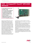
F12N – 3U CompactPCI®
MPC5200B SBC
Configuration example
User Manual
®
F12N – 3U CompactPCI® MPC5200B SBC
F12N – 3U CompactPCI® MPC5200B SBC
Equipped with the MPC5200B PowerPC®, the F12N single-board computer is a
versatile 3U Eurocard CompactPCI® board that operates at up to 400 MHz and 700
MIPS. The F12N is designed especially for systems which require low power
consumption and mechanical robustness. With the processor consuming less than 1
W, the board is delivered for -40 to +85°C operation temperature. All components
on the board are soldered. The F12N is thus well placed as a rugged computing
platform for mobile applications, offering the whole world of Linux based software
and real-time operating support for VxWorks® and QNX®.
The F12N is equipped with an on-board soldered SDRAM of up to 256 MB and up
to 1 GB NAND Flash as well as with 16 MB additional SDRAM, up to 8 MB boot
Flash and 2 MB battery-backed SRAM.
The SBC provides two Fast Ethernet interfaces, one serial line and USB 1.1 at its
front panel. As an alternative to RJ45, D-Sub connectors guarantee reliable
functions also in harsh environments. Two CAN controllers with V2.0A/B CAN
protocol are included in the MPC5200B and are accessible via SA-Adapters™. A
second serial interface can be accessed using an SA-Adapter™ on the F12N.
(E)IDE and GPIO are also on board.
The large FPGA on the F12N allows to realize additional user-defined functions
such as graphics, touch, further serial interfaces, further CAN bus controllers,
binary I/O etc. for the needs of the individual application in a very flexible way.
Before boot-up of the system, the FPGA is loaded from boot Flash. Updates of the
FPGA contents can be made inside the boot Flash during operation. The FPGA
functions can be physically implemented by using SA-Adapters™. A maximum of
8 SA-Adapters™ can be used on the F12N and I/O can be made accessible at the
front panel.
Equipped with a PCI-bridge chip, the F12N offers a full CompactPCI® interface
(system slot functionality) for reliable system expansion.
The F12N comes with MENMON™ support. This firmware/BIOS can be used for
bootstrapping operating systems (from disk, Flash or network), for hardware testing,
or for debugging applications without running any operating system.
MEN Mikro Elektronik GmbH
20F012N00 E3 – 2008-07-28
2
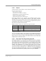
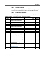
Technical Data
Technical Data
CPU
• PowerPC®
- MPC5200B
- Up to 400MHz
Memory
• 2x16KB L1 data and instruction cache integrated in MPC5200
• Up to 256MB SDRAM system memory
- Soldered DDR
- 64MHz memory bus frequency
• Up to 1GB soldered NAND Flash (and more), FPGA-controlled
• 16MB additional SDRAM, FPGA-controlled, e.g. for video data and NAND
Flash firmware
• Up to 8MB boot Flash
• 2MB GoldCap-backed SRAM, or: 128KB non-volatile FRAM
• Serial EEPROM 8kbits for factory settings
Mass Storage
• Parallel IDE (PATA)
- One IDE port via 44-pin on-board connector
- FPGA-controlled
- PIO mode 0 support
• Up to 1GB soldered ATA NAND Flash (and more), FPGA-controlled
I/O
• USB
- One USB 1.1 port
- Series A connector at front panel
- OHCI implementation
- Data rates up to 12Mbits/s
• Ethernet
- Two 10/100Base-T Ethernet channels
- One channel FPGA-controlled
- Two RJ45 or one D-Sub connector at front panel
• One RS232 UART (COM1)
- RJ45 or D-Sub connector at front panel
- Data rates up to 115.2kbits/s
- 512-byte transmit/receive buffer
- Handshake lines: CTS, RTS
• One UART (COM10)
- Accessible via I/O connector
- Physical interface at front panel using SA-Adapter™ via 10-pin ribbon cable
on I/O connector
- RS232..RS485, isolated or not: for free use in system (e. g. cable to front)
- Data rates up to 115.2kbits/s
- 16-byte transmit/receive buffer
- Handshake lines: CTS, RTS; DCD, DSR, DTR; RI
MEN Mikro Elektronik GmbH
20F012N00 E3 – 2008-07-28
3
Technical Data
• CAN bus
- Two CAN bus channels
- 2.0 A/B CAN protocol
- Data rates up to 1 Mbit/s
- Connection via on-board connectors
- External transceivers using SA-Adapters™
• GPIO
- 36 GPIO lines
- FPGA-controlled
- Connection via on-board I/O connector
• Further I/O depending on FPGA configuration
Front Connections (Standard)
• One USB 1.1 (Series A)
• Two Ethernet (RJ45)
• One RS232 UART (RJ45)
FPGA
• Standard factory FPGA configuration:
- Main bus interface
- 16Z070_IDEDISK - IDE controller for NAND Flash
- 16Z043_SDRAM - Additional SDRAM controller (16MB)
- 16Z023_IDENHS - IDE controller (PIO mode 0; non-hot-swap)
- 16Z087_ETH - Ethernet controller (10/100Base-T)
- 16Z025_UART - UART controller (controls COM10)
- 16Z034_GPIO - GPIO controller (40 lines, 5 IP cores)
• The FPGA offers the possibility to add customized I/O functionality. See FPGA.
Miscellaneous
•
•
•
•
Real-time clock with GoldCap backup
Power supervision and watchdog
Reset button, GPIO-controlled
Three user LEDs, GPIO-controlled; 1 FPGA power status LED
CompactPCI® Bus
•
•
•
•
Compliance with CompactPCI® Core Specification PICMG 2.0 R3.0
System slot
32-bit/32-MHz PCI-to-PCI bridge
V(I/O): +3.3V or +5V (Universal Board)
PXI™
• Four trigger lines compliant with PXI™ Specification R1.0
MEN Mikro Elektronik GmbH
20F012N00 E3 – 2008-07-28
4
Technical Data
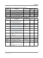
Electrical Specifications
• Supply voltage/power consumption, CompactPCI® standard version:
- +5V (-3%/+5%), 10mA max.
- +3.3V (-3%/+5%), 1A typ.
• Supply voltage/power consumption, stand-alone version:
- +5V (-3%/+5%), 800mA typ.
- Uses 5V only
• MTBF: 277,234h @ 40°C according to IEC/TR 62380 (RDF 2000)
Mechanical Specifications
• Dimensions: conforming to CompactPCI® specification for 3U boards
• Weight: 250g
Environmental Specifications
• Temperature range (operation):
- -40..+85°C (qualified components)
- Airflow: min. 10m³/h
• Temperature range (storage): -40..+85°C
• Relative humidity (operation): max. 95% non-condensing
• Relative humidity (storage): max. 95% non-condensing
• Altitude: -300m to + 3,000m
• Shock: 15g/11ms
• Bump: 10g/16ms
• Vibration (sinusoidal): 2g/10..150Hz
• Conformal coating on request
Safety
• PCB manufactured with a flammability rating of 94V-0 by UL recognized manufacturers
EMC
• Tested according to EN 55022 (radio disturbance), IEC1000-4-2 (ESD) and
IEC1000-4-4 (burst) with regard to CE conformity
BIOS
• MENMON™
Software Support
•
•
•
•
•
VxWorks®
Linux (ELinOS)
QNX®
CANopen firmware (Vector Informatik)
CAN support: MEN Driver Interface System (MDIS™ for Windows®, Linux,
VxWorks®, QNX®, OS-9®)
• For more information on supported operating system versions and drivers see
online data sheet.
MEN Mikro Elektronik GmbH
20F012N00 E3 – 2008-07-28
5
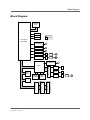
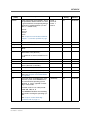
Block Diagram
Block Diagram
SDRAM
Main
EEPROM
RTC
F Front panel
B On-board
Watchdog
PowerPC®
MPC5200B
Ethernet
10/100Base-T
F
RS232 COM1
F
USB 1.1
F
CAN bus
B
SA
F
CAN bus
B
SA
F
I/O
Boot
Flash
SDRAM
Additional
NAND
Flash
F
IDE
B
GPIO
B
COM10
B
SA
F
CompactPCI® J1/J2
PCI-to-PCI Bridge
SRAM/
FRAM
PCI-104 P1
Multifunction external bus
FPGA
I/O Connector P2
Ethernet
10/100Base-T
Option: Busless
MEN Mikro Elektronik GmbH
20F012N00 E3 – 2008-07-28
6
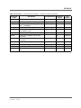
Configuration Options
Configuration Options
CPU
• MPC5200B, 384 MHz
Memory
• System RAM
- 32 MB, 64 MB, 128 MB or 256 MB
• NAND Flash
- 0 MB up to maximum available
• Boot Flash
- 2 MB, 4 MB or 8 MB
• Additional SDRAM
- 0 MB or 16 MB
• SRAM
- 0 MB or 2 MB
• 128 KB non-volatile FRAM instead of SRAM
I/O
• Up to 8 additional I/O functions through SA-Adapters™
- Mostly implemented in on-board FPGA
- RS232, RS422/485, binary I/O, keyboard/mouse, CAN...
- One-piece 3U front panels for different SA-Adapter™ combinations
• Front connections
- D-Sub connectors for Ethernet and COM/USB
• Second Ethernet channel at front through FPGA
Busless
• Also available as busless version (with external 5V supply)
Please note that some of these options may only be available for large volumes.
Please ask our sales staff for more information.
For available standard configurations see online data sheet.
MEN Mikro Elektronik GmbH
20F012N00 E3 – 2008-07-28
7
FPGA
FPGA
FPGA Capabilities
• FPGA Altera® Cyclone™ II EP2C20
- 18,752 logic elements
- 239,616 total RAM bits
• Connection
- Available pin count: 47 pins
- Functions available e.g. via I/O connector
Flexible Configuration
• This MEN board offers the possibility to add customized I/O functionality in
FPGA.
• It depends on the board type, pin counts and number of logic elements which IP
cores make sense and/or can be implemented. Please contact MEN for information on feasibility.
• Depending on the hardware platform, SA-Adapters™ can be used to realize the
physical lines.
MEN IP Cores
• MEN has a large number of standard IP cores to choose from.
• Examples:
- IDE (e.g. PIO mode 0, UDMA mode 5)
- UARTs
- CAN bus
- Display control
- Fast Ethernet (10/100Base-T)
- ...
• For IP cores developed by MEN please refer to our IP core overview.
- IP Core compare chart (PDF)
• MEN also offers development of new (customized) IP cores.
Third-Party IP Cores
• Third-party IP cores can also be used in combination with MEN IP cores.
• Examples:
- www.altera.com
- www.opencores.org
FPGA Design Environment
• Altera® offers free download of Quartus® II Web Edition
- Complete environment for FPGA and CPLD design
- Includes schematic- and text-based design entry
- Integrated VHDL and Verilog HDL synthesis and support for third-party synthesis software
- SOPC Builder system generation software
- Place-and-route, verification, and programming
» Altera® Quartus® II Web Edition FPGA design tool
MEN Mikro Elektronik GmbH
20F012N00 E3 – 2008-07-28
8
Product Safety
Product Safety
!
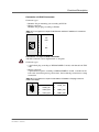
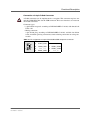
Electrostatic Discharge (ESD)
Computer boards and components contain electrostatic sensitive devices.
Electrostatic discharge (ESD) can damage components. To protect the board and
other components against damage from static electricity, you should follow some
precautions whenever you work on your computer.
• Power down and unplug your computer system when working on the inside.
• Hold components by the edges and try not to touch the IC chips, leads, or circuitry.
• Use a grounded wrist strap before handling computer components.
• Place components on a grounded antistatic pad or on the bag that came with the
component whenever the components are separated from the system.
• Store the board only in its original ESD-protected packaging. Retain the original
packaging in case you need to return the board to MEN for repair.
MEN Mikro Elektronik GmbH
20F012N00 E3 – 2008-07-28
9
About this Document
About this Document
This user manual describes the hardware functions of the board, connection of
peripheral devices and integration into a system. It also provides additional
information for special applications and configurations of the board.
The manual does not include detailed information on individual components (data
sheets etc.). A list of literature is given in the appendix.
History
Edition
Comments
Technical Content
Date of Issue
E1
First edition
H. Schubert, T. Wickleder, 2007-07-10
U. Franke, M. Beer
E2
Update for MENMON revi- H. Schubert, T. Wickleder, 2008-01-21
sion 1.13 with USB support U. Franke, M. Beer
E3
Description of board-toboard connector removed
(not relevant for user)
H. Schubert, T. Wickleder, 2008-07-28
U. Franke, M. Beer
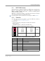
Conventions
!
italics
bold
monospace
hyperlink
This sign marks important notes or warnings concerning proper functionality of the
product described in this document. You should read them in any case.
Folder, file and function names are printed in italics.
Bold type is used for emphasis.
A monospaced font type is used for hexadecimal numbers, listings, C function
descriptions or wherever appropriate. Hexadecimal numbers are preceded by "0x".
Hyperlinks are printed in blue color.
The globe will show you where hyperlinks lead directly to the Internet, so you can
look for the latest information online.
IRQ#
/IRQ
Signal names followed by "#" or preceded by a slash ("/") indicate that this signal is
either active low or that it becomes active at a falling edge.
in/out
Signal directions in signal mnemonics tables generally refer to the corresponding
board or component, "in" meaning "to the board or component", "out" meaning
"coming from it".
Vertical lines on the outer margin signal technical changes to the previous edition of
the document.
MEN Mikro Elektronik GmbH
20F012N00 E3 – 2008-07-28
10
About this Document
Legal Information
MEN Mikro Elektronik reserves the right to make changes without further notice to any products herein. MEN makes no
warranty, representation or guarantee regarding the suitability of its products for any particular purpose, nor does MEN assume
any liability arising out of the application or use of any product or circuit, and specifically disclaims any and all liability,
including without limitation consequential or incidental damages.
"Typical" parameters can and do vary in different applications. All operating parameters, including "Typicals" must be
validated for each customer application by customer's technical experts.
MEN does not convey any license under its patent rights nor the rights of others.
Unless agreed otherwise, MEN products are not designed, intended, or authorized for use as components in systems intended
for surgical implant into the body, or other applications intended to support or sustain life, or for any other application in which
the failure of the MEN product could create a situation where personal injury or death may occur. Should Buyer purchase or
use MEN products for any such unintended or unauthorized application, Buyer shall indemnify and hold MEN and its officers,
employees, subsidiaries, affiliates, and distributors harmless against all claims, costs, damages, and expenses, and reasonable
attorney fees arising out of, directly or indirectly, any claim of personal injury or death associated with such unintended or
unauthorized use, even if such claim alleges that MEN was negligent regarding the design or manufacture of the part.
Unless agreed otherwise, the products of MEN Mikro Elektronik are not suited for use in nuclear reactors and for application
in medical appliances used for therapeutical purposes. Application of MEN products in such plants is only possible after the
user has precisely specified the operation environment and after MEN Mikro Elektronik has consequently adapted and
released the product.
ESM™, MDIS™, MDIS4™, MENMON™, M-Module™, M-Modules™, SA-Adapter™, SA-Adapters™, UBox™ and
USM™ are trademarks of MEN Mikro Elektronik GmbH. PC-MIP® is a registered trademark of MEN Micro, Inc. and SBS
Technologies, Inc. MEN Mikro Elektronik®, ESMexpress® and the MEN logo are registered trademarks of MEN Mikro
Elektronik GmbH.
Altera®, Avalon®, Cyclone™, Nios® and Quartus® are trademarks or registered trademarks of Altera Corp. Freescale™ and
PowerQUICC™ are trademarks of Freescale Semiconductor, Inc. PowerPC® is a registered trademark of IBM Corp.
CompactPCI® is a registered trademark of PCI Industrial Computer Manufacturers Group. Microsoft® and Windows® are
registered trademarks of Microsoft Corp. Windows® Vista™ is a trademark of Microsoft Corp. OS-9®, OS-9000® and
SoftStax® are registered trademarks of RadiSys Microware Communications Software Division, Inc. FasTrak™ and Hawk™
are trademarks of RadiSys Microware Communications Software Division, Inc. RadiSys® is a registered trademark of
RadiSys Corporation. PXI™ is a trademark of National Instruments Corp. QNX® is a registered trademark of QNX Ltd.
Tornado® and VxWorks® are registered trademarks of Wind River Systems, Inc.
All other products or services mentioned in this publication are identified by the trademarks, service marks, or product names
as designated by the companies who market those products. The trademarks and registered trademarks are held by the
companies producing them. Inquiries concerning such trademarks should be made directly to those companies. All other brand
or product names are trademarks or registered trademarks of their respective holders.
Information in this document has been carefully checked and is believed to be accurate as of the date of publication; however,
no responsibility is assumed for inaccuracies. MEN Mikro Elektronik accepts no liability for consequential or incidental
damages arising from the use of its products and reserves the right to make changes on the products herein without notice to
improve reliability, function or design. MEN Mikro Elektronik does not assume any liability arising out of the application or
use of the products described in this document.
Copyright © 2008 MEN Mikro Elektronik GmbH. All rights reserved.
Please recycle
Germany
MEN Mikro Elektronik GmbH
Neuwieder Straße 5-7
90411 Nuremberg
Phone +49-911-99 33 5-0
Fax +49-911-99 33 5-901
E-mail [email protected]
www.men.de
MEN Mikro Elektronik GmbH
20F012N00 E3 – 2008-07-28
France
MEN Mikro Elektronik SA
18, rue René Cassin
ZA de la Châtelaine
74240 Gaillard
Phone +33 (0) 450-955-312
Fax +33 (0) 450-955-211
E-mail [email protected]
www.men-france.fr
USA
MEN Micro, Inc.
24 North Main Street
Ambler, PA 19002
Phone (215) 542-9575
Fax (215) 542-9577
E-mail [email protected]
www.menmicro.com
11
Contents
Contents
1 Getting Started . . . . . . . . . . . . . . . . . . . . . . . . . . . . . . . . . . . . . . . . . . . . . . . .
1.1 Maps of the Board . . . . . . . . . . . . . . . . . . . . . . . . . . . . . . . . . . . . . . . .
1.2 Configuring the Hardware . . . . . . . . . . . . . . . . . . . . . . . . . . . . . . . . . .
1.3 Integrating the Board into a System . . . . . . . . . . . . . . . . . . . . . . . . . .
1.4 Installing Operating System Software. . . . . . . . . . . . . . . . . . . . . . . . .
18
18
20
21
22
2 Functional Description . . . . . . . . . . . . . . . . . . . . . . . . . . . . . . . . . . . . . . . . . .
2.1 Power Supply. . . . . . . . . . . . . . . . . . . . . . . . . . . . . . . . . . . . . . . . . . . .
2.1.1
System Supervision. . . . . . . . . . . . . . . . . . . . . . . . . . . . . . . .
2.2 Clock Supply . . . . . . . . . . . . . . . . . . . . . . . . . . . . . . . . . . . . . . . . . . . .
2.3 Real-Time Clock . . . . . . . . . . . . . . . . . . . . . . . . . . . . . . . . . . . . . . . . .
2.4 PowerPC CPU . . . . . . . . . . . . . . . . . . . . . . . . . . . . . . . . . . . . . . . . . . .
2.4.1
General . . . . . . . . . . . . . . . . . . . . . . . . . . . . . . . . . . . . . . . . .
2.4.2
Thermal Considerations . . . . . . . . . . . . . . . . . . . . . . . . . . . .
2.5 Bus Structure . . . . . . . . . . . . . . . . . . . . . . . . . . . . . . . . . . . . . . . . . . . .
2.6 Memory . . . . . . . . . . . . . . . . . . . . . . . . . . . . . . . . . . . . . . . . . . . . . . . .
2.6.1
SDRAM System Memory . . . . . . . . . . . . . . . . . . . . . . . . . . .
2.6.2
Boot Flash . . . . . . . . . . . . . . . . . . . . . . . . . . . . . . . . . . . . . . .
2.6.3
NAND Flash . . . . . . . . . . . . . . . . . . . . . . . . . . . . . . . . . . . . .
2.6.4
SRAM/FRAM . . . . . . . . . . . . . . . . . . . . . . . . . . . . . . . . . . . .
2.6.5
Additional SDRAM . . . . . . . . . . . . . . . . . . . . . . . . . . . . . . .
2.6.6
EEPROM. . . . . . . . . . . . . . . . . . . . . . . . . . . . . . . . . . . . . . . .
2.7 IDE Interface . . . . . . . . . . . . . . . . . . . . . . . . . . . . . . . . . . . . . . . . . . . .
2.7.1
Connection . . . . . . . . . . . . . . . . . . . . . . . . . . . . . . . . . . . . . .
2.8 USB Interface . . . . . . . . . . . . . . . . . . . . . . . . . . . . . . . . . . . . . . . . . . .
2.9 Ethernet Interfaces. . . . . . . . . . . . . . . . . . . . . . . . . . . . . . . . . . . . . . . .
2.9.1
Connection . . . . . . . . . . . . . . . . . . . . . . . . . . . . . . . . . . . . . .
2.9.2
General . . . . . . . . . . . . . . . . . . . . . . . . . . . . . . . . . . . . . . . . .
2.9.3
10Base-T . . . . . . . . . . . . . . . . . . . . . . . . . . . . . . . . . . . . . . . .
2.9.4
100Base-T . . . . . . . . . . . . . . . . . . . . . . . . . . . . . . . . . . . . . . .
2.10 UART COM1 Interface . . . . . . . . . . . . . . . . . . . . . . . . . . . . . . . . . . . .
2.11 UART COM10 Interface . . . . . . . . . . . . . . . . . . . . . . . . . . . . . . . . . . .
2.11.1 Connection . . . . . . . . . . . . . . . . . . . . . . . . . . . . . . . . . . . . . .
2.12 CAN Bus Interfaces. . . . . . . . . . . . . . . . . . . . . . . . . . . . . . . . . . . . . . .
2.12.1 Connection . . . . . . . . . . . . . . . . . . . . . . . . . . . . . . . . . . . . . .
2.12.2 General . . . . . . . . . . . . . . . . . . . . . . . . . . . . . . . . . . . . . . . . .
2.12.3 Basic CAN, Full CAN and Extended CAN . . . . . . . . . . . . .
2.13 GPIO . . . . . . . . . . . . . . . . . . . . . . . . . . . . . . . . . . . . . . . . . . . . . . . . . .
2.13.1 Connection . . . . . . . . . . . . . . . . . . . . . . . . . . . . . . . . . . . . . .
2.14 Reset Button and User LEDs. . . . . . . . . . . . . . . . . . . . . . . . . . . . . . . .
2.15 CompactPCI Interface . . . . . . . . . . . . . . . . . . . . . . . . . . . . . . . . . . . . .
2.15.1 General . . . . . . . . . . . . . . . . . . . . . . . . . . . . . . . . . . . . . . . . .
2.15.2 CompactPCI Extensions . . . . . . . . . . . . . . . . . . . . . . . . . . . .
23
23
23
23
24
24
24
24
24
25
25
25
25
25
25
25
26
26
28
30
30
32
32
32
33
35
35
38
38
45
45
46
48
50
51
51
51
MEN Mikro Elektronik GmbH
20F012N00 E3 – 2008-07-28
12
Contents
3 FPGA . . . . . . . . . . . . . . . . . . . . . . . . . . . . . . . . . . . . . . . . . . . . . . . . . . . . . . . .
3.1 General . . . . . . . . . . . . . . . . . . . . . . . . . . . . . . . . . . . . . . . . . . . . . . . .
3.2 Standard Factory FPGA Configuration . . . . . . . . . . . . . . . . . . . . . . . .
3.2.1
IP Cores. . . . . . . . . . . . . . . . . . . . . . . . . . . . . . . . . . . . . . . . .
3.2.2
FPGA Configuration Table . . . . . . . . . . . . . . . . . . . . . . . . . .
52
52
53
53
53
4 MENMON . . . . . . . . . . . . . . . . . . . . . . . . . . . . . . . . . . . . . . . . . . . . . . . . . . . .
4.1 General . . . . . . . . . . . . . . . . . . . . . . . . . . . . . . . . . . . . . . . . . . . . . . . .
4.1.1
State Diagram . . . . . . . . . . . . . . . . . . . . . . . . . . . . . . . . . . . .
4.2 Interacting with MENMON . . . . . . . . . . . . . . . . . . . . . . . . . . . . . . . .
4.2.1
Entering the Setup Menu/Command Line . . . . . . . . . . . . . .
4.3 Configuring MENMON for Automatic Boot . . . . . . . . . . . . . . . . . . .
4.4 Updating Boot Flash and NAND Flash . . . . . . . . . . . . . . . . . . . . . . . .
4.4.1
Update via the Serial Console using SERDL . . . . . . . . . . . .
4.4.2
Update from Network using NDL. . . . . . . . . . . . . . . . . . . . .
4.4.3
Update via Program Update Menu . . . . . . . . . . . . . . . . . . . .
4.4.4
Automatic Update Check . . . . . . . . . . . . . . . . . . . . . . . . . . .
4.4.5
Updating MENMON Code . . . . . . . . . . . . . . . . . . . . . . . . . .
4.5 Diagnostic Tests. . . . . . . . . . . . . . . . . . . . . . . . . . . . . . . . . . . . . . . . . .
4.5.1
Ethernet . . . . . . . . . . . . . . . . . . . . . . . . . . . . . . . . . . . . . . . . .
4.5.2
SDRAM . . . . . . . . . . . . . . . . . . . . . . . . . . . . . . . . . . . . . . . .
4.5.3
EEPROM. . . . . . . . . . . . . . . . . . . . . . . . . . . . . . . . . . . . . . . .
4.5.4
IDE/NAND Flash . . . . . . . . . . . . . . . . . . . . . . . . . . . . . . . . .
4.5.5
COM1 Port . . . . . . . . . . . . . . . . . . . . . . . . . . . . . . . . . . . . . .
4.5.6
Primary/Secondary MENMON. . . . . . . . . . . . . . . . . . . . . . .
4.5.7
Watchdog Timer Test . . . . . . . . . . . . . . . . . . . . . . . . . . . . . .
4.5.8
RTC . . . . . . . . . . . . . . . . . . . . . . . . . . . . . . . . . . . . . . . . . . . .
4.6 MENMON Configuration and Organization . . . . . . . . . . . . . . . . . . . .
4.6.1
Consoles . . . . . . . . . . . . . . . . . . . . . . . . . . . . . . . . . . . . . . . .
4.6.2
Video Modes . . . . . . . . . . . . . . . . . . . . . . . . . . . . . . . . . . . . .
4.6.3
Abort Pin . . . . . . . . . . . . . . . . . . . . . . . . . . . . . . . . . . . . . . . .
4.6.4
MENMON Memory Map . . . . . . . . . . . . . . . . . . . . . . . . . . .
4.6.5
MENMON BIOS Logical Units . . . . . . . . . . . . . . . . . . . . . .
4.6.6
System Parameters . . . . . . . . . . . . . . . . . . . . . . . . . . . . . . . .
4.7 MENMON Commands . . . . . . . . . . . . . . . . . . . . . . . . . . . . . . . . . . . .
4.7.1
USB Commands . . . . . . . . . . . . . . . . . . . . . . . . . . . . . . . . . .
54
54
55
57
57
57
58
58
58
58
59
60
61
61
62
63
63
64
64
64
65
66
66
66
66
67
68
69
75
77
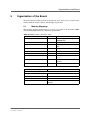
5 Organization of the Board . . . . . . . . . . . . . . . . . . . . . . . . . . . . . . . . . . . . . . .
5.1 Memory Mappings . . . . . . . . . . . . . . . . . . . . . . . . . . . . . . . . . . . . . . .
5.2 Interrupt Handling . . . . . . . . . . . . . . . . . . . . . . . . . . . . . . . . . . . . . . . .
5.3 SMB Devices . . . . . . . . . . . . . . . . . . . . . . . . . . . . . . . . . . . . . . . . . . . .
5.4 PCI Devices on Bus 0 . . . . . . . . . . . . . . . . . . . . . . . . . . . . . . . . . . . . .
79
79
80
81
81
MEN Mikro Elektronik GmbH
20F012N00 E3 – 2008-07-28
13
Contents
6 Appendix . . . . . . . . . . . . . . . . . . . . . . . . . . . . . . . . . . . . . . . . . . . . . . . . . . . . . 82
6.1 Literature and Web Resources . . . . . . . . . . . . . . . . . . . . . . . . . . . . . . . 82
6.1.1
PowerPC . . . . . . . . . . . . . . . . . . . . . . . . . . . . . . . . . . . . . . . . 82
6.1.2
PCI-104 . . . . . . . . . . . . . . . . . . . . . . . . . . . . . . . . . . . . . . . . . 82
6.1.3
Ethernet . . . . . . . . . . . . . . . . . . . . . . . . . . . . . . . . . . . . . . . . . 82
6.1.4
IDE . . . . . . . . . . . . . . . . . . . . . . . . . . . . . . . . . . . . . . . . . . . . 82
6.1.5
CAN Bus . . . . . . . . . . . . . . . . . . . . . . . . . . . . . . . . . . . . . . . . 83
6.1.6
USB . . . . . . . . . . . . . . . . . . . . . . . . . . . . . . . . . . . . . . . . . . . . 83
6.2 Finding out the Board’s Article Number, Revision and Serial Number83
MEN Mikro Elektronik GmbH
20F012N00 E3 – 2008-07-28
14
Figures
Figure 1.
Figure 2.
Figure 3.
Figure 4.
Figure 5.
Figure 6.
Figure 7.
Map of the board – front view . . . . . . . . . . . . . . . . . . . . . . . . . . . . . . .
Map of the board – top view. . . . . . . . . . . . . . . . . . . . . . . . . . . . . . . . .
Position of Fuse for CAN Bus Protection on Plug-on Board . . . . . . . .
FPGA – Block diagram (exemplary) . . . . . . . . . . . . . . . . . . . . . . . . . .
MENMON – State diagram, Degraded Mode/Full Mode . . . . . . . . . .
MENMON – State diagram, Main State . . . . . . . . . . . . . . . . . . . . . . .
Label giving the board’s article number, revision and serial number
(complete product) . . . . . . . . . . . . . . . . . . . . . . . . . . . . . . . . . . . . . . . .
Figure 8. Labels giving the board’s article number, revision and serial number
(plug-on CPU board) . . . . . . . . . . . . . . . . . . . . . . . . . . . . . . . . . . . . . .
MEN Mikro Elektronik GmbH
20F012N00 E3 – 2008-07-28
18
19
39
52
55
56
83
83
15
Tables
Table 1.
Table 2.
Table 3.
Table 4.
Table 5.
Table 6.
Table 7.
Table 8.
Table 9.
Table 10.
Table 11.
Table 12.
Table 13.
Table 14.
Table 15.
Table 16.
Table 17.
Table 18.
Table 19.
Table 20.
Table 21.
Table 22.
Table 23.
Table 24.
Table 25.
Table 26.
Table 27.
Table 28.
Table 29.
Table 30.
Table 31.
Table 32.
Table 33.
Table 34.
Table 35.
Table 36.
Table 37.
Table 38.
Table 39.
Table 40.
MEN Mikro Elektronik GmbH
20F012N00 E3 – 2008-07-28
Pin assignment of 44-pin IDE plug connector . . . . . . . . . . . . . . . . . . . 27
Signal mnemonics of 44-pin IDE plug connector . . . . . . . . . . . . . . . . 27
Signal mnemonics of USB interface . . . . . . . . . . . . . . . . . . . . . . . . . . 28
Pin assignment of USB Series A connector . . . . . . . . . . . . . . . . . . . . . 28
Pin assignment of 9-pin D-Sub USB/COM1 receptacle connector . . . 29
Signal mnemonics of Ethernet 10Base-T/100Base-TX interface. . . . . 30
Pin assignment of 8-pin RJ45 Ethernet 10Base-T/100Base-T connectors
(LAN1..2) . . . . . . . . . . . . . . . . . . . . . . . . . . . . . . . . . . . . . . . . . . . . . . . 31
Pin assignment of 9-pin D-Sub 10Base-T/100Base-TX plug connector
(LAN1 and LAN2) . . . . . . . . . . . . . . . . . . . . . . . . . . . . . . . . . . . . . . . . 31
Signal mnemonics of UART COM1 interface . . . . . . . . . . . . . . . . . . . 33
Pin assignment of 8-pin RJ45 UART connector (COM1) . . . . . . . . . . 33
Pin assignment of 9-pin D-Sub COM1/USB receptacle connector . . . 34
Pin assignment of 40-pin I/O plug connector – COM10 . . . . . . . . . . . 35
Signal mnemonics of 40-pin I/O plug connector – COM10 . . . . . . . . 35
Pin assignment of 10-pin CAN bus plug connector (CAN1) . . . . . . . . 38
Pin assignment of 10-pin CAN bus plug connector (CAN2) . . . . . . . . 38
Signal mnemonics of CAN bus interfaces . . . . . . . . . . . . . . . . . . . . . . 38
CAN bus transfer rates related to line lengths and cables . . . . . . . . . . 45
Assignment of 16Z034_GPIO controllers . . . . . . . . . . . . . . . . . . . . . . 46
Signal mnemonics of 40-pin and 26-pin GPIO connectors . . . . . . . . . 47
Pin assignment of 40-pin GPIO connector – GPIO0.x/1.x/2.x . . . . . . 48
Pin assignment of 26-pin GPIO connector – GPIO2.x/3.x/4.x . . . . . . 49
Front-panel LEDs . . . . . . . . . . . . . . . . . . . . . . . . . . . . . . . . . . . . . . . . . 50
Pin assignment of CompactPCI J2 (110-pin type "B" modified) . . . . . 51
Signal mnemonics of CompactPCI J2 . . . . . . . . . . . . . . . . . . . . . . . . . 51
FPGA – Factory standard configuration table for F12N . . . . . . . . . . . 53
MENMON – Program update files and locations . . . . . . . . . . . . . . . . 58
MENMON – Diagnostic tests: Ethernet. . . . . . . . . . . . . . . . . . . . . . . . 61
MENMON – Diagnostic tests: SDRAM . . . . . . . . . . . . . . . . . . . . . . . 62
MENMON – Diagnostic tests: EEPROM . . . . . . . . . . . . . . . . . . . . . . 63
MENMON – Diagnostic tests: IDE/NAND Flash . . . . . . . . . . . . . . . . 63
MENMON – Diagnostic tests: COM1 port . . . . . . . . . . . . . . . . . . . . . 64
MENMON – Diagnostic tests: Primary/Secondary MENMON . . . . . 64
MENMON – Diagnostic tests: Watchdog timer. . . . . . . . . . . . . . . . . . 64
MENMON – Diagnostic tests: RTC. . . . . . . . . . . . . . . . . . . . . . . . . . . 65
MENMON – System parameters for console selection . . . . . . . . . . . . 66
MENMON – Address map (full-featured mode) . . . . . . . . . . . . . . . . . 67
MENMON – Boot Flash memory map (2 MB) . . . . . . . . . . . . . . . . . . 67
MENMON – Controller Logical Units (CLUNs). . . . . . . . . . . . . . . . . 68
MENMON – Device Logical Units (DLUNs) . . . . . . . . . . . . . . . . . . . 68
MENMON – F12N system parameters – autodetected parameters . . . 69
16
Table 41. MENMON – F12N system parameters – production data . . . . . . . . . .
Table 42. MENMON – F12N system parameters – persistent parameters . . . . .
Table 43. MENMON – F12N system parameters – VxWorks bootline
parameters. . . . . . . . . . . . . . . . . . . . . . . . . . . . . . . . . . . . . . . . . . . . . . .
Table 44. MENMON – Reset causes through system parameter rststat. . . . . . . .
Table 45. MENMON – Voltage limits through system parameter psrXXX . . . .
Table 46. MENMON – Watchdog timeout through system parameter wdt. . . . .
Table 47. MENMON – Command Reference . . . . . . . . . . . . . . . . . . . . . . . . . . .
Table 48. Memory map – processor view . . . . . . . . . . . . . . . . . . . . . . . . . . . . . .
Table 49. Address mapping for PCI . . . . . . . . . . . . . . . . . . . . . . . . . . . . . . . . . . .
Table 50. BATS set up by MENMON . . . . . . . . . . . . . . . . . . . . . . . . . . . . . . . . .
Table 51. MENMON interrupt numbering. . . . . . . . . . . . . . . . . . . . . . . . . . . . . .
Table 52. SMB devices on bus 0 . . . . . . . . . . . . . . . . . . . . . . . . . . . . . . . . . . . . .
Table 53. SMB devices on bus 1 . . . . . . . . . . . . . . . . . . . . . . . . . . . . . . . . . . . . .
Table 54. PCI devices on bus 0 . . . . . . . . . . . . . . . . . . . . . . . . . . . . . . . . . . . . . .
MEN Mikro Elektronik GmbH
20F012N00 E3 – 2008-07-28
70
70
72
73
73
74
75
79
79
80
80
81
81
81
17
Getting Started
1
Getting Started
This chapter gives an overview of the board and some hints for first installation in a
system.
The F12N uses a plug-on module for CPU and I/O functionality. This plug-on board
also incorporates the two CAN bus interfaces.
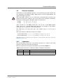
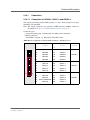
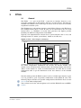
1.1
Maps of the Board
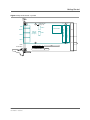
Figure 1. Map of the board – front view
Additional
F12N Standard SA-Adapters
(optional)
USB
CAN1
COM1
LAN2
CAN2
LAN1
1 2 3 4
RESET
MEN Mikro Elektronik GmbH
20F012N00 E3 – 2008-07-28
COM10
18
Getting Started
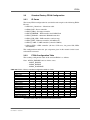
Figure 2. Map of the board – top view
CAN bus fuse
(facing out)
A1
A1
CAN 2
EM1N J2 – I/O
MPC5200B
COM1
Plug-on
Module
LAN2
CAN 1
(facing in)
EM1N J1 – PCI-104
USB
J2
LAN1
J1
LEDs
Reset button
GPIO0.x/1.x/2.x
MEN Mikro Elektronik GmbH
20F012N00 E3 – 2008-07-28
IDE
GPIO2.x/3.x/4.x
COM10
19
Getting Started
1.2
Configuring the Hardware
You should check your hardware requirements before installing the board in a
system, since most modifications are difficult or even impossible to do when the
board is mounted in a rack.
The following check list gives an overview on what you might want to configure.
; UART (COM10) and CAN bus extension through MEN standard SA-Adapters
The board provides
- one 40-pin I/O connector for connection of an additional COM interface (COM10) and
- two 10-pin connectors on the plug-on board for connection of two CAN
bus interfaces.
MEN provides a range of standard adapters (different interfaces for COM10
and a CAN standard adapter) and a mounting kit for three 9-pin D-Sub connectors accessible through a second front panel.
Please see MEN’s website for ordering information.
Refer to Chapter 2.11.1.1 Installing an SA-Adapter for COM10 on page
36 and Chapter 2.12.1.2 Installing SA-Adapters for CAN Bus on page 40
for SA-Adapter connection.
; IDE devices
The board provides an IDE connector for hard disks or other IDE devices.
MEN also offers a suitable adapter cable for two devices.
Please see MEN’s website for ordering information.
Refer to Chapter 2.7 IDE Interface on page 26 for details on the IDE
interface.
MEN Mikro Elektronik GmbH
20F012N00 E3 – 2008-07-28
20
Getting Started
1.3
Integrating the Board into a System
You can use the following check list when installing the board in a system for the
first time and with minimum configuration.
!
The board is completely trimmed on delivery.
; Power-down the system.
; Remove all boards from the CompactPCI system.
; Insert the F12N into the system slot of your CompactPCI system, making sure
that the CompactPCI connectors are properly aligned.
Note: The system slot of every CompactPCI system is marked by a
triangle
on the backplane and/or at the front panel. It also has red guide rails.
; Connect a terminal to the RS232 interface COM1 (RJ45 connector).
(MEN offers an adapter cable with a standard 9-pin D-Sub plug connector.
Please see MEN’s website for ordering information.)
; Set your terminal to the following protocol:
-
9600 baud data transmission rate
8 data bits
1 stop bit
No parity
; Power-up the system.
; The terminal displays a message similar to the following:
___________________ Secondary MENMON for MEN EM01 01.13 _____________________
|
|
|
(c) 2005 - 2007 MEN Mikro Elektronik GmbH Nuremberg
|
|
MENMON 2nd Edition, Created Dec 14 2007
16:02:43
|
|_____________________________________________________________________________|
|
CPU Board: EM01-00
|
CPU: MPC5200 Rev. B2
|
| Serial Number: 88
|
CPU/MEM Clk: 384 / 128 MHz
|
|
HW Revision: 01.11.02
|XLB/IPB/PCI Clk: 128 / 64 / 32 MHz
|
|
DDR SDRAM: 128 MB
|
Watchdog CFG: non-safety mode
|
|Production date: 12/19/2005
|
Reset Cause: by software
|
|
Last repair:
|
SRAM/FLASH: 2048 kB /
2 MB
|
|_____________________________________________________________________________|
| Carrier Board:
|
\___________________________________________________________________________/
Setting speed of NETIF 0 to AUTO
press 'ESC' for MENMON, 's' for setup
Test SDRAM
: OK
Test ETHER0
: OK
Test EEPROM
: OK
Test RTC
: OK
Test IDE0-NAND
: OK
Test TOUCH
: OK
NOW AUTOEXECUTING: BO
No default start address configured. Stop.
Setup network interface CLUN 0x02, 00:c0:3a:40:00:07 AUTO
Telnet daemon started on port 23
HTTP daemon started on port 80
MenMon>
MEN Mikro Elektronik GmbH
20F012N00 E3 – 2008-07-28
21
Getting Started
; Now you can use the MENMON BIOS/firmware (see detailed description in
Chapter 4 MENMON on page 54).
; Observe the installation instructions for the respective software.
1.4
Installing Operating System Software
The board supports Linux (ELinOS), VxWorks and QNX.
!
By standard, no operating system is installed on the board. Please refer to the
operating system installation documentation on how to install the software!
You can find any software available on MEN’s website.
MEN Mikro Elektronik GmbH
20F012N00 E3 – 2008-07-28
22
Functional Description
2
Functional Description
The following describes the individual functions of the board and their
configuration on the board. There is no detailed description of the individual
controller chips and the CPU. They can be obtained from the data sheets or data
books of the semiconductor manufacturer concerned (Chapter 6.1 Literature and
Web Resources on page 82).
2.1
Power Supply
The board is supplied with +5V and +3.3V via the CompactPCI bus. The plug-on
CPU card itself is supplied via PCI-104 connectors J1/J2.
The on-board power supply generates the 1.5V core voltage for the CPU, 2.5V for
memory and the 1.2V core voltage for the FPGA.
On F12N a voltage regulator can be assembled as an option which generates +3.3V
for the plug-on module and PCI bridge. In this case the board can be operated as a
stand-alone system with a single +5V supply.
2.1.1
System Supervision
The F12N provides a reset CPLD which generates the reset signal to the CPU. It
contains a watchdog that must be triggered by software. The reason of the last reset
can be read by software from this CPLD.
A voltage monitor device including a thermometer is connected to this reset CPLD.
Whenever one of the required supply voltages is running out of the allowed range,
the monitor puts the CPU into reset.
The current voltage and temperature values can be read out by software via I²C bus. The
temperature accuracy is ±2°C (max.) @ -25°C..100°C and ±3°C (max.) @ -55°C..125°C.
See also Chapter 4.6.6.3 Hardware Monitor Support – Parameter psrXXX on page
73, Chapter 4.6.6.4 Watchdog – Parameter wdt on page 74.
2.2
Clock Supply
A 32-MHz oscillator is used as the main clock source. This clock is fed into the
CPU and is internally multiplied to a 64-MHz SDRAM clock and XLB_CLK. The
XLB_CLK is multiplied by another PLL to the 384-MHz core frequency.
The PCI and local bus interfaces operate at 32MHz. The clock for the primary PCI
bus is supplied from the CPU and driven via PLL to the FPGA and PCI-to-PCI
bridge.
Clocks for the CompactPCI bus are driven by the PCI-to-PCI bridge and are derived
from the primary PCI bus clock.
Two further oscillators provide the 48-MHz USB clock and 25-MHz Ethernet clock.
MEN Mikro Elektronik GmbH
20F012N00 E3 – 2008-07-28
23
Functional Description
2.3
Real-Time Clock
The board includes a real-time clock of type EPSON RTC-8581. Interrupt
generation of the RTC is not supported. For data retention during power off the RTC
is backed up by a GoldCap capacitor. The GoldCap gives an autonomy of approx.
15 hours when fully loaded. Under normal conditions, replacement should be
superfluous during lifetime of the board.
A control flag indicates a back-up power fail condition. In this case the contents of
the RTC cannot be expected to be valid.
2.4
PowerPC CPU
2.4.1
General
The MPC5200B is based on a 400-MHz MPC603e PowerPC core with an
integrated double precision Floating Point Unit (FPU) that is qualified at -40°C to
+85°C. It incorporates a hardware-based memory management unit (MMU) for
advanced memory protection schemes, fast task switching and broad RTOS support.
The MPC5200B was designed for fast data throughput and processing. The
integrated BestComm DMA controller offloads the main MPC603e core from I/O
intensive data transfers. An integrated Double Data Rate (DDR) memory controller
accelerates data access with an effective memory bus speed of 266 MHz. A PCI
interface backed by the BestComm DMA controller and DDR memory support
enables high-speed data transfers in and out of the MPC5200B.
2.4.2
Thermal Considerations
The CPU operates on extremely low power. It consumes around 1 W of power only.
The F12N can be operated in the industrial temperature range without a heat sink if
enough airflow over the board is provided. MEN recommends to provide an
airspeed of 2 m/s over the CPU which equals about 10 m³/h airflow through a
CompactPCI slot.
If this cannot be established due to the assembly situation MEN recommends to use
a suitable heat sink.
2.5
Bus Structure
The MPC5200B provides a multifunction external bus which is 32 bits wide and
operates at 32 MHz.
The boot Flash and SRAM/FRAM are hooked up to this bus.
This bus can also act as a Rev. 2.2 PCI interface. It is connected to the on-board
FPGA and via J1 to the PCI-to-CompactPCI bridge.
The F12N always operates as the system slot controller on the CompactPCI bus. It
supports up to 7 external masters on the CompactPCI bus.
MEN Mikro Elektronik GmbH
20F012N00 E3 – 2008-07-28
24
Functional Description
2.6
Memory
2.6.1
SDRAM System Memory
The board provides up to 256 MB on-board, soldered DDR (double data rate)
SDRAM on two memory components. It is organized as four memory banks. The
memory bus is 32 bits wide and operates at 128 MHz (physical).
2.6.2
Boot Flash
The board has on-board Flash. It is controlled by the CPU and can accommodate
8 MB. The data bus is 8 bits wide.
Flash memory contains the boot software for the MENMON/operating system
bootstrapper and application software. The MENMON sectors are softwareprotected against illegal write transactions through a password in the serial
download function of MENMON (cf. Chapter 4.4 Updating Boot Flash and NAND
Flash on page 58). The boot Flash also contains the configuration data for the onboard FPGA.
2.6.3
NAND Flash
The board includes up to 1 GB soldered NAND Flash memory controlled by the
FPGA. The data bus is 8 bits wide.
MEN's NAND-ATA controller provides wear leveling without user interaction.
Using the NAND-ATA controller the NAND Flash is seen as an ATA disk.
NAND Flash provides 100,000 erase cycles minimum and 10 years data retention.
See also Chapter 4.4 Updating Boot Flash and NAND Flash on page 58.
2.6.4
SRAM/FRAM
The board can be supplied with 2 MB battery-backed SRAM memory connected to
the multifunction external bus.
For data retention during power off the SRAM is backed up by a GoldCap capacitor.
The GoldCap gives an autonomy of approx. 15 hours when fully loaded. Under
normal conditions, replacement should be superfluous during lifetime of the board.
Alternatively, 128 KB non-volatile FRAM are possible instead of SRAM. The
FRAM does not need a back-up voltage for data retention.
2.6.5
Additional SDRAM
The board can be supplied with 16 MB additional SDRAM. It is controlled by the
FPGA and a part of it is used for the NAND Flash firmware. It can also be used for
graphics, for instance.
2.6.6
EEPROM
The board has an 8-kbit serial EEPROM for factory data, MENMON parameters,
and for the VxWorks bootline.
MEN Mikro Elektronik GmbH
20F012N00 E3 – 2008-07-28
25
Functional Description
2.7
IDE Interface
The parallel IDE (PATA) interface handles the exchange of information between the
processor and peripheral devices such as hard disks, ATA CompactFlash cards and
CD-ROM drives.
The IDE interface is controlled by the FPGA and supports up to two ATA devices in
PIO mode 0. One device acts as a master, the other as a slave.
2.7.1
Connection
You can connect one or two devices to the standard 44-pin connector. MEN offers a
suitable adapter cable for two devices. For ordering options, please see MEN’s
website.
The 44-pin IDE connector is located at the top side of F12N. The pinning of the IDE
connector complies with the ATA-4/ATAPI specification.
Connector types:
• 44-pin, 2-row plug, 2mm pitch
• Mating connector:
44-pin, 2-row receptacle, 2mm pitch
MEN Mikro Elektronik GmbH
20F012N00 E3 – 2008-07-28
26
Functional Description
Table 1. Pin assignment of 44-pin IDE plug connector
1
43
2
44
1
IDE_RST#
2
GND
3
IDE_D[7]
4
IDE_D[8]
5
IDE_D[6]
6
IDE_D[9]
7
IDE_D[5]
8
IDE_D[10]
9
IDE_D[4]
10
IDE_D[11]
11
IDE_D[3]
12
IDE_D[12]
13
IDE_D[2]
14
IDE_D[13]
15
IDE_D[1]
16
IDE_D[14]
17
IDE_D[0]
18
IDE_D[15]
19
GND
20
-
21
-
22
GND
23
IDE_WR#
24
GND
25
IDE_RD#
26
GND
27
IDE_RDY
28
-
29
-
30
GND
31
IDE_IRQ
32
-
33
IDE_A[1]
34
GND
35
IDE_A[0]
36
IDE_A[2]
37
IDE_CS1#
38
IDE_CS3#
39
-
40
GND
41
+5V
42
+5V
43
GND
44
GND
Table 2. Signal mnemonics of 44-pin IDE plug connector
Signal
Function
+5V
out
+5V power supply, current-limited by a fuse
GND
-
Digital ground
IDE_A[2:0]
out
IDE address [2:0]
IDE_CS1#
out
IDE chip select 1
IDE_CS3
out
IDE chip select 3
IDE_D[15:0]
in/out
IDE data [15:0]
IDE_IRQ
in
IDE interrupt request
IDE_RD#
out
IDE read strobe
IDE_RDY
in
IDE ready
IDE_RST#
out
IDE reset
IDE_WR#
out
IDE write strobe
MEN Mikro Elektronik GmbH
20F012N00 E3 – 2008-07-28
Direction
27
Functional Description
2.8
USB Interface
The board provides one USB 1.1 port with a data rate of up to 12 Mbits/s, which is
routed to a front-panel connector. You can connect a USB peripheral device directly
to the F12N without an external hub. To attach multiple devices, connect an external
hub to the USB port of the board (often monitors or keyboards provide USB hub
functionality).
The USB connector can source up to 1.0A/5V.
Table 3. Signal mnemonics of USB interface
Signal
Direction
Function
+5V
out
+5V power supply
GND
-
Digital ground
USB_D-, USB_D+
in/out
USB port lines, differential pair
Connection via USB Series A Connector
Connector types:
• 4-pin USB Series A receptacle according to Universal Serial Bus Specification
Revision 1.1
• Mating connector:
4-pin USB Series A plug according to Universal Serial Bus Specification Revision 1.1
Table 4. Pin assignment of USB Series A connector
1
2
3
4
MEN Mikro Elektronik GmbH
20F012N00 E3 – 2008-07-28
1
+5V
2
USB_D-
3
USB_D+
4
GND
28
Functional Description
Connection via 9-pin D-Sub Connector
!
A D-Sub connector can be implemented as an option. This connector replaces not
only the USB connector but also the COM1 RJ45 connector. These two interfaces
are routed to one D-Sub connector.
Connector types:
• 9-pin D-Sub receptacle according to DIN41652/MIL-C-24308, with thread bolt
UNC 4-40
• Mating connector:
9-pin D-Sub plug according to DIN41652/MIL-C-24308, available for ribbon
cable (insulation piercing connection), hand-soldering connection or crimp connection
Table 5. Pin assignment of 9-pin D-Sub USB/COM1 receptacle connector
1
5
MEN Mikro Elektronik GmbH
20F012N00 E3 – 2008-07-28
6
9
1
USB_GND
2
COM1_RXD
6
USB_D-
3
COM1_TXD
7
COM1_RTS#
4
USB_+5V
8
COM1_CTS#
5
COM1_GND
9
USB_D+
29
Functional Description
2.9
Ethernet Interfaces
The F12N has two Fast Ethernet interfaces, one controlled by the CPU (LAN1) and
one controlled by the FPGA (LAN2). Both interfaces provide 10/100 Mbits/s and
support full-duplex operation.
!
The unique MAC addresses are set at the factory and should not be changed. Any
attempt to change these addresses may create node or bus contention and thereby
render the board inoperable. The MAC addresses on F12N are:
• LAN1:
• LAN2:
0x 00 C0 3A 40 xx xx
0x 00 C0 3A 41 xx xx
where "00 C0 3A" is the MEN vendor code, "40" and "41" are the MEN product
codes, and "xx xx" is the the F12N offset plus the serial number of the product,
which depends on your board, in hexadecimal form.
The F12N offset and valid offset plus serial number range is 0x8000 (up to
0xFFFF).
The serial number is added to the offset, for example:
• Serial number 0042: 0x xx xx = 0x8000 + 0x002A = 0x 80 2A
• Serial number 4097: 0x xx xx = 0x8000 + 0x1001 = 0x 90 01
(See also Chapter 6.2 Finding out the Board’s Article Number, Revision and Serial
Number on page 83.)
2.9.1
Connection
Two standard RJ45 connectors or one D-Sub connector are available at the front
panel for connection to network environments.
The pin assignments correspond to the Ethernet specification IEEE802.3.
Table 6. Signal mnemonics of Ethernet 10Base-T/100Base-TX interface
Signal
Function
RX+/-
in
Differential pair of receive data lines for 10/100Base-T
TX+/-
out
Differential pair of transmit data lines for 10/100Base-T
MEN Mikro Elektronik GmbH
20F012N00 E3 – 2008-07-28
Direction
30
Functional Description
Connection via RJ45 Connectors
Connector types:
• Modular 8/8-pin mounting jack according to FCC68
• Mating connector:
Modular 8/8-pin plug according to FCC68
Table 7. Pin assignment of 8-pin RJ45 Ethernet 10Base-T/100Base-T connectors
(LAN1..2)
1
8
1
TX+
2
TX-
3
RX+
4
-
5
-
6
RX-
7
-
8
-
Connection via 9-pin D-Sub Connector
!
A D-Sub connector can be implemented as an option.
Connector types:
• 9-pin D-Sub plug according to DIN41652/MIL-C-24308, with thread bolt UNC
4-40
• Mating connector:
9-pin D-Sub receptacle according to DIN41652/MIL-C-24308, available for ribbon cable (insulation piercing connection), hand-soldering connection or crimp
connection
Table 8. Pin assignment of 9-pin D-Sub 10Base-T/100Base-TX plug connector
(LAN1 and LAN2)
6
9
MEN Mikro Elektronik GmbH
20F012N00 E3 – 2008-07-28
1
5
1
LAN1_TX+
6
LAN1_TX-
2
LAN2_TX+
7
LAN2_TX-
3
-
8
LAN2_RX-
4
LAN2_RX+
9
LAN1_RX-
5
LAN1_RX+
31
Functional Description
2.9.2
General
Ethernet is a local-area network (LAN) protocol that uses a bus or star topology and
supports data transfer rates of 100Mbps and more. The Ethernet specification served
as the basis for the IEEE 802.3 standard, which specifies the physical and lower
software layers. Ethernet uses the CSMA/CD access method to handle simultaneous
demands. It is one of the most widely implemented LAN standards.
Ethernet networks provide high-speed data exchange in areas that require
economical connection to a local communication medium carrying bursty traffic at
high-peak data rates.
A classic Ethernet system consists of a backbone cable and connecting hardware
(e.g. transceivers), which links the controllers of the individual stations via
transceiver (transmitter-receiver) cables to this backbone cable and thus permits
communication between the stations.
2.9.3
10Base-T
10Base-T is one of several adaptations of the Ethernet (IEEE 802.3) standard for
Local Area Networks (LANs). The 10Base-T standard (also called Twisted Pair
Ethernet) uses a twisted-pair cable with maximum lengths of 100 meters. The cable
is thinner and more flexible than the coaxial cable used for the 10Base-2 or
10Base-5 standards. Since it is also cheaper, it is the preferable solution for costsensitive applications.
Cables in the 10Base-T system connect with RJ45 connectors. A star topology is
common with 12 or more computers connected directly to a hub or concentrator.
The 10Base-T system operates at 10Mbps and uses baseband transmission methods.
2.9.4
100Base-T
The 100Base-T networking standard supports data transfer rates up to 100Mbps.
100Base-T is actually based on the older Ethernet standard. Because it is 10 times
faster than Ethernet, it is often referred to as Fast Ethernet. Officially, the 100Base-T
standard is IEEE 802.3u.
Like Ethernet, 100Base-T is based on the CSMA/CD LAN access method. There
are several different cabling schemes that can be used with 100Base-T, e.g.
100Base-TX, with two pairs of high-quality twisted-pair wires.
MEN Mikro Elektronik GmbH
20F012N00 E3 – 2008-07-28
32
Functional Description
2.10
UART COM1 Interface
COM1 is a standard RS232 interface. It is available via an RJ45 or D-Sub connector
at the front panel. The serial interface is controlled by Programmable Serial
Controller PSC1 of the CPU.
Table 9. Signal mnemonics of UART COM1 interface
Signal
Direction
Function
CTS#
in
Clear to send
GND
-
Ground
RTS#
out
Request to send
RXD
in
Receive data
TXD
out
Transmit data
Connection via RJ45 Connector
Connector types:
• Modular 8/8-pin mounting jack according to FCC68
• Mating connector:
Modular 8/8-pin plug according to FCC68
Table 10. Pin assignment of 8-pin RJ45 UART connector (COM1)
1
1
-
2
-
3
-
4
GND
5
RXD
6
TXD
7
CTS#
8
RTS#
8
MEN Mikro Elektronik GmbH
20F012N00 E3 – 2008-07-28
33
Functional Description
Connection via 9-pin D-Sub Connector
!
A D-Sub connector can be implemented as an option. This connector replaces not
only the COM1 RJ45 but also the USB connector. These two interfaces are routed to
one D-Sub connector.
Connector types:
• 9-pin D-Sub receptacle according to DIN41652/MIL-C-24308, with thread bolt
UNC 4-40
• Mating connector:
9-pin D-Sub plug according to DIN41652/MIL-C-24308, available for ribbon
cable (insulation piercing connection), hand-soldering connection or crimp connection
Table 11. Pin assignment of 9-pin D-Sub COM1/USB receptacle connector
1
5
MEN Mikro Elektronik GmbH
20F012N00 E3 – 2008-07-28
6
9
1
USB_GND
2
COM1_RXD
6
USB_D-
3
COM1_TXD
7
COM1_RTS#
4
USB_+5V
8
COM1_CTS#
5
COM1_GND
9
USB_D+
34
Functional Description
2.11
UART COM10 Interface
The F12N provides an additional, LVTTL-level, UART interface controlled by the
FPGA on a 40-pin ribbon-cable connector. The UART port is compatible with
MEN’s SA-Adapter standard, which offers a selection of different physical
interfaces from RS232 to RS485.
MEN offers a mounting kit including a second front panel for three SA-Adapters
with 9-pin D-Sub connectors and suitable ribbon cables.
For ordering options and more information on SA-Adapters see MEN’s website.
2.11.1
Connection
Note: The 40-pin connector also includes a part of the GPIO lines, which are
described in Chapter 2.13 GPIO on page 46.
Connector types:
• 40-pin low-profile plug, 2.54mm pitch, for ribbon-cable connection
• Mating connector:
40-pin IDC receptacle, e.g. Elco Series 8290 IDC socket
Table 12. Pin assignment of 40-pin I/O plug connector – COM10
1
2
1
GND
2
+5V
3
TXD10
4
RXD10
5
DTR10#
6
RTS10#
7
DSR10#
8
CTS10#
9
DCD10#
10
RI10#
11
..
COM10
12
GPIO lines
39
..
GPIO lines
GPIO
40
Table 13. Signal mnemonics of 40-pin I/O plug connector – COM10
Signal
Function
+5V
-
+5V power supply, current-limited by a fuse
CTS#
in
Clear to send
DCD#
in
Data carrier detect
DSR#
in
Data set ready
DTR#
out
Data terminal ready
GND
-
Ground
RI#
in
Ring indicator
RTS#
out
Request to send
RXD
in
Receive data
TXD
out
Transmit data
MEN Mikro Elektronik GmbH
20F012N00 E3 – 2008-07-28
Direction
35
Functional Description
2.11.1.1 Installing an SA-Adapter for COM10
MEN offers a special mounting kit for easy installation of SA-Adapters. It includes
an additional front panel for three SA-Adapters and any ribbon cables needed.
Please refer to MEN’s website for ordering information.
!
Note: MEN gives no warranty on functionality and reliability of the board and SAAdapters used if you install SA-Adapters in a different way than described in
MEN’s documentation.
Perform the following steps to install standard SA-Adapters using MEN’s SAAdapter mounting kit:
; Power-down your system and remove the F12N from the system.
; Remove the COM10 blind connector from the additional front panel, if
installed: Loosen the two screws highlighted in the drawing.
USB
CAN1
COM1
LAN2
CAN2
LAN1
1 2 3 4
RESET
COM10
; Remove the two front panel screws and the two screws on top of the mounting
bolts of the SA-Adapter.
MEN Mikro Elektronik GmbH
20F012N00 E3 – 2008-07-28
36
Functional Description
; Plug the 40-pin prefolded ribbon cable to the 40-pin I/O connector on F12N.
; Plug the 10-pin connector of the ribbon cable to the 10-pin SA-Adapter connector.
; Use the front panel screws of the SA-Adapter to fasten the adapter at the additional front panel.
; You can now reinsert the board and the additional front panel into your system.
Make sure to fasten the SA-Adapter front panel appropriately in your enclosure!
MEN Mikro Elektronik GmbH
20F012N00 E3 – 2008-07-28
37
Functional Description
2.12
CAN Bus Interfaces
The F12N has two MSCAN interfaces inside the MPC5200B. The physical
interface is led to two 10-pin plug connectors. These connectors are compatible with
MEN’s SA-Adapters, so that you can easily lead them to standard D-Sub connectors
using ribbon cable.
For available SA-Adapters please see MEN’s website.
The interfaces support the 2.0 A/B CAN protocol. The data transfer rate is up to
1 Mbit/s.
2.12.1
Connection
The CAN bus connectors are located on the plug-on module’s top side, which faces
the carrier board. (See Figure 2, Map of the board – top view, on page 19.)
Connector types:
• 10-pin plug, IDC ribbon-cable connector according to DIN41651/MIL-C-83503,
plug connector with lock
• Mating connector:
10-pin receptacle, available with or without tension relief for ribbon-cable connection, 1.27mm pitch
Table 14. Pin assignment of 10-pin CAN bus plug connector (CAN1)1
10
9
2
1
10
GND
9
-
8
-
7
-
6
-
5
-
4
CAN_RXD1
3
CAN_TXD1
2
+5V
1
GND
Table 15. Pin assignment of 10-pin CAN bus plug connector (CAN2)2
10
9
2
1
10
GND
9
-
8
-
7
-
6
-
5
-
4
CAN_RXD2
3
CAN_TXD2
2
+5V
1
GND
Table 16. Signal mnemonics of CAN bus interfaces
Signal
Direction
Function
+5V
out
+5V power supply, protected by a fuse
GND
-
Digital ground
CAN_RXD
in
CAN bus data receive line
CAN_TXD
out
CAN bus data transmit line
1
CAN_TXD1 is controlled by CPU pin PSC2[0].
CAN_RXD1 is controlled by CPU pin PSC2[1].
2 CAN_TXD2 is controlled by CPU pin PSC2[2].
CAN_RXD2 is controlled by CPU pin PSC2[3].
MEN Mikro Elektronik GmbH
20F012N00 E3 – 2008-07-28
38
Functional Description
2.12.1.1 Fuse Protection
The CAN bus interfaces are protected by a fuse. This fuse is not intended to be
exchanged by the customer. Your warranty for the F12N will cease if you
exchange the fuse on your own. Please send your board to MEN for repair if a fuse
blows.
•
•
•
•
Current rating: 3A
Type: fast
Size: 1206
MEN part number: 5675-0003
The fuse is located on the plug-on board of F12N, on the board side facing out.
Figure 3. Position of Fuse for CAN Bus Protection on Plug-on Board
CAN bus fuse
(facing out)
A1
A1
CAN 2
EM1N J2 – I/O
MPC5200B
COM1
Plug-on
Module
LAN2
CAN 1
(facing in)
EM1N J1 – PCI-104
USB
J2
LAN1
J1
LEDs
t button
GPIO0.x/1.x/2.x
MEN Mikro Elektronik GmbH
20F012N00 E3 – 2008-07-28
IDE
GPIO2.x/3.x/4.x
COM10
39
Functional Description
2.12.1.2 Installing SA-Adapters for CAN Bus
MEN offers a special mounting kit for easy installation of SA-Adapters. It includes
an additional front panel for three SA-Adapters and any ribbon cables needed.
Please refer to MEN’s website for ordering information.
!
Note: MEN gives no warranty on functionality and reliability of the board and SAAdapters used if you install SA-Adapters in a different way than described in
MEN’s documentation.
Perform the following steps to install standard SA-Adapters using MEN’s SAAdapter mounting kit:
; Power-down your system and remove the F12N from the system.
; Remove the CAN1 or CAN2 blind connector from the additional front panel, if
installed: Loosen the two screws highlighted in the drawing.
(optional)
USB
CAN1
COM1
LAN2
CAN2
LAN1
1 2 3 4
RESET
MEN Mikro Elektronik GmbH
20F012N00 E3 – 2008-07-28
COM10
40
Functional Description
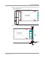
; Remove the plug-on module from the carrier board: Loosen and remove the
screws highlighted in red.
Take care not to lose the nuts of the plug-on module’s screws.
J2
Screws to uninstall
plug-on module from
carrier board
J1
; Remove the front panel: Loosen and remove the two screws highlighted in red.
Screws to uninstall
plug-on module from
carrier board
MEN Mikro Elektronik GmbH
20F012N00 E3 – 2008-07-28
Screws to
uninstall front
panel
41
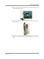
Functional Description
; Carefully remove the plug-on module from the carrier board by unplugging the
J1/J2 board-to-board connectors of the module and carrier, taking care not to
damage the two boards.
A1
CAN 2
MPC5200B
EM1N J2 – I/O
Plug-on
Module
A1
CAN 1
(facing in)
EM1N J1 – PCI-104
CAN bus fuse
(facing out)
J2
J1
IDE
GPIO2.x/3.x/4.x
GPIO0.x/1.x/2.x
COM10
; Remove the two front panel screws and the two screws on top of the mounting
bolts of the SA-Adapter.
MEN Mikro Elektronik GmbH
20F012N00 E3 – 2008-07-28
42
Functional Description
; Plug the suitable 10-pin prefolded ribbon cable to the respective 10-pin CAN
bus connector on F12N.
CAN1
CAN2
SA-Adapter
F12N
F12N
CAN2
CAN1
SA-Adapter
CAN1
CAN2
; Reinstall the plug-on module on the carrier card: Carefully align the J1/J2 connectors and press the plug-on module down until it sits tightly on the carrier
board.
; Reinstall the front panel: Place the front panel back over the connectors, taking
care not to damage the reset button and LEDs. Put back and fasten the two
screws removed before.
; Reinstall the four plug-on module installation screws at the bottom side of the
carrier board.
MEN Mikro Elektronik GmbH
20F012N00 E3 – 2008-07-28
43
Functional Description
; Plug the 10-pin connector of the ribbon cable to the 10-pin SA-Adapter connector.
(The photo shows only CAN1.)
; Use the front panel screws of the SA-Adapter to fasten the adapter at the additional front panel.
; You can now reinsert the board and the additional front panel into your system.
Make sure to fasten the SA-Adapter front panel appropriately in your enclosure!
MEN Mikro Elektronik GmbH
20F012N00 E3 – 2008-07-28
44
Functional Description
2.12.2
General
CAN bus provides an open fieldbus system for industrial applications.
Its primary characteristics are:
•
•
•
•
•
Bus length up to 1,000 m
Transfer rates: 62.5 kbits/s to 1 Mbits/s
High immunity to external and internal errors
Short message lengths (0..28 bytes)
Short transfer delays due to short messages
CAN allows multimaster access according to the CSMA/CA principle (Carrier
Sense Multiple Access with Collision Avoidance) with bitwise arbitration
depending on the message priority. If two or more network participants want to
access the bus simultaneously, it will always be the most important message that is
transmitted first. This avoids loss of transmission time.
The transfer rate depends on the line length:
Table 17. CAN bus transfer rates related to line lengths and cables
Transfer Rate
Line Length
Recommended Cables1
1 Mbit/s
40 m
0..40 m: 0.25 mm2, 0.34 mm2 AWG23, AWG22
500 kbits/s
100 m
40..300 m: 0.34 mm2..0.6 mm2 AWG22, AWG20
125 kbits/s
500 m
300..600 m: 0.5 mm2, 0.6 mm2 AWG20
62.5 kbits/s
1,000 m
600..1,000 m: 0.75 mm2, 0.8 mm2 AWG18
1
Length and cross section
At bit rates lower than 1 Mbits/s the bus length may be lengthened significantly. A
data rate of 62.5 kbits/s allows a bus length of 1,000 m. ISO 11898 compliant
transceivers specify max. bus length of about 1,000 m. However, it is allowed to use
bridge devices or repeaters to increase the allowed distance between ISO 11898
compliant nodes to more than 1,000 m.
2.12.3
Basic CAN, Full CAN and Extended CAN
CAN exists in two forms; a basic CAN and a higher form with an "acceptance
filter". Basic CAN has a tight coupling between the CPU and the CAN controller,
where all messages broadcast on the network have to be individually checked by the
microcontroller. This results in the CPU being "tied up" checking messages rather
than processing them, all of which tends to limit the practicable baud rate to
250kbaud. The introduction of an acceptance filter masks out the irrelevant
messages, using identifiers (ID) and presents the CPU with only those messages that
are of interest. This is usually referred to as Full CAN. The Full CAN protocol
allows for two lengths of identifiers: part A allows for 11 message identification
bits, which yield 2,032 different identifiers (16 are reserved), while Extended CAN
(part B) has 29 identification bits, producing 536,870,912 separate identifiers.
MEN Mikro Elektronik GmbH
20F012N00 E3 – 2008-07-28
45
Functional Description
2.13
GPIO
Five GPIO controllers are included in the FPGA. Each of them controls eight I/O
signals, totalling 40 signals. Four of these signals are fixed to specific functions:
GPIO2.4 is used as push-button reset input, and GPIO3.0, 3.1 and 3.5 are used to
control three of the front LEDs. This leaves 36 completely user-definable lines.
All pins are directly connected to the FPGA. Voltage levels are LVTTL.
You can control the GPIO lines through software using MDIS4 driver software
available on MEN’s website. The following table gives the assignment of the GPIO
controllers implemented in the F12N’s FPGA to their function on the board.
Normally you can identify the controllers by their instance numbers in your
operating system.
Table 18. Assignment of 16Z034_GPIO controllers
Instance
Function
0
GPIO lines 0.0 to 0.7 (bits 0..7)
1
GPIO lines 1.0 to 1.7 (bits 0..7)
2
GPIO lines 2.0 to 2.7 (bits 0..7)
GPIO2.4 is used for push button reset
3
GPIO lines 3.0 to 3.7 (bits 0..7)
GPIO3.0, GPIO3.1 and GPIO3.5 are used for front-panel user LEDs,
see Chapter 2.14 Reset Button and User LEDs on page 50.
4
GPIO lines 4.0 to 4.7 (bits 0..7)
The GPIO signals are available on a 40-pin connector and on a 26-pin connector.
Since all of the GPIO signals are controlled by the FPGA, you could also use the
two ribbon-cable connectors to implement other functions in FPGA instead of
GPIO. SA-Adapters could then be used to make the functions accessible, e.g. at the
front.
See MEN’s website for more information on SA-Adapters.
Please contact MEN’s sales team if you have special needs.
MEN Mikro Elektronik GmbH
20F012N00 E3 – 2008-07-28
46
Functional Description
Table 19. Signal mnemonics of 40-pin and 26-pin GPIO connectors
Signal
Direction
Function
+5V
-
+5V power supply, current-limited to 2A by a fuse
GND
-
Ground
GPIO0.[7:0]
in/out
GPIO lines of controller 0
GPIO1.[7:0]
in/out
GPIO lines of controller 1
GPIO2.[7:0]
in/out
GPIO lines of controller 2
GPIO2.4 is used as push-button reset input and
must not be configured as an output. See also
Chapter 2.14 Reset Button and User LEDs on
page 50.
!
GPIO2.4 to GPIO2.7 are available on both I/O
connectors. Please keep in mind that you can use
each signal on only one of the connectors.
GPIO3.[7:0]
in/out
GPIO lines of controller 3
GPIO3.0, GPIO3.1 and GPIO3.5 are used for
front-panel user LEDs, see Chapter 2.14 Reset
Button and User LEDs on page 50.
GPIO4.[7:0]
in/out
GPIO lines of controller 4
LED[3:1]
out
GPIO lines used for LED control (LEDs 1..3)
PBRST#
in
Push button reset
MEN Mikro Elektronik GmbH
20F012N00 E3 – 2008-07-28
47
Functional Description
2.13.1
Connection
2.13.1.1 Connection of GPIO0.x, GPIO1.x and GPIO2.x
The 40-pin connector provides GPIO groups 0, 1 and 2. Each group has ten pins,
including +5V and GND.
Note: The 40-pin connector also includes UART interface COM10, which are
described in Chapter 2.11 UART COM10 Interface on page 35.
Connector types:
• 40-pin low-profile plug, 2.54mm pitch, for ribbon-cable connection
• Mating connector:
40-pin IDC receptacle, e.g. Elco Series 8290 IDC socket
Table 20. Pin assignment of 40-pin GPIO connector – GPIO0.x/1.x/2.x
1
..
2
COM10
9
1
39
MEN Mikro Elektronik GmbH
20F012N00 E3 – 2008-07-28
2
40
..
COM10
COM10
10
11
GND
12
+5V
13
GPIO0.0
14
GPIO0.1
15
GPIO0.2
16
GPIO0.3
17
GPIO0.4
18
GPIO0.5
19
GPIO0.6
20
GPIO0.7
21
GND
22
+5V
23
GPIO1.0
24
GPIO1.1
25
GPIO1.2
26
GPIO1.3
27
GPIO1.4
28
GPIO1.5
29
GPIO1.6
30
GPIO1.7
31
GND
32
+5V
33
GPIO2.0
34
GPIO2.1
35
GPIO2.2
36
GPIO2.3
37
GPIO2.4/PBRST#
38
GPIO2.5
39
GPIO2.6
40
GPIO2.7
GPIO0.x
GPIO1.x
GPIO2.x
48
Functional Description
2.13.1.2 Connection of GPIO3.x and GPIO4.x
The 26-pin connector provides GPIO groups 3 and 4. In addition, four signals of
group 2 are also accessible on this connector, as an alternative to the 40-pin
connector. Each group includes +5V and GND pins.
Three GPIOs of group 3 are used for control of the user LEDs at the front panel. See
also Chapter 2.14 Reset Button and User LEDs on page 50.
Connector types:
• 40-pin low-profile plug, 2.54mm pitch, for ribbon-cable connection
• Mating connector:
40-pin IDC receptacle, e.g. Elco Series 8290 IDC socket
Table 21. Pin assignment of 26-pin GPIO connector – GPIO2.x/3.x/4.x
1
39
MEN Mikro Elektronik GmbH
20F012N00 E3 – 2008-07-28
2
40
1
GND
2
+5V
3
GPIO3.0/LED1
4
GPIO3.1/LED2
5
GPIO3.2
6
GPIO3.3
7
GPIO3.4
8
GPIO3.5/LED3
9
GPIO3.6
10
GPIO3.7
11
GND
12
+5V
13
GPIO4.0
14
GPIO4.1
15
GPIO4.2
16
GPIO4.3
17
GPIO4.4
18
GPIO4.5
19
GPIO4.6
20
GPIO4.7
21
GND
22
+5V
23
GPIO2.4/PBRST#
24
GPIO2.5
25
GPIO2.6
26
GPIO2.7
GPIO3.x
GPIO4.x
GPIO2.x
49
Functional Description
2.14
Reset Button and User LEDs
The F12N has a reset button and four status LEDs. The reset button is recessed at
the front panel and requires a tool, e.g. pen to be pressed, preventing the button from
being inadvertently activated.
Three of the status LEDs are user LEDs driven by GPIO lines 3.0, 3.1 and 3.5.
Programming these signals as outputs and driving them to logic 0 means the LED is
turned on. You can control the GPIO lines using MDIS4 driver software available on
MEN’s website. See also Chapter 2.13 GPIO on page 46 for a reference on GPIO
controllers.
The Power LED shows the power status, i.e. it is always on when the board is
powered.
Table 22. Front-panel LEDs
LED No. / Color
1 2 3 4
MEN Mikro Elektronik GmbH
20F012N00 E3 – 2008-07-28
Function
1 - red
User LED, controlled through GPIO3.0
2 - yellow
User LED, controlled through GPIO3.1
3 - yellow
User LED, controlled through GPIO3.5
4 - green
Power LED
50
Functional Description
2.15
CompactPCI Interface
2.15.1
General
The F12N is a 3U CompactPCI system slot board fully compatible with
CompactPCI specification PICMG 2.0 Rev. 3.0. It implements a 32-bit/32-MHz PCI
interface to the CompactPCI backplane which uses a +3.3V signaling voltage. It
also tolerates +5V.
The local PCI bus and the CompactPCI bus are coupled using a PCI2050GHK PCIto-PCI bridge. The board supports seven external PCI bus masters.
The F12N is also available without the PCI-to-PCI bridge for busless operation.
2.15.2
CompactPCI Extensions
The F12N provides separate clocks for slots 7 and 8 (CLK5, CLK6).
Moreover it supports the PXI specification (issued by National Instruments, Inc.): It
provides four independently programmable trigger lines connected to PXI_TRIG0
to PXI_TRIG3.
The pin assignment of connectors J1 and J2 as defined in the CompactPCI
specification will not be repeated here. The table below shows the special features of
the F12N (i.e. the upper half of J2) only.
Table 23. Pin assignment of CompactPCI J2 (110-pin type "B" modified)
F E D C B A
22
21
F
E
D
C
B
A
22
GND
RES
RES
RES
RES
RES
21
GND
RES
RES
RES
GND
CLK6
20
GND
RES
GND
RES
GND
CLK5
19
GND
RES
RES
RES
GND
GND
18
GND
RES
GND
RES
RES
PXI_TRIG3
17
GND
GNT6#
REQ6#
RES
GND
PXI_TRIG2
16
GND
RES
GND
RES
15
GND
GNT5#
REQ5#
RES
PXI_TRIG0 PXI_TRIG1
GND
RES
Table 24. Signal mnemonics of CompactPCI J2
Signal
Function
CLK[6:5]
out
Clocks 5 and 6
GND
-
Logic ground
PXI_TRIG[3:0]
in/out
Trigger lines according to PXI specification
2.0 (inputs after power-up)
REQ#/GNT#[6:5]
in/out
Request/grant pairs 5:6
RES
-
Reserved
MEN Mikro Elektronik GmbH
20F012N00 E3 – 2008-07-28
Direction
51
FPGA
3
FPGA
3.1
General
The FPGA – as a part of the F12N – represents an interface between a userselectable configuration of I/O modules (IP cores) and the PCI bus. The PCI core
included in the FPGA can be a PCI target or master. It can be accessed via memory
single/burst read/write cycles.
The Wishbone bus is the uniform interface to the PCI bus. However, the FPGA may
have multiple internal buses, so that IP cores can be connected to one of several
internal buses, e.g. Wishbone or Avalon. This guarantees the highest possible
flexibility for different configurations of the FPGA.
Typically each implementation contains basic system functions such as reset and
interrupt control etc. and the system library, which are also IP cores.
Figure 4. FPGA – Block diagram (exemplary)
PCI bus
FPGA
PCI
Master
PCI-toWishbone
Bridge
PCI
Slave
IP Core
...
Wishbone
IP Core
...
Avalon
IP Core
...
IP Core
...
Config
Table
Config
Table
A configuration table provides the information which modules are implemented in
the current configuration. Furthermore the revision, the instance number (one
module can be instantiated more than one time), the interrupt routing and the base
address of the module are stored. At initialization time, the CPU has to read the
configuration table to get the information of the base addresses of the included
modules.
Note that with regard to the FPGA resources such as available logic elements or pins
it is not possible to grant all possible combinations of the FPGA IP cores. The
following chapter describes one possible configuration of the FPGA. Please ask our
sales staff for other configurations.
You can find an overview and descriptions of all available FPGA IP cores on MEN’s
website.
MEN Mikro Elektronik GmbH
20F012N00 E3 – 2008-07-28
52
FPGA
3.2
Standard Factory FPGA Configuration
3.2.1
IP Cores
The factory FPGA configuration for standard boards comprises the following FPGA
IP cores:
•
•
•
•
•
•
•
•
•
16Z024-01_Chameleon – Chameleon table
16Z069_RST – Reset controller
16Z052_GIRQ – Interrupt controller
16Z070_IDEDISK – IDE controller for NAND Flash
16Z043_SDRAM – Additional SDRAM controller
16Z023_IDE_NHS – IDE controller, non-hot-swap
16Z087_ETH – Ethernet controller (10/100Base-T)
16Z025_UART – UART controller (controls COM10)
16Z034_GPIO – GPIO controller (40 lines / 5 IP cores, for general I/O, LEDs
and PBRST#)
This configuration matches the pin assignment given in this manual for the boardto-board I/O connector.
3.2.2
FPGA Configuration Table
The resulting configuration table of the standard FPGA is as follows:
Note: 16Z070_IDEDISK consists of three cores:
- 16Z053_IDEATA
- 16Z068_IDETGT
- 16Z063_NANDRAW
Table 25. FPGA – Factory standard configuration table for F12N
IP Core
16Z024-01_Chameleon
16Z069_RST
16Z052_GIRQ
16Z023_IDE_NHS
16Z034_GPIO
16Z034_GPIO
16Z034_GPIO
16Z034_GPIO
16Z034_GPIO
16Z025_UART
16Z087_ETH
16Z043_SDRAM
16Z053_IDEATA
16Z068_IDETGT
16Z063_NANDRAW
Device Variant Revision Interrupt Group Instance
24
1
A
3F
0
0
69
0
5
3F
0
0
52
0
4
3F
0
0
23
0
8
1
0
0
34
0
7
2
0
0
34
0
7
3
0
1
34
0
7
4
0
2
34
0
7
5
0
3
34
0
7
6
0
4
25
0
F
7
0
0
87
0
2
8
0
0
21
0
F
9
1
0
22
0
F
A
1
0
31
0
F
B
1
0
18
0
7
C
1
0
BAR
0
0
0
0
0
0
0
0
0
0
0
1
2
3
3
Offset
0
100
200
300
400
500
600
700
800
900
A00
0
0
2000
600
All values in the table are given in hexadecimal notation.
MEN Mikro Elektronik GmbH
20F012N00 E3 – 2008-07-28
53
MENMON
4
MENMON
4.1
General
MENMON is the CPU board firmware that is invoked when the system is powered
on.
The basic tasks of MENMON are:
•
•
•
•
•
•
•
•
Initialize the CPU and its peripherals.
Load the FPGA code (if applicable).
PCI auto configuration.
Perform self-test.
Provide debug/diagnostic features on MENMON command line.
Interaction with the user via touch panel/TFT display (if supported by FPGA).1
Boot operating system.
Update firmware or operating system.
The following description only includes board-specific features. For a general
description and in-depth details on MENMON 3.x, please refer to the MENMON
2nd Edition User Manual.
1
Not supported by standard F12N!
MEN Mikro Elektronik GmbH
20F012N00 E3 – 2008-07-28
54
MENMON
4.1.1
State Diagram
Figure 5. MENMON – State diagram, Degraded Mode/Full Mode
Degraded Mode
EarlyInit
/do CPU early init
Check if secondary MENMON
valid
Secondary MENMON valid
Secondary
MENMON
Secondary MENMON not valid or abort pin set
DegradedStartup
StartupPrologue
Determine clocks
I2C controller init
SYSPARAM init
Init early MMBIOS devs
D,d pressed
DRAM not working
Check for 'D' pressed
Parse SO-DIMM SPD
Init DRAM
Check for 'd' pressed
Quick DRAM test
DRAM ok
Relocating
MainState
Full Mode
FullStartup
Init heap in DRAM
StartupPrologue
MainState
MEN Mikro Elektronik GmbH
20F012N00 E3 – 2008-07-28
55
MENMON
Figure 6. MENMON – State diagram, Main State
Main State
Init
SETUP
Screen Menu
Init on-chip MMBIOS devs
PCI autoconfig
RTC init
(FPGA load)
Init further MMBIOS devs
Check for user abort
User abort
or degraded mode
No user intervention
do/ start network servers
Screen oriented Main menu
Selftest
's' pressed
Perform self tests
Check for user abort
User abort or
Self-test error and
stignfault=false
Touch pressed outside setup
TouchCalib
do/ touch calibration
No user intervention
Auto Update Check
do/ check for update media
Execute Auto update dialog
when suitable medium found
Leave dialog after 5 seconds
Booting
Execute mmstartup string
[mmstartup empty]
Jump to bootstrapper
MenmonCli
User abort or
Boot failure
entry/ start network servers
do/ process command line
No user intervention
MEN Mikro Elektronik GmbH
20F012N00 E3 – 2008-07-28
56
MENMON
4.2
Interacting with MENMON
To interact with MENMON, you can use the following consoles:
•
•
•
•
UART COM1
UART COM10 (FPGA)
Telnet via network connection
HTTP /monpage via network connection
The default setting of the COM ports is 9600 baud, 8 data bits, no parity, and one
stop bit.
4.2.1
Entering the Setup Menu/Command Line
During normal boot, you can abort the booting process in different ways during the
self-test:
• Press the "s" key to enter the Setup Menu.
• Press "ESC" to enter the command line.
By default, the self-test is not left until 3 seconds have elapsed (measured from the
beginning of the self-test), even if the actual test has finished earlier, to give the user
a chance to abort booting and enter the Setup Menu.
4.3
Configuring MENMON for Automatic Boot
You can configure how MENMON boots the operating system either through the
Setup Menu or through the command line.
In the Basic Setup Menu you can select the boot sequence for the bootable devices
on the F12N. The selected sequence is stored in system parameter mmstartup as a
string of MENMON commands. For example, if the user selects: "Int. CF, Ether,
(None)", the mmstartup string will be set to "DBOOT 0; NBOOT TFTP".
You can view and modify this string directly, using the Expert Setup Menu, option
Startup string, or through the command-line command EE-MMSTARTUP.
(See also MENMON 2nd Edition User Manual for further details.)
MEN Mikro Elektronik GmbH
20F012N00 E3 – 2008-07-28
57
MENMON
4.4
Updating Boot Flash and NAND Flash
Starting from version 1.13 of the F12N MENMON (with USB support) the
primary MENMON is only used to update the secondary MENMON.
4.4.1
Update via the Serial Console using SERDL
You can use command SERDL to update program data using the serial console.
The following table shows the F12N locations:
Table 26. MENMON – Program update files and locations
File Name
Extension
Typical File Name
Password for
SERDL
Location
.PMM
MENMON_EM01.PMM
PMENMON
Primary MENMON
.SMM
MENMON_EM01.SMM
MENMON
Secondary MENMON
.FP0
EM01A11IC002A1.FP0 FPGA0
FPGA0 code
.FP1
EM01A11IC002A1.FP1 FPGA1
FPGA1 code (backup)
.Fxxx
MYFILE.F000
-
Starting at sector xxx in
boot Flash
.Exx
MYFILE.E00
-
Starting at byte xx in
EEPROM
.Cxx
DSKIMG.C00
DISK
Starting at sector xx in
NAND Flash1
.Bxx
DSKIMG.B00
DISK
Starting at sector xx in
external CompactFlash
1
The supported file size is limited because of the size of the download area, i.e.
32MB..128MB. The maximum file size is 96 MB.
4.4.2
Update from Network using NDL
You can use the network download command NDL to download the update files
from a TFTP server in network. The file name extensions, locations and passwords
are the same as for the SERDL command.
4.4.3
Update via Program Update Menu
The following Program Update Menu is implemented in the F12N MENMON:
Program Update Menu
>Copy external CF -> internal CF (1:1)
Copy external CF:IMAGE.C00 -> internal CF
Copy external CF:IMAGE.FP0 -> boot flash FPGA code
Copy external CF:IMAGE.FP1 -> boot flash fallback FPGA code
Copy external CF:IMAGE.SMM -> boot flash sec. MENMON
Copy internal CF -> external CF (1:1)
MEN Mikro Elektronik GmbH
20F012N00 E3 – 2008-07-28
58
MENMON
4.4.4
Automatic Update Check
MENMON’s automatic update check looks for some special files on the external
CompactFlash card.
The files that are searched for are:
• Name stored in system parameter bf or bootfile, or - if this is empty - BOOTFILE1 –
If this file is found, it is assumed that the entire external CompactFlash is supposed to be copied to internal Flash.
• IMAGE.C00 – If this file is found, it is assumed that IMAGE.C00 contains an
image of a CompactFlash card. (See also Table 26, MENMON – Program update
files and locations, on page 58.)
To allow MENMON to locate these files, they must be in the root directory of a
DOS FS. This works on unpartitioned media or on drives with one partition.
MENMON does not automatically start the copying process. Depending on the type
of file found, it presents different menus to the user:
In case BOOTFILE was found:
Detected an update capable external CompactFlash
>Ignore, continue boot
Copy external CF -> internal CF (1:1)
Boot from external CompactFlash
In case IMAGE.C00 was found:
Detected an update capable external CompactFlash
>Ignore, continue boot
Copy external CF:IMAGE.C00 -> internal CF
The copying process is then performed in the same way as a standard sector-bysector media copy program update (see MENMON 2nd Edition User Manual).
If there is no user input for 5 seconds after the menu appears, booting continues.
1
MENMON versions < 3.4 only search for BOOTFILE.
MEN Mikro Elektronik GmbH
20F012N00 E3 – 2008-07-28
59
MENMON
4.4.5
Updating MENMON Code
Updates of MENMON are available for download from MEN’s website.
MENMON’s integrated Flash update functions allow you to do updates yourself.
However, you need to take care and follow the instructions given here. Otherwise,
you may make your board inoperable!
!
In any case, read the following instructions carefully!
Please be aware that you do MENMON updates at your own risk. After an
incorrect update your CPU board may not be able to boot.
WARNING: After a MENMON update, the hardware revision displayed by
MENMON will most probably be different from the actual hardware revision of
your CPU board, because MENMON follows MEN's hardware revision updates.
Do the following to update MENMON:
; Unzip the downloaded file, e.g. menmon_EM01.zip, into a temporary directory.
; Connect a terminal emulation program with the COM 1 port of your F12N and
set the terminal emulation program to 9600 baud, 8 data bits, 1 stop bit, no parity, no handshaking (if you haven't changed the target baud rate on your own).
; Power on your F12N, and press "ESC" immediately.
; In your terminal emulation program, you should see the "MenMon>" prompt.
If you are updating to MENMON version >= 1.13, you need to update primary
MENMON first:
!
Note: Do the following three steps only with MENMON versions >= 1.13! Since
the Flash layout has changed, MENMON versions < 1.13 are not compatible
with versions >= 1.13. It is not possible to simply recover previous MENMON contents!
; Enter "SERDL PMENMON" to update the primary MENMON. You should
now see a "C" character appear every 3 seconds.
; In your terminal emulation program, start a "YModem" download of file
menmon_EM01.pmm (for example, with Windows Hyperterm, select Transfer
> Send File with protocol "YModem").
; When the download is completed, reset the F12N.
In any case, continue as follows now to update the secondary MENMON:
; Enter "SERDL MENMON" to update the secondary MENMON. You should
now see a "C" character appear every 3 seconds.
; In your terminal emulation program, start a "YModem" download of file
menmon_EM01.smm (for example, with Windows Hyperterm, select Transfer
> Send File with protocol "YModem").
; When the download is completed, reset the F12N.
MEN Mikro Elektronik GmbH
20F012N00 E3 – 2008-07-28
60
MENMON
4.5
Diagnostic Tests
4.5.1
Ethernet
Table 27. MENMON – Diagnostic tests: Ethernet
Test Name
ETHER0
Description
Ethernet 0 internal loopback test
Availability
Always
Groups: POST AUTO
ETHER1
Ethernet 1 internal loopback test
Groups: POST AUTO
ETHER0_X
Ethernet 0 external loopback test
MENMON BIOS device
"ETHER1" present
Always
Groups: NONAUTO ENDLESS
ETHER1_X
Ethernet 1 external loopback test
Groups: NONAUTO ENDLESS
4.5.1.1
MENMON BIOS device
"ETHER1" present
Ethernet Internal Loopback Test
The test
•
•
•
•
•
configures the network interface for loopback mode (on PHY)
verifies that the interface's ROM has a good checksum
verifies that the MAC address is valid (not 0xFFFFFF…)
sends 10 frames with 0x400 bytes payload each
verifies that frames are correctly received on the same interface.
If the network interface to test is the currently activated interface for the MENMON
network stack, the interface is detached from the network stack during test and
reactivated after test.
Checks:
• Connection between CPU and LAN controller
• Connection between LAN controller and PHY
Does not check:
• Connection between PHY and physical connector
• Interrupt line
• All LAN speeds
MEN Mikro Elektronik GmbH
20F012N00 E3 – 2008-07-28
61
MENMON
4.5.1.2
Ethernet External Loopback Test
This test is the same as the Ethernet Internal Loopback Test, but requires an external
loopback connector. Before sending frames, the link state is monitored. If it is not
ok within 2 seconds, the test fails.
Checks:
• Connection between CPU and LAN controller
• Connection between LAN controller and PHY
• Connection between PHY and physical connector
Does not check:
• Interrupt line
• All LAN speeds
4.5.2
SDRAM
Table 28. MENMON – Diagnostic tests: SDRAM
Test Name
SDRAM
Description
Quick SDRAM connection test
Availability
Always
Groups: POST AUTO
SDRAM_X
Full SDRAM test
Always
Groups: NONAUTO ENDLESS
4.5.2.1
Quick RAM Test
This quick test checks most of the connections to the RAM chips but does not test
all RAM cells. It executes very quickly (within milliseconds).
This test is non-destructive (saves/restores original RAM content).
Checks:
•
•
•
•
All address lines
All data lines
Byte enable signals
Indirectly, checks clock and other control signals
Does not check:
• SDRAM cells
• Burst mode
MEN Mikro Elektronik GmbH
20F012N00 E3 – 2008-07-28
62
MENMON
4.5.2.2
Extended RAM Test
This full-featured memory test allows to test all RAM cells. Depending on the size
of the SDRAM, this test can take up to one minute.
It tests 8-, 16- or 32-bit access, each with random pattern, and single and burst
access.
On each pass, this test first fills the entire memory (starting with the lowest address)
with the selected pattern, using the selected access mode, and then verifies the entire
block.
This test is destructive.
Checks:
•
•
•
•
All address lines
All data lines
All control signals
All SDRAM cells
4.5.3
EEPROM
Table 29. MENMON – Diagnostic tests: EEPROM
Test Name
EEPROM
Description
I2C access/Magic nibble check
Availability
Always
Groups: POST AUTO ENDLESS
This test reads the first EEPROM cell over SMB and checks if bits 3..0 of this cell
contain the magic nibble 0xD.
4.5.4
IDE/NAND Flash
Table 30. MENMON – Diagnostic tests: IDE/NAND Flash
Test Name
IDE
Description
IDE master access / sector 0
access
Availability
MENMON BIOS device 1/0
present
Groups: NONAUTO ENDLESS
IDE0-NAND
Check if IDE NAND Flash device
("disk") is present
Always
Groups: POST
The test first performs an ATA register test, then reads sector 0 from the IDE device
without verifying the content of the sector.
Checks:
• Most ATA control lines
• Basic ATA transfer
Does not check:
• ATA signals IRQ, DAK, DRQ
• Partition table or file system on disk
MEN Mikro Elektronik GmbH
20F012N00 E3 – 2008-07-28
63
MENMON
4.5.5
COM1 Port
Table 31. MENMON – Diagnostic tests: COM1 port
Test Name
COM1
Description
External loopback test RXD/TXD/
RTS/CTS
Availability
Always
Groups: NONAUTO ENDLESS
Note: Test will be SKIPPED when
COM1 is currently used as a console
This test requires an external test adapter connecting:
• TXD and RXD
To test TXD/RXD, a test string is sent through the UART.
• RTS and CTS (optionally), not yet implemented
To test TXD/RXD, a test string is sent through the UART.
To test handshake lines, the lines are toggled and it is checked whether input lines
follow.
4.5.6
Primary/Secondary MENMON
Table 32. MENMON – Diagnostic tests: Primary/Secondary MENMON
Test Name
Description
CHECKSUM
PMM
Checksum Primary MENMON
CHECKSUM
SMM
Checksum Secondary MENMON
4.5.7
Availability
Always
Groups: POST AUTO
Always
Groups: POST AUTO
Watchdog Timer Test
Table 33. MENMON – Diagnostic tests: Watchdog timer
Test Name
WDOG
Description
Watchdog timer test
Tests if board resets when watchdog timer expires.
Availability
Safety mode enabled
(default: disabled)
Groups: POST AUTO
MEN Mikro Elektronik GmbH
20F012N00 E3 – 2008-07-28
64
MENMON
4.5.8
RTC
Table 34. MENMON – Diagnostic tests: RTC
Test Name
RTC
Description
Quick presence test of RTC
Availability
Always
Groups: POST AUTO
RTC_X
Extended test of RTC
Always
Groups: NONAUTO ENDLESS
4.5.8.1
RTC Test
This is a quick presence test of the real-time clock (RTC) and is executed on POST.
Checks:
• Presence of RTC (I2C access)
Does not check:
• If RTC is running
• RTC backup voltage
4.5.8.2
Extended RTC Test
Checks:
• Presence (e.g. I2C access)
• RTC is running
Does not check:
• RTC backup voltage
MEN Mikro Elektronik GmbH
20F012N00 E3 – 2008-07-28
65
MENMON
4.6
MENMON Configuration and Organization
4.6.1
Consoles
You can select the active consoles by means of system parameters con0..con3:
Table 35. MENMON – System parameters for console selection
Parameter
(alias)
con0..con3
Description
Default
User
Access
CLUN of console 0..3.
con0: 08 (COM1) Read/write
CLUN=0x00: disable
con1: 00 (none)
CLUN=0xFF: Autoselect next
available console
con2: 00 (none)
con3: 00 (none)
con0 is implicitly the debug
console
gcon
CLUN of graphics device to
display boot logo
0xFF (AUTO)
Read/write
CLUN=0x00: disable
CLUN=0xFF: Autoselect first
available graphics console
4.6.2
Video Modes
None of the included drivers allows to change the video mode.
4.6.3
Abort Pin
The F12N has an extra pin (P1.1) which can be pulled to ground. (Connect pin 1 to
pin 2.)
Forcing the pin to ground will have the following effect:
•
•
•
•
Default console ports (conX settings) will be used.
Default baud rate will be used.
Stay in primary MENMON.
Go into MENMON command line.
MEN Mikro Elektronik GmbH
20F012N00 E3 – 2008-07-28
66
MENMON
4.6.4
MENMON Memory Map
4.6.4.1
MENMON Memory Address Mapping
Table 36. MENMON – Address map (full-featured mode)
Address Space
Size
Description
0x 0000 0000 .. 0000 1400
5 KB
Exception vectors
0x 0000 3000 .. 0000 3FFF
4 KB
MENMON parameter string
0x 0000 4200 .. 0000 42FF
100 bytes
VxWorks Bootline
0x 0000 4300 .. 00FF FFFF
Nearly
16 MB
Free
0x 01D0 0000 .. 01EF FFFF
2 MB
Heap2
0x 01F0 0000 .. 01F7 FFFF
512 KB
Text + Reloc
0x 01F8 0000 .. 01F8 FFFF
64 KB
Stack
0x 01F9 0000 .. 01F9 FFFF
64 KB
Stack for user programs and
operating system boot
0x 01FA 0000 .. 01FE FFFF
384 KB
Heap
0x 01FF 0000 .. 01FF FFFF
64 KB
Not touched for OS post mortem buffer i.e. VxWorks
WindView or MDIS debugs
0x 0200 0000 .. End of RAM
4.6.4.2
Free or download area
Boot Flash Memory Map
There is no boot Flash space available to the user on the F12N. (For operating
system and user storage purposes there is NAND Flash on board with ATA block
device interface.)
Table 37. MENMON – Boot Flash memory map (2 MB)
Address Space
Description
0x FFx0 0000 .. FFDF FFFF For 4 MB / 8 MB Flash: Available to user
x = C for 4 MB Flash
x = 8 for 8 MB Flash
0x FFE0 0000 .. FE07 FFFF Up to 512 KB initial FPGA code
0x FFE8 0000 .. FFEF FFFF Optional: up to 512 KB fallback FPGA code.
Available to user if fallback FPGA code or a
graphics boot logo are not used
0x FFF0 0000 .. FFF3 FFFF Primary MENMON (MENMON version >= 1.13)
0x FFF0 0000 .. FFF7 FFFF Primary MENMON (MENMON version < 1.13)
0x FFF4 0000 .. FFFF FFFF Secondary MENMON (MENMON version >= 1.13)
0x FFF8 0000 .. FFFF FFFF Secondary MENMON (MENMON version < 1.13)
MEN Mikro Elektronik GmbH
20F012N00 E3 – 2008-07-28
67
MENMON
4.6.5
MENMON BIOS Logical Units
The following table shows fixed assigned CLUNs. All other CLUNs are used
dynamically.
Table 38. MENMON – Controller Logical Units (CLUNs)
MENMON
BIOS Name
CLUN
Description
0x00
IDE0
NAND Flash IDE
0x01
IDE1
IDE devices controlled by on-board FPGA
0x02
ETHER0
On-board Ethernet #0 (LAN1, MPC5200B)
0x05
USB
USB controller
0x08
COM1
UART COM1
0x0B
COM10
UART COM10 of on-board FPGA UART
0x20
All other devices dynamically detected on PCI or
FPGA devices
0x40
Telnet console
0x41
HTTP monitor console
Table 39. MENMON – Device Logical Units (DLUNs)
CLUN/DLUN
Description
0x00/0x00
IDE0
NAND Flash IDE
0x01/0x00
0x01/0x01
IDE1-M
IDE1-S
Non-hot-swappable IDE controlled by FPGA IP
core 16Z023_IDENHS
0x05/0x00
USB
USB controller
MEN Mikro Elektronik GmbH
20F012N00 E3 – 2008-07-28
MENMON
BIOS Name
68
MENMON
4.6.6
System Parameters
System parameters are parameters stored in EEPROM. Some parameters are
automatically detected by MENMON (such as CPU type and frequency). The
parameters can be modified through the EE-xxx command via the command line.
4.6.6.1
F12N System Parameters
Note: Parameters marked by "Yes" in section "Parameter String" are part of the
MENMON parameter string.
Table 40. MENMON – F12N system parameters – autodetected parameters
Parameter
(alias)
Description
Standard Default
Parameter
String
User
Access
clun
MENMON controller unit number that
MENMON used as the boot device
(hexadecimal)
Yes
Read-only
cpu
CPU type as ASCII string (e.g.
"MPC5200")
Yes
Read-only
cpuclkhz
CPU core clock frequency (decimal, Hz)
Yes
Read-only
dlun
MENMON device unit number that
MENMON used as the boot device
(hexadecimal)
Yes
Read-only
flash0
Boot Flash size (decimal, kilobytes)
Yes
Read-only
inclkhz
CPU input clock frequency (decimal,
Hz)
Yes
Read-only
ipbclkhz
IPB bus clock frequency (decimal, Hz)
Yes
Read-only
mem0
RAM size (decimal, kilobytes)
Yes
Read-only
mem1
Size of SRAM (decimal, kilobytes)
Yes
Read-only
memclkhz
Memory clock frequency (decimal, Hz)
Yes
Read-only
mm
Info whether primary or secondary
MENMON has been used for booting,
either "smm" or "pmm"
Yes
Read-only
mmst
Status of diagnostic tests, as a string
Yes
Read-only
nmacX
MAC address of Ethernet interface x
(0..2). Format e.g. "00112233445566".
Set automatically according to serial
number of the board.
Yes
Read-only
pciclkhz
PCI bus clock frequency (decimal, Hz)
Yes
Read-only
rststat
Reset status code as a string, see
Chapter 4.6.6.2 Reset Cause – Parameter rststat on page 73
Yes
Read-only
xlbclkhz
XBL bus clock frequency (decimal, Hz)
Yes
Read-only
MEN Mikro Elektronik GmbH
20F012N00 E3 – 2008-07-28
00c03a400000
69
MENMON
Table 41. MENMON – F12N system parameters – production data
Parameter
(alias)
Description
Standard Default
Parameter
String
User
Access
brd
Board name
-
Yes
Read-only
brdmod
Board model "mm"
-
Yes
Read-only
brdrev
Board revision "xx.yy.zz"
-
Yes
Read-only
prodat
Board production date MM/DD/YYYY
-
Yes
Read-only
repdat
Board last repair date MM/DD/YYYY
-
Yes
Read-only
sernbr
Board serial number
-
Yes
Read-only
Table 42. MENMON – F12N system parameters – persistent parameters
Parameter
(alias)
Description
Standard Default
Parameter
String
User
Access
bsadr (bs)
Bootstrapper address. Used when BO
command was called without arguments. (hexadecimal, 32 bits)
0
No
Read/write
cbr (baud)
Baudrate of all UART consoles (dec)
9600
Yes
Read/write
con0..conN
CLUN of console 0..n. (hex) (see Chap- con0=0x08
ter 4.6.1 Consoles on page 66)
(COM1)
No
Read/write
ecl
CLUN of attached network interface
(hex)
0xFF
No
Read/write
gcon
CLUN of graphics screen (hex) (see
Chapter 4.6.1 Consoles on page 66)
0xFF = auto
No
Read/write
gstatshow
Enable or disable the status output on
the graphics console. (This parameter is
available as of MENMON version 1.7.)
1
No
Read/write
hdp
HTTP server TCP port (decimal)
-1
No
Read/write
0 = disable
-1 = map it to 10
kerpar
Linux Kernel Parameters (383 chars
max)
Empty string
No
Read/write
ldlogodis
Disable load of boot logo (bool)
0
No
Read/write
mmstartup
(startup)
Start-up string (271 chars max)
Empty string
No
Read/write
nobanner
Disable ASCII banner on start-up
0
No
Read/write
nspeedX
Speed setting for Ethernet interface x
(0/1/3).
AUTO
Yes
Read/write
Possible values: AUTO, 10HD, 10FD,
100HD, 100FD
MEN Mikro Elektronik GmbH
20F012N00 E3 – 2008-07-28
70
MENMON
Parameter
(alias)
psrXXX
Description
Power supervision reset enables. Any of
the parameters below controls if a reset
is generated if the correspondig voltage
exceeds its predefined limits. (0 = disable, 1 = enable reset)
Standard Default
Parameter
String
User
Access
psr2v5: 1
psrcore: 0
psr3v3: 1
psr5v: 0
No
Read/write
psr2v5
psrcore
psr3v3
psr5v
See Chapter 4.6.6.3 Hardware Monitor
Support – Parameter psrXXX on page
73
stdis
Disable POST (bool)
0
No
Read/write
stdis_nand
Disable NAND Flash test
0
No
Read/write
stignfault
Ignore POST failure, continue boot
(bool)
1
No
Read/write
stwait
Time in 1/10 seconds to stay at least in
SELFTEST state (decimal)
30
No
Read/write
0 = Continue as soon as POST has finished
tdp
Telnet server TCP port (decimal)
-1
No
Read/write
tries
Number of network tries
20
No
Read/write
tto
Minimum timeout between network
retries (decimal, in seconds)
0
No
Read/write
u00..u15
User parameters (hex, 16 bits)
0x0000
No
Read/write
updcdis
Disable auto update check (bool)
0
No
Read/write
vmode
Vesa Video Mode for graphics console
(hex) (see Chapter 4.6.2 Video Modes
on page 66)
0x0101
No
Read/write
wdt
Time after which watchdog timer shall
reset the system after MENMON has
passed control to operating system
(decimal, in 1/10 s). Ignored in watchdog’s safety mode.
0 (disabled)
No
Read/write
Possible values in non-safety mode:
1200, 500, 200, 18, 0
If 0, MENMON disables the watchdog
timer before starting the operating system.
See Chapter 4.6.6.4 Watchdog –
Parameter wdt on page 74
MEN Mikro Elektronik GmbH
20F012N00 E3 – 2008-07-28
71
MENMON
Table 43. MENMON – F12N system parameters – VxWorks bootline parameters
Parameter
(alias)
Description
Standard Default
Parameter
String
User
Access
bf (bootfile)
Boot file name (127 chars max)
Empty string
No
Read/write
bootdev
VxWorks boot device name
Empty string
No
Read/write
e (netip)
IP address, subnet mask, e.g.
192.1.1.28:ffffff00
Empty string
No
Read/write
g (netgw)
IP address of default gateway
Empty string
No
Read/write
h (nethost)
Host IP address (used when booting
over NBOOT TFTP)
Empty string
No
Read/write
hostname
VxWorks name of boot host
Empty string
No
Read/write
netaddr
Access the IP address part of netip
parameter
No
Read/write
netsm
Access the subnet mask part of netip
parameter
No
Read/write
procnum
VxWorks processor number (decimal)
0
No
Read/write
s
VxWorks start-up script
Empty string
No
Read/write
tn (netname)
Host name of this machine
Empty string
No
Read/write
unitnum
VxWorks boot device unit number (deci- 0
mal)
No
Read/write
MEN Mikro Elektronik GmbH
20F012N00 E3 – 2008-07-28
72
MENMON
4.6.6.2
Reset Cause – Parameter rststat
The following rststat values are possible:
When MENMON starts up, it determines the reset cause and sets system parameter
rststat accordingly:
Table 44. MENMON – Reset causes through system parameter rststat
rststat Value
Description
hrst
Board was reset due to activation of HRESET line
pdrop
Power error (detected by hardware monitor)
pwon
Power On
rbut
Board was reset by an external reset pin (e.g. reset button)
swrst:nn
Board was reset by software (by means of the board’s reset controller).
nn is the hexadecimal value of an additional register that can be
set through software (here: lower 8 bits of MPC5200 "Bread
crumb" register) register.
The following values are defined for nn:
00 = No special reason
80 = OS panic (general)
wdog
4.6.6.3
Board was reset by watchdog timer unit
Hardware Monitor Support – Parameter psrXXX
MENMON supports the LM81 hardware monitor.
On MENMON start-up, the LM81 measurements are started and voltage limits are
set. One second after the limits have been set, the LM81 is programmed to generate
a reset on power failure. If the board is reset because the LM81 limit was exceeded,
the rststat parameter is set to pdrop.
You can specify whether the board should be reset if one of the monitored values is
out of range. This can be done individually for each voltage.
Table 45. MENMON – Voltage limits through system parameter psrXXX
Voltage
System Parameter
to enable reset
Tolerance
Default
2.5 V (DDR)
psr2v5
2.4 .. 2.6 V
Enabled
CPU core
psrcore
1.4 .. 1.6 V
Disabled
3.3 V
psr3v3
3.0 .. 3.6 V
Enabled
5V
psr5v
4.5 .. 5.5 V
Disabled
In addition, the MENMON command LM81 shows the current voltages and
temperature value.
MEN Mikro Elektronik GmbH
20F012N00 E3 – 2008-07-28
73
MENMON
4.6.6.4
Watchdog – Parameter wdt
The F12N MENMON supports the watchdog timer implemented in the CPLD.
This has two modes (depending on a configuration resistor):
• Safety Mode: Watchdog starts with long timeout, after first trigger switches to a
short timeout. Watchdog cannot be disabled.
• Non-Safety Mode (default): Watchdog starts with long timeout, but timeout can
be changed to one of four different timeouts (or even disabled).
!
Please note that the F12N is configured to non-safety mode by default. Please
contact MEN if you need to use the watchdog in safety mode.
In safety mode, MENMON does not touch the watchdog while booting. The
application must be booted within the long watchdog timeout. However, when
MENMON user interaction is required, MENMON triggers the watchdog
permanently. To start the application, the system needs to be restarted when
MENMON interactive mode has been entered before. The wdt setting is ignored in
safety mode.
In non-safety mode, MENMON sets the timeout to 1.8 seconds as long as
MENMON is active and triggers the watchdog permanently. Before starting the
operating system, the watchdog is set according to the wdt parameter. wdt can be set
to the following values:
Table 46. MENMON – Watchdog timeout through system parameter wdt
wdt Value
Description
1200
120 seconds
500
50 seconds
200
20 seconds
18
1.8 seconds
0
Disable watchdog
Any other setting for wdt results in the watchdog being disabled.
MEN Mikro Elektronik GmbH
20F012N00 E3 – 2008-07-28
74
MENMON
4.7
MENMON Commands
The following table gives all MENMON commands that can be entered on the F12N
MENMON prompt.
A green background marks commands different to the global specification.
Table 47. MENMON – Command Reference
Command
.[<reg>] [<val>]
Display/modify registers in debugger model
ARP
Dump network stack ARP table
AS <addr> [<cnt>]
Assemble memory
B[DC#] [<addr>]
Set/display/clear breakpoints
BIOS_DBG <mask> [net] | cons
<clun>
Set MENMON BIOS or network debug level,
set debug console
BO [<addr>] [<opts>]
Call OS bootstrapper
BOOTP [<opts>]
Obtain IP config via BOOTP
C[BWLLNAX#] <addr> [<val> ...]
Change memory
CHAM-LOAD [<addr>]
Load FPGA
CHAM [<clun>]
Dump FPGA Chameleon table
CONS
Show active consoles
CONS-ACT <clun1> [<clun2>] ...
Test console configuration
CONS-GX <clun> ...
Test graphics console
D [<addr>] [<cnt>]
Dump memory
DBOOT [<clun>] [<dlun>] [<opts>]
Boot from disk
DCACHE 0FF|ON
Enable/disable data cache
DI [<addr>] [<cnt>]
Disassemble memory
DIAG [<which>] [VTF]
Run diagnostic tests
DSKWR <args>
Write blocks to RAW disk
DSKRD <args>
Read blocks from RAW disk
EER[-xxx] [<arg>]
Raw serial EEPROM commands
EE[-xxx] [<arg>]
Persistent system parameter commands
ERASE <D> [<O>] [<S>]
Erase Flash sectors
ESMCB-xxx
ESM carrier commands
FI <from> <to> <val>
Fill memory (byte)
GO [<addr>]
Jump to user program
H
HELP
Print help
I [<D>]
List board information
ICACHE 0FF|ON
Enable/disable instruction cache
IOI
Scan for BIOS devices
MEN Mikro Elektronik GmbH
20F012N00 E3 – 2008-07-28
Description
75
MENMON
Command
LM81
Display the board’s temperature and voltages
LOGO
Display MENMON start-up screen
LS <clun> <dlun> [<opts>]
List files/partitions on device
MC <addr1> <addr2> <cnt>
Compare memory
MII <clun> [<reg>] [<val>]
Ethernet MII register command
MO <from> <to> <cnt>
Move (copy) memory
MS <from> <to> <val>
Search pattern in memory
MT [<opts>] <start> <end>
[<runs>]
Memory test
NBOOT [<opts>]
Boot from Network
NDL [<opts>]
Update Flash from network
NETSTAT
Show current state of networking parameters
PCI-VPD[-] <devNo> [<busNo>]
[<capId>]
PCI Vital Product Data dump
PCIC <dev> <addr> [<bus>]
[<func>]
PCI config register change
PCID[+] <dev> [<bus>] [<func>]
PCI config register dump
PCI
PCI probe
PCIR
List PCI resources
PFLASH <D> <O> <S> [<A>]
Program Flash
PGM-XXX <args>
Media copy tool
PING <host> [<opts>]
Network connectivity test
RST
Cause an instant system reset
RTC[-xxx] [<arg>]
Real time clock commands
S [<addr>]
Single step user program
SERDL [<passwd>]
Update Flash using YModem protocol
SETUP
Open Setup Menu
USB [<bus>]
Init USB controller and devices on a USB bus
USBT
Shows the USB device tree for the current
bus
USBDP [<bus p1..p5>] [-d<x>]
Display/modify USB device path
MEN Mikro Elektronik GmbH
20F012N00 E3 – 2008-07-28
Description
76
MENMON
4.7.1
USB Commands
Starting from version 1.13 of the F12N MENMON, the firmware also provides USB
support. The command-line interface includes the following new commands:
USB [<bus>]
bus
Initialize USB controller and devices on a USB bus
USB bus number 0..n (default 0)
If no bus number is given, the default bus/port configuration will be tried.
USBT
Shows the USB device tree for the current bus
You need to execute USB first to scan the bus. Otherwise the USBT command
cannot yield a device tree. The tree shows the bus number and port paths.
USBDP [<bus p1..p5>]
[-d<x>]
Display/modify USB device path
bus
USB bus number 0..n (default 0)
p1
First USB port number
..
p5
Last USB port number
-d[<x>]
Default port path configuration x = 0..n
Display or modify the port path to the USB boot device.
To modify the device path bus and p1 are mandatory, or -d must be passed for the
default setting. If no arguments are passed, the command only displays the current
setting.
MENMON can now boot from USB storage devices which support the bulk
protocol. Currently most USB sticks support this protocol.
The user interface is the same as for local hard disks, e.g. you can list files on the
USB device selected through USBDP using command LS. The Controller Logical
Unit Number (CLUN) for USB is 5 on the F12N.
MenMon> ls 5
USB#0 OHCI at f0001000
trying ->portpath->0
=== Partition Table on CLUN=0x05, DLUN=0x00 USB_BULK, USB
# Type Stat Offset
Size
- ---- ---- ---------- ------------1 0x01 0x80 0x00000010
15480 kB
2 0x00 0x00 0x00000000
0 kB
3 0x00 0x00 0x00000000
0 kB
4 0x00 0x00 0x00000000
0 kB
=== Files on part 1 of CLUN=0x05, DLUN=0x00 USB_BULK, USB
Filename
Size
-------------------------------- ---------vxW5_5_EM01.st
1508433
To boot quickly and to rule out problems with incompatible USB devices, the
default configuration scans and uses only specified port trees.
The default configuration is:
• BUS# 0 > Port 0 > F12N front USB
MEN Mikro Elektronik GmbH
20F012N00 E3 – 2008-07-28
77
MENMON
The following gives an example scan with a USB stick on the USB port.
MenMon> usb
USB#0 OHCI at f0001000
trying ->portpath->0
MenMon> usbt
Bus#0
+ Hub (12MBit/s, 0mA, devAddr 1)
| UHCI Root Hub
|
+-0 Mass Storage (12MBit/s, 200mA, devAddr 2)
USB
Flash Disk
35261740230DA519
You can also pass the bus number to the USB command. Then it scans not only the
configured port path but the entire configuration on the specified bus. (In this
example the USB stick is connected to an extra hub.)
MenMon> usb 0
USB#0 UHCI at f0001000
MenMon> usbt
Bus#0
+ Hub (12MBit/s, 0mA, devAddr 1)
| UHCI Root Hub
|
+-0 Hub (12MBit/s, 100mA, devAddr 2)
|
USB2.0 Hub
|
+-3 Mass Storage (12MBit/s, 200mA, devAddr 3)
USB
Flash Disk
35261740230DA519
Command USBDP lets you display and configure the current configuration for USB
boot.
MenMon> usbdp
boot device path is USB bus->0 portpath->0
MenMon> usbdp -d=0
boot device path is USB bus->0 portpath->0
You can use the DBOOT disk boot command to boot from the configured USB
device:
MenMon> dboot 5
Looking for bootfile <vxW5_5_em01.st>
MMBIOS_OpenDevice clun/dlun 5/0
Trying Device CLUN=0x05 DLUN=0x00 USB_BULK, USB...
Trying Partition 1 (type=0x01)...
Booting from CLUN=0x05, DLUN=0x00 USB_BULK, USB partition #1
Loading file vxW5_5_em01.st 0x170451 byte
to 0x2000000
1473 kB
done.
Starting ELF-file
MEN Mikro Elektronik GmbH
20F012N00 E3 – 2008-07-28
78
Organization of the Board
5
Organization of the Board
To install software on the board or to develop low-level software it is essential to be
familiar with the board’s address and interrupt organization.
5.1
Memory Mappings
The memory mapping of the board is as close as possible to the PowerPC CHRP
(Common Hardware Reference Platform) Specification.
Table 48. Memory map – processor view
CPU Address Range
Size
Description
0x 0000 0000..07FF FFFF
128 MB
SDRAM (upper limit depends on
SDRAM size)
0x 8000 0000..EFFF FFFF
1.75 GB
PCI Memory Space
0x F000 0000..F000 8000
32 KB
MBAR MPC5200 internal registers
0x F000 8000..F000 C000
16 KB
MBAR MPC5200 internal SRAM
0x F200 0000..F21F FFFF
2 MB
SRAM (CS2)
0x F400 0000..F400 FFFF
64 KB
CPLD (CS1)
0x FD00 0000..FDFF FFFF
16 MB
PCI ISA Memory Space (not
used)
0x FE00 0000..FE00 FFFF
64 KB
PCI ISA Memory Space / Config
Access
0x FF80 0000..FFFF FFFF
Max. 8 MB
Boot Flash (8-bit) (CSBOOT)
Table 49. Address mapping for PCI
Address Range
Description
PCI Memory Space (addresses as seen on PCI bus)
0x 8000 0000..81FF FFFF
Prefetchable BARs of on-board FPGA
0x 8200 0000..8FFF FFFF
Prefetchable BARs of all other PCI devices
0x 9000 0000..91FF FFFF
Non-prefetchable BARs of on-board FPGA
0x 9200 0000..EFFF FFFF
Non-prefetchable BARs of all other PCI
devices
MEN Mikro Elektronik GmbH
20F012N00 E3 – 2008-07-28
79
Organization of the Board
Table 50. BATS set up by MENMON1
BAT
IBAT0
Address Range
Attributes
0x FF00 0000..FFFF FFFF Cache
DBAT0 0x F000 0000..FFFF FFFF I/O
IBAT1
0x 0000 0000..0FFF FFFF Cache
DBAT1
I/O (later
Cache)
Description
Flash
MBAR, PCI I/O, PCI Config, Flash
DRAM
Changed after DRAM init
to Cache
DBAT2 0x 9000 0000..9FFF FFFF I/O
PCI Memory space nonprefetchable
DBAT3 0x D000 0000..D001 FFFF Cache
In degraded mode
0x xxxx xxxx..xxxx xxxx Cache
5.2
Used for BAT swapping (in
MENMON full mode)
Interrupt Handling
MENMON assigns fake interrupt numbers to each PCI device function.
Since each operating system has a different numbering scheme, it is not possible to
map it correctly for each operating system. The special numbering applied by
MENMON forces the operating system to scan through the PCI device hierarchy,
reads the PCI_INTERRUPT_LINE field and rewrites it according to the OS native
mapping.
The special numbering assigned by MENMON is:
Table 51. MENMON interrupt numbering
MPC 5200 IRQ Input
PCI Interrupt Line on MPC5200
IRQ0
INTA
0xF0
IRQ1
INTB
0xF1
IRQ2
INTC
0xF2
IRQ3
INTD
0xF3
1
Unless otherwise stated, all BATS are initialized with W I M !G.
MEN Mikro Elektronik GmbH
20F012N00 E3 – 2008-07-28
Assigned Number
80
Organization of the Board
5.3
SMB Devices
Table 52. SMB devices on bus 0
Address
Function
0x5E
LM81
0xA2
RTC
0xA8..0xAF
CPU plug-on module EEPROM (1024 bytes)
Table 53. SMB devices on bus 1
Address
0xAC..0xAE
5.4
Function
Carrier board EEPROM (512 bytes)
PCI Devices on Bus 0
Table 54. PCI devices on bus 0
Device
Number
Device ID
Function
Interrupt
0x0A
0x1057
0x5803
MPC5200B
-
0x14
0x104C
0xAC28
PCI-to-PCI bridge
INTA, INTB, INTC,
INTD
0x1D
0x1172
0x4D45
FPGA
INTB
MEN Mikro Elektronik GmbH
20F012N00 E3 – 2008-07-28
Vendor ID
81
Appendix
6
Appendix
6.1
Literature and Web Resources
• F12N data sheet with up-to-date information and documentation:
www.men.de
6.1.1
PowerPC
• MPC5200B:
MPC5200B User’s Manual
MPC5200BUM; 2006; Freescale Semiconductor, Inc.
www.freescale.com
6.1.2
PCI-104
• PCI-104:
PCI-104 Specification; PC/104 Embedded Consortium
www.pc104.org
6.1.3
Ethernet
• Ethernet in general:
- The Ethernet, A Local Area Network, Data Link Layer and Physical
Layer Specifications, Version 2.0; 1982; Digital Equipment Corporation, Intel Corp., Xerox Corp.
- ANSI/IEEE 802.3-1996, Information Technology - Telecommunications
and Information Exchange between Systems - Local and Metropolitan
Area Networks - Specific Requirements - Part 3: Carrier Sense Multiple
Access with Collision Detection (CSMA/CD) Access Method and Physical Layer Specifications; 1996; IEEE
www.ieee.org
• www.ethermanage.com/ethernet/
links to documents describing Ethernet, components, media, the Auto-Negotiation system, multi-segment configuration guidelines, and information on the Ethernet Configuration Guidelines book
• www.iol.unh.edu/training/ethernet.html
collection of links to Ethernet information, including tutorials, FAQs, and guides
• ckp.made-it.com/ieee8023.html
Connectivity Knowledge Platform at Made IT technology information service,
with lots of general information on Ethernet
6.1.4
IDE
• EIDE:
Information Technology - AT Attachment-3 Interface (ATA-3), Revision 6,
working draft; 1995; Accredited Standards Committee X3T10
MEN Mikro Elektronik GmbH
20F012N00 E3 – 2008-07-28
82
Appendix
6.1.5
CAN Bus
• www.can-cia.de
CAN in Automation e. V.
• www.hitex.co.uk/can.html
6.1.6
USB
• USB:
Universal Serial Bus Specification Revision 1.0; 1996; Compaq, Digital Equipment Corporation, IBM PC Company, Intel, Microsoft, NEC, Northern Telecom
www.usb.org
6.2
Finding out the Board’s Article Number, Revision and
Serial Number
MEN user documentation may describe several different models and/or hardware
revisions of the F12N. You can find information on the article number, the board
revision and the serial number on two labels attached to the board.
• Article number: Gives the board’s family and model. This is also MEN’s ordering number. To be complete it must have 9 characters.
• Revision number: Gives the hardware revision of the board.
• Serial number: Unique identification assigned during production.
If you need support, you should communicate these numbers to MEN.
Figure 7. Label giving the board’s article number, revision and serial number
(complete product)
Complete article number
Article No.:
02F012N00
Serial No.:
000001
Rev. No.:
00.00.00
Serial number
Revision number
Figure 8. Labels giving the board’s article number, revision and serial number (plugon CPU board)
Complete article number
15EM01N00
00.00.00
Revision number
Serial number
MEN Mikro Elektronik GmbH
20F012N00 E3 – 2008-07-28
83
You can request the circuit diagrams for the current revision of the product described in this manual by
completely filling out and signing the following non-disclosure agreement.
Please send the agreement to MEN by mail. We will send you the circuit diagrams along with a copy of
the completely signed agreement by return mail.
®
MEN reserves the right to refuse sending of confidential information for any reason that MEN may consider substantial.
Non-Disclosure Agreement
for Circuit Diagrams provided by MEN Mikro Elektronik GmbH
between
MEN Mikro Elektronik GmbH
Neuwieder Straße 5-7
D-90411 Nürnberg
(”MEN”)
and
____________________
____________________
____________________
____________________
(”Recipient”)
We confirm the following Agreement:
MEN
Recipient
Date:
______________________
Date:
______________________
Name:
______________________
Name:
______________________
Function:
______________________
Function:
______________________
Signature:
Signature:
____________________________________
____________________________________
MEN Mikro Elektronik GmbH
Neuwieder Straße 5-7
90411 Nürnberg
Deutschland
The following Agreement is valid as of the date of the MEN signature.
Tel. +49-911-99 33 5-0
Fax +49-911-99 33 5-901
Non-Disclosure Agreement for Circuit Diagrams page 1 of 2
E-Mail [email protected]
www.men.de
1
Subject
The subject of this Agreement is to protect all information contained in the circuit diagrams of the following product:
®
Article Number: __________________ [filled out by recipient]
MEN provides the recipient with the circuit diagrams requested through this Agreement only for information.
2
Responsibilities of MEN
Information in the circuit diagrams has been carefully checked and is believed to be accurate as of the
date of release; however, no responsibility is assumed for inaccuracies. MEN will not be liable for any
consequential or incidental damages arising from reliance on the accuracy of the circuit diagrams. The
information contained therein is subject to change without notice.
3
Responsibilities of Recipient
The recipient, obtaining confidential information from MEN because of this Agreement, is obliged to protect this information.
The recipient will not pass on the circuit diagrams or parts thereof to third parties, neither to individuals
nor to companies or other organizations, without the written permission by MEN. The circuit diagrams
may only be passed to employees who need to know their content. The recipient protects the confidential information obtained through the circuit diagrams in the same way as he protects his own confidential information of the same kind.
4
Violation of Agreement
The recipient is liable for any damage arising from violation of one or several sections of this Agreement.
MEN has a right to claim damages amounting to the damage caused, at least to €100,000.
5
Other Agreements
MEN reserves the right to pass on its circuit diagrams to other business relations to the extent permitted
by the Agreement.
Neither MEN nor the recipient acquire licenses for the right of lectual possession of the other party
because of this Agreement.
This Agreement does not result in any obligation of the parties to purchase services or products from the
other party.
6
Validity of Agreement
The period after which MEN agrees not to assert claims against the recipient with respect to the confidential information disclosed under this Agreement shall be _______ months [filled out by MEN]. (Not
less than twenty-four (24) nor more than sixty (60) months.)
7
General
If any provision of this Agreement is held to be invalid, such decision shall not affect the validity of the
remaining provisions and such provision shall be reformed to and only to the extent necessary to make
it effective and legal.
This Agreement is only effective if signed by both parties.
Amendments to this Agreement can be adopted only in writing. There are no supplementary oral agreements.
This Agreement shall be governed by German Law.
MEN Mikro Elektronik GmbH
The court of jurisdiction shall be Nuremberg.
Neuwieder Straße 5-7
90411 Nürnberg
Deutschland
Tel. +49-911-99 33 5-0
Fax +49-911-99 33 5-901
Non-Disclosure Agreement for Circuit Diagrams page 2 of 2
E-Mail [email protected]
www.men.de