1
Embedded Solutions
20A017-00 E4 – 2010-11-22
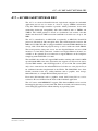
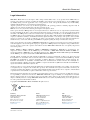
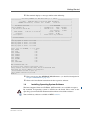
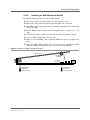
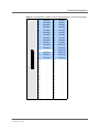
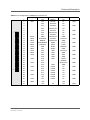
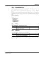
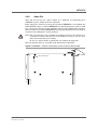
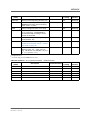
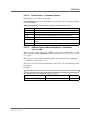
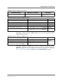
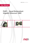
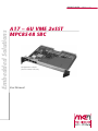
A17 – 6U VME 2eSST
MPC8548 SBC
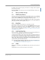
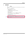
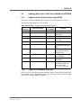
Configuration example
(shown without heat sink)
User Manual
®
A17 – 6U VME 2eSST MPC8548 SBC
A17 – 6U VME 2eSST MPC8548 SBC
The A17 is an advanced PowerPC® based single-board computer for embedded
applications and can act as a master or a slave in a legacy VMEbus environment.
Using the TSI148 bridge controller it provides 2eSST performance levels while
maintaining backwards compatibility with older standards such as VME64 and
VME32. The 2eSST protocol is based on synchronous data transfer and thus
doubles the theoretical VME transaction bandwidth to transfer rates of up to 320
MB/s.
The A17 is controlled by an MPC8548, or optionally an MPC8543 PowerPC®
processor (alternatively with encryption unit) with clock frequencies between 800
MHz and 1.5 GHz. The SBC is equipped with ECC-controlled DDR2 RAM for data
storage, with a Flash disk for program storage as well as with non-volatile FRAM.
The board provides front-panel access for two Gigabit Ethernet and two COM
interfaces via four RJ45 connectors. Another two Gigabit Ethernet channels are
available at the optional P0 rear connector to support Ethernet on the backplane
complying with ANSI/VITA 31.1-2003.
The two PMC slots on the A17 support PMC modules working with 32-bit/33-MHz
up to 64-bit/66-MHz. One of the mezzanine slots supports rear I/O and can also be
used for XMC modules with a PCI Express® x1, x2, or x4 link. The second (PMC
only) slot is connected to the onboard FPGA and can thus act as the physical layer
for additional functions implemented in the FPGA. The PMC/XMC slots allow
flexible extension to the A17, adding functions such as graphics, mass storage,
further Ethernet, or a simple FPGA-backed physical layer.
Even more I/O functions such as graphics, touch, CAN, binary I/O etc. can be
realized as IP cores in FPGA for the needs of the individual application.
The A17 comes with MENMON™ support. This firmware/BIOS can be used for
bootstrapping operating systems (from disk, Flash or network), for hardware testing,
or for debugging applications without running any operating system.
MEN Mikro Elektronik GmbH
20A017-00 E4 – 2010-11-22
2
Technical Data
Technical Data
CPU
• PowerPC® PowerQUICC™ III MPC8548, MPC8548E, MPC8543 or
MPC8543E
- 800 MHz up to 1.5 GHz
- Please see Configuration Options for available standard versions.
- e500 PowerPC® core with MMU and double-precision embedded scalar and
vector floating-point APU
- Integrated Northbridge and Southbridge
Memory
• 2x32 KB L1 data and instruction cache, 512 KB/256 KB L2 cache integrated in
MPC8548/MPC8543
• Up to 2 GB SDRAM system memory
- Soldered
- DDR2 with or without ECC
- Up to 300 MHz memory bus frequency, depending on CPU
• Up to 4 GB soldered Flash disk (SSD solid state disk)
- Higher capacity possible when components are available
- FPGA-controlled
• Up to hardware revision 02.xx: 32 MB additional DDR2 SDRAM, FPGA-controlled, e.g. for video data
• 16 MB boot Flash
• 128 KB non-volatile FRAM
• Serial EEPROM 8 kbits for factory settings
Mass Storage
• Up to 4 GB soldered ATA Flash disk (SSD solid state disk)
- Higher capacity possible if components are available
- FPGA-controlled
I/O
• Ethernet
- Up to four 10/100/1000Base-T Ethernet channels
- Two RJ45 connectors at front panel
- Two front LEDs per channel to signal LAN Link and Activity
- Two channels accessible via rear I/O on connector P0 complying with ANSI/
VITA 31.1-2003 (option)
• Two RS232 UARTs (COM1/2)
- Two RJ45 connectors at front panel
- Data rates up to 115.2 kbits/s
- 16-byte transmit/receive buffer
- Handshake lines: CTS, RTS
• GPIO
- 31 GPIO lines
- FPGA-controlled
- Connection via PMC1 board-to-board connector J4
MEN Mikro Elektronik GmbH
20A017-00 E4 – 2010-11-22
3
Technical Data
Front Connections
• Two Ethernet (RJ45)
• COM1/COM2 (RJ45)
• XMC/PMC 0 and PMC 1
Rear I/O
• Two 10/100/1000Base-T Ethernet on P0 (option)
• Mezzanine rear I/O: PMC 0 on P2
Mezzanine Slots
• Two slots total, one slot usable for PMC or XMC
• One XMC slot
- Compliant with XMC standard VITA 42.3-2006
- PCI Express® links: one x1 or one x2 or one x4
• Two PMC slots
- Compliant with PMC standard IEEE 1386.1
- Up to 64-bit/64-MHz, 3.3 V V(I/O)
- PMC I/O module (PIM) support through J4 complying with VITA 35 (PMC 0)
Miscellaneous
•
•
•
•
Real-time clock with battery backup
Temperature sensor, power supervision and watchdog
Reset button in ejector handle
One power good LED, three user-configurable LEDs at front
Local PCI Bus
• 64-bit/66-MHz, 3.3 V V(I/O)
• Compliant with PCI Specification 2.2
VMEbus
•
•
•
•
•
•
•
•
•
•
•
•
•
•
TSI148 controller
Compliant with VME64 Specification
Supports VME32, VME64, 2eVME and 2eSST (VITA 1.5)
Slot-1 function with auto-detection
Master
- D08:D16:D32:D64:A16:A24:A32:A64:BLT:MBLT:RMW
Slave
- D08:D16:D32:D64:A16:A24:A32:A64:BLT:MBLT
DMA
Mailbox functionality
Bus timer
Location Monitor
Interrupter D08(O):I(7-1):ROAK
Interrupt handler D08(O):IH(7-1)
Single level 3 fair requester
Single level 3 arbiter
MEN Mikro Elektronik GmbH
20A017-00 E4 – 2010-11-22
4
Technical Data
Electrical Specifications
• Supply voltage/power consumption:
- +5 V (-3%/+5%), approx. 2.2 A
- +3.3 V (-3%/+5%), approx. 1.1 A
- +12 V (-5%/+5%), only provided for PMCs that need 12 V
- -12 V (-5%/+5%), only provided for PMCs that need 12 V
Mechanical Specifications
• Dimensions: standard double Eurocard, 233.3 mm x 160 mm
• Weight: 490 g (incl. heat sink, without XMC/PMC modules)
Environmental Specifications
• Temperature range (operation):
- -40..+85°C (screened)
- Airflow: min. 10 m³/h
• Temperature range (storage): -40..+85°C
• Relative humidity (operation): max. 95% non-condensing
• Relative humidity (storage): max. 95% non-condensing
• Altitude: -300 m to +3,000 m
• Shock: 15 g, 11 ms
• Bump: 10 g, 16 ms
• Vibration (sinusoidal): 1 g, 10..150 Hz
• Conformal coating on request
MTBF
• 220,017 h @ 40°C according to IEC/TR 62380 (RDF 2000)
Safety
• PCB manufactured with a flammability rating of 94V-0 by UL recognized manufacturers
EMC
• Conforming to EN 55022 (radio disturbance), IEC1000-4-2 (ESD) and
IEC1000-4-4 (burst) with regard to CE conformity
BIOS
• MENMON™
Software Support
•
•
•
•
•
Linux
VxWorks®
QNX® (on request; support of the FPU is currently not provided by QNX®)
OS-9® (on request)
For more information on supported operating system versions and drivers see
online data sheet.
MEN Mikro Elektronik GmbH
20A017-00 E4 – 2010-11-22
5
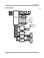
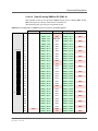
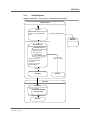
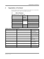
Block Diagram
Block Diagram
System
SDRAM
DDR2
EEPROM
RTC
Boot
Flash
FRAM
Watchdog
Ethernet
1000Base-T
Ethernet
1000Base-T
PowerPC®
MPC8548 or
MPC8543
F
F
Ethernet
1000Base-T
Ethernet
1000Base-T
VME
P0
RS232 COM1
F
RS232 COM2
F
32-bit
R
F
Front connector
R
Rear I/O connector
Options
FPGA
Flash Disk
SSD
Option: User I/O
I/O
PCI
e
J4
PCI
64-bit
64-bit
x8
64-bit
MEN Mikro Elektronik GmbH
20A017-00 E4 – 2010-11-22
PMC 1
F
Shared slot
PMC0 or
XMC
PCI-toVMEbus
Bridge
F
VME
P2
R
VME
P1
6
Configuration Options
Configuration Options
CPU
• Several PowerQUICC™ III types with different clock frequencies
• MPC8548 or MPC8548E
- 1 GHz, 1.2 GHz, 1.33 GHz or 1.5 GHz
• MPC8543 or MPC8543E
- 800 MHz or 1 GHz
Memory
• System RAM
- 512 MB, 1 GB or 2 GB
- With or without ECC
• Flash Disk
- 0 GB up to 4 GB (and more, if components are available)
• FRAM
- 0 KB or 128 KB
I/O
• Ethernet
- Two additional Gigabit Ethernet channels on VMEbus P0 rear connector for
ANSI/VITA 31.1-2003 support (only with MPC8548)
- Only two channels (at front) instead of four with MPC8543
• PCI Express® links: one x8 link
- Reduces operation temperature range because of higher DDR SDRAM clock
FPGA
• The onboard FPGA offers the possibility to add customized I/O functionality.
• FPGA Altera® Cyclone™ II EP2C35
- 33,216 logic elements
- 483,840 total RAM bits
• Connection
- Total available pin count: 31 pins
- Functions available via PMC slot 1 connector Pn4
• You can find more information on our web page "User I/O in FPGA"
VMEbus
• Single 5V supply for operation in VME32 systems
Please note that some of these options may only be available for large volumes.
Please ask our sales staff for more information.
For available standard configurations see online data sheet.
MEN Mikro Elektronik GmbH
20A017-00 E4 – 2010-11-22
7
Product Safety
Product Safety
!
Lithium Battery
This board contains a lithium battery. There is a danger of explosion if the
battery is incorrectly replaced!
See Chapter 5 Maintenance on page 69.
!
Electrostatic Discharge (ESD)
Computer boards and components contain electrostatic sensitive devices.
Electrostatic discharge (ESD) can damage components. To protect the board and
other components against damage from static electricity, you should follow some
precautions whenever you work on your computer.
• Power down and unplug your computer system when working on the inside.
• Hold components by the edges and try not to touch the IC chips, leads, or circuitry.
• Use a grounded wrist strap before handling computer components.
• Place components on a grounded antistatic pad or on the bag that came with the
component whenever the components are separated from the system.
• Store the board only in its original ESD-protected packaging. Retain the original
packaging in case you need to return the board to MEN for repair.
MEN Mikro Elektronik GmbH
20A017-00 E4 – 2010-11-22
8
About this Document
About this Document
This user manual describes the hardware functions of the board, connection of
peripheral devices and integration into a system. It also provides additional
information for special applications and configurations of the board.
The manual does not include detailed information on individual components (data
sheets etc.). A list of literature is given in the appendix.
History
Issue
Comments
Date
E1
First edition
2008-02-25
E2
MTBF added; P0 pinout corrected; MENMON chapter
and description of reset behavior corrected
2008-07-28
E3
System parameter vme_irq added; note on J4 on PMC
1 added; minor corrections
2008-11-27
E4
Changes for removed FPGA-controlled DRAM as of
hardware rev. 03.xx; minor errors corrected
2010-11-22
Conventions
!
italics
bold
monospace
hyperlink
This sign marks important notes or warnings concerning proper functionality of the
product described in this document. You should read them in any case.
Folder, file and function names are printed in italics.
Bold type is used for emphasis.
A monospaced font type is used for hexadecimal numbers, listings, C function
descriptions or wherever appropriate. Hexadecimal numbers are preceded by "0x".
Hyperlinks are printed in blue color.
The globe will show you where hyperlinks lead directly to the Internet, so you can
look for the latest information online.
IRQ#
/IRQ
Signal names followed by "#" or preceded by a slash ("/") indicate that this signal is
either active low or that it becomes active at a falling edge.
in/out
Signal directions in signal mnemonics tables generally refer to the corresponding
board or component, "in" meaning "to the board or component", "out" meaning
"coming from it".
Vertical lines on the outer margin signal technical changes to the previous edition of
the document.
MEN Mikro Elektronik GmbH
20A017-00 E4 – 2010-11-22
9
About this Document
Legal Information
MEN Mikro Elektronik reserves the right to make changes without further notice to any products herein. MEN makes no
warranty, representation or guarantee regarding the suitability of its products for any particular purpose, nor does MEN assume
any liability arising out of the application or use of any product or circuit, and specifically disclaims any and all liability,
including without limitation consequential or incidental damages.
"Typical" parameters can and do vary in different applications. All operating parameters, including "Typicals" must be
validated for each customer application by customer's technical experts.
MEN does not convey any license under its patent rights nor the rights of others.
Unless agreed otherwise, MEN products are not designed, intended, or authorized for use as components in systems intended
for surgical implant into the body, or other applications intended to support or sustain life, or for any other application in which
the failure of the MEN product could create a situation where personal injury or death may occur. Should Buyer purchase or
use MEN products for any such unintended or unauthorized application, Buyer shall indemnify and hold MEN and its officers,
employees, subsidiaries, affiliates, and distributors harmless against all claims, costs, damages, and expenses, and reasonable
attorney fees arising out of, directly or indirectly, any claim of personal injury or death associated with such unintended or
unauthorized use, even if such claim alleges that MEN was negligent regarding the design or manufacture of the part.
Unless agreed otherwise, the products of MEN Mikro Elektronik are not suited for use in nuclear reactors and for application
in medical appliances used for therapeutical purposes. Application of MEN products in such plants is only possible after the
user has precisely specified the operation environment and after MEN Mikro Elektronik has consequently adapted and
released the product.
ESM™, ESMini™, MDIS™, MDIS4™, MDIS5™, MENMON™, M-Module™, M-Modules™, SA-Adapter™, SAAdapters™, UBox™, USM™ and the MBIOS logo are trademarks of MEN Mikro Elektronik GmbH. PC-MIP® is a
registered trademark of MEN Micro, Inc. and SBS Technologies, Inc. MEN Mikro Elektronik®, ESMexpress®, MIPIOS®
and the MEN logo are registered trademarks of MEN Mikro Elektronik GmbH.
Altera®, Arria®, Avalon®, Cyclone®, Nios® and Quartus® are registered trademarks of Altera Corp. Freescale™ and
PowerQUICC™ are trademarks of Freescale Semiconductor, Inc. PowerPC® is a registered trademark of IBM Corp. OS-9®,
OS-9000® and SoftStax® are registered trademarks of RadiSys Microware Communications Software Division, Inc.
FasTrak™ and Hawk™ are trademarks of RadiSys Microware Communications Software Division, Inc. RadiSys® is a
registered trademark of RadiSys Corporation. QNX® is a registered trademark of QNX Ltd. Tornado® and VxWorks® are
registered trademarks of Wind River Systems, Inc.
All other products or services mentioned in this publication are identified by the trademarks, service marks, or product names
as designated by the companies who market those products. The trademarks and registered trademarks are held by the
companies producing them. Inquiries concerning such trademarks should be made directly to those companies. All other brand
or product names are trademarks or registered trademarks of their respective holders.
Information in this document has been carefully checked and is believed to be accurate as of the date of publication; however,
no responsibility is assumed for inaccuracies. MEN Mikro Elektronik accepts no liability for consequential or incidental
damages arising from the use of its products and reserves the right to make changes on the products herein without notice to
improve reliability, function or design. MEN Mikro Elektronik does not assume any liability arising out of the application or
use of the products described in this document.
Copyright © 2010 MEN Mikro Elektronik GmbH. All rights reserved.
Please recycle
Germany
MEN Mikro Elektronik GmbH
Neuwieder Straße 5-7
90411 Nuremberg
Phone +49-911-99 33 5-0
Fax +49-911-99 33 5-901
E-mail [email protected]
www.men.de
MEN Mikro Elektronik GmbH
20A017-00 E4 – 2010-11-22
France
MEN Mikro Elektronik SA
18, rue René Cassin
ZA de la Châtelaine
74240 Gaillard
Phone +33 (0) 450-955-312
Fax +33 (0) 450-955-211
E-mail [email protected]
www.men-france.fr
USA
MEN Micro, Inc.
24 North Main Street
Ambler, PA 19002
Phone (215) 542-9575
Fax (215) 542-9577
E-mail [email protected]
www.menmicro.com
10
Contents
Contents
1 Getting Started . . . . . . . . . . . . . . . . . . . . . . . . . . . . . . . . . . . . . . . . . . . . . . . .
1.1 Map of the Board. . . . . . . . . . . . . . . . . . . . . . . . . . . . . . . . . . . . . . . . .
1.2 Configuring the Hardware . . . . . . . . . . . . . . . . . . . . . . . . . . . . . . . . . .
1.3 Integrating the Board into a System . . . . . . . . . . . . . . . . . . . . . . . . . .
1.4 Installing Operating System Software. . . . . . . . . . . . . . . . . . . . . . . . .
16
16
17
17
18
2 Functional Description . . . . . . . . . . . . . . . . . . . . . . . . . . . . . . . . . . . . . . . . . .
2.1 Power Supply. . . . . . . . . . . . . . . . . . . . . . . . . . . . . . . . . . . . . . . . . . . .
2.2 Board Supervision . . . . . . . . . . . . . . . . . . . . . . . . . . . . . . . . . . . . . . . .
2.3 Clock Supply . . . . . . . . . . . . . . . . . . . . . . . . . . . . . . . . . . . . . . . . . . . .
2.4 Real-Time Clock . . . . . . . . . . . . . . . . . . . . . . . . . . . . . . . . . . . . . . . . .
2.5 Processor Core. . . . . . . . . . . . . . . . . . . . . . . . . . . . . . . . . . . . . . . . . . .
2.5.1
General . . . . . . . . . . . . . . . . . . . . . . . . . . . . . . . . . . . . . . . . .
2.5.2
Thermal Considerations . . . . . . . . . . . . . . . . . . . . . . . . . . . .
2.6 Bus Structure . . . . . . . . . . . . . . . . . . . . . . . . . . . . . . . . . . . . . . . . . . . .
2.6.1
Host-to-PCI Bridge . . . . . . . . . . . . . . . . . . . . . . . . . . . . . . . .
2.6.2
Local PCI Bus . . . . . . . . . . . . . . . . . . . . . . . . . . . . . . . . . . . .
2.6.3
PCI-to-VMEbus Bridge . . . . . . . . . . . . . . . . . . . . . . . . . . . .
2.6.4
PCI Express. . . . . . . . . . . . . . . . . . . . . . . . . . . . . . . . . . . . . .
2.7 Memory and Mass Storage . . . . . . . . . . . . . . . . . . . . . . . . . . . . . . . . .
2.7.1
DRAM System Memory . . . . . . . . . . . . . . . . . . . . . . . . . . . .
2.7.2
Boot Flash . . . . . . . . . . . . . . . . . . . . . . . . . . . . . . . . . . . . . . .
2.7.3
Solid State Flash Disk . . . . . . . . . . . . . . . . . . . . . . . . . . . . . .
2.7.4
FRAM . . . . . . . . . . . . . . . . . . . . . . . . . . . . . . . . . . . . . . . . . .
2.7.5
Additional SDRAM . . . . . . . . . . . . . . . . . . . . . . . . . . . . . . .
2.7.6
EEPROM. . . . . . . . . . . . . . . . . . . . . . . . . . . . . . . . . . . . . . . .
2.8 Ethernet Interfaces. . . . . . . . . . . . . . . . . . . . . . . . . . . . . . . . . . . . . . . .
2.8.1
Connection at Front. . . . . . . . . . . . . . . . . . . . . . . . . . . . . . . .
2.8.2
Connection at Rear . . . . . . . . . . . . . . . . . . . . . . . . . . . . . . . .
2.8.3
General . . . . . . . . . . . . . . . . . . . . . . . . . . . . . . . . . . . . . . . . .
2.8.4
10Base-T . . . . . . . . . . . . . . . . . . . . . . . . . . . . . . . . . . . . . . . .
2.8.5
100Base-T . . . . . . . . . . . . . . . . . . . . . . . . . . . . . . . . . . . . . . .
2.8.6
1000Base-T . . . . . . . . . . . . . . . . . . . . . . . . . . . . . . . . . . . . . .
2.9 UART Interfaces . . . . . . . . . . . . . . . . . . . . . . . . . . . . . . . . . . . . . . . . .
2.10 XMC Slot. . . . . . . . . . . . . . . . . . . . . . . . . . . . . . . . . . . . . . . . . . . . . . .
2.10.1 Connection . . . . . . . . . . . . . . . . . . . . . . . . . . . . . . . . . . . . . .
2.10.2 Installing an XMC Mezzanine Module. . . . . . . . . . . . . . . . .
2.11 PMC Slots . . . . . . . . . . . . . . . . . . . . . . . . . . . . . . . . . . . . . . . . . . . . . .
2.11.1 Installing a PMC Mezzanine Module . . . . . . . . . . . . . . . . . .
2.11.2 FPGA I/O through PMC1 J4. . . . . . . . . . . . . . . . . . . . . . . . .
2.12 Reset Button . . . . . . . . . . . . . . . . . . . . . . . . . . . . . . . . . . . . . . . . . . . .
2.13 Status and User LEDs . . . . . . . . . . . . . . . . . . . . . . . . . . . . . . . . . . . . .
2.14 VMEbus Interface . . . . . . . . . . . . . . . . . . . . . . . . . . . . . . . . . . . . . . . .
2.14.1 General . . . . . . . . . . . . . . . . . . . . . . . . . . . . . . . . . . . . . . . . .
2.14.2 Connection . . . . . . . . . . . . . . . . . . . . . . . . . . . . . . . . . . . . . .
19
19
19
19
19
20
20
20
21
21
21
21
21
22
22
22
22
22
23
23
24
24
25
25
25
26
26
27
28
28
30
31
32
33
35
35
36
36
37
MEN Mikro Elektronik GmbH
20A017-00 E4 – 2010-11-22
11
Contents
3 MENMON . . . . . . . . . . . . . . . . . . . . . . . . . . . . . . . . . . . . . . . . . . . . . . . . . . . .
3.1 General . . . . . . . . . . . . . . . . . . . . . . . . . . . . . . . . . . . . . . . . . . . . . . . .
3.1.1
State Diagram . . . . . . . . . . . . . . . . . . . . . . . . . . . . . . . . . . . .
3.2 Interacting with MENMON . . . . . . . . . . . . . . . . . . . . . . . . . . . . . . . .
3.2.1
Entering the Setup Menu/Command Line . . . . . . . . . . . . . .
3.3 Configuring MENMON for Automatic Boot . . . . . . . . . . . . . . . . . . .
3.4 Updating Boot Flash, SSD Flash, SDRAM and EEPROM. . . . . . . . .
3.4.1
Update via the Serial Console using SERDL . . . . . . . . . . . .
3.4.2
Update from Network using NDL. . . . . . . . . . . . . . . . . . . . .
3.4.3
Updating MENMON Code . . . . . . . . . . . . . . . . . . . . . . . . . .
3.5 Diagnostic Tests. . . . . . . . . . . . . . . . . . . . . . . . . . . . . . . . . . . . . . . . . .
3.5.1
Ethernet . . . . . . . . . . . . . . . . . . . . . . . . . . . . . . . . . . . . . . . . .
3.5.2
SDRAM and FRAM . . . . . . . . . . . . . . . . . . . . . . . . . . . . . . .
3.5.3
FPGA . . . . . . . . . . . . . . . . . . . . . . . . . . . . . . . . . . . . . . . . . .
3.5.4
EEPROM. . . . . . . . . . . . . . . . . . . . . . . . . . . . . . . . . . . . . . . .
3.5.5
SSD Flash Disk . . . . . . . . . . . . . . . . . . . . . . . . . . . . . . . . . . .
3.5.6
COM1/COM2 . . . . . . . . . . . . . . . . . . . . . . . . . . . . . . . . . . . .
3.5.7
RTC . . . . . . . . . . . . . . . . . . . . . . . . . . . . . . . . . . . . . . . . . . . .
3.6 MENMON Configuration and Organization . . . . . . . . . . . . . . . . . . . .
3.6.1
Consoles . . . . . . . . . . . . . . . . . . . . . . . . . . . . . . . . . . . . . . . .
3.6.2
Abort Pin . . . . . . . . . . . . . . . . . . . . . . . . . . . . . . . . . . . . . . . .
3.6.3
MENMON Memory Map . . . . . . . . . . . . . . . . . . . . . . . . . . .
3.6.4
MENMON BIOS Logical Units . . . . . . . . . . . . . . . . . . . . . .
3.6.5
System Parameters . . . . . . . . . . . . . . . . . . . . . . . . . . . . . . . .
3.7 MENMON Commands . . . . . . . . . . . . . . . . . . . . . . . . . . . . . . . . . . . .
42
42
43
45
45
45
46
46
46
47
48
48
49
50
50
51
51
52
53
53
54
55
56
57
63
4 Organization of the Board . . . . . . . . . . . . . . . . . . . . . . . . . . . . . . . . . . . . . . .
4.1 Address Mappings . . . . . . . . . . . . . . . . . . . . . . . . . . . . . . . . . . . . . . . .
4.2 Interrupt Handling . . . . . . . . . . . . . . . . . . . . . . . . . . . . . . . . . . . . . . . .
4.3 SMB Devices . . . . . . . . . . . . . . . . . . . . . . . . . . . . . . . . . . . . . . . . . . . .
4.4 PCI Devices on Bus 0 . . . . . . . . . . . . . . . . . . . . . . . . . . . . . . . . . . . . .
65
65
67
68
68
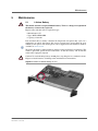
5 Maintenance . . . . . . . . . . . . . . . . . . . . . . . . . . . . . . . . . . . . . . . . . . . . . . . . . . 69
5.1 Lithium Battery . . . . . . . . . . . . . . . . . . . . . . . . . . . . . . . . . . . . . . . . . . 69
6 Appendix . . . . . . . . . . . . . . . . . . . . . . . . . . . . . . . . . . . . . . . . . . . . . . . . . . . . . 70
6.1 Literature and Web Resources . . . . . . . . . . . . . . . . . . . . . . . . . . . . . . . 70
6.1.1
PowerPC . . . . . . . . . . . . . . . . . . . . . . . . . . . . . . . . . . . . . . . . 70
6.1.2
Ethernet . . . . . . . . . . . . . . . . . . . . . . . . . . . . . . . . . . . . . . . . . 70
6.1.3
XMC/PMC . . . . . . . . . . . . . . . . . . . . . . . . . . . . . . . . . . . . . . 70
6.1.4
PCI Express. . . . . . . . . . . . . . . . . . . . . . . . . . . . . . . . . . . . . . 71
6.1.5
VMEbus . . . . . . . . . . . . . . . . . . . . . . . . . . . . . . . . . . . . . . . . 71
6.2 Finding out the Board’s Article Number, Revision and Serial Number71
MEN Mikro Elektronik GmbH
20A017-00 E4 – 2010-11-22
12
Figures
Figure 1.
Figure 2.
Figure 3.
Figure 4.
Figure 5.
Figure 6.
Figure 7.
Figure 8.
Figure 9.
MEN Mikro Elektronik GmbH
20A017-00 E4 – 2010-11-22
Map of the board – front panel and top view . . . . . . . . . . . . . . . . . . . .
Installing an XMC mezzanine module . . . . . . . . . . . . . . . . . . . . . . . . .
Installing a PMC mezzanine module . . . . . . . . . . . . . . . . . . . . . . . . . .
Position of reset button . . . . . . . . . . . . . . . . . . . . . . . . . . . . . . . . . . . . .
MENMON – State diagram, Degraded Mode/Full Mode . . . . . . . . . .
MENMON – State diagram, main state . . . . . . . . . . . . . . . . . . . . . . . .
MENMON – Position of abort pins on test connector (bottom side). .
Position of lithium battery on A17 . . . . . . . . . . . . . . . . . . . . . . . . . . . .
Labels giving the board’s article number, revision and serial number.
16
30
32
35
43
44
54
69
71
13
Tables
Table 1.
Table 2.
Table 3.
Table 4.
Table 5.
Table 6.
Table 7.
Table 8.
Table 9.
Table 10.
Table 11.
Table 12.
Table 13.
Table 14.
Table 15.
Table 16.
Table 17.
Table 18.
Table 19.
Table 20.
Table 21.
Table 22.
Table 23.
Table 24.
Table 25.
Table 26.
Table 27.
Table 28.
Table 29.
Table 30.
Table 31.
Table 32.
Table 33.
Table 34.
Table 35.
Table 36.
MEN Mikro Elektronik GmbH
20A017-00 E4 – 2010-11-22
Processor core options on A17 . . . . . . . . . . . . . . . . . . . . . . . . . . . . . . . 20
Pin assignment of 8-pin RJ45 Ethernet front connectors
(LAN1/LAN2) . . . . . . . . . . . . . . . . . . . . . . . . . . . . . . . . . . . . . . . . . . . 24
Signal mnemonics of Ethernet front interfaces . . . . . . . . . . . . . . . . . . 25
Pin assignment of 8-pin RJ45 UART front connectors
(COM1/COM2) . . . . . . . . . . . . . . . . . . . . . . . . . . . . . . . . . . . . . . . . . . 27
Signal mnemonics of UART front interfaces . . . . . . . . . . . . . . . . . . . . 27
Pin assignment of 114-pin XMC connector . . . . . . . . . . . . . . . . . . . . . 28
Signal mnemonics of 114-pin XMC connector . . . . . . . . . . . . . . . . . . 29
Assignment of 16Z034_GPIO controllers . . . . . . . . . . . . . . . . . . . . . . 33
Pin assignment of PMC1 board-to-board connector J4 (FPGA I/O
signals) . . . . . . . . . . . . . . . . . . . . . . . . . . . . . . . . . . . . . . . . . . . . . . . . . 34
Front-panel LEDs . . . . . . . . . . . . . . . . . . . . . . . . . . . . . . . . . . . . . . . . . 35
Pin assignment of VME64 bus connector P1 . . . . . . . . . . . . . . . . . . . . 38
Pin assignment of VMEbus rear I/O connector P2 (PMC signals) . . . 39
Signal mnemonics of VMEbus rear I/O connector P2 (PMC signals) . 40
Pin assignment of VMEbus rear I/O connector P0 (95-pin type "B"
modified) (Ethernet) . . . . . . . . . . . . . . . . . . . . . . . . . . . . . . . . . . . . . . . 41
Signal mnemonics of VMEbus rear I/O connector P0 (Ethernet) . . . . 41
MENMON – Program update files and locations . . . . . . . . . . . . . . . . 46
MENMON – Diagnostic tests: Ethernet. . . . . . . . . . . . . . . . . . . . . . . . 48
MENMON – Diagnostic tests: SDRAM and FRAM . . . . . . . . . . . . . . 49
MENMON – Diagnostic tests: FPGA . . . . . . . . . . . . . . . . . . . . . . . . . 50
MENMON – Diagnostic tests: EEPROM . . . . . . . . . . . . . . . . . . . . . . 50
MENMON – Diagnostic tests: SSD Flash disk . . . . . . . . . . . . . . . . . . 51
MENMON – Diagnostic tests: COM1/COM2 . . . . . . . . . . . . . . . . . . . 51
MENMON – Diagnostic tests: RTC. . . . . . . . . . . . . . . . . . . . . . . . . . . 52
MENMON – System parameters for console selection and
configuration. . . . . . . . . . . . . . . . . . . . . . . . . . . . . . . . . . . . . . . . . . . . . 53
MENMON – Address map (full-featured mode) . . . . . . . . . . . . . . . . . 55
MENMON – Boot Flash memory map . . . . . . . . . . . . . . . . . . . . . . . . 55
MENMON – Controller Logical Units (CLUNs). . . . . . . . . . . . . . . . . 56
MENMON – Device Logical Units (DLUNs) . . . . . . . . . . . . . . . . . . . 56
MENMON – A17 system parameters – Autodetected parameters. . . . 57
MENMON – A17 system parameters – Production data . . . . . . . . . . . 58
MENMON – A17 system parameters – MENMON persistent
parameters. . . . . . . . . . . . . . . . . . . . . . . . . . . . . . . . . . . . . . . . . . . . . . . 59
MENMON – A17 system parameters – VxWorks bootline parameters 61
MENMON – Reset causes through system parameter rststat. . . . . . . . 62
MENMON – Command reference . . . . . . . . . . . . . . . . . . . . . . . . . . . . 63
Memory map – processor view . . . . . . . . . . . . . . . . . . . . . . . . . . . . . . 65
Address mapping for PCI master . . . . . . . . . . . . . . . . . . . . . . . . . . . . . 65
14
Table 37.
Table 38.
Table 39.
Table 40.
Table 41.
Table 42.
Table 43.
Table 44.
MEN Mikro Elektronik GmbH
20A017-00 E4 – 2010-11-22
Address mapping for PCI slave . . . . . . . . . . . . . . . . . . . . . . . . . . . . . .
Address mapping for VMEbus master . . . . . . . . . . . . . . . . . . . . . . . . .
Address mapping for VMEbus slave . . . . . . . . . . . . . . . . . . . . . . . . . .
Dedicated interrupt line assignment . . . . . . . . . . . . . . . . . . . . . . . . . . .
Interrupt numbering assigned by MENMON (PCI) . . . . . . . . . . . . . . .
Interrupt numbering assigned by MENMON (PCIe) . . . . . . . . . . . . . .
SMB devices. . . . . . . . . . . . . . . . . . . . . . . . . . . . . . . . . . . . . . . . . . . . .
PCI devices on bus 0 . . . . . . . . . . . . . . . . . . . . . . . . . . . . . . . . . . . . . .
66
66
66
67
67
67
68
68
15
Getting Started
1
Getting Started
This chapter gives an overview of the board and some hints for first installation in a
system.
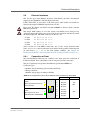
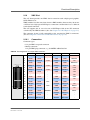
1.1
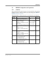
Map of the Board
Figure 1. Map of the board – front panel and top view
COM 1
Reset
button
User LEDs
COM 2
RTC with
Battery
Heat Sink
LAN 1
VMEbus P1
Power Good LED
MPC8548/43
LAN 2
20A017-00 E4 – 2010-11-22
J4 FPGA I/O
VMEbus P2
PMC / XMC
MEN Mikro Elektronik GmbH
XMC 0
3.3V
Voltage
Key
PMC0 / XMC
3.3V
Voltage
Key
J4 rear I/O
PMC
PMC1
VMEbus P0
TSI148
VMEbus
Bridge
16
Getting Started
1.2
Configuring the Hardware
You should check your hardware requirements before installing the board in a
system, since most modifications are difficult or even impossible to do when the
board is mounted in a rack.
The following check list gives an overview on what you might want to configure.
; XMC module
Refer to Chapter 2.10.2 Installing an XMC Mezzanine Module on page
30 for a detailed installation description.
; PMC modules
Refer to Chapter 2.11.1 Installing a PMC Mezzanine Module on page 32
for a detailed installation description.
1.3
Integrating the Board into a System
You can use the following check list when installing the board in a system for the
first time and with minimum configuration.
; Power-down the system.
; Remove all boards from the VMEbus system.
; Insert the A17 into slot 1 of the system, making sure that the VMEbus connectors are properly aligned.
; Connect a terminal to the RS232 interface COM1 (RJ45 connector).
(MEN offers an adapter cable with a standard 9-pin D-Sub plug connector.
Please see MEN’s website for ordering information.)
; Set your terminal to the following protocol:
-
9600 baud data transmission rate
8 data bits
1 stop bit
No parity
; Power-up the system.
MEN Mikro Elektronik GmbH
20A017-00 E4 – 2010-11-22
17
Getting Started
; The terminal displays a message similar to the following:
____________ Secondary MENMON for MEN EM9 Family 1.1 (A017) _________________
|
|
|
(c) 2007 - 2008 MEN Mikro Elektronik GmbH Nuremberg
|
|
MENMON 2nd Edition, Created Jan 9 2008
14:01:31
|
|_____________________________________________________________________________|
|
CPU Board: A017-00
|
CPU: MPC8548E
|
|Serial Number: 8
|
CPU/MEM Clk:
1320 / 264 MHz
|
| HW Revision: 00.01.00
|
CCB/LBC Clk:
528 / 66 MHz
|
|
|
PCI: 64 Bit / 33 MHz
|
|
DDR2 SDRAM:
1 GB ECC on 4.0/4/11|
FRAM: 128 kB
|
|
Produced:
|
FLASH:
16 MB
|
| Last repair:
|
Reset Cause: by software
|
|_____________________________________________________________________________|
| Carrier Board:
|
\___________________________________________________________________________/
Setting speed of NETIF 0 to AUTO
Setting speed of NETIF 1 to AUTO
Setting speed of NETIF 2 to AUTO
Setting speed of NETIF 3 to AUTO
press 'ESC' for MENMON, 's' for setup
Test SDRAM
: OK
Test FPGA
: OK
Test ETHER0
: OK
Test ETHER1
: OK
Test ETHER2
: OK
Test ETHER3
: OK
Test EEPROM
: OK
Test RTC
: OK
Test IDE0-NAND
: OK
NOW AUTOEXECUTING: BO
No default start address configured. Stop.
Setup network interface CLUN 0x02, 00:c0:3a:62:00:08 AUTO
Searching for server (BOOTP) in background
Telnet daemon started on port 23
HTTP daemon started on port 80
MenMon>
; Now you can use the MENMON BIOS/firmware (see detailed description in
Chapter 3 MENMON on page 42).
; Observe the installation instructions for the respective software.
1.4
Installing Operating System Software
The board supports Linux and VxWorks. QNX and OS-9 are available on request.
!
By standard, no operating system is installed on the board. Please refer to the
operating system installation documentation on how to install the software!
You can find any software available on MEN’s website.
MEN Mikro Elektronik GmbH
20A017-00 E4 – 2010-11-22
18
Functional Description
2
Functional Description
The following describes the individual functions of the board and their
configuration on the board. There is no detailed description of the individual
controller chips and the CPU. They can be obtained from the data sheets or data
books of the semiconductor manufacturer concerned (Chapter 6.1 Literature and
Web Resources on page 70).
2.1
Power Supply
The board is supplied with +5 V, +3.3 V and ±12 V via the VMEbus. However,
±12 V may be required only by some mezzanine modules.
The onboard power supply generates the 1.1 V core voltage for the CPU, 1.8 V for
memory and for the VMEbus bridge, 2.5 V for Ethernet, and the 1.2 V core voltage
for the FPGA.
2.2
Board Supervision
The board features a temperature sensor and voltage monitor.
The voltage monitor supervises 5V, 3.3V, 2.5V, 1.8V, 1.2V and 1.1V and holds the
CPU in reset condition until all supply voltages are within their nominal values.
In addition the board contains a PLD watchdog that must be triggered. After powerup the CPU loads the FPGA. After configuration the FPGA serves the PLD
watchdog without further action by the CPU. The watchdog timeout is
automatically set to 1.12 s after the first trigger pulse by the FPGA.
An additional watchdog is implemented in the FPGA itself. It can be enabled
through MENMON and can then be triggered by a software application. This
function is normally supported by the board support package (see BSP
documentation).
2.3
Clock Supply
The CPU is supplied with one copy of the onboard PCI clocks. This is internally
multiplied to generate the core clock and the memory clock.
By default the board runs at 66 MHz (PCI), 266 MHz (SDRAM memory) and
1.33 GHz (core).
2.4
Real-Time Clock
A battery-buffered real-time clock is integrated on the A17 CPU board. It is
accessed via I²C bus at address 0xD0. The voltage of the snap hat standby battery is
monitored by the RTC. A warning flag is set if the battery voltage falls below 2.5V.
The CPU can read this flag from bit D4 at word address 0x0F of the RTC. After
setting this flag the RTC continues operation for at least 1 month.
Interrupt generation of the RTC is not supported.
For details on maintenance of the snap-hat battery, see Chapter 5 Maintenance on
page 69.
MEN Mikro Elektronik GmbH
20A017-00 E4 – 2010-11-22
19
Functional Description
2.5
Processor Core
The board is equipped with the MPC8548 or MPC8543 processor, which includes a
32-bit PowerPC e500 core, the integrated host-to-PCI bridge, Ethernet controllers
and UARTs.
2.5.1
General
The MPC8548/3 family of processors integrates an e500v2 processor core built on
Power Architecture technology with system logic required for networking,
telecommunications, and wireless infrastructure applications. The MPC8548/3 is a
member of the PowerQUICC III family of devices that combine system-level
support for industry-standard interfaces with processors that implement the
embedded category of the Power Architecture technology.
The MPC8548/3 offers a double-precision floating-point auxiliary processing unit
(APU), up to 512 KB of level-2 cache, up to four integrated 10/100/1Gbits/s
enhanced three-speed Ethernet controllers with TCP/IP acceleration and
classification capabilities, a DDR/DDR2 SDRAM memory controller, a
programmable interrupt controller, two I²C controllers, a four-channel DMA
controller, a general-purpose I/O port, and dual universal asynchronous receiver/
transmitters (DUART).
The MPC8548/3 is available with (MPC8548/3E) or without an integrated security
engine with XOR acceleration.
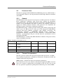
Table 1. Processor core options on A17
Processor Type
Core Frequency
L2 Cache
Encryption Unit
Ethernet Ports
MPC8548
1 GHz, 1.2 GHz, 1.33 GHz or
1.5 GHz
512 KB
No
4
MPC8548E
1 GHz, 1.2 GHz, 1.33 GHz or
1.5 GHz
512 KB
Yes
4
MPC8543
800 MHz or 1 GHz
256 KB
No
2
MPC8543E
800 MHz or 1 GHz
256 KB
Yes
2
2.5.2
Thermal Considerations
The CPU generates around 8 W of power dissipation when operated at 1.33 GHz.
To meet thermal requirements a suitable heat sink must be attached to the CPU and
sufficient airflow must be provided.
MEN provides a suitable heat sink to meet thermal requirements.
!
Please note that if you use any other heat sink than that supplied by MEN, or no heat
sink at all, warranty on functionality and reliability of the A17 may cease. If you
have any questions or problems regarding thermal behavior, please contact MEN.
MEN Mikro Elektronik GmbH
20A017-00 E4 – 2010-11-22
20
Functional Description
2.6
Bus Structure
2.6.1
Host-to-PCI Bridge
The integrated host-to-PCI bridge is used as host bridge and memory controller for
the PowerPC processor. All transactions of the PowerPC to the PCI bus are
controlled by the host bridge. The FRAM and boot Flash are connected to the local
memory bus of the integrated host-to-PCI bridge.
The PCI interface is PCI bus Rev. 2.2 compliant and supports all bus commands and
transactions. Master and target operations are possible. Only big-endian operation is
supported.
2.6.2
Local PCI Bus
The local PCI bus is controlled by the integrated host-to-PCI bridge. It runs at 66/
33 MHz.
The I/O voltage is fixed to 3.3 V. The data width is 64 bits.
The FPGA is connected to the local PCI bus.
2.6.3
PCI-to-VMEbus Bridge
The board has a standard TSI148 PCI-to-VME bridge for connection to the
VMEbus. On the local PCI bus this bridge is a master.
2.6.4
PCI Express
On A17 eight PCI Express lanes connect the XMC mezzanine module to the
PowerPC CPU. They can be used as one x1, one x2 or one x4 link. This means that
the XMC card implementation determines the usage of these eight lanes.
One x8 link is also possible on request, but this reduces the A17’s extended
operation temperature range.
2.6.4.1
PCI Express Basics
PCI Express (PCIe) succeeds PCI and AGP and offers higher data transfer rates.
As opposed to the PCI bus, PCIe is no parallel bus but a serial point-to-point
connection. Data is transferred using so-called lanes, with each lane consisting of a
line pair for transmission and a second pair for reception. Individual components are
connected using switches.
At the electrical level, each lane consists of two unidirectional LVDS (Low Voltage
Differential Signaling) pairs. Transmit and receive are separate differential pairs, for
a total of 4 data wires per lane.
PCIe supports full-duplex operation and uses a clock rate of 1.25 GHz. This results
in a data rate of max. 250 MB/s per lane in each direction. (The standard PCI bus
with 32 bits/33 MHz only allows a maximum of 133 MB/s.)
If you use only one lane, you speak of a PCIe x1 link. You can couple several lanes
to increase the data rate, e.g. x2 with 2 lanes up to a x32 link using 32 lanes.
MEN Mikro Elektronik GmbH
20A017-00 E4 – 2010-11-22
21
Functional Description
In addition, PCIe supports hot plug, for instance to exchange defect expansion
boards during operation.
In terms of software, most operating systems can handle PCI Express boards just as
well as the old PCI.
2.7
Memory and Mass Storage
2.7.1
DRAM System Memory
The board provides up to 2 GB onboard, soldered DDR2 (double data rate) SDRAM
on nine memory components (incl. ECC). The memory bus is 72 bits wide and
operates at up to 300 MHz (physical), depending on the processor type.
Depending on the board version the SDRAM may have ECC (error-correcting
code). ECC memory provides greater data accuracy and system uptime by
protecting against soft errors in computer memory.
2.7.2
Boot Flash
The board has 16 MB of onboard Flash. It is controlled by the CPU.
Flash memory contains the boot software for the MENMON/operating system
bootstrapper and application software. The MENMON sectors are softwareprotected against illegal write transactions through a password in the serial
download function of MENMON (cf. Chapter 3.4.1 Update via the Serial Console
using SERDL on page 46).
2.7.3
Solid State Flash Disk
The board includes a 2 GB soldered NAND Flash disk controlled by the FPGA. It is
accessed via an UltraDMA IDE controller located in the FPGA.
A solid state disk (SSD) is a data storage device that uses solid-state memory to
store persistent data. An SSD behaves like a conventional hard disk drive. On A17 it
has a PATA interface connected to the FPGA. With no moving parts, a solid state
disk is more robust, effectively eliminating the risk of mechanical failure, and
usually enjoys reduced seek time and latency by removing mechanical delays
associated with a conventional hard disk drive.
Note: If you would like to implement a hard disk on the A17 you can install a suitable PMC or XMC mezzanine module. (See also Chapter 2.10 XMC Slot on
page 28 and Chapter 2.11 PMC Slots on page 31.)
2.7.4
FRAM
The board has 128 KB non-volatile FRAM memory connected to the local bus of
the CPU.
The FRAM does not need a back-up voltage for data retention.
MEN Mikro Elektronik GmbH
20A017-00 E4 – 2010-11-22
22
Functional Description
2.7.5
Additional SDRAM
Up to hardware revision 03.xx of the A17, the board supports 32 MB additional
DDR2 SDRAM. It is controlled by the FPGA and can be used for graphics, for
instance.
!
From hardware revision 03.xx, the A17 no longer supports FPGA-controlled
additional SDRAM.
2.7.6
EEPROM
The board has an 8-kbit serial EEPROM for factory data, MENMON parameters
and for the VxWorks bootline.
MEN Mikro Elektronik GmbH
20A017-00 E4 – 2010-11-22
23
Functional Description
2.8
Ethernet Interfaces
The A17 has up to four Ethernet interfaces controlled by the CPU. All channels
support up to 1000 Mbits/s and full-duplex operation.
LAN1 and LAN2 are accessible at the front panel, while LAN3 and LAN4 are
routed to the optional VME P0 connector for rear I/O.
!
Please note that LAN3 and LAN4 are not available on board versions with the
MPC8543 processor.
!
The unique MAC address is set at the factory and should not be changed. Any
attempt to change this address may create node or bus contention and thereby render
the board inoperable. The MAC addresses on the A17 are:
•
•
•
•
LAN1:
LAN2:
LAN3:
LAN4:
0x 00 C0 3A 65 xx xx
0x 00 C0 3A 66 xx xx
0x 00 C0 3A 67 xx xx
0x 00 C0 3A 68 xx xx
where "00 C0 3A" is the MEN vendor code, "65" to "68" are the channel-related
codes, and "xx xx" is the hexadecimal serial number of the product, which depends
on your board, e. g. "... 00 2A" for serial number "000042". (See Chapter 6.2
Finding out the Board’s Article Number, Revision and Serial Number on page 71.)
2.8.1
Connection at Front
Two standard RJ45 connectors are available at the front panel for connection of
LAN1 and LAN2. Two status LEDs each are integrated into the connectors.
The pin assignments correspond to the Ethernet specification IEEE802.3.
Connector types:
• Modular 8/8-pin mounting jack according to FCC68
• Mating connector:
Modular 8/8-pin plug according to FCC68
Table 2. Pin assignment of 8-pin RJ45 Ethernet front connectors (LAN1/LAN2)
1000Base-T 10/100Base-T
Yellow:
Lights up whenever there is
receive activity
Green:
Lights up as soon as a
1000-Gbit link is established
MEN Mikro Elektronik GmbH
20A017-00 E4 – 2010-11-22
A
1
L
8
1
BI_DA+
TX+
2
BI_DA-
TX-
3
BI_DB+
RX+
4
BI_DC+
-
5
BI_DC-
-
6
BI_DB-
RX-
7
BI_DD+
-
8
BI_DD-
-
24
Functional Description
Table 3. Signal mnemonics of Ethernet front interfaces
Signal
Direction
Function
BI_D[A:D]+/- in/out
Differential pairs of data lines for 1000Base-T
RX+/-
in
Differential pair of receive data lines for 10/100Base-T
TX+/-
out
Differential pair of transmit data lines for 10/100Base-T
2.8.2
Connection at Rear
VMEbus connector P0 can be implemented as an option for Gigabit Ethernet
backplane I/O according to ANSI/VITA 31.1-2003. In this case, channels LAN3
and LAN4 are connected in compliance with ANSI/VITA 31.1-2003: LAN3 is
connected to LPa of the backplane and LAN4 is connected to LPb.
For the pin assignment please see Table 14, Pin assignment of VMEbus rear I/O
connector P0 (95-pin type "B" modified) (Ethernet), on page 41.
!
Please note that the P0 rear I/O option is not available on board versions with the
MPC8543(E) processor.
2.8.3
General
Ethernet is a local-area network (LAN) protocol that uses a bus or star topology and
supports data transfer rates of 100 Mbits/s and more. The Ethernet specification
served as the basis for the IEEE 802.3 standard, which specifies the physical and
lower software layers. Ethernet is one of the most widely implemented LAN
standards.
Ethernet networks provide high-speed data exchange in areas that require
economical connection to a local communication medium carrying bursty traffic at
high-peak data rates.
A classic Ethernet system consists of a backbone cable and connecting hardware
(e.g. transceivers), which links the controllers of the individual stations via
transceiver (transmitter-receiver) cables to this backbone cable and thus permits
communication between the stations.
2.8.4
10Base-T
10Base-T is one of several adaptations of the Ethernet (IEEE 802.3) standard for
Local Area Networks (LANs). The 10Base-T standard (also called Twisted Pair
Ethernet) uses a twisted-pair cable with maximum lengths of 100 meters. The cable
is thinner and more flexible than the coaxial cable used for the 10Base-2 or
10Base-5 standards. Since it is also cheaper, it is the preferable solution for costsensitive applications.
Cables in the 10Base-T system connect with RJ45 connectors. A star topology is
common with 12 or more computers connected directly to a hub or concentrator.
The 10Base-T system operates at 10 Mbits/s and uses baseband transmission methods.
MEN Mikro Elektronik GmbH
20A017-00 E4 – 2010-11-22
25
Functional Description
2.8.5
100Base-T
The 100Base-T networking standard supports data transfer rates up to 100 Mbits/s.
100Base-T is actually based on the older Ethernet standard. Because it is 10 times
faster than Ethernet, it is often referred to as Fast Ethernet. Officially, the 100Base-T
standard is IEEE 802.3u.
There are several different cabling schemes that can be used with 100Base-T, e.g.
100Base-TX, with two pairs of high-quality twisted-pair wires.
2.8.6
1000Base-T
1000Base-T is a specification for Gigabit Ethernet over copper wire (IEEE
802.3ab). The standard defines 1 Gbit/s data transfer over distances of up to 100
meters using four pairs of CAT-5 balanced copper cabling and a 5-level coding
scheme.
Because many companies already use CAT-5 cabling, 1000Base-T can be easily
implemented.
Other 1000Base-T benefits include compatibility with existing network protocols
(i.e. IP, IPX, AppleTalk), existing applications, Network Operating Systems,
network management platforms and applications.
MEN Mikro Elektronik GmbH
20A017-00 E4 – 2010-11-22
26
Functional Description
2.9
UART Interfaces
COM1 and COM2 are standard RS232 interfaces. They are available via two RJ45
connectors at the front panel.
COM1 is controlled by the MPC854X UART 0, COM2 is controlled by the
MPC854X UART 1.
Connector types:
• Modular 8/8-pin mounting jack according to FCC68
• Mating connector:
Modular 8/8-pin plug according to FCC68
Table 4. Pin assignment of 8-pin RJ45 UART front connectors (COM1/COM2)
1
8
1
-
2
-
3
-
4
GND
5
RXD
6
TXD
7
CTS
8
RTS
Table 5. Signal mnemonics of UART front interfaces
Signal
Function
CTS
in
Clear to send
GND
-
Ground
RTS
out
Request to send
RXD
in
Receive data
TXD
out
Transmit data
MEN Mikro Elektronik GmbH
20A017-00 E4 – 2010-11-22
Direction
27
Functional Description
2.10
XMC Slot
The A17 board provides one XMC slot for extension such as high-speed graphics,
SATA, Ethernet etc.
XMC modules have the same form factor as PMC modules, however they do not use
a PCI bus but a high-speed PCI Express connection and therefore have a different
carrier board connector.
The A17 supports one x1, one x2 or one x4 PCI Express link on one J15 connector
as defined by the XMC Standard. (See also Chapter 2.6.4 PCI Express on page 21.)
The connector layout is fully compatible to the standard for XMC.3 connectors.
(See also Chapter 6.1 Literature and Web Resources on page 70.)
2.10.1
Connection
Connector types:
• 114-pin XMC receptacle connector
• Mating connector:
114-pin XMC plug connector, e. g. SAMTEC ASP105885-01
Table 6. Pin assignment of 114-pin XMC connector
A B C D E F
1
2
19
A
B
C
D
E
F
1
PER0p0
PER0n0
+3.3V
PER0p1
PER0n1
+5V
2
GND
GND
-
GND
GND
MRSTI#
3
PER0p2
PER0n2
+3.3V
PER0p3
PER0n3
+5V
4
GND
GND
-
GND
GND
MRSTO#
5
PER0p4
PER0n4
+3.3V
PER0p5
PER0n5
+5V
6
GND
GND
-
GND
GND
+12V
7
PER0p6
PER0n6
+3.3V
PER0p7
PER0n7
+5V
8
GND
GND
-
GND
GND
-12V
9
-
-
-
-
-
+5V
10
GND
GND
-
GND
GND
GA0
11
PET0p0
PET0n0
-
PET0p1
PET0n1
+5V
12
GND
GND
GA1
GND
GND
-
13
PET0p2
PET0n2
-
PET0p3
PET0n3
+5V
14
GND
GND
GA2
GND
GND
MSDA
15
PET0p4
PET0n4
-
PET0p5
PET0n5
+5V
16
GND
GND
MVMRO
GND
GND
MSCL
17
PET0p6
PET0n6
-
PET0p7
PET0n7
-
18
GND
GND
-
GND
GND
-
-
WAKE#
ROOT0#
-
19
REFCLK+0 REFCLK-0
MEN Mikro Elektronik GmbH
20A017-00 E4 – 2010-11-22
28
Functional Description
Table 7. Signal mnemonics of 114-pin XMC connector
Signal
Power +12V, -12V
PCIe
Other
MEN Mikro Elektronik GmbH
20A017-00 E4 – 2010-11-22
Direction
Function
out
+12V supply voltage
+3.3V
out
+3.3V supply voltage
+5V (VPWR)
out
+5V supply voltage
GND
-
Ground
PER0p/n[0..7]
out
PCI Express lane, differential receive
PET0p/n[0..7]
in
PCI Express lane, differential transmit
REFCLK+/-0
out
Differential reference clock
ROOT0#
out
Root Complex enabling
WAKE#
out
Reactivation of power rails and reference
clocks
GA[0..2]
out
I²C channel select
MRSTI#
out
XMC reset in
MRSTO#
in
XMC reset out
MSCL
out
IPMI I²C serial clock
MSDA
in/out
IPMI I²C serial data
MVMRO
out
XMC write prohibit
29
Functional Description
2.10.2
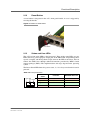
Installing an XMC Mezzanine Module
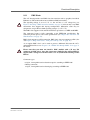
Perform the following steps to install an XMC module:
; Power down your system and remove the A17 from the system.
; Remove the filler panel from the board’s front XMC slot, if installed.
; The XMC module is plugged on the A17 with the component sides of the PCBs
facing each other.
; Put the XMC module’s front connector through the A17’s front slot at a 45°
angle.
; Carefully put it down, making sure that the connectors are properly aligned.
; Press the XMC module firmly onto the A17.
; Make sure that the EMC gasket around the XMC front panel is properly in its
place.
; Screw the XMC module tightly to the A17 using the two mounting standoffs
and four matching oval-head cross-recessed screws of type M2.5x6.
Figure 2. Installing an XMC mezzanine module
XMC module
Mounting
standoff
114-pin
connector
CPU board
2 M2.5x6 ovalhead crossrecessed screws
MEN Mikro Elektronik GmbH
20A017-00 E4 – 2010-11-22
2 M2.5x6 ovalhead crossrecessed screws
30
Functional Description
2.11
PMC Slots
The A17 board provides two PMC slots for extension such as graphics, hard disk,
Ethernet etc. The market offers lots of different PMC mezzanines.
!
The signaling voltage is set to 3.3 V, i. e. the A17 has a 3.3-V voltage key (see
Figure 3, Installing a PMC mezzanine module, on page 32) and can only carry PMC
mezzanines that support this keying configuration. Mezzanine cards may be
designed to accept either or both signaling voltages (3.3 V / 5 V).
The PMC slots support 32-bit and 64-bit PCI bus operation at 33 MHz or 66 MHz.
The connector layout is fully compatible to the IEEE1386 specification. For
connector pinouts please refer to the specification (see Chapter 6.1 Literature and
Web Resources on page 70).
PMC slot 0 supports rear I/O connection. PMC slot 1 does not support rear I/O! (See
also Figure 1, Map of the board – front panel and top view, on page 16.)
As an option PMC slot 1 can be used to process additional I/O from the A17’s
onboard FPGA. Please see Chapter 2.11.2 FPGA I/O through PMC1 J4 on page 33
for details.
!
Please note that you must not install a PMC module with a J4 rear I/O
connector in PMC slot 1, since this connector is linked to the onboard FPGA.
Signals with a voltage level of more than 3.3 V on J4 will lead to damage of the
FPGA!
Connector types:
• 64-pin, 1-mm pitch board-to-board receptacle according to IEEE 1386
• Mating connector:
64-pin, 1-mm pitch board-to-board plug according to IEEE 1386
MEN Mikro Elektronik GmbH
20A017-00 E4 – 2010-11-22
31
Functional Description
2.11.1
Installing a PMC Mezzanine Module
Perform the following steps to install a PMC module:
; Make sure that the voltage keying of your PMC module matches the A17.
; Power down your system and remove the A17 from the system.
; Remove the filler panel from the board’s front PMC slot, if installed.
; The PMC module is plugged on the A17 with the component sides of the PCBs
facing each other.
; Put the PMC module’s front connector through the A17’s front slot at a 45°
angle.
; Carefully put it down, making sure that the connectors are properly aligned.
; Press the PMC module firmly onto the A17.
; Make sure that the EMC gasket around the PMC front panel is properly in its
place.
; Screw the PMC module tightly to the A17 using the four mounting standoffs
and four matching oval-head cross-recessed screws of type M2.5x6.
Figure 3. Installing a PMC mezzanine module
PMC module
Mounting
standoff
3.3V
voltage key
64-pin
connectors
CPU board
2 M2.5x6 ovalhead crossrecessed screws
MEN Mikro Elektronik GmbH
20A017-00 E4 – 2010-11-22
2 M2.5x6 ovalhead crossrecessed screws
32
Functional Description
2.11.2
FPGA I/O through PMC1 J4
The FPGA on board the A17 leaves room for flexible I/O extensions to the board.
31 signal lines are connected from the FPGA to the PMC 1 slot’s J4 connector. The
lines are free for customized functions such as LVDS, IDE, graphics, GPIOs,
UARTs or fieldbus interfaces.
A plug-on board in PMC format – but without the need for actual PMC functionality
– can then be used as a physical layer to implement front-panel I/O connectors or an
onboard hard disk.
MEN offers a great variety of ready-to-implement IP core functions for the A17
FPGA. You can find an overview and descriptions of available standard FPGA IP
cores on MEN’s website.
Please note that with regard to the FPGA resources such as available logic elements
or pins it is not possible to grant all possible combinations of FPGA IP cores.
Please ask our sales staff for configuration possibilities.
By standard, GPIO lines are routed to the J4 connector. Four GPIO controllers
(MEN 16Z034_GPIO) are included in the FPGA to provide 31 GPIO lines. Voltage
levels are LVTTL.
You can control the GPIO lines through software using MDIS driver software
available on MEN’s website. The following table gives the assignment of the GPIO
controllers implemented in the A17’s FPGA to their function on the board.
Normally you can identify the controllers by their instance numbers in your
operating system.
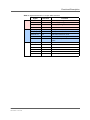
Table 8. Assignment of 16Z034_GPIO controllers
Instance
!
1
GPIO (lines 0 to 7) (bits 0..7)
2
GPIO (lines 8 to15) (bits 0..7)
3
GPIO (lines 16 to 23) (bits 0..7)
4
GPIO (lines 24 to 30) (bits 0..6)
By default all GPIOs are configured as inputs, so that there are no conflicts with
PMC P4 signals if you use a PMC with a P4 connector unless you reconfigure the
GPIO direction by software.
MEN Mikro Elektronik GmbH
20A017-00 E4 – 2010-11-22
Function
33
Functional Description
Table 9. Pin assignment of PMC1 board-to-board connector J4 (FPGA I/O signals)
1
63
MEN Mikro Elektronik GmbH
20A017-00 E4 – 2010-11-22
2
64
1
GPIO[30]
2
GPIO[0]
3
GPIO[29]
4
GPIO[1]
5
GPIO[28]
6
GPIO[2]
7
GPIO[27]
8
GPIO[3]
9
GPIO[26]
10
GPIO[4]
11
GPIO[25]
12
GPIO[5]
13
GPIO[24]
14
GPIO[6]
15
GPIO[23]
16
GPIO[7]
17
GPIO[22]
18
GPIO[8]
19
GPIO[21]
20
GPIO[9]
21
GPIO[10]
22
GPIO[11]
23
GPIO[12]
24
GPIO[13]
25
-
26
GPIO[14]
27
GPIO[15]
28
GPIO[16]
29
GPIO[17]
30
GPIO[18]
31
GPIO[19]
32
GPIO[20]
33
-
34
-
35
-
36
-
37
-
38
-
39
-
40
-
41
-
42
-
43
-
44
-
45
-
46
-
47
-
48
-
49
-
50
-
51
-
52
-
53
-
54
-
55
-
56
-
57
-
58
-
59
-
60
-
61
-
62
-
63
-
64
-
34
Functional Description
2.12
Reset Button
A reset button is integrated in the A17’s front panel handle. A reset is triggered by
releasing the handle.
Figure 4. Position of reset button
Reset button
2.13
Status and User LEDs
The A17 has four status LEDs at the front panel. Three of the status LEDs are user
LEDs driven by general-purpose output pins of the MPC854X. Programming these
signals as outputs and driving them to logic 0 means the LED is turned on. You can
control the GPIO lines through dedicated functions provided by MEN’s board
support packages (BSPs). The implementation and usage depend on the operating
system.
The Power Good LED shows the power status, i.e. it is always on when the board is
powered.
Table 10. Front-panel LEDs
LED No. /
Color
User LEDs
1
2 3 Power
COM 1
MEN Mikro Elektronik GmbH
20A017-00 E4 – 2010-11-22
COM 2
Function
MPC854X GPO Pin
1 - red
User LED
GPOUT29
2 - yellow
User LED
GPOUT28
3 - green
User LED
GPOUT27
4 - red
Power Good LED
-
35
Functional Description
2.14
VMEbus Interface
2.14.1
General
The A17's VMEbus interface conforms to the VME64 specification. It uses the
TSI148 controller as a PCI-to-VMEbus bridge.
The TSI148 is currently the highest bandwidth VME bridge available, providing
PCI-X-to-VME 2eSST performance levels while maintaining backwards
compatibility with older standards.
TSI148’s decoupled architecture and proper buffer sizing allows a very large
number of simultaneous transactions to take place. TSI148 is also a full featured
master, slave and system controller which allows it to be used in any VME
application.
Main features:
•
•
•
•
•
•
•
•
•
•
•
•
•
Supports VME32, VME64, 2eVME and 2eSST (VITA 1.5)
Slot-1 function with auto-detection
Master: D08:D16:D32:D64:A16:A24:A32:A64:BLT:MBLT:RMW
Slave: D08:D16:D32:D64:A16:A24:A32:A64:BLT:MBLT
DMA
Mailbox functionality
Bus timer
Location Monitor
Interrupter D08(O):I(7-1):ROAK
Interrupt handler D08(O):IH(7-1)
Single level 3 fair requester
Single level 3 arbiter
Low power consumption
Since the TSI148 controller is a very complex component, we have not included
any details on register access etc. here. Please refer to the bridge’s manufacturer
data sheet, which is available from the manufacturer’s website:
www.tundra.com/?genId=TSI148&cid=18698888
For more literature on the VMEbus see Chapter 6.1 Literature and Web
Resources on page 70.
MEN Mikro Elektronik GmbH
20A017-00 E4 – 2010-11-22
36
Functional Description
2.14.2
Connection
Connector types:
• 160-pin, 5-row plug, performance level according to DIN41612, part 5
• Mating connector:
160-pin, 5-row receptacle, performance level according to DIN41612, part 5
2.14.2.1 Bus Connection: VMEbus P1
The pin assignment of P1 conforms to the VME64 specification ANSI/VITA 1-1994
(R2002) and VME64 Extensions Standard ANSI/VITA 1.1-1997 (R2003).
MEN Mikro Elektronik GmbH
20A017-00 E4 – 2010-11-22
37
Functional Description
Table 11. Pin assignment of VME64 bus connector P1
DCB A Z
1
32
1
2
3
4
5
6
7
8
9
10
11
12
13
14
15
16
17
18
19
20
21
22
23
24
25
26
27
28
29
30
31
32
MEN Mikro Elektronik GmbH
20A017-00 E4 – 2010-11-22
D
GND
GAP#
GA0#
GA1#
+3.3V
GA2#
+3.3V
GA3#
+3.3V
GA4#
+3.3V
+3.3V
+3.3V
+3.3V
+3.3V
+3.3V
+3.3V
GND
-
C
D8
D9
D10
D11
D12
D13
D14
D15
GND
SYSFAIL#
BERR#
SYSRESET#
LWORD#
AM5
A23
A22
A21
A20
A19
A18
A17
A16
A15
A14
A13
A12
A11
A10
A9
A8
+12V
+5V
B
BBSY#
BCLR#
ACFAIL#
BG0IN#
BG0OUT#
BG1IN#
BG1OUT#
BG2IN#
BG2OUT#
BG3IN#
BG3OUT#
BR0#
BR1#
BR2#
BR3#
AM0
AM1
AM2
AM3
GND
GND
IRQ7#
IRQ6#
IRQ5#
IRQ4#
IRQ3#
IRQ2#
IRQ1#
+5V
A
D0
D1
D2
D3
D4
D5
D6
D7
GND
SYSCLK
GND
DS1#
DS0#
WRITE#
GND
DTACK#
GND
AS#
GND
IACK#
IACKIN#
IACKOUT#
AM4
A7
A6
A5
A4
A3
A2
A1
-12V
+5V
Z
GND
GND
GND
GND
GND
GND
GND
GND
GND
GND
GND
GND
GND
GND
GND
GND
38
Functional Description
2.14.2.2 Rear I/O using VMEbus P2 (PMC 0)
The standard version of A17 provides VME64 signals and rear I/O for PMC 0. The
PMC I/O signals are directly connected to connector P2.
The following table gives the pin assignment for P2.
Table 12. Pin assignment of VMEbus rear I/O connector P2 (PMC signals)
DCB A Z
1
32
D
C
B
A
Z
1
-
PMC0_J4.1
+5V
PMC0_J4.2
-
2
-
PMC0_J4.3
GND
PMC0_J4.4
GND
3
-
PMC0_J4.5
RETRY#
PMC0_J4.6
-
4
-
PMC0_J4.7
A24
PMC0_J4.8
GND
5
-
PMC0_J4.9
A25
PMC0_J4.10
-
6
-
PMC0_J4.11
A26
PMC0_J4.12
GND
7
-
PMC0_J4.13
A27
PMC0_J4.14
-
8
-
PMC0_J4.15
A28
PMC0_J4.16
GND
9
-
PMC0_J4.17
A29
PMC0_J4.18
-
10
-
PMC0_J4.19
A30
PMC0_J4.20
GND
11
-
PMC0_J4.21
A31
PMC0_J4.22
-
12
-
PMC0_J4.23
GND
PMC0_J4.24
GND
13
-
PMC0_J4.25
+5V
PMC0_J4.26
-
14
-
PMC0_J4.27
D16
PMC0_J4.28
GND
15
-
PMC0_J4.29
D17
PMC0_J4.30
-
16
-
PMC0_J4.31
D18
PMC0_J4.32
GND
17
-
PMC0_J4.33
D19
PMC0_J4.34
-
18
-
PMC0_J4.35
D20
PMC0_J4.36
GND
19
-
PMC0_J4.37
D21
PMC0_J4.38
-
20
-
PMC0_J4.39
D22
PMC0_J4.40
GND
21
-
PMC0_J4.41
D23
PMC0_J4.42
-
22
-
PMC0_J4.43
GND
PMC0_J4.44
GND
23
-
PMC0_J4.45
D24
PMC0_J4.46
-
24
-
PMC0_J4.47
D25
PMC0_J4.48
GND
25
-
PMC0_J4.49
D26
PMC0_J4.50
-
26
-
PMC0_J4.51
D27
PMC0_J4.52
GND
27
-
PMC0_J4.53
D28
PMC0_J4.54
-
28
-
PMC0_J4.55
D29
PMC0_J4.56
GND
29
-
PMC0_J4.57
D30
PMC0_J4.58
-
30
-
PMC0_J4.59
D31
PMC0_J4.60
GND
31
GND
PMC0_J4.61
GND
PMC0_J4.62
-
32
-
PMC0_J4.63
+5V
PMC0_J4.64
GND
MEN Mikro Elektronik GmbH
20A017-00 E4 – 2010-11-22
39
Functional Description
Table 13. Signal mnemonics of VMEbus rear I/O connector P2 (PMC signals)
Signal
Power
VME64
PMC 0
MEN Mikro Elektronik GmbH
20A017-00 E4 – 2010-11-22
Direction
Function
+5V
-
+5V power supply
GND
-
Digital ground
A[31:24]
in/out
VME64 address lines
D[31:16]
in/out
VME64 data lines
RETRY#
out
VME64 retry for postponed data transfer
PMC0_J4.xx
in/out
Signal xx from PMC 0 rear I/O connector
J4
40
Functional Description
2.14.2.3 Rear I/O using VMEbus P0 (Ethernet)
As an option the A17 provides backplane Ethernet through VMEbus connector P0.
In this case the two additional Gigabit channels LAN3 and LAN4 are accessible at
the rear. The two link ports are connected in compliance with ANSI/VITA 31.12003: LAN3 is connected to LPa of the backplane and LAN4 is connected to LPb.
The following table gives the pin assignment for P0.
Table 14. Pin assignment of VMEbus rear I/O connector P0 (95-pin type "B" modified) (Ethernet)
F E D C B A
1
2
19
F
E
D
C
B
A
1
GND
-
-
-
-
-
2
GND
LPa_DC-
LPa_DC+
GND
LPa_DA-Txa
LPa_DA+
+Txa
3
GND
LPa_DD-
LPa_DD+
GND
LPa_DB-Rxa
LPa_DB+
+Rxa
4
GND
LPb_DC-
LPb_DC+
GND
LPb_DA-Txb
LPb_DA+
+Txb
5
GND
LPb_DD-
LPb_DD+
GND
LPb_DB-Rxb
LPb_DB+
+Rxb
6
GND
-
-
-
-
-
7
GND
-
-
-
-
-
..
GND
-
-
-
-
-
19
GND
-
-
-
-
-
Table 15. Signal mnemonics of VMEbus rear I/O connector P0 (Ethernet)
Signal
Function
Power
GND
-
Digital ground
Ethernet
LAN3/4
LPa_D[A:D]+/-
in/out
Differential pairs of data lines for
1000Base-T in compliance with ANSI/
VITA 31.1-2003, LAN3
LPb_D[A:D]+/-
in/out
Differential pairs of data lines for
1000Base-T in compliance with ANSI/
VITA 31.1-2003, LAN4
+/-RXa, +/-TXa
in/out
Differential pairs of data lines for 10/
100Base-T, LAN3
+/-RXb, +/-TXb
in/out
Differential pairs of data lines for 10/
100Base-T, LAN4
MEN Mikro Elektronik GmbH
20A017-00 E4 – 2010-11-22
Direction
41
MENMON
3
MENMON
3.1
General
MENMON is the CPU board firmware that is invoked when the system is powered
on.
The basic tasks of MENMON are:
•
•
•
•
•
•
•
•
•
Initialize the CPU and its peripherals.
Load the FPGA code.
Set VMEbus bridge inbound/outbound windows.
PCI auto configuration.
Perform self-test.
Provide debug/diagnostic features on MENMON command line.
Interaction with the user via touch panel/TFT display.
Boot operating system.
Update firmware or operating system.
The following description only includes board-specific features. For a general
description and in-depth details on MENMON, please refer to the MENMON 2nd
Edition User Manual.
MEN Mikro Elektronik GmbH
20A017-00 E4 – 2010-11-22
42
MENMON
3.1.1
State Diagram
Figure 5. MENMON – State diagram, Degraded Mode/Full Mode
Degraded Mode
EarlyInit
/do CPU early init
Check if secondary MENMON
valid
Secondary MENMON valid
Secondary
MENMON
Secondary MENMON not valid or abort pin set
DegradedStartup
StartupPrologue
Determine clocks
I2C controller init
SYSPARAM init
Init early MMBIOS devs
D,d pressed
DRAM not working
Check for 'D' pressed
Parse SO-DIMM SPD
Init DRAM
Check for 'd' pressed
Quick DRAM test
DRAM ok
Relocating
MainState
Full Mode
FullStartup
Init heap in DRAM
StartupPrologue
MainState
MEN Mikro Elektronik GmbH
20A017-00 E4 – 2010-11-22
43
MENMON
Figure 6. MENMON – State diagram, main state
Main State
Init
SETUP
Screen Menu
do/ start network servers
Screen oriented Main menu
's' pressed
Init on-chip MMBIOS devs
PCI autoconfig
RTC init
(FPGA load)
Init further MMBIOS devs
Check for user abort
User abort
or degraded mode
No user intervention
Selftest
Perform self tests
Check for user abort
User abort or
Self-test error and
stignfault=false
Touch pressed outside setup
TouchCalib
do/ touch calibration
No user intervention
Auto Update Check
do/ check for update media
Execute Auto update dialog
when suitable medium found
Leave dialog after 5 seconds
Booting
Execute mmstartup string
[mmstartup empty]
Jump to bootstrapper
MenmonCli
User abort or
Boot failure
entry/ start network servers
do/ process command line
No user intervention
MEN Mikro Elektronik GmbH
20A017-00 E4 – 2010-11-22
44
MENMON
3.2
Interacting with MENMON
To interact with MENMON, you can use the following consoles:
•
•
•
•
•
•
UART COM1 (RS232)
UART COM2 (RS232)
UARTs COM10..1x (FPGA, if implemented)
Touch panel / TFT interface (if present)
Telnet via network connection
HTTP /monpage via network connection
The default setting of the COM ports is 9600 baud, 8 data bits, no parity, and one
stop bit.
3.2.1
Entering the Setup Menu/Command Line
During normal boot, you can abort the booting process in different ways during the
self-test, depending on your console:
• With a touch panel press the "Setup" button to enter the Setup Menu.
• With a text console press the "s" key to enter the Setup Menu.
• With a text console press "ESC" to enter the command line.
By default, the self-test is not left until 3 seconds have elapsed (measured from the
beginning of the self-test), even if the actual test has finished earlier, to give the user
a chance to abort booting and enter the Setup Menu.
You can modify the self-test wait time through MENMON system parameter stwait
(see page 60).
3.3
Configuring MENMON for Automatic Boot
You can configure how MENMON boots the operating system either through the
Setup Menu or through the command line.
In the Basic Setup Menu you can select the boot sequence for the bootable devices
on the A17. The selected sequence is stored in system parameter mmstartup as a
string of MENMON commands. For example, if the user selects: "Int. CF (NAND),
Ether, (None)", the mmstartup string will be set to "DBOOT 0; NBOOT TFTP".
You can view and modify this string directly, using the Expert Setup Menu, option
Startup string, or through the command-line command EE-MMSTARTUP.
(See also MENMON 2nd Edition User Manual for further details.)
MEN Mikro Elektronik GmbH
20A017-00 E4 – 2010-11-22
45
MENMON
3.4
Updating Boot Flash, SSD Flash, SDRAM and EEPROM
3.4.1
Update via the Serial Console using SERDL
You can use command SERDL to update program data using the serial console.
The following table shows the A17 locations:
Table 16. MENMON – Program update files and locations
File Name
Extension
Password
for SERDL
Typical File Name
Location
.SMM
14A017-00_01_02.SMM
MENMON
Secondary MENMON
.FP0
A017-00IC005B1.FP0
FPGA0
FPGA0 code (33 MHz
PCI clock)
.FP1
A017-00IC005B1.FP1
FPGA1
FPGA1 code (backup)
.FP2
A017-00IC005A1.FP2
FPGA2
FPGA2 code (66 MHz
PCI clock)
.FP3
A017-00IC005A1.FP3
FPGA3
FPGA3 code (backup)
.Bxx
DSKIMG.B00
DISK
Starting at sector xx in
second disk (SSD Flash
disk)
.Cxx
DSKIMG.C00
DISK
Starting at sector xx in
first disk (reserved for
NAND Flash)
.Dxx
MYFILE.D00
-
Starting at 0x200000 +
xx in SDRAM
.Exx
MYFILE.E00
-
Starting at byte xx in
EEPROM
.Fxxx
MYFILE.F000
-
Starting at sector xxx in
boot Flash (Flash has
128 sectors with
0x20000 bytes each)
3.4.2
Update from Network using NDL
You can use the network download command NDL to download the update files
from a TFTP server in network. The file name extensions, locations and passwords
are the same as for the SERDL command.
MEN Mikro Elektronik GmbH
20A017-00 E4 – 2010-11-22
46
MENMON
3.4.3
Updating MENMON Code
Updates of MENMON are available for download from MEN’s website.
MENMON’s integrated Flash update functions allow you to do updates yourself.
However, you need to take care and follow the instructions given here. Otherwise,
you may make your board inoperable!
!
In any case, read the following instructions carefully!
Please be aware that you do MENMON updates at your own risk. After an
incorrect update your CPU board may not be able to boot.
WARNING: After a MENMON update, the hardware revision displayed by
MENMON will most probably be different from the actual hardware revision of
your CPU board, because MENMON follows MEN's hardware revision updates.
Do the following to update MENMON:
; Unzip the downloaded file, e.g. 14A017-00_01_02.zip, into a temporary directory.
; Connect a terminal emulation program with the COM 1 port of your A17 and
set the terminal emulation program to 9600 baud, 8 data bits, 1 stop bit, no parity, no handshaking (if you haven't changed the target baud rate on your own).
; Power on your A17, and press "ESC" immediately.
; In your terminal emulation program, you should see the "MenMon>" prompt.
; Enter "SERDL MENMON" to update the secondary MENMON. You should
now see a "C" character appear every 3 seconds.
; In your terminal emulation program, start a "YModem" download of file
14A017-00_01_02.smm (for example, with Windows Hyperterm, select Transfer > Send File with protocol "YModem").
; When the download is completed, reset the A17.
MEN Mikro Elektronik GmbH
20A017-00 E4 – 2010-11-22
47
MENMON
3.5
Diagnostic Tests
Note: MENMON may include further tests for COM or other interfaces depending
on the A17 functionality.
3.5.1
Ethernet
Table 17. MENMON – Diagnostic tests: Ethernet
Test Name
Description
Availability
ETHER0
Ethernet 0/1/2/3 internal loopback test
Always
ETHER1
Groups: POST AUTO
(except ETHER2/3
with an MPC8543/E
processor)
ETHER0_X
Ethernet 0/1/2/3 external loopback test
Always
ETHER1_X
Groups: NONAUTO ENDLESS
(except ETHER2/3
with an MPC8543/E
processor)
ETHER2
ETHER3
ETHER2_X
ETHER3_X
3.5.1.1
Ethernet Internal Loopback Test
The test
•
•
•
•
•
configures the network interface for loopback mode (on PHY)
verifies that the interface's ROM has a good checksum
verifies that the MAC address is valid (not 0xFFFFFF…)
sends 10 frames with 0x400 bytes payload each
verifies that frames are correctly received on the same interface.
If the network interface to test is the currently activated interface for the MENMON
network stack, the interface is detached from the network stack during test and
reactivated after test.
Checks:
• Connection between CPU and LAN controller
• Connection between LAN controller and PHY
Does not check:
• Connection between PHY and physical connector
• Interrupt line
• All LAN speeds
MEN Mikro Elektronik GmbH
20A017-00 E4 – 2010-11-22
48
MENMON
3.5.1.2
Ethernet External Loopback Test
This test is the same as the Ethernet Internal Loopback Test, but requires an external
loopback connector. Before sending frames, the link state is monitored. If it is not
ok within 2 seconds, the test fails.
Note: A loopback connector makes a connection between the following pins of the
8-pin Ethernet connector: 1-3, 2-6, 4-7, 5-8.
Checks:
• Connection between CPU and LAN controller
• Connection between LAN controller and PHY
• Connection between PHY and physical connector
Does not check:
• Interrupt line
• All LAN speeds
3.5.2
SDRAM and FRAM
Table 18. MENMON – Diagnostic tests: SDRAM and FRAM
Test Name
SDRAM
Description
Quick SDRAM connection test
Availability
Always
Groups: POST AUTO
SDRAM_X
Full SDRAM test
Always
Groups: NONAUTO ENDLESS
FRAM
Quick FRAM test
A17 is known to have FRAM
Groups: POST AUTO
FRAM_X
Full FRAM test
Groups: NONAUTO ENDLESS
3.5.2.1
Quick RAM Test
This quick test checks most of the connections to the RAM chips but does not test
all RAM cells. It executes very quickly (within milliseconds).
This test is non-destructive (saves/restores original RAM content).
Checks:
•
•
•
•
All address lines
All data lines
Byte enable signals
Indirectly, checks clock and other control signals
Does not check:
• SDRAM cells
• Burst mode
MEN Mikro Elektronik GmbH
20A017-00 E4 – 2010-11-22
49
MENMON
3.5.2.2
Extended RAM Test
This full-featured memory test allows to test all RAM cells. Depending on the size
of the SDRAM, this test can take up to one minute.
It tests 8-, 16- or 32-bit access, each with random pattern, and single and burst
access.
On each pass, this test first fills the entire memory (starting with the lowest address)
with the selected pattern, using the selected access mode, and then verifies the entire
block.
This test is destructive.
Checks:
•
•
•
•
All address lines
All data lines
All control signals
All SDRAM cells
3.5.3
FPGA
Table 19. MENMON – Diagnostic tests: FPGA
Test Name
FPGA
Description
FPGA presence test
Availability
Always
Groups: POST AUTO
3.5.4
EEPROM
Table 20. MENMON – Diagnostic tests: EEPROM
Test Name
EEPROM
Description
I²C access/Magic nibble check
Availability
Always
Groups: POST AUTO ENDLESS
This test reads the first EEPROM cell over SMB and checks if bits 3..0 of this cell
contain the magic nibble 0xE.
MEN Mikro Elektronik GmbH
20A017-00 E4 – 2010-11-22
50
MENMON
3.5.5
SSD Flash Disk
Table 21. MENMON – Diagnostic tests: SSD Flash disk
Test Name
IDE1-SSD
Description
Check if solid-state Flash disk
(SSD) is present
Availability
Always
Groups: POST
The test first performs an ATA register test, then reads sector 0 from the Flash disk
without verifying the content of the sector.
Checks:
• Most ATA control lines
• Basic ATA transfer
Does not check:
• ATA signals IRQ, DAK, DRQ
• Partition table or file system on disk
3.5.6
COM1/COM2
Table 22. MENMON – Diagnostic tests: COM1/COM2
Test Name
COM1
COM2
Description
External loopback test RxD/TxD/
RTS/CTS
Availability
Always
Groups: NONAUTO ENDLESS
Note: Test will be skipped when
COM1 (or COM2, resp.) is currently
used as a console.
This test requires an external test adapter connecting:
• TXD and RXD
To test TXD/RXD, a test string is sent through the UART.
• RTS and CTS
To test TxD/RxD, a test string is sent through the UART.
To test handshake lines, the lines are toggled and it is checked whether input lines
follow.
MEN Mikro Elektronik GmbH
20A017-00 E4 – 2010-11-22
51
MENMON
3.5.7
RTC
Table 23. MENMON – Diagnostic tests: RTC
Test Name
RTC
Description
Quick presence test of RTC
Availability
Always
Groups: POST AUTO
RTC_X
Extended test of RTC
Always
Groups: NONAUTO ENDLESS
3.5.7.1
RTC Test
This is a quick presence test of the real-time clock (RTC) and is executed on POST.
Checks:
• Presence of RTC (I²C access)
Does not check:
• If RTC is running
• RTC backup voltage
3.5.7.2
Extended RTC Test
Checks:
• Presence (e.g. I²C access)
• RTC is running
Does not check:
• RTC backup voltage
MEN Mikro Elektronik GmbH
20A017-00 E4 – 2010-11-22
52
MENMON
3.6
MENMON Configuration and Organization
3.6.1
Consoles
You can select the active consoles by means of system parameters con0..con3 and
configure the console through parameters ecl, gcon, hdp and tdp. MENMON
commands CONS(-xxx) also give access to the console settings (see Chapter 3.7
MENMON Commands (page 63)).
Table 24. MENMON – System parameters for console selection and configuration
Parameter
(alias)
Description
Default
User
Access
cbr (baud)
Baud rate of all UART consoles
(decimal) (default: 9600 baud, 8n1)
9600
con0..con3
CLUN of console 0..3
con0: 08 (COM1) Read/write
CLUN=0x00: disable
CLUN=0xFF: autoselect next available console
con1: 09 (COM2)
con0 is implicitly the debug console
ecl
CLUN of attached network interface
(hex)
Read/write
con2: 00 (none)
con3: 00 (none)
0xFF
Read/write
0xFF (AUTO)
Read/write
-1
Read/write
-1
Read/write
CLUN=0x00: none
CLUN=0xFF: first available Ethernet
gcon
CLUN of graphics device to display
boot logo
CLUN=0x00: disable
CLUN=0xFF: Autoselect first available graphics console
hdp
HTTP server TCP port (decimal)
0: don't start telnet server
-1: use default port 23
else: TCP port for telnet server
tdp
Telnet server TCP port (decimal)
0: don't start HTTP server
-1: use default port 80
else: TCP port for HTTP server
MEN Mikro Elektronik GmbH
20A017-00 E4 – 2010-11-22
53
MENMON
3.6.2
Abort Pin
Since the A17 has no real "abort" button, it is simulated by connecting pin 8
(ABORT#) to pin 7 (GND) on the test connector.
If the abort pin is detected asserted, the secondary MENMON is not invoked, the
fallback FPGA image is loaded, MENMON uses default parameters (such as baud
rate, console port), deactivates the watchdog and enters the command-line interface.
This is useful if a secondary MENMON has been programmed that does not work or
if you have misconfigured a system parameter.
!
Note: The test connector is not assembled in standard versions of A17. However, it
is possible to connect the two pins. You should do so only if you are absolutely sure about what you are doing.
In any case, power off the system before you connect the abort pins!
The test connector pins are accessible at the bottom side of the PCB.
Figure 7. MENMON – Position of abort pins on test connector (bottom side)
Test connector pins
P0
VMEbus P1
8
7
MEN Mikro Elektronik GmbH
20A017-00 E4 – 2010-11-22
54
MENMON
3.6.3
MENMON Memory Map
3.6.3.1
MENMON Memory Address Mapping
Table 25. MENMON – Address map (full-featured mode)
Address Space
Size
Description
0x 0000 0000 .. 0000 1400
5 KB
Exception vectors
0x 0000 3000 .. 0000 3FFF
4 KB
MENMON parameter string
0x 0000 4200 .. 0000 42FF
256 bytes
VxWorks bootline
0x 0000 4300 .. 00FF FFFF
Nearly
16 MB
Free
0x 01D0 0000 .. 01DF FFFF
2 MB
Heap2
0x 01E0 0000 .. 01EF FFFF
1 MB
Text + Reloc
0x 01F0 0000 .. 01F1 FFFF
128 KB
Stack
0x 01F2 0000 .. 01F4 FFFF
128 KB
Stack for user programs and
operating system boot
0x 01F5 0000 .. 01FE FFFF
640 KB
Heap
0x 01FF 0000 .. 01FF FFFF
64 KB
Not touched for OS post mortem buffer i.e. VxWorks
WindView or MDIS debugs
(requires ECC to be turned
off!)
0x 0200 0000 .. End of RAM
3.6.3.2
Free or download area
Boot Flash Memory Map
Table 26. MENMON – Boot Flash memory map
Flash Offset
CPU Address
Size
Description
0x 00 0000 0x FF00 0000 10 MB
Available to user
0x A0 0000 0x FFA0 0000 1 MB
Fallback FPGA code (FPGA3) (66
MHz)
0x B0 0000 0x FFB0 0000 1 MB
Initial FPGA code (FPGA2) (66 MHz)
0x C0 0000 0x FFC0 0000 1 MB
Fallback FPGA code (FPGA1) (33
MHz)
0x D0 0000 0x FFD0 0000 896 KB Initial FPGA code (FPGA0) (33 MHz)
0x DE 0000 0x FFDE 0000 128 KB System parameter section in boot
Flash (if useflpar system parameter is
set to 1)
0x E0 0000 0x FFE0 0000 1 MB
Secondary MENMON
0x F0 0000 0x FFF0 0000 1 MB
Primary MENMON
MEN Mikro Elektronik GmbH
20A017-00 E4 – 2010-11-22
55
MENMON
3.6.4
MENMON BIOS Logical Units
The following table shows fixed assigned CLUNs. All other CLUNs are used
dynamically.
Table 27. MENMON – Controller Logical Units (CLUNs)
MENMON
BIOS Name
CLUN
Description
0x00
IDE0
Reserved for NAND Flash IDE (primary IDE)
0x01
IDE1
Flash disk (SSD)
0x02
ETHER0
Ethernet #0 (LAN 1)
0x03
ETHER1
Ethernet #1 (LAN 2)
0x04
ETHER2
Ethernet #2 (LAN 3)
0x05
ETHER3
Ethernet #3 (LAN 4)
0x06
USB
USB controller (if present via PMC)
0x08
COM1
MPC854X DUART channel #0 (COM1)
0x09
COM2
MPC854X DUART channel #1 (COM2)
0x0A
TOUCH
Touch console (if 16Z031_SPI found in onboard
FPGA and can communicate with touch controller)
0x0B
COM10
UART #0 of onboard FPGA UART (optional)
0x0C
COM11
UART #1 of onboard FPGA UART (optional)
0x0D
COM12
UART #2 of onboard FPGA UART (optional)
0x0E
COM13
UART #3 of onboard FPGA UART (optional)
0x20
All other devices dynamically detected on PCI or
FPGA devices
0x40
Telnet console
0x41
HTTP monitor console
Table 28. MENMON – Device Logical Units (DLUNs)
CLUN/DLUN
Description
0x00/0x00
NAND(Int.CF)
Reserved for internal NAND Flash
0x01/0x00
SSD
Internal SSD Flash disk (IDE1 master)
0x06/0x00
USB
USB controller (if present via PMC)
MEN Mikro Elektronik GmbH
20A017-00 E4 – 2010-11-22
MENMON BIOS Name
56
MENMON
3.6.5
System Parameters
System parameters are parameters stored in EEPROM. Some parameters are
automatically detected by MENMON (such as CPU type and frequency). The
parameters can be modified through the EE-xxx command via the command line.
3.6.5.1
Physical Storage of Parameters
Most parameters are stored in the 1024-byte serial EEPROM on the A17.
If required, you can configure MENMON to store some strings in boot Flash rather
than in EEPROM.
3.6.5.2
Start-up with Faulty EEPROM
If a faulty EEPROM is detected (i.e. the checksum of the EEPROM section is
wrong), the system parameters will use defaults. The behavior is the same if the
EEPROM is blank. The default baud rate is 9600.
3.6.5.3
A17 System Parameters
Note: Parameters marked by "Yes" in section "Parameter String" are part of the
MENMON parameter string.
Table 29. MENMON – A17 system parameters – Autodetected parameters
Parameter
(alias)
Description
Standard Default
Paramete
r String
User
Access
ccbclkhz
CCB clock frequency (decimal, Hz)
Yes
Read-only
clun
MENMON controller unit number that
MENMON used as the boot device
(hexadecimal)
Yes
Read-only
cons
Selected console. Set to name of first
selected console, e.g. "COM1"
Yes
Read-only
cpu
CPU type as ASCII string (e.g.
"MPC8548E")
Yes
Read-only
cpuclkhz
CPU core clock frequency (decimal, Hz)
Yes
Read-only
dlun
MENMON device unit number that
MENMON used as the boot device
(hexadecimal)
Yes
Read-only
flash0
Flash size (decimal, kilobytes)
Yes
Read-only
fpga
Info which FPGA image was loaded.
Yes
Read-only
0: FPGA0, 1: FPGA1, 2: FPGA2,
3: FPGA3, -1: no FPGA loaded
fram0
FRAM size (decimal, kilobytes)
Yes
Read-only
immr
Physical address of CCSR register
block
Yes
Read-only
mem0
RAM size (decimal, kilobytes)
Yes
Read-only
Yes
Read-only
mem1
Size of
SRAM1
MEN Mikro Elektronik GmbH
20A017-00 E4 – 2010-11-22
(decimal, kilobytes)
57
MENMON
Parameter
(alias)
1
2
Description
Standard Default
Paramete
r String
User
Access
memclkhz
Memory clock frequency (decimal, Hz)
Yes
Read-only
mm
Info whether primary or secondary
MENMON has been used for booting,
either "smm" or "pmm"
Yes
Read-only
mmst
Status of diagnostic tests, as a string
Yes
Read-only
nmac0/1/2/32 MAC address of Ethernet interface x
(0..n). Format e.g. "00c03a650001".
Set automatically according to serial
number of the board
Yes
Read-only
pciclkhz
PCI bus clock frequency = system input
clock (decimal, Hz)
Yes
Read-only
rststat
Reset status code as a string, see
Chapter 3.6.5.4 Reset Cause – Parameter rststat on page 62
Yes
Read-only
usbdp
USB boot device path in format
"bus>1st_port_no>…>last_port_no"
(e.g. "00>02>01" for USB bus = 0, port
no. 1 = 2, port no. 2 = 1)
Yes
Read-only
If implemented.
nmac2/3 only present if MPC8548 is used.
Table 30. MENMON – A17 system parameters – Production data
Parameter
(alias)
Description
Standard Default
Paramete
r String
User
Access
brd
Board name
-
Yes
Read-only
brdmod
Board model "mm"
-
Yes
Read-only
brdrev
Board revision "xx.yy.zz"
-
Yes
Read-only
prodat
Board production date MM/DD/YYYY
-
Yes
Read-only
repdat
Board last repair date MM/DD/YYYY
-
Yes
Read-only
sernbr
Board serial number
-
Yes
Read-only
MEN Mikro Elektronik GmbH
20A017-00 E4 – 2010-11-22
58
MENMON
Table 31. MENMON – A17 system parameters – MENMON persistent parameters
Parameter
(alias)
Description
Standard Default
Paramete
r String
User
Access
bsadr (bs)
Bootstrapper address. Used when BO
command was called without arguments. (hexadecimal, 32 bits)
0
No
Read/write
cbr (baud)
Baudrate of all UART consoles (dec)
9600
Yes
Read/write
con0..con3
CLUN of console 0..3. (hex) (see Chap- 0xFF = auto
ter 3.6.1 Consoles on page 53)
No
Read/write
eccsth
ECC single-bit error threshold
32
No
Read/write
ecl
CLUN of attached network interface
(hex)
0xFF
No
Read/write
gcon
CLUN of graphics screen (hex) (see
Chapter 3.6.1 Consoles on page 53)
0xFF = auto
No
Read/write
hdp
HTTP server TCP port (decimal)
-1
No
Read/write
kerpar
Linux Kernel Parameters (399 chars
max). Part of VxWorks bootline if useflpar=0. (400 chars max if useflpar=1)
Empty string
No
Read/write
ldlogodis
Disable load of boot logo (bool)
0
No
Read/write
lxdcache
Enable Data Cache before giving control to Linux kernel
1
No
Read/write
Empty string
No
Read/write
0: disable DCache
1: enable DCache
mmstartup
(startup)
Start-up string
nobanner
Disable ASCII banner on start-up
0
No
Read/write
noecc
Do not use ECC even if board supports
it (bool)
0
No
Read/write
AUTO
Yes
Read/write
256 chars max if useflpar=0
512 chars max if useflpar=1
nspeed0/1/2/3 Speed setting for Ethernet interface
0..3.
Possible values: AUTO, 10HD, 10FD,
100HD, 100FD, 1000
stdis
Disable POST (bool)
0
No
Read/write
stdis_XXX
Disable POST test with name XXX
(bool)
0
No
Read/write
1
No
Read/write
stdis_ether – Internal ETHER0/1/2/3
loopback
stdis_fpga – FPGA test
stdis_fram – FRAM test
stdis_ssd – SSD Flash test
stignfault
Ignore POST failure, continue boot
(bool)
MEN Mikro Elektronik GmbH
20A017-00 E4 – 2010-11-22
59
MENMON
Parameter
(alias)
stwait
Description
Time in 1/10 seconds to stay at least in
SELFTEST state (decimal)
Standard Default
Paramete
r String
User
Access
30
No
Read/write
0 = Continue as soon as POST has finished
tdp
Telnet server TCP port (decimal)
-1
No
Read/write
tries
Number of network tries
20
No
Read/write
tto
Minimum timeout between network
retries (decimal, in seconds)
0
No
Read/write
u00..u15
User parameters (hex, 16 bits)
0x0000
No
Read/write
updcdis
Disable auto update check (bool)
0
No
Read/write
useflpar
Store kerpar and mmstartup parameters in boot Flash rather than in
EEPROM (bool)
0
No
Read/write
vme_in_a24
VME A24 inbound (VME>>>A17) mapping (see Chapter 3.6.5.5 VMEbus
Slave Address Mappings – Parameter
vme_in_aXX on page 62)
000000,
20000000, 0
No
Read/write
vme_in_a32
VME A32 inbound (VME>>>A17) mapping (see Chapter 3.6.5.5 VMEbus
Slave Address Mappings – Parameter
vme_in_aXX on page 62)
00000000,
20000000, 0
No
Read/write
vme_in_a64
VME A64 inbound (VME>>>A17) mapping (see Chapter 3.6.5.5 VMEbus
Slave Address Mappings – Parameter
vme_in_aXX on page 62)
00000000000000
00, 20000000, 0
No
Read/write
vme_irq
VMEbus IRQ levels enable mask
0x00
No
Read/write
0x01 (bit 1) = enable level 1
0x02 (bit 2) = enable level 2
...
0x40 (bit 7) = enable level 7
(e.g. ee-vme_irq 0C to enable IRQ level
3 & 4)
vmode
Vesa Video Mode for graphics console
(hex)
0x0101
No
Read/write
wdt
Time after which watchdog timer shall
reset the system after MENMON has
passed control to operating system
(decimal, in 1/10 s)
0 (disabled)
No
Read/write
If 0, MENMON disables the watchdog
timer before starting the operating system.
MEN Mikro Elektronik GmbH
20A017-00 E4 – 2010-11-22
60
MENMON
Table 32. MENMON – A17 system parameters – VxWorks bootline parameters
Parameter
(alias)
Description
Standard Default
Paramete
r String
User
Access
bf (bootfile)
Boot file name (127 chars max)
Empty string
No
Read/write
bootdev
VxWorks boot device name
Empty string
No
Read/write
e (netip)
IP address, subnet mask, e.g.
192.1.1.28:ffffff00
Empty string
No
Read/write
g (netgw)
IP address of default gateway
Empty string
No
Read/write
h (nethost)
Host IP address (used when booting
over NBOOT TFTP)
Empty string
No
Read/write
netaddr
Access the IP address part of netip
parameter
No
Read/write
netsm
Access the subnet mask part of netip
parameter
No
Read/write
procnum
VxWorks processor number (decimal)
0
No
Read/write
s
VxWorks start-up script
Empty string
No
Read/write
tn (netname)
Host name of this machine
Empty string
No
Read/write
unitnum
VxWorks boot device unit number (deci- 0
mal)
No
Read/write
MEN Mikro Elektronik GmbH
20A017-00 E4 – 2010-11-22
61
MENMON
3.6.5.4
Reset Cause – Parameter rststat
The following rststat values are possible:
When MENMON starts up, it determines the reset cause and sets system parameter
rststat accordingly:
Table 33. MENMON – Reset causes through system parameter rststat
rststat Value
Description
hrst
Board was reset due to activation of HRESET line
pwon
Power On
wdog
Board was reset by watchdog time-out (reset controller)
rbut
Board was reset by an external reset pin (e.g. reset button)
swrst
Board was reset by software (by means of the board’s reset controller).
vme
VMEbus reset
3.6.5.5
VMEbus Slave Address Mappings – Parameter
vme_in_aXX
You can set the address ranges for VMEbus slave accesses individually for each
addressing type through MENMON system parameters vme_in_24, vme_in_32 and
vme_in_64.
The values are assigned in the following format: (Pay attention to the alignment!)
VME address, PCI address, size
The values are given in hexadecimal format. If the size is "0", the addressing mode
is disabled.
Example:
ee-vme_in_a24 0,20000000,100000
This would result in the following mapping for A24:
VME Address Range
0x 00 0000..10 0000
MEN Mikro Elektronik GmbH
20A017-00 E4 – 2010-11-22
Mapped to CPU/PCI Space
0x 2000 0000..2010 0000
Size
1 MB
62
MENMON
3.7
MENMON Commands
The following table gives all MENMON commands that can be entered on the A17
MENMON prompt. You can fork up this list also using the H command.
Table 34. MENMON – Command reference
Command
Description
.[<reg>] [<val>]
Display/modify registers in debugger model
ACT [<addr>] [<size>]
Execute a HWACT script
ARP
Dump network stack ARP table
AS <addr> [<cnt>]
Assemble memory
B[DC<no>] [<addr>]
Set/display/clear breakpoints
BIOS_DBG <mask> [net] | cons
<clun>
Set MENMON BIOS or network debug level,
set debug console
BO [<addr>] [<opts>]
Call OS bootstrapper
BOOTP [<opts>]
Obtain IP config via BOOTP
C[BWLLNAX#] <addr> [<val> ...]
Change memory
CHAM-LOAD [<addr>]
Load FPGA
CHAM [<clun>]
Dump FPGA Chameleon table
CONS
Show active consoles
CONS-ACT <clun1> [<clun2>] ...
Test console configuration
CONS-BAUD <baud>
Change baud rate instantly without storing
CONS-GX <clun>
Test graphics console
D [<addr>] [<cnt>]
Dump memory
DBOOT [<clun>] [<dlun>] [<opts>] Boot from disk
DCACHE ON | OFF
Enable/disable L1 data cache
DI [<addr>] [<cnt>]
Disassemble memory
DIAG [<which>] [VTF]
Run diagnostic tests
DSKRD <args>
Read blocks from RAW disk
DSKWR <args>
Write blocks to RAW disk
EER[-xxx] [<arg>]
Raw serial EEPROM commands
EE[-xxx] [<arg>]
Persistent system parameter commands
ERASE <D> [<O>] [<S>]
Erase Flash sectors
FI <from> <to> <val>
Fill memory (byte)
GO [<addr>]
Jump to user program
H
HELP
Print help (list commands)
I [<D>]
List board information
ICACHE ON | OFF
Enable/disable L1 instruction cache
IOI
Scan for BIOS devices
MEN Mikro Elektronik GmbH
20A017-00 E4 – 2010-11-22
63
MENMON
Command
LM81
Show current voltage and temperature values
LOGO
Display MENMON start-up text screen
LS <clun> <dlun> [<opts>]
List files/partitions on device
MC <addr1> <addr2> <cnt>
Compare memory
MII <clun> [<reg>] [<val>]
Ethernet MII register command
MO <from> <to> <cnt>
Move (copy) memory
MS <from> <to> <val>
Search pattern in memory
MT [<opts>] <start> <end>
[<runs>]
Memory test
NBOOT [<opts>]
Boot from Network
NDL [<opts>]
Update Flash from network
NETSTAT
Show current state of networking parameters
PCI
PCI probe
PCIC <dev> <addr> [<bus>]
[<func>]
PCI config register change
PCID[+] <dev> [<bus>] [<func>]
PCI config register dump
PCIR
List PCI resources
PCI-VPD[-] <devNo> [<busNo>]
[<capId>]
PCI Vital Product Data dump
PCI-VPD[-] <devNo> [<busNo>]
[<capId>]
PCI Vital Product Data dump
PFLASH <D> <O> <S> [<A>]
Program Flash
PGM-XXX <args>
Media copy tool
PING <host> [<opts>]
Network connectivity test
RELOC
Relocate MM to RAM
RST
Cause an instant system reset
RTC[-xxx] [<arg>]
Real time clock commands
S [<addr>]
Single step user program
SERDL [<passwd>]
Update Flash using YModem protocol
SETUP
Open interactive Setup menu
USB [<bus>]
Init USB controller and devices on a USB bus
USBT
Shows the USB device tree for the current
bus
USBDP [<bus p1..p5>] [-d<x>]
Display/modify USB device path
VME
List VME windows
MEN Mikro Elektronik GmbH
20A017-00 E4 – 2010-11-22
Description
64
Organization of the Board
4
Organization of the Board
To install software on the board or to develop low-level software it is essential to be
familiar with the board’s address and interrupt organization.
4.1
Address Mappings
Table 35. Memory map – processor view
CPU Address Range
Size
Description
0x 0000 0000..End of RAM 512/1024/
2048 MB
DDR2 SDRAM
0x 8000 0000..CFFF FFFF
1280 MB
PCI Memory Space
0x D000 0000..EFFF FFFF
512 MB
PCIe Memory Space
0x F000 0000..F00F 0000
64 MB
CCSR
0x F200 0000..F200 3FFF
Config PLD
0x F300 0000..F301 FFFF
FRAM (optional)
0x FB00 0000..FBFF FFFF
16 MB
PCI I/O / ISA Space
0x FC00 0000..FCFF FFFF
16 MB
PCIe I/O / ISA Space
0x FF00 0000..FFFF FFFF
16 MB
Boot Flash
Table 36. Address mapping for PCI master
CPU Address Range
Mapped to PCI Space
Description
0x 8000 0000..83FF FFFF
0x 8000 0000..83FF FFFF (MEM)
Prefetchable BARs of
onboard FPGA
0x 8400 0000..8FFF FFFF
0x 8400 0000..8FFF FFFF (MEM)
Prefetchable BARs of
all other PCI devices
0x 9000 0000..CFFF FFFF
0x 9000 0000..CFFF FFFF (MEM)
Non-prefetchable
BARs and VME bridge
0x D000 0000..DFFF FFFF
0x D000 0000..DFFF FFFF (MEM)
Prefetchable BARs
(PCIe)
0x E000 0000..EFFF FFFF
0x E000 0000..EFFF FFFF (MEM)
Non-prefetchable
BARs (PCIe)
0x FB00 0000..FBFE FFFF
0x 0000 0000..00FE FFFF (MEM)
PCI ISA memory
0x FBFF 0000..FBFF 0FFF
0x 0000..0FFF (I/O)
PCI I/O space of
onboard FPGA
0x FBFF 1000..FBFF FFFF
0x 1000..FFFF (I/O)
PCI I/O space of all
other PCI devices
0x FC00 0000..FCFE 0FFF
0x 0000 0000..00FE FFFF (ISA)
PCIe ISA memory
0x FCFF 0000..FCFF FFFF
0x 0000..FFFF (I/O)
PCIe I/O memory
MEN Mikro Elektronik GmbH
20A017-00 E4 – 2010-11-22
65
Organization of the Board
Table 37. Address mapping for PCI slave
PCI Address Range
0x 0000 0000..End of RAM
Mapped to CPU Space
0x 0000 0000..End of RAM
Description
Default (whole SDRAM
mapped to PCI)
Table 38. Address mapping for VMEbus master
CPU/PCI Address Range
Mapped to VME Space
Size
0x A5FE 0000..A5FE FFFF
0x 0000..FFFF (A16/D16)
64 KB
0x A5FF 0000..A5FF FFFF
0x 0000..FFFF (A16/D32)
64 KB
0x A600 0000..A6FF FFFF
0x 00 0000..FF FFFF (A24/D16)
16 MB
0x A700 0000..A7FF FFFF
0x 00 0000..FF FFFF (A24/D32)
16 MB
0x A800 0000..AFFF FFFF
0x 0000 0000..07FF FFFF (A32/D32) 128 MB
0x B000 0000..CFFF FFFF
0x 0000 0000 0000 0000..
0x 0000 0000 1FFF FFFF (A64/D64)
512 MB
The A64/D64 VME window is set up for 2eSST with a 320 MB/s transfer rate and
prefetching enabled. All other VME windows are set up for non-privileged SCT
with prefetching disabled.
Table 39. Address mapping for VMEbus slave
VME Address Range
Mapped to CPU/PCI Space
0x yy yyyy..zz zzzz (A24)
0x yyyy yyyy..zzzz zzzz
0x yyyy yyyy..zz zzzz (A32)
0x yyyy yyyy..zzzz zzzz
0x yyyy yyyy yyyy yyyy..
0x zzzz zzzz zzzz zzzz (A64)
0x yyyy yyyy..zzzz zzzz
Size
Depends on
settings,
default: 0 MB
The address mapping for VMEbus slave access is completely configurable through
MENMON. Therefore the above table only shows the basic layout of the addresses.
Please see Chapter 3.6.5.5 VMEbus Slave Address Mappings – Parameter
vme_in_aXX on page 62 for a description of related MENMON parameters.
MEN Mikro Elektronik GmbH
20A017-00 E4 – 2010-11-22
66
Organization of the Board
4.2
Interrupt Handling
Interrupt handling between the FPGA and the CPU is done via the 12 external
interrupt lines of the CPU (IRQ[0..11]). While the IRQ lines 8 to 11 are used as the
four PCI interrupt lines (see Table 41, Interrupt numbering assigned by MENMON
(PCI), on page 67), the FPGA unit interrupts are routed to dedicated interrupt lines.
The mapping is as follows:
Table 40. Dedicated interrupt line assignment
MPC854X External Interrupt Line
FPGA Function
IRQ[0]
Ethernet PHY #1
IRQ[1]
SSD Flash disk
IRQ[2]
Reserved for NAND Flash
IRQ[3]
Board control
IRQ[4]
GPIOs (16Z034_GPIO instance 1)
IRQ[5]
GPIOs (16Z034_GPIO instance 2)
IRQ[6]
GPIOs (16Z034_GPIO instance 3/4)
IRQ[7]
XMC WAKE#
Table 41. Interrupt numbering assigned by MENMON (PCI)
MPC854X IRQ Input
PCI Interrupt Line
Assigned Number
(MENMON)
IRQ8
INTA
0x8
IRQ9
INTB
0x9
IRQ10
INTC
0xA
IRQ11
INTD
0xB
Table 42. Interrupt numbering assigned by MENMON (PCIe)
MPC854X IRQ Input
PCI Interrupt Line
Assigned Number
(MENMON)
IRQ0
INTA
0xF0
IRQ1
INTB
0xF1
IRQ2
INTC
0xF2
IRQ3
INTD
0xF3
Note: Since each operating system may have a different numbering scheme, it is
possible that this mapping does not match each OS. In this case, the OS has to
scan through the PCI device hierarchy, reads the PCI interrupt line field and
rewrites it according to the OS native mapping.
MEN Mikro Elektronik GmbH
20A017-00 E4 – 2010-11-22
67
Organization of the Board
4.3
SMB Devices
Table 43. SMB devices
Address
Function
0x5E
LM81 temperature and voltage monitor
0xA0
Reserved
0xD0
Real-time clock
0xA8
Configuration EEPROM
4.4
PCI Devices on Bus 0
Table 44. PCI devices on bus 0
Device Number
0x00
Vendor ID
0x1057
Device ID
0x0012
0x0A
PCI host bridge in MPC854X
PMC 1
0x1C
0x1A88
0x4D45
FPGA
0x1D
0x10E3
0x0148
VMEbus bridge
0x1E
MEN Mikro Elektronik GmbH
20A017-00 E4 – 2010-11-22
Function
PMC 0
68
Maintenance
5
Maintenance
!
5.1
Lithium Battery
This board contains a snaphat lithium battery. There is a danger of explosion if
the battery is incorrectly replaced!
Replace only with the same or equivalent type:
• Manufacturer: ST
• Type: M4T32-BR12SH6
• Capacity: 120 mAh
Data retention time is mainly a function of temperature and power duty cycle. At a
temperature of +60°C, the battery life can be expected to be greater than 20 years
without system power. For details please refer to application note AN1012, which is
available at www.st.com.
To replace the battery, simply unplug it from its socket and install a new battery. The
socket is protected against reverse connection, so that the battery will fit into the
socket only if properly aligned.
!
Caution: To avoid draining battery do not place snap hat pins in a conductive foam.
Dispose of used batteries according to the manufacturer's instructions.
Figure 8. Position of lithium battery on A17
MEN Mikro Elektronik GmbH
20A017-00 E4 – 2010-11-22
69
Appendix
6
Appendix
6.1
Literature and Web Resources
• A17 data sheet with up-to-date information and documentation:
www.men.de/products/01A017-.html
6.1.1
PowerPC
• MPC8548:
MPC8548E PowerQUICC™ III Integrated Processor Family Reference Manual
MPC8548ERM; 2007; Freescale Semiconductor, Inc.
www.freescale.com
6.1.2
Ethernet
• ANSI/IEEE 802.3-1996, Information Technology - Telecommunications and
Information Exchange between Systems - Local and Metropolitan Area Networks - Specific Requirements - Part 3: Carrier Sense Multiple Access with Collision Detection (CSMA/CD) Access Method and Physical Layer Specifications;
1996; IEEE
www.ieee.org
• Charles Spurgeon's Ethernet Web Site
Extensive information about Ethernet (IEEE 802.3) local area network (LAN)
technology.
www.ethermanage.com/ethernet/
• InterOperability Laboratory, University of New Hampshire
This page covers general Ethernet technology.
www.iol.unh.edu/services/testing/ethernet/training/
6.1.3
XMC/PMC
• XMC PCI Express Protocol Layer Standard
VITA 42.3-2006; June 2006
VMEbus International Trade Association
www.vita.com
• XMC Switched Mezzanine Card Auxiliary Standard
VITA 42.0-200x; September 2005
Draft 0.29
VMEbus International Trade Association
www.vita.com
• PMC specification:
Standard Physical and Environmental Layers for PCI Mezzanine Cards: PMC,
1386.1; 1995; IEEE
www.ieee.org
MEN Mikro Elektronik GmbH
20A017-00 E4 – 2010-11-22
70
Appendix
6.1.4
PCI Express
• PCI Express Base Specification, Revision 1.0
April 29, 2002
PCI Special Interest Group
www.pcisig.com
6.1.5
VMEbus
• VMEbus General:
- The VMEbus Specification, 1989
- The VMEbus Handbook, Wade D. Peterson, 1989
VMEbus International Trade Association
www.vita.com
• TSI148 PCI/X to VME Bridge
Product information, downloads and resources:
www.tundra.com/?genId=TSI148&cid=18698888
6.2
Finding out the Board’s Article Number, Revision and
Serial Number
MEN user documentation may describe several different models and/or hardware
revisions of the A17. You can find information on the article number, the board
revision and the serial number on two labels attached to the board.
• Article number: Gives the board’s family and model. This is also MEN’s ordering number. To be complete it must have 9 characters.
• Revision number: Gives the hardware revision of the board.
• Serial number: Unique identification assigned during production.
If you need support, you should communicate these numbers to MEN.
Figure 9. Labels giving the board’s article number, revision and serial number
Complete article number
01A017-00
00.00.00
Revision number
MEN Mikro Elektronik GmbH
20A017-00 E4 – 2010-11-22
Serial number
71