1
Embedded Solutions
20A020-00 E1 – 2008-12-08
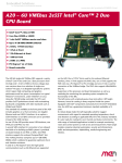
A20 – 6U VME 2eSST Intel®
Core™ 2 Duo SBC
Configuration example
User Manual
®
A20 - 6U VME 2eSST Intel Core 2 Duo SBC
A20 - 6U VME 2eSST Intel Core 2 Duo SBC
The A20 6U single-slot VMEbus SBC supports a variety of Intel® Core™ Duo and
Core 2 Duo processors from the high-end 1.5 GHz L7400 to the low-voltage dualcore versions down to a selection of single-core Celeron® M types. It is designed
especially for systems which require high computing and graphics performance and
low power consumption in a typical Windows® environment, under VxWorks® or
Linux.
Using the new Tundra TSI148 bridge controller it provides 2eSST performance
levels while maintaining backwards compatibility with older standards such as
VME64 and VME32.
The standard I/O available at the front panel of the A20 includes graphics on a VGA
connector, one Gigabit Ethernet and one USB 2.0 interface. As an option a COM
interface on an RJ45 connector can be provided instead of the USB interface.
As rear I/O the A20 provides seven USB interfaces, one SATA port and PMC rear I/O.
A second SATA interface for connection of an on-board hard disk or for building up
RAID systems is provided on-board instead of one PMC or XMC. One PATA
interface supports the on-board CompactFlash® slot.
The working memory comprises up to 4 GB DDR2 DRAM which is soldered to
guarantee optimum shock and vibration resistance.
A total of six PCI Express® lanes for high-speed communication (such as Gb
Ethernet) are supported on the A20. One x1 PCIe® link is used for the on-board
Ethernet interface, three x1 links support the XMC slots, one x1 link supports the
PMC slots via a PCI Express® to PCI-X bridge and one x1 link is used for
connection of the VMEbus bridge. The PMC slots support 64bit/66MHz (PCI-X).
Supervision of the processor and board temperature as well as a watchdog for
monitoring the operating system complete the functionality of the SBC.
The A20 comes with a tailored passive heat sink within 4 HP height. However,
forced air cooling is always required inside the system.
Equipped with Intel® components exclusively from the Intel® Embedded Line, the
A20 has a guaranteed minimum standard availability of 5 years.
MEN Mikro Elektronik GmbH
20A020-00 E1 – 2008-12-08
2
Technical Data
Its robust design make the A20 especially suited for rugged environments with
regard to extended operation temperature, shock and vibration according to
applicable DIN, EN or IEC industry standards. It is also ready for coating for use in
humid and dusty environments. The wide range of industrial applications include
for example monitoring, vision and control systems as well as test and
measurement. Main target markets comprise industrial automation, security and
infotainment, traffic and transportation, shipbuilding, medical engineering and
robotics.
Technical Data
CPU
• Up to Intel® Core™ 2 Duo L7400
- Dual-core 64-bit processor
- Up to 1.5GHz processor core frequency
- Up to 667MHz front-side bus frequency
• Chipset
- Northbridge: Intel® 945GME Express
- Southbridge: Intel® ICH7-M DH
Memory
• 4MB L2 cache integrated in Core 2 Duo
• Up to 4GB SDRAM system memory
- Soldered
- DDR2
- 667MHz memory bus frequency
- Dual-channel, 2x64 bits
• CompactFlash® card interface
- Via on-board IDE
- Type I
- True IDE
- DMA support
• 8Mbits boot Flash
• Serial EEPROM 2kbits for factory settings
Mass Storage
• Parallel IDE (PATA)
- One IDE port for local CompactFlash®
• Serial ATA (SATA)
- One channel for on-board hard disk
- One channel via rear I/O connector P2
- Transfer rates up to 150MB/s
- RAID level 0/1 support
MEN Mikro Elektronik GmbH
20A020-00 E1 – 2008-12-08
3
Technical Data
Graphics
• Integrated in 945GME Express chipset
- 200/250MHz 256-bit graphics core
• VGA connector at front panel
I/O
• USB
- One USB 2.0 port via Series A connector at front panel
- Seven USB 2.0 ports via rear I/O
- UHCI implementation
- Data rates up to 480Mbits/s
• Ethernet
- One 10/100/1000Base-T Ethernet channel at front panel
- RJ45 connector at front panel
- Ethernet controller connected by one x1 PCIe® link
- On-board LEDs to signal activity status and connection speed
Front Connections
• VGA
• One USB 2.0 (Series A)
• One Ethernet (RJ45)
Rear I/O
• USB 2.0, seven ports
• PMC rear I/O (for one PMC)
• One SATA channel
Mezzanine Slot
• Two slots usable for PMC or XMC
• XMC slots
- Compliant with XMC standard VITA 42.3-2006
- Two x1 PCI Express® links for slot 2
- One x1 PCI Express® link for slot 1
• PMC slots
- Compliant with PMC standard IEEE 1386.1
- PCI / PCI-X 32/64 bit, 33/66MHz, 3.3V V(I/O)
- One x1 PCI Express® link via PCI Express® to PCI-X bridge
- PMC I/O module (PIM) support (for one PMC)
- Current limited to 2A for 5V and 3.3V
MEN Mikro Elektronik GmbH
20A020-00 E1 – 2008-12-08
4
Technical Data
Miscellaneous
•
•
•
•
•
•
Board controller
Real-time clock, buffered by a GoldCap and a battery
Watchdog timer
Temperature measurement
One user LED
Reset button
PCI Express®
•
•
•
•
One x1 link to connect local 1000Base-T Ethernet controller
Three x1 links to connect XMC
One x1 link to connect PMC via PCI Express® to PCI-X bridge
One x1 link to connect the Tundra VME bridge via a PCI Express® to PCI-X
bridge
• Data rate up to 250MB/s in each direction (2.5 Gbits/s per lane)
VMEbus
•
•
•
•
•
•
•
•
•
•
•
•
•
•
•
Tundra TSI148 controller
Compliant with VME64 Specification
Supports VME32, VME64, 2eVME and 2eSST (VITA 1.5)
Maximum data rate 250 MB/s (limited by PCI Express® link)
Slot-1 function with auto-detection
Master
- D08:D16:D32:D64:A16:A24:A32:A64:BLT:MBLT:RMW
Slave
- D08:D16:D32:D64:A16:A24:A32:A64:BLT:MBLT
DMA
Mailbox functionality
Bus timer
Location Monitor
Interrupter D08(O):I(7-1):ROAK
Interrupt handler D08(O):IH(7-1)
Single level 3 fair requester
Single level 3 arbiter
Electrical Specifications
• Supply voltage/power consumption:
- +5V (-3%/+5%), 3.2A (idle)..6.6A (full load)
- 3.3V for XMC/PMC are generated on-board
Mechanical Specifications
• Dimensions: standard double Eurocard, 233.3mm x 160mm
• Front panel: 4HP with ejector
• Weight:
- Without XMC/PMC: 525g
MEN Mikro Elektronik GmbH
20A020-00 E1 – 2008-12-08
5
Technical Data
Environmental Specifications
• Temperature range (operation):
- 0..+60°C
- Airflow: min. 1.5m/s
• Temperature range (storage): -40..+85°C
• Relative humidity (operation): max. 95% non-condensing
• Relative humidity (storage): max. 95% non-condensing
• Altitude: -300m to + 3,000m
• Shock: 15g/11ms (EN 60068-2-27)
• Bump: 10g/16ms (EN 60068-2-29)
• Vibration (sinusoidal): 1g/ 10..150Hz (EN 60068-2-6)
• Conformal coating on request
MTBF
• tbd @ 40°C according to IEC/TR 62380 (RDF2000)
Safety
• PCB manufactured with a flammability rating of 94V-0 by UL recognized manufacturers
EMC
• Tested according to EN 55022 Class A (radio disturbance), EN 61000-4-2
(ESD), EN 61000-4-4 (burst) and EN 61000-4-5 (surge)
BIOS
• Award BIOS
Software Support
•
•
•
•
•
Windows®
Linux
VxWorks®
QNX® (on request)
Intel® Virtualization Technology, allows a platform to run multiple operating
systems and applications in independent partitions; one computer system can
function as multiple "virtual" systems
• For more information on supported operating system versions and drivers see
online data sheet.
MEN Mikro Elektronik GmbH
20A020-00 E1 – 2008-12-08
6
Block Diagram
Block Diagram
F
Intel®
Core™ (2) Duo
R
Front panel
connector
Rear I/O
connector
System Memory
DDR2 SDRAM
System Memory
DDR2 SDRAM
945GME Express
Memory Controller
Graphics Controller
VGA
F
Watchdog
IDE (PATA)
CompactFlash®
IDE (SATA)
On-board Hard
Disk
R
PCIe x1
ICH7-M DH
USB 2.0
F
USB 2.0
R
USB 2.0
R
USB 2.0
R
USB 2.0
R
USB 2.0
R
USB 2.0
R
USB 2.0
R
Ethernet
10/100/1000Base-T
SPI
F
Boot Flash
I/O Controller Hub
PCIe x1
PCIe x1
Shared slot
XMC or
F
PMC
PCI-X
PCIe x1
PCI Express
to PCI Bridge
Shared slot
PMC or
SPI
PCIe x1
R
F
XMC
PCIe x1
Boot Flash
PCI Express
to PCI Bridge
PCI-X
VME
P1
PCI-toVMEbus
Bridge
VMEbus
VME
P2
R
MEN Mikro Elektronik GmbH
20A020-00 E1 – 2008-12-08
7
Configuration Options
Configuration Options
CPU
•
•
•
•
Core 2 Duo L7400, 1.5GHz LV
Core Duo L2400, 1.66GHz LV
Core Duo U2500, 1.2GHz ULV
Celeron® M 423, 1.06 GHz
Memory
• System RAM
- 512 MB, 1 GB, 2 GB or 4 GB
• CompactFlash®
- 0 MB up to maximum available
I/O
• UART (instead of front USB and one PCI Express link)
- One RJ45 connector at front panel
- Data rates 300bit/s..230kbit/s
- FIFO receive and transmit buffers for high data throughput
- Handshake lines: full support
Please note that some of these options may only be available for large volumes.
Please ask our sales staff for more information.
For available standard configurations see online data sheet.
MEN Mikro Elektronik GmbH
20A020-00 E1 – 2008-12-08
8
Product Safety
Product Safety
!
Lithium Battery
This board contains a lithium battery. There is a danger of explosion if the
battery is incorrectly replaced!
See Chapter 5 Maintenance on page 79.
!
Electrostatic Discharge (ESD)
Computer boards and components contain electrostatic sensitive devices.
Electrostatic discharge (ESD) can damage components. To protect the board and
other components against damage from static electricity, you should follow some
precautions whenever you work on your computer.
• Power down and unplug your computer system when working on the inside.
• Hold components by the edges and try not to touch the IC chips, leads, or circuitry.
• Use a grounded wrist strap before handling computer components.
• Place components on a grounded antistatic pad or on the bag that came with the
component whenever the components are separated from the system.
• Store the board only in its original ESD-protected packaging. Retain the original
packaging in case you need to return the board to MEN for repair.
MEN Mikro Elektronik GmbH
20A020-00 E1 – 2008-12-08
9
About this Document
About this Document
This user manual describes the hardware functions of the board, connection of
peripheral devices and integration into a system. It also provides additional
information for special applications and configurations of the board.
The manual does not include detailed information on individual components (data
sheets etc.). A list of literature is given in the appendix.
History
Issue
E1
Comments
First issue
Date of Issue
2008-12-08
Conventions
!
italics
bold
monospace
hyperlink
This sign marks important notes or warnings concerning proper functionality of the
product described in this document. You should read them in any case.
Folder, file and function names are printed in italics.
Bold type is used for emphasis.
A monospaced font type is used for hexadecimal numbers, listings, C function
descriptions or wherever appropriate. Hexadecimal numbers are preceded by "0x".
Hyperlinks are printed in blue color.
The globe will show you where hyperlinks lead directly to the Internet, so you can
look for the latest information online.
IRQ#
/IRQ
Signal names followed by "#" or preceded by a slash ("/") indicate that this signal is
either active low or that it becomes active at a falling edge.
in/out
Signal directions in signal mnemonics tables generally refer to the corresponding
board or component, "in" meaning "to the board or component", "out" meaning
"coming from it".
MEN Mikro Elektronik GmbH
20A020-00 E1 – 2008-12-08
10
About this Document
Legal Information
MEN Mikro Elektronik reserves the right to make changes without further notice to any products herein. MEN makes no
warranty, representation or guarantee regarding the suitability of its products for any particular purpose, nor does MEN assume
any liability arising out of the application or use of any product or circuit, and specifically disclaims any and all liability,
including without limitation consequential or incidental damages.
"Typical" parameters can and do vary in different applications. All operating parameters, including "Typicals" must be
validated for each customer application by customer's technical experts.
MEN does not convey any license under its patent rights nor the rights of others.
Unless agreed otherwise, MEN products are not designed, intended, or authorized for use as components in systems intended
for surgical implant into the body, or other applications intended to support or sustain life, or for any other application in which
the failure of the MEN product could create a situation where personal injury or death may occur. Should Buyer purchase or
use MEN products for any such unintended or unauthorized application, Buyer shall indemnify and hold MEN and its officers,
employees, subsidiaries, affiliates, and distributors harmless against all claims, costs, damages, and expenses, and reasonable
attorney fees arising out of, directly or indirectly, any claim of personal injury or death associated with such unintended or
unauthorized use, even if such claim alleges that MEN was negligent regarding the design or manufacture of the part.
Unless agreed otherwise, the products of MEN Mikro Elektronik are not suited for use in nuclear reactors or for application in
medical appliances used for therapeutical purposes. Application of MEN products in such plants is only possible after the user
has precisely specified the operation environment and after MEN Mikro Elektronik has consequently adapted and released the
product.
ESM™, ESMini™, MDIS™, MDIS4™, MENMON™, M-Module™, M-Modules™, SA-Adapter™, SA-Adapters™,
UBox™, USM™ and the MBIOS logo are trademarks of MEN Mikro Elektronik GmbH. PC-MIP® is a registered trademark
of MEN Micro, Inc. and SBS Technologies, Inc. MEN Mikro Elektronik®, ESMexpress® and the MEN logo are registered
trademarks of MEN Mikro Elektronik GmbH.
Intel® Atom™ and Intel® Core™ are trademarks of Intel, Inc. Celeron®, Intel®, Pentium® and Xeon® are registered
trademarks of Intel, Inc. Microsoft® and Windows® are registered trademarks of Microsoft Corp. Windows® Vista™ is a
trademark of Microsoft Corp. PCI Express® and PCIe® are registered trademarks of PCI-SIG. PXI™ is a trademark of
National Instruments Corp. QNX® is a registered trademark of QNX Ltd. CompactFlash® is a registered trademark of
SanDisk Corp. Tornado® and VxWorks® are registered trademarks of Wind River Systems, Inc.
All other products or services mentioned in this publication are identified by the trademarks, service marks, or product names
as designated by the companies who market those products. The trademarks and registered trademarks are held by the
companies producing them. Inquiries concerning such trademarks should be made directly to those companies. All other brand
or product names are trademarks or registered trademarks of their respective holders.
Information in this document has been carefully checked and is believed to be accurate as of the date of publication; however,
no responsibility is assumed for inaccuracies. MEN Mikro Elektronik accepts no liability for consequential or incidental
damages arising from the use of its products and reserves the right to make changes on the products herein without notice to
improve reliability, function or design. MEN Mikro Elektronik does not assume any liability arising out of the application or
use of the products described in this document.
Copyright © 2008 MEN Mikro Elektronik GmbH. All rights reserved.
Please recycle
Germany
MEN Mikro Elektronik GmbH
Neuwieder Straße 5-7
90411 Nuremberg
Phone +49-911-99 33 5-0
Fax +49-911-99 33 5-901
E-mail [email protected]
www.men.de
MEN Mikro Elektronik GmbH
20A020-00 E1 – 2008-12-08
France
MEN Mikro Elektronik SA
18, rue René Cassin
ZA de la Châtelaine
74240 Gaillard
Phone +33 (0) 450-955-312
Fax +33 (0) 450-955-211
E-mail [email protected]
www.men-france.fr
USA
MEN Micro, Inc.
24 North Main Street
Ambler, PA 19002
Phone (215) 542-9575
Fax (215) 542-9577
E-mail [email protected]
www.menmicro.com
11
Contents
Contents
1 Getting Started . . . . . . . . . . . . . . . . . . . . . . . . . . . . . . . . . . . . . . . . . . . . . . . .
1.1 Map of the Board. . . . . . . . . . . . . . . . . . . . . . . . . . . . . . . . . . . . . . . . .
1.2 Configuring the Hardware . . . . . . . . . . . . . . . . . . . . . . . . . . . . . . . . . .
1.3 Integrating the Board into a System . . . . . . . . . . . . . . . . . . . . . . . . . .
1.4 Troubleshooting at Start-up . . . . . . . . . . . . . . . . . . . . . . . . . . . . . . . . .
1.5 Configuring BIOS . . . . . . . . . . . . . . . . . . . . . . . . . . . . . . . . . . . . . . . .
1.6 Installing Operating System Software. . . . . . . . . . . . . . . . . . . . . . . . .
1.6.1
Installing Windows 2000 via USB . . . . . . . . . . . . . . . . . . . .
1.7 Installing Driver Software . . . . . . . . . . . . . . . . . . . . . . . . . . . . . . . . . .
16
16
17
18
19
19
19
19
19
2 Functional Description . . . . . . . . . . . . . . . . . . . . . . . . . . . . . . . . . . . . . . . . . .
2.1 Power Supply. . . . . . . . . . . . . . . . . . . . . . . . . . . . . . . . . . . . . . . . . . . .
2.2 Board Supervision . . . . . . . . . . . . . . . . . . . . . . . . . . . . . . . . . . . . . . . .
2.3 Reset and Power-Off Behavior . . . . . . . . . . . . . . . . . . . . . . . . . . . . . .
2.4 Real-Time Clock . . . . . . . . . . . . . . . . . . . . . . . . . . . . . . . . . . . . . . . . .
2.5 Processor Core. . . . . . . . . . . . . . . . . . . . . . . . . . . . . . . . . . . . . . . . . . .
2.5.1
Thermal Considerations . . . . . . . . . . . . . . . . . . . . . . . . . . . .
2.6 Bus Structure . . . . . . . . . . . . . . . . . . . . . . . . . . . . . . . . . . . . . . . . . . . .
2.7 Memory . . . . . . . . . . . . . . . . . . . . . . . . . . . . . . . . . . . . . . . . . . . . . . . .
2.7.1
DRAM System Memory . . . . . . . . . . . . . . . . . . . . . . . . . . . .
2.7.2
Boot Flash . . . . . . . . . . . . . . . . . . . . . . . . . . . . . . . . . . . . . . .
2.7.3
EEPROM. . . . . . . . . . . . . . . . . . . . . . . . . . . . . . . . . . . . . . . .
2.8 Mass Storage . . . . . . . . . . . . . . . . . . . . . . . . . . . . . . . . . . . . . . . . . . . .
2.8.1
Parallel IDE (PATA) . . . . . . . . . . . . . . . . . . . . . . . . . . . . . . .
2.8.2
Serial ATA (SATA) . . . . . . . . . . . . . . . . . . . . . . . . . . . . . . . .
2.9 Graphics. . . . . . . . . . . . . . . . . . . . . . . . . . . . . . . . . . . . . . . . . . . . . . . .
2.9.1
Connection via VGA. . . . . . . . . . . . . . . . . . . . . . . . . . . . . . .
2.10 USB Interfaces. . . . . . . . . . . . . . . . . . . . . . . . . . . . . . . . . . . . . . . . . . .
2.10.1 Front-Panel Connection . . . . . . . . . . . . . . . . . . . . . . . . . . . .
2.10.2 Rear I/O Connection . . . . . . . . . . . . . . . . . . . . . . . . . . . . . . .
2.11 Ethernet Interfaces. . . . . . . . . . . . . . . . . . . . . . . . . . . . . . . . . . . . . . . .
2.11.1 Front Connection. . . . . . . . . . . . . . . . . . . . . . . . . . . . . . . . . .
2.12 UART Interface (Option). . . . . . . . . . . . . . . . . . . . . . . . . . . . . . . . . . .
2.13 XMC Slots . . . . . . . . . . . . . . . . . . . . . . . . . . . . . . . . . . . . . . . . . . . . . .
2.13.1 Connection . . . . . . . . . . . . . . . . . . . . . . . . . . . . . . . . . . . . . .
2.13.2 Installing an XMC Mezzanine Module. . . . . . . . . . . . . . . . .
2.14 PMC Slots . . . . . . . . . . . . . . . . . . . . . . . . . . . . . . . . . . . . . . . . . . . . . .
2.14.1 Installing a PMC Mezzanine Module . . . . . . . . . . . . . . . . . .
2.15 PCI Express . . . . . . . . . . . . . . . . . . . . . . . . . . . . . . . . . . . . . . . . . . . . .
2.15.1 General . . . . . . . . . . . . . . . . . . . . . . . . . . . . . . . . . . . . . . . . .
2.15.2 Implementation on the A20. . . . . . . . . . . . . . . . . . . . . . . . . .
2.16 VMEbus Interface . . . . . . . . . . . . . . . . . . . . . . . . . . . . . . . . . . . . . . . .
20
20
20
21
21
22
22
22
23
23
23
23
24
24
28
31
31
32
32
32
33
33
34
35
35
40
41
42
43
43
43
44
MEN Mikro Elektronik GmbH
20A020-00 E1 – 2008-12-08
12
Contents
2.16.1 General . . . . . . . . . . . . . . . . . . . . . . . . . . . . . . . . . . . . . . . . . 44
2.16.2 Connection . . . . . . . . . . . . . . . . . . . . . . . . . . . . . . . . . . . . . . 45
2.17 Reset Button and Status LED . . . . . . . . . . . . . . . . . . . . . . . . . . . . . . . 50
3 BIOS . . . . . . . . . . . . . . . . . . . . . . . . . . . . . . . . . . . . . . . . . . . . . . . . . . . . . . . . .
3.1 Main Menu . . . . . . . . . . . . . . . . . . . . . . . . . . . . . . . . . . . . . . . . . . . . .
3.2 Standard CMOS Features . . . . . . . . . . . . . . . . . . . . . . . . . . . . . . . . . .
3.3 Advanced BIOS Features . . . . . . . . . . . . . . . . . . . . . . . . . . . . . . . . . .
3.4 Advanced Chipset Features . . . . . . . . . . . . . . . . . . . . . . . . . . . . . . . . .
3.5 Integrated Peripherals . . . . . . . . . . . . . . . . . . . . . . . . . . . . . . . . . . . . .
3.6 Special Features. . . . . . . . . . . . . . . . . . . . . . . . . . . . . . . . . . . . . . . . . .
3.7 Power Management Setup . . . . . . . . . . . . . . . . . . . . . . . . . . . . . . . . . .
3.8 PNP/PCI Configurations . . . . . . . . . . . . . . . . . . . . . . . . . . . . . . . . . . .
3.9 PC Health Status . . . . . . . . . . . . . . . . . . . . . . . . . . . . . . . . . . . . . . . . .
3.10 Frequency/Voltage Control . . . . . . . . . . . . . . . . . . . . . . . . . . . . . . . . .
3.11 Load BIOS Default Values . . . . . . . . . . . . . . . . . . . . . . . . . . . . . . . . .
3.12 Load Last Saved Values. . . . . . . . . . . . . . . . . . . . . . . . . . . . . . . . . . . .
3.13 Set Password . . . . . . . . . . . . . . . . . . . . . . . . . . . . . . . . . . . . . . . . . . . .
3.14 Save & Exit Setup . . . . . . . . . . . . . . . . . . . . . . . . . . . . . . . . . . . . . . . .
3.15 Exit without Saving . . . . . . . . . . . . . . . . . . . . . . . . . . . . . . . . . . . . . . .
51
51
52
54
58
61
64
65
69
72
72
73
73
73
73
73
4 Organization of the Board . . . . . . . . . . . . . . . . . . . . . . . . . . . . . . . . . . . . . . .
4.1 Memory Mappings . . . . . . . . . . . . . . . . . . . . . . . . . . . . . . . . . . . . . . .
4.1.1
Processor View of the Memory Map. . . . . . . . . . . . . . . . . . .
4.1.2
I/O Memory Map . . . . . . . . . . . . . . . . . . . . . . . . . . . . . . . . .
4.2 PCI Devices . . . . . . . . . . . . . . . . . . . . . . . . . . . . . . . . . . . . . . . . . . . . .
4.3 SMBus Devices . . . . . . . . . . . . . . . . . . . . . . . . . . . . . . . . . . . . . . . . . .
4.4 Interrupt Handling . . . . . . . . . . . . . . . . . . . . . . . . . . . . . . . . . . . . . . . .
74
74
74
75
76
77
78
5 Maintenance . . . . . . . . . . . . . . . . . . . . . . . . . . . . . . . . . . . . . . . . . . . . . . . . . . 79
5.1 Lithium Battery . . . . . . . . . . . . . . . . . . . . . . . . . . . . . . . . . . . . . . . . . . 79
6 Appendix . . . . . . . . . . . . . . . . . . . . . . . . . . . . . . . . . . . . . . . . . . . . . . . . . . . . . 80
6.1 Literature and Web Resources . . . . . . . . . . . . . . . . . . . . . . . . . . . . . . . 80
6.1.1
CPU . . . . . . . . . . . . . . . . . . . . . . . . . . . . . . . . . . . . . . . . . . . . 80
6.1.2
IDE . . . . . . . . . . . . . . . . . . . . . . . . . . . . . . . . . . . . . . . . . . . . 80
6.1.3
SATA . . . . . . . . . . . . . . . . . . . . . . . . . . . . . . . . . . . . . . . . . . . 80
6.1.4
USB . . . . . . . . . . . . . . . . . . . . . . . . . . . . . . . . . . . . . . . . . . . . 80
6.1.5
Ethernet . . . . . . . . . . . . . . . . . . . . . . . . . . . . . . . . . . . . . . . . . 81
6.1.6
XMC/PMC . . . . . . . . . . . . . . . . . . . . . . . . . . . . . . . . . . . . . . 82
6.1.7
PCI Express. . . . . . . . . . . . . . . . . . . . . . . . . . . . . . . . . . . . . . 82
6.1.8
VMEbus . . . . . . . . . . . . . . . . . . . . . . . . . . . . . . . . . . . . . . . . 82
6.2 Finding out the Board’s Article Number, Revision and Serial Number83
MEN Mikro Elektronik GmbH
20A020-00 E1 – 2008-12-08
13
Figures
Figure 1.
Figure 2.
Figure 3.
Figure 4.
Figure 5.
MEN Mikro Elektronik GmbH
20A020-00 E1 – 2008-12-08
Map of the board – front panel and top view . . . . . . . . . . . . . . . . . . . .
Installing an XMC mezzanine module . . . . . . . . . . . . . . . . . . . . . . . . .
Installing a PMC mezzanine module . . . . . . . . . . . . . . . . . . . . . . . . . .
Position of battery on the A20 . . . . . . . . . . . . . . . . . . . . . . . . . . . . . . .
Labels giving the board’s article number, revision and serial number.
16
40
42
79
83
14
Tables
Table 1.
Table 2.
Table 3.
Table 4.
Table 5.
Table 6.
Table 7.
Table 8.
Table 9.
Table 10.
Table 11.
Table 12.
Table 13.
Table 14.
Table 15.
Table 16.
Table 17.
Table 18.
Table 19.
Table 20.
Table 21.
Table 22.
MEN Mikro Elektronik GmbH
20A020-00 E1 – 2008-12-08
Processor core options on A20 . . . . . . . . . . . . . . . . . . . . . . . . . . . . . . .
Pin assignment of 40-pin IDE PATA ZIF connector . . . . . . . . . . . . . .
Signal mnemonics of 40-pin IDE PATA connector. . . . . . . . . . . . . . .
Pin assignment of 15-pin HD-Sub VGA receptacle connector . . . . . .
Signal mnemonics of 15-pin HD-Sub VGA connector . . . . . . . . . . . .
Pin assignment of USB front-panel connectors . . . . . . . . . . . . . . . . . .
Signal mnemonics of USB front-panel connectors . . . . . . . . . . . . . . .
Signal mnemonics of Ethernet 10/100/1000Base-T connector . . . . . .
Pin assignment and status LEDs of 8-pin RJ45 Ethernet 10/100/
1000Base-T connectors (LAN1) . . . . . . . . . . . . . . . . . . . . . . . . . . . . .
Pin assignment of RS232 connector. . . . . . . . . . . . . . . . . . . . . . . . . . .
Signal mnemonics of UART interface . . . . . . . . . . . . . . . . . . . . . . . . .
Pin assignment of 114-pin XMC connector J15 (slot 1) . . . . . . . . . . .
Pin assignment of 114-pin XMC connector J25 (slot 2) . . . . . . . . . . .
Pin assignment of 114-pin XMC connector J26. . . . . . . . . . . . . . . . . .
Signal mnemonics of 114-pin XMC connector . . . . . . . . . . . . . . . . . .
Pin assignment of VME64 bus connector P1 . . . . . . . . . . . . . . . . . . . .
Pin assignment of VMEbus rear I/O connector P2 (PMC signals) . . .
Signal mnemonics of VMEbus rear I/O connector P2 . . . . . . . . . . . . .
Memory map – processor view . . . . . . . . . . . . . . . . . . . . . . . . . . . . . .
Memory map – I/O . . . . . . . . . . . . . . . . . . . . . . . . . . . . . . . . . . . . . . . .
PCI devices . . . . . . . . . . . . . . . . . . . . . . . . . . . . . . . . . . . . . . . . . . . . . .
SMBus devices . . . . . . . . . . . . . . . . . . . . . . . . . . . . . . . . . . . . . . . . . . .
22
25
26
31
31
32
32
33
33
34
34
36
37
38
39
46
48
49
74
75
76
77
15
Getting Started
1
Getting Started
This chapter gives an overview of the board and some hints for first installation in a
system.
1.1
Map of the Board
Figure 1. Map of the board – front panel and top view
PMC/XMC 2
VMEbus P1
Battery Holder
XMC/PMC 2
SATA Connector
PMC/XMC 1
XMC/PMC 1
USB
Ethernet
VMEbus P2
USB
Ethernet
Heat Sink
VGA
MEN Mikro Elektronik GmbH
20A020-00 E1 – 2008-12-08
VGA
Compact Flash
Holder
16
Getting Started
1.2
Configuring the Hardware
You should check your hardware requirements before installing the board in a
system, since most modifications are difficult or even impossible to do when the
board is mounted in a system.
The following check list gives an overview on what you might want to configure.
; CompactFlash
The board is shipped without a CompactFlash card. You should check your
needs and install a suitable CompactFlash card.
Refer to Chapter 2.8.1.2 Inserting and Extracting a CompactFlash Card
on page 27 for details on the IDE interface.
; PMC or XMC
The board offers the option of connecting one or two PMCs or XMCs. It detects
automatically whether a PMC or XMC is plugged.
Refer to Chapter 2.13 XMC Slots on page 35 or Chapter 2.14 PMC Slots
on page 41 for more details on the mezzanine cards.
; SATA hard disk
The board offers the option of installing a SATA hard disk instead of one XMC/
PMC. A special mounting kit is available from MEN.
Refer to Chapter 2.8.2.1 Installing a SATA Hard Disk on page 28 for
more details.
MEN Mikro Elektronik GmbH
20A020-00 E1 – 2008-12-08
17
Getting Started
1.3
Integrating the Board into a System
You can use the following check list when installing the A20 in a system for the first
time and with minimum configuration.
; Power-down the system.
; Remove all boards from the VMEbus system.
; Insert the A20 into slot 1 of the system, making sure that the VMEbus connectors are properly aligned.
; Connect a USB keyboard and mouse to the USB connectors at the front panel.
; Connect a CRT or flat-panel display to the VGA connector at the front panel.
; Power-up the system.
; You can start up the BIOS setup menu by hitting the <DEL> key (see Chapter 3
BIOS on page 51).
; Now you can make configurations in BIOS (see Chapter 3 BIOS on page 51).
; Observe the installation instructions for the respective software.
MEN Mikro Elektronik GmbH
20A020-00 E1 – 2008-12-08
18
Getting Started
1.4
Troubleshooting at Start-up
If you have any problems at start-up of the A20, you can start the board with BIOS
default settings for troubleshooting. Please refer to Chapter 3 BIOS on page 51.
1.5
Configuring BIOS
The A20 is equipped with an industry-standard BIOS. Normally you won’t need to
make any changes in the BIOS setup. If you do, however, you find further details on
the A20’s BIOS in Chapter 3 BIOS on page 51.
1.6
Installing Operating System Software
The board supports Windows, Linux, VxWorks, and QNX.
!
By standard, no operating system is installed on the board. Please refer to the
operating system installation documentation on how to install the software!
You can find any software available on MEN’s website.
1.6.1
Installing Windows 2000 via USB
If you want to install Windows 2000 using a USB CD-ROM drive, you must install
from a Windows 2000 CD including Service Pack 4 to avoid problems. This is a
known Windows problem.
1.7
Installing Driver Software
For a detailed description on how to install driver software please refer to the
respective documentation.
You can find any driver software and documentation available for download on
MEN’s website.
MEN Mikro Elektronik GmbH
20A020-00 E1 – 2008-12-08
19
Functional Description
2
Functional Description
The following describes the individual functions of the board and their
configuration on the board. There is no detailed description of the individual
controller chips and the CPU. They can be obtained from the data sheets or data
books of the semiconductor manufacturer concerned (Chapter 6.1 Literature and
Web Resources on page 80).
2.1
Power Supply
The board is supplied via VMEbus with +5V only (3.3V is not connected to the
backplane). It is possible to power the board with 12V and -12V which may be
required by some PMC or XMC modules.
The CPU operates between 0.85V and 1.3V core voltage (depends on CPU type and
CPU load). The DDR2 SDRAM memory works with 1.8V. These voltages are
generated on the board.
The PCI I/O voltage is 3.3V.
2.2
Board Supervision
The A20 provides an intelligent board controller (BC). The BC supervises 5V and
3.3V and holds the CPU in reset condition until all supply voltages are within their
nominal values. It has the following main features:
•
•
•
•
•
•
System watchdog
Software reset
Voltage monitoring
Emergency temperature shutdown at 125°C processor die temperature
Error state logging
SMBus interface
The watchdog device monitors the board on operating system level. If enabled, the
watchdog must be triggered by application software. If the trigger is overdue, the
watchdog initiates a board reset and this way can put the system back into operation
when the software hangs.
The watchdog uses a configurable time interval or is disabled. Settings are made
through BIOS or via an MEN software driver. See also Chapter Onboard Device —
Sub-menu on page 63.
In addition, an LM63 supervision device is implemented for thermal monitoring. It
checks the processor die temperature and the board temperature.
MEN provides dedicated software drivers for the board controller and LM63 device.
For a detailed description of the functionality of the driver software please refer to
the drivers’ documentation.
You can find any driver software and documentation available for download on
MEN’s website.
MEN Mikro Elektronik GmbH
20A020-00 E1 – 2008-12-08
20
Functional Description
2.3
Reset and Power-Off Behavior
The A20 generates its own reset signal. You can wake it up from reset state by
externally switching the power supply off and on.
When turning on the power supply the BIOS generates one of these states: Off
(=Reset), On or Former State. The executed event depends on the BIOS setting. The
VME bridge (if it receives a reset signal from the VMEbus) and the recessed button
on the front panel generate a board reset signal.
2.4
Real-Time Clock
The board includes a real-time clock connected to the Southbridge. For data
retention during power off the RTC is backed up by a GoldCap capacitor. The
GoldCap gives an autonomy of approx. 14 hours when fully loaded. Under normal
conditions, replacement should be superfluous during lifetime of the board. The
RTC can generate interrupt requests to the Southbridge.
For retention of time/date data after a power off of more than 8-10 hours the RTC is
also backed by a battery.
Please contact MEN’s sales team for further information.
MEN Mikro Elektronik GmbH
20A020-00 E1 – 2008-12-08
21
Functional Description
2.5
Processor Core
The A20 is equipped with an Intel Core Duo, Core 2 Duo or single-core Celeron M
processor core. The following table gives a performance overview:
Table 1. Processor core options on A20
Processor Type Core Frequency Power Class1 L2 Cache Front Side Bus
Core 2 Duo
L7400
17 W
4 MB
667 MHz
Core Duo L2400 1.66 GHz
15 W (LV)
2 MB
667 MHz
Core Duo U2500 1.2 GHz
9 W (ULV)
2 MB
533 MHz
Celeron M 423
5.5 W (ULV)
1 MB
533 MHz
1
1.5 GHz
1.07 GHz
ULV = Ultra Low Voltage
LV = Low Voltage
2.5.1
Thermal Considerations
A suitable heat sink is provided to meet thermal requirements. For special
requirements a larger heat sink is also available on request. Please contact MEN
sales for more information.
!
Please note that if you use any other heat sink than that supplied by MEN, or no heat
sink at all, warranty on functionality and reliability of the A20 may cease. If you
have any questions or problems regarding thermal behavior, please contact MEN.
2.6
Bus Structure
The A20 uses an Intel 945GME Express component as the Northbridge1 that
connects to the processor core and controls memory and graphics, and an Intel ICH7M DH I/O Controller Hub as the Southbridge2. Any I/O is directly controlled by this
chipset, there is no local PCI bus.
The board has a standard Tundra TSI148 PCI-to-VME bridge for connection to the
VMEbus. The bridge uses one PCI Express link from the Southbridge via a PCI
Express-to-PCI-bridge.
1
The Northbridge is the component of the chip set that is located closely to the CPU, for
fast data transfer.
2 The Southbridge is the component of the chip set that connects to PCI devices and controls
data exchange with peripherals and other interfaces.
MEN Mikro Elektronik GmbH
20A020-00 E1 – 2008-12-08
22
Functional Description
2.7
Memory
The standard board versions provide a memory configuration suitable for many
applications. However, memory on the A20 can also be configured for your needs.
For standard memory sizes and ordering options please see MEN’s website.
2.7.1
DRAM System Memory
The board provides up to 4 GB on-board, soldered DDR2 (double data rate)
SDRAM. The memory bus is 2x64 bits wide (dual channel) and operates at
667 MHz.
2.7.2
Boot Flash
The A20 has an 8-Mbit SPI Serial Flash implemented as on-board Flash for BIOS
data.
2.7.3
EEPROM
The board has a 2-kbit serial EEPROM for factory data.
MEN Mikro Elektronik GmbH
20A020-00 E1 – 2008-12-08
23
Functional Description
2.8
Mass Storage
2.8.1
Parallel IDE (PATA)
The parallel IDE (PATA) interface is controlled by the Southbridge and provides one
ATA channel with master and slave support. Devices can be operated in PIO mode 0
up to UDMA mode 5 (UDMA100).
The A20 provides an on-board CompactFlash slot. You can connect one device to a
40-pin ZIF connector.
By standard, a CompactFlash slot is assembled using a small adapter card in the
heat sink area. The slot is ready-to-use, with the ZIF connection already in place.
Even with CompactFlash the board needs only one slot in the system.
Please see MEN’s website for ordering options.
2.8.1.1
Connection
The 40-pin PATA connector is located at the top side of A20.
Connector types:
• 40-pin ZIF receptacle, 0.5mm pitch, for ribbon-cable connection
MEN Mikro Elektronik GmbH
20A020-00 E1 – 2008-12-08
24
Functional Description
Table 2. Pin assignment of 40-pin IDE PATA ZIF connector
1
40
MEN Mikro Elektronik GmbH
20A020-00 E1 – 2008-12-08
1
2
3
4
5
6
7
8
9
10
11
12
13
14
15
16
17
18
19
20
21
22
23
24
25
26
27
28
29
30
31
32
33
34
35
36
37
38
39
40
BAT_D_R
IDE_RST#
GND
IDE_D[7]
IDE_D[8]
IDE_D[6]
IDE_D[9]
IDE_D[5]
IDE_D[10]
IDE_D[4]
IDE_D[11]
IDE_D[3]
IDE_D[12]
IDE_D[2]
IDE_D[13]
IDE_D[1]
IDE_D[14]
IDE_D[0]
IDE_D[15]
GND
IDE_DRQ
GND
IDE_WR#
IDE_RD#
GND
IDE_RDY
GND
IDE_DAK#
IDE_IRQ
IDE_A[1]
IDE_A[0]
IDE_A[2]
IDE_CS1#
IDE_CS3#
+3.3V
+3.3V
-
25
Functional Description
Table 3. Signal mnemonics of 40-pin IDE PATA connector
Signal
Function
+3.3V
out
+3.3 V power supply, current-limited to 2 A by a
fuse1
GND
-
Digital ground
BAT_D_R
in
Battery for retention of RTC data (not used)
IDE_A[2:0]
out
IDE address [2:0]
IDE_CS1#
out
IDE chip select 1
IDE_CS3
out
IDE chip select 3
IDE_D[15:0]
in/out
IDE data [15:0]
IDE_DAK#
out
IDE DMA acknowledge
IDE_DRQ
in
IDE DMA request
IDE_IRQ
in
IDE interrupt request
IDE_RD#
out
IDE read strobe
IDE_RDY
in
IDE ready
IDE_RST#
out
IDE reset
IDE_WR#
out
IDE write strobe
1
The IDE fuse used on A20 is a PolyFuse and therefore needs no maintenance.
MEN Mikro Elektronik GmbH
20A020-00 E1 – 2008-12-08
Direction
26
Functional Description
2.8.1.2
Inserting and Extracting a CompactFlash Card
The A20 supports standard CompactFlash cards. For CompactFlash cards available
from MEN see MEN’s website.
The A20 is shipped without a CompactFlash card installed. To install
CompactFlash, please stick to the following procedure.
; Power down your system and remove the A20 from the system.
; Put the board on a flat surface.
VMEb
; Lift the CompactFlash holding bracket.
Heat Sink
VGA
Compact Flash
Holder
; Insert the CompactFlash card carefully as indicated by the arrow on top of the
card.
; Make sure that all the contacts are aligned properly and the card is firmly connected with the card connector.
; Push the CompactFlash holding bracket back down until it clicks into place.
; Observe manufacturer notes on usage of CompactFlash cards.
MEN Mikro Elektronik GmbH
20A020-00 E1 – 2008-12-08
27
Functional Description
2.8.2
Serial ATA (SATA)
The serial ATA (SATA) interface is controlled by the Southbridge and provides two
ATA channels. One channel can be used to connect an on-board hard disk. The other
channel is led to the VMEbus connectors for rear I/O. See Chapter 2.16 VMEbus
Interface on page 44.
The SATA interface supports transfer rates up to 150 MB/s.
The A20 offers the possibility to connect a SATA hard disk instead of one XMC/
PMC. See Chapter 2.8.2.1 Installing a SATA Hard Disk for further information.
See Chapter 6.1.8 VMEbus on page 82 for rear I/O.
2.8.2.1
Installing a SATA Hard Disk
MEN provides a mounting kit for easy connection of a SATA hard disk. All required
screws and standoffs are included in the delivery.
See MEN’s website for ordering information.
Carry out the following steps to install a SATA hard disk on the A20:
; If the A20 is already installed in a system: Power down the system and remove
the A20.
; Remove the XMC/PMC if installed.
; Connect the SATA connector and the ribbon cable to the hard disk.
SATA connector with ribbon cable
MEN Mikro Elektronik GmbH
20A020-00 E1 – 2008-12-08
28
Functional Description
; Install the four standoffs and washers on the bottom side of the hard disk.
Standoff
Washer
; Connect the SATA connector on the hard disk to the SATA connector on the
A20. Make sure to match the pins correctly. Turn the hard disk around.
; Turn the A20 around and align the four standoffs with the mounting holes
(highlighted in red) of the A20.
MEN Mikro Elektronik GmbH
20A020-00 E1 – 2008-12-08
29
Functional Description
; Screw the hard disk to the board using the four screws (highlighted in red)
included in the delivery.
; Reinsert the board into your system.
MEN Mikro Elektronik GmbH
20A020-00 E1 – 2008-12-08
30
Functional Description
2.9
Graphics
The graphics subsystem is part of the Intel 945GME Express Northbridge and
supports a 200/250 MHz 256-bit graphics core.
2.9.1
Connection via VGA
You can connect a VGA monitor directly at the A20’s front panel. The pinout of the
15-pin HD-Sub connector is standard VGA.
Connector types:
• 15-pin HD-Sub receptacle according to DIN41652/MIL-C-24308, with thread
bolt UNC 4-40
• Mating connector:
15-pin HD-Sub plug according to DIN41652/MIL-C-24308, available for ribbon
cable (insulation piercing connection), hand-soldering connection or crimp connection
Table 4. Pin assignment of 15-pin HD-Sub VGA receptacle connector
10
15
5
11
1
6
15
SCL
10
GND
5
GND
14
VSYNC
9
-
4
-
13
HSYNC
8
GND
3
B
12
SDA
7
GND
2
G
11
-
6
GND
1
R
Table 5. Signal mnemonics of 15-pin HD-Sub VGA connector
Signal
Function
GND
-
Ground
HSYNC
out
Horizontal synchronization
R, G, B
out
Analog monitor interface (red, green, blue)
SCL
out
Monitor I²C interface
SDA
in/out
VSYNC
out
MEN Mikro Elektronik GmbH
20A020-00 E1 – 2008-12-08
Direction
Vertical synchronization
31
Functional Description
2.10
USB Interfaces
The A20 provides up to eight USB 2.0 ports controlled by the Southbridge. One
USB interface is routed to standard front-panel connectors and seven can be
accessed via rear I/O.
The USB interfaces support UHCI.
2.10.1
Front-Panel Connection
One USB interface is accessible at the front panel.
Connector types:
• 4-pin USB Series A receptacle according to Universal Serial Bus Specification
Revision 1.0
• Mating connector:
4-pin USB Series A plug according to Universal Serial Bus Specification Revision 1.0
Table 6. Pin assignment of USB front-panel connectors
1
2
3
4
1
+5V
2
USB_D-
3
USB_D+
4
GND
Table 7. Signal mnemonics of USB front-panel connectors
Signal
Direction
Function
+5V
out
+5 V power supply
GND
-
Digital ground
USB_D+, USB_D- in/out
2.10.2
USB lines, differential pair
Rear I/O Connection
Seven USB interfaces are accessible via rear I/O on VMEbus connector P2.
See Chapter 2.16 VMEbus Interface on page 44 for rear I/O pin assignments.
MEN Mikro Elektronik GmbH
20A020-00 E1 – 2008-12-08
32
Functional Description
2.11
Ethernet Interfaces
The A20 offers one Ethernet interface. It is accessible at the front panel.
The Ethernet interface is connected to the Southbridge via one x1 PCI Express
(PCIe) link. It is controlled by an Intel 82573 Ethernet controller. It supports
10 Mbits/s up to 1000 Mbits/s as well as full-duplex operation and autonegotiation.
The controller uses a part of the boot Flash to store the MAC address.
!
The unique MAC address is set at the factory and should not be changed. Any
attempt to change this address may create node or bus contention and thereby render
the board inoperable.
2.11.1
Front Connection
One standard RJ45 connector is available at the front panel. There are two status
LEDs for the channel at the front panel.
The pin assignment corresponds to the Ethernet specification IEEE802.3.
Connector types:
• Modular 8/8-pin mounting jack according to FCC68
• Mating connector:
Modular 8/8-pin plug according to FCC68
Table 8. Signal mnemonics of Ethernet 10/100/1000Base-T connector
Signal
Direction
Function
BI_Dx+/-
in/out
Differential pairs of data lines for 1000Base-T
RX+/-
in
Differential pair of receive data lines for 10/
100Base-T
TX+/-
out
Differential pair of transmit data lines for 10/
100Base-T
Table 9. Pin assignment and status LEDs of 8-pin RJ45 Ethernet 10/100/1000BaseT connectors (LAN1)
1000Base-T 10/100Base-T
Lights up when a link is
established, and blinks
whenever there is transmit
or receive activity
On: Link 100Mbits/s
Off: Link with 10Mbits/s
MEN Mikro Elektronik GmbH
20A020-00 E1 – 2008-12-08
1
1
2
8
1
BI_DA+
TX+
2
BI_DA-
TX-
3
BI_DB+
RX+
4
BI_DC+
-
5
BI_DC-
-
6
BI_DB-
RX-
7
BI_DD+
-
8
BI_DD-
-
33
Functional Description
2.12
UART Interface (Option)
As an option, the A20 can be equipped with a COM interface at the front panel
instead of the USB. It is accessible via an RJ45 connector.
A VT100 terminal can be connected to the COM interface to control the BIOS and
text-based operating systems (DOS, Linux, etc).
The terminal can be connected to the COM interface via a special RJ45 to 9-pin DSub adapter cable available from MEN. For ordering options see MEN’s website.
It is possible to use the COM interface for console redirection, i.e. to maintain the
BIOS from a remote location.
The UART interfaces support transfer rates from 300bit/s to 230kbit/s.
Connector types:
• Modular 8/8-pin mounting jack according to FCC68
• Mating connector:
Modular 8/8-pin plug according to FCC68
Table 10. Pin assignment of RS232 connector
1
1
DSR#
2
DCD#
3
DTR#
4
GND
5
RXD
6
TXD
7
CTS#
8
RTS#
8
Table 11. Signal mnemonics of UART interface
Signal
Function
CTS#
in
Clear to send
DCD#
in
Data carrier detected
DSR#
in
Data set ready
DTR#
out
Data terminal ready
GND
-
Digital ground
RTS#
out
Request to send
RXD
in
Receive data
TXD
out
Transmit data
MEN Mikro Elektronik GmbH
20A020-00 E1 – 2008-12-08
Direction
34
Functional Description
2.13
XMC Slots
The A20 board provides up to two XMC slots for extension such as high-speed
graphics, Ethernet etc.
XMC modules have the same form factor as PMC modules, however they do not use
a PCI bus but a high-speed PCI Express connection and therefore have a different
carrier board connector.
According to the XMC standard there is only one link on each XMC connector.
XMC slot 1 offers one connector (J15) with one x1 PCI Express link. XMC slot 2
provides two connectors (J25 and J26) which support one x1 PCI Express link each.
The connector layout is fully compatible to the standard for XMC.3 connectors.
(See also Chapter 6.1 Literature and Web Resources on page 80.)
It is possible to use the PCI Express interface of the XMC connectors and the PCI
interface of the PMC connectors at the same time, which makes it possible to use
hybrid PMC/XMC modules.
2.13.1
Connection
Connector types:
• 114-pin XMC receptacle connector
• Mating connector:
114-pin XMC plug connector, e. g. SAMTEC ASP105885-01
MEN Mikro Elektronik GmbH
20A020-00 E1 – 2008-12-08
35
Functional Description
Table 12. Pin assignment of 114-pin XMC connector J15 (slot 1)
A B C D E F
1
2
A
B
C
D
E
F
1
PER4p0
PER4n0
+3.3V
-
-
+5V
2
GND
GND
-
GND
GND
MRSTI#
3
-
-
+3.3V
-
-
+5V
4
GND
GND
-
GND
GND
MRSTO#
5
-
-
+3.3V
-
-
+5V
6
GND
GND
-
GND
GND
+12V
7
-
-
+3.3V
-
-
+5V
8
GND
GND
-
GND
GND
-12V
9
-
-
-
-
-
+5V
10
GND
GND
-
GND
GND
GA0
11
PET4p0
PET4n0
-
-
-
+5V
12
GND
GND
GA1
GND
GND
-
13
-
-
-
-
-
+5V
14
GND
GND
GA2
GND
GND
MSDA
15
-
-
-
-
-
+5V
16
GND
GND
MVMRO
GND
GND
MSCL
17
-
-
-
-
-
-
18
GND
GND
-
GND
GND
-
-
WAKE#
ROOT0#
-
19
19 REFCLKAp REFCLKAn
MEN Mikro Elektronik GmbH
20A020-00 E1 – 2008-12-08
36
Functional Description
Table 13. Pin assignment of 114-pin XMC connector J25 (slot 2)
A B C D E F
1
2
A
B
C
D
E
F
1
PER2p0
PER2n0
+3.3V
-
-
+5V
2
GND
GND
-
GND
GND
MRSTI#
3
-
-
+3.3V
-
-
+5V
4
GND
GND
-
GND
GND
MRSTO#
5
-
-
+3.3V
-
-
+5V
6
GND
GND
-
GND
GND
+12V
7
-
-
+3.3V
-
-
+5V
8
GND
GND
-
GND
GND
-12V
9
-
-
-
-
-
+5V
10
GND
GND
-
GND
GND
GA0
11
PET2p0
PET2n0
-
-
-
+5V
12
GND
GND
GA1
GND
GND
-
13
-
-
-
-
-
+5V
14
GND
GND
GA2
GND
GND
MSDA
15
-
-
-
-
-
+5V
16
GND
GND
MVMRO
GND
GND
MSCL
17
-
-
-
-
-
-
18
GND
GND
-
GND
GND
-
-
WAKE#
ROOT0#
-
19
19 REFCLKCp REFCLKCn
MEN Mikro Elektronik GmbH
20A020-00 E1 – 2008-12-08
37
Functional Description
Table 14. Pin assignment of 114-pin XMC connector J26
A B C D E F
1
2
A
B
C
D
E
F
1
PER3p0
PER3n0
-
-
-
-
2
GND
GND
-
GND
GND
-
3
-
-
-
-
-
-
4
GND
GND
-
GND
GND
-
5
-
-
-
-
-
-
6
GND
GND
-
GND
GND
-
7
-
-
-
-
-
-
8
GND
GND
-
GND
GND
-
9
-
-
-
-
-
-
10
GND
GND
-
GND
GND
-
11
PET3p0
PET3n0
-
-
-
-
12
GND
GND
-
GND
GND
-
13
-
-
-
-
-
-
14
GND
GND
-
GND
GND
-
15
-
-
-
-
-
-
16
GND
GND
-
GND
GND
-
17
-
-
-
-
-
-
18
GND
GND
-
GND
GND
-
-
-
-
-
19
19 REFCLKEp REFCLKEn
MEN Mikro Elektronik GmbH
20A020-00 E1 – 2008-12-08
38
Functional Description
Table 15. Signal mnemonics of 114-pin XMC connector
Signal
Power
out
+12V supply voltage
+3.3V
out
+3.3V supply voltage
+5V (VPWR)
out
+5V supply voltage
GND
-
Ground
out
PCI Express link 2, lane 0, differential
receive
in
PCI Express link 2, lane 0, differential
transmit
REFCLKEp/n
out
Differential reference clock, link 2
ROOT0#
out
Root Complex enabling
WAKE#
out
Reactivation of power rails and reference clocks
out
PCI Express link 3, lane 0, differential
receive
in
PCI Express link 3, lane 0, differential
transmit
out
Differential reference clock, link 3
out
PCI Express link 4, lane 0, differential
receive
in
PCI Express link 4, lane 0, differential
transmit
REFCLKAp/n
out
Differential reference clock, link 4
GA[0..2]
out
I2C channel select
MBIST#
in
XMC built-in self test
MRSTI#
out
XMC reset in
MRSTO#
in
XMC reset out (not used)
MSCL
out
SMBus clock
MSDA
in/out
SMBus data
MVMRO
out
XMC EEPROM write prohibit
PCI
PER3p/n[0]
Express
Link 3
PET3p/n[0]
REFCLKCp/n
PCI
PER4p/n[0]
Express
Link 4
PET4p/n[0]
MEN Mikro Elektronik GmbH
20A020-00 E1 – 2008-12-08
Function
+12V, -12V
PCI
PER2p/n[0]
Express
Link 2
PET2p/n[0]
Other
Direction
39
Functional Description
2.13.2
Installing an XMC Mezzanine Module
Perform the following steps to install an XMC module:
; Power down your system and remove the A20 from the system.
; Remove the filler panel from the board’s front XMC slot, if installed.
; The XMC module is plugged on the A20 with the component sides of the PCBs
facing each other.
; Put the XMC module’s front connector through the A20’s front slot at a 45°
angle.
; Carefully put it down, making sure that the connectors are properly aligned.
; Press the XMC module firmly onto the A20.
; Make sure that the EMC gasket around the XMC front panel is properly in its
place.
; Screw the XMC module tightly to the A20 using the two mounting standoffs
and four matching oval-head cross-recessed screws of type M2.5x6.
Figure 2. Installing an XMC mezzanine module
XMC module
Mounting
standoff
114-pin
connector
CPU board
2 M2.5x6 ovalhead crossrecessed screws
MEN Mikro Elektronik GmbH
20A020-00 E1 – 2008-12-08
2 M2.5x6 ovalhead crossrecessed screws
40
Functional Description
2.14
PMC Slots
The A20 board provides one or two PMC-X slots for extension such as graphics,
Fast Ethernet etc.
!
The signaling voltage is set to 3.3V, i. e. the CPU board has a 3.3V voltage key (see
Figure 3, Installing a PMC mezzanine module, on page 42) and can only carry PMC
mezzanines that support this keying configuration. Mezzanine cards may be
designed to accept either or both signaling voltages (3.3V/5V).
The PMC-X slots support 32/64 bit and 33/66 MHz. They are connected to a PCI
Express-to-PCI-X bridge which converts one PCI Express x1 link from the
Southbridge.
PMC slot 1 supports rear I/O via VMEbus connector P2. See Table 17, Pin
assignment of VMEbus rear I/O connector P2 (PMC signals), on page 48 for the
pinout.
The connector layout is fully compatible to the IEEE1386 specification. For
connector pinouts please refer to the specification (see Chapter 6.1 Literature and
Web Resources on page 80).
Connector types:
• 64-pin, 1-mm pitch board-to-board receptacle according to IEEE 1386
• Mating connector:
64-pin, 1-mm pitch board-to-board plug according to IEEE 1386
MEN Mikro Elektronik GmbH
20A020-00 E1 – 2008-12-08
41
Functional Description
2.14.1
Installing a PMC Mezzanine Module
Perform the following steps to install a PMC module:
; Make sure that the voltage keying of your PMC module matches the A20.
; Power down your system and remove the A20 from the system.
; Remove the filler panel from the board’s front PMC slot, if installed.
; The PMC module is plugged on the A20 with the component sides of the PCBs
facing each other.
; Put the PMC module’s front connector through the A20’s front slot at a 45°
angle.
; Carefully put it down, making sure that the connectors are properly aligned.
; Press the PMC module firmly onto the A20.
; Make sure that the EMC gasket around the PMC front panel is properly in its
place.
; Screw the PMC module tightly to the A20 using the two mounting standoffs
and four matching oval-head cross-recessed screws of type M2.5x6.
Figure 3. Installing a PMC mezzanine module
PMC module
Mounting
standoff
3.3V
voltage key
64-pin
connectors
CPU board
2 M2.5x6 ovalhead crossrecessed screws
MEN Mikro Elektronik GmbH
20A020-00 E1 – 2008-12-08
2 M2.5x6 ovalhead crossrecessed screws
42
Functional Description
2.15
PCI Express
2.15.1
General
PCI Express (PCIe) succeeds PCI and AGP and offers higher data transfer rates.
As opposed to the PCI bus, PCIe is no parallel bus but a serial point-to-point
connection. Data is transferred using so-called lanes, with each lane consisting of a
line pair for transmission and a second pair for reception. Individual components are
connected using switches.
PCIe supports full-duplex operation and uses a clock rate of 1.25 GHz DDR. This
results in a data rate of max. 250 MB/s per lane in each direction. (The standard PCI
bus with 32 bits/33 MHz only allows a maximum of 133 MB/s.)
If you use only one lane, you speak of a PCIe x1 link. You can couple several lanes
to increase the data rate, e.g. x2 with 2 lanes up to a x32 link using 32 lanes.
In terms of software, most operating systems can handle PCI Express boards just as
well as the old PCI.
2.15.2
Implementation on the A20
On the A20 the Gigabit Ethernet channel is permanently connected via one PCIe x1
link. Another three x1 links are used for the connection of the XMCs and one x1
link is available for the PMCs via a PCI Express to PCI-X bridge. The sixth x1 link
is used for connection of the Tundra PCI-to-VMEbus bridge.
MEN Mikro Elektronik GmbH
20A020-00 E1 – 2008-12-08
43
Functional Description
2.16
VMEbus Interface
2.16.1
General
The A20's VMEbus interface conforms to the VME64 specification. It uses the
Tundra TSI148 controller as a PCI-to-VMEbus bridge.
The Tundra TSI148 is currently the highest bandwidth VME bridge available,
providing PCI-X-to-VME 2eSST performance levels while maintaining backwards
compatibility with older standards.
TSI148’s decoupled architecture and proper buffer sizing allows a very large
number of simultaneous transactions to take place. TSI148 is also a full featured
master, slave and system controller which allows it to be used in any VME
application.
Main features:
•
•
•
•
•
•
•
•
•
•
•
•
•
Supports VME32, VME64, 2eVME and 2eSST (VITA 1.5)
Slot-1 function with auto-detection
Master: D08:D16:D32:D64:A16:A24:A32:A64:BLT:MBLT:RMW
Slave: D08:D16:D32:D64:A16:A24:A32:A64:BLT:MBLT
DMA
Mailbox functionality
Bus timer
Location Monitor
Interrupter D08(O):I(7-1):ROAK
Interrupt handler D08(O):IH(7-1)
Single level 3 fair requester
Single level 3 arbiter
Low power consumption
Since the Tundra TSI148 controller is a very complex component, we have not
included any details on register access etc. here. Please refer to the bridge’s
manufacturer data sheet, which is available as a PDF download from Tundra’s
website: www.tundra.com.
For more literature on the VMEbus see Chapter 6.1 Literature and Web
Resources on page 80.
MEN Mikro Elektronik GmbH
20A020-00 E1 – 2008-12-08
44
Functional Description
2.16.2
Connection
Connector types:
• 160-pin, 5-row plug, performance level according to DIN41612, part 5
• Mating connector:
160-pin, 5-row receptacle, performance level according to DIN41612, part 5
2.16.2.1 Bus Connection: VMEbus P1
The pin assignment of P1 conforms to the VME64 specification ANSI/VITA 1-1994
(R2002) and VME64 Extensions Standard ANSI/VITA 1.1-1997 (R2003).
MEN Mikro Elektronik GmbH
20A020-00 E1 – 2008-12-08
45
Functional Description
Table 16. Pin assignment of VME64 bus connector P1
DCB A Z
1
32
1
2
3
4
5
6
7
8
9
10
11
12
13
14
15
16
17
18
19
20
21
22
23
24
25
26
27
28
29
30
31
32
MEN Mikro Elektronik GmbH
20A020-00 E1 – 2008-12-08
D
GND
GAP#
GA0#
GA1#
GA2#
GA3#
GA4#
GND
-
C
D8
D9
D10
D11
D12
D13
D14
D15
GND
SYSFAIL#
BERR#
SYSRESET#
LWORD#
AM5
A23
A22
A21
A20
A19
A18
A17
A16
A15
A14
A13
A12
A11
A10
A9
A8
+12V
+5V
B
BBSY#
BCLR#
ACFAIL#
BG0IN#
BG0OUT#
BG1IN#
BG1OUT#
BG2IN#
BG2OUT#
BG3IN#
BG3OUT#
BR0#
BR1#
BR2#
BR3#
AM0
AM1
AM2
AM3
GND
GND
IRQ7#
IRQ6#
IRQ5#
IRQ4#
IRQ3#
IRQ2#
IRQ1#
+5V
A
D0
D1
D2
D3
D4
D5
D6
D7
GND
SYSCLK
GND
DS1#
DS0#
WRITE#
GND
DTACK#
GND
AS#
GND
IACK#
IACKIN#
IACKOUT#
AM4
A7
A6
A5
A4
A3
A2
A1
-12V
+5V
Z
GND
GND
GND
GND
GND
GND
GND
GND
GND
GND
GND
GND
GND
GND
GND
GND
46
Functional Description
2.16.2.2 Rear I/O using VMEbus P2
The standard version of A20 provides VME64 signals and rear I/O for the PMC as
well as seven USB interfaces and a SATA channel. The PMC I/O signals are directly
connected to connector P2.
The following table gives the pin assignment for P2.
MEN Mikro Elektronik GmbH
20A020-00 E1 – 2008-12-08
47
Functional Description
Table 17. Pin assignment of VMEbus rear I/O connector P2 (PMC signals)
DCB A Z
1
32
D
C
B
A
Z
1
USB_OC6#
PMC_1
+5V
PMC_2
-
2
USB_D[6]-#
PMC_3
GND
PMC_4
GND
3
USB_D[6]+
PMC_5
RETRY#
PMC_6
-
4
USB_OC7#
PMC_7
A24
PMC_8
GND
5
USB_D[7]-#
PMC_9
A25
PMC_10
-
6
USB_D[7]+
PMC_11
A26
PMC_12
GND
7
USB_OC4#
PMC_13
A27
PMC_14
-
8
USB_D[4]-#
PMC_15
A28
PMC_16
GND
9
USB_D[4]+
PMC_17
A29
PMC_18
-
10
USB_OC5#
PMC_19
A30
PMC_20
GND
11
USB_D[5]-#
PMC_21
A31
PMC_22
-
12
USB_D[5]+
PMC_23
GND
PMC_24
GND
13
USB_OC2#
PMC_25
+5V
PMC_26
-
14
USB_D[2]-#
PMC_27
D16
PMC_28
GND
15
USB_D[2]+
PMC_29
D17
PMC_30
-
16
USB_OC3#
PMC_31
D18
PMC_32
GND
17
USB_D[3]-#
PMC_33
D19
PMC_34
-
18
USB_D[3]+
PMC_35
D20
PMC_36
GND
19
-
PMC_37
D21
PMC_38
-
20
-
PMC_39
D22
PMC_40
GND
21
-
PMC_41
D23
PMC_42
-
22
USB_OC1#
PMC_43
GND
PMC_44
GND
23
USB_D[1]-#
PMC_45
D24
PMC_46
-
24
USB_D[1]+
PMC_47
D25
PMC_48
GND
25
-
PMC_49
D26
PMC_50
-
26
SATA0_TX-
PMC_51
D27
PMC_52
GND
27
SATA0_TX+
PMC_53
D28
PMC_54
-
28
SATA0_LED
PMC_55
D29
PMC_56
GND
29
SATA0_RX-
PMC_57
D30
PMC_58
-
30
SATA0_RX+
PMC_59
D31
PMC_60
GND
31
GND
PMC_61
GND
PMC_62
-
32
-
PMC_63
+5V
PMC_64
GND
MEN Mikro Elektronik GmbH
20A020-00 E1 – 2008-12-08
48
Functional Description
Table 18. Signal mnemonics of VMEbus rear I/O connector P2
Signal
Power
IDE
SATA
VME64
USB
PMC
MEN Mikro Elektronik GmbH
20A020-00 E1 – 2008-12-08
Direction
Function
+5V
-
+5V power supply
GND
-
Digital ground
SATA0_RX+,
SATA0_RX-
in
Differential pair of SATA receive lines,
port 0
SATA0_TX+,
SATA0_TX-
out
Differential pair of SATA transmit lines,
port 0
SATA_LED#
out
SATA activity
A[31:24]
in/out
VME64 address lines
D[31:16]
in/out
VME64 data lines
RETRY#
out
VME64 retry for postponed data transfer
USB_D[1]+,
USB_D[1]-
in/out
Differential pair of USB lines, port 1
USB_D[2]+,
USB_D[2]-
in/out
Differential pair of USB lines, port 2
USB_D[3]+,
USB_D[3]-
in/out
Differential pair of USB lines, port 3
USB_D[4]+,
USB_D[4]-
in/out
Differential pair of USB lines, port 4
USB_D[5]+,
USB_D[5]-
in/out
Differential pair of USB lines, port 5
USB_D[6]+,
USB_D[6]-
in/out
Differential pair of USB lines, port 6
USB_D[7]+,
USB_D[7]-
in/out
Differential pair of USB lines, port 7
USB_OC1
in
USB overcurrent, port 1
USB_OC2
in
USB overcurrent, port 2
USB_OC3
in
USB overcurrent, port 3
USB_OC4
in
USB overcurrent, port 4
USB_OC5
in
USB overcurrent, port 5
USB_OC6
in
USB overcurrent, port 6
USB_OC7
in
USB overcurrent, port 7
PMC_xx
in/out
Signal xx from PMC rear I/O connector
J14
49
Functional Description
2.17
Reset Button and Status LED
The A20 has a reset button and one status LED at the front panel. The reset button is
recessed within the front panel and requires a tool, e.g. paper clip to be pressed,
preventing the button from being inadvertently activated.
The yellow status LED shows board status messages. The LED is controlled by a
GPIO pin of the I/O Controller Hub.
When the board is powered up it switches on the LED. During operation the state of
the LED can be controlled by software.
See MEN’s website for available driver software.
MEN Mikro Elektronik GmbH
20A020-00 E1 – 2008-12-08
50
BIOS
3
BIOS
On each setup page there are two functions to load defaults: F6 loads fail-safe
defaults and F7 loads optimized default values for each setup entry. These standard
values are independent of whether the board has already booted successfully with a
setup configuration. However, it makes a difference if these defaults are called from
the Main Menu. If a setup configuration was already saved that led to a successful
boot, both menu functions will load these values as the defaults for the setup pages.
See also Chapter 3.11 Load BIOS Default Values on page 73 and Chapter 3.12 Load
Last Saved Values on page 73.
3.1
Main Menu
Phoenix - AwardBIOS CMOS Setup Utility
+=======================================+======================================+
|
|
|
|
|
|
| > Standard CMOS Features
| > PC Health Status
|
|
|
|
|
|
|
| > Advanced BIOS Features
| > Frequency/Voltage Control
|
|
|
|
|
|
|
| > Advanced Chipset Features
|
Load BIOS Default Values
|
|
|
|
|
|
|
| > Integrated Peripherals
|
Load Last Saved Values
|
|
|
|
|
|
|
| > Special Features
|
Set Password
|
|
|
|
|
|
|
| > Power Management Setup
|
Save & Exit Setup
|
|
|
|
|
|
|
| > PnP/PCI Configurations
|
Exit Without Saving
|
|
|
|
|
|
|
|
|
|
|
|
|
|---------------------------------------+--------------------------------------|
| Esc : Quit
^ v > <
: Select Item
|
| F10 : Save & Exit Setup
|
|------------------------------------------------------------------------------|
|
|
|
|
+==============================================================================
The ">" character in front of a menu item means that a sub-menu is available. An
"x" in front of a menu item means that there is a configuration option which needs to
be activated through a higher configuration option before being accessible.
MEN Mikro Elektronik GmbH
20A020-00 E1 – 2008-12-08
51
BIOS
3.2
Standard CMOS Features
Phoenix - AwardBIOS CMOS Setup Utility
Standard CMOS Features
+=====================================================+========================+
|
Date (mm:dd:yy)
Mon, Jan 23 2006
|
Item Help
|
|
Time (hh:mm:ss)
10 : 57 : 22
|------------------------|
|
| Menu Level
>
|
| > IDE Channel 0 Master
[ None]
|
|
| > IDE Channel 0 Slave
[ None]
|
|
| > IDE Channel 1 Master
[ None]
|
|
| > IDE Channel 1 Slave
[ None]
|
|
|
|
|
|
Base Memory
640K
|
|
|
Extended Memory
2086912K
|
|
|
Total Memory
2087936K
|
|
|
|
|
|
|
|
+=====================================================+========================+
F5: Previous Values
F6: Fail-Safe Defaults
F7: Optimized Defaults
Date (mm:dd:yy)
Description
Change the day, month, year and century.
Options
mm
Month
dd
Day
yy
Year
Time (hh:mm:ss)
Description
Change the internal clock.
Options
hh
Hours
mm
Minutes
ss
Seconds
MEN Mikro Elektronik GmbH
20A020-00 E1 – 2008-12-08
52
BIOS
IDE Channel 0/1 Master/Slave — Sub-menu
IDE HDD Auto-Detection
[Press Enter]
IDE Channel 0 Master
Access Mode
[Auto]
[Auto]
Capacity
0 MB
Cylinder
Head
Precomp
Landing Zone
Sector
0
0
0
0
0
IDE HDD Auto-Detection
Description
Auto-detects the HDD's size, head etc. on this channel.
Options
None
IDE Channel 0/1 Master/Slave
Options
None
Manual
Auto
Access Mode
Options
CHS
Large
LBA
Auto
Capacity / Cylinder / Head / Precomp / Landing Zone / Sector
Options
None
Base Memory / Extended Memory / Total Memory
Description
MEN Mikro Elektronik GmbH
20A020-00 E1 – 2008-12-08
You cannot change any values in the Memory fields. They are only
for information.
53
BIOS
3.3
Advanced BIOS Features
Phoenix - AwardBIOS CMOS Setup Utility
Advanced BIOS Features
+=====================================================+========================+
| > CPU Feature
[Press Enter]
|
Item Help
|
| > Hard Disk Boot Priority
[Press Enter]
|------------------------|
|
CPU L1 & L2 Cache
[Enabled]
| Menu Level
>
|
|
Quick Power On Self Test [Enabled]
|
|
|
First Boot Device
[Hard Disk]
|
|
|
Second Boot Device
[ZIP100]
|
|
|
Third Boot Device
[LS120]
|
|
|
Boot Other Device
[Enabled]
|
|
|
LAN-Boot ROM
[Disabled]
|
|
|
Boot Up NumLock Status
[On]
|
|
|
Security Option
[Setup]
|
|
|
APIC Mode
[Enabled]
|
|
|
MPS Version Control For OS[1.4]
|
|
|
OS Select For DRAM > 64MB [Non-OS2]
|
|
|
HDD S.M.A.R.T Capability [Disabled]
|
|
|
Full Screen LOGO Show
[Disabled]
|
|
|
Summary Screen Show
[Disabled]
|
|
|
|
|
|
|
|
|
|
|
+=====================================================+========================+
F5: Previous Values
F6: Fail-Safe Defaults
F7: Optimized Defaults
CPU Feature — Sub-menu
Delay Prior to Thermal
Thermal Management
C1E Function
On-Demand TCC
Execute Disable Bit
Virtualization Technology
Core Multi-Processing
[4 Min]
[Thermal Monitor 2]
[Auto]
[Disable]
[Enabled]
[Enabled]
[Enabled]
Delay Prior to Thermal
Description
Controls the activation of the Thermal Monitor's automatic mode.
It allows you to determine when the processor’s Thermal Monitor
should be activated in automatic mode after the system boots.
Options
4 Min
16 Min
8 Min
32 Min
MEN Mikro Elektronik GmbH
20A020-00 E1 – 2008-12-08
54
BIOS
Thermal Management
Description
Shows the active thermal management. Options are available
only with Core Duo versions of the board. With Celeron versions,
Thermal Management is fixed to Thermal Monitor 1
Options
Thermal Monitor 1
On die throttling
Thermal Monitor 2
Ratio & VID transition
Disabled
TM1 and TM2
enabled
C1E Function
Description
Enables the enhanced halt state for power saving
Options
Auto
Disabled
On-Demand TCC
Description
When enabled, it indicates the clock on to clock off interval ratio.
Options
Disable
50.0%
12.5%
62.5%
25.0%
75.0%
37.5%
87.5%
Execute Disable Bit
Description
When disabled, forces the XD feature flag to always return 0.
Options
Enabled
Disabled
Virtualization Technology
Description
When enabled, a VMM can utilize the addional hardware capabilities provided by Vanderpool Technology.
Options
Enabled
Disabled
Core Multi Processing
Description
Enables or disables the core multi processing feature
Options
Enabled
Disabled
Hard Disk Boot Priority — Sub-menu
1. Ch0 M. :Turbo Industrial CF
2. Bootable Add-in-Cards
Boot priority [Dynamic]
Description
MEN Mikro Elektronik GmbH
20A020-00 E1 – 2008-12-08
Selects the boot device priority of any hard disk recognized.
55
BIOS
Options
Dynamic
The BIOS scans the IDE controller and if the configuration has been changed, the priority is reassigned:
1. HDD from 1st controller
2. HDD from 2nd controller
3. USB-HDD devices
Fixed
The BIOS uses the stored sequence
CPU L1 & L2 Cache
Description
Allows to enable or disable the processor cache memory.
You should disable cache only if absolutely necessary, e.g. for testing purposes, since this slows down the system considerably.
Options
Enabled
Disabled
Quick Power On Self Test
Description
Allows the system to skip certain tests while booting. This will
decrease the time needed to boot the system.
Options
Enabled
Disabled
First Boot Device / Second Boot Device / Third Boot Device
Description
Selects your boot device priority.
Options
LS120
ZIP100
USB-CDROM
Hard Disk
USB-FDD
LAN
CDROM
USB-ZIP
Disabled
Boot Other Device
Description
Selects your boot device priority.
Options
Enabled
Disabled
LAN-Boot ROM
Description
1x: The option ROM for PXE1 LAN boot is called once, then the
boot procedure continues with the normal boot order.
Endless: The option ROM for PXE LAN boot is called until it is successful, i.e. until an operating system is booted over LAN
Options
Disabled
Endless
1x
1
Preboot Execution Environment. PXE provides a way for a system to initiate a network
connection to various servers prior to loading an OS. This network connection supports a
number of standard IP protocols such as DHCP and TFTP, and can be used for purposes
such as software installation and system inventory maintenance.
MEN Mikro Elektronik GmbH
20A020-00 E1 – 2008-12-08
56
BIOS
Boot Up NumLock Status
Description
Selects power on state for NumLock.
Options
Off
On
Security Option
Description
Selects whether the password is required every time the system
boots or only when you enter setup.
Options
Setup
System
APIC Mode
Description
APIC mode extends the number of available IRQs (up to 23 IRQs)
for operating systems which can use this (Windows XP/2000).
Options
Enabled
Disabled
MPS Version Control For OS
Description
Selects the multiprocessor specification (MPS) revision.
Options
1.4
1.1
OS Select For DRAM > 64MB
Description
Select OS2 only if you are running an OS/2 operating system with
greater than 64MB of RAM on the system.
Options
Non-OS2
OS2
HDD S.M.A.R.T Capability
Description
Enables the hard disk drive SMART capability. The Self Monitoring
Analysis And Reporting technology monitors the hard disk's condition and allows early prediction and warning of the hard disk failing.
In order to use S.M.A.R.T you have to enable it and keep the
S.M.A.R.T.-aware hardware monitoring utility running in the background all the time.
Options
Disabled
Enabled
Full Screen LOGO Show
Description
Reserved to select between boot logos.
Options
Disabled
Enabled
Summary Screen Show
Description
Show summary screen
Options
Enabled
MEN Mikro Elektronik GmbH
20A020-00 E1 – 2008-12-08
Disabled
57
BIOS
3.4
!
Advanced Chipset Features
You should make changes in this menu only if you have thorough knowledge of
your system! Setting wrong values in this section may cause the system to
malfunction!
Phoenix - AwardBIOS CMOS Setup Utility
Advanced Chipset Features
+=====================================================+========================+
|
DRAM Timing Selectable
[By SPD]
|
Item Help
|
| x CAS Latency Time
Auto
|------------------------|
| x DRAM RAS# to CAS# Delay
Auto
| Menu Level
>>
|
| x DRAM RAS# Precharge
Auto
|
|
| x Precharge delay (tRAS)
Auto
|
|
| x System Memory Frequency
Auto
|
|
|
SLP_S4# Assertion Width
[1 to 2 Sec.]
|
|
|
System BIOS Cacheable
[Enabled]
|
|
|
Video BIOS Cacheable
[Disabled]
|
|
|
Memory Hole At 15M-16M
[Disabled]
|
|
| > PCI Express Root Port Func[Press Enter]
|
|
|
** VGA Setting **
|
|
|
PEG/Onchip VGA Control
[Auto]
|
|
|
On-Chip Frame Buffer Size [ 8MB]
|
|
|
DVMT Mode
[DVMT]
|
|
|
DVMT/FIXED Memory Size
[ 128MB]
|
|
|
Boot Display
[CRT+EFP]
|
|
|
|
|
+=====================================================+========================+
F5: Previous Values
F6: Fail-Safe Defaults
F7: Optimized Defaults
DRAM Timing Selectable
Description
Sets the method by which the DRAM timing is selected. If you
select By SPD, the values for the following five items are configured
from the contents of the SPD (Serial Presence Detect) device. It is
recommended to use By SPD.
Options
Manual
By SPD
CAS Latency Time / DRAM RAS# to CAS# Delay / DRAM RAS#
Precharge / Precharge delay (tRAS) / System Memory Frequency
Description
Sets the timing values for DRAM if DRAM Timing Selectable is set
to Manual.
These options should not be changed!
Options
CAS Latency Time:
[ Auto 5 4 3 6 ]
DRAM RAS# to
CAS# Delay
[ Auto 2 3 4 5 6 ]
DRAM RAS#
Precharge
[ Auto 2 3 4 5 6 ]
Precharge delay
(tRAS)
[ Auto 4 5 6 7 8 9 10 11 12 13 14 15 ]
System Memory
Frequency
[ Auto 533MHz 667MHz ]
MEN Mikro Elektronik GmbH
20A020-00 E1 – 2008-12-08
58
BIOS
SLP_S4# Assertion Width
Description
Selects the period of time during which the power button must be
pressed to power off the system. This will prevent the system from
powering off in case you accidentally hit the power button.
Options
4 to 5 Sec.
2 to 3 Sec.
3 to 4 Sec.
1 to 2 Sec.
System BIOS Cacheable
Description
Selecting Enabled allows caching of the system BIOS ROM at
0xF0000 to 0xFFFFF, resulting in better system performance.
However, if any program writes to this memory area, a system error
may result.
Options
Enabled
Disabled
Video BIOS Cacheable
Description
Selecting Enabled allows caching of the video BIOS ROM at
0xC0000 to 0xF7FFF, resulting in better video performance. However, if any program writes to this memory area, a system error may
result.
Options
Enabled
Disabled
Memory Hole At 15M-16M
Description
In order to improve performance, certain space in memory can be
reserved for ISA cards. This memory must be mapped into the
memory space below 16 MB.
Options
Enabled
Disabled
PCI Express Root Port Func — Sub-menu
PCI Express Port
PCI Express Port
PCI Express Port
PCI Express Port
PCI Express Port
PCI Express Port
PCI-E Compliancy
1
2
3
4
5
6
Mode
[Auto]
[Auto]
[Auto]
[Auto]
[Auto]
[Auto]
[v1.0a]
PCI Express Port 1/2/3/4/5/6
Description
Controls the activity of the PCI Express ports.
Options
Enabled
Disabled
Auto
PCI-E Compliancy Mode
Options
MEN Mikro Elektronik GmbH
20A020-00 E1 – 2008-12-08
v1.0a
v1.0
59
BIOS
VGA — PEG/Onchip VGA Control
Description
Selects whether to use the onboard graphics processor or an external PCI graphics card (PEG Port) in the PMC slot. The configuration
also depends on the setting of the parameter Init Display First (see
Chapter Init Display First on page 69).
Options
Onchip VGA
Select this to use onboard VGA. The parameter
Init Display First has to be set to Onboard.
PEG Port
Select this to use a PCI graphics card in the PMC
slot via the PCI Express-to-PCI-Bridge. The
parameter Init Display First has to be set to PCI
Slot.
VGA — On-Chip Frame Buffer Size
Description
Sets the On-Chip Frame Buffer Size. This memory is shared with
the system memory.
Options
1MB
8MB
VGA — DVMT Mode
Description
Selects how memory is allocated. (DVMT = Dynamic Video Memory Technology)
Options
FIXED
BOTH
DVMT
VGA — DVMT/FIXED Memory Size
Description
Specifies the size of system memory (if DVMT Mode is set to
FIXED) or DVMT memory (if DVMT Mode is set to DVMT) to allocate for video memory.
Options
64MB
224MB
128MB
VGA — Boot Display
Description
Selects the type of boot display.
Options
VBIOS Default
EFP
CRT
CRT+EFP
MEN Mikro Elektronik GmbH
20A020-00 E1 – 2008-12-08
60
BIOS
3.5
Integrated Peripherals
Phoenix - AwardBIOS CMOS Setup Utility
Integrated Peripherals
+=====================================================+========================+
| > On-Chip IDE Device
[Press Enter]
|
Item Help
|
| > Onboard Device
[Press Enter]
|------------------------|
|
| Menu Level
>
|
|
|
|
|
|
|
+=====================================================+========================+
F5: Previous Values
F6: Fail-Safe Defaults
F7: Optimized Defaults
On-Chip IDE Device — Sub-menu
IDE HDD Block Mode
IDE DMA transfer access
On-Chip Primary
PCI IDE
IDE Primary Master PIO
IDE Primary Slave PIO
IDE Primary Master UDMA
IDE Primary Slave UDMA
On-Chip Secondary PCI IDE
IDE Secondary Master PIO
IDE Secondary Slave PIO
IDE Secondary Master UDMA
IDE Secondary Slave UDMA
[Enabled]
[Enabled]
[Enabled]
[Auto]
[Auto]
[Auto]
[Auto]
[Enabled]
[Auto]
[Auto]
[Auto]
[Auto]
*** On-Chip Serial ATA Setting
On-Chip Serial ATA
[Auto]
x SATA Mode
IDE
x SATA PORT Speed Settings
Disabled
x PATA IDE Mode
Secondary
SATA Port
P0,P2 is Primary
Delay for HDD (Secs)
[0]
IDE HDD Block Mode
Description
If your IDE hard drive supports block mode, select Enabled for
automatic detection of the optimal number of block read/writes
per sector the drive can support.
Options
Enabled
Disabled
IDE DMA transfer access
Description
Enables or disables IDE DMA transfer access.
Options
Enabled
Disabled
On-Chip Primary/Secondary PCI IDE
Description
The integrated peripheral controller contains an IDE interface
with support for two IDE channels. Select Enabled to activate
each channel.
Options
Enabled
MEN Mikro Elektronik GmbH
20A020-00 E1 – 2008-12-08
Disabled
61
BIOS
IDE Primary/Secondary Master/Slave PIO
Description
These fields allow your system hard disk controller to work faster.
Rather than have the BIOS issue a series of commands that
transfer to or from the disk drive, PIO (Programmed Input/Output)
allows the BIOS to communicate with the controller and CPU
directly.
The system supports five modes, numbered from 0 to 4, which
primarily differ in timing. When Auto is selected, the BIOS will
select the best available mode.
Options
Auto
Mode 1
Mode 3
Mode 0
Mode 2
Mode 4
IDE Primary/Secondary Master/Slave UDMA
Description
These fields allow your system to improve disk I/O throughput to
33MB/s with the Ultra DMA/33 feature.
Options
Auto
Disabled
On-Chip Serial ATA
Description
Selects the function of on-chip SATA
Options
Disabled
Disables SATA controller
Auto
Auto arrange by BIOS
Combined Mode PATA and SATA are combined. Max. of 2 IDE
drives in each channel.
Enhanced Mode Enable both SATA and PATA. Max. of 6 IDE
drives are supported.
SATA Only
SATA is operating in legacy mode.
SATA Mode
Description
Selects the on-chip SATA mode. Only available if On-Chip Serial
ATA is set to Combined Mode or Enhanced Mode.
Options
IDE
IDE mode
RAID
RAID mode
AHCI
Advanced Host Controller Interface mode
SATA PORT Speed Settings
Description
Selects the SATA port speed setting. Only available if On-Chip
Serial ATA is set to Enhanced Mode.
Options
Force GEN I
(fixed)
PATA IDE Mode
Description
Selects the parallel ATA channel. Only available if On-Chip Serial
ATA is set to Combined Mode and SATA Mode is set to IDE.
Options
Secondary
MEN Mikro Elektronik GmbH
20A020-00 E1 – 2008-12-08
(fixed)
62
BIOS
SATA Port
Description
This feature allows users to view the SATA port as primary or
secondary channel.
Options
P0,P2 is
Primary
(fixed)
Delay for HDD
Description
This feature allows users to set a higher delay for HDD detection
Options
0-15 seconds
Onboard Device — Sub-menu
USB Controller
USB 2.0 Controller
USB Keyboard Support
HD Audio Select
Onboard LAN Controller
Watchdog
[Enabled]
[Enabled]
[Auto]
[Enabled]
[Enabled]
[Disabled]
USB Controller
Description
Enables/disables the USB controller.
Options
Enabled
Disabled
USB 2.0 Controller
Description
This entry is for disable/enable EHCI controller only. This BIOS
itself may/may not have high speed USB support. If the BIOS
has high speed USB support built in, the support will be automatically turned on when high-speed devices were attached.
Options
Enabled
Disabled
USB Keyboard Support
Description
Enables/disables USB keyboard support.
Options
Enabled
Disabled
Auto
HD Audio Select
Description
Enables or disables HD Audio
Options
Enabled
Disabled
Onboard LAN Controller
Description
Enables/disables the LAN controller.
Options
Enabled
Disabled
Watchdog
Description
If the watchdog is active the system will be rebooted after the
configured time while no application triggers the watchdog.
Options
Disabled (default) 1 min
2 min
5 min
10 min
15 min
20 min
30 min
MEN Mikro Elektronik GmbH
20A020-00 E1 – 2008-12-08
63
BIOS
3.6
Special Features
Phoenix - AwardBIOS CMOS Setup Utility
Power Management Setup
+=====================================================+========================+
|
Console Redirect
[Enabled]
|
Item Help
|
|
Serial Port Mode
[115200, 8,n,1]
|------------------------|
|
After Boot
[Enabled]
| Menu Level
>
|
|
Flow Control Signals [Ignore]
|
|
|
|
|
|
SMI Handler
[AT]
|
|
|
|
|
|
|
|
|
|
|
|
|
|
|
|
|
|
|
|
+=====================================================+========================+
F5: Previous Values
F6: Fail-Safe Defaults
F7: Optimized Defaults
Console Redirect
Description
Enables control via terminal program on serial port.
Options
Enabled (default)
Disabled
Serial Port Mode
Description
Selects the serial port settings
Options
9600,8,n,1
19200,8,n,1
115200,8,n,1 (default)
After Boot
Description
Console Redirect also active after Boot Up. Only supported by
some OS.
Options
Enabled (default)
Disabled
Flow Control Signals
Description
Enables hardware handshake. Ignore means hardware handshake is disabled.
Options
Ignore (default)
Tested
SMI Handler
Description
To enable or disable SMI Handler at the end of the BIOS POST.
Options
Enabled
MEN Mikro Elektronik GmbH
20A020-00 E1 – 2008-12-08
Disabled
64
BIOS
3.7
Power Management Setup
Phoenix - AwardBIOS CMOS Setup Utility
Power Management Setup
+=====================================================+========================+
|
Power-Supply Type
[AT]
|
Item Help
|
|
ACPI Function
[Enabled]
|------------------------|
|
ACPI Suspend Type
[S1(POS)]
| Menu Level
>
|
| x Run VGABIOS if S3 Resume
Auto
|
|
|
Power Management
[User Define]
|
|
|
Video Off Method
[DPMS]
|
|
|
Video Off In Suspend
[Yes]
|
|
|
Suspend Type
[Stop Grant]
|
|
|
Suspend Mode
[Disabled]
|
|
|
HDD Power Down
[Disabled]
|
|
|
Soft-Off by PWR-BTTN
[Instant-Off]
|
|
|
Energy Lake Function
[Disabled]
|
|
|
PWRON After PWR-Fail
[On]
|
|
|
USB KB WakeUp From S3(S4)
[Disabled]
|
|
|
|
|
|
** Reload Global Timer Events **
|
|
|
Primary IDE 0
[Disabled]
|
|
|
Primary IDE 1
[Disabled]
|
|
|
Secondary IDE 0
[Disabled]
|
|
|
Secondary IDE 1
[Disabled]
|
|
|
PCI PIRQ[A-D]#
[Disabled]
|
|
|
HPET Support
[Enabled]
|
|
|
HPET Mode
[32-bit mode]
|
|
|
|
|
+=====================================================+========================+
F5: Previous Values
F6: Fail-Safe Defaults
F7: Optimized Defaults
Power-Supply Type
Description
Selects the type of power supply.
Options
AT
ATX
ACPI Function
Description
Enables/disables support of ACPI (Advance Configuration and
Power Interface).
Options
Enabled
Disabled
ACPI Suspend Type
Description
Selects the ACPI state used for System Suspend.
Options
S1(POS)
Activates "Power On Suspend" function.
S3(STR)
Activates "Suspend To RAM" function.
S1&S3
Activates both S1(POS) and S3(STR)
MEN Mikro Elektronik GmbH
20A020-00 E1 – 2008-12-08
65
BIOS
Run VGABIOS if S3 Resume
Description
Selects whether to run VGA BIOS if resuming from S3 state. This is
only necessary for older VGA drivers. Only selectable if ACPI Suspend Type is set to S3(STR) or S1&S3.
Options
Auto
Yes
No
Power Management
Description
Selects the type of power saving management modes.
Options
User Define
Set each mode individually. Select time-out periods in the section for each mode.
Min Saving
Minimum power savings. Inactivity period is 1
hour in each mode (except the hard drive).
Max Saving
Maximum power savings. Inactivity period is 1
minute in each mode.
Video Off Method
Description
Determines the manner in which the monitor is blanked.
Options
Blank Screen
System only writes blanks to the video buffer.
V/H
SYNC+Blank
System turns off vertical and horizontal synchronization ports and writes blanks to the video
buffer.
DPMS
Allows BIOS to control the video display. Select
this option if your monitor supports the VESA Display Power Management Signaling (DPMS) standard.
Video Off In Suspend
Description
When enabled, the video is off in suspend mode.
Options
No
Yes
Suspend Type
Description
Selects the suspend type. Stop Grant wakes up by IRQ, while
PwrOn Suspend wakes up by ACPI wake up event.
Options
Stop Grant
PwrOn Suspend
Suspend Mode
Description
When enabled, and after the set time of system inactivity, all
devices except the CPU will be shut off.
Options
Disabled
4 Min
20 Min
1 Min
8 Min
30 Min
2 Min
12 Min
40 Min
MEN Mikro Elektronik GmbH
20A020-00 E1 – 2008-12-08
1 Hour
66
BIOS
HDD Power Down
Description
When enabled, and after the set time of system inactivity, the hard
disk drive will be powered down while all other devices remain
active.
Options
Disabled
4 Min
8 Min
12 Min
1 Min
5 Min
9 Min
13 Min
2 Min
6 Min
10 Min
14 Min
3 Min
7 Min
11 Min
15 Min
Soft-Off by PWR-BTTN
Description
This field defines the power-off mode when using an ATX power
supply. The Instant-Off mode allows powering off immediately upon
pressing the power button. In the Delay 4 Sec. mode, the system
powers off when the power button is pressed for more than four
seconds or enters the suspend mode when pressed for less than 4
seconds.
Options
Instant-Off
Delay 4 Sec.
Energy Lake Function
Description
Enable or disable the energy lake energy management technology
Options
Disabled
Enabled
PWRON After PWR-Fail
Description
Sets the system power status when power returns to the system
from a power failure situation.
Options
Former-Sts
On
Off
USB KB WakeUp From S3(S4)
Description
When enabled, allows to wake up the system by USB keyboard
when you shut down the computer in S3 mode.
Options
Enabled
Disabled
Reload Global Timer Events — Primary/Secondary IDE 0/1 / PCI
PIRQ[A-D]#
Description
The IDE and PCI PIRQ are I/O events which can prevent the system from entering a power saving mode or can awaken the system
from such a mode. When an I/O device wants to gain the attention
of the operating system, it signals this by causing an IRQ to occur.
When the operating system is ready to respond to the request, it
interrupts itself and performs the service.
Options
Enabled
MEN Mikro Elektronik GmbH
20A020-00 E1 – 2008-12-08
Disabled
67
BIOS
HPET Support
Description
Enables/disables the high-precision event timer.
Options
Enabled
Disabled
HPET Mode
Description
Selects the high-precision event timer mode
Options
32-bit mode
MEN Mikro Elektronik GmbH
20A020-00 E1 – 2008-12-08
64-bit mode
68
BIOS
3.8
PNP/PCI Configurations
Phoenix - AwardBIOS CMOS Setup Utility
PnP/PCI Configurations
+=====================================================+========================+
|
Init Display First
[Onboard]
|
Item Help
|
|
Reset Configuration Data [Disabled]
|------------------------|
|
| Menu Level
>
|
|
Resources Controlled By
[Auto(ESCD)]
|
|
| x IRQ Resources
Press Enter
|
|
|
|
|
|
PCI/VGA Palette Snoop
[Disabled]
|
|
|
PCI Latency Timer(CLK)
[ 32]
|
|
|
PCI Clock Line Size
[32]
|
|
|
VME Memory Size
[128 MByte]
|
|
|
Incoming VME SYSReset
[Enabled]
|
|
|
INT Pin 1 Assignment
[Auto]
|
|
|
INT Pin 2 Assignment
[Auto]
|
|
|
INT Pin 3 Assignment
[Auto]
|
|
|
INT Pin 4 Assignment
[Auto]
|
|
|
INT Pin 5 Assignment
[Auto]
|
|
|
INT Pin 6 Assignment
[Auto]
|
|
|
INT Pin 7 Assignment
[Auto]
|
|
|
INT Pin 8 Assignment
[Auto]
|
|
|
|
|
|
** PCI Express relative items **
|
|
|
Maximum Payload Size
[4096]
|
|
|
|
|
+=====================================================+========================+
F5: Previous Values
F6: Fail-Safe Defaults
F7: Optimized Defaults
Init Display First
Description
Selects which graphics controller the system initializes when the
system boots. See also Chapter VGA — PEG/Onchip VGA Control
on page 60.
Options
PCI Slot
Onboard
Reset Configuration Data
Description
Select Enabled to reset Extended System Configuration Data
(ESCD) when you exit Setup if you have installed a new add-on and
the system reconfiguration has caused such a serious conflict that
the OS cannot boot. Disabled is the default.
Options
Enabled
Disabled
Resources Controlled By
Description
BIOS can automatically configure all the boot and Plug&Play compatible devices. If you choose Auto, you cannot select IRQ, DMA
and memory base address fields, since BIOS automatically
assigns them.
Options
Auto(ESCD)
MEN Mikro Elektronik GmbH
20A020-00 E1 – 2008-12-08
Manual
69
BIOS
IRQ Resources
Description
When resources are controlled manually, you must assign each
system interrupt a type depending on the type of device using the
interrupt, i.e. either a PCI/ISA Plug&Play device (default) or a Legacy ISA device.
PCI/VGA Palette Snoop
Description
Some non-standard VGA display cards may not show colors properly. This field allows you to set whether or not MPEG ISA/VESA
VGA cards can work with PCI/VGA. When this field is enabled, a
PCI/VGA can work with an MPEG ISA/VESA VGA card. When this
field is disabled, a PCI/VGA cannot work with an MPEG ISA/VESA
card.
Options
Enabled
Disabled
PCI Latency Timer (CLK)
Description
This BIOS feature controls how long a PCI device can hold the PCI
bus before another takes over. The longer the latency, the longer
the PCI device can retain control of the bus before handing it over to
another PCI device.
Normally, the PCI Latency Timer is set to 32 cycles. This means the
active PCI device has to complete its transactions within 32 clock
cycles or hand it over to the next PCI device.
For better PCI performance, a longer latency should be used, but a
long latency can also reduce performance as the other PCI devices
queuing up may be stalled for too long. The optimum latency time
depends on your system configuration.
Options
Decimal value between 0 and 255
PCI Clock Line Size
Description
Selects the clock line size.
Options
16
48
32
64
VME Memory Size
Description
This BIOS feature determines the size of the memory space used
by the Tundra TSI148 bridge.
Options
Disabled
128 MByte
512 MByte
64 MByte
256 MByte
1 GByte
MEN Mikro Elektronik GmbH
20A020-00 E1 – 2008-12-08
70
BIOS
Incoming VME SYSReset
Description
If the Incoming VME SYSReset feature is enabled, the A20 is reset
whenever another board in the system sends a SYSReset. If the
A20 is not the system master it does not trigger a SYSRESET in
order to avoid reset loops.
If the feature is disabled, the board is not reset when another board
in the system sends a SYSReset.
Options
Disabled
Enabled
INT Pin 1/2/3/4/5/6/7/8 Assignment
Description
INT Pin 1... assigns PCI INTA to IRQ line x.
INT Pin 2... assigns PCI INTB to IRQ line x.
INT Pin 3... assigns PCI INTC to IRQ line x.
INT Pin 4... assigns PCI INTD to IRQ line x.
INT Pin 5... assigns PCI INTE to IRQ line x.
INT Pin 6... assigns PCI INTF to IRQ line x.
INT Pin 7... assigns PCI INTG to IRQ line x.
INT Pin 8... assigns PCI INTH to IRQ line x.
INTE to INTH are only used internally!
Options
Auto
5
10
14
3
7
11
15
4
9
12
Maximum Payload Size
Description
Sets the maximum TLP payload size for the PCI Express devices.
The unit is byte.
Options
128
512
2048
256
1024
4096
MEN Mikro Elektronik GmbH
20A020-00 E1 – 2008-12-08
71
BIOS
3.9
PC Health Status
Phoenix - AwardBIOS CMOS Setup Utility
PC Health Status
+=====================================================+========================+
|
Shutdown Temperature
[115]
|
Item Help
|
|
Current System Temp
46°C
|------------------------|
|
Current CPU1 Temperature
72°C
| Menu Level
>
|
|
CPU FAN
0 RPM
|
|
|
On Die Digital Temp.
69°C/156°F
|
|
|
|
|
|
|
|
+=====================================================+========================+
F5: Previous Values
F6: Fail-Safe Defaults
F7: Optimized Defaults
Shutdown Temperature
Description
Sets the temperature by which the system automatically shuts
down once the threshold temperature is reached. This function can
help prevent damage to the system that is caused by overheating.
The operating system reads the temperature according to a method
which is determined by the BIOS in ACPI tables.
The function is supported under ACPI-compliant operating systems.
Options
Decimal value from 60 to 120. The default value is 115. The value
120 disables the temperature reading method so that the operating
system cannot carry out the shutdown.
All other values are read-only values as monitored by the system.
3.10
Frequency/Voltage Control
Phoenix - AwardBIOS CMOS Setup Utility
Frequency/Voltage Control
+=====================================================+========================+
|
Auto Detect PCI Clk
Disabled
|
Item Help
|
|
Spread Spectrum
[Enabled]
|------------------------|
|
| Menu Level
>
|
|
|
|
|
|
|
+=====================================================+========================+
F5: Previous Values
F6: Fail-Safe Defaults
F7: Optimized Defaults
Auto Detect PCI Clk
Description
Enables/disables auto detection of the PCI clock.
Options
Disabled
(fixed)
Spread Spectrum
Description
Sets the value of the spread spectrum. If enabled, this setting
improves CE behavior.
Options
Disabled
MEN Mikro Elektronik GmbH
20A020-00 E1 – 2008-12-08
Enabled
72
BIOS
3.11
Load BIOS Default Values
If this option is selected, a verified factory setup is loaded.
On the first BIOS setup configuration, this loads safe values for setup, which make
the board boot up. This state is achieved again when the board is reprogrammed
with the necessary parameters using the related Flash program.
3.12
Load Last Saved Values
If this option is selected, the BIOS configuration of the last session is loaded.
3.13
Set Password
This lets you set a password. Please note that this often leads to problems, since
passwords are easily forgotten.
3.14
Save & Exit Setup
This option saves the settings made and exits setup.
3.15
Exit without Saving
This exits setup without saving any settings.
MEN Mikro Elektronik GmbH
20A020-00 E1 – 2008-12-08
73
Organization of the Board
4
Organization of the Board
To install software on the board or to develop low-level software it is essential to be
familiar with the board’s address and interrupt organization.
4.1
Memory Mappings
4.1.1
Processor View of the Memory Map
The memory map is allocated dynamically and may vary depending on the system
configuration.
Table 19. Memory map – processor view
CPU Address Range
Description
0x 0000 0000..0009 FFFF
640 KB
System board
0x 000A 0000..000B FFFF
128 KB
945GME express chipset
...
...
Motherboard registers/System board
0x D000 0000..DFFF FFFF
256 MB
945GME express chipset
...
...
Motherboard resources
0x FD60 0000..FD6F FFFF
1 MB
ICH7 I/O controller hub
0x FD80 0000..FD8F FFFF
1 MB
Hub interface to PCI bridge
0x FD90 0000..FD9F FFFF
1 MB
ICH7 I/O controller hub
0x FDA0 0000..FDAF FFFF
1 MB
ICH7 I/O controller hub
0x FDB0 0000..FDCF FFFF
2 MB
ICH7 I/O controller hub
0x FDD0 0000..FDDF FFFF
1 MB
ICH7 I/O controller hub
0x FDE0 0000..FDEF FFFF
1 MB
ICH7 I/O controller hub
0x FDF0 0000..FDF7 FFFF
512 KB
945GME express chipset
0x FDF8 0000..FDFB FFFF
256 KB
945GME express chipset
0x FDFF F000..FDFF F3FF
1 KB
ICH7 I/O controller hub
..0x FFFF FFFF
...
System board
MEN Mikro Elektronik GmbH
20A020-00 E1 – 2008-12-08
Size
74
Organization of the Board
4.1.2
I/O Memory Map
Table 20. Memory map – I/O
Address Range
Description
0x 0000..000F
16 bytes
ICH7 IDE controller
0x 0020..0021
2 bytes
Interrupt controller
0x 0040..0043
4 bytes
System timer
0x 0061
1 byte
Standard speaker sound
0x 0070..0073
4 bytes
Real-time clock
0x 0081..0083
3 bytes
DMA controller
0x 0087..0087
1 byte
DMA controller
0x 0089..008B
3 bytes
DMA controller
0x 008F..0091
3 bytes
DMA controller
0x 00A0..00A1
2 bytes
Interrupt controller
0x 00C0..00DF
32 bytes
DMA controller
0x 00F0..00FF
16 bytes
Math coprocessor
0x 0170..0177
8 bytes
ICH7 IDE controller
0x 01F0..01F7
8 bytes
ICH7 IDE controller
0x 0279..0279
1 byte
Plug'n'Play
0x 0376..0377
2 bytes
ICH7 IDE controller
0x 03B0..03BB
12 bytes
945GME express chipset
0x 03C0..03DF
32 bytes
945GME express chipset
0x 03F6..03F6
1 byte
ICH7 IDE controller
0x 0400..04BF
192 bytes
PCI bus
0x 04D0..04D1
2 bytes
PCI bus
0x 0500..051F
32 bytes
ICH7 SMBus controller
0x 0A79..0A79
1 byte
Plug'n'Play
0x 0CF8..0CFF
8 bytes
PCI Subsystem / PCI bus
0x B000..BFFF
4096 bytes
ICH7 PCI Express Root Port
0x C000..CFFF
4096 bytes
ICH7 PCI Express Root Port
0x D000..DFFF
4096 bytes
ICH7 PCI Express Root Port
0x E000..EFFF
4096 bytes
Hub interface to PCI bridge
0x FA00..FA0F
16 bytes
ICH7 IDE controller
0x FB00..FB1F
32 bytes
ICH7 USB UHCI controller
0x FC00..FC1F
32 bytes
ICH7 USB UHCI controller
0x FD00..FD1F
32 bytes
ICH7 USB UHCI controller
0x FE00..FE1F
32 bytes
ICH7 USB UHCI controller
0x FF00..FF07
8 bytes
945GME express chipset
MEN Mikro Elektronik GmbH
20A020-00 E1 – 2008-12-08
Size
75
Organization of the Board
4.2
PCI Devices
Table 21. PCI devices
Device
Number
Device
Function
Vendor ID Device ID
0x00
0x0
0x8086
0x27AC
Host bridge
0x02
0x0
0x8086
0x27AE
Display controller
0x1C
0x0
0x8086
0x27D0
PCI Express port
0x1
0x8086
0x27D2
PCI Express port
0x5
0x8086
0x27E2
PCI Express port
0x0
0x8086
0x27C8
USB UHCI controller 1
0x1
0x8086
0x27C9
USB UHCI controller 2
0x2
0x8086
0x27CA
USB UHCI controller 3
0x3
0x8086
0x27CB
USB UHCI controller 4
0x7
0x8086
0x27CC
USB 2.0 EHCI controller
0x1E
0x0
0x8086
0x2448
PCI-to-PCI bridge
0x1F
0x0
0x8086
0x27BD
LPC controller
0x1
0x8086
0x27DF
IDE controller
0x3
0x8086
0x27DA
SMBus controller
Bus
0
0x1D
1
0x00
0x0
0x10E3
0x8114
PMC bridge
3
0x00
0x0
0x10E3
0x8114
PCI Express to PCI
bridge for VME
4
0x0C
0x0
0x10E3
0x0148
VME bridge
6
0x00
0x0
0x8086
0x109A
Ethernet controller 1
MEN Mikro Elektronik GmbH
20A020-00 E1 – 2008-12-08
Function
76
Organization of the Board
4.3
SMBus Devices
Table 22. SMBus devices
Address
0x98
LM63 CPU temperature sensor
0xA0 / 0xA4
SPD of SO-DIMMs
0xAE
ID EEPROM
0xD2
Clock generator
0x9A
Board Controller
0xA8
EEPROM on XMC2
0xAC
EEPROM on XMC1
MEN Mikro Elektronik GmbH
20A020-00 E1 – 2008-12-08
Function
77
Organization of the Board
4.4
Interrupt Handling
Interrupt handling is done by the interrupt controller of the chip set. Every interrupt
can be enabled or disabled, and can be masked by software. Interrupts are
prioritized by the BIOS or by the operating system, and these settings are normally
not altered by application software.
MEN Mikro Elektronik GmbH
20A020-00 E1 – 2008-12-08
78
Maintenance
5
Maintenance
!
5.1
Lithium Battery
The board contains a lithium battery. There is a danger of explosion if the
battery is incorrectly replaced!
Replace only with the same or equivalent type.
• Manufacturer: Renata
• Type: CR2032
• Capacity: 235 mAh
Dispose of used batteries according to the manufacturer's instructions.
Figure 4. Position of battery on the A20
XMC/PMC 2
VMEbus P1
Battery Holder
SATA Connector
MEN Mikro Elektronik GmbH
20A020-00 E1 – 2008-12-08
79
Appendix
6
Appendix
6.1
Literature and Web Resources
• A20 data sheet with up-to-date information and documentation:
www.men.de
6.1.1
CPU
• Intel Embedded Processors:
developer.intel.com/products/embedded/processors.htm
6.1.2
IDE
• EIDE:
Information Technology - AT Attachment-3 Interface (ATA-3), Revision 6,
working draft; 1995; Accredited Standards Committee X3T10
6.1.3
SATA
• Serial ATA International Organization (SATA-IO)
www.serialata.org
6.1.4
USB
• USB:
Universal Serial Bus Specification Revision 1.0; 1996; Compaq, Digital Equipment Corporation, IBM PC Company, Intel, Microsoft, NEC, Northern Telecom
www.usb.org
MEN Mikro Elektronik GmbH
20A020-00 E1 – 2008-12-08
80
Appendix
6.1.5
Ethernet
• Ethernet in general:
- The Ethernet, A Local Area Network, Data Link Layer and Physical
Layer Specifications, Version 2.0; 1982; Digital Equipment Corporation, Intel Corp., Xerox Corp.
- ANSI/IEEE 802.3-1996, Information Technology - Telecommunications
and Information Exchange between Systems - Local and Metropolitan
Area Networks - Specific Requirements - Part 3: Carrier Sense Multiple
Access with Collision Detection (CSMA/CD) Access Method and Physical Layer Specifications; 1996; IEEE
www.ieee.org
• www.ethermanage.com/ethernet/
links to documents describing Ethernet, components, media, the Auto-Negotiation system, multi-segment configuration guidelines, and information on the Ethernet Configuration Guidelines book
• www.iol.unh.edu/training/ethernet.html
collection of links to Ethernet information, including tutorials, FAQs, and guides
• ckp.made-it.com/ieee8023.html
Connectivity Knowledge Platform at Made IT technology information service,
with lots of general information on Ethernet
MEN Mikro Elektronik GmbH
20A020-00 E1 – 2008-12-08
81
Appendix
6.1.6
XMC/PMC
• XMC PCI Express Protocol Layer Standard
VITA 42.3-2006; June 2006
VMEbus International Trade Association
www.vita.com
• XMC Switched Mezzanine Card Auxiliary Standard
VITA 42.0-200x; September 2005
Draft 0.29
VMEbus International Trade Association
www.vita.com
• PMC specification:
Standard Physical and Environmental Layers for PCI Mezzanine Cards: PMC,
1386.1; 1995; IEEE
www.ieee.org
• PMC on CompactPCI Specification 2.3:
PCI Industrial Computers Manufacturers Group (PICMG)
www.picmg.org
6.1.7
PCI Express
• PCI Special Interest Group
www.pcisig.com
6.1.8
VMEbus
• VMEbus General:
- The VMEbus Specification, 1989
- The VMEbus Handbook, Wade D. Peterson, 1989
VMEbus International Trade Association
www.vita.com
• Tundra Tsi148™
Product information, downloads and resources:
www.tundra.com/products/vme-bridges/tsi148
MEN Mikro Elektronik GmbH
20A020-00 E1 – 2008-12-08
82
Appendix
6.2
Finding out the Board’s Article Number, Revision and
Serial Number
MEN user documentation may describe several different models and/or hardware
revisions of the A20. You can find information on the article number, the board
revision and the serial number on two labels attached to the board.
• Article number: Gives the board’s family and model. This is also MEN’s ordering number. To be complete it must have 9 characters.
• Revision number: Gives the hardware revision of the board.
• Serial number: Unique identification assigned during production.
If you need support, you should communicate these numbers to MEN.
Figure 5. Labels giving the board’s article number, revision and serial number
Complete article number
01A020-00
00.00.00
Revision number
Serial number
MEN Mikro Elektronik GmbH
20A020-00 E1 – 2008-12-08
83
You can request the circuit diagrams for the current revision of the product described in this manual by
completely filling out and signing the following non-disclosure agreement.
Please send the agreement to MEN by mail. We will send you the circuit diagrams along with a copy of
the completely signed agreement by return mail.
®
MEN reserves the right to refuse sending of confidential information for any reason that MEN may consider substantial.
Non-Disclosure Agreement
for Circuit Diagrams provided by MEN Mikro Elektronik GmbH
between
MEN Mikro Elektronik GmbH
Neuwieder Straße 5-7
D-90411 Nürnberg
(”MEN”)
and
____________________
____________________
____________________
____________________
(”Recipient”)
We confirm the following Agreement:
MEN
Recipient
Date:
______________________
Date:
______________________
Name:
______________________
Name:
______________________
Function:
______________________
Function:
______________________
Signature:
Signature:
____________________________________
____________________________________
MEN Mikro Elektronik GmbH
Neuwieder Straße 5-7
90411 Nürnberg
Deutschland
The following Agreement is valid as of the date of the MEN signature.
Tel. +49-911-99 33 5-0
Fax +49-911-99 33 5-901
Non-Disclosure Agreement for Circuit Diagrams page 1 of 2
E-Mail [email protected]
www.men.de
1
Subject
The subject of this Agreement is to protect all information contained in the circuit diagrams of the following product:
®
Article Number: __________________ [filled out by recipient]
MEN provides the recipient with the circuit diagrams requested through this Agreement only for information.
2
Responsibilities of MEN
Information in the circuit diagrams has been carefully checked and is believed to be accurate as of the
date of release; however, no responsibility is assumed for inaccuracies. MEN will not be liable for any
consequential or incidental damages arising from reliance on the accuracy of the circuit diagrams. The
information contained therein is subject to change without notice.
3
Responsibilities of Recipient
The recipient, obtaining confidential information from MEN because of this Agreement, is obliged to protect this information.
The recipient will not pass on the circuit diagrams or parts thereof to third parties, neither to individuals
nor to companies or other organizations, without the written permission by MEN. The circuit diagrams
may only be passed to employees who need to know their content. The recipient protects the confidential information obtained through the circuit diagrams in the same way as he protects his own confidential information of the same kind.
4
Violation of Agreement
The recipient is liable for any damage arising from violation of one or several sections of this Agreement.
MEN has a right to claim damages amounting to the damage caused, at least to €100,000.
5
Other Agreements
MEN reserves the right to pass on its circuit diagrams to other business relations to the extent permitted
by the Agreement.
Neither MEN nor the recipient acquire licenses for the right of lectual possession of the other party
because of this Agreement.
This Agreement does not result in any obligation of the parties to purchase services or products from the
other party.
6
Validity of Agreement
The period after which MEN agrees not to assert claims against the recipient with respect to the confidential information disclosed under this Agreement shall be _______ months [filled out by MEN]. (Not
less than twenty-four (24) nor more than sixty (60) months.)
7
General
If any provision of this Agreement is held to be invalid, such decision shall not affect the validity of the
remaining provisions and such provision shall be reformed to and only to the extent necessary to make
it effective and legal.
This Agreement is only effective if signed by both parties.
Amendments to this Agreement can be adopted only in writing. There are no supplementary oral agreements.
This Agreement shall be governed by German Law.
MEN Mikro Elektronik GmbH
The court of jurisdiction shall be Nuremberg.
Neuwieder Straße 5-7
90411 Nürnberg
Deutschland
Tel. +49-911-99 33 5-0
Fax +49-911-99 33 5-901
Non-Disclosure Agreement for Circuit Diagrams page 2 of 2
E-Mail [email protected]
www.men.de