1
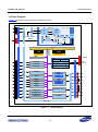
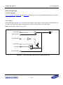
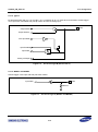
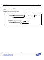
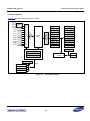
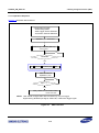
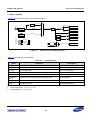
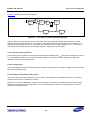
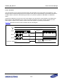
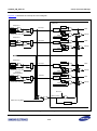
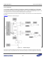
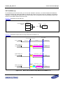
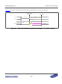
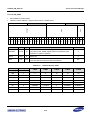
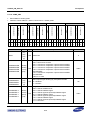
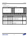
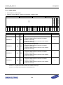
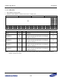
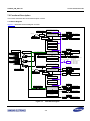
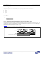
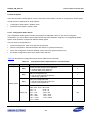
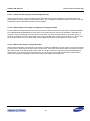
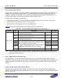
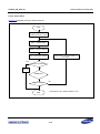
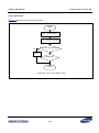
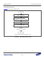
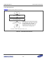
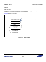
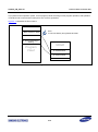
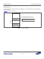
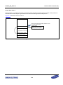
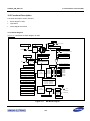
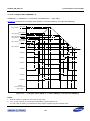
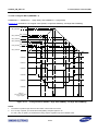
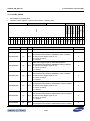
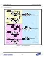
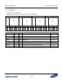
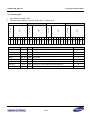
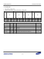
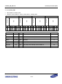
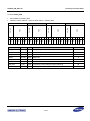
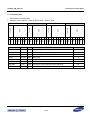
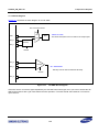
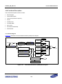
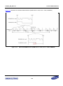
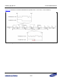
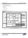
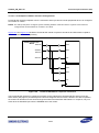
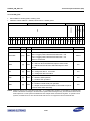
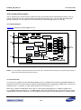
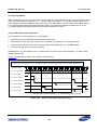
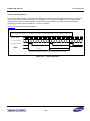
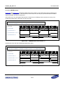
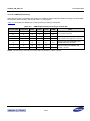
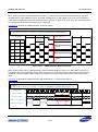
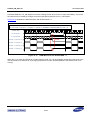
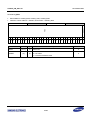
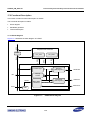
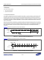
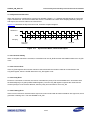
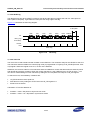
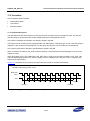
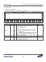
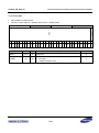
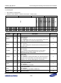
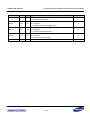
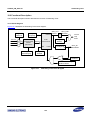
S3FN429_UM_REV1.20 14 Pulse Width Modulation 14.2 Functional Description The functional description section includes: Block Diagram General Description Clock and Operation Frequency Period PULSE Level nPULSE Width IDLE Level Parameter Relationship Extension Bit 14.2.1 Block Diagram Figure 14-1 illustrates the Pulse Width Modulation (PWM) block diagram. INTMASK PWM Start Interrupt PCLK FIN Pre-Scale N PWM_CDR: DIVN Divider M PWM_CDR: DIVM PWM Stop Interrupt INTMASK PWMCLK PWM_CEDR :CLKEN INTMASK Period Start Interrupt UP COUNTER PWM_INT INTMASK = PWM_PRDR : PERIOD Period End Interrupt INTMASK PWM_PULR : PULSE Pulse Match Interrupt = PWM Generator PWMx PWM_SR Figure 14-1 Pulse Width Modulation (PWM) Block Diagram 14-2