1
United States Patent [191
[11]
[45]
Stoughton et al.
[54]
EVENT COUNTER AND ACCESS
CONTROLLER
[75] Inventors: Alan M. Stoughton, Vincentown;
Assignee:
Jul. 30, 1985
Primary Examiner-R. L. Moses
Assistant Examiner-David Warren
Attorney, Agent, or Firm-—-Ratner & Prestia
An event counter and access controller system has a
NJ.
central processor unit, memory storage, and operator’s
Danyl Corporation, Moorestown,
NJ.
Apr. 30, 1982
Int. Cl.3 ........................................... .. GOSG 15/00 _
US. Cl. ........... ..
355/14 CU; 377/16
Field of Search ............................. .. 377/8, 15, 16;
355/14 CU; 235/382
References Cited
U.S. PATENT DOCUMENTS
3,427,441
4,249,163
4,531,826
Charles C. Hansen, Sr., Marlton;
John P. Leahy, Mount Laurel;
Robert F. Millar, Lindenwold, all of
Appl. No.: 373,675
Filed:
Patent Number:
Date of Patent:
2/1969
2/1981
Swords ........................ .1 355/14 CU
Maurer et al. .................... ,. 235/381
[57]
ABSTRACT
keyboard, display, badge reader and key switch. The
system may operate in a normal mode, wherein copy
pulses from a photocopier, for example, are counted and
stored in individual user accounts; and in a set-up mode,
wherein accounts may be sorted and examined, may be
made accessible or inaccessible, and may have their
contents changed. When receiving count copy pulses
from an event to be counted, the system certi?es the
validity of the pulses by ?ltering and sampling tech
niques. When an access card is inserted in the badge
reader, the system validates and accounts for skew tol
erance of the card.
10 Claims, 13 Drawing Figures
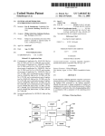
DISPLAY
52
READER
US. Patent Jul. 30, 1985
SheetZoflO
]BATTERY}/e|
72
POWER
/8'
BACK UP
I833’ DN. DET. -—
6?
SWITCH
+V UNREG
60
Q
LOW
\
66]
w- 7,
4,531,826
7
('0'
02's“
=
REF.
\
vs \
_REFRESH PULSE
(FROM CPU)
75
p *??i'gg
a?)
9s
\
RESET
BET.
(FROMLOCALSWI
¥ 19
(
DEBOUNCE
‘SELECT
,7?
58 \65
— DIFFEREN.
s3\
EMIT
4'
a,
4'
4'
%
4'
MT
SWITCH
) (T0 RAM)
f
PWR. UP
/
DET.8DELAY
~
54c
x
K
DET.
(
RESET
‘
64
54b
no CPU)
(TO CPU)’
RAM
(83
59\
2
LOWBAT. _
‘
(FROM DECODER)
54a
5
SW'TCH
69
\74
59
so
43.
-£-——-»
POWER
I00 >
POWER
94(ToRAM)
~ SWITCH
47
—-;
54d
m
H6. 3
_i_
IOI\
92
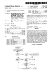
US. Patent 1111.30, 1985
Sheet3of10
4,531,826
I40,.(START)
|42¢ INITIALIZE
(‘.3
I45
TTER
°-'‘-
DISR
~|43
LOW
BATTERY
N
Y
358
DISP
I50‘,
DI(SP
-
.
READY
LOCAL —“@
‘
Y
KEY
I56
Y
-
PRESSED
a
MAINT.
N
SWITCH
-
N
I54
Y
350
I68
use
3
olsP.
N
‘
Y
352
362
'
354
"I
Y
N
[360
Y
@
{364
ACCT.
no
DISP
Y
|7\2\
ACCT.
me —~@
DISP.
Y
N
--@
N
356
174
\DISP. NO.
KEYS
we
COPY LIMIT
358
KEY
D|$R
N
.LQL
PRESSED
'80
"
\ 59825555
F!.4
é
\
D'SR
LIMIT
—--®
US. Patent Jul. 30,1985‘
DISP
ACCT-
Sheet4ofl0
4,531,826
/
BAL.
I
60
SEC.
TIMER
|84
f
I94
I98
TIMER
00m:
Y
we. ACCT. joz
60 sec
TIMER
z-ssc.
TIMER
\2o4
\2
O8
200\ DISAéLE
COPIER
N
' US. Patent
Jul. 30,1985
SheetSoflO
4,531,826
?
DISP. ACCT. ,280
MAINT.
YES
282
KEY
N
:63
Y
DISR
/ 284 I
EXAMINE
286
YES
KEY
Y
SET ACCT.
T0
‘
.N
>
v@)
/288
‘
00
Q)» DISF? TOTAL
KEY
PRESSED
‘
CLEAR
TOTAL
TOGGLE
'
FLAG
(37s
GETNoACCT.
r308
I INC. ACCT
POINTER
ACCT.
3|o
US. Patent Jul. 30, 1985
Sheet 6 of 10
4,5 3 1,826
K378
DISP.
DELETE
"
38%
388
DISF?
E RASED
ACCT. N0.
‘-
39o
DISP.
1
ADD
"“
392
(394
YES
KEY
Y
ACCT. N0.
DISH
jzlo
INITIALIZE
402
DlsR
LDUPLICATE
406\
DIP.
No ROOM]
404
6g [4m
DISR
ERASE
0'89
ERASED
‘
22s
DISP.
CLEARED
22a
DISP.
ALLOWED
( 230
DISF.‘
DENIED
.ZBL
U.S. Patent Jul. 30, 1985
Di SP.
LIMIT
r240
YES
KEY
DISP
MODE
(246
_,242
248
(-250
OAN .HTW
Y
DISR OLD
MAC 8: GET —-
Y
NEW MAC
NEW MAC
[260
(264
262
YES
4,5 3 1,826
Hl LIMIT
244
YES
KEY
DISF!
Sheet 7 of 10
T
266
N
268
Y
TOGGLE
MODE
Y
LOAD NEW
LENGTH
MODE
GET KEY
DISF?
SORT
(me
REORDER
YES
KEY
N
DISP.
LENGTH
(448
DISP. SORT
Y ‘ MEMORY ‘“ COMPLETE-1
420
(424
422
YES
KEY
Y DISR
‘ (43o
OLD
LENGTH 8
GET KEY
426
H G. 58
428
l
US. Patent Jul. 30, 1985
Sheet8 of“)
4,531,826
I52
488
(490
DISP
BAD MAC
BADGE
|N SERT
Y ‘
“To '46
8 AD.
BADGE
BADGE
REMOVED
@
D lsB
INSERT
BADGE
,
496
504
502
FIG. 6
g
VALID
UNLOCK
BADGE
COPIER
@
US. Patent Jul. 30, 1985'
Sheet9of10
C?
FROM 49a
SIO
DISF?
4,531,826
'
"
/
ACCT. BAL.
C0NVERTTOJ6'4
CHARAC.
REG. m5
D's‘? BM‘
.._ll
COPIER
3 J> (D
I
MASK PREV.
2 HOLES
‘
Y (624
MASK EXIT
HOLE
A
MASK OLD
HaE
SOQ
FBG. 6B
US. Patent Jul. 30, 1985
Sheet 10 OflO 4,531,826
FROM I86
_.
EDGE
._ -- ->- T0
PROGRAM
/
(462
(468
l5ms.
VALID
TIMER
,'
COPY PULSE
CARD
T0 I94
'
4,531,826
1
EVENT COUNTER AND ACCESS CONTROLLER
2
him. Also, if the user exceeded his copy count limit, the
controller disabled the copier in the midst of the trans
action, thereby sometimes jamming the copier.
TABLE OF CONTENTS
During set-up conditions, whereby the user initial
izes, denies or permits access to an account, changes
copy count limits, etc., the menu to perform various
Abstract
Background of the Invention
A. Field of Invention
functions has also been inadequate. For example, it has
B. Background Art
not been possible to examine accounts at random or sort
Summary
Brief Description of the Drawings
Description of the Illustrative Embodiment
General Description
ler system. Since it is desirable to maintain account
Power Down Circuit
status in a random access memory (RAM) for as long as
CPU Program Description
Badge Operation
it for sequential examination.
Yet another de?ciency has been the inadequate pro
tection given to the guarding of memory in the control
\
Copy Pulse Certi?cation
BACKGROUND OF THE INVENTION
A. Field of the Invention
This invention relates generally to access control
systems for counting events and more speci?cally to
photocopy counters and access controllers.
B. Background Art
Photocopies have become a major factor in office
overhead costs. With increased speed in copiers today,
numerous copies may be made by any user having ac
cess to a copier, Since such access is not controlled,
copying expenses may multiply rapidly. Furthermore, if
a month, protection of the RAM is paramount. Prior
15
systems have been known to inadvertently destroy
RAM memory during processor failure.
Prior photocopy control systems also exist which
have a microcomputer that interacts with peripheral
devices, such as a keyboard, a display or a badge reader.
However, these systems required cumbersome inter
faces so that the microcomputer could communicate
with these peripherals. Communications was thus slow
and inef?cient.
It is, therefore, an object of this invention to improve
on all of the above de?ciencies and obtain a much better
photocopy controller.
SUMMARY OF THE INVENTION
many users are permitted access to the copier, an ac
counting of how many copies are made by each user is
An event counter and access controller system hav
dif?cult, if not impossible.
ing a central processing unit, a memory storage unit and
Prior systems have been developed to prevent unau
thorized users from gaining access to the copier and also
count the number of copies made by each user. One
an operator’s display and keyboard. The system has
three modes of operation: (1) a normal operating mode,
such prior system is System 80 Transaction Recorder,
manufactured by Danyl Corporation, Pennsauken, N.J.,
the assignee of this application,
mode a machine access code is selected for a ?rst veri?
cation of the access of the user. There is further selected
an individual indenti?cation of each of a plurality of
accounts each corresponding to a different user. Each
account has a corresponding account identi?cation
In order to count the number of copies made by the
user, these prior systems rely on a copy pulse outputted
from the photocopier. Such pulse is present whenever a
photocopy is made by the machine. By counting the
number of copy pulses present, the prior systems deter
mine the number of copies made. The prior systems,
however, leave much to be desired. Since each photo
copier generates unique copy pulse characteristics, each
of the prior systems has to be specially con?gured to
interface with the idiosyncracies of the photocopier.
Such task is complicated since copy pulses vary in am
plitude and duration from one copier to another. More
over, prior systems are susceptible to the presence of
noise on the copy pulse lines, thereby erroneously
counting pulses.
Prior systems also have the ability to prevent unau
thorized users from accessing the photocopier. Users
(2) a set-up mode and (3) a local mode. In the set-up
number and copy count total. Further, in the set-up
mode, the accounts may be sorted by account identi?ca
tion number and examined for individual copy count
totals. During the normal mode, the photocopier is
enabled when there is a proper machine access code and
45 account identi?cation number and the copy count has
not been exceeded. Further, in accordance with the
invention, there is provided pulse certi?cation in which
both the leading edge and the trailing edge of a photo
copier pulse are individually validated.
BRIEF DESCRIPTION OF THE DRAWINGS
FIG. 1 illustrates in basic block diagram form a pho
tocopy counter and access controller system embody
are prevented from accessing the copier by the use of 55 ing the invention;
FIG. 2 illustrates in basic block diagram form the
badge reader devices or personal account number veri
power
down circuit shown in FIG. 1;
?cation devices. Unless a user has a valid badge or an
FIG.
3 illustrates in basic block diagram form the
authorized account number, access is denied. Here too,
prior systems leave much to be desired. Badge reader
devices have been known to be inaccurate, sometimes
badge reader shown in FIG. 1;
FIGS. 4-4A taken together form a functional flow
having problems identifying a particular badge. Also,
diagram of the program performed by the system
account number veri?cation devices have proven to be
shown in FIG. 1;
FIGS. 5, 5A and 5B taken together form a functional
cumbersome to update, being dif?cult to modify old
account numbers or add new account numbers.
In addition, it has been dif?cult to examine each indi
vidual account number and view its current copy status.
?ow diagram of the set-up mode performed by the
system shown in FIG. 1;
FIG. 6-6A taken together form a functional flow
The user has had dif?culty in determining how many
diagram of the badge operation performed by the sys
copies he has made and how many more are allotted to
tem shown in FIG. 1;
3
4,531,826
FIG. 6B is the skew tolerance routine performed at
block 500 of FIG. 6; FIG. 7 is the copy pulse certi?ca
tion routine performed at block 192 of FIG. 4A;
FIG. 8 is a representation of an access card used in
the badge reader shown in FIG. 1.
DESCRIPTION OF THE ILLUSTRATIVE
EMBODIMENT
General Description
FIG. 1 shows the general con?guration of photocopy
counter and access controller system 10 comprised of
central processor unit (CPU) 12, random access mem
4
amount of time causes a reset command to be issued on
line 96 from power down circuit 20. The power down
circuit will be discussed in detail later.
Thus, CPU 12 communicates with RAM 14 only
after the chip select signal from decoder 22 has been
enabled by power down circuit 20. On the other hand,
no chip decoding is necessary when CPU 12 communi
cates with ROM 16. The program ROM is read by CPU
12 by way of data bus 23 and addressed by address bus
21, whenever it has been enabled by control line 11.
Since there is only one program ROM, no decoding is
necessary.
ory (RAM) 14, read only memory (ROM) 16, address
It will be understood that CPU 12 may be a single
latch 18, decoder 22, input/output (I/O) control 24,
chip microcomputer, such as the 8031 microcomputer
power down circuit 20, serial port 26, copier interface
circuit 28, and I/O subsystem 10a. As shown, I/O sub
system 10a contains keyboard 42, display 50, user opera
tor switch 44, and badge reader 54. All communications
between the I/O subsystem and the CPU are done by
way of I/O control 24. U0 subsystem 10a also contains
which has capability of accessing memory and I/O
2764 chip for storing the program. The RAM consists
keyboard scan decoder and driver 40, character de
dress space. The ?rst two are blocks of CMOS battery
coder 45, display driver 48, and segment driver 52.
CPU 12 is the “brains” of the system. All program
execution is performed within it. While the program is
executed within the CPU, it is actually stored in ROM
16 and the CPU fetches each instruction to be executed
from ROM 16. Aside from program instructions, there
is also data to be manipulated and stored. As in program
execution, all data manipulation (for example, add, sub
tract, compare, etc.) is performed in CPU 12 but stored
in and read from RAM 14. Besides program instruction
and data, there is also I/O commands and data to be
controlled. The CPU reads and writes data and com
outside of the 8031. The ROM may be a 2716 or 2732 or
of 2048 bytes of memory for data storage and may be
comprised of 5514 or 6514 components. There are three
separate blocks which may be accessed in the data ad
backed-up RAM each being a 1,024 byte block. The
RAM, however, requires decoding by decoder 22,
which may be one chip such as the 74L OO decoder.
Finally, address latch 18 may be a 74LS373 latch for
latching address bits from data bus 23.
Also shown in FIG. 1 is copier interface circuit 28
which is the means by which CPU 12 may control an
30 external device, such as a photocopier (not shown). It
will be understood that copier interface circuit 28 is of
a conventional type and may be similar to the interface
circuit disclosed by the Danyl System 80, User Manual
which is incorporated herein by reference. The general
mands from and to I/O subsystem 10a by way of I/O
control 24.
35 con?guration of badge reader 54 is also disclosed
To allow CPU 12 to access RAM 14, ROM 16, or
I/O control 24, the CPU places the ?rst portion of an
address in address latch 18 by way of data bus 23, and
the second portion of the address is placed directly onto
address bus 21. The ?rst portion of the address is
therein. Control signals are sent from CPU 12 to copier
interface circuit 28 by way of line 27. Such control
signal may be an on/off message from CPU 12 which
corresponds to an enable/ disable state on line 19 for the
photocopier being controlled.
latched, when an address latch enable is placed on line
External events, such as copy pulses, also may be
13. After the latching of the ?rst portion of the address,
interfaced and counted by way of copier interface cir
cuit 28. It will be understood that such copy pulses are
data bus 23 is used for data transmission or reception.
generated by photocopying devices for purpose of
The output of address latch 18 is decoded by decoder
22 in order to select the proper chip in RAM 14 by way 45 maintaining counts of the number of photocopies made
of chip select line 92. As shown, the chip selects ?rst go
by such devices. Since the signal characteristics of the
through power down circuit 20 by way ofline 83 so that
the data in the RAM may be protected when system
power is off, or when power is being cycled on or off.
If power down circuit 20 senses proper voltage condi
copy pulses are different from one photocopier to an
tions, it will permit chip selection in RAM 14. Once
permitted, data may be read from or written to the
selected address in RAM 14 by way of data bus 23.
The power down circuit also provides other func
tions. It contains a battery backup for the RAM and
supplies backup power by way of line 94. In addition, it
generates several signals to CPU 12. One such signal
placed on line 67, is an advanced warning that system
power is being shut down. Another signal, placed on
line 100, is a warning that the battery power is low and,
therefore, the battery should be replaced. Still another
other, copier interface circuit 28 may accommodate
various types of inputs from the photocopy devices.
Such inputs, for example. may be l20 VAC, 24 VDC
and 5 VDC. The time duration of these pulse inputs
may also be of various lengths, for example, they may
vary from a few milliseconds to few tenths of seconds.
When a copy pulse is detected on line 19 by the copier
interface circuit, the pulse is placed on line 27 for fur
ther timing and evaluation by CPU 12. The timing and
evaluation performed by CPU 12 on the copy pulses
will be explained in detail later.
CPU 12 may also communicate with other peripheral
devices (not shown) by way of serial port 26. It will be
understood that serial port 26 is of a conventional type
and may be an RS422 port. Such port permits periph
the CPU whenever power comes on or off and when
eral devices to control system 10, maintain the system,
ever a program malfunction is detected.
and pass data to and from the system.
Another function of power down circuit 20 is to 65
Still referring to FIG. 1, there is shown I/O control
monitor CPU 12 activity. A signal, placed on line 87, is
24. CPU 12 communicates with U0 subsystem 100
signal, placed on line 96, provides a reset command to
issued by CPU 12 indicating that the program is running
correctly. Failure to issue this signal within a certain
through I/O control 24 by way of keyboard data bus 41,
U0 address bus 43, U0 data bus 47 and blanking 45. It
5
4,531,826
will be understood that 1/0 control 24 may be an 8255A
6
bus 47 supplies segment data to the display; when blank
chip having three 8 bit I/O ports that are programmable
ing 45, however, is active, I/O data bus 47 supplies
as input or output. I/O control 24 may communicate
badge reader data to the CPU.
It will be understood that in order to handle the real
with keyboard 42, which may contain, for example, 36
keys for use by a key operator; display 50, which may
time tasks required for the display refresh, keyboard
be a vacuum ?uorescent display, for example, having a
scan, key operator scan, and badge reader scan at a rate
which is “?icker” free to the user, the CPU has a timer
16 character 14 segment display; badge reader 54 for
user identi?cation; and key operator switch 44 which
which interrupts the processor every 500 microseconds.
may be a three position switch for setting the mode of
Thus, display character updates and keyboard scans
system operation. As will be explained in detail later, 0 occur at a 500 microsecond rate which is sufficiently
three modes of system operation are possible: local
fast to provide “flicker” free operation. Furthermore,
mode, normal mode and set-up mode.
since CPU software execution times are based on an
I/O address bus 43 provides two functions in. 1/0
other timer, the display and keyboard scanning updates
subsystem 100. It addresses the display character posi
are independent of software execution.
tion which is to be displayed for a certain period of time
It will also be understood that character decoder 46
in display 50 and also selects the keyboard column
may be comprised of two 4028 and one 74142 decoders,
which is to be examined for the same period of time.
drivers 48, 52 may be of conventional UDN 6118 buf
With an address on 1/0 address bus 43, character de
fers/drivers, scan decoder 40 may be a 74LSl45 de
coder 46 decodes the character position to be displayed.
coder, and display 50 may be a conventional FIPl
The character position is then selected in display 50 by 20 6A5R.
way of drivers 48. Once the character position is se
In operation, the protocol between 1/0 control 24
lected, the segment information present on 1/0 data bus
and I/O subsystem 100 is as follows: If, for example, an
47 is displayed in display 50. Drivers 52 contain the
address of “O” is placed on 1/0 address bus 43, key
buffers/drivers that convert the I/O data bus segment
board scan decoder 40 causes keyboard 42 to select
25
data into proper drive levels for the display.
column “0” of the keyboard. Any keys pushed in col
After a character is displayed for the allotted amount
umn “O” are then presented on keyboard data bus 41.
of time, the character decoder is disabled or blanked for
The same address “0” on 1/0 address bus 43 causes
a speci?ed amount of time before the next character is
character decoder 46 and drivers 48 to enable or drive
displayed. Such disabling is provided by blanking line
character position “0” in display 50. At the same time,
1/0 data bus 47 presents segment data, comprising the
desired character to be displayed to character position
45. During this blanking time, segment information is
removed from l/O data bus 47 and the same bus is put
into an input mode, whereby data may flow into 1/0
control 24. The data put onto I/O data bus 47 during the
blanking time are badge reader 54 data to be read by
“0” of display 50. During this time blanking line 45 is
inactive, so that badge reader 54 is disconnected from
1/0 data. bus 47. This condition remains until it is time
to go to the next character display position and the next
1/0 control 24. The operation of badge reader 54 will
be explained later.
When the blanking time is completed by the removal
of the blanking signal from line 45, the I/O data bus is
keyboard column position.
Next blanking is asserted by activating blanking line
45. As a result, the display and keyboard are no longer
returned to the output mode to prepare for display of
the next character. After a new display character posi
tion is selected by decoder 46, new segment data are
placed onto I/O data bus 47 from 1/0 control 24. In this
manner, I/O data bus 47 is a bidirectional bus, providing
being driven and the I/O address bus is ignored. The
badge reader, however, begins to present data to I/O
data bus 47 for transmission back to CPU 12. This con
dition remains until the blanking signal is removed.
Upon removal of the blanking signal, badge reader 54 '
segment data to the display during non-blanking periods
and badge reader data to the CPU during blanking
periods.
45 is disabled. In addition, new address data are presented
on 1/0 address bus 43 to select a new display character
position and a new keyboard column to be scanned.
Moreover, new segment data are presented on 1/0 data
bus 47 to indicate the character to be-displayed in the
-
As already mentioned, I/O address bus 43 selects the
keyboard column to be examined during the same time
as it selects the display character position. Such selec
tion is done through keyboard scan decoder 40, which
decodes the proper keyboard column in keyboard 42.
The row information of any key pushed in the selected
column being scanned may be read by CPU 12 by way
of keyboard data bus 41 and I/O control 24.
It will be noted that operator switch 44 is also
scanned, upon being selected by 1/0 address bus 43 by
way of scan decoder 40. When the operator switch is
scanned, the switch position selected is read by CPU 12
by way of keyboard data bus 41. Thus, keyboard data
bus 41 provides the CPU with information not only of
any key pushed in keyboard 42 but also of the switch
position selected by operator switch 44.
newly chosen character position. In this manner, I/O
data bus 47 is multiplexed between outputting display
50 data and inputting badge reader 54 data.
The operation of badge reader 54 will now be ex
plained. The badge reader is shown schematically in
55
FIG. 3. It comprises emitters 54a, which may be a string
of 12 diode emitters, for example. The emitters, which
emit radiation in the infrared region, are separated phys
ically on one side ofa gap in a surface. On the other side
of the gap are located correspondingly opposing detec
tors 5412, which may be 12 in this example. Detectors
5412 are photo transistors which are sensitive to the
infrared emissions. When a user’s badge is passed
through the gap, holes in the badge are aligned with the
It will further be noted that keyboard data bus 41 is a
emission paths from the emitters to the detectors. Thus,
unidirectional bus and is only utilized for sending data
to the CPU. The 1/0 data bus, however, is a bidirec 65 a particular combination of holes in the badge will
allow certain emissions from emitters 54a to be detected
tional bus which can provide segment data to the dis
by detectors 54b. The detected emissions are then pres
play and then provide badge reader data to the CPU.
ented to switch 54c by way of line 5441.
During periods when blanking 45 is inactive, I/O data
7
4,531,826
8
Switch 540 contains, in this example, 12 Schmidt
triggers, which may each be triggered by a correspond
ing photo transistor in detectors 54b. It will be under
stood that switch 540 may apply the triggered combina
tions identifying the badge onto I/O data bus 47. As
a valid state during the delay, circuit 64 removes the
reset condition from line 65, thereby causing the reset to
be removed from line 96 to the CPU.
Also shown in FIG. 2 is power down detector 66,
mentioned earlier, such data are not applied until the
blanking signal is asserted on line 45.
ent at the system wall plug) present on line 103. If the
It must be mentioned at this point that the badge,
when inserted inside badge reader 54, has a certain
amount of skew tolerance. It is, therefore, possible to
power down detector 66, which then sends an advance
insert the badge with slight misalignment, causing the
badge reader to send incorrect identi?cation data to
CPU 12. The program, however, in CPU 12 checks the
validity of the badge reader and insures that the skew
tolerance does not create incorrect identi?cation. This
skew tolerance routine will be described in detail later.
Power Down Circuit 20
Operation of power down circuit, shown in FIG. 2,
will now be described. In general, the power down
circuit provides two functions. First. it assures that,
when power is applied or turned off, CPU 12 is reset.
which monitors the unregulated system voltage (pres
system is unplugged from the wall, the voltage on line
103 would begin to decay. Such condition is sensed by
power notice to CPU 12 by way of line 67. Upon being
noti?ed of a power down initiation, CPU 12 stops any
new accesses to the RAM. Furthermore, power down
delay 68 generates a reset signal onto line 69, which
causes CPU 12 to be reset by way of reset switch 74.
The same reset signal is also sent to RAM chip selection
switch 70, which prevents any further chip selections in
the RAM. As shown, switch 70 receives, by way of line
83, RAM chip selection signals from decoder 22 (FIG.
1). Upon being noti?ed of a power down condition by
the reset signal on line 69, switch 70 inhibits RAM chip
selections from line 83 from reaching the RAM by way
Also, if for any reason the CPU becomes invalid, a reset
is sent to CPU 12 to begin operations from start. Sec
of line 92.
ond, it assures data integrity of RAM 14. If system
20 is to assure that power is always supplied to the
RAM in order to insure data integrity. This is accom
power is lost, battery backup power is supplied the
RAM. Also, it prevents CPU 12 from accessing RAM
The second function provided by power down circuit
plished by backup switch 72. Under normal conditions,
system power from line 101 is provided to the RAM.
During power up or power down conditions, as already
being cycled on or off.
In operation, refresh pulse 87 is supplied by CPU 12 30 mentioned, a reset signal is provided on line 69. This
reset signal causes backup switch 72 to switch-in battery
every 500 microseconds. while the processor is execut
power from battery 61 to the RAM by way of backup
ing its programs. Such a pulse, it will be understood, is
14, whenever an invalid condition exists or power is
present whenever CPU 12 is performing properly. If for
some reason, for example, noise or power disruption,
program execution becomes invalid, the refresh pulse 35
would be missing on line 87.
Missing pulse detector and oscillator 76, it will be
understood, comprises two mono-stable multivibrators
in series forming an astable multivibrator. So long as a
refresh pulse is present at the ?rst mono-stable multivi
brator, the mono-stable is reset and is started again on its
power line 94. Of course, after system voltage is greater
than ‘the battery voltage, RAM power is switched back
to system power from line 101.
To assure the integrity of battery 61, low battery
detector 60 senses the voltage adequacy of the battery.
Thus, the voltage level of battery 61 is compared to
reference voltage 62. Whenever the battery voltage
falls below the reference voltage, line 100 informs the
CPU that the battery voltage is low and the battery
time-out. If, however, a refresh pulse is missing on line
87, the ?rst mono-stable times out its period and will,
should, therefore, be replaced.
is an indication that the CPU should be reset. The reset
pulse on line 75 enters processor reset switch 74 which
for example, if system 10 is not performing properly or
CPU 12 is denying access to the photocopier. It will be
understood that the local mode is selected by a local
switch (not shown) that overrides the CPU and causes
a relay in copier interface circuit 28 (FIG. 1) to enable
Finally, power down circuit 20 provides a means to
subsequently, cause the second mono-stable multivibra
reset CPU 12 whenever the operator has selected the
tor to start its timing period. At the end of its period, a 45 local mode in order to override the CPU and permit
reset pulse is placed onto line 75. Such a pulse on line 75
access to the photocopier. Such a situation may arise,
buffers and drives the reset pulse to the CPU by way of
line 96. Thus, every time the refresh pulse is missing
from CPU 12, the missing pulse detector and oscillator
causes the CPU to be reset and start its program execu
tion from the start.
Also shown in FIG. 2 is power up detection and
the photocopier.
The closure of the local switch is sensed by debounce
delay circuit 64 which detects the power up phase of 55 _by way of line 89. Debounce 80 is a low pass ?lter
which ?lters out any noise on line 89. This prevents
system 10. When power is turned on, the system voltage
CPU 12 from being reset during false local switch clos
on line 101 begins to rise until it reaches +V. So long as
ings.
The output of debounce 80 is differentiated by
system voltage 101 is less than reference voltage 62,
differentiation circuit 78, which provides a pulse on line
sensed by way of line 59, power up detect and delay
77 to be sent to missing pulse detector and oscillator 76.
circuit 64 produces a reset condition on line 65. The
In turn, the missing pulse detector and oscillator pro
reset condition on line 65 passes through power down
vides a single pulse on line 75 to reset CPU 12 by way
detector 66, power down delay 68, and reset switch 74,
thereby producing a reset condition on line 96 which
of reset switch 74. Thus, CPU 12 is reset once, when the
then causes CPU 12 to be reset.
local switch is activated by the operator.
It will be understood that debounce 80 may also pro
When system voltage 101 becomes greater than refer 65
ence voltage 62, the power up detection and delay cir
vide a direct signal (not shown) to CPU 12 by way of
cuit 64 begins a delay timer. After the delay has timed
line 79. Such a direct signal may notify CPU 12 that
out and, assuming that the system voltage has stayed in
system 10 is in the local mode.
9
4,531,826
10
pressed (block 152); a copy pulse from the copier inter
CPU Program Description
face circuit to be received (block 154); or the mainte
nance or set-up switch to be activated (block 156). If the
CPU 12 programs may be divided into three func
tional parts: a normal mode, a set-up mode, and a local
mode. The normal mode controls operations between
system 10 and an operator wishing to gain access to the
START key is pressed (block 350), MAC validity is
checked (block 166); if the START key is not pressed,
the program checks whether the CANCEL key has
photocopier. The set-up mode controls operations be
been pressed (block 352). If the CANCEL key has been
pressed, then the program loops back to block 146 indi
cating that all previous key inputs are to be ignored. If
tween system 10 and an operator wishing to set-up
system 10 for use by others or wishing to verify ac
counts in the system. Finally, the local mode is used to
override system 10 control and permit access to the
the CANCEL key has not been pressed, the program
checks how many keys have been pressed (block 354).
photocopier regardless of system 10 operation.
If more than the maximum number of keys have been
An important feature of the set-up mode are various
menu items that allow various operations to be per
formed. One such menu item is the ability to examine
each user account and view its current copy status; each
account may be randomly or sequentially accessed.
pressed, for example 13 keys, then TOO MANY is
displayed on the display for two seconds (block 360)
and the program loops back to block 146. If the key
limit has not been reached, then the keys entered thus
far are displayed (block 356). The program then waits
for the next key to be pressed (block 358) and then loops
Whether an account is permitted or denied access is also
back to block 350.
shown to the viewer.
Another menu item is the machine access code 20
Returning to block 350, if the START key has been
(MAC) which may be changed by the operator. It will
pressed, MAC validity is checked (block 166). MAC, as
be understood that MAC may be a three-digit code and
already mentioned, is a machine access code and, for
example, may be comprised of three digits. If the MAC
acts as a security key. Another menu feature is the selec
digits pressed are incorrect, then BAD MAC is dis
tion of an upper copy count limit for each account
which may be set to zero (denying access) or 99,000, for 25 played for 2 seconds on display 50 (block 168) and the
example.
program loops back to block 146. If the MAC is correct,
then the program checks whether the entered account
Yet another menu feature is the mode which allows
the remaining copy balance to be displayed in an incre
menting or decrementing mode. If an operator selects
number (which may be, for example, a 2-digit code
entered by the operator) is in memory (block 362). If it
the incrementing mode, then the gross number of copies 30 is not, then BAD ACCOUNT is displayed for 2 seconds
made is displayed during copying in an incremental
(block 364) and the program loops back to block 146. If
manner (l, 2, 3, 4, etc.) If, however, the decrementing
it is in memory, then the account is checked to see
mode is selected, then the balance is displayed in a de
whether access has been denied (block 170). If it has,
DENIED is displayed for 2 seconds (block 172) indicat
creasing balance (1000, 999, 998, etc.).
Another menu item is the sorting feature. The sorting
feature permits accounts to be examined in an increasing
alpha numeric sequence. This aids the operator in exam
ining the status of accounts in a logical sequence.
ing that access has been denied to that account and the
program loops back to block 146. If, however, access is
, permitted, the program checks whetherthe account has
exceeded its copying limit (block 174). Assuming that
the limit has been exceeded, LIMIT is displayed on
The above completes a general description of the
set-up mode. A more detailed description of the set-up 40 display 50 (block 176) and the program loops back to
block 146. If the limit has not been exceeded, the copier
mode will be described later. A general description of
is enabled by way of the copier interface (block 180)
the normal mode will now be given.
and the program proceeds to block 182 (FIG. 4a).
In the normal mode, the operator is first noti?ed that
Still referring to FIG. 4, if the set-up switch is se
system 10 is ready to accept inputs. In order to gain
lected (block 156), the program loops to block 280
access to the system, the operator must first enter the
(FIG. 5), which will be described later. If a key has not
MAC number by keyboard. Secondly, he must enter his
been pressed on the keyboard (block 152) and a copy
account number correctly by keyboard or by badge.
pulse has been received (block 154), then LOCAL is
Assuming that the MAC number and the account num
displayed (block 358) indicating that the local mode has
ber are correct, system 10 will next check the account
number’s copy balance. If the copy balance has not 50 been selected. In addition, in order to keep track of the
number of copies made in the local mode, the program
sets the account code to 100, for example, and maintains
count of the copies made, as will be explained later.
or decrementally. If the operator exceeds his copy allot
The method in which the number of copies made is
ment during the transaction, the system permits the
photocopier to complete the transaction. This prevents 55 counted is shown in FIG. 4a. As shown, the program
displays the account’s balance according to the mode
jamming of the photocopier. Once the transaction is
selected (block 182). If the incrementing mode is se
completed, system 10 does lock out the operatorand
lected, the gross number of copies made to date is dis
effectively terminates his activity.
played; if the decrementing mode is selected, only the
A detailed flow diagram of the system 10 program is
shown in FIGS. 4, 4a, 5, 5a and 5b. The program will 60 balance remaining is displayed. The program also acti
vates a 60-second timer (block 184) so that if no activity
now be described serially. Beginning with START 140,
is present for 60 seconds, the copier is disabled.
the program initializes all functions and checks the
Block 186 checks whether a copy pulse has been
battery (block 142). If the battery is OK (block 146),
received. If not received within 60 seconds (block 188),
READY is displayed to the operator (block 150); if the
reached its maximum, the photocopier is unlocked and
the remaining copy balance is displayed, incrementally
battery is low, Low BATTERY is displayed (block
65
the copier is disabled (block 200) and the program loops
148).
back to START 140. If the 60-second timer has not yet
At this juncture, as shown, the program waits for one
of three things to occur: a key on the keyboard to be
timed-out (block 188), the program checks whether the
COMPLETE key has been pressed (block 190). If not
11
4,531,826
12
pressed, the program loops back to check whether a
reached its maximum, for example 101 (block 310). If
copy pulse has been received (block 186); if COM
(block 196). Upon completion of the 2 seconds (checked
the maximum account has not been reached, the pro
gram displays that account and its copy total (block
288). If the maximum has been reached, the program
by block 198), the copier is disabled and the program
loops to the delete handler (block 378, FIG. 50).
PLETE has been pressed, a 2-second timer is started
loops back to START 140.
Finally, if the NO key is pressed (block 312), the
Referring back to block 186, if a copy pulse has been
program loops directly to the delete handler (block 378,
received, a copy pulse debounce timer is started (block
FIG. 5a). “DELETE?” is then displayed on display 50.
192). The debounce timer monitors whether the copy
The program then waits for the YES or NO key to be
pulse is present for some minimum period. If present for 10 pressed (block 380). If YES is pressed, the program
the correct minimum period, the copy pulse is assumed
waits for the operator to key in the account number to
to be valid; otherwise, the copy pulse is assumed to be
be deleted (block 382). A check is then made of whether
noise and is ignored. If the copy pulse is valid (block
the account exists (block 384). If it exists, the account is
194), the selected account register is incremented (block
deleted and ERASED is displayed for 2 seconds (block
202). The 60-seconds timer is restarted (block 204) and,
388). If it does not exist, however, BAD ACCOUNT is
if the 2-second timer is running (block 206), the 2
displayed for 2 seconds (block 386).
second timer is also restarted (block 208). The program
then loops back to wait for the next copy pulse. This
loop continues as long as copy pulses are received. If no
copy pulses are received for the timed period, the
copier is disabled (block 200).
If the set-up mode has been selected (block 156, FIG.
4), the program jumps to block 280, shown in FIG. 5.
At this juncture, “ACCOUNT MAINT?” is displayed.
The program then checks whether a YES or NO key is 25
pressed by the operator (block 282). If NO is pressed,
the program jumps to the initialization handler (block
210, FIG. 5a); if YES is pressed, “EXAMINE?” is dis
played on display 50 (block 284). The program then
again checks whether a YES/NO key is pressed (block
286). If NO is pressed, the program jumps to the delete
handler (block 378, FIG. 5a); if YES is pressed, the
account pointer is set to zero, which corresponds to the
If the NO key is pressed (block 380), “ADD?” is
displayed (block 390). The program then waits for the
operator to press either YES or NO (block 392). If YES
is pressed, the program waits for the operator to key in
the account number to be added (block 394). A check is
made to determine whether the account already exists
(block 396). If already in existence, DUPLICATE is
displayed for 2 seconds (block 402); if not a duplicate,
another check is made to determine if there is room in
memory to add the account (block 398). If there is no
room, NO ROOM is displayed for 2 seconds (block
404). If there is room, however, the account is added
and ADDED is displayed for 2 seconds (block 400).
The program then loops back to block 390.
If the NO key is pressed (block 392), “INITIAL
IZE?” is displayed (block 210). Again, the program
waits for a YES or NO key to be pressed (block 212). If
juncture, the account number and its copy total are 35 NO is pressed, the program jumps to the limit handler
(block 240, FIG. 5b). If YES is pressed, “ERASE?” is
displayed on display 50.
displayed (block 406). Again, the program waits for a
At this point, one of ?ve keys may be pressed on the
YES or NO key to be pressed (block 408). If YES is
keyboard: the CLEAR TOTAL key, PER
pressed, the memory in the RAM is erased and
MIT/DENY key, MANUAL ENTRY key, YES key,
ERASED is displayed for 2 seconds (block 410).
or NO key. If CLEAR TOTAL IS PRESSED (block
If NO is pressed in block 408, the message
292), the program checks whether the account is denied
“CLEAR?" is displayed (block 214). The program then
(block 294). If the account is denied, the program loops
waits for a YES or NO key (block 220). If YES is
back to block 290 to await the pressing of another key.
pressed, the memory is cleared and the display shows
If the account is not denied, the account’s total register
in RAM 14 is cleared (block 296) and control passes 45 CLEARED for 2 seconds (block 226).
If NO is pressed in block 220, the message “AL
back to block 288, which updates the copy total to zero.
LOW?” is displayed (block 216). A YES key subse
If the PERMIT/DENY key is pressed (block 302), a
?rst account location in RAM 14 (block 288). At this
permit/deny flag is toggled (block 298; if previously it
quently pressed (block 222) noti?es the program to
has been “1,” upon being toggled it becomes “0,” or
allow access to all accounts and display ALLOWED
vice versa. It will be understood that permitting or
denying is a method to selectively allow or disallow
permitted, then an operator using the copier is only
for 2 seconds (block 228).
If NO is pressed in block 222, the message “DENY?”
is displayed (block 218). The program then waits for a
YES or NO key to be pressed (block 224). If YES is
checked for total copy limit. If an account is denied,
pressed, access to all accounts is denied and DENIED
someone’s use of his account number. If an account is
however, although a valid code is entered, the operator 55 is displayed for 2 seconds (block 230). If NO is pressed
in block 224, the program jumps to the limit handler
is denied access to the copier.
If the MANUAL ENTRY key is pressed (block 370),
the program waits for the operator to key in the account
number of interest (block 372). A check is then made to
determine whether the account number is in the RAM
(block 374). If it is in memory, the program displays the
account and copy total (block 288). If it is not in mem
ory, BAD ACCOUNT is displayed for 2 seconds (block
376) and the account pointer is set to zero (block 288).
(block 240, FIG.‘ 5B).
Referring now to FIG. 5B, there shown is the limit
handler, wherein “LIMIT?” is displayed on the display
(block 240). If YES is then pressed (block 244, the cur
rent copy limit is displayed and the program waits for
the new copy count limit to be keyed in (block 246). A
check is then made to determine whether the new copy
limit exceeds the allowed maximum, for example 99,000
If the YES key is pressed (block 306), the account 65 copies (block 248). If it does, HI LIMIT is displayed for
pointer is incremented sequentially (block 308) so that
2 seconds (block 242). If it does not, the new copy limit
the operator may view the next account’s copy total.
The program then checks whether the pointer has
is loaded into memory (block 250) and the program
loops down to the MAC handler (block 252).
13
4,531,826
14
BADGE is displayed (block 494) and the program waits
until the badge is removed (block 495).
Referring to block 252, the program displays
“MAC?” on the display. If YES is subsequently pressed
(block 254), the current MAC number is displayed and
Once the badge is removed, or if the badge has never
been inserted, the message INSERT BADGE is dis
the program waits for a new MAC to be keyed in (block
256). The new MAC is then loaded into memory (block
258), and the program loops down to the mode handler
played (block 496). The program then waits for the
badge to be inserted (block 498). After the badge is
inserted, a validity check is made on the badge (block
(block 260).
rementing manner. The mode handler begins with the
500). The badge validity check will be described in
detail later. If the badge is invalid, BAD BADGE is
displayed (block 494); if a valid badge has been inserted,
display showing “MODE?” (block 260). If the YES key
is then pressed (block 262), the current mode (incre
however, the program also checks whether the account
requirements have been met (block 502). If the account
As already mentioned, the mode handler permits
copy counts to be displayed in an incrementing or dec
requirements have not been met, an error message is
menting or decrementing) is displayed and the program
displayed (block 506), as has been described earlier. The
waits for a YES or NO key (block 264). If YES is
pressed (block 266), the program jumps down to block 15 program then waits for the badge to be removed (block
508) and loops back to block 146, shown in FIG. 4. If
412; if NO is pressed (block 268), then the mode is tog
the account requirements have been met, the copier is
gled (block 270) and the program loops back to display
the new mode. In this manner, the mode can be toggled
unlocked by way of the copier (block 504).
Referring next to FIG. 6A, after the copier is enabled,
to be incrementing or decrementing.
The sort handler begins in block 412 wherein
the account balance is displayed (block 510), as has
already been described. If a copy pulse is received next,
“SORT?" is displayed on display 50. If YES is subse
the copy pulse is debounced and checked for its validity
quently pressed (block 414), the accounts in memory
are reordered into ascending alpha numeric order
(blocks 512, 516, 518). Ifa valid copy pulse, the account
register is incremented and the new balance is displayed
(block 416) and SORT COMPLETE is displayed for 2
(block 520). The program then waits for the next copy
seconds (block 418). The program then loops down to
pulse to arrive.
the length handler (block 420).
display (block 420). If NO is pressed (block 422), con
If a valid copy pulse has not been received, the pro
gram checks whether the badge has been removed
trol passes back to the beginning of the maintenance or
(block 514). If the badge has not been removed, the
set-up routine (block 280). If YES is pressed, the current
program waits for the next copy pulse to arrive. If the
badge has been removed, a two-second delay is started
The message “LENGTH?” is then displayed on the
length is displayed and the new length may now be
entered (block 424). The new length may be, for exam
ple, between 1 and 8 inclusive, and is used to format
to check for remaining copies (block 522). The two
second delay insures that all copies made are counted by
system 10, although the badge has been removed. Thus,
display 50. If the YES key is pressed (block 426), the
current length is saved and control passes to the begin 35 as long as new copy pulses are received, the new pulses
are counted by the program (blocks 524 and 526). If no
ning of the set-up routine (block 280). If not, a check is
new copy pulses are received within two seconds, the
made to determine whether the 1-8 key is pressed
copier is disabled (block 528) and the program jumps to
(block 428). If it is these keys, the new length is loaded
block 146, shown in FIG. 4.
into memory; otherwise, it is ignored. The new length is
Referring now to the badge validity check (block
then displayed (block 424) and if YES is pressed (block
500), it must be ?rst recalled that a badge when inserted
426), control passes to the beginning of the set-up rou
in badge reader 54 has a certain amount of skew toler
tine.
Badge Operation
The badge operation routine, shown in FIGS. 6, 6A
and 6B, will now be described. It will be understood
that the badge operation routine is part of the program
performed by CPU 12. Referring to FIG. 6, there is
shown decision block 152 which, it will be recalled, has
been discussed earlier in FIG. 4. It is at this junction that
the badge operation routine begins.
The routine checks whether the CANCEL key has
been pressed (block 480). If it has been pressed, the
45
ance. The function of the badge validity routine is,
therefore, to check for proper badge identi?cation,
taking into consideration the skew tolerance of the
badge.
One example ofa badge access card is shown in FIG.
8. As shown, badge 700 has six rectangular holes, 710
through 720. Each horizontal pair of holes represents a
single character. For example, the three pairs shown
represent three characters: pair 710, 712 represents “2”;
pair 714, 716 represents “0”; and pair 718, 720 also rep
resents “O." Badge 700 may be inserted into badge
program jumps to block 146, shown in FIG. 4. Ifit has
reader 54 in a downwardly direction shown by arrows
not been pressed, the program checks whether a third
722. Consequently, upon being inserted in the slot, if no
skew is present, the badge reader will ?rst detect holes
718, 720; next it will detect holes 714, 716; and ?nally it
will detect holes 710, 712.
However, if badge 700 is inserted with a skew, it may
be possible to detect three holes at once; for example, it
key has been entered (block 482). Until a third key is
entered, the program simply saves the entered key and
displays it on display 50 (block 486). Upon entry of a
third key, the program begins validation of the MAC
number (block 484). It will be understood that in this
example three keys must be entered, as they represent
the three-digit code of the MAC. If the MAC number is
not valid (block 488), the message BAD MAC is dis
played (block 490) and the program jumps to block 146,
may detect two holes in one row and another hole
above the two lower holes. In FIG. 8, if the badge is
tilted slightly, holes 714, 716 and 712 may be read in one
row.
Therefore, the badge validity routine must check the
65
shown in FIG. 4.
skew tolerance. In essence, the routine attempts to pair
If the MAC number is valid, the program determines
whether the badge is already inserted in the badge
reader (block 492). If it has already been inserted, BAD
holes, although they were identi?ed separately by the
badge reader. Once two holes are paired, they are iden
15
4,531,826
16
for 15 milliseconds (blocks 464, 466). If the pulse has not
ti?ed as one character. When a third hole then appears,
the routine identi?es that third hole as belonging to a
remained low within that duration, the program as
new character and throws away the previously paired
sumes that it is still high and the temporary low was
holes.
only noise. If, however, the pulse remains low for at
Referring now to FIG. 6B, there is shown the badge VI least 15 milliseconds, a determination is made that a
validity routine 500, which may also be referred to as
the skew tolerance routine. The routine ?rst checks
valid copy pulse is present (block 468).
In this manner, the copy pulse is certified. The pulse
whether 2 holes have been detected (block 612). Once 2
must be present for at least 15 milliseconds and then
holes are detected, they are decoded into a badge char
must disappear for at least 15 milliseconds. It will be
acter and loaded into memory (block 614). The routine 10 understood that the 15 milliseconds described herein is
next checks whether this is a special character which is
only an example and may be any reasonable period. Of
utilized to denote the last character on the badge (block
course, the leading edge timer may also be a different
period than the trailing edge timer.
616). If it is the last character, the routine exits to block
502. If it is not the last character, the routine waits for a
third hole to be detected which may represent the ?rst
half of the next character (block 618). When the third
hole is detected, the previous 2 holes are masked or
erased since they have already been stored in memory
(block 622), and the routine loops back to block 612 to
In power down circuit 20, the following components
have been used for the operation described:
Ref. Char.
60,64
Components
LM339
66
1CL8212
whether one of the previous 2 holes is exiting, i.e., is
6B
72
74
PN5l42
PN5I42, MPS5172. 4 >( 4.7 kilohm
MPS5l72
moving downwardly past the emitters of the badge
76
74LS123(2X)
wait for the next 2 holes.
If a third hole is not detected, the routine determines
'
78
LM339, 4.7 kilohm(2x), .l microfarad
reader (block 620). If it is not exiting, the program sim
ply waits for the third hole to be detected (block 618). 25
If, however, one hole is determined to be exiting, the
The program for executing the flow diagram of
program erases the exiting hole (block 624) and then
FIGS. 4-7 is stored in ROM 16 and is called upon as
waits for a new hole to be detected (block 626). As soon
necessary by CPU 12. A copy of the program listing is
as a new hole is detected, the previous hole is also
enclosed.
What is claimed is:
erased (block 628) and the program again starts to antic
ipate 2 holes (block 628). Finally, when the last 2 holes
1. In an event counter and access controller system
are received (block 616), the program exits to block 502.
In this manner, the accuracy of the badge reader is
having an internal central processing unit, memory
storage unit, a subsystem including an operator’s display
and keyboard, a device for outputting an event pulse
35 having a leading edge and a trailing edge, and pulse
increased.
Copy Pulse Certi?cation
certi?cation means for producing a valid enable pulse in
response to said edges; means for setting up the system
copier vary in amplitude and duration from one manu
in a set-up mode prior to a normal mode of operation by
facturer to another. After being detected by the copier
the an operator comprising:
interface circuit (FIG. 1), the copy pulse is ?ltered to 40
?rst selecting means for selecting a machine access
eliminate any ringing on the pulse and then is sent to
code having at least a one-digit code for a ?rst
CPU 12 for further timing and evaluation.
veri?cation of the access of the operator,
As will now be explained, system 10 samples the
second selecting means for selecting in said memory
incoming copy pulse to determine whether it is a valid
storage unit an individual identi?cation of each of a
copy pulse and not merely noise. Furthermore, system 45
plurality of accounts each corresponding to a dif
10 is capable of sampling and evaluating any pulse,
ferent user, each account having a corresponding
As mentioned earlier, copy pulses received from a
regardless of pulse width. For example, it may sample a
copy pulse of only a few milliseconds and also a copy
account identi?cation number and event count
total,
pulse of several seconds without requiring any physical
sorting and selecting means for sorting and selecting
adjustments to system 10.
Referring now to FIG. 7, there shown is an expansion
of block 192 (FIG. 4A), which is the copy pulse de
ber and examining said event count total associated
bounce logic. Upon detection of a pulse (block 450),
timer is started to time-out 15 milliseconds (block 452).
A check is then made to determine whether the pulse is 55
still present, i.e., is a level “1” (block 454). If the pulse
is no longer present, it is assumed that the copy pulse
was only noise and the program jumps back to wait for
the next pulse. If the pulse is still high and the timer has
timed out the 15 milliseconds (block 456), a determina
tion is made that the copy pulse has a valid leading edge
(block 458).
one of said accounts by account identi?cation num
with said one account,
means for incrementing and decrementing said event
count total responsive to said valid enable pulse,
and
means for enabling event pulse device during the
normal mode when the ?rst and second selecting
means verify a proper machine access code and
account identi?cation number and the event count
is not exceeded.
2. The system of claim 1 in which said setting up
means includes toggling means for setting a flag in said
memory storage unit permitting or denying access to
Another check is made to determine whether the
copy pulse is still a level “I” (block 460). As long as the
any account.
pulse remains high, nothing further is done. As soon as 65
3. The system of claim 2 wherein said setting up
the pulse goes low or becomes a level “0,” a second 15
milliseconds timer is started (block 462). A check is then
made to determine whether the pulse has remained low
means includes event count balance selection means for
selecting a count-up balance or a count-down balance
during said normal mode of operation.
17
4,531,826
18
a ?rst data bus coupled to said control means for
4. The system of claim 3 wherein said count-up bal
ance may exceed said event count total or said count
transmitting said data from said addressed locations
down balance may be less than zero during said normal
to said control means, and
a second data bus coupled to said control means for
mode of operation for preventing photocopier jams.
5. The system of claim 4 wherein there is provided an
operator’s switch for selecting one mode among said
set-up mode, normal mode or a local mode of operation,
said local mode of operation for overriding said en
abling means to automatically enable said counter.
6. The system of claim 1 wherein said device for
5
central processing unit to said display during a
second time interval.
,
8. The system of claim 1 wherein there is provided
10 refresh means coupled to said central processing unit
for refreshing said central processing unit comprising:
means within said central processing unit for produc
ing a series of pulses,
pulse detection means for detecting each of said
outputting an event pulse and said pulse certi?cation
means include:
means for detecting the leading and trailing edges of
the event pulse,
means for producing a valid leading edge signal if the
event pulse is still high at the end of a ?rst predeter
mined time interval after the leading edge is de
tected, and
transmitting data from said badge reader to said
control means during a ?rst interval and from said
pulses,
15
reset means for initializing said central processing
unit after a predetermined time duration without
detection of any of said pulses, thereby indicating a
missing pulse.
9. The system of claim 1 wherein there is provided a
means for producing a valid enable pulse in response
to said valid leading edge signal if the event pulse is
low at the end of a second predetermined time
duration starting at the trailing edge of the event 25
pulse.
badge reader coupled to said processing unit for receiv
ing badges, each badge having a plurality of groups of
holes, each group of holes having two horizontally
positioned holes denoting a single character compris
ing:
detecting means for detecting said groups of holes,
decoding means for decoding said groups of holes
into characters, and
means for determining whether the position of the
received badge is within a predetermined skew
7. The system of claim 1 wherein said subsystem
further includes a badge reader and a switch compris
ing:
control means for interfacing said central processing 30
tolerance.
unit with said subsystem,
10. The event counter and access controller 01" claim
an address bus, scanning means coupled between said
1 wherein said selecting means functions under operator
control means and said keyboard and switch by
control to select one of a plurality of operator-accessi
way of said address bus for addressing locations in 35 ble identi?cation indicative of an account correspond
said keyboard and said switch for transmission of
ing to a user who is not an operator.
*
:k
*
*
=l<
data from said addressed locations,
40
55
65