1
3
4,531,826
FIG. 6B is the skew tolerance routine performed at
block 500 of FIG. 6; FIG. 7 is the copy pulse certi?ca
tion routine performed at block 192 of FIG. 4A;
FIG. 8 is a representation of an access card used in
the badge reader shown in FIG. 1.
DESCRIPTION OF THE ILLUSTRATIVE
EMBODIMENT
General Description
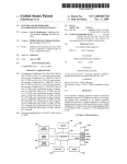
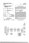
FIG. 1 shows the general con?guration of photocopy
counter and access controller system 10 comprised of
central processor unit (CPU) 12, random access mem
4
amount of time causes a reset command to be issued on
line 96 from power down circuit 20. The power down
circuit will be discussed in detail later.
Thus, CPU 12 communicates with RAM 14 only
after the chip select signal from decoder 22 has been
enabled by power down circuit 20. On the other hand,
no chip decoding is necessary when CPU 12 communi
cates with ROM 16. The program ROM is read by CPU
12 by way of data bus 23 and addressed by address bus
21, whenever it has been enabled by control line 11.
Since there is only one program ROM, no decoding is
necessary.
ory (RAM) 14, read only memory (ROM) 16, address
It will be understood that CPU 12 may be a single
latch 18, decoder 22, input/output (I/O) control 24,
chip microcomputer, such as the 8031 microcomputer
power down circuit 20, serial port 26, copier interface
circuit 28, and I/O subsystem 10a. As shown, I/O sub
system 10a contains keyboard 42, display 50, user opera
tor switch 44, and badge reader 54. All communications
between the I/O subsystem and the CPU are done by
way of I/O control 24. U0 subsystem 10a also contains
which has capability of accessing memory and I/O
2764 chip for storing the program. The RAM consists
keyboard scan decoder and driver 40, character de
dress space. The ?rst two are blocks of CMOS battery
coder 45, display driver 48, and segment driver 52.
CPU 12 is the “brains” of the system. All program
execution is performed within it. While the program is
executed within the CPU, it is actually stored in ROM
16 and the CPU fetches each instruction to be executed
from ROM 16. Aside from program instructions, there
is also data to be manipulated and stored. As in program
execution, all data manipulation (for example, add, sub
tract, compare, etc.) is performed in CPU 12 but stored
in and read from RAM 14. Besides program instruction
and data, there is also I/O commands and data to be
controlled. The CPU reads and writes data and com
outside of the 8031. The ROM may be a 2716 or 2732 or
of 2048 bytes of memory for data storage and may be
comprised of 5514 or 6514 components. There are three
separate blocks which may be accessed in the data ad
backed-up RAM each being a 1,024 byte block. The
RAM, however, requires decoding by decoder 22,
which may be one chip such as the 74L OO decoder.
Finally, address latch 18 may be a 74LS373 latch for
latching address bits from data bus 23.
Also shown in FIG. 1 is copier interface circuit 28
which is the means by which CPU 12 may control an
30 external device, such as a photocopier (not shown). It
will be understood that copier interface circuit 28 is of
a conventional type and may be similar to the interface
circuit disclosed by the Danyl System 80, User Manual
which is incorporated herein by reference. The general
mands from and to I/O subsystem 10a by way of I/O
control 24.
35 con?guration of badge reader 54 is also disclosed
To allow CPU 12 to access RAM 14, ROM 16, or
I/O control 24, the CPU places the ?rst portion of an
address in address latch 18 by way of data bus 23, and
the second portion of the address is placed directly onto
address bus 21. The ?rst portion of the address is
therein. Control signals are sent from CPU 12 to copier
interface circuit 28 by way of line 27. Such control
signal may be an on/off message from CPU 12 which
corresponds to an enable/ disable state on line 19 for the
photocopier being controlled.
latched, when an address latch enable is placed on line
External events, such as copy pulses, also may be
13. After the latching of the ?rst portion of the address,
interfaced and counted by way of copier interface cir
cuit 28. It will be understood that such copy pulses are
data bus 23 is used for data transmission or reception.
generated by photocopying devices for purpose of
The output of address latch 18 is decoded by decoder
22 in order to select the proper chip in RAM 14 by way 45 maintaining counts of the number of photocopies made
of chip select line 92. As shown, the chip selects ?rst go
by such devices. Since the signal characteristics of the
through power down circuit 20 by way ofline 83 so that
the data in the RAM may be protected when system
power is off, or when power is being cycled on or off.
If power down circuit 20 senses proper voltage condi
copy pulses are different from one photocopier to an
tions, it will permit chip selection in RAM 14. Once
permitted, data may be read from or written to the
selected address in RAM 14 by way of data bus 23.
The power down circuit also provides other func
tions. It contains a battery backup for the RAM and
supplies backup power by way of line 94. In addition, it
generates several signals to CPU 12. One such signal
placed on line 67, is an advanced warning that system
power is being shut down. Another signal, placed on
line 100, is a warning that the battery power is low and,
therefore, the battery should be replaced. Still another
other, copier interface circuit 28 may accommodate
various types of inputs from the photocopy devices.
Such inputs, for example. may be l20 VAC, 24 VDC
and 5 VDC. The time duration of these pulse inputs
may also be of various lengths, for example, they may
vary from a few milliseconds to few tenths of seconds.
When a copy pulse is detected on line 19 by the copier
interface circuit, the pulse is placed on line 27 for fur
ther timing and evaluation by CPU 12. The timing and
evaluation performed by CPU 12 on the copy pulses
will be explained in detail later.
CPU 12 may also communicate with other peripheral
devices (not shown) by way of serial port 26. It will be
understood that serial port 26 is of a conventional type
and may be an RS422 port. Such port permits periph
the CPU whenever power comes on or off and when
eral devices to control system 10, maintain the system,
ever a program malfunction is detected.
and pass data to and from the system.
Another function of power down circuit 20 is to 65
Still referring to FIG. 1, there is shown I/O control
monitor CPU 12 activity. A signal, placed on line 87, is
24. CPU 12 communicates with U0 subsystem 100
signal, placed on line 96, provides a reset command to
issued by CPU 12 indicating that the program is running
correctly. Failure to issue this signal within a certain
through I/O control 24 by way of keyboard data bus 41,
U0 address bus 43, U0 data bus 47 and blanking 45. It