1
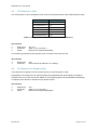
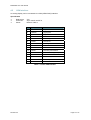
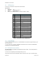
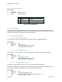
MODBASE 210
BASE BOARD FOR COM EXPRESS MODULES
USER MANUAL
Revision 0.2
MODBASE 210 User Manual
Revision
Revision
Changes
Date / Name
0.2
First Edition
08.11.06 dh
DISCLAIMER
Copyright
© 2006 ELTEC Elektronik AG. The information, data, and figures in this document including respective
references have been verified and found to be legitimate. In particular in the event of error they may,
therefore, be changed at any time without prior notice. The complete risk inherent in the utilization of
this document or in the results of its utilization shall be with the user; to this end, ELTEC Elektronik AG
shall not accept any liability. Regardless of the applicability of respective copyrights, no portion of this
document shall be copied, forwarded or stored in a data reception system or entered into such
systems without the express prior written consent of ELTEC Elektronik AG, regardless of how such
acts are performed and what system is used (electronic, mechanic, photocopying, recording, etc.). All
product and company names are registered trademarks of the respective companies.
Our General Business, Delivery, Offer, and Payment Terms and Conditions shall otherwise apply.
Federal communications commission statement
a
a
a
a
a
a
a
a
a
This device complies with FCC Rules Part 15. Operation is subject to the following two
conditions:
This device may not cause harmful interference, and
This device must accept any interference received including interference that may cause
undesired operation.
This equipment has been tested and found to comply with the limits for a Class B digital
device, pursuant to Part 15 of the FCC Rules. These limits are designed to provide reasonable
protection against harmful interference in a residential installation. This equipment generates,
uses and can radiate radio frequency energy and, if not installed and used in accordance with
manufacturer’s instructions, may cause harmful interference to radio communications.
However, there is no guarantee that interference will not occur in a particular installation. If this
equipment does cause harmful interference to radio or television reception, which can be
determined by turning the equipment off and on, the user is encouraged to try correct the
interference by one or more of the following measures:
Reorient or relocate the receiving antenna.
Increase the separation between the equipment and receiver.
Connect the equipment to an outlet on a circuit different from that to which the receiver is
connected.
Consult the dealer or an experienced radio/TV technician for help.
The us of shielded cables for connection of the monitor to the graphics card is required to
assure compliance with FCC regulations. Changes or modifications to this unit not expressly
approved by the party responsible for compliance could void the user’s authority to operate
this equipment.
Canadian department of communications statement
a
a
This digital apparatus does not exceed the Class B limits for radio noise emissions from digital
apparatus set out in the Radio Interference Regulations of the Canadian Department of
Communications.
This class B digital apparatus complies with Canadian ICES-003
Revision 0.2
2|2
MODBASE 210 User Manual
SAFETY INFORMATION
Electrical safety
a
a
a
a
a
To prevent electrical shock hazard, disconnect the power cable from the electrical outlet
before reloading the system.
When adding or removing devices to or from the system, ensure that the power cables for the
devices are unplugged before the signal cables are connected. If possible, disconnect all
power cables from the existing system before you add device.
Before connecting or removing signals cables from motherboard, ensure that all power cables
are unplugged.
Make sure that your power supply is set to the correct voltage in your area. If you are not sure
about the voltage of the electrical outlet you are using, contact your local power company.
If the power supply is broken, do not try to fix it by yourself. Contact a qualified service
technician or your retailer.
Operation safety
a
a
a
a
a
a
Before installing the motherboard and adding devices on it, carefully read the manuals that
came with the package.
Before using the product, make sure all cables are correctly connected and the power cables
are not damaged. If you detect any damage, contact your dealer immediately.
To avoid short circuits, keep paper clips, screws, and staples away from connectors, slots
sockets and circuitry.
Avoid dust, humidity, and temperature extremes. Do not place the product in any area where it
may become wet.
Place the product on a stable surface.
If you encounter technical problems with the product, contact a qualified service technician or
your retailer.
EMC Rules
This unit has to be installed in a shielded housing. If not installed in a properly shielded enclosure, and
used in accordance with the instruction manual, this product may cause radio interference in which
case the user may be required to take adequate measures at his or her own expense.
IMPROTANT INFORMATION
This product is not an end user product. It was developed and manufactured for further processing by
trained personnel.
RECYCLING
Please recycle packaging environmentally friendly:
Packaging materials are recyclable. Please do not dispose packaging into domestic waste but
recycle it.
Please recycle old or redundant devices environmentally friendly:
Old devices contain valuable recyclable materials that should be reutilized. Therefore please
dispose old devices at collection points which are suitable.
Revision 0.2
3|3
MODBASE 210 User Manual
TABLE OF CONTENTS
MODBASE 210 ....................................................................................................................................... 1
1 General ............................................................................................................................................ 6
1.1
Revisions and Modifications ......................................................................................................... 6
1.2
Reference Documents.................................................................................................................. 6
1.3
Definitions and Abbreviations ....................................................................................................... 7
2 Introduction .................................................................................................................................... 8
2.1
Product Description ...................................................................................................................... 8
2.2
Block Diagram .............................................................................................................................. 9
2.3
Positioning of the Connectors..................................................................................................... 10
3 Mechanics ..................................................................................................................................... 11
3.1
Dimensions ................................................................................................................................. 11
4 Hardware ....................................................................................................................................... 12
4.1
Plug-in Position of the COM Express module ............................................................................ 12
4.2
PCI Slots..................................................................................................................................... 12
4.3
PCI Express x1 Slots.................................................................................................................. 13
4.4
PCI Express x16 Graphics Slot .................................................................................................. 13
4.5
VGA Interface ............................................................................................................................. 14
4.6
LVDS-Interface ........................................................................................................................... 15
4.6.1
LVDS EEPROM ............................................................................................................... 15
4.6.2
Backlight Inverter Interface .............................................................................................. 15
4.7
JILI Interface ............................................................................................................................... 16
4.7.1
Standard JILI Connector.................................................................................................. 16
4.7.2
JILI40 Connector ............................................................................................................. 16
4.8
TV Out ........................................................................................................................................ 17
4.9
Audio........................................................................................................................................... 17
4.9.1
Mono-Microphone............................................................................................................ 18
4.9.2
Stereo LineIn.................................................................................................................... 18
4.9.3
Stereo LineOut................................................................................................................. 18
4.9.4
Stereo Headphone........................................................................................................... 19
4.10
IDE Interface ........................................................................................................................... 19
4.10.1 Primary IDE Channel ....................................................................................................... 19
4.11
SATA-Interface ....................................................................................................................... 20
4.12
USB Topology......................................................................................................................... 20
4.12.1 USB Power Supply .......................................................................................................... 21
4.13
Ethernet................................................................................................................................... 21
4.14
LPC Slot .................................................................................................................................. 22
4.15
I/O Connector.......................................................................................................................... 23
4.16
GPIO ....................................................................................................................................... 23
4.17
ATX Connector ....................................................................................................................... 24
4.18
SuperIO................................................................................................................................... 24
4.18.1 COM Ports ....................................................................................................................... 24
4.18.2 IrDA.................................................................................................................................. 25
4.18.3 PS/2 ................................................................................................................................. 26
4.18.4 Fan interface .................................................................................................................... 26
4.18.5 SuperIO Hardware Monitor.............................................................................................. 27
4.19
SMB Hardware Monitor........................................................................................................... 27
4.20
Serial EEPROM at SMBus...................................................................................................... 27
4.21
Serial EEPROM at I2C-Bus .................................................................................................... 27
4.22
OnBoard BIOS-Flash .............................................................................................................. 28
4.23
POST-Code Display................................................................................................................ 28
4.23.1 Lattice Programming Interface......................................................................................... 29
4.24
Battery..................................................................................................................................... 29
4.25
Beeper..................................................................................................................................... 29
4.26
Power Button .......................................................................................................................... 29
Revision 0.2
Page 4 of 4
MODBASE 210 User Manual
4.27
4.28
Reset of the System................................................................................................................ 30
Miscellaneous ......................................................................................................................... 30
4.28.1 Measuring Resistors for current measuring..................................................................... 30
4.28.2 Ground Pins ..................................................................................................................... 30
4.28.3 Sleep State LED Display ................................................................................................. 30
ILLUSTRATIONS
Illustration 1 Block Diagram Main Board ............................................................................................... 9
Illustration 2 Positioning of the Connectors ......................................................................................... 10
TABLES
Table 1 Assignment PCI slot to connector reference.......................................................................... 12
Table 2 Assignment PCI Express Lane to connector reference ......................................................... 13
Table 3 Pinout VGA Interface.............................................................................................................. 14
Table 4 Pinout Single Channel LVDS-Interface .................................................................................. 15
Table 5 Pinout Backlight...................................................................................................................... 16
Table 6 Pinout TV-Out......................................................................................................................... 17
Table 7 Pinout TV-Out Pin header ...................................................................................................... 17
Table 8 Pinout Microphone.................................................................................................................. 18
Table 9 Pinout LineIn........................................................................................................................... 18
Table 10 Pinout LineOut...................................................................................................................... 18
Table 11 Pinout Headphone................................................................................................................ 19
Table 12 Assignment SATA Channel to Connector Reference .......................................................... 20
Table 13 Assignment USB Ports......................................................................................................... 20
Table 14 Pinout LPC-Slot .................................................................................................................... 22
Table 15 Pinout I/O-Connector............................................................................................................ 23
Table 16 Pinout GPIO connector ........................................................................................................ 24
Table 17 Assignment COM Ports to Connector Reference ................................................................ 25
Table 18 Pinout COM Ports ................................................................................................................ 25
Table 19 Pinout IrDA ........................................................................................................................... 25
Table 20 Pinout Upper PS/2 Jack ....................................................................................................... 26
Table 21 Pinout Lower PS/2 Jack ....................................................................................................... 26
Table 22 Pinout Fan Interface ............................................................................................................. 26
Table 23 Pinout POST Display (HP-POD) .......................................................................................... 28
Table 24 Pinout Lattice Programming Interface.................................................................................. 29
Revision 0.2
Page 5 of 5
MODBASE 210 User Manual
1
General
1.1
Revisions and Modifications
Revision
Date
Author
Comment
0.1
03.08.2006
USte
Generated, German version
0.2
08.11.2006
bkae, kol
Translated to English
1.2
Reference Documents
[1] COM Express Module Base Specification
COM Express Revision 1.0
Last update: July 10th, 2005
[2] ATX Specification
atx2_21.pdf
Version 2.2
http://www.formfactors.org
[3] PCI Local Bus Specification Rev. 2.1
PCI21.PDF
Last update: June 1st, 1995
http://www.pcisig.com
[4] JILI Specification
Jilim120.pdf
Last update: April 7th, 2003
http://www.jumptec.de/product/data/jili/index.html
[5] Digital Video Interface DVI
dvi_10.pdf
Rev. 1.0 April 2nd, 1999
http://www.ddwg.org/
[6] ATA/ATAPI-6 Specification
d1410r3b.pdf
http://www.t13.org/
[7] CF+ & CF Specification Rev. 3.0
cfspc3_0.pdf
http://www.compactflash.org/
[8] Serial ATA Specification
Serial ATA 1.0 gold.pdf
Last update: August 29th, 2002 Rev.1.0
http://www.sata-io.org/
[9] IEEE Std. 802.3-2002
802.3-2002.pdf
http://www.ieee.org
[10] Universal Bus Specification
usb_20.pdf
Last update: April 27th, 2000
http://www.usb.org
Revision 0.2
Page 6 of 6
MODBASE 210 User Manual
1.3
Definitions and Abbreviations
COM
RTC
ATX
PCI
IDE
EIDE
CF
ATA
ATAPI
SATA
USB
PEG
GPIO
LVDS
JILI
LAN
VGA
LPC
POST
SMBus
MDI
Revision 0.2
Computer-On-Module
Real Time Clock
Advanced Technology Extended
Peripheral Component Interconnect
Integrated Drive Electronics
Enhanced Integrated Drive Electronics
Compact Flash
Advanced Technology Attachment
Advanced Technology Attachment with Packet Interface
Serial Advanced Technology Attachment
Universal Serial Bus
PCI express Graphics
General Purpose Input / Output
Low Voltage Differential Signaling
JUMPtec Intelligent LVDS Interface
Local Area Network
Video Graphics Array
Low Pin Count
Power on self test
System Management Bus
Medium Dependent Interface
Page 7 of 7
MODBASE 210 User Manual
2
Introduction
2.1
Product Description
COM Express modules are compact, highly integrated Single Board Computers.
Typically a COM Express module consists of CPU, chipset, memory, video controller, Ethernet
controller, BIOS flash and EIDE-, SATA- and USB controller. Interface controllers (e.g. for PCMCIA) or
connectors (e.g. RJ45) are implemented on the base board on to which the COM Express module can
be mounted via one or two 220-pin SMD-connectors. Beside the power supply also signals for PCI
Express- and PCI-bus, EIDE, SATA, USAB, LPC etc. are present on these connectors.
The type of interfaces that is led from the COM Express module to the base board depends on the
type of module that is used. The COM Express specification defines five different types which differ in
number and pin assignment of the module connectors.
Thanks to the standardized mechanics and interfaces the system can be scaled arbitrarily. Despite a
modular concept the systems design is very flat and compact.
COM Express modules need a base-board for successful operation.
The main board described in the following acts as an evaluation board for the modules.
Features
a
a
a
a
a
a
a
a
a
a
a
a
a
a
a
a
a
a
a
a
a
a
a
a
Interface for COM Express module type 2 up to extended form factor
4 PCI slots 32Bit v2.1
6 PCI Express slots
PCI Express x16 graphics / SDVO
VGA interface
LVDS interface
Standard JILI / JILI40
TV-Out
AC'97-Link
" LineIn
" LineOut
" Headphone
" Microphone
40 pin IDE interface Ultra ATA-100/66/33
44 pin IDE interface Ultra ATA-100/66/33
Compact flash interface Spec. v3.0
4 SATA channels up to 150MB/s
8 USB2.0 root hub interfaces
LAN interface max. 1GBit
LPC slot
Pin header for GPIOs
SuperIO W83627THF
" 2x PS/2
" 2x COM
" 1x IrDA
" 2 fan interfaces
" Hardware monitoring
Power supply via ATX connector
POST display on LPC
Serial EEPROM on I²C-Bus
Serial EEPROM on SMBus
On-board BIOS Flash
Beeper
Revision 0.2
Page 8 of 8
Revision 0.2
PS/2
COM1
COM2
SMB
IO
Stecker
PS/2
Erweiterungskarte
LPC-Slot
Port80h
GPIO
GPIO
COM1
LPC
COM2
IrDA
SuperIO
I²C
EEPROM
HW
Monitor
MDI
HW
Monitor
EEPROM
Lüfter
Mic
AC-Link
AC97-Codec
LineOut
SMB
4x
PCI-Slot
PCI
6
PCIe
TV-out
TV-out
6x
PCIe-Slot
Kopfhörer
COM Expressmodul
LineIn
8x
USB
8
USB
VGA
VGA
A B
LVDS
4x
SATA
4
SATA
PCIe-G
PCIe
Graphics
IDE
LVDS-I²C
JILI
EEPROM
std. JILI
JILI40
LCD
CF
Slot
44pol.
Stecker
40pol.
Stecker
Backlight
2.2
Übertrager
LAN
MODBASE 210 User Manual
Block Diagram
Illustration 1 Block Diagram Main Board
Page 9 of 9
MODBASE 210 User Manual
2.3
Positioning of the Connectors
Illustration 2 Positioning of the Connectors
Revision 0.2
Page 10 of 10
MODBASE 210 User Manual
3
Mechanics
3.1
Dimensions
a
a
a
a
Dimension:
Width:
Tolerances of the drill holes:
Tolerances of the diameter:
Revision 0.2
254.5 mm x 36.8 mm
1.6 mm + /-10%
+/- 0.1mm in X and Y
+ 0.1 mm
Page 11 of 11
MODBASE 210 User Manual
4
Hardware
4.1
Plug-in Position of the COM Express module
A plug-in for COM Express type 2 modules is available on the main board.
Following form factors are supported:
a
a
a
Compact module (ELTEC specific format)
Basic module
Extended module
Specification
a
a
Reference:
Connector:
a
Pinout:
4.2
PCI Slots
X1
AMP / Tyco 3-1827233-6
0.5 mm pitch free height 440 pin 5H plug (combination of two 220pin plugs)
Refer to COM Express specification for type 2 module [1]
Four 32-bit PCI slots are provided according to PCI specification v2.1.
The signal assignment:
a
a
a
a
INTA#, INTB#, INTC# and INTD#
REQ[0..3]#
GNT[0..3]#
IDSEL
for slot 0, slot 1, slot 2 and slot 3 is defined in the COM Express specification [1]
PCI Slot
Reference
PCI Slot 0
PCI Slot 1
PCI Slot 2
PCI Slot 3
X2
X3
X4
X5
Table 1 Assignment PCI slot to connector reference
Specification
a
a
a
References:
Connector:
Pinout:
Revision 0.2
X2 - X5
AMP / Tyco 5145154-4
Refer to PCI specification v2.1 [3]
Page 12 of 12
MODBASE 210 User Manual
4.3
PCI Express x1 Slots
One PCI Express x1 slot is assigned to each of the 6 PCI Express lanes of the COM Express module.
PCI Express Lane
References
PCI Express Lane 0
X6
PCI Express Lane 1
X7
PCI Express Lane 2
X8
PCI Express Lane 3
X9
PCI Express Lane 4
X10
PCI Express Lane 5
X11
Table 2 Assignment PCI Express Lane to connector reference
Specification
a
a
a
References:
Connector:
Pinout:
X6 - X11
AMP / Tyco 4-1612163-1
Refer to PCI express specification
For measuring purposes the PCI express clock is routed to test connector X54.
Specification
a
a
References:
Connector:
X54
Huber+Suhne 82 SMA-50-0-1/111NE(H)
4.4
PCI Express x16 Graphics Slot
A PCI Express X16 graphics slot is provided as plug-in for PEG graphics cards.
Depending on the chipset the PCI Express signals are multiplexed with SDVO signals, thus SDVO
modules can be run in this slot as well. SDVO or PCI Express graphics will be activated automatically
via PullUps of the SDVO I²C interface on the SDVO module.
Specification
a
a
a
References:
Connector:
Pinout:
Revision 0.2
X12
AMP / Tyco 4-1612163-4
Refer to PCI express specification
Page 13 of 13
MODBASE 210 User Manual
4.5
VGA Interface
An analog display can be connected via a VGA (VESA DDC) interface.
Specification
a
a
a
References:
Connector:
Pinout:
X13
Suyin 7507S-15G5T-A
Refer to Table 3
Pin
Signal name
Function
1
RED
Signal red
2
GREEN
Signal green
3
BLUE
Signal blue
4
RSVD
reserved
5
GND
Ground digital
6
RGND
Ground red
7
GGND
Ground green
8
BGND
Ground blue
9
+5V
+5V VDC
10
SGND
Ground Synchronisation
11
ID0
Monitor ID Bit 0 (optional)
12
SDA
DDC Data
13
HSYNC
Horizontal Sync.
14
VSYNC
Vertical Sync.
15
SCL
DDC Clock
Table 3 Pinout VGA Interface
Revision 0.2
Page 14 of 14
MODBASE 210 User Manual
4.6
LVDS-Interface
LCDs can be connected via a single channel LVDS interface:
Specification
a
a
a
a
References:
X14
Connector:
Hirose DF19G-20P-1H
Pinout:
Refer to Table 4
Pin 20 can be configured via 0Ohm resistors to “OPEN” or “GND”
Pin
Signal name
Function
1
VDD
Power Supply: +3.3V
2
VDD
Power Supply: +3.3V
3
VSS
Ground
4
VSS
Ground
5
LVDS_A0-
LVDS Negative data signal (-)
6
LVDS_A0+
LVDS Positive data signal (+)
7
VSS
Ground
8
LVDS_A1-
LVDS Negative data signal (-)
9
LVDS_A1+
LVDS Positive data signal (+)
10
VSS
Ground
11
LVDS_A2-
LVDS Negative data signal (-)
12
LVDS_A2+
LVDS Positive data signal (+)
13
VSS
Ground
14
LVDS_A_CK-
LVDS Negative clock signal (-)
15
LVDS_A_CK+
LVDS Positive clock signal (+)
16
VSS
Ground
17
LVDS_A3-
LVDS Negative data signal (-)
18
LVDS_A3+
LVDS Positive data signal (+)
19
VSS
Ground
20
NC / VSS
Reserved / Ground
Table 4 Pinout Single Channel LVDS-Interface
4.6.1 LVDS EEPROM
To store configuration data of the LCD, a serial EEPROM is connected to the signals LVDS_I2C_CK
and LVDS_I2C_DAT.
To avoid conflicts with configuration EEPROMs connected via the JILI connector, this EEPROM is
socketed and can be assembled optionally.
4.6.2 Backlight Inverter Interface
The supply voltage of the backlight can be adjusted with jumper JP0601. The according position is
printed on the PCB.
You have to set J5 depending on the backlight inverter you use.
If the inverter needs a low active start signal, jumper J5 has to be set to L (pin1 connected to pin2).
Revision 0.2
Page 15 of 15
MODBASE 210 User Manual
If the inverter needs a high active start signal, jumper J5 has to be set to H (pin2 connected to pin3).
Brightness of the backlight inverter is controlled via the LVDS-BKLT-CTRL signal.
As the LVDS-BKLT-CTRL signal of the COM Express module is supplied as PWM signal by actual
chipsets, this signal initially is integrated and then limited to the maximum allowable voltage of the
backlight inverter via voltage divider.
Control voltage: 0...3V
A value of 0V corresponds to maximum brightness.
Specification
a
a
a
References:
Connector:
Pinout:
X15
Molex (53047-0510) 53261-0590
Refer to Table 5
Pin
Signal name
Function
1
VCC
Power supply backlight
2
GND
Ground
3
BLON#
Backlight On
4
VCON
Brightness control
5
GND
Ground
Table 5 Pinout Backlight
4.7
JILI Interface
4.7.1 Standard JILI Connector
A standard JILI connector can be used alternatively for connection of LCDs.
Both, single and dual channel LCDs, can be adapted to the main board via small additional PCBs.
Specification
a
a
a
References:
Connector:
Pinout:
X16
Hirose FH12-40S-0.5SV
"standard JILI" according to JILI specification [4]
4.7.2 JILI40 Connector
Any LCD display can be adapted via a JILI40 connector.
Two 24 bit LVDS channels are present on this 40-pin header
Specification
a
a
a
References:
Connector:
Pinout:
Revision 0.2
X46
Samtec TMM-120-01-LM-D-SM-P
"JILI40" according to JILI specification [4]
Page 16 of 16
MODBASE 210 User Manual
4.8
TV Out
A TV-OUT connector is implemented for displaying the video signal on a TV set (or the like). The main
board supports the following video signals
a
Composite Video
a
Component Video (YPbPr)
a
S-Video
The type of the video signal is defined by the graphics controller on the COM Express module.
Specification
a
a
a
References:
Connector:
Pinout:
X17
AMP 5786766-1
Refer to Table 6
Pin
Signal name
Composite
Component
S-Video
1
TV_IRTN_B
Ground
Ground
Ground
2
TV_IRTN_C
Ground
Ground
Ground
3
TV_DACB
not used
Luminance (Y)
Luminance
4
TV_DACC
not used
Chrominance (Pr)
Chrominance
5
TV_DACA
CVBS
Chrominance (Pb)
not used
6
TV_IRTNA
Ground
Ground
Ground
7
RSVD
reserved
reserved
reserved
Table 6 Pinout TV-Out
The signals can be adapted to another connector with a 10-pin header.
Specification
a
a
a
References:
Connector:
Pinout:
X53
IDC-M 10pol. THT RM2.54
Refer to Table 7
Pin
Signal
Pin
Signal
1
GND
2
TV_DACA
3
GND
4
TV_DACB
5
GND
6
TV_DACC
7
GND
8
GND
9
GND
10
GND
Table 7 Pinout TV-Out Pin header
4.9
Audio
An AC’97 codec V2.2 is connected to the AC link of the COM Express module. Footprint and circuit
are compatible to following AC’97 codecs:
a
a
VIA VT1612A
Realtek ALC650
Revision 0.2
Page 17 of 17
MODBASE 210 User Manual
Following NF signals are provided by the AC’97 codec:
a
a
a
a
Mono Microphone
Stereo LineIn
Stereo LineOut
Stereo Headphone
4.9.1 Mono-Microphone
Bias voltage for capactior microphones is provided.
Specification
a
a
a
References:
Connector:
Pinout:
X18
Kycon ST-3000
Refer to Table 8
Pin
Signal name
Function
1
GND
Ground
2
MIC_BIAS
Bias initial load (ring)
3
MIC
NF signal (tip)
Table 8 Pinout Microphone
4.9.2 Stereo LineIn
Specification
a
a
a
References:
Connector:
Pinout:
X19
Kycon ST-3000
Refer to Table 9
Pin
Signal name
Function
1
GND
Ground
2
LINEIN_R
NF signal right (ring)
3
LINEIN_L
NF signal left (tip)
Table 9 Pinout LineIn
4.9.3 Stereo LineOut
Specification
a
a
a
References:
Connector:
Pinout:
X20
Kycon ST-3000
Refer to Table 10
Pin
Signal name
Function
1
GND
Ground
2
LINEOUT_R
NF signal right (ring)
3
LINEOUT_L
NF signal left (tip)
Table 10 Pinout LineOut
Revision 0.2
Page 18 of 18
MODBASE 210 User Manual
4.9.4 Stereo Headphone
Specification
a
a
a
References:
Connector:
Pinout:
X21
Kycon ST-3000
Refer to Table 11
Pin
Signal name
Function
1
GND
Ground
2
HPOUT_R
NF signal right (ring)
3
HPOUT_L
NF signal left (tip)
Table 11 Pinout Headphone
4.10
IDE Interface
A standard IDE interface is provided according to ATA/ATAPI, with the controller supporting at least
Ultra-ATA100 with 100 MB/sec data rate. The transfer mode that can be selected depends on how the
system is wired and which modes are supported by the drives.
4.10.1 Primary IDE Channel
4.10.1.1 40-pin IDE interface
A 40-pin IDC connector is provided at the primary IDE channel for standard IDE drives.
Specification
a
a
References:
Connector:
Pinout:
X22
FCI 75869-118
Refer to Specification ATA/ATAPI-6
Source [6], page 400, Table A3
4.10.1.2 44-pin IDE Interface
For connection of 2.5” hard disks, a 44-pin IDC connector is provided at the primary IDE channel.
Specification
a
a
a
References:
Connector:
Pinout:
X23
Yamaichi ZP7-44-S-G
Refer to Specification ATA/ATAPI-6
Source [6], page 412, Table A16
4.10.1.3 Compact Flash Interface
A socket for compact flash cards, type I/II, is provided at the primary IDE channel.
The compact flash interface supports True IDE mode according to compact flash specification rev. 3.0.
Inter alia the compact flash specification rev. 3.0 supports the UDMA mode.
Specification
a
a
a
References:
Connector:
Pinout:
Revision 0.2
X24
Yamaichi CF050P2-003-10-D2
Refer to specification "CF+ & CF specification rev. 3.0"
Source [7] , page 24, table 4
Page 19 of 19
MODBASE 210 User Manual
4.11
SATA-Interface
For SATA drives four connectors are populated with SATA interface (signals + power).
Every SATA signal connector has its own power supply connector.
SATA Channel
References
SATA 0
X25
SATA 1
X26
SATA 2
X27
SATA 3
X28
Table 12 Assignment SATA Channel to Connector Reference
Specification SATA signal connector
a
a
a
References:
Connector:
Pinout:
X25 - X28
Molex 87713 series
Refer to Specification SATA
Source [8], page 46, table 3
Specification Power Supply
a
a
a
References:
Connector:
Pinout:
X49 - X52
AMP 171825-4
Refer to ATX specification v2.2 [2]; "Floppy Drive Power Connector"
4.12
USB Topology
Eight USB ports are provided by the COM Express module.
The exact assignment of each port is defined in the following table:
USB-Port
References
Description
USB0
X29
External dual connector 1
USB1
X29
External dual connector 1
USB2
X30
External dual connector 2
USB3
X30
External dual connector 2
USB4
X31
External dual connector 3
USB5
X31
External dual connector 3
USB6
X32
External dual connector 4
USB7
X32
External dual connector 4
Table 13 Assignment USB Ports
Revision 0.2
Page 20 of 20
MODBASE 210 User Manual
4.12.1 USB Power Supply
The power supplies are protected by USB power switches. In addition to that the input voltages of the
USB power switches are protected by resetable fuses.
The USB power switches have the following functions:
a
a
a
a
a
a
The output current is limited to 500mA per port
A signal to detect overcurrent is generated for each two ports
USB0 and USB1 have one common signal to detect overcurrent
USB2 and USB3 have one common signal to detect overcurrent
USB4 and USB5 have one common signal to detect overcurrent
USB6 and USB7 have one common signal to detect overcurrent
Specification
a
a
a
References:
Connector:
Pinout:
4.13
Ethernet
X29 - X32
AMP 787617-2 (Dual USB connector type A)
according to USB specification 2.0 [10]
The mainboard can be connected to a local area network with an ethernet interface.
The COM Express module already provides MDI signals, so that there is only the transformer on the
mainboard required.
The transformer PULSE H 5004 not only supports 10BaseT and 100BaseTX but also 1Gbit.
Specification
a
a
a
References:
Connector:
Pinout:
Revision 0.2
X33
AMP 2-406549
Refer to IEEE Std. 802.3 [9], section three, page 225
Page 21 of 21
MODBASE 210 User Manual
4.14
LPC Slot
You have an LPC slot available to insert extension board with LPC interface.
Specification
a
a
a
References:
Connector:
Pinout:
X34
36-pin header, 2.54mm
Refer to Table 14
Pin
Signal
Pin
Signal
1
VCC5V
2
VCC5V
3
NC
4
VCC3V3
5
VCC3V3
6
NC
7
VCC3V3_SBY
8
GND
9
GND
10
LPC_RST#
11
GND
12
LPC_LAD0
13
LPC_LAD1
14
LPC_LAD2
15
LPC_LAD3
16
LPC_FRAME#
17
GND
18
LPC_DRQ0
19
GND
20
LPC_CLK
21
GND
22
LPC_PWRDWN
23
GND
24
PME#
25
GND
26
LPC_SMI#
27
GND
28
SERIRQ
29
GND
30
PCI_CLKRUN#
31
GND
32
CPU_RST#
33
GND
34
LPC_DRQ1#
35
GND
36
GND
Table 14 Pinout LPC-Slot
Revision 0.2
Page 22 of 22
MODBASE 210 User Manual
4.15
I/O Connector
An alternative SuperIO controller can be integrated via a 36-pin connector. In this case the onboard
chip is not populated and a piggy back board with the SuperIO chip is plugged into the I/O and into the
LPC connector.
Specification
a
a
a
References:
Connector:
Pinout:
X45
CAB 1002-161-036
Refer to Table 15
Pin
1
3
5
7
9
11
13
15
17
19
21
23
25
27
29
31
33
35
Signal
SMB_CLK
SMB_DAT
KBDAT
KBCLK
MSDAT
MSCLK
NC
NC
NC
NC
COM1_DCD#
COM1_RXD
COM1_TXD
COM1_DTR#
COM1_DSR#
COM1_RTS#
COM1_CTS#
COM1_RI#
Pin
2
4
6
8
10
12
14
16
18
20
22
24
26
28
30
32
34
36
Signal
SLP_S3#
SLP_S4#
SLP_S5#
EXT_THRM#
SMBALERT#
NC
THRMTRIP#
BATLOW#
NC
NC
COM2_DCD#
COM2_RXD
COM2_TXD
COM2_DTR#
COM2_DSR#
COM2_RTS#
COM2_CTS#
COM2_RI#
Table 15 Pinout I/O-Connector
4.16
GPIO
The COM Express module provides four general purpose outputs and four general purpose inputs.
The GPIs have PullUp resistors and are routed to a dip switch (SW1103). With the dip switch the GPIs
can be connected to ground. The assignment GPI – switch – level is printed on the PCB.
If the PullUp resistors are not populated, you can switch LPC_SMI# or HWM_SMI# to GPI0, GPI1,
GPI2 or GPI3 with jumper JP1101.
The GPOs are connected to LEDs to optically display the status.
Revision 0.2
Page 23 of 23
MODBASE 210 User Manual
Specification
a
a
a
References:
Connector:
Pinout:
X35
CAB 1002-161-036
Refer to Table 16
Pin
Signal
Pin
Signal
1
GPI0
2
GND
3
GPI1
4
GND
5
GPI2
6
GND
7
GPI3
8
GND
9
GPO0
10
GND
11
GPO1
12
GND
13
GPO2
14
GND
15
GPO3
16
GND
Table 16 Pinout GPIO connector
4.17
ATX Connector
An ATX connector with additional ATX12V connector is available for power supply of the system.
Specification ATX connector
a
a
a
References:
Connector:
Pinout:
X36
Molex 44206-0007
Refer to ATX specification v2.2 [2]
Specification ATX12V connector
a
a
a
References:
Connector:
Pinout:
4.18
SuperIO
X37
Molex 39-29-9042
Refer to ATX specification v2.2 [2]
The Winbond SuperIO W83627THF is integrated on the base board.
Interfaces used by the SuperIO
a
2 RS232 interface (function of COM port shared with IrDA interface)
a
1 IrDA interface (function shared with COM port)
a
PS/2 interface for keyboard and mouse
a
2 fan interfaces
a
4 voltage control
a
1 temperature control
4.18.1 COM Ports
Characteristics of the COM ports
a
a
a
RS232 standard
RS232 transceiver ESD protected +/- 15kV
EMC improvement by using EMI filters in the signal lines
Revision 0.2
Page 24 of 24
MODBASE 210 User Manual
The exact assignment of each single port to the connector reference can be seen from the following
table:
COM Port
References
COM 1
X38
COM 2
X39
Table 17 Assignment COM Ports to Connector Reference
Specification
a
a
a
References:
Connector:
Pinout:
X38 and X39
Weitronic 107-091-10-10-10
Refer to Table 18
Pin
Signal name
Function
1
DCD#
Data Carrier Detect
2
RXD
Receive Data
3
TXD
Transmit Data
4
DTR#
Data Terminal Ready
5
GND
Ground
6
DSR#
Data Set Ready
7
RTS#
Request To Send
8
CTS#
Clear To Send
9
RI#
Ring Indicator
Table 18 Pinout COM Ports
4.18.2 IrDA
The connectors of the IrDA interface are designed for commercial IrDA transmitters.
Specification
a
a
a
References:
Connector:
Pinout:
X40
CAB 1001-161-005
Refer to Table 19
Pin
Signal name
Function
1
+5V
Power supply
2
NC
Not connected
3
IRRX
Received data
4
GND
Ground
5
IRTX
Transmission data
Table 19 Pinout IrDA
Revision 0.2
Page 25 of 25
MODBASE 210 User Manual
4.18.3 PS/2
You have a double PS/2 connector for PS/2 keyboards and PS/2 mice. The upper jack only supports
PS/2 mice. The pins of the lower jack provide both, signals for PS/2 keyboards and those for PS/2
mice. Keyboards can be connected directly, mice can only be operated using an according Y-adapter.
Specification
a
a
a
References:
Connector:
Pinout:
X41
Tyco 84376-1
Refer to Table 20 and Table 21
Pin
Signal name
Function
1
MSDAT
Mouse Data
2
NC
not connected
3
GND
Ground
4
+5V
VCC
5
MSCLK
Mouse Clock
6
NC
not connected
Table 20 Pinout Upper PS/2 Jack
Pin
Signal name
Function
1
KBDAT
Keyboard Data
2
MSDAT
Mouse Data
3
GND
Ground
4
+5V
VCC
5
KBCLK
Keyboard Clock
6
MSCLK
Mouse Clock
Table 21 Pinout Lower PS/2 Jack
4.18.4 Fan interface
Two PWM controlled fan interfaces are integrated on the mainboard. They are located near the COM
Express modul.
Evaluation of the tacho signal and control of the revolution speed is done by the SuperIO.
Specification
a
a
a
References:
Connector:
Pinout:
X42 - X43
Molex 22-04-1031
Refer to Table 22
Pin
Signal name
Function
1
GND
Ground
2
PWM
PWM signal
3
TACHO
Tacho signal
Table 22 Pinout Fan Interface
Revision 0.2
Page 26 of 26
MODBASE 210 User Manual
4.18.5 SuperIO Hardware Monitor
You can check different voltages and temperatures on the hardware monitor that is integrated in the
SuperIO.
Monitored voltages
a
a
a
a
VBAT
3.3V
12V
5V
Measured temperatures
a
Ambient temperature
The temperature is measured with a thermistor.
4.19
SMB Hardware Monitor
In addition to the SuperIO hardware monitor you can also connect a SMBus hardware monitor.
This chip enables you to control different voltages, temperatures and revolution speeds in legacy-freedesigns where the SuperIO is not supported.
Hardware monitor:
a
Winbond W83L786R
Controlled voltages
a
a
a
a
VBAT
3.3V
12V
5V
Measured temperatures
a
Ambient temperature
The temperature is measured with a thermistor.
Fan interface
For evaluation and control of the revolution speeds please refer to chapter 4.17.4.
4.20
Serial EEPROM at SMBus
For testing purposes a serial EEPROM (4kBit) is connected to the SMBus. To avoid address conflicts,
the address can be selected with dip switch SW1101.
4.21
Serial EEPROM at I2C-Bus
For testing purposes a serial EEPROM (4kBit) is connected to the I²C bus. To avoid address conflicts,
the address can be selected with dip switch SW1102.
Revision 0.2
Page 27 of 27
MODBASE 210 User Manual
4.22
OnBoard BIOS-Flash
There is a PLCC32 socket on the mother board, where an additional firmware hub can be inserted. To
boot this from firmware hub, the firmware hub on the COM Express module has to be switched off.
4.23
POST-Code Display
For debugging purposes an POST code display is implemented on the main board, thus enabling the
display of BIOS outputs on IO-port 80h and/or Port 90h.
In addition to that these signals are output on a pin header. For protocolling purposes a logic analyser
can be connected here.
The pinout of the output connector X44 corresponds to the pinout of the Hewlett Packard HP-PODs.
Specification
a
a
a
References:
Connector:
Pinout:
X44
20-pin header 2.54mm
Refer to Table 23
Pin
HP-POD
Function
Pin
HP-POD
Function
1
+5V
not used
2
CLK2
LPC_CLK
3
CLK1
not used
4
D15
not used
5
D14
not used
6
D13
Test signal 3
7
D12
Test signal 2
8
D11
Test signal 1
9
D10
Test signal 0
10
D9
not used
11
D8
Strobe
12
D7
Data 7
13
D6
Data 6
14
D5
Data 5
15
D4
Data 4
16
D3
Data 3
17
D2
Data 2
18
D1
Data 1
19
D0
Data 0
20
GND
Ground
Table 23 Pinout POST Display (HP-POD)
Revision 0.2
Page 28 of 28
MODBASE 210 User Manual
4.23.1 Lattice Programming Interface
A connector used to program the PLD to decode the POST codes is implemented. To reprogram the
PLD a Lattice programming adapter is required.
Specification
a
a
a
References:
Connector:
Pinout:
X47
CAB 714-91-164-31-007 (socket)
Refer to Table 24
Pin
Signal name
Function
1
VCC
Power Supply
2
SDO_TDO
Serial Data Out
3
SDI_TDI
Serial Data In
4
ISPEN#
Programming Enable
5
KEY
Keypin
6
MODE_TMS
Programming Mode
7
GND
Ground
8
SCLK_TCK
Serial Clock
Table 24 Pinout Lattice Programming Interface
4.24
Battery
The RTC on the COM Express module is buffered with a socketed battery on the main board.
To be able to clear the CMOS memory, the battery voltage is connected via jumper J1101 to the COM
Express module.
Type of battery:
2032
Battery socket:
Renata SMTU2032-1
4.25
Beeper
A piezo signal generator is implemented for acoustic signals.
Type: Digisound F/DGX05P
4.26
Power Button
For switching the system on a Power push button has been implemented.
The PWR_BTN# signal is low-active and is connected directly to the corresponding pin of the COM
Express module.
Type: C&K JTP-1230F
Revision 0.2
Page 29 of 29
MODBASE 210 User Manual
4.27
Reset of the System
You have a special push button to reset the system.
The RESET# signal is low-active and is connected to the SYS_RESET#- pin of the COM Express
module.
Type: C&K JTP-1230F
4.28
Miscellaneous
4.28.1 Measuring Resistors for current measuring
Measuring resistors are inserted into the power supply lines of the COM Express module, the PCI
express graphics slot as well as into every single PCI slot and into one PCI express x1 slot.
In addition to these resistors there is one jumper each to be able to measure the current using a wire
loop and a clamp meter.
4.28.2 Ground Pins
There are several ground pins all over the main board for connection of measuring instruments.
4.28.3 Sleep State LED Display
The ELTEC MODBASE 210 has 3 LEDs to display the SleepStates.
LED1201 displays status S3
LED1202 displays status S4
LED1203 displays status S5
Revision 0.2
Page 30 of 30