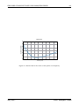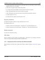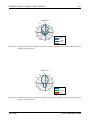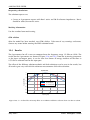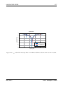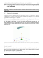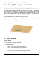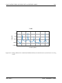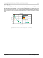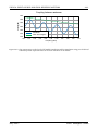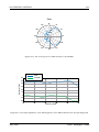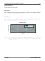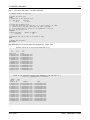
1
ŽŵƉƌĞŚĞŶƐŝǀĞůĞĐƚƌŽŵĂŐŶĞƚŝĐ^ŽůƵƚŝŽŶƐ
FEKO
Examples Guide
Suite 6.1
July 2011
Copyright 1998 – 2011: EM Software & Systems-S.A. (Pty) Ltd
32 Techno Avenue, Technopark, Stellenbosch, 7600, South Africa
Tel: +27-21-880-1880, Fax: +27-21-880-1936
E-Mail: [email protected]
WWW: http://www.feko.info
CONTENTS
i
Contents
Introduction
1
1 Dipole example
1-1
1.1
Dipole . . . . . . . . . . . . . . . . . . . . . . . . . . . . . . . . . . . . . . . . . . . .
1-1
1.2
Results . . . . . . . . . . . . . . . . . . . . . . . . . . . . . . . . . . . . . . . . . . . .
1-2
2 Dipole in front of a cube
2-1
2.1
Dipole and PEC cube . . . . . . . . . . . . . . . . . . . . . . . . . . . . . . . . . . .
2-1
2.2
Dipole and lossy metal cube . . . . . . . . . . . . . . . . . . . . . . . . . . . . . . .
2-2
2.3
Dipole and dielectric cube . . . . . . . . . . . . . . . . . . . . . . . . . . . . . . . .
2-3
2.4
Comparison of the results . . . . . . . . . . . . . . . . . . . . . . . . . . . . . . . .
2-3
3 RCS of a thin dielectric sheet
3-1
3.1
Dielectric sheet . . . . . . . . . . . . . . . . . . . . . . . . . . . . . . . . . . . . . . .
3-1
3.2
Results . . . . . . . . . . . . . . . . . . . . . . . . . . . . . . . . . . . . . . . . . . . .
3-2
4 RCS and near field of a dielectric sphere
4-1
4.1
Dielectric sphere . . . . . . . . . . . . . . . . . . . . . . . . . . . . . . . . . . . . . .
4-1
4.2
Results . . . . . . . . . . . . . . . . . . . . . . . . . . . . . . . . . . . . . . . . . . . .
4-2
5 Shielding factor of a sphere with finite conductivity
5-1
5.1
Finite conductivity sphere (Method of Moments) . . . . . . . . . . . . . . . . . .
5-1
5.2
Finite conductivity sphere (Finite Element Method) . . . . . . . . . . . . . . . .
5-2
5.3
Results . . . . . . . . . . . . . . . . . . . . . . . . . . . . . . . . . . . . . . . . . . . .
5-4
6 Exposure of muscle tissue using MoM/FEM hybrid
6-1
6.1
Dipole and muscle tissue . . . . . . . . . . . . . . . . . . . . . . . . . . . . . . . . .
6-1
6.2
Results . . . . . . . . . . . . . . . . . . . . . . . . . . . . . . . . . . . . . . . . . . . .
6-2
7 A monopole antenna on a finite ground plane
7-1
7.1
Monopole on a finite ground . . . . . . . . . . . . . . . . . . . . . . . . . . . . . .
7-1
7.2
Results . . . . . . . . . . . . . . . . . . . . . . . . . . . . . . . . . . . . . . . . . . . .
7-2
8 Yagi-Uda antenna above a real ground
8-1
8.1
Antenna and ground plane . . . . . . . . . . . . . . . . . . . . . . . . . . . . . . . .
8-1
8.2
Results . . . . . . . . . . . . . . . . . . . . . . . . . . . . . . . . . . . . . . . . . . . .
8-3
9 Pattern optimisation of a Yagi-Uda antenna
9-1
9.1
The antenna . . . . . . . . . . . . . . . . . . . . . . . . . . . . . . . . . . . . . . . .
9-1
9.2
Results . . . . . . . . . . . . . . . . . . . . . . . . . . . . . . . . . . . . . . . . . . . .
9-3
July 2011
FEKO Examples Guide
CONTENTS
ii
10 Microstrip patch antenna
10-1
10.1 Pin-fed, SEP model . . . . . . . . . . . . . . . . . . . . . . . . . . . . . . . . . . . .
10-1
10.2 Pin-fed, planar multilayer substrate . . . . . . . . . . . . . . . . . . . . . . . . . .
10-3
10.3 Edge-fed, planar multilayer substrate . . . . . . . . . . . . . . . . . . . . . . . . .
10-4
10.4 Comparison of the results for the different models . . . . . . . . . . . . . . . . .
10-5
11 Proximity coupled patch antenna with microstrip feed
11-1
11.1 Circular patch . . . . . . . . . . . . . . . . . . . . . . . . . . . . . . . . . . . . . . .
11-1
11.2 Results . . . . . . . . . . . . . . . . . . . . . . . . . . . . . . . . . . . . . . . . . . . .
11-2
12 Dielectric resonator antenna on finite ground
12-1
12.1 DRA fed with a FEM modal port . . . . . . . . . . . . . . . . . . . . . . . . . . . .
12-1
12.2 DRA fed with a waveguide port . . . . . . . . . . . . . . . . . . . . . . . . . . . . .
12-3
12.3 Results . . . . . . . . . . . . . . . . . . . . . . . . . . . . . . . . . . . . . . . . . . . .
12-5
13 A Forked Dipole antenna
13-1
13.1 Forked dipole model . . . . . . . . . . . . . . . . . . . . . . . . . . . . . . . . . . .
13-1
13.2 Results . . . . . . . . . . . . . . . . . . . . . . . . . . . . . . . . . . . . . . . . . . . .
13-2
14 Different ways to feed a horn antenna
14-1
14.1 Wire feed . . . . . . . . . . . . . . . . . . . . . . . . . . . . . . . . . . . . . . . . . .
14-2
14.2 Waveguide feed . . . . . . . . . . . . . . . . . . . . . . . . . . . . . . . . . . . . . .
14-4
14.3 Aperture feed . . . . . . . . . . . . . . . . . . . . . . . . . . . . . . . . . . . . . . . .
14-4
14.4 FEM modal port . . . . . . . . . . . . . . . . . . . . . . . . . . . . . . . . . . . . . .
14-5
14.5 Comparison of the results for the different models . . . . . . . . . . . . . . . . .
14-6
15 A Microstrip filter
15-1
15.1 Microstrip filter on a finite substrate (FEM) . . . . . . . . . . . . . . . . . . . . .
15-1
15.2 Microstrip filter on a finite substrate (SEP) . . . . . . . . . . . . . . . . . . . . . .
15-4
15.3 Microstrip filter on an infinite planar multilayer substrate . . . . . . . . . . . .
15-5
15.4 Results . . . . . . . . . . . . . . . . . . . . . . . . . . . . . . . . . . . . . . . . . . . .
15-6
16 Dipole in front of a UTD/GO/PO plate
16-1
16.1 Dipole in front of a large plate . . . . . . . . . . . . . . . . . . . . . . . . . . . . .
16-1
16.2 Dipole and a UTD plate . . . . . . . . . . . . . . . . . . . . . . . . . . . . . . . . . .
16-2
16.3 Dipole and a GO plate . . . . . . . . . . . . . . . . . . . . . . . . . . . . . . . . . .
16-3
16.4 Dipole and a PO plate . . . . . . . . . . . . . . . . . . . . . . . . . . . . . . . . . . .
16-4
16.5 Comparative results . . . . . . . . . . . . . . . . . . . . . . . . . . . . . . . . . . . .
16-4
17 A lens antenna with Geometrical optics (GO) - ray launching
17-1
17.1 Creating the lens model . . . . . . . . . . . . . . . . . . . . . . . . . . . . . . . . .
17-1
17.2 Results . . . . . . . . . . . . . . . . . . . . . . . . . . . . . . . . . . . . . . . . . . . .
17-4
July 2011
FEKO Examples Guide
CONTENTS
iii
18 Calculating field coupling into a shielded cable
18-1
18.1 Dipole and ground . . . . . . . . . . . . . . . . . . . . . . . . . . . . . . . . . . . . .
18-1
18.2 Results . . . . . . . . . . . . . . . . . . . . . . . . . . . . . . . . . . . . . . . . . . . .
18-2
19 A magnetic-field probe
19-1
19.1 Magnetic-field probe . . . . . . . . . . . . . . . . . . . . . . . . . . . . . . . . . . .
19-1
19.2 Results . . . . . . . . . . . . . . . . . . . . . . . . . . . . . . . . . . . . . . . . . . . .
19-2
20 S-parameter coupling in a stepped waveguide section
20-1
20.1 Waveguide step model (MoM) . . . . . . . . . . . . . . . . . . . . . . . . . . . . .
20-1
20.2 Waveguide step model (FEM) . . . . . . . . . . . . . . . . . . . . . . . . . . . . . .
20-3
20.3 Results . . . . . . . . . . . . . . . . . . . . . . . . . . . . . . . . . . . . . . . . . . . .
20-4
21 Using the MLFMM for electrically large models
21-1
21.1 Large trihedral . . . . . . . . . . . . . . . . . . . . . . . . . . . . . . . . . . . . . . .
21-1
21.2 Results . . . . . . . . . . . . . . . . . . . . . . . . . . . . . . . . . . . . . . . . . . . .
21-2
22 Antenna coupling on an electrically large object
22-1
22.1 Helicopter . . . . . . . . . . . . . . . . . . . . . . . . . . . . . . . . . . . . . . . . . .
22-1
22.2 Results . . . . . . . . . . . . . . . . . . . . . . . . . . . . . . . . . . . . . . . . . . . .
22-2
23 Antenna coupling using an ideal receiving antenna
23-1
23.1 The helix antenna in free space . . . . . . . . . . . . . . . . . . . . . . . . . . . . .
23-1
23.2 Using the helix antenna far-field pattern . . . . . . . . . . . . . . . . . . . . . . .
23-3
23.3 The full model . . . . . . . . . . . . . . . . . . . . . . . . . . . . . . . . . . . . . . .
23-4
23.4 Results . . . . . . . . . . . . . . . . . . . . . . . . . . . . . . . . . . . . . . . . . . . .
23-5
24 Using a point source and ideal receiving antenna
24-1
24.1 The horn antenna in free space . . . . . . . . . . . . . . . . . . . . . . . . . . . . .
24-1
24.2 Using the computed horn radiation pattern in a coupling calculation . . . . . .
24-2
24.3 The reference model . . . . . . . . . . . . . . . . . . . . . . . . . . . . . . . . . . .
24-2
24.4 Results . . . . . . . . . . . . . . . . . . . . . . . . . . . . . . . . . . . . . . . . . . . .
24-2
25 Horn feeding a large reflector
25-1
25.1 MoM horn and LE-PO reflector . . . . . . . . . . . . . . . . . . . . . . . . . . . . .
25-1
25.2 Generate equivalent aperture and spherical mode sources using only the horn
25-3
25.3 Aperture excitation and LE-PO reflector . . . . . . . . . . . . . . . . . . . . . . . .
25-4
25.4 Spherical excitation and LE-PO reflector . . . . . . . . . . . . . . . . . . . . . . .
25-4
25.5 Comparative results . . . . . . . . . . . . . . . . . . . . . . . . . . . . . . . . . . . .
25-5
26 Using a non-radiating network to match a dipole antenna
26-1
26.1 Dipole matching using a SPICE network . . . . . . . . . . . . . . . . . . . . . . .
July 2011
26-1
FEKO Examples Guide
CONTENTS
iv
26.2 Dipole matching using a general s-parameter network . . . . . . . . . . . . . . .
26-2
26.3 Results . . . . . . . . . . . . . . . . . . . . . . . . . . . . . . . . . . . . . . . . . . . .
26-3
27 Subdividing a model using non-radiating networks
27-1
27.1 Feed network . . . . . . . . . . . . . . . . . . . . . . . . . . . . . . . . . . . . . . . .
27-1
27.2 Patch with non-radiating feed network . . . . . . . . . . . . . . . . . . . . . . . .
27-2
27.3 Patch with radiating feed network . . . . . . . . . . . . . . . . . . . . . . . . . . .
27-4
27.4 Results . . . . . . . . . . . . . . . . . . . . . . . . . . . . . . . . . . . . . . . . . . . .
27-4
28 Log periodic antenna
28-1
28.1 Log periodic dipole array . . . . . . . . . . . . . . . . . . . . . . . . . . . . . . . . .
28-1
28.2 Results . . . . . . . . . . . . . . . . . . . . . . . . . . . . . . . . . . . . . . . . . . . .
28-2
29 Periodic boundary conditions for FSS characterisation
29-1
29.1 Frequency selective surface . . . . . . . . . . . . . . . . . . . . . . . . . . . . . . .
29-1
29.2 Results . . . . . . . . . . . . . . . . . . . . . . . . . . . . . . . . . . . . . . . . . . . .
29-2
30 Periodic boundary conditions for array analysis
30-1
30.1 Pin fed patch: Broadside pattern by phase shift definition . . . . . . . . . . . . .
30-1
30.2 Pin fed patch: Broadside pattern by squint angle definition . . . . . . . . . . . .
30-3
30.3 Pin fed patch: Squint pattern by phase shift definition . . . . . . . . . . . . . . .
30-3
30.4 Pin fed patch: Squint pattern by squint angle definition . . . . . . . . . . . . . .
30-3
30.5 Results . . . . . . . . . . . . . . . . . . . . . . . . . . . . . . . . . . . . . . . . . . . .
30-4
31 Scattering width of an infinite cylinder
31-1
31.1 Infinite cylinder . . . . . . . . . . . . . . . . . . . . . . . . . . . . . . . . . . . . . .
31-1
31.2 Results . . . . . . . . . . . . . . . . . . . . . . . . . . . . . . . . . . . . . . . . . . . .
31-2
32 Windscreen antenna on an automobile
32-1
32.1 Rear section of automobile . . . . . . . . . . . . . . . . . . . . . . . . . . . . . . . .
32-1
32.2 Results . . . . . . . . . . . . . . . . . . . . . . . . . . . . . . . . . . . . . . . . . . . .
32-2
33 A TIMEFEKO example
33-1
34 Modelling an aperture coupled patch antenna
34-1
34.1 Aperture coupled patch antenna: Full SEP model . . . . . . . . . . . . . . . . . .
34-1
34.2 Aperture coupled patch antenna: Aperture triangles in infinite ground plane .
34-3
34.3 Results . . . . . . . . . . . . . . . . . . . . . . . . . . . . . . . . . . . . . . . . . . . .
34-5
35 Antenna radiation hazard (RADHAZ) safety zones
35-1
35.1 CADFEKO . . . . . . . . . . . . . . . . . . . . . . . . . . . . . . . . . . . . . . . . . .
35-1
35.2 POSTFEKO . . . . . . . . . . . . . . . . . . . . . . . . . . . . . . . . . . . . . . . . .
35-3
July 2011
FEKO Examples Guide
CONTENTS
Index
July 2011
v
I-1
FEKO Examples Guide
INTRODUCTION
1
Introduction
This Examples guide presents a set of simple examples which demonstrate a selection of the
features of the FEKO Suite. The examples have been selected to illustrate the features without
being unnecessarily complex or requiring excessive run times. The input files for the examples
can be found in the examples/ExampleGuide_models directory under the FEKO installation.
No results are provided for these examples and in most cases, the *.pre, *.cfm and/or *.opt
files have to be generated by opening and re-saving the provided project files (*.cfx) before the
computation of the results can be initiated by running the FEKO preprocessor, solver or optimiser.
FEKO can be used in one of three ways. The first and recommended way is to construct the
entire model in the CADFEKO user interface. The second way is to use CADFEKO for the model
geometry creation and the solution set up and only to use scripting for advanced options and
adjustment of the model (for example the selection of advanced preconditioner options). The
last way is to use the scripting for the entire model geometry and solution set up.
In this document the focus is on the recommended approaches (primarily using the CADFEKO
user interface with no scripting).
Examples that employ only scripting are discussed in the Script Examples guide. These examples illustrate similar applications and methods to the examples in the Examples guide and it is
highly recommended that you only consider the Script Examples if scripting-only examples are
specifically required. It is advisable to work through the Getting started guide and familiarise
yourself with the Working with EDITFEKO section in the FEKO Users’ Manual before attempting
the scripting only examples.
Running FEKO LITE
FEKO LITE is a lite version of the FEKO Suite, which is limited with respect to problem size and
therefore cannot run all of the examples in this guide. For more information on FEKO LITE,
please see the Getting started manual and the Installation Guide.
What to expect
The examples have been chosen to demonstrate how FEKO can be used in a selection of applications with a selection of the available methods.
Though information regarding the creation and setup of the example models for simulation is
discussed, these example descriptions are not intended to be complete step-by-step guides that
will allow exact recreation of the models for simulation. This document rather presents a guide
that will help the user discover and understand the concepts involved in various applications and
methods that are available in FEKO, while working with the provided models.
In each example, a short description of the problem is given, the model creation is discussed
(further information may be found in the notes editor window of the model files themselves) and
some results are presented.
July 2011
FEKO Examples Guide
INTRODUCTION
2
More examples
This set of examples demonstrate some of the capabilities and usage of FEKO. For more step-bystep examples, please consult the Getting started guide. Also consult the FEKO website1 for more
examples and models, specific documentation and other FEKO usage FAQ’s and tips.
Contact information
You can find the distributor for your region at
http://www.feko.info/contact.htm
Alternatively, for technical questions, please send an email to
[email protected]
for North America
[email protected]
for Europe
[email protected]
for all other regions
or, for activation codes and licence queries, to
[email protected]
for North America
[email protected]
for Europe
[email protected]
for all other regions
1
www.feko.info
July 2011
FEKO Examples Guide
DIPOLE EXAMPLE
1
1-1
Dipole example
Keywords: dipole, radiation pattern, far field, input impedance
This example demonstrates the calculation of the radiation pattern and input impedance for a
simple half-wavelength dipole, shown in Figure1-1. The wavelength, λ, is 4 m (approximately
75 MHz), the length of the antenna is 2 m and the wire radius is 2 mm.
Figure 1-1: A 3D view of the dipole model with a voltage source excitation, symmetry and the far field
pattern to be calculated in CADFEKO are shown.
1.1
Dipole
Creating the model
The steps for setting up the model are as follows:
• Define the following variables:
– lambda = 4 (Free space wavelength.)
– freq = c0/lambda (Operating frequency.)
– h = lambda/2 (Length of the dipole)
• Create a line primitive with the start and end coordinates of (0,0,-h/2) and (0,0,h/2).
• Define a wire port at the centre of the line.
• Add a voltage source to the wire port.
• Set the frequency to the defined variable freq.
July 2011
FEKO Examples Guide
DIPOLE EXAMPLE
1-2
Requesting calculations
This problem is symmetrical around the z=0 plane. All electric fields will be normal to this plane,
and therefore the symmetry is electrical.
The solution requests are:
• Create a vertical far field request. (-180◦ ≤θ ≤180◦ , with φ=0◦ where φ and θ denotes the
angles theta and phi.)
Meshing information
Use the standard auto-mesh setting with wire segment radius equal to 2e-3.
CEM validate
After the model has been meshed, run CEM validate. Take note of any warnings and errors.
Correct any errors before running the FEKO solution kernel.
1.2
Results
A polar plot of the gain (in dB) of the requested far field pattern is shown in Figure 1-2. Under
the graph display settings, open the advanced dialog in the Axes group. Set the minimum value
of the radial axis to -10 dB and the maximum value to 3 dB.
Gain
0
330
30
0
-3
300
60
-6
-9
270
90
240
120
210
150
180
Figure 1-2: A polar plot of the requested far field gain (dB) viewed in POSTFEKO.
July 2011
FEKO Examples Guide
DIPOLE EXAMPLE
1-3
The impedance can be viewed on a source impedance graph, but since it is only calculated at a
single frequency it may better summarised in the *.out file. The OUT file can be viewed in the
POSTFEKO *.out file viewer, or in any other text file viewer. An extract is shown below.
DATA OF THE VOLTAGE SOURCE NO.
Current
in A
Admitt.
in A/V
Impedance in Ohm
Inductance in H
1
real part imag. part
1.0027E-02 -5.0197E-03
1.0027E-02 -5.0197E-03
7.9745E+01 3.9922E+01
8.4775E-08
magn.
1.1213E-02
1.1213E-02
8.9180E+01
phase
-26.59
-26.59
26.59
Alternately, if the calculation is performed over a frequency range, the impedance can be plotted
against frequency on a source data graph (click on Add a source data graph) in POSTFEKO.
July 2011
FEKO Examples Guide
DIPOLE IN FRONT OF A CUBE
2
2-1
Dipole in front of a cube
Keywords: dipole, PEC, metal, lossy, dielectric
A half wavelength dipole is placed three quarters of a wavelength away from a cube. The radiation pattern is calculated and the effect of the nearby cube on the radiation pattern is demonstrated. Three different cubes are modelled in this example. The first cube is PEC (perfect
electrically conducting), the second is a metal cube that has a finite conductivity and the third
cube is made as a solid dielectric material.
The second and third models are an extension of the first model. The examples should be set up
sequentially.
Figure 2-1: A 3D view of the dipole with a metallic cube model (symmetry planes shown).
2.1
Dipole and PEC cube
Creating the model
The steps for setting up the model are as follows:
• Define the following variables:
– lambda = 4 (Free space wavelength.)
– freq = c0/lambda (Operating frequency.)
– h = lambda/2 (Length of the dipole)
• Create a cube. The cuboid is created with the Base corner, width, depth, height definition
method. The base corner is at (0,-lambda/4,-lambda/4) and with the width, depth and
height set equal to lambda/2. By default the cube will be PEC.
• Create a line between the points (0,0,h/2) and (0,0,-h/2). Place the wire (3/4)*
lambda away from the cube by translating it by (3/4)*lambda in the negative x-direction.
• Add a wire port at the centre of the line.
• Add a voltage source to the port.
• Set the frequency to the defined variable freq.
July 2011
FEKO Examples Guide
DIPOLE IN FRONT OF A CUBE
2-2
Requesting calculations
All electric fields will be tangential to the y=0 plane, and normal to the z=0 planes. An electric
plane of symmetry is therefore used for the z=0 plane, and a magnetic plane of symmetry for the
y=0 plane.
The solution requests were:
• A horizontal radiation pattern cut is calculated to show the distortion of the dipole’s pattern
due to the proximity of the cuboid. ((0◦ ≤φ≤360◦ with θ =90◦ ), with φ=0◦ where φ and
θ denotes the angles theta and phi.)
Meshing information
• Use the standard auto-mesh setting.
• Wire segment radius: 2e-3.
CEM validate
After the model has been meshed, run CEM validate. Take note of any warnings and errors.
Correct any errors before running the FEKO solution kernel.
2.2
Dipole and lossy metal cube
The calculation requests and mesh settings are the same as the previous model.
Extending the first model
The model is extended with the following steps performed sequentially:
• Create a metallic medium called lossy_metal. Set the conductivity of the metal to 1e2.
• Set the region inside the cuboid to free space.
• Set lossy metal properties on the cuboid faces by right-clicking in the details tree and setting
the Face type to Lossy conducting surface. Set the thickness to 0.005.
Meshing information
• Use the standard auto-mesh setting.
• Wire segment radius: 2e-3.
July 2011
FEKO Examples Guide
DIPOLE IN FRONT OF A CUBE
2.3
2-3
Dipole and dielectric cube
The calculation requests are the same as the previous model.
Extending the model
The model is extended with the following steps performed sequentially:
• Create a dielectric with label diel and relative permittivity of 2.
• Set the region of the cuboid to diel.
• Set the face properties of the cuboid to default.
• Delete the lossy_metal metallic medium.
Meshing information
• Use the standard auto-mesh setting.
• Wire segment radius: 2e-3.
CEM validate
After the model has been meshed, run CEM validate. Take note of any warnings, notes and
errors. Please correct error before running the FEKO solution kernel.
2.4
Comparison of the results
The gain (in dB) of all three models are shown on a polar plot in Figure 2-2. We can clearly
see the pronounced scattering effect of the PEC and lossy metal cube with very little difference
between their results.
We also see that dielectric cube has a very different effect. The dielectric cube results in an
increase in the direction of the cube.
July 2011
FEKO Examples Guide
DIPOLE IN FRONT OF A CUBE
2-4
Gain
120
150
90
4
3
2
1
0
-1
-2
60
30
180
0
210
330
240
270
300
Dielectric
PEC
Lossy Metal
Figure 2-2: A comparative polar plot of the requested far field gain in dB.
July 2011
FEKO Examples Guide
RCS OF A THIN DIELECTRIC SHEET
3
3-1
RCS of a thin dielectric sheet
Keywords: RCS, thin dielectric sheet (TDS), plane wave
The electrically thin dielectric plate, modelled with the thin dielectric sheet approximation, is
illuminated by an incident plane wave such that the bistatic radar cross section may be calculated
at 100 MHz.
Figure 3-1: A 3D representation of a thin dielectric sheet with a plane wave excitation (excitation and
symmetry planes shown).
3.1
Dielectric sheet
Creating the model
The steps for setting up the model are as follows:
• Define the following variables:
– freq = 100e6 (Operating frequency.)
– d = 0.004 (Plate thickness.)
– a = 2 (Length of plate.)
– b = 1 (Width of plate.)
– epsr = 7 (Relative permittivity.)
– tand = 0.03 (Loss tangent.)
– thetai = 20 (Zenith angle of incidence.)
– phii = 50 (Azimuth angle of incidence.)
– etai = 60 (Polarisation angle of incident wave.)
July 2011
FEKO Examples Guide
RCS OF A THIN DIELECTRIC SHEET
3-2
• Create a dielectric called substrate with relative permittivity equal to epsr and dielectric
loss tangent set the variable tand.
• Create a layered dielectric with a single layer named thin_dielsheet. Select substrate
as the layer and set the thickness equal to variable d.
• Create a rectangular plate in the x y-plane centred around the origin. The width (x-axis)
is 2 m and depth is 1 m.
• Set the face properties of the plate to be a Thin Dielectric Sheet with the medium name set
to thin_dielsheet.
• Add a single incident plane wave excitation from the direction θ =thetai and φ=phii.
Set the polarisation angle to etai.
• Set the frequency to freq.
Requesting calculations
The geometry of the problem is symmetrical around the x=0 and y=0 planes, but the excitation
has no symmetry. 2 planes of geometric symmetry are therefore specified in the model settings.
The solution requests are:
• Create a vertical far field request. (-180◦ ≤θ ≤180◦ , with φ=0◦ )
Meshing information
• Use the standard auto-mesh setting.
• Wire segment radius: 2e-3.
CEM validate
After the model has been meshed, run CEM validate. Take note of any warnings and errors.
Correct any errors before running the FEKO solution kernel.
3.2
Results
The bistatic RCS of the dielectric sheet at 100 MHz as a function of the angle θ , in the plane φ=
0 is shown in Figure 3-2 (vertical axis on a log scale).
July 2011
FEKO Examples Guide
RCS OF A THIN DIELECTRIC SHEET
3-3
Radar cross section
0.01
RCS [m^2]
0.001
0.0001
0.00001
0.000001
-180 -150 -120
-90
-60
-30
0
30
Theta [deg]
60
90
120
150
180
Figure 3-2: Bistatic RCS of a thin dielectric sheet.
July 2011
FEKO Examples Guide
RCS AND NEAR FIELD OF A DIELECTRIC SPHERE
4
4-1
RCS and near field of a dielectric sphere
Keywords: dielectric, plane wave, sphere, bistatic RCS, monostatic RCS
A lossless dielectric sphere with radius of 1 m and relative permittivity equal to 36 is excited by
means of an incident plane wave. The wavelength of the incident field is 20 m in free space
(3.33 m in the dielectric). The near field inside and outside the sphere as well as the RCS of the
sphere is calculated and compared to theoretical results.
The calculation is done using the surface equivalence principle.
Figure 4-1: A 3D view of the dielectric sphere and plane wave excitation. The CADFEKO preview of the
far field request and the symmetry planes are also shown on the image.
4.1
Dielectric sphere
Creating the model
The steps for setting up the model are as follows:
• Define the following variables:
– lambda = 20 (Free space wavelength.)
– freq = c0/lambda (Operating frequency.)
– R = 1 (Sphere radius.)
– Epsilon = 36 (Relative permittivity.)
• Create a new dielectric called diel and set its relative permittivity equal to 36.
• Create a sphere with a radius of 1 m at the origin.
July 2011
FEKO Examples Guide
RCS AND NEAR FIELD OF A DIELECTRIC SPHERE
4-2
• Set the region type of the sphere equal to dielectric and select diel as region medium.
• Add a plane wave excitation with θ =180◦ and φ=0◦ .
• Set the frequency equal to variable freq (14.990 MHz).
Requesting calculations
The geometry in this problem is symmetrical around all 3 principle planes, but the excitation
is not. As the electrical fields of the incident plane wave are purely x-directed for the chosen
incident angle, electrical symmetry may be used in the x=0 plane, magnetic symmetry may be
used in the y=0 plane, but only geometric symmetry may be used in the z=0 plane.
The solution requests were:
• Create a vertical far field request. (0◦ ≤θ ≤180◦ and φ=0◦ )
• Create a near field request along the z-axis. Note that a near field request can not be
on a mesh segment. To overcome this situation, we simply move the requested points
slightly. Set the Start position for the near field to (0,0,-2*R+0.01) and the End position to
(0,0,2*R). Also set the z Increment to R/20.
Meshing information
Use the custom mesh option with the following settings:
• Triangle edge length: 0.2.
• Wire segment length: Not applicable.
• Tetrahedral edge length: Not applicable.
• Wire segment radius: Not applicable.
Since the wavelength at the simulation frequency large compared to the size of the model, we
need to mesh the model such that it accurately represents a sphere. A triangle edge length of
0.2 is fine enough to accurately represent the sphere.
CEM validate
After the model has been meshed, run CEM validate. Take note of any warnings and errors.
Correct any errors before running the FEKO solution kernel.
4.2
Results
Figures 4-2 and 4-3 compare the near field along the z axis and the radar cross section as a
function of the angle to exact mathematical results.
RCS calculations are displayed on a far field graph. The y-axis of the RCS graph has been
changed to a logarithmic scale for improved visualisation.
July 2011
FEKO Examples Guide
RCS AND NEAR FIELD OF A DIELECTRIC SPHERE
4-3
E-Field
Nearfield E-Field [V/m]
1.0
0.8
0.6
0.4
0.2
0.0
-2.0
-1.5
-1.0
-0.5
0.0
z [m]
0.5
1.0
1.5
2.0
Exact
FEKO
Figure 4-2: Near field along the Z-axis.
Bistatic radar cross section
1
RCS [m^2]
0.1
0.01
0.001
0.0001
Exact
FEKO
0.00001
0.000001
0
30
60
90
Theta [deg]
120
150
180
Figure 4-3: Bistatic radar cross section of the dielectric sphere.
July 2011
FEKO Examples Guide
SHIELDING FACTOR OF A SPHERE WITH FINITE CONDUCTIVITY
5
5-1
Shielding factor of a sphere with finite conductivity
Keywords: shielding, EMC, plane wave, near field, finite conductivity, FEM
A hollow sphere is constructed from a lossy metal with a given thickness and excited by an plane
wave between 1–100 MHz . Near fields at the centre of the sphere are calculated and used to
compute the shielding factor of the sphere. The results are compared to values from the literature
for the case of a silver sphere with a thickness of 2.5nm.
Figure 5-1 shows a 3D view of the sphere and the plane wave excitation in the CADFEKO model.
Figure 5-1: A 3D view of the sphere with a plane wave excitation. The CADFEKO preview of the plane
wave excitation and the symmetry planes are also shown on the image.
5.1
Finite conductivity sphere (Method of Moments)
Creating the model
The steps for setting up the model are as follows:
• Define the following variables:
– r0 = 1 (Radius of sphere.)
– f_min= 1e6 (Lower operating frequency.)
– f_max= 100e6 (Upper operating frequency.)
– d = 2.5e-9 (Thickness of the shell.)
– sigma = 6.1e7 (Conductivity of silver.)
• Create a new metallic medium with conductivity set equal to the variable sigma. Label the
medium lossy_metal.
July 2011
FEKO Examples Guide
SHIELDING FACTOR OF A SPHERE WITH FINITE CONDUCTIVITY
5-2
• Create a sphere at the origin with radius set equal the defined variable r0.
• Set the region of the sphere to free space.
• Set the medium type of the sphere’s face to Lossy conducting surface. Choose lossy_metal
as the medium and set the thickness equal to the variable d.
• Create an single incident plane wave with direction set to θ =90◦ and φ=180◦ .
• Set the frequency to calculate a continuous range between f_min and f_max.
Requesting calculations
In the X=0 plane, use geometric symmetry. In the Y=0, use magnetic symmetry and in the Z=0
plane, use electric symmetry.
The solution requests are:
• Create a single point near field request in the centre of the sphere. (Use the Cartesian
coordinate system.)
Meshing information
Use the standard auto-mesh setting.
CEM validate
After the model has been meshed, run CEM validate. Take note of any warnings and errors.
Correct any errors before running the FEKO solution kernel.
5.2
Finite conductivity sphere (Finite Element Method)
Creating the model
The steps for setting up the model are as follows:
• Define the following variables:
– r0 = 1 (Radius of sphere.)
– r1 = 1.2 (Radius of FEM vacuum sphere.)
– f_min= 1e6 (Lower operating frequency.)
– f_max= 100e6 (Upper operating frequency.)
– d = 2.5e-9 (Thickness of the shell.)
– sigma = 6.1e7 (Conductivity of silver.)
July 2011
FEKO Examples Guide
SHIELDING FACTOR OF A SPHERE WITH FINITE CONDUCTIVITY
5-3
• Create a new metallic medium with conductivity set equal to the variable sigma. Label the
medium lossy_metal.
• Create a new dielectric medium with the default properties of free space. Label the medium
air.
• Create a sphere at the origin with radius set equal the defined variable r0.
• Create another sphere at the origin with radius set equal the defined variable r1.
• Set the region of both spheres to air.
• Set the medium type of the inner sphere’s face to Lossy conducting surface. Choose
lossy_metal as the medium and set the thickness equal to the variable d.
• Union the two spheres.
• Set the solution method for the regions to FEM (Finite Element Method).
• Create a single incident plane wave with direction set to θ =90◦ and φ=180◦ .
• Set the frequency to calculate a continuous range between f_min and f_max.
Requesting calculations
In the X=0 plane, use geometric symmetry. In the Y=0, use magnetic symmetry and in the Z=0
plane, use electric symmetry.
The solution requests are:
• Create a single point near field request in the centre of the sphere. (Use the Cartesian
coordinate system.)
Meshing information
Use the standard auto-mesh setting.
CEM validate
After the model has been meshed, run CEM validate. Take note of any warnings and errors.
Correct any errors before running the FEKO solution kernel.
July 2011
FEKO Examples Guide
SHIELDING FACTOR OF A SPHERE WITH FINITE CONDUCTIVITY
5.3
5-4
Results
The subject of interest is the shielding capability of the sphere with respect to the incident electric
and magnetic fields. In other words, the ratio between the field measured inside the sphere and
the field incident on the sphere is calculated.
The incident field strength was set as Ei = 1 V /m. From the wave impedance for a plane wave
in free space, the incident magnetic field can be calculated.
Hi =
Ei
η0
=
1
376.7
= 2.6544 × 10⁻³ A/m
The shielding factor is therefore
Se = −20 ∗ log
Sh = −20 ∗ log
E
Ei
H
Hi
[dB]
[dB]
Figures 5-2 and 5-3 respectively shows the shielding of the electric and magnetic fields as a result
of a sphere with the finite conductivity properties provided.
Shielding Factor (E-Field)
Shielding Factor [dBV/m]
70
E Shielding (MoM)
E Shielding (FEM)
60
50
40
30
0
10
20
30
40
50
60
Frequency [MHz]
70
80
90
100
Figure 5-2: Shielding of the electric field.
July 2011
FEKO Examples Guide
SHIELDING FACTOR OF A SPHERE WITH FINITE CONDUCTIVITY
5-5
Shielding Factor [dBV/m]
Shielding Factor (H-Field)
90
85
80
75
70
65
60
55
50
0
H Shielding (MoM)
H Shielding (FEM)
10
20
30
40
50
60
Frequency [MHz]
70
80
90
100
Figure 5-3: Shielding of the magnetic field.
July 2011
FEKO Examples Guide
EXPOSURE OF MUSCLE TISSUE USING MOM/FEM HYBRID
6
6-1
Exposure of muscle tissue using MoM/FEM hybrid
Keywords: exposure analysis, FEM/MoM hybrid method, SAR, dielectric losses
This example considers the exposure of a sphere of muscle tissue to the field created by a dipole
antenna between 0.1–1 GHz. The geometry of the example is shown in Figure 6-1.
Figure 6-1: Sphere of muscle tissue illuminated by a dipole antenna.
6.1
Dipole and muscle tissue
Note: There is an air layer used around the sphere of muscle tissue to reduce the number of
triangle elements required on the boundary between the FEM and MoM regions. This is not
strictly necessary, but if this method is not used, the resource requirements for the computation of
the interaction between the FEM and the MoM regions would be higher without an improvement
in the accuracy of the results.
Creating the model
The steps for setting up the model are as follows:
• Define the following variables:
– f_min = 100e6 (Minimum simulation frequency.)
– freq = 900e6 (Operating frequency.)
– f_max = 1e9 (Maximum simulation frequency.)
– d = 0.1 (Distance between the dipole and muscle sphere.)
– rA = 0.03 (Radius of the outer sphere.)
– rM = 0.025 (Radius of the inner sphere.)
– lambda = c0/freq (Free space wavelength.)
July 2011
FEKO Examples Guide
EXPOSURE OF MUSCLE TISSUE USING MOM/FEM HYBRID
6-2
• Create the media.
– Create a dielectric named Human_muscle - it is available in the media library.
– Create a dielectric named air with a relative permittivity of 1 and dielectric loss
tangent of zero.
• Create a sphere at the origin with a radius set to the defined variable rM. Set the label to
Sphere1.
• Create a sphere at the origin with a radius set to the defined variable rA. Set the label to
Sphere2.
• Subtract Sphere1 from Sphere2.
• Set the region properties of the inside sphere to the dielectric called Human_muscle.
• Set the region properties of the region between the inside and outside sphere to the dielectric called air.
• Create the line a distance of d away from the centre of the sphere. Set the Start point as
(0,-lambda/4,-d) and the End point as (0,lambda/4, -d).
• Add wire segment port on the middle of the wire.
• Add the voltage source on the port. (1 V, 0◦ )
• Set the total source power (no mismatch) to 1 W.
• Set a continuous frequency range from f_min to f_max.
Requesting calculations
The solution requests are: Create a near field request at (0,0,0) - a single request point.
Meshing information
Use the standard auto-mesh setting.
CEM validate
After the model has been meshed, run CEM validate. Take note of any warnings and errors.
Correct any errors before running the FEKO solution kernel.
6.2
Results
The electric field strength as a function of frequency is illustrated in Figure 6-2.
July 2011
FEKO Examples Guide
EXPOSURE OF MUSCLE TISSUE USING MOM/FEM HYBRID
6-3
Near Field
45
Nearfield E-Field [dBV/m]
40
35
30
25
20
15
0.1
0.2
0.3
0.4
0.5
0.6
Frequency [GHz]
0.7
0.8
0.9
1.0
Figure 6-2: Electric field at the centre of the sphere over frequency.
July 2011
FEKO Examples Guide
A MONOPOLE ANTENNA ON A FINITE GROUND PLANE
7
7-1
A monopole antenna on a finite ground plane
Keywords: monopole, finite ground, radiation pattern, far field, current
A quarter wave monopole antenna on a finite circular ground plane is constructed and simulated.
The circular ground has a circumference of three wavelengths, and the wire has a radius of
1 × 10⁻⁵ of a wavelength. The free space wavelength is chosen as 4 m (approximately 74 MHz).
Figure 7-1: A 3D view of the monopole on a finite circular ground (symmetry planes shown).
7.1
Monopole on a finite ground
Creating the model
The steps for setting up the model are as follows:
• Define the following variables:
– lambda = 4 (Free space wavelength.)
– freq = c0/lambda (Operating frequency.)
– R = 3*lambda/(2*pi) (Radius of the ground plane.)
• Create the ground using the ellipse primitive. The default material type is PEC. Set the
radii equal to the defined variable R and the label to Ground.
• Create a line between (0,0,0) and (0,0,lambda/4) and rename as monopole.
• Union the wire and the ground.
• Add a wire segment port on the line. The port preview should show the port located close
to the ground - if this is not so, change the port position between Start and End.
• Add a voltage source to the port. (1 V, 0◦ )
• Set the frequency equal to freq.
July 2011
FEKO Examples Guide
A MONOPOLE ANTENNA ON A FINITE GROUND PLANE
7-2
Requesting calculations
Two planes of magnetic symmetry are defined at the x = 0 plane and the y = 0 plane.
The solution requests are:
• One vertical far field pattern is calculated. (-180◦ ≤θ ≤180◦ and φ=0)
• A full 3D far field pattern is also calculated.
• All currents are saved to allow viewing in POSTFEKO.
Meshing information
• Use the standard auto-mesh setting.
• Wire segment radius: lambda*1e-5.
CEM validate
After the model has been meshed, run CEM validate.
7.2
Results
A polar plot of the total gain in a vertical cut is shown in Figure 7-2.
Gain
Theta cut; Phi=0 [dB]
330
300
0
0
-5
-10
-15
-20
30
60
270
90
240
120
210
180
150
Figure 7-2: Polar plot of the total gain in a vertical cut.
A full 3D pattern is also calculated and shown in Figure 7-3. As the antenna has an omnidirectional pattern in the φ–plane, we can use coarse steps in φ. The far field gain is shown slightly
July 2011
FEKO Examples Guide
A MONOPOLE ANTENNA ON A FINITE GROUND PLANE
7-3
Figure 7-3: A full 3D plot of the antenna gain.
transparent in the figure to allow for visibility of the geometry and the curve of the far field
pattern.
The currents on all elements (wire segment and surface triangles) are shown in Figure 7-4. The
currents are indicated by the geometry colouring based on the legend colour scale. This allows
identification of points where the current is concentrated. The currents are displayed in dB and
the axis range has been manually specified.
The phase evolution of the current display may be animated (as with many other results displays
in POSTFEKO) on the Animate tab on the ribbon.
Figure 7-4: 3D view of the current on the ground plane of the monopole antenna.
July 2011
FEKO Examples Guide
YAGI-UDA ANTENNA ABOVE A REAL GROUND
8
8-1
Yagi-Uda antenna above a real ground
Keywords: antenna, Yagi-Uda antenna, real ground, infinite planar Greens’ function, optimisation
In this example we consider the radiation of a horizontally polarised Yagi-Uda antenna consisting
of a dipole, a reflector and three directors. The frequency is 400 MHz. The antenna is located
3 m above a real ground which is modelled with the GreenŠs function formulation.
Note that the model provided with this example includes a basic optimisation. The optimisation
is set up such that the optimal dimensions of the antenna may be determined to achieve a specific
gain pattern (maximise the forward gain and minimise back lobes).
Figure 8-1: A 3D view of the Yagi-Uda antenna suspended over a real ground (symmetry plane not shown).
8.1
Antenna and ground plane
Creating the model
The steps for setting up the model are as follows:
• Define the following variables:
– freq = 400e6 (Operating frequency.)
– lambda = c0/freq (The wavelength in free space at the operating frequency.)
– lr = 0.477*lambda (Length of the reflector.)
– li = 0.451*lambda (Length of the active element.)
– ld = 0.442*lambda (Length of the directors.)
– d = 0.25*lambda (Spacing between elements.)
– h = 3 (Height of the antenna above ground.)
– epsr = 10 (Relative permittivity of the ground.)
– sigma = 1e-3 (Ground conductivity)
• Create the active element with Start point as (0, -li/2, h) and the End point as (0, li/2,
h). Set the label as Active element.
July 2011
FEKO Examples Guide
YAGI-UDA ANTENNA ABOVE A REAL GROUND
8-2
• Add a port on a segment in the centre of the wire.
• Add a voltage source on the port. (1 V, 0◦ )
• Create the wire for the reflector. Set the Start point as (-d, -lr/2, h) and the End point as
(-d, lr/2, h). Set the label as reflector.
• Create the three wires for the directors.
Director
Director1
Director2
Director3
Start point
(d, -ld/2, h)
(2*d, -ld/2, h)
(3*d, -ld/2, h)
End point
(d, ld/2, h)
(2*d, ld/2, h)
(3*d, ld/2, h)
• Create a dielectric called ground with relative permittivity of epsr and conductivity equal
to sigma.
• Define an infinite planar multilayer substrate (the real ground) by setting the Infinite plane
/ ground options to Homogeneous half space.
• Set the frequency to freq.
Requesting calculations
A single plane of electrical symmetry on the y=0 plane is used in the solution of this problem.
The solution requests are:
• Create a vertical far field request above the ground plane. (-90◦ ≤θ ≤90◦ , with φ=0 and
θ =0.5◦ increments)
Meshing information
Use the standard auto-meshing option with the wire segment radius equal to lambda*2.5e-3.
Note that a warning may be encountered when running the solution. This is because losses
can not be calculated in an infinitely large medium, as is required for the extraction of directivity
information. This warning can be avoided by ensuring that the far field gain be calculated instead
of the directivity. This is set on the Advanced tab of the far field request in the tree.
CEM validate
After the model has been meshed, run CEM validate. Take note of any warnings and errors.
Correct any errors before running the FEKO solution kernel.
July 2011
FEKO Examples Guide
YAGI-UDA ANTENNA ABOVE A REAL GROUND
8.2
8-3
Results
The radiation pattern is calculated in the H-plane of the antenna. A simulation without the
ground plane is compared with the results from the model provided for this example in Figure 8-2. As expected, the ground plane greatly influences the radiation pattern. (Note that the
graph is a vertical polar plot of the gain in dB for the two cases.)
Far Field
330
300
0
10
0
-10
-20
-30
Above Inf. Ground
No Ground
30
60
270
90
240
120
210
180
150
Figure 8-2: The gain pattern of the Yagi-Uda antenna over a real ground and without any ground.
July 2011
FEKO Examples Guide
PATTERN OPTIMISATION OF A YAGI-UDA ANTENNA
9
9-1
Pattern optimisation of a Yagi-Uda antenna
Keywords: antenna, Yagi-Uda, radiation pattern, optimisation
In this example we consider the optimisation of a Yagi-Uda antenna (consisting of a dipole, a
reflector and two directors) to achieve a specific radiation pattern and directivity requirement.
The frequency is 1 GHz. The antenna has been roughly designed from basic formulae, but we
would like to optimise the antenna radiation pattern such that the directivity is above 8 dB in the
main lobe (−30◦ ≤ φ ≤ 30◦ ) and below -7 dB in the back lobe (62◦ ≤ φ ≤ 298◦ ).
Figure 9-1: A 3D view of the Yagi-Uda antenna.
9.1
The antenna
Creating the model
The steps for setting up the model are as follows:
• Define the following variables (physical dimensions based on initial rough design):
– freq = 1e9 (The operating frequency.)
– lambda = c0/freq (The wavelength in free space at the operating frequency.)
– L0 = 0.2375 (Length of one arm of the reflector element in wavelengths.)
– L1 = 0.2265 (Length of one arm of the driven element in wavelengths.)
– L2 = 0.2230 (Length of one arm of the first director in wavelengths.)
– L3 = 0.2230 (Length of one arm of the second director in wavelengths.)
– S0 = 0.3 (Spacing between the reflector and driven element in wavelengths.)
– S1 = 0.3 (Spacing between the driven element and the first director in wavelengths.)
– S2 = 0.3 (Spacing between the two directors in wavelengths.)
– r = 0.00225*lambda (Radius of the elements.)
• Create the active element of the Yagi-Uda antenna. Set the Start point as (0, 0, -L1*lambda)
and the End point as (0, 0, L1*lambda).
July 2011
FEKO Examples Guide
PATTERN OPTIMISATION OF A YAGI-UDA ANTENNA
9-2
• Add a port on a segment in the centre of the wire.
• Add a voltage source on the port. (1 V, 0◦ )
• Set the incident power for a 50 Ω transmission line to 1 W.
• Create the wire for the reflector. Set the Start point as (-S0*lambda, 0, -L0*lambda) and
the End point as (-S0*lambda, 0, L0*lambda).
• Create the two directors. Set the Start point and End point for Director1 as the following:
(S1*lambda, 0, -L2*lambda) and (S1*lambda, 0, L2*lambda), respectively. For Director2, set the Start point and End point as ((S1 + S2)*lambda, 0, -L3*lambda) and ((S1
+ S2)*lambda, 0, L3*lambda), respectively.
• Set the frequency to freq.
Requesting calculations
The z=0 plane is an electric plane of symmetry.
The solution requests are:
• Create a horizontal far field request labelled ‘H_plane’. (0◦ ≤φ≤180◦ , θ =90 and 2◦ increments)
Meshing information
Use the standard auto-mesh setting with the wire segment radius equal to r.
Setting up optimisation
• An optimisation search is added with the Simplex method and Low accuracy.
• The following parameters are set:
– L0 (min 0.15; max 0.35; start 0.2375)
– L1 (min 0.15; max 0.35; start 0.2265)
– L2 (min 0.15; max 0.35; start 0.22)
– L3 (min 0.15; max 0.35; start 0.22)
– S0 (min 0.1; max 0.32; start 0.3)
– S1 (min 0.1; max 0.32; start 0.3)
– S2 (min 0.1; max 0.32; start 0.3)
• For this example, it is required that the reflector element be longer than all the director
elements. The following constraints are therefore also defined:
– L2 < L0
July 2011
FEKO Examples Guide
PATTERN OPTIMISATION OF A YAGI-UDA ANTENNA
9-3
– L3 < L0
• Two optimisation masks are created. The first mask (Mask_max) defines the upper limit of
the required directivity (directivity < 10 between 0◦ and 30◦ ; directivity < -7 between 62◦
and 180◦ ).
• The second Mask (Mask_min) defines the lower limit of the required directivity (directivity
> 8 between 0◦ and 30◦ ; gain > -40 between 62◦ and 180◦ ).
• Two far field optimisation goals are added based on the H_plane calculation request. The
dB values (10 ∗ log[]) of the vertically polarised gain at all angles in the requested range
is required to be greater than Mask_min and less than Mask_max.
A weighting of 10 is assigned to the Lower_limit goal. The weighting that should be used depends
on the goal of the optimisation.
9.2
Results
The radiation pattern (calculated in the E-plane of the antenna) is shown in Figure 9-2 for both
the initial design and the antenna resultant after the optimisation process. The directivity in the
back-lobe region (between 62 and 180 degrees) has been reduced to around -7dB, while the
directivity over the main-lobe region (between 0 and 30 degrees) is above 8dB. (Note that the
graph shows the vertically polarised directivity plotted in dB with respect to φ.)
The extract below from the optimisation log file, indicates the optimum parameter values found
during the optimisation search:
=============== SIMPLEX NELDER-MEAD: Finished ===============
Optimisation finished (Standard deviation small enough:
Optimum found for these parameters:
l0
=
l2
=
l3
=
l1
=
s0
=
s1
=
s2
=
9.942464375e-03)
2.401344019e-01
2.240657178e-01
2.165143818e-01
2.361475900e-01
2.611380774e-01
2.391776878e-01
3.197788856e-01
Optimum aim function value (at no. 284):
No. of the last analysis: 289
1.699609394e+01
Sensitivity of optimum value with respect to each optimisation parameter,
i.e. the gradient of the aim function at 1% variation from the optimum:
Parameter
Sensitivity
l0
7.421936000e+20
l2
1.129663313e+21
l3
8.538646147e+19
l1
4.996750389e+20
s0
1.396064830e+18
s1
9.884080724e+17
s2
4.465638114e+18
July 2011
FEKO Examples Guide
PATTERN OPTIMISATION OF A YAGI-UDA ANTENNA
9-4
Far Field
Yagi_Pattern_Optimisation
Yagi_Pattern_Optimisation_optimum
10
Gain [dBi]
0
-10
-20
-30
0
30
60
90
120
150
180
Phi [deg]
Total Gain (Frequency = 1 GHz; Theta = 90 deg)
Figure 9-2: The vertical polarised gain of the Yagi-Uda antenna before and after optimisation.
July 2011
FEKO Examples Guide
MICROSTRIP PATCH ANTENNA
10
10-1
Microstrip patch antenna
Keywords: microstrip, patch antenna, dielectric substrate, pin feed, edge feed, optimisation
A microstrip patch antenna, with different feed methods is modelled. The dielectric substrate
used is modelled with a finite substrate and ground using the surface equivalence principle (or
“SEP”) as well as an infinite planar multilayer substrate and ground (using a special Green’s function). The simulation time and resource requirements can be greatly reduced using an infinite
plane, although the model may then be less representative of the physical antenna. The two
different feeding methods considered are a pin feed and a microstrip edge feed.
In this example, each model builds on the previous one. It is thus recommended that all the
models be built and considered in the order that they are presented. If you would like to build
and keep the different models, start each model by saving the model to a new location.
Note that the model provided with this example for the pin-fed patch on a finite substrate includes
a basic optimisation set up. The optimisation is defined to determine the value for the pin offset
which gives the best impedance match to a 50 Ohm system.
10.1
Pin-fed, SEP model
Creating the model
In the first example a feed pin is used and the substrate is modelled with a dielectric with specified
dimensions. The geometry of this model is shown in Figure 10-1.
Figure 10-1: A 3D representation of a pin fed microstrip patch antenna on a finite ground.
The steps for setting up the model are as follows: (Note that length is defined in the direction of
the x-axis and width in the direction of the y-axis.)
• Set the model unit to millimetres.
• Define the following variables (physical dimensions based on initial rough design):
– epsr = 2.2 (The relative permittivity of the substrate.)
– freq = 3e9 (The centre frequency.)
– lambda = c0/freq*1e-3 (The wavelength in free space.)
– L = 31.1807 (The length of the patch in the x-direction.)
July 2011
FEKO Examples Guide
MICROSTRIP PATCH ANTENNA
10-2
– W = 46.7480 (The length of the patch in the y-direction.)
– x_offset = 8.9 (The location of the feed.)
– Ls = 50 (The length of the substrate in the x-direction.)
– Ws = 80 (The length of the substrate in the y-direction.)
– Hs = 2.87 (The height of the substrate.)
• Create the patch by creating a rectangle with the Base centre, width, depth definition
method. Set the Width to the defined variable L and Depth equal to W. Rename this label to Patch.
• Create the substrate by defining a cuboid with the Base corner, width, depth, height definition method. Set the Base corner to (-Ls/2, -Ws/2, -Hs), Width = Ls, Depth = Ws, Height
= Hs). Rename this label to Substrate.
• Create the feed pin as a wire between the patch and the bottom of the substrate positioned
8.9 mm (x_offset) from the edge of the patch. The pin should be in the middle of the
patch with respect to the width of the patch.
• Add a segment wire port on the middle of the wire.
• Add a voltage source on the port. (1 V, 0◦ )
• Union all the elements and label the union antenna.
• Create a new dielectric called substrate with relative permittivity equal to 2.2.
• Set region of the cube to substrate.
• Set the faces representing the patch and the ground below the substrate to PEC.
• Set a continuous frequency range from 2.7 GHz to 3.3 GHz.
Requesting calculations
A single plane of magnetic symmetry is used on the y=0 plane.
The solution requests are:
• Create a vertical (E-plane) far field request. (-90◦ ≤θ ≤90◦ , with φ=0◦ and 2◦ increments)
• Create a vertical (H-plane) far field request. (-90◦ ≤θ ≤90◦ , with φ=90◦ and 2◦ increments)
• Create a half space far field request. (-90◦ ≤θ ≤90◦ , and -90◦ ≤φ≤90◦ and 2◦ increments)
Meshing information
Use the standard auto-mesh setting with the wire segment radius equal to 0.25.
July 2011
FEKO Examples Guide
MICROSTRIP PATCH ANTENNA
10-3
CEM validate
After the model has been meshed, run CEM validate.
10.2
Pin-fed, planar multilayer substrate
Creating the model
The substrate is now modelled with a planar multilayer substrate (Green’s Functions). It is still
pin-fed as in the previous example.
Figure 10-2: A 3D representation of a pin fed microstrip patch antenna on an infinite ground.
The model is extended with the following steps performed sequentially:
• Copy the patch and feed pin from the tree.
• Change the port so that it is now located on the wire that has been copied.
• Delete the antenna part.
• Union the patch and the wire.
• Add a planar infinite multilayer substrate (infinite plane) with a conducting layer at the
bottom. Layer0 should be free space and layer1 must be set to substrate with a height
of Hs.
The meshing values can remain unchanged, the values used for the previous simulation are
sufficient. Run CEM validate.
Note that a warning may be encountered when running the solution. This is because losses that
may be required when directivity has been requested can not be calculated in an infinitely large
medium. This warning can be avoided by requesting that the far field gain be calculated instead
of the directivity, on the Advanced tab of the far field request dialog in CADFEKO.
July 2011
FEKO Examples Guide
MICROSTRIP PATCH ANTENNA
10.3
10-4
Edge-fed, planar multilayer substrate
Creating the model
This third model is an extension of the second model. The patch is now edge fed and the microstrip feed is used.
NOTE: This example is only for demo purposes. Usually the feed line is inserted to improve the
impedance match. Also, for improved accuracy the edge source width (here the width of the line
of 4.5 mm) should not be wider than 1/30 of a wavelength. This means that strictly speaking the
microstrip port should not be wider than about 3 mm.
Figure 10-3: A 3D representation of an edge fed microstrip patch antenna on an infinite ground.
The modification is shortly as follows:
• Only the patch is copied out of the antenna part.
• Delete the voltage source, port, mesh and antenna part from the model.
• Define a new variable: feedline_width = 4.5.
• Create a workplane by snapping to the centre of the side of the rectangle equal to W. Rotate
the workplane around the U, V and/or N axis, until the correct orientation is displayed.
• Create a line in the middle of the edge equal to W. The length of the line is equal to
feedline_width.
• Sweep the line lambda/4 (a quarter wavelength) away from the patch.
• Union all the elements.
• Add a microstrip port at the edge of the feed line.
• Add a voltage source on the port. (1 V, 0◦ ).
All meshing and calculation requests can remain the same as in the previous example. Run the
CEM validate.
July 2011
FEKO Examples Guide
MICROSTRIP PATCH ANTENNA
10.4
10-5
Comparison of the results for the different models
The far field gain patterns for all 3 antenna models at 3 GHz are plotted on the same graph in
Figure 10-4. The model with the finite ground is probably the best representation of an antenna
that can be built, but the simulation time compared to the infinite plane solution is considerably
longer. We can also see how the edge feed deforms the radiation pattern when compared to the
pin-fed case.
Far Field
330
300
0
5
0
-5
-10
-15
-20
30
60
270
90
Pin feed (SEP)
Pin feed (infinite)
120
Edge feed (infinite)
240
210
150
180
Figure 10-4: The E-plane radiation pattern of the three microstrip patch models.
July 2011
FEKO Examples Guide
PROXIMITY COUPLED PATCH ANTENNA WITH MICROSTRIP FEED
11
11-1
Proximity coupled patch antenna with microstrip feed
Keywords: patch antenna, aperture coupling, microstrip feed, proximity coupling, voltage on
an edge, infinite substrate, optimisation
This example considers a proximity coupled circular patch antenna from 2.8 GHz to 3.2 GHz.
The magnetic symmetry of the problem is exploited to reduce the number of unknowns and thus
increase the calculation speed.
Note that the model provided with this example includes a basic optimisation. The optimisation
is set up such the optimum values for the model dimensions may be determined for impedance
matching at 3 GHz. To run the optimisation the frequency request should be set to a single
frequency equal point at 3 GHz.
The meshed geometry is shown in Figure 11-1. Note that the infinite plane (Green’s function)
has been removed from the view. The feed line of the patch is between the patch and the ground
plane.
Figure 11-1: Proximity coupled circular patch antenna. The lighter triangles are on a lower level (closer
to the ground plane).
11.1
Circular patch
Creating the model
The steps for setting up the model are as follows:
• Set the model unit to millimetres.
• Define some variables:
– epsr = 2.62 (The relative permittivity.)
– patch_rad = 17.5 (The patch radius.)
– line_len = 79 (The strip line length.)
– line_width = 4.373 (The strip line width.)
– offset = 0 (Feed line offset from the patch centre.)
– substrate_d = 3.18 (The substrate thickness.)
July 2011
FEKO Examples Guide
PROXIMITY COUPLED PATCH ANTENNA WITH MICROSTRIP FEED
11-2
• Create a new dielectric medium called substrate with relative permittivity of epsr and
dielectric loss tangent of 0.
• Create a circular metallic disk with centre of the disc at the origin with radius = patch_rad.
• Create a rectangle with the definition method: Base corner, width, depth.
• Set the Base corner as the following: (-line_width/2, 0, -substrate_d/2). Set the
width = line_width and depth = line_len.
• Add a planar multilayer substrate. The substrate is substrate_d thick and is of substrate
material type with a bottom ground plane. Layer0 is of type free space.
• Create a Microstrip port on the edge of the feed line furtherest away from the patch
element. This port is then excited by applying a Voltage source excitation to it.
• Set the frequency as continuous from 2.8 GHz to 3.2 GHz.
• Define a magnetic plane of symmetry on the x=0 plane.
Meshing information
Use the standard auto-mesh setting, but play around with the curvature refinement options on
the advanced tab of the mesh dialog. While changing these settings around, create the mesh and
investigate the effects of the different settings. Also investigate the difference in the results - this
illustrates the importance of performing a mesh conversion test for your model. Save the model.
No calculation requests are required for this model since the input impedance is available when
a voltage excitation has been defined.
CEM validate
After the model has been meshed, run CEM validate. Take note of any warnings and errors.
Correct any errors before running the FEKO solution kernel.
11.2
Results
Figure 11-2 shows the reflection coefficient on the Smith chart.
July 2011
FEKO Examples Guide
PROXIMITY COUPLED PATCH ANTENNA WITH MICROSTRIP FEED
11-3
Reflection coefficient
0.7
1
1.4
0.5
2
0.4
0.3
3
0.2
5
10
1
1.4
2
3
5
10
0.1
0.2
0.3
0.4
0.5
0.7
0.1
-0.1
-10
-5
-0.2
-0.3
-0.4
-0.5
-3
-2
-0.7
-1
-1.4
Figure 11-2: Reflection coefficient of the proximity coupled patch.
July 2011
FEKO Examples Guide
DIELECTRIC RESONATOR ANTENNA ON FINITE GROUND
12
12-1
Dielectric resonator antenna on finite ground
Keywords: dielectric resonator antenna, radiation pattern, far field, input impedance, infinite
ground, FEM current source, modal excitation, waveguide port
The dielectric resonator antenna (DRA) example illustrates how a coaxial pin feed can be modelled. The input impedance and radiation pattern of a DRA on a finite ground plane are considered. Two methods for feeding the model are considered. One method uses a FEM/MoM
hybrid, whilst the other uses a pure MoM approach. For the FEM model, a layer of air is added to
minimise the number of triangles on the FEM/MoM interface. The antenna geometry (including
the finite ground plane and a symmetry plane) is shown in Figure 12-1.
Figure 12-1: Semi-transparent display of a dielectric resonator antenna on a finite ground plane showing
the dielectric resonator and feed-pin.
12.1
DRA fed with a FEM modal port
Creating the model
The steps for setting up the model are as follows:
• Set the model unit to millimetres.
• Define variables:
– epsr = 9.5 (Relative permittivity.)
– lambda_0 = c0/6e9*1000 (Free space wavelength in millimetres.)
– r = 0.63 (Feed element radius.)
– hBig = 1 (Feed base height.)
– rBig = 2.25 (Feed base radius.)
– rDisk = 60 (The ground radius.)
– rDome = 12.5 (The inner dome radius.)
July 2011
FEKO Examples Guide
DIELECTRIC RESONATOR ANTENNA ON FINITE GROUND
12-2
– tL0 = lambda_0/9 (Local mesh size.)
– rDomeBig = rDome + tL0 (Outer dome radius.)
– h = 7 (Feed element height.)
• Define named points:
– excite_b = (0,6.5,-1)
• Create dielectrics:
– Create a dielectric named air with relative dielectric permittivity of 1 and dielectric
loss tangent of 0.
– Create a dielectric named dome with relative dielectric permittivity of epsr and dielectric loss tangent of 0.
– Create a dielectric named isolator with relative dielectric permittivity of 2.33 and
dielectric loss tangent of 0.
• Create a new workplane and place its origin at excite_b. Set this workplane as the default
workplane
• Create a cylinder. Set respectively the Radius and Height equal to rBig and hBig. Modify
the label to FeedBase.
• Create another cylinder. Set respectively the Radius and Height equal to r and h + hBig.
Modify the label to FeedPin.
• Union the two cylinders.
• Set the region properties of the cylinder, FeedPin, to the dielectric of type air.
• Set the region properties of the cylinder, FeedBase, to the dielectric of type isolator.
• Create a disk on the x y-plane with the radius set equal to rDisk.
• Create a sphere with a radius of rDomeBig. Set the label to OuterDome.
• Create a sphere with a radius of rDome. Set the label to InnerDome.
• Split both spheres on global x y-plane and delete the ‘back’ parts.
• Union everything and name the unioned part DRA.
• Ensure that none of the Edges, Faces or Regions have gone suspect in the union operation.
• Set the region of the internal half sphere, to be the dielectric named dome.
• Set the region that is left (the space around the internal half sphere) to be the dielectric
named air.
• For all the regions, set the Solution properties to Finite Element Method (FEM).
• Set properties of all the faces visible from the bottom (the side of the disk that does not
have a sphere) to PEC. Set all the outside faces of the FeedBase and FeedPin to PEC. Set
the bottom face of FeedBase to the dielectric, isolator.
July 2011
FEKO Examples Guide
DIELECTRIC RESONATOR ANTENNA ON FINITE GROUND
12-3
• Add a FEM modal port to the dielectric face of FeedBase, at the bottom of the antenna.
• Apply FEM modal excitation to the modal port.
• Set the frequency to be continuous from 3 GHz to 6 GHz.
Requesting calculations
A single plane of magnetic symmetry on the x=0 plane may be used for this model.
The solution requests are:
• Create a vertical far field request in the xz-plane. (-180◦ ≤θ ≤180◦ , with φ=0◦ and 2◦
steps)
Meshing information
Use the standard auto-mesh setting.
CEM validate
After the model has been meshed, run CEM validate. Take note of any warnings and errors.
Correct any errors before running the FEKO solution kernel.
12.2
DRA fed with a waveguide port
Creating the model
The steps for setting up the model are as follows:
• Set the model unit to millimetres.
• Define the same variables as for the FEM/MoM model.
• Define named points:
– excite_b = (0,6.5,-1)
• Create dielectrics:
– Create a dielectric named dome with relative dielectric permittivity of epsr and dielectric loss tangent of zero.
– Create a dielectric named isolator with relative dielectric permittivity of 2.33 and
dielectric loss tangent of zero.
• Create a new workplane an place its origin at excite_b. Set this workplane as the default
workplane
July 2011
FEKO Examples Guide
DIELECTRIC RESONATOR ANTENNA ON FINITE GROUND
12-4
• Create a cylinder. Set respectively the Radius and Height equal to rBig and hBig. Modify
the label to FeedBase.
• Create another cylinder. Set respectively the Radius and Height equal to r and h + hBig.
Modify the label to FeedPin.
• Union the two cylinders.
• Set the region properties of the cylinder, FeedBase, to the dielectric of type isolator.
• Create a disk on the x y-plane with the radius set equal to rDisk.
• Create a sphere with a radius of rDome. Set the label to InnerDome.
• Split the sphere on the global x y-plane and delete the ‘back’ part.
• Union everything and name the unioned part DRA.
• Ensure that none of the Edges, Faces or Regions have gone suspect in the union operation.
• Set the region of the half sphere to be the dielectric named dome.
• Set the region of the cylinder, FeedBase, to be the dielectric named isolator.
• Set properties of all the faces visible from the bottom (the side of the disk that does not
have a sphere) to PEC. Set all the outside faces of the FeedBase and FeedPin to PEC. Set
the bottom face of FeedBase to the dielectric, isolator.
• Add a waveguide port to the dielectric face of FeedBase, at the bottom of the antenna.
• Apply waveguide excitation to the waveguide port.
• Set the frequency to be continuous from 3 GHz to 6 GHz.
Requesting calculations
A single plane of magnetic symmetry on the x=0 plane may be used for this model.
The solution requests are:
• Create a vertical far field request in the xz-plane. (-180◦ ≤θ ≤180◦ , with φ=0◦ and 2◦
steps)
Meshing information
Use the standard auto-mesh setting.
CEM validate
After the model has been meshed, run CEM validate. Take note of any warnings and errors.
Correct any errors before running the FEKO solution kernel.
July 2011
FEKO Examples Guide
DIELECTRIC RESONATOR ANTENNA ON FINITE GROUND
12.3
12-5
Results
The calculated S11 for 3 GHz to 6 GHz is shown in Figure 12-2. A radiation pattern at 3.6 GHz is
shown in Figure 12-3. Results are shown for both modelling methods.
Excitation
0
|S11| [dB]
-5
-10
-15
FEM Modal port
-20
-25
3.0
Waveguide port
3.5
4.0
4.5
Frequency [GHz]
5.0
5.5
6.0
Figure 12-2: Input reflection coefficient for the DRA antenna
Gain [dB]
330
300
0
3
0
-3
-6
-9
30
60
270
90
240
120
210
180
150
FEM Modal port
Waveguide port
Figure 12-3: Vertical (XZ plane) gain (in dB) at 3.6 GHz.
July 2011
FEKO Examples Guide
A FORKED DIPOLE ANTENNA
13
13-1
A Forked Dipole antenna
Keywords: ADAPTFEKO, continuous sampling
We will consider the input admittance of a simple forked dipole as shown in Figure 13-1.
This example is based on the paper “Efficient wide–band evaluation of mobile communications
antennas using [Z] or [Y] matrix interpolation with the method of moments”, by K. L. Virga
and Y. Rahmat-Samii, in the IEEE Transactions on Antennas and Propagation, vol. 47, pp. 65–76,
January 1999, where the input admittance of a forked monopole is considered.
Figure 13-1: The forked dipole geometry
13.1
Forked dipole model
Creating the model
The model is very simple, and can be created as follows:
• Create the following variables
– freq = 3e8 (The operating frequency.)
• Create the following named points:
– point1 (-0.01,0,0.5)
– point2 (0,0,0.01)
– point3 (0.01,0,0.466)
– point4 (0,0,-0.01)
July 2011
FEKO Examples Guide
A FORKED DIPOLE ANTENNA
13-2
• Create 2 line primitives. One from point1 to point2, and a second from point2 to
point3.
• Apply a copy special, Copy and mirror operation, on the two lines. The mirror operation
should be around the uv-plane.
• Create a line primitive between the named points point2 and point4. Label this line as
feed.
• Union all of the lines into a single part.
• Add a wire port to the middle of the feed wire.
• Apply a voltage excitation (1V, 0◦ ) to the port.
• Set the solution frequency settings to Continuous (interpolated) range between 100 MHz
and 300 MHz.
Requesting calculations
For this example we only wish to view the input impedance of the forked dipole. No calculations
therefore need be specifically requested.
Meshing information
Use the standard auto-mesh setting with the wire segment radius equal to 1 mm.
CEM validate
After the model has been meshed, run CEM validate. Take note of any warnings and errors.
Correct any errors before running the FEKO solution kernel.
13.2
Results
In order to view the results for this example, we create a Cartesian graph and plot the real and
imaginary parts of the input impedance of the voltage source. The input impedance is plotted in
Figure 13-2. Figure 13-3 shows the same results over a smaller frequency band.
July 2011
FEKO Examples Guide
A FORKED DIPOLE ANTENNA
13-3
Excitation
20
Real
Admittance [mS]
15
Imaginary
10
5
0
-5
-10
100
120
140
160
180
200
220
Frequency [MHz]
240
260
280
300
Admittance - Forked_Dipole
Figure 13-2: Real and imaginary parts of the input admittance of the forked dipole.
Excitation
25
Real
20
Imaginary
Admittance [mS]
15
10
5
0
-5
-10
202
203
204
205
Frequency [MHz]
206
207
208
Admittance - Forked_Dipole
Figure 13-3: Input admittance of the forked dipole around the resonance point.
July 2011
FEKO Examples Guide
DIFFERENT WAYS TO FEED A HORN ANTENNA
14
14-1
Different ways to feed a horn antenna
Keywords: horn, waveguide, impressed field, pin feed, radiation pattern, far field
A pyramidal horn antenna for the frequency 1.645 GHz is constructed and simulated. Figure 14-1
shows an illustration of the horn antenna and far field requests in CADFEKO.
Figure 14-1: A pyramidal horn antenna for the frequency 1.645 GHz (plane of symmetry shown).
In particular, we want to use this example to compare different options available in FEKO to feed
this structure. Four methods are discussed in this example:
• The first example constructs the horn antenna with a real feed pin inside the waveguide.
The pin is excited with a voltage source.
Figure 14-2: Wire pin feed.
• The second example uses a waveguide port to directly impress the desired mode (in this
case a T E10 mode) in the rectangular waveguide section.
• The third example uses an impressed field distribution on the aperture. While this method
is more complex to use than the waveguide port, it shall be demonstrated since this technique can be used for any user defined field distribution or any waveguide cross sections
(which might not be supported directly at the waveguide excitation). Note that contrary
to the waveguide excitation, the input impedances and S-parameters cannot be obtained
using an impressed field distribution.
July 2011
FEKO Examples Guide
DIFFERENT WAYS TO FEED A HORN ANTENNA
14-2
Figure 14-3: Waveguide feed.
Figure 14-4: Aperture feed.
• The fourth example uses a FEM modal boundary. The waveguide feed section of the horn
is solved by setting it to a FEM region. The waveguide is excited using a FEM modal
boundary. Note that for this type of port, any arbitrary shape may be used and the primary
mode will be calculated. The forth example does not build on any of the previous models
and it constructed as a new model.
Figure 14-5: FEM modal port feed.
14.1
Wire feed
Creating the model
The steps for setting up the model are as follows:
• Set the model unit to centimetres.
• Create the following variables
– freq = 1.645e9 (The operating frequency.)
– lambda = c0/freq*100 (Free space wavelength.)
– wa = 12.96 (The waveguide width.)
– wb = 6.48 (The waveguide height.)
July 2011
FEKO Examples Guide
DIFFERENT WAYS TO FEED A HORN ANTENNA
14-3
– ha = 55 (Horn width.)
– hb = 42.80 (Horn height.)
– wl = 30.20 (Length of the horn section.)
– fl = wl - lambda/4 (Position of the feed wire in the waveguide.)
– hl = 46 (Length of the horn section.)
– pinlen = lambda/4.56 (Length of the pin.)
• Create the waveguide section using a cuboid primitive and the Base corner, width, depth,
height definition method. The Base corner is at (-wa/2, -wb/2,-wl), width of wa, depth of
wb and height of wl (in the y-direction).
• Set the region of the of the cuboid to free space and delete the face lying on the uv-plane.
• Create the horn using the flare primitive with its base centre at the origin using the definition method: Base centre, width, depth, height, top width, top depth. The bottom width
and bottom depth are wa and wb. The height, top width and top depth are hl, ha and hb
respectively.
• Set the region of the flare to free space. Also delete the face at the origin as well as the face
opposite to the face at the origin.
• Create the feed pin as a wire element from (0, -wb/2,-fl) to (0, -wb/2 + pinlen,-fl).
• Add a wire segment port on wire. The port must be placed where the pin and the waveguide
meet.
• Add a voltage source to the port. (1 V, 0◦ )
• Union the three parts.
• Set the frequency to freq.
• Set the total source power (no mismatch) to 5 W.
Requesting calculations
One plane of magnetic symmetry in the x=0 plane may be used.
The solution requests are:
• Define a vertical cut far field request. (YZ-plane in 2◦ steps for the E-plane cut)
• Define a horizontal cut far field request. (XZ-plane in 2◦ steps for the H-plane cut)
Meshing information
Use the coarse auto-mesh setting with a wire radius of 0.1 cm. We use coarse meshing for this
example to keep the simulation times as low as possible.
July 2011
FEKO Examples Guide
DIFFERENT WAYS TO FEED A HORN ANTENNA
14-4
CEM validate
After the model has been meshed, run CEM validate. Take note of any warnings and errors.
Correct any errors before running the FEKO solution kernel.
14.2
Waveguide feed
Creating the model
The wire feed model is changed to now use the waveguide feed. The line is deleted and the wire
port removed. The following additional steps are followed:
• Set a local mesh size of lambda/20 on the back face of the waveguide.
• A waveguide port is applied to the back face of the guide. CADFEKO automatically determines the shape of the port (rectangular) and the the correct orientation and propagation
direction. (It is good practice to visually confirm that these have indeed been correctly
chosen as intended by observing the port preview in the 3D view.)
• A waveguide mode excitation is applied to the waveguide port. The option to automatically
excite the fundamental propagating mode, and automatically choose the modes to account
for in the solution is used.
• Symmetry on the x=0 plane may still be used as the excitation is symmetric.
Meshing information
Remesh the model to account for the setting of the local mesh size on the back face of the
waveguide.
CEM validate
After the model has been meshed, run CEM validate. Take note of any warnings and errors.
Correct any errors before running the FEKO solution kernel.
14.3
Aperture feed
Creating the model
Here the modal distribution of the T E10 mode in a rectangular waveguide is evaluated directly in
FEKO as excitation for the horn by means of an impressed field distribution on an aperture (also
see the FEKO User Manual for information on the aperture field source and the AP card). This is
of course a much more complex method than using a readily available waveguide excitation, but
may be useful in some special cases.
July 2011
FEKO Examples Guide
DIFFERENT WAYS TO FEED A HORN ANTENNA
14-5
The application of an aperture field source is supported in CADFEKO, but the aperture distribution
must be defined in an external file.
This may be done in many ways, but for this example, the setup is done by using another CADFEKO model. A waveguide section is created and a near field request is placed inside the waveguide. Both the electric and magnetic fields are saved in their respective *.efe and *.hfe files.
These files are then used as the input source for the aperture feed horn model. For more details
on how the fields are calculated, see Create_Mode_Distribution_cf.cfx.
To add the aperture excitation to the model, create an aperture feed source by clicking on the
Aperture field source button and using the following properties:
• The electric field file is stored as Create_Mode_Distribution_cf.efe.
• The magnetic field file is stored as Create_Mode_Distribution_cf.hfe.
• The width of the aperture is wa.
• The height of the aperture is wb.
• The number of points along X/U is 10.
• The number of points along Y/V is 5.
• Set the Workplane origin to (-wa/2, -wb/2, -wl+lambda/4)
14.4
FEM modal port
Creating the model
The steps for setting up the model are as follows:
• Create a new model.
• Set the model unit to centimetres.
• Create the same variables as for the wire model.
• Create a dielectric labelled air with the default dielectric properties of free space.
• Create the waveguide section using a cuboid primitive and the Base corner, width, depth,
height definition method. The Base corner is at (-wa/2, -wb/2,-wl), width of wa, depth of
wb and height of wl (in the y-direction).
• Set the region of the of the cuboid to air and delete the face lying on the uv-plane.
• Set the solution method of the region to FEM.
• Create the horn using the flare primitive with its base centre at the origin using the definition method: Base centre, width, depth, height, top width, top depth. The bottom width
and bottom depth are wa and wb. The height, top width and top depth are hl, ha and hb
respectively.
July 2011
FEKO Examples Guide
DIFFERENT WAYS TO FEED A HORN ANTENNA
14-6
• Set the region of the flare to free space. Also delete the face at the origin as well as the face
opposite to the face at the origin.
• Union the waveguide section and the flare section.
• Set a local mesh size of lambda/20 on the back face of the waveguide.
• Add a FEM modal port to the back face of the waveguide.
• Add a FEM modal excitation to the port with the default magnitude and phase.
• Set the frequency to freq.
• Set the total source power (no mismatch) to 5 W.
Requesting calculations
One plane of magnetic symmetry in the x=0 plane may be used.
The solution requests are:
• Define a vertical cut far field request. (YZ-plane in 2◦ steps for the E-plane cut)
• Define a horizontal cut far field request. (XZ-plane in 2◦ steps for the H-plane cut)
Meshing information
Use the coarse auto-mesh setting.
CEM validate
After the model has been meshed, run CEM validate. Take note of any warnings and errors.
Correct any errors before running the FEKO solution kernel.
14.5
Comparison of the results for the different models
The far field gain (in dB) in the E_Plane and H_Plane is shown in Figures 14-6 and 14-7 respectively.
July 2011
FEKO Examples Guide
DIFFERENT WAYS TO FEED A HORN ANTENNA
14-7
E-Plane Cut
330
300
0
15
10
5
0
-5
-10
-15
30
60
270
90
240
120
FEM
210
180
Pin
150
Waveguide
Aperture
Figure 14-6: Comparison of the far field gain of the horn antenna with different feeding techniques for the
E_Plane far field request.
H-Plane Cut
330
300
0
10
0
-10
-20
-30
30
60
270
90
240
120
FEM
210
180
150
Pin
Waveguide
Aperture
Figure 14-7: Comparison of the far field gain of the horn antenna with different feeding techniques for the
H_Plane far field request.
July 2011
FEKO Examples Guide
A MICROSTRIP FILTER
15
15-1
A Microstrip filter
Keywords: microstrip filter, FEM, SEP, input impedance, microstrip excitation, FEM current
source, edge excitation, reflection coefficient, S-parameters, planar multilayer substrate
A simple microstrip notch filter is modelled. The filter is solved using several different techniques:
the surface equivalence principle (SEP), the finite element method (FEM) and on an infinite substrate using a planar multilayer substrate modelled with Green’s functions. The reference for this
example may be found in: G. V. Eleftheriades and J. R. Mosig, “On the Network Characterization
of Planar Passive Circuits Using the Method of Moments”, IEEE Trans. MTT, vol. 44, no. 3, March
1996, pp. 438-445, Figs 7 and 9.
The geometry of the finite substrate model is shown in Figure 15-1:
Figure 15-1: A 3D view of the simple microstrip filter model in CADFEKO. (A cutplane is included so that
the microstrip lines of the filter inside the shielding box are visible.)
15.1
Microstrip filter on a finite substrate (FEM)
Creating the model
The substrate and shielding box are made using cuboid primitives. The microstrip line is built
using a cuboid primitive and removing the undesired faces. The stub is added by sweeping a line
that forms a leading edge of the stub.
The steps for setting up the model are as follows:
• Set the model unit to millimetres.
• Create the following variables:
– fmax = 4e9 (Maximum frequency.)
– fmin = 1.5e9 (Minimum frequency.)
– epsr = 2.33 (Substrate relative permittivity.)
– shielding_height = 11.4 (Height of the shielding box.)
July 2011
FEKO Examples Guide
A MICROSTRIP FILTER
15-2
– substrate_height = 1.57 (Substrate height.)
– gnd_length = 92 (Length and width of substrate.)
– port_offset = 0.5 (Inset of the feed point.)
– strip_width = 4.6 (Width of the microstrip sections.)
– strip_offset = 23 (Offset of the microstrip from the ground edge.)
– stub_length = 18.4 (Length of the stub.)
– stub_offset = 41.4 (Inset length from the ground edge to the stub.)
• Create a dielectric medium named air with the default properties of a vacuum.
• Create a dielectric medium named substrate with relative permittivity of epsr and zero
dielectric loss tangent.
• Create the substrate using the cuboid primitive with the Base corner at (0, 0, 0). The
side lengths are gnd_length and has a height of substrate_height. Label the cuboid
substrate.
• Create the shielding box using the cuboid primitive with the Base corner at (0, 0, 0). The
side lengths are gnd_length and it is shielding_height high and label the cuboid
shielding_box.
• Create a cuboid for the microstrip at Base corner (port_offset, strip_offset, 0). The
cuboid width is set to gnd_length-port_offset*2, a depth of strip_width and with
a height of substrate_height. Label the cuboid mircostrip.
• Delete all four vertical faces of mircostrip (cube created above).
• To illustrate the sweep tool, the stub will be created by sweeping a line segment:
– Create a line segment that spans from
(stub_offset, strip_offset+strip_width, substrate_height) to
(stub_offset+strip_width, strip_offset+strip_width,
substrate_height).
– Select the line and sweep it from (0,0,0) to (0, stub_length, 0) to generate a rectangular patch.
• Create the following line segments with labels Feed1 and Feed2.
– Feed1 spans from
(0, strip_offset+strip_width/2, substrate_height) to
(port_offset, strip_offset+strip_width/2, substrate_height).
– Feed2 spans from
(gnd_length-port_offset, strip_offset+strip_width/2,
substrate_height) to
(gnd_length,strip_offset+strip_width/2, substrate_height).
• Union all the geometry and label the union shielded_filter.
• Set the region properties of the substrate region to substrate and the remaining of the
region inside the shielding box to air.
July 2011
FEKO Examples Guide
A MICROSTRIP FILTER
15-3
• Set the solution method for the regions to FEM.
• Ensure that the face properties of the microstrip line, the face defining the ground below
the substrate as well as all of the outside faces of the shielding box are set to PEC.
• Select a continuous frequency from fmin to fmax.
• Under the solver settings, decouple the FEM and MoM regions. Since the inside of the
perfectly shielded box is modelled with the FEM regions, there is no energy in the MoM
region (outside the box), meaning that no coupling between the regions is necessary.
The FEM line port is used to define the excitation points for this model. Add FEM line ports to
Feed1 and Feed2. One of the line ports is shown in Figure 15-2. The ports are labeled Port1
and Port2.
Figure 15-2: A zoomed in 3D view of one of the FEM current source excitations applied to a line port.
Requesting calculations
The solution requests are:
• Create an S-parameter request with Port1 active and 50 Ω reference impedances. Port 2
should be added, but not be active.
Meshing information
Use the standard auto-mesh setting.
CEM validate
After the model has been meshed, run CEM validate. Take note of any warnings and errors.
Correct any errors before running the FEKO solution kernel.
July 2011
FEKO Examples Guide
A MICROSTRIP FILTER
15.2
15-4
Microstrip filter on a finite substrate (SEP)
Creating the model
The model is based on the FEM model described above. In order to use the SEP, we must change
the meshing (no volume mesh elements are required) and the excitation method must be adjusted.
The steps for modifying the the FEM model are as follows:
• Delete the S-parameter request and both of the line-ports (including the line geometry used
to define the port locations).
• Set the region properties of the two regions back to MoM/MLFMM with surface equivalence
principle (SEP) - default. Also set the air region back to Free space.
• As described in the note below, we need to create an excitation point inside the dielectric
region. In order to do this, create a face extending from the microstrip edge down to the
ground plane, just inside the dielectric region (as shown in Figure 15-3). (The simplest
way to do this is to select and copy the edges at the microstrip line feed points, and sweep
them down to the ground to create a plate.)
• Split the two feed plates (added above) in the middle to create a feed edge inside the
substrate.
• Union all the geometry. Ensure that all faces are still represented by the correct materials
and that no entities have gone suspect.
• Create the edge port connections as illustrated in Figure 15-3.
• Ensure that the face properties of the microstrip line, the ground below the substrate and
sides of the substrate are PEC.
• Set a local mesh size on the microstrip lines (faces) of strip_width*0.7.
NOTE: When the edge source is used together with a finite sized dielectric, the edge for the
port is not allowed to be on the surface of the dielectric. It can either be completely inside the
dielectric, or completely outside. We choose the option of placing the excitation edge inside the
dielectric for this example. The feed detail is shown below.
Figure 15-3: A zoomed in 3D view of one of the edge feed excitations.
July 2011
FEKO Examples Guide
A MICROSTRIP FILTER
15-5
Requesting calculations
The solution requests are:
• Create an S-parameter request with Port1 active and 50 Ω reference impedances. Port 2
should be added, but not be active.
Meshing information
Use the standard auto-mesh setting.
CEM validate
After the model has been meshed, run the CEM validate.
15.3
Microstrip filter on an infinite substrate (Planar multilayer Green’s
function)
Creating the model
Only the shielding box and the microstrip lines are required. The lower face of the shielding box
and the substrate are removed and modelled using a planar multilayer substrate. The changes
that must be made to the FEM model are given below.
• Delete the S-parameter request and both of the line-ports (including the line segment geometry used to define the port locations).
• Set the region properties of the two regions back to MoM/MLFMM with surface equivalence
principle (SEP) - default. Also set the air region back to Free space.
• Delete the bottom face of the shielding box, as well as the bottom part of the microstrip
line. The box should now be open from below and all faces should be PEC.
• Delete the face surrounding the microstrip line and stub. The only horizontal faces remaining are then the top of the microstrip line and the top of the shielding box.
• Create a planar multilayer substrate. Add a layer of type substrate that has a thickness of
substrate_height. The top of the substrate is at z=substrate_height). Add a PEC
ground plane to the bottom of the substrate layer.
• As there is an infinite ground plane in this model, the microstrip port may be used to define
the excitation. Microstrip ports are attached to each of the port edges. These ports are
then referenced in the S-parameter solution request. The polarisation of the ports should
be chosen such that the positive terminals (indicated by a red cylinder in the 3D view) are
on the microstrip.
• Set a local mesh size on the microstrip lines (faces) of strip_width*0.7.
July 2011
FEKO Examples Guide
A MICROSTRIP FILTER
15-6
Requesting calculations
The solution requests are:
• Create an S-parameter request with Port1 active and 50 Ω reference impedances. Port 2
should be added, but not be active.
Meshing information
Use the standard auto-mesh setting.
CEM validate
After the model has been meshed, run CEM validate. Take note of any warnings and errors.
Correct any errors before running the FEKO solution kernel.
15.4
Results
The S-parameters for all 3 cases are computed over the frequency range 1.5 GHz to 4 GHz. The
results for the S-parameters are shown in Figure 15-4 and 15-5. From the scattering parameters
at the input and output ports, it can be seen that almost all energy incident on the filter at
2.75 GHz is reflected back to the input port.
The effect of the different solution methods and feed techniques can be seen in the results, but
all results agree very well with the reference measurements and with each other.
S-parameter
0
-2
S-parameters [dB]
-4
-6
Fin. substrate (FEM)
Inf. substrate (GF)
Fin. substrate (SEP)
-8
-10
-12
-14
1.5
2.0
2.5
3.0
Frequency [GHz]
3.5
4.0
Figure 15-4: S11 in dB of the microstrip filter on an infinite and finite substrate from 1.5 GHz to 4 GHz.
July 2011
FEKO Examples Guide
A MICROSTRIP FILTER
15-7
S-parameter
0
S-parameters [dB]
-10
-20
-30
-40
Fin. substrate (FEM)
Inf. substrate (GF)
Fin. substrate (SEP)
-50
-60
1.5
2.0
2.5
3.0
Frequency [GHz]
3.5
4.0
Figure 15-5: S21 in dB of the microstrip filter on an infinite and finite substrate from 1.5 GHz to 4 GHz.
July 2011
FEKO Examples Guide
DIPOLE IN FRONT OF A UTD/GO/PO PLATE
16
16-1
Dipole in front of a plate modelled using UTD, GO and then
PO
Keywords: UTD, PO, GO, dipole, radiation pattern, far field, electrically large plate
A dipole in front of an electrically large square plate is considered. This simple example illustrates
the differences in required meshing between UTD, GO and PO. The results from all three these
methods are compared to the full MoM solution. First the dipole and the plate is solved with the
MoM. The plate is then modified so that it can be solved with UTD, GO and later PO and LEPO. The MoM/UTD, MoM/GO and MoM/PO hybrid solutions demonstrated here are faster and
require less resources than the full MoM solution. These approximations can be used to greatly
reduce the required solution time and resources required when they are applicable.
16.1
Dipole in front of a large plate
Figure 16-1: A 3D view of the dipole in front of a metallic plate.
Creating the model
The steps for setting up the model are as follows:
• Define the following variables:
– d = 2.25 (Separation distance between dipole and plate. [3*lambda/4])
– h = 1.5 (Length of the dipole. [lambda/2])
– a = 4.5 (Half-side length of plate.)
– rho = 0.006
• The wire dipole is a distance d from the plate in the U-axis direction. The dipole is h long
and should be centred around the U-axis. Create the dipole (line primitive) by entering the
following 2 points:
(d,0,-h/2), (d,0,h/2).
July 2011
FEKO Examples Guide
DIPOLE IN FRONT OF A UTD/GO/PO PLATE
16-2
• Create the plate by first rotating the workplane 90 degrees around the V axis.
• Create the rectangle primitive by making use of the following rectangle definition method:
Base centre, width, depth. Enter the centre as (0,0,0) and the width = 2*a and depth =
2*a.
• Add a segment port on the middle of the wire.
• Add a voltage source to the port. (1 V, 0◦ )
• Set the total source power (no mismatch) to 1 W.
• Set the frequency to c0/3. We chose lambda as 3 m.
• The model contains symmetry and 2 planes of symmetry may be added to accelerate the
solution. A magnetic plane of symmetry is added on the y=0 plane, and an electric plane
of symmetry on the z=0 plane.
Requesting calculations
The solution requests are:
• Create a horizontal cut of the far field. (0◦ ≤φ≤360◦ , θ =90◦ )
Meshing information
Use the standard auto-mesh setting with the wire radius set to rho.
CEM validate
After the model has been meshed, run CEM validate. Take note of any warnings and errors.
Correct any errors before running the FEKO solution kernel.
16.2
Dipole and a UTD plate
Creating the model
The model is identical to the MoM model. The only change that is required is that the solution
method to be used on the plate must be changed.
This change is made by going to the face properties of the plate in the detail tree of CADFEKO. On
the solution tab use the dropdown box named Solve with special solution method and choosing
Uniform theory of diffraction (UTD). Now when meshing is done in CADFEKO the plate will not
be meshed into triangular elements. Also remove corner diffraction effect on the high frequency
tab of Solver settings.
Remove the symmetry definitions for the UTD example - the number of elements is so small that
it is faster to simulate without symmetry.
July 2011
FEKO Examples Guide
DIPOLE IN FRONT OF A UTD/GO/PO PLATE
16-3
Requesting calculations
No changes are made to the solution requests for the MoM/UTD case.
Meshing information
Use the standard auto-mesh setting with the wire radius set to rho. After changing the solution
method on the plate to UTD, the model must be remeshed. UTD plates are not meshed and a
single element will be created for the entire plate.
CEM validate
After the model has been meshed, run CEM validate. Take note of any warnings and errors.
Correct any errors before running the FEKO solution kernel.
16.3
Dipole and a GO plate
Creating the model
The model is identical to the MoM model (note that we are changing the MoM model and not
the UTD model). The only change that is required is that the solution method to be used on the
plate must be changed.
This change is made by going to the face properties of the plate in the detail tree of CADFEKO. On
the solution tab use the dropdown box named Solve with special solution method and choosing
Geometrical optics (GO) - ray launching.
Requesting calculations
No changes are made to the solution requests for the MoM/GO case. As with the MoM model, the
two planes of symmetry should be used to accelerate the solution speed and reduce resources.
Meshing information
Use the standard auto-mesh setting with the wire radius set to rho. After changing the solution
method on the plate to GO, the model must be remeshed. The triangle sizes are determined by
the geometrical shape and not the operating wavelength. Unlike the UTD plate, the plate will be
meshed into triangular elements for the GO.
CEM validate
After the model has been meshed, run CEM validate. Take note of any warnings and errors.
Correct any errors before running the FEKO solution kernel. Note that a warning may be encountered when running the solution. This warning can be avoided by ensuring that the far field gain
be calculated instead of the directivity. This is set on the Advanced tab of the far field request in
the tree.
July 2011
FEKO Examples Guide
DIPOLE IN FRONT OF A UTD/GO/PO PLATE
16.4
16-4
Dipole and a PO plate
Creating the model
The model is identical to the MoM model. The only change that is required is that the solution
method to be used on the plate must be changed.
This change is made by going to the face properties of the plate in the detail tree of CADFEKO. On
the solution tab use the dropdown box named Solve with special solution method and choosing
Physical optics (PO) - always illuminated. The ‘always illuminated’ option may be used in this
case, as it is clear that there will be no shadowing effects in the model. With this option, the raytracing required for the physical optics solution can be avoided thereby accelerating the solution.
Requesting calculations
No changes are made to the solution requests for the MoM/PO case. As with the MoM model, the
two planes of symmetry should be used to accelerate the solution speed and reduce resources.
Meshing information
Use the standard auto-mesh setting with the wire radius set to rho. The auto-mesh feature takes
the solution method into account.
CEM validate
After the model has been meshed, run CEM validate. Take note of any warnings and errors.
Correct any errors before running the FEKO solution kernel.
16.5
Comparative results
The total far field gain of the dipole in front of the PEC plate is shown on a dB polar plot in
Figure 16-2. The MoM/UTD, MoM/PO and full MoM reference solution are shown. To obtain
the large element PO (LE-PO) models, set the solution method from Physical optics (PO) - always illuminated to Large Element Physical optics (LE-PO) - always illuminated and save the PO
example files under a new name. Since the dipole is less than a wavelength away from the plate,
the standard auto-meshing will not work. Mesh the plate with a triangle edge length of a/4.
The comparison between memory requirements and runtimes are shown in Table 16-1. The
method of moments (MoM) is used as reference and all other methods are compared using a
memory and runtime factor. Requirements for the MoM solution was 18 s and 68.473 MB.
July 2011
FEKO Examples Guide
DIPOLE IN FRONT OF A UTD/GO/PO PLATE
16-5
Far Field
MoM
90
120
10
MoM + UTD
60
MoM + GO
MoM + PO
MoM + LEPO
0
-10
150
30
-20
-30
180
0
210
330
240
300
270
Figure 16-2: A polar plot of the total far field gain (dB) computed in the horizontal plane using the
MoM/GO, MoM/UTD, MoM/PO and MoM/LE-PO methods compared to the full MoM reference solution.
Solution method
Physical Optics: MoM/PO
Large Element PO: MoM/LE-PO
Uniform Theory of Diffraction: MoM/UTD
Geometric Optics: MoM/GO
Memory (% of MoM)
Runtime (% of MoM)
2
0.22
0.045
1.6
0.53
1.4
2.6
8.4
Table 16-1: Comparison of memory and runtime requirements for a model using different hybrid solution
methods.
July 2011
FEKO Examples Guide
A LENS ANTENNA WITH GEOMETRICAL OPTICS (GO) - RAY LAUNCHING
17
17-1
Analysing a lens antenna using the Geometrical optics (GO)
- ray launching
Keywords: Geometrical optics, lens antenna, dielectric, radiation pattern, radiation pattern
point source
17.1
Creating the lens model
A dielectric lens with a spherical surface (S1 ) and elliptical surface (S2 ) is constructed. The lens
is illuminated by a radiation pattern point source based on a pre-computed cos4 (x) radiation
pattern and the far field pattern is computed.
The lens structure is modelled using the Geometrical Optics (ray launching) method. The results
are compared to the MoM/FEM result. The model is shown in Figure 17-1.
The notes below do not provide a step by step approach to re-construct the model, but are
mainly intended to aid in an understanding of the ideas used during the model construction. It
is suggested that the model provided with this example be opened and viewed while working
through this text.
Figure 17-1: The 3D view of the dielectric GO lens model with a point excitation (symmetry planes shown).
Creating the model
The model is constructed in mm. It is assumed that the focal point of the lens is positioned at the
global origin. A lens shape consisting of a spherical surface and an elliptical surface is assumed.
The spherical surface is centred at the focal point.
The dielectric lens model has the following user defined parameters:
July 2011
FEKO Examples Guide
A LENS ANTENNA WITH GEOMETRICAL OPTICS (GO) - RAY LAUNCHING
17-2
• freq = 30e9 (The operating frequency.)
• lambda_0 = c0/freq (Free space wavelength.)
• D = lambda_0*10 (Diameter of cylinder.)
• F = 1.5*D (Focal length.)
• epsr = 6 (The relative permittivity.)
• tand = 0.005 (Dielectric loss tangent.)
The following variables derived from the above variables are used in the model construction:
• alpha = arcsin(D/(2*F))(Included angle to edge of lens.)
• arclength = alpha*F (Arc length to edge of lens.)
• gL0 = arclength/10 (Mesh variable.)
• n = sqrt(epsr) (Refraction index.)
• T = (2 ∗ F − sqr t(4 ∗ F 2 − D2 ))/(2 ∗ (n − 1)) (Lens thickness.)
• v0 = (F + T )/(n + 1) (Ellipse offset distance.)
• u0 = sqr t(n2 − 1) ∗ v0 (Ellipse minor axis length.)
• w0 = n ∗ v0 (Ellipse major axis length.)
A dielectric medium named Glass is defined and the relative permittivity and loss tangent are set
to the variables epsr and tand, respectively.
The lens is constructed by spinning the generator curve S through 360◦ . After spinning, the Lens
part is simplified to remove the generator curve from the lens faces. The generator curve consists
of the union of the two arcs S1 and S2. Each arc is constructed from the intersection of:
• a solid cylinder with diameter D and length (F+2 T), its axis aligned along the z-axis and
• a 90◦ elliptical arc. To construct the spherical and elliptical arcs, the work-plane is aligned
with x y-plane.
• S1: Spherical arc is centered at (0,0,0) and the x-radius and y-radius are both equal to F.
The start and end angles are 90◦ and 180◦ , respectively.
• S2: Elliptical arc is centered at (0,v0,0) and the x-radius and y-radius are equal to u0 and
v0*n, respectively. The start and end angles are 90◦ and 180◦ , respectively.
By default a closed region will be a perfect electric conductor. The region type of the Lens part is
changed to be dielectric Glass.
July 2011
FEKO Examples Guide
A LENS ANTENNA WITH GEOMETRICAL OPTICS (GO) - RAY LAUNCHING
17-3
Requesting calculations
By default the normal MoM solution method will be used. To model the dielectric lens with
the geometrical optics approximation we need to specify the solution method for the Lens.S1 and
Lens.S2 faces. From the Solution tab of the Face properties dialogue select the Geometrical optics
(GO) - ray launching special solution method. In general to check which special solution methods
are being applied, the user can use the View by solution parameters from the View menu.
The geometrical optics approximation has two user options that affect the solution:
• Maximum no. of ray interactions (default = three)
• Ray launching settings (default = Automatic)
The present implementation does not take into account the local curvature at the interaction
point. This assumption / approximation could fail when using a large number of ray interactions
and where the local curvature of the geometry can’t be neglected. These settings can also be
changed on the Solver settings → High frequency dialog. Unselect the automatic setting for
the angular increment. Set the dielectric GO ray launching settings for theta and phi, to 1.5
respectively.
The analysis is requested at a single frequency of 30 GHz. The dielectric lens is illuminated by a
radiation pattern point source. The radiation pattern is x-polarized and positioned at the focal
point. The E-field pattern is described by Ex = (cos(theta))ˆ4, where 0 ≤ theta ≤ pi/2 is the polar
angle measured from the z-axis. The pattern data is read from a *.ffe file with 91 samples and
180 samples in the polar and azimuth angles, respectively.
Far-field pattern cuts (0 ≤ theta ≤ 180 degree) are calculated in the x y-plane (phi = 0◦ ) and
yz-plane (phi = 90◦ ). The angular increment is set to 0.25◦ to capture the fine angular detail.
Meshing requirements
Generally the mesh size is determined by the smallest wavelength of interest. However when
using the Geometrical optics (GO) - ray launching approximation, the mesh size is determined
by the geometry (i.e. the mesh size is chosen to obtain a reasonable faceted representation of
the geometry). The run time depends on the number of triangles and it is advisable to not over
discretise the geometry. For this example the arc length of the spherical arc ‘S1’ is used as a basis
to determine the mesh size.
It is also possible to use the standard auto-meshing, but then the settings on the Advanced tab of
the mesh dialog will have to be used to ensure better geometrical approximation.
CEM validate
After the model has been meshed, run CEM validate. Take note of any warnings and errors.
Correct any errors before running the FEKO solution kernel.
July 2011
FEKO Examples Guide
A LENS ANTENNA WITH GEOMETRICAL OPTICS (GO) - RAY LAUNCHING
17.2
17-4
Results
The results (as shown in Figure 17-2) indicate that the GO solution agrees very well with both the
reference and a solution where the FEM technique was applied to the dielectric lens in the model.
The effect of the lens on the antenna radiation pattern is clear for all cases. When compared to
the GO - ray launching solution, the FEM solution requires considerably more computational
resources and runtime.
Vertical Cut (YZ-Plane)
FEM
30
GO
Excitation
20
Gain [dBi]
10
0
-10
-20
-30
0
30
60
90
120
150
180
Theta [deg]
Figure 17-2: The computed radiation pattern compared to the reference solution and a full FEM result.
July 2011
FEKO Examples Guide
CALCULATING FIELD COUPLING INTO A SHIELDED CABLE
18
18-1
Calculating field coupling into a shielded cable
Keywords: cable modelling, cable analysis, shielded cable, coupling, EMC
The coupling from a monopole antenna into a nearby shielded cable that follows an arbitrary path
near a ground plane is calculated from 1 MHz to 35 MHz in this example. The cable analysis
option in FEKO is used for the analysis. This method solves the model without the cable first, and
then calculates the coupling into the cable using the transfer impedance of the cable. The same
problem could be modelled by building a full MoM model of the cable but that would be much
more resource intensive for more complex cables. The cable analysis solution also allows the use
of a database of measured cable properties (integrated into FEKO).
The geometry shown in Figure 18-1 consists of a driven monopole antenna and a section of RG58
shielded cable over an infinite ground plane. The RG58 cable is terminated with 50 Ω loads at
both ends. Figure 18-1 shows the geometry of this model.
Figure 18-1: RG58 shielded cable illuminated by a monopole above an infinite ground plane.
18.1
Dipole and ground
Creating the model
The steps for setting up the model are as follows:
• Define some variables:
– fmin = 1e6 (The minimum operating frequency.)
– fmax = 35e6 (The maximum operating frequency.)
– h = 0.01 (The cable height above ground.)
– lambda = c0/fmax (The minimum free space wavelength.)
• Create a line 10 m high with beginning and end point coordinates of (0,0,0) and (0,0,10).
July 2011
FEKO Examples Guide
CALCULATING FIELD COUPLING INTO A SHIELDED CABLE
18-2
• Add a wire segment port to the line. Ensure that the port is located close to the origin.
• Create a cable path definition. The cable path for this example consists of the following list
of (x, y, x) coordinates.
– (0 , 2, 0.01)
– (10 , 2, 0.01)
– (10 , 5, 0.01)
– (7 , 8, 0.01)
– (0 , 8, 0.01)
• Create the cable definition (RG58). The RG58 cable is one of the predefined coaxial cables
that that can simply be selected from the list.
• Add a voltage source to the port. (1 V, 0◦ )
• Set the total source power (no mismatch) equal to 10 W.
• Define a PEC ground plane (reflection coefficient approximation).
• Set the frequency to be continuous from 1 MHz to 35 MHz.
Requesting calculations
The cable definitions that were defined in the previous section is now used to create a cable
harness. Create a cable harness with the cable path and cable definitions that were created. This
example is an irradiating (susceptibility) cable example using the MTL solution method. Add
four loads, two on each side of the cable. A 50 Ω load is required from the centre conductor to
the cable shield on each side of the cable. The cable shield also needs to be shorted to ground
(zero resistance).
Meshing information
Use the standard auto-mesh setting.
CEM validate
After the model has been meshed, run CEM validate. Take note of any warnings and errors.
Correct any errors before running the FEKO solution kernel.
18.2
Results
Results are shown in Figure 18-2.
July 2011
FEKO Examples Guide
CALCULATING FIELD COUPLING INTO A SHIELDED CABLE
18-3
Load
1
Voltage [V]
0.1
0.01
0.001
0.0001
0.00001
0
5
10
15
20
Frequency [MHz]
25
30
35
Figure 18-2: Voltage induced in a terminated shielded cable by an external source (vertical axis is on a log
scale).
July 2011
FEKO Examples Guide
A MAGNETIC-FIELD PROBE
19
19-1
A magnetic-field probe
Keywords: shielding, EMC, probe, current, plane wave, magnetic field
A magnetic field probe in the form of a frame antenna with shielding against electric fields is constructed and simulated. The wavelength at the operating frequency (30 MHz) is approximately
10 m.
Figure 19-1: A 3D view of the H-probe and the plane wave incidence excitation (symmetry plane shown).
19.1
Magnetic-field probe
Creating the model
The steps for setting up the model are as follows:
• Define the following variables:
– freq = 30e6 (The operating frequency.)
– lambda = c0/freq (The free space wavelength.)
– rBig = 1 (Radius of revolution.)
– rSmall = 0.1 (The pipe radius.)
• Create an ellipse with equal radii at (0,0,0) with its face in the y-axis direction. (radius =
rSmall). Set the workplane of the ellipse at an origin of (-rBig,0,0) and set the U and V
vector respectively to [0,0,1] and [1,0,0].
• Rotate the ellipse over an angle of +175 degrees around the z-axis.
• Spin the ellipse over an angle of -350 degrees around the z-axis.
• Set the region to free space.
• Delete the faces at the end and beginning of the toroidal section.
• Draw an elliptic arc through the centre of the toroidal section. (radius = rBig, start angle
= 0◦ , end angle = 360◦ )
July 2011
FEKO Examples Guide
A MAGNETIC-FIELD PROBE
19-2
• Add a plane wave excitation that loops over multiple incidence angles. Let 0◦ ≤θ ≤90◦ and
φ=0, 10◦ steps. Set the polarisation angle equal to 90◦ .
• Set the frequency equal to 30e6.
Requesting calculations
As all E-fields will be normal to the y=0 plane, a single plane of electric symmetry is defined on
this plane.
The solution requests are:
• Select to save only segment currents for post-processing in POSTFEKO.
Meshing information
Use the fine or standard auto-meshing setting with the wire segment radius equal to 5e-3. The
fine meshing simple results in a better representation of the geometry. The user is also encouraged to play around with some of the mesh settings on the Advanced tab of the mesh dialog.
CEM validate
After the model has been meshed, run CEM validate. Take note of any warnings and errors.
Correct any errors before running the FEKO solution kernel.
19.2
Results
The current induced in a specific segment on the probe is shown versus solution number in
Figure 19-2. This is plotted on a currents and charges graph. Each solution represents a different
plane wave excitation direction, starting at θ =0◦ in steps of 10◦ to θ =90◦ (for φ=0◦ ).
July 2011
FEKO Examples Guide
A MAGNETIC-FIELD PROBE
19-3
Wire Currents
5.94
Wire current [mA]
5.92
5.90
5.88
5.86
5.84
5.82
5.80
0
10
20
30
40
50
60
Plane wave incident angle [deg]
70
80
90
Figure 19-2: The current in an arbitrary segment is plotted as a function of the plane wave excitation
incidence angle. Note that each segment will result in a slightly different current as a function
of the plane wave excitation.
July 2011
FEKO Examples Guide
S-PARAMETER COUPLING IN A STEPPED WAVEGUIDE SECTION
20
20-1
S-parameter coupling in a stepped waveguide section
Keywords: waveguide, S-parameter, coupling
In this example we consider a waveguide transition from Ku- to X-band by a simple step discontinuity (as shown in Figure 20-1) using two solution methods available in FEKO. The model is first
simulated using the MoM using waveguide ports and then using the FEM and modal ports. The
rectangular waveguide dimensions are a=15.8 mm and b=7.9 mm for the Ku-band waveguide,
and a=22.9 mm and b=10.2 mm for the X-band waveguide, respectively. Only the H10 mode is
considered.
The critical frequency for the chosen H10 mode in the smaller Ku-band waveguide is
c
f c = 2a0 =9.4871 GHz. We want to compute S-parameters from this cut–off frequency up to 15 GHz
using adaptive frequency sampling.
Figure 20-1: 3D view of a waveguide step from Ku to X band.
20.1
Waveguide step model (MoM)
Creating the model
The steps for setting up the model are as follows:
• Set the model unit to millimetres.
• Define some variables:
– fmax = 15e9 (The maximum frequency.)
– lambda = c0/fmax*1000 (The free space wavelength.)
– a1 = 15.8 (Width of Ku section)
– a2 = 22.9 (Width of the X section.)
– b1 = 7.9 (Height of the Ku section.)
– b2 = 10.2 (Height of the X section.)
– l1 = 12 (Length of the Ku section.)
July 2011
FEKO Examples Guide
S-PARAMETER COUPLING IN A STEPPED WAVEGUIDE SECTION
20-2
– l2 = 12 (Length of the X section.)
– meshsize = lambda/6 (local mesh size)
• Create the Ku-band waveguide section with its base corner at (-a1/2, -l1, -b1/2) with a
width of a1, a depth of l1 and a height of b1.
• Create the X-band waveguide section on the positive y-axis. Set its base corner at (-a2/2,
0, -b2/2) with a width of a2, a depth of l2 and a height of b2.
• Union the two cubes and then simplify the model.
• Set the regions inside the cubes to free space.
• Delete the face between the two waveguides.
• Set a local mesh refinement of lambda/15 on the faces that form the ports of the waveguide (local mesh size).
• Apply waveguide ports to both faces Port1 and Port2.
• Rename the faces that form the waveguide to Port1 and Port2 respectively.
• Confirm that the propagation direction of the waveguide excitation is into the waveguide.
• Rename the top level geometry to Waveguide.
• Set the frequency to be continuous from 9.4872 GHz to 15 GHz.
Requesting calculations
Magnetic symmetry in the x=0 plane and electric symmetry in the z=0, are used.
The solution requests are:
• S-parameters calculation are requested (Mode TE01 on both ports).
Meshing information
Use the standard auto-mesh setting. Note that a special local mesh size of lambda/15 is applied
to the Port1 and Port2 faces that are used for defining the waveguide ports.
CEM validate
After the model has been meshed, run CEM validate. Take note of any warnings and errors.
Correct any errors before running the FEKO solution kernel.
July 2011
FEKO Examples Guide
S-PARAMETER COUPLING IN A STEPPED WAVEGUIDE SECTION
20.2
20-3
Waveguide step model (FEM)
The model is almost the same as for the MoM model, but the solution method has to be set to
FEM and since the FEM modal port allows larger edge lengths on the port faces. It is also required
to remove the mesh refinement on the port faces.
Creating the model
Make a copy of the MoM model and make perform the following changes:
• Remove the local mesh refinement on the two ports.
• Remove S-parameter request.
• Remove the two waveguide ports.
• Apply FEM modal ports to both faces Port1 and Port2 (no specific waveguide excitations
are required, as only S-parameter results are needed).
• Create a new dielectic medium with the name air and use all the default values for the
dielectric.
• Set the region property of the waveguide to be a dielectric and select air as the dielectric.
Also ensure that the faces that form the walls of the waveguide are set to PEC.
• Set the solution method of the region to Finite Element Method (FEM).
• Decouple the FEM and MoM (the setting is available on the FEM tab of the Solver settings
dialog).
Requesting calculations
The solution requests are:
• S-parameters calculation are requested (Fundamental mode for both ports).
Meshing information
Use the standard auto-mesh setting.
CEM validate
After the model has been meshed, run CEM validate. Take note of any warnings and errors.
Correct any errors before running the FEKO solution kernel.
July 2011
FEKO Examples Guide
S-PARAMETER COUPLING IN A STEPPED WAVEGUIDE SECTION
20.3
20-4
Results
Save and run the FEKO solver. Figure 20-2 shows the computed S-parameters with FEKO for both
the MoM and the FEM solutions. It is clear that the cut-off frequency is at about 9.4871 GHz.
These results agree also very well with available references (both measurements and computations) and agree very well between these two methods since it is difficult to distinguish between
them.
S-parameter
0
FEM S11
MoM S11
FEM S21
MoM S21
S-parameters [dB]
-5
-10
-15
-20
-25
9
10
11
12
Frequency [GHz]
13
14
15
Figure 20-2: S-parameters for the waveguide step discontinuity.
July 2011
FEKO Examples Guide
USING THE MLFMM FOR ELECTRICALLY LARGE MODELS
21
21-1
Using the MLFMM for electrically large models
Keywords: MLFMM, large model, Radar cross section, trihedral
In this example we consider a single plane wave incident (from ϑ=60◦ and ϕ=0◦ ) on a large
trihedral. The size of the trihedral (13.5λ2 surface area) was chosen such that it can still be
solved incore on a PC using 519 MByte of RAM. Larger examples show a proportionally larger
resource saving by using the MLFMM, but the absolute increase in solution time makes such an
example impractical for explanation purposes. This example is large enough to demonstrate the
advantage of using the MLFMM.
Figure 21-1 shows an illustration of the trihedral with a plane wave excitation.
Figure 21-1: Plane wave incident on an electrically large trihedral
21.1
Large trihedral
Creating the model
The steps for setting up the model are as follows:
• Define the following variables:
– lambda = 1 (Free space wavelength.)
– freq = c0/lambda (The operating frequency.)
– s = 3*lambda
• Create the first polygonal plate. The three corner points are (0,0,0), (3*lambda,0,0) and
(0,3*lambda,0).
• Create the second polygonal plate. The three corner points are (0,0,0), (0,0,3*lambda)
and (3*lambda,0,0).
• Create the third polygonal plate. The three corner points are (0,0,0), (0,3*lambda,0) and
(0,0,3*lambda).
• Union the plates.
July 2011
FEKO Examples Guide
USING THE MLFMM FOR ELECTRICALLY LARGE MODELS
21-2
• Define a linear plane wave excitation at θ =60◦ and φ=45◦ .
• Set the frequency to c0/lambda.
The model is now set up to be solved with the default MoM. The model should be set to use the
MLFMM solution method with default values. All solution method settings, including MLFMM,
are set on the Solver settings dialog under Solution in the main menu.
Requesting calculations
The solution requests are:
• Create a 180◦ vertical far field request. (0◦ ≤θ ≤180◦ , with φ=45◦ and 2◦ steps)
Meshing information
Use the standard auto-mesh setting.
CEM validate
After the model has been meshed, run CEM validate. Take note of any warnings, notes and
errors. Please correct error before running the FEKO solution kernel.
21.2
Results
The solution required 52 seconds on an Intel(R) Core(TM)2 E8200 CPU @ 2.67GHz. For comparison the MoM result required about 160 MByte of RAM and 65 seconds solution time. As
the problem size increases, the difference will become more and more significant. Memory and
other detailed information is available in the *.out file as shown in the following extract for the
MLFMM solution.
SUMMARY OF REQUIRED TIMES IN SECONDS
Reading and constructing the geometry
Checking the geometry
Initialisation of the Greens function
Calcul. of coupling for PO/Fock
Ray-launching phase of GO
Calcul. of the FMM transfer function
Fourier transform of FMM basis funct.
Calcul. of matrix elements
Calcul. of right-hand side vector
Preconditioning system of linear eqns.
Solution of the system of linear eqns.
...
Calcul. of far field
other
total times:
(total times in hours:
CPU-time
0.313
0.094
0.031
0.016
0.000
0.188
0.781
41.516
0.062
4.859
3.297
0.422
0.781
----------52.469
0.015
Peak memory usage during the whole solution:
runtime
0.313
0.094
0.031
0.016
0.000
0.188
0.781
41.516
0.062
4.859
3.297
0.422
0.781
----------52.469
0.015)
159.007 MByte
Figure 21-2 compares the results obtained with the MLFMM with those obtained with the MoM.
July 2011
FEKO Examples Guide
USING THE MLFMM FOR ELECTRICALLY LARGE MODELS
21-3
Radar cross section
30
MoM
MLFMM
RCS [dBm^2]
25
20
15
10
5
0
0
30
60
90
Theta [deg]
120
150
180
Figure 21-2: Bistatic RCS of a trihedral. Comparison of the MLFMM and MoM results.
July 2011
FEKO Examples Guide
ANTENNA COUPLING ON AN ELECTRICALLY LARGE OBJECT
22
22-1
Antenna coupling on an electrically large object
Keywords: electrically large, MLFMM, CFIE, coupling, antenna placement, S-parameters
A Rooivalk helicopter mock-up model with 3 monopole antennas located near the front, middle and back of the model respectively. S-parameters (coupling) are computed between the 3
antennas over a frequency range.
Figure 22-1: 3D view of the helicopter.
NOTE: Due to calculations over a frequency range as well as the electrical size of the problem,
several hours of computation time is required.
22.1
Helicopter
This example consists of complicated geometry and the model for this geometry is provided with
the FEKO installation. The important features of this model are briefly presented.
• The model is solved with the MLFMM - this is set under Solver settings.
• The Combined Field Integral Equation (CFIE) is used. This is set on the face properties.
Here all the unit normals must point outward.
Requesting calculations
The solution requests were:
• The S-parameters for this model must be calculated.
CEM validate
After the model has been meshed, run CEM validate. Correct any warnings and errors before
running the FEKO solution kernel.
Note that during the FEKO solver run, the following warning may be displayed: Inhomogeneous
segmentation for triangles. This warning is due to the occurrence of both very large and small
triangles in the rotor of the helicopter. This warning may be ignored for this example.
July 2011
FEKO Examples Guide
ANTENNA COUPLING ON AN ELECTRICALLY LARGE OBJECT
22.2
22-2
Results
This example requires considerable time to solve (as shown in the extract below from the text
*.out file). These resource requirements (both time and memory) for the MLFMM solution in
the MOM are, however considerably smaller than would be the case for the full MoM solution.
The resource requirements are further reduced in this example by the application of the CFIE
formulation to the closed PEC structure of the helicopter. In this case, the use of the CFIE requires
30% less memory resources, and halves the simulation time required when compared with the
default EFIE solution.
SUMMARY OF REQUIRED TIMES IN SECONDS
Reading and constructing the geometry
Checking the geometry
Initialisation of the Greens function
Calcul. of coupling for PO/Fock
Ray-launching phase of GO
Calcul. of the FMM transfer function
Fourier transform of FMM basis funct.
Calcul. of matrix elements
Calcul. of right-hand side vector
Preconditioning system of linear eqns.
Solution of the system of linear eqns.
...
other
total times:
(total times in hours:
CPU-time
2.910
0.760
0.000
0.000
0.000
13.760
56.810
8043.350
0.040
162.140
666.770
12.360
----------8958.900
2.489
Peak memory usage during the whole solution:
runtime
2.991
0.819
0.000
0.017
0.000
13.738
56.794
8043.498
0.033
162.159
666.720
26.182
----------8972.953
2.492)
528.860 MByte
The S-parameters representing the coupling between the antennas mounted on the helicopter
and the reflection coefficients of the antennas as a function of frequency are shown in Figure 22-2.
July 2011
FEKO Examples Guide
ANTENNA COUPLING ON AN ELECTRICALLY LARGE OBJECT
22-3
S-parameter
S-parameters [dB]
-30
-35
S-parameter = S31
-40
S-parameter = S21
S-parameter = S32
-45
-50
180
182
184
186
188
190
192
Frequency [MHz]
194
S-parameters [dB]
S-parameter
-6
-8
-10
-12
-14
-16
-18
-20
-22
-24
-26
180
196
198
200
S-parameter = S11
S-parameter = S22
S-parameter = S33
182
184
186
188
190
192
Frequency [MHz]
194
196
198
200
Figure 22-2: The input reflection coefficients and coupling between the antennas when mounted on the
electrically large helicopter.
July 2011
FEKO Examples Guide
ANTENNA COUPLING USING AN IDEAL RECEIVING ANTENNA
23
23-1
Antenna coupling using an ideal receiving antenna
Keywords: coupling, ideal receiving antenna, far field data file, ffe file, helix antenna Yagi-Uda
antenna, electrically large
This example involves the calculation of the coupling between a helix antenna and a Yagi-Uda
antenna located in front of an electrically large metal plate, as shown in Figure 23-1.
This is an electrically large problem, and two approaches are used to accelerate the solution
significantly. The plate is efficiently modelled as an UTD plate and the helix antenna is modelled
as an ideal receiving antenna based on a pre-computed far-field data from a helix model in freespace. The ideal receiving antenna formulation can be used only when far-field data is available
(or can be calculated in a separate simulation) for an antenna. In addition, the antenna must be
located an acceptable distance from all other physical structures that may influence the currents
on the antenna.
Figure 23-1: Geometry of Antenna_Coupling showing full helix model
Three models are provided for this example:
Antenna_Coupling_Helix_Antenna.cfx Model of the helix antenna used to pre-calculate
the far-field pattern that is used in the ideal receiving antenna.
Antenna_Coupling_Receiving_Antenna.cfx The model used to calculate the coupling between the Yagi-Uda and helix antennas using the ideal receiving antenna based model for
the helix.
Antenna_Coupling_Full.cfx The model used to calculate reference result using the full
models for both antennas.
23.1
The helix antenna in free space
Creating the model
The steps for setting up the model are as follows:
• Define variables.
July 2011
FEKO Examples Guide
ANTENNA COUPLING USING AN IDEAL RECEIVING ANTENNA
23-2
– freq = 1.654e9 (The design frequency of the helix.)
– lambda = c0/freq (The wavelength in free space.)
– n = 10 (The number of turns for the helix.)
– helix_alpha = 13 (The pitch angle of the helix.)
– helix_radius = lambda*cos(helix_alpha*pi/180)/pi/2 (The radius of the
helix.)
– helix_spacing = lambda*sin(helix_alpha*pi/180) (The vertical spacing between the helix turns.)
– plate_radius = 0.75*lambda (The radius of the ground plate.)
• An ellipse primitive is used to create a circular plate, centred around (0,0,0) with a radius
of plate_radius. This is used to model the finite ground plane of the helix.
• The helix antenna is created using a Helix primitive with:
– Origin at (0,0,0).
– Base and End radius of helix_radius.
– Height of n*helix_spacing.
– Number of turns is n.
• The Helix and Ellipse are unioned to indicate connectivity.
• A wire port is added on the segment at the start of the Helix.
• A voltage excitation is applied to the port.
Meshing information
Use the standard auto-mesh setting with wire segment radius equal to 0.65e-3.
Requesting calculations
The far-field is requested in the Solution branch of the contents tree.
• The frequency is set using the freq variable
• A full 3D far-field calculation request is added
– The 3D pattern default on the position tab is selected
– The export of field data to an ASCII file is requested on the Advanced tab. This results
in an *.ffe file being written to disk for later use.
After running the FEKO solution, in addition to the standard FEKO output, the computed far-field
data is stored in the *.ffe file. This is used in the following model in this example.
July 2011
FEKO Examples Guide
ANTENNA COUPLING USING AN IDEAL RECEIVING ANTENNA
23.2
23-3
Using the helix antenna far-field pattern
In the Antenna_Coupling_Receiving_Antenna.cfx model, the Yagi-Uda antenna and the
large conducting sheet are added. The receiving antenna is correctly positioned and rotated
relative to these by specifying a local coordinate system.
Creating the model
The steps for setting up the model are as follows:
• Define variables.
– freq = 1.654e9 (Design frequency of the helix.)
– lambda = c0/freq (The spacing between yagi elements.)
– yagi_ld = lambda*0.442 (The length of director element.)
– yagi_li = lambda*0.451 (The length of active element.)
– yagi_lr = lambda*0.477 (The length of reflector element.)
– yagi_rho = lambda*0.0025 (The radius of yagi elements.)
• Define named points.
– helix_centre = (-1.5/2 , 3/4 , 1.5) as the helix antenna location
– yagi_centre = (-1.5/2 , -3/4 , 1.5) as the Yagi-Uda antenna location
• The rectangle primitive is used to create the plate. Firstly, a new workplane is created on
the yz-plane. A rectangle with width = 3 and depth = 6 is created by using the definition
method: Base centre, width, depth. Set the label to metal_plate.
• Translate the metal_plate a distance of 1.5 in the global z-direction.
• The properties of the rectangle face in the details tree are set so that the UTD method will
be applied to the face.
• The Yagi-Uda antenna is created using line primitives. Create a line with start point (0,0,yagi_li/2) and end point as (0,0,yagi_li/2). Set the label to yagi_active.
• Create a line with start point (0, -yagi_d, -yagi_ld/2) and end point (0, -yagi_d,
yagi_ld/2). Set the label to yagi_director.
• Create a line with the start point (0, yagi_d, -yagi_lr/2) and the end point (0, yagi_d,
yagi_lr/2). Set the label to yagi_reflector.
• Create a copy of yagi_director. Translate form (0,0,0) to (0,-yagi_d).
• Create a copy of yagi_director. Translate form (0,0,0) to (0,-2*yagi_d).
• Union the wires and modify the label to yagi_antenna.
• Rotate yagi_antenna with (-90◦ -15◦ ).
July 2011
FEKO Examples Guide
ANTENNA COUPLING USING AN IDEAL RECEIVING ANTENNA
23-4
• Translate yagi_antenna from (0,0,0) to (yagi_centre, yagi_centre, yagi_centre).
• A wire port is added on the vertex at the centre of the yagi_dipole line.
• A voltage excitation is applied to the port.
Meshing information
Use the standard auto-mesh setting with wire segment radius equal to 0.65e-3.
Requesting calculations
• The frequency is set using the freq variable
• An Ideal receiving antenna is added
– The number of Theta and Phi points is 37 and 73 respectively. (If changes have been
made to the provided models, care should be taken to ensure that the number of fieldpoints specified for the receiving antenna is consistent with the values stored in the
*.ffe file.)
– The pattern file is chosen as the *.ffe file generated using the free-space helix model.
– The origin of the workplane is set to the helix_center named point. The U-axis direction is (1,0,1) to define the orientation of the helix that the pattern represents.
The Yagi-Uda antenna is oriented so that its first side-lobe is aimed directly at the helix. The
radiated power is configured as 100 W by selecting the Total source power (no mismatch) option
on the power settings dialog.
CEM validate
After the model has been meshed, run CEM validate. Take note of any warnings and errors.
Correct any errors before running the FEKO solution kernel.
23.3
The full model
The ideal receiving antenna calculates the coupling assuming a matched load; to make the results
directly comparable, the helix antenna in the full model is loaded with the complex conjugate of
its input impedance. The power loss in the applied load represents the total power received by
the antenna. This can be found in the *.out file.
July 2011
FEKO Examples Guide
ANTENNA COUPLING USING AN IDEAL RECEIVING ANTENNA
23.4
23-5
Results
As coupling parameters cannot be computed directly when using the Ideal receiving antenna,
the coupling information must be derived from received power information. In POSTFEKO the
received power may be plotted on a graph or found in the text-based output of the *.out file.
On the same graph, the power lost in the matching load from the full model may be plotted.
As we have chosen the radiated power to be exactly 100 W for all cases, the coupling can be
calculated from:
Coupling(d B) = 10 ∗ log10
Received power
100
The comparative results are shown in Table 23-1.
Received power (mW)
Coupling (dB)
Runtime (s)
3.738
4.374
-44.27
-43.59
143
0.468
Full model
Ideal receiving antenna
Table 23-1: Coupling results with 100 W transmitted power.
The power-loss computed in the full model is shown in this extract from the output file named
Antenna_Coupling_Full.out
POWER LOSS METAL (in Watt)
|
Label
| skineffect
helix_antennas.Wire3| 0.0000E+00
total
| 0.0000E+00
in the segments
conc.load
distr.load
3.7386E-03 0.0000E+00
3.7386E-03 0.0000E+00
Total loss in the segments:
Total loss in the triangles:
3.7386E-03 W
0.0000E+00 W
Loss metal (total):
3.7386E-03 W
coating
0.0000E+00
0.0000E+00
|
|
|
|
in the
triangles
0.0000E+00
0.0000E+00
Both the power lost in the conjugate load (from the full model) and the power received by the
ideal receiving antenna can be plotted in POSTFEKO.
Ideal receiving antenna with name: ReceivingAntenna1
RECEIVED POWER IDEAL RECEIVING ANTENNA
Received power (ideal match assumed):
Relative phase of received signal:
4.3748E-03 W
-2.8929E+01 deg.
The phase is relative to the global FEKO phase reference.
The ideal receiving antenna solution requires fewer resources than the full model. If the receiving
antenna is moved further away from the transmitting antenna and geometry, then the difference
in the results will be smaller.
July 2011
FEKO Examples Guide
USING A POINT SOURCE AND IDEAL RECEIVING ANTENNA
24
24-1
Antenna coupling using a point source and ideal receiving
antenna
Keywords: coupling, S-parameters, radiation pattern point source, ideal receiving antenna
This example demonstrates the computation of coupling between two horn antennas using the
Radiation pattern point source approximation and the Ideal receiving antenna.
The geometry consists of two horn antennas, separated by a distance of 60 wavelengths, that
point towards one another. Exactly half way between the antennas is a metallic plate effectively
blocking the line–of–sight coupling between the antennas.
Figure 24-1: The full 3D model representation of the problem considered in this example.
This example consists of 3 models.
Pyramidal_Horn.cfx A model of a horn antenna in free-space used to pre-compute the far-field
radiation pattern to be used in the point source radiation pattern and Ideal receiving antenna parts of the ensuing models.
Point_Source_Coupling.cfx A model that uses the far-field radiation pattern of the horn antenna
to efficiently extract the coupling between two horns as shown in Figure 24-1.
Full_Model.cfx The reference model used to compute the coupling between two horn antennas
located as shown in Figure 24-1 directly without using a pre-computed far-field pattern.
24.1
The horn antenna in free space
In the Pyramidal_Horn.cfx model the 3D radiation pattern of a horn at 1.645 GHz is computed and saved to an *.ffe file. The horn is excited using a waveguide port.
The horn is placed with its excitation on the yz-plane. To account for the phase centre offset,
the far field is calculated with the offset axis origin at x= -21.6 cm. (The calculation of the
phase centre required for accurate placement of the radiation pattern representation of the horn
is beyond the scope of this example, but it is discussed in Example 35 of the ScriptExamples.pdf
guide. Technically, the phase offset needs to be calculated for each frequency, as well as the far
field pattern, but since the bandwidth of the calculation is very narrow, and for demonstration
purposes, this is neglected here.)
Two planes of symmetry are used in the model.
July 2011
FEKO Examples Guide
USING A POINT SOURCE AND IDEAL RECEIVING ANTENNA
24.2
24-2
Using the computed horn radiation pattern in a coupling calculation
In Point_Source_Coupling.cfx, the two horn antennas are substituted with correctly oriented and positioned ideal receiving antenna and radiation pattern point sources.
Here the coupling can be computed based on received power (in W) retrieved from a power
graph in POSTFEKO or from the (*.out) file (the received power is given at the end of each
frequency after the table titled “Summary of losses”). By setting the transmitting antenna power
to 1 W (on the power settings tab), only the received power need to be recorded. The coupling
is then related to the received power by:
Coupling(d B) = 10 ∗ log10
24.3
Received power
1
The reference model
In Full_Model.cfx the full model, including both horns and the plate is set up. Here symmetry
is also used in the xz and x y-planes. An impressed pattern point source and a receiving antenna
are placed at -21.6 cm away from the origin on the x-axis and at 60 wavelengths plus 21.6 cm
form the origin respectively.
The coupling between the antennas is computed directly using an S-parameter request. This can
then be viewed in an S-parameter graph in POSTFEKO.
CEM validate
After the model has been meshed, run CEM validate. Take note of any warnings and errors.
Correct any errors before running the FEKO solution kernel.
24.4
Results
The received power at the ideal receiving antenna is extracted from POSTFEKO. Figure 24-2
shows the fully calculated model compared to the point source approximation. It can be seen
that the results match reasonably well, where the differences can be attributed to the point
source approximation.
July 2011
FEKO Examples Guide
USING A POINT SOURCE AND IDEAL RECEIVING ANTENNA
24-3
Coupling between antennas
-24.5
Coupling [dB]
-25.0
-25.5
-26.0
-26.5
Full Model
-27.0
-27.5
1.60
Point Source Approx.
1.61
1.62
1.63
1.64
1.65
1.66
1.67
1.68
1.69
1.70
Frequency [GHz]
Figure 24-2: The comparative results for the full model simulation and the simulation using pre-calculated
radiation pattern representations of the horn antennas in the model.
July 2011
FEKO Examples Guide
HORN FEEDING A LARGE REFLECTOR
25
25-1
Horn feeding a large reflector
Keywords: Waveguide, horn, reflector, PO, aperture source, spherical mode source, equivalent
source, decouple, far field
A cylindrical horn is excited with a waveguide port is used to feed a parabolic reflector at
12.5 GHz. The reflector is electrically large (diameter of 36 wavelengths) and well separated
from the horn. An illustration of the model is shown in figure 25-1. This example illustrates
some of the techniques that are available in FEKO to reduce the required resources for electrically large models.
Figure 25-1: Illustration of a circular horn and parabolic dish reflector
It is very important to understand the problem that is to be solved and the approximations that
are being made to reduce the required resources. Some of the techniques that can be employed
to reduce the required resources are:
• Use the multilevel fast multipole method (MLFMM) instead of the method of moments
(MoM) for electrically large models. The required memory can be reduced considerably by
using MLFMM. The MLFMM solution is used as the reference solution in the results section
(25.5).
• Large element physical optics (LE-PO) can be used on sub parts of the model.
• Subdivide the problem and use an equivalent source. Possible equivalent sources are:
– Aperture source - using the equivalence principle, a region can be replaced by equivalent electric and magnetic field sources on the boundary of the region.
– Spherical modes source - the far field can also be used as an impressed source.
25.1
MoM horn and LE-PO reflector
The first example creates the horn and the dish. The horn is simulated using the method of
moments (MoM) and the dish reflector is simulated using large element physical optics (LE-PO).
July 2011
FEKO Examples Guide
HORN FEEDING A LARGE REFLECTOR
25-2
Creating the model
The model is created in two parts; first the horn is created and then the parabolic dish is created.
Start by defining the following variables.
• freq = 12.5e9 (The operating frequency.)
• lam = c0/freq (Free space wavelength.)
• lam_w = 0.0293 (The guide wavelength.)
• h_a = 0.51*lam (The waveguide radius.)
• h_b0 = 0.65*lam (Flare base radius.)
• h_b = lam (Flare top radius.)
• h_l = 3.05*lam (Flare length.)
• ph_centre = -2.6821e-3 (Horn phase centre.)
• R = 18*lam (Reflector radius.)
• F = 25*lam (Reflector focal length.)
• w_l = 2*lam_w (The waveguide length.)
The steps for creating the horn are as follows:
• Create a cylinder along the z-axis with the base centre at (0,0,-w_l-h_l), a radius h_a
and a height w_l. Label the cylinder waveguide.
• Create a cone with a base centre (0,0,-h_l), a base radius h_b0, a height h_l and a top
radius h_b. Label the cone flare.
• Union the two parts and then simplify the resulting union. Rename the new part to horn.
• Delete the face on the end of the horn.
• Rotate the horn by 90◦ so that its centre is along the x-axis.
• Set a local mesh size of lam/15 on the face at the back of the waveguide section. Create a
waveguide port on the same face.
• Add a waveguide excitation on the waveguide port (Excite the fundamental mode - use the
default settings).
The horn is now complete. The next step is to create the parabolic reflector.
• Create a paraboloid at (0,0,F) with radius R and depth -F. Label the paraboloid reflector.
• Rotate the reflector with 90◦ after setting the axis direction to (0,1,0).
July 2011
FEKO Examples Guide
HORN FEEDING A LARGE REFLECTOR
25-3
• Set the face properties of the reflector to use Large element PO - always illuminated, during
the solution.
• Decouple the MoM and LE-PO by enabling the Decouple PO and MoM solutions option on
the High frequency tab under Solve/Run → Solver settings.
• Set a magnetic plane of symmetry at z=0 and an electric plane of symmetry at y=0.
• Set the frequency to freq.
Requesting calculations
Create a vertical far field request with an increment of 0.25◦ . (-90◦ ≤θ ≤90◦ , with φ=0◦ )
Meshing information
Use the coarse auto-mesh setting. We are using the coarse mesh setting in this example to reduce
the simulation time. The standard mesh setting is recommended in general.
CEM validate
After the model has been meshed, run CEM validate. Take note of any warnings and errors.
Correct any errors before running the FEKO solution kernel.
Save the file and run the solver. Note that this is a large simulation and may take quite some
time to complete. The model that has been created will be referred to as the “original” model
throughout the rest of this example.
25.2
Generate equivalent aperture and spherical mode sources using only
the horn
The model is now simplified by simulating the horn by itself. A set of near field points are
calculated around the horn and then used as a source for the reflector.
Creating the model
The model is created by saving the previous model with a new name and then making the required changes. First we delete the dish from the original model and create a model containing
only the horn. The near and far field information is then calculated and saved to a file.
The steps for setting up the model containing only the horn are as follows:
• Open the original model and save it under a new name.
• Remove the reflector from the model.
July 2011
FEKO Examples Guide
HORN FEEDING A LARGE REFLECTOR
25-4
Requesting calculations
Request a 3D far field with an origin at (0, 0, 0); 0◦ ≤θ ≤180◦ in θ =5◦ increments; 0◦ ≤φ≤360◦
in φ=5◦ increments. This is the default set of values when 3D pattern is selected on the dialog.
On the Advanced tab, enable the option to Calculate spherical expansion mode coefficients. Set
the maximum mode index to 20 and ensure that the spherical expansion coefficients are written
to an ASCII file. This file will be stored with a *.sph extension.
Create a spherical near field request with its origin at (w_l,0,0), radius of 1.3*w_l, 10◦ ≤θ ≤175◦ ,
5◦ ≤φ≤355◦ and an increment of 5◦ for θ and φ. Ensure that the Export fields to ASCII file is
checked on the Advanced tab of the Near field request dialog - this saves the electric near fields
to a *.efe file and the magnetic near fields to a *.hfe file.
Meshing has already been set up and nothing should be changed. Save the file and run the solver.
Once the simulation has completed, the model containing on the reflector can be constructed.
25.3
Aperture excitation and LE-PO reflector
The steps for setting up the model containing the reflector and equivalent aperture source are as
follows:
• Open the original model and save it under a new name.
• Remove the waveguide excitation and port.
• Remove the horn from the model.
• Create a new aperture excitation. Set the position of the workplane equal to (w_l,0,0).
Enter the name of the *.efe and *.hfe in the Source group box. The coordinate system
is a spherical coordinate system with radius 1.3*w_l and the number of θ and φ points is
equal to 34 and 71 respectively.
Requesting calculations
Ensure that the 3D far field is still requested from the previously generated model. Also request
a near field with
Save the file and run the solver.
25.4
Spherical excitation and LE-PO reflector
In this model, the far field that was stored in the *.sph file from the horn model is used. As for
the previous model when the near fields were used, the horn is removed from the full model and
replaced by an equivalent source.
July 2011
FEKO Examples Guide
HORN FEEDING A LARGE REFLECTOR
25-5
Creating the model
The original model is opened again and saved with a different name. The horn is removed and a
new excitation is created for the dish.
The steps for setting up the model containing the reflector and equivalent spherical mode source
are as follows:
• Open the original model and save it under a new name.
• Remove the waveguide excitation and port.
• Remove the horn from the model.
• Create a new spherical mode source at (w_l,0,0). Select the *.sph file that has been
created during the previous simulation.
Requesting calculations
No calculation requests need to be created since the far field request was created in the original
model and it has not been removed.
Save the file and run the solver.
25.5
Comparative results
The required resources (memory and CPU time) is listed in Table 25-1. It is clear that the required
resources are decreased by using approximations. We see that solving the problem using the
MLFMM requires more than 3 Gb of main memory and more than two hours to solve. By simply
using LE-PO as solution method for the reflector, the memory requirement and solution time is
greatly. By sub-dividing the model into equivalent source models, resource requirements can be
reduced even further.
Table 25-1: Comparison of resources using different techniques for large models.
Model
RAM
Time [s]
Total Time [s]
MLFMM (benchmark)
MoM Horn + LE-PO Reflector
Generate AP & AS source data
AP source + LE-PO Reflector
Spherical source + LE-PO Reflector
3.373 Gb
158 Mb
158 Mb
7.63 Mb
1 Mb
6418
78
116
334
6
8570
78
450
122
The differences in the results is shown in figure 25-2 and 25-3 respectively. We can see that there
is a very good comparison between the results. The reason for the difference in the results is
due to the fact that coupling between the horn and the reflector is only taken into account for
the MLFMM solution. The aperture source solution accuracy can be increased by increasing the
number of near field points (but this also increases the required solution time). Although there is
no restriction on the size of LE-PO triangles, it must be remembered that the geometry must be
accurately meshed. For example, had a flat plate been used, only two triangles would have been
required to obtain the same results.
July 2011
FEKO Examples Guide
HORN FEEDING A LARGE REFLECTOR
25-6
Far Field Gain
40
30
10
MLFMM
MoM + LE-PO
Aperture + LE-PO
0
Spherical + LE-PO
Gain [dB]
20
-10
-20
-30
-40
-50
-90
-60
-30
0
Theta [deg]
30
60
90
Figure 25-2: Gain of the reflector antenna calculated using different techniques over a 180 degree angle.
Far Field Gain
40
Gain [dB]
30
20
MLFMM
10
MoM + LE-PO
Aperture + LE-PO
Spherical + LE-PO
0
-10
-20
85
86
87
88
89
90
Theta [deg]
Figure 25-3: Gain of the reflector antenna calculated using different techniques - main lobe
July 2011
FEKO Examples Guide
USING A NON-RADIATING NETWORK TO MATCH A DIPOLE ANTENNA
26
26-1
Using a non-radiating network to match a dipole antenna
Keywords: network, S-parameters, Z-parameters, Y-parameters, Touchstone, ideal matching,
dipole
A short dipole (approximately 13 λ) is made resonant at 1.4 GHz using a simple LC matching
section. The dipole is first constructed in CADFEKO and then the matching network is included
using a non-radiating network defined in EDITFEKO. This example requires the S-parameters
of the matching section to be computed successfully. The matching section S-parameters, precomputed in a third-party tool, are provided in the Matching.s2p Touchstone file.
The matching network is simply a 2.1 pF shunt capacitor and a 43.4 nH series inductor connected
between the excitation and the dipole.
Figure 26-1 is an illustration of the short dipole with a network feed as well as the matching
network schematic.
L=42.29 nH
C=2.17 pF
Figure 26-1: The model of a dipole fed through a non-radiating network as well as a schematic for the LC
circuit used to match the dipole.
26.1
Dipole matching using a SPICE network
Creating the model
The steps for setting up the model are as follows:
• Set the model unit to millimetres.
• Define the following variables:
– fmin = 1.3e9 (The minimum operating frequency.)
– h = 70 (The height of the dipole.)
• Create a 70 mm (h) line along the z-axis with its centre at the origin. Label the wire
Dipole.
• Add a wire segment port to the centre of the wire. Label the port Port1.
July 2011
FEKO Examples Guide
USING A NON-RADIATING NETWORK TO MATCH A DIPOLE ANTENNA
26-2
• Set the frequency to be continuous over the frequency from fmin to fmax.
• Create a general network and rename it MatchingNetwork to correspond to the internal
*.cir file network name.
• The general network that is used for matching the dipole referenced a file which defines
the SPICE circuit of the matching network called Match_circuit.cir.
• Port 1 of this general network is excited using a voltage source excitation. The second port
is connected to the wire port in the centre of the wire.
The file Match_circuit.cir contains
Matching circuit
.SUBCKT MatchingNetwork n1 n2
c1 n1 0 2.1pF
l1 n1 n2 43.4n
.ENDS NWN1
Requesting calculations
No solution requests are required in CADFEKO.
Meshing information
Use the standard auto-mesh setting with wire segment radius 0.1.
CEM validate
After the model has been meshed, run CEM validate. Take note of any warnings and errors.
correct any errors before running the FEKO solution kernel.
Save the file and run the solver.
26.2
Dipole matching using a general s-parameter network
Use the same model as for the SPICE matching network model.
Change the general network settings to refer to an S-matrix Touchstone file named Matching.s2p.
This file defines the S-parameters of the matching network. Port 1 of this general network is excited using a voltage source excitation. The second port is connected to the wire port in the
centre of the wire.
Requesting calculations
No solution requests are required in CADFEKO.
July 2011
FEKO Examples Guide
USING A NON-RADIATING NETWORK TO MATCH A DIPOLE ANTENNA
26-3
Meshing information
Use the standard auto-mesh setting with wire segment radius 0.1.
CEM validate
After the model has been meshed, run CEM validate. Take note of any warnings and errors.
Correct any errors before running the FEKO solution kernel.
Save the file and run the solver.
26.3
Results
The reflection coefficient of the matched and unmatched dipole is shown in Figure 26-2. (It may
be difficult to see any variation of the reflection coefficient of the unmatched dipole since it is
very close to 0 dB over the whole band).
Reflection coefficient [dB]
Reflection coefficient
0
-10
-20
-30
Not matched
SPICE
-40
S2P Network
-50
1.30
1.32
1.34
1.36
1.38 1.40 1.42
Frequency [GHz]
1.44
1.46
1.48
1.50
Figure 26-2: The reflection coefficient (S11) of the dipole before and after application of the feed matching. Both the s-parameter and SPICE networks are shown.
July 2011
FEKO Examples Guide
SUBDIVIDING A MODEL USING NON-RADIATING NETWORKS
27
27-1
Subdividing a model using non-radiating networks
Keywords: network, S-parameters, Touchstone, input impedance, far field, patch, feed network, non-radiating network
A right hand circularly polarised patch antenna at 2.4 GHz is simulated in two ways. The problem
is first divided so that the feed network is characterised (save S-parameters to a Touchstone file)
and then the Touchstone file is used as a non-radiating network to feed the patch. The two
models (feed network and patch antenna) are then combined so that the full simulation (model
contains feed and patch) is performed. The input impedance as well as the simulation time and
memory required for the two methods are compared.
We will see that subdividing the problem greatly reduces the required resources, but the field
coupling between the feed network and the patch is not taken into account and causes some
variation in the results.
The steps required to create the model is not part of the this example. However, some important
points regarding the creation process will be highlighted.
Figure 27-1 is an illustration of RHC patch antenna with the feed network.
Figure 27-1: The model of a RHC patch antenna with feed network.
27.1
Feed network
The feed network consists of a branch line coupler that divides the power evenly with 90 degree
phase difference between the outputs. The output signals are then extended to the patch-feed
interfaces using microstrip transmission lines. The entire system is designed in a 120 Ω system
(system or reference impedance).
Creating the model
The steps for setting up the model are as follows:
• Define a new dielectric named RogersDuroid5870. (Relative dielectric constant of 2.2
and tanδ=0.0012)
July 2011
FEKO Examples Guide
SUBDIVIDING A MODEL USING NON-RADIATING NETWORKS
27-2
• Add an planar multilayer substrate (infinite plane) with a height of 2.5 mm and dielectric
material RogersDuroid5870. A perfect electric ground should be placed on the bottom
of the substrate (this is the default).
• Create the branch coupler for an output impedance of 120 Ω.
• Create the microstrip transmission line sections that connect the branch coupler to the
patch antenna. (This model does not contain the antenna, but later this model is imported
into the antenna model to do the complete simulation.)
• Create four microstrip ports on the four terminals of feed structure. (Name the ports by
number (1 to 4) starting at the input port, then the two output ports that will connect to
the patch, and then the last port that will be loaded with a resistance.)
• Add a 120 Ω load on fourth port.
• Set the solution frequency to be from 0.8*2.4e9 to 1.2*2.4e9. Activate the Specify
sampling for exported data files and set the value to 100.
Requesting calculations
Add an S-parameter request for port one to three (not the port with the load connected). All
ports should be active and the reference impedance should be set to 120 Ω.
Meshing information
We want to mesh the structure such that the triangle edges are are about as long as the width of
the thin microstrip feed (triangle edge length of (wl)).
CEM validate
After the model has been meshed, run CEM validate. Take note of any warnings, notes and
errors. Please correct error before running the FEKO solution kernel.
Save the file as patch_feed_bc.cfx and run the solver. The S-parameters can be displayed
in POSTEFEKO; this should illustrate that the branch coupler is working correctly (split power
evenly and 90◦ phase difference between the output ports.) A Touchstone file containing the
calculated S-parameters will be located in the project directory (named patch_feed_bc.s3p).
27.2
Patch with non-radiating feed network
We have simulated and characterised the feed network for the patch antenna in the previous
example. The result (Touchstone file) from that simulation is now going to be combined with the
patch antenna by using a general non-radiating network.
July 2011
FEKO Examples Guide
SUBDIVIDING A MODEL USING NON-RADIATING NETWORKS
27-3
Creating the model
The steps for setting up the model are as follows:
• Define a new dielectric named RogersDuroid5870. (Relative dielectric constant of 2.2
and tanδ=0.0012)
• Add an planar multilayer substrate (infinite plane) with a height of 2.5 mm and dielectric
material RogersDuroid5870. An perfect electric ground should be placed on the bottom
of the substrate (this is the default).
• Create the rectangular patch antenna at the origin with a patch width of 39e-3.
• Create the slots in the patch where the feed is connected by creating and then subtracting
two polygonal plates. The length of the rectangular polygon is 6.5e-3 and the width
2.8e-3.
• Create the inset microstrip feeds by creating rectangular polygons with length 6.5e-3 and
width of 1.4e-3. Union the structures to ensure connectivity.
• Create two microstrip ports on the two feed terminals.
• Create a new non-radiating general network with three ports that imports network properties for the Touchstone file created earlier (section 27.1).
• Connect the correct microstrip ports to the corresponding network ports.
• Add a voltage source on the corresponding network port.
• Set the solution frequency to be from 0.8*2.4e9 to 1.2*2.4e9.
Requesting calculations
The input impedance at the voltage source is available in POSTFEKO without any requests. Add a
far field request for a vertical cut. Note that no field can exist below an infinite perfect electrically
conducting plane. The far field request should only be for field points above the infinite plane
-85◦ ≤θ ≤85◦ , with φ=0◦ and 5◦ increments).
Meshing information
The faces of the two microstrip feeds have to be meshed finer than the patch. The required mesh
size is determined by the size of the geometry. Set the local mesh size on these faces to wl. The
global mesh is set on the Create mesh dialog and should use the standard auto-mesh setting.
Save the file as patch_network_feed.cfx and run the solver. The input impedance and far
field results can be viewed in POSTFEKO.
July 2011
FEKO Examples Guide
SUBDIVIDING A MODEL USING NON-RADIATING NETWORKS
27.3
27-4
Patch with radiating feed network
The advantage of being able to model the feed as a non-radiating general network can only be
seen when comparing the results and the required resources with the full 3D simulation.
Creating the model
The patch antenna model (patch_network_feed.cfx) will be used as base model and the
branch coupler model (patch_feed_bc.cfx) imported. The complete simulation is then performed.
The steps for setting up the model are as follows:
• Open the file patch_network_feed.cfx and save it as patch_feed_full.cfx.
• Delete the voltage excitation, remove the general network connections and then delete the
general network and all the ports.
• Import the file patch_feed_bc.cfx. Import everything and also merge identical variables
and media.
• Delete the S-parameter request.
• Delete port2 and port3. (Keep port1 and port4)
• Union the two structures.
• Set all suspect faces and edges “not suspect”.
Requesting calculations
The meshing setting has already been added. Simply create the mesh with the settings as they
are on the dialog (standard auto-mesh setting).
Save the file and run the solver.
27.4
Results
The difference in solution time and required main memory is tabled in Table 27-1. We see that
the solution time is almost halved by subdividing the problem. Since the field coupling between
the feed and the patch can not be taken into account when substituting the feed with a general
non-radiating network, the results are slightly different as can be seen in figure 27-2.
The great advantage really becomes clear when the user has to design the antenna and cannot
(or does not want to) change the feed network. This allows fast simulations during antenna development. Verification can then be done after development that includes a full 3D field solution
including the patch and the feed network.
July 2011
FEKO Examples Guide
SUBDIVIDING A MODEL USING NON-RADIATING NETWORKS
27-5
Table 27-1: Comparison of resources for the simulations per frequency.
Model
RAM
Time
Total Time
Full model
Network only
Patch with general network
8.6 Mb
2.6 Mb
1.6 Mb
311
68
49
311
Excitation
117
Radiating - Re(Z)
Radiating - Im(Z)
Non-radiating - Re(Z)
150
Impedance [Ohm]
Non-radiating - Im(Z)
100
50
0
1.9
2.0
2.1
2.2
2.3
2.4
2.5
Frequency [GHz]
2.6
2.7
2.8
2.9
Figure 27-2: Input impedance (real and imaginary) of the path with radiating and non-radiating feed.
July 2011
FEKO Examples Guide
LOG PERIODIC ANTENNA
28
28-1
Log periodic antenna
Keywords: Transmission line, dipole, array, far field
A log periodic example uses the non-radiating transmission lines to model the boom of a log
periodic dipole array antenna. The antenna is designed to operate around 49.26 MHz, with an
operational bandwidth over a wide frequency range (35 MHz to 60 MHz).
Figure 28-1 shows the log periodic dipole array (LPDA) with a transmission line feed network.
Figure 28-1: The model of LPDA using transmission lines to model the boom structure.
28.1
Log periodic dipole array
Creating the model
The steps for setting up the model are as follows:
• Set the model unit to millimetres.
• Create the variables required for the model.
– freq = 46.29e6 (The operating frequency.)
– tau = 0.93 (The growth factor.)
– sigma = 0.7 (Spacing)
– len0 = 2 (Length of the first element.)
– d0 = 0 (Position of the first element.)
– rad0 = 0.00667 (Radius of the first element.)
– lambda = c0/freq (Free space wavelength.)
– Zline = 50 (Transmission line impedance.)
– Zload = 50 (Shunt load resistance.)
– d1. . . d11: dN = d(N-1) + sigmaN
– len1. . . len11: lenN = len(N-1)/tau
– rad1. . . rad11: radN = rad(N-1)/tau
July 2011
FEKO Examples Guide
LOG PERIODIC ANTENNA
28-2
– sigma1. . . sigma11: sigmaN = sigma(N-1)/tau
• Create the twelve dipoles using the defined variables. (Create line (geometry) number N
from (dN,-lenN/2,0) to (dN,lenN/2,0).)
• Add a segment port in the centre of every dipole.
• Define eleven transmission lines to connect the dipoles. Each transmission line has a characteristic impedance of Zline and a length sigmaN. Check the Cross input and output
ports to ensure correct orientation of the transmission line connections. Set the local mesh
radius for each segment the defined radN variable.
• Connect transmission line N between element(N-1) and elementN for all the transmission lines.
• Define the shunt load using the admittance definition of a general non-radiating network
(Y-parameter). Specify the one-port admittance matrix manually (Y11 = 1/Zload).
• Connect the general network to Port11.
• Set the frequency using the freq variable.
• Add a voltage source to Port1 (element0).
Requesting calculations
A far field pattern is requested in the vertical plane (φ=0 degrees, θ between -180 and 180
degrees in 2 degree increments).
Meshing information
Use the standard auto-mesh setting with wire segment radius equal to 0.01. Note that all wires
have local radii set.
CEM validate
After the model has been meshed, run CEM validate. Take note of any warnings and errors.
Correct any errors before running the FEKO solution kernel.
Save the file and run the solver.
28.2
Results
The vertical gain (in dB) at 49.29 MHz and the input impedance over the operating band of the
LPDA are shown in Figure 28-2 and Figure 28-3 respectively. (Note - to reproduce the result
showing the impedance over the band, the simulation frequency settings for the model need to
be adjusted.)
July 2011
FEKO Examples Guide
LOG PERIODIC ANTENNA
28-3
Gain
330
300
0
0
-10
-20
-30
30
60
270
90
240
120
210
180
150
Figure 28-2: The vertical gain of a LPDA antenna at 46.29 MHz.
Real
60
Imaginary
Impedance [Ohm]
50
40
30
20
10
0
-10
-20
Frequency [MHz]
Figure 28-3: The input impedance (real and imaginary) of the LPDA antenna over the operating band.
July 2011
FEKO Examples Guide
PERIODIC BOUNDARY CONDITIONS FOR FSS CHARACTERISATION
29
29-1
Periodic boundary conditions for FSS characterisation
Keywords: periodic boundary condition, plane wave, frequency selective surface, near-field,
optimisation
A Jerusalem cross FSS (frequency selective surface) structure modelled using infinite periodic
boundary conditions is excited with an incident plane wave (as shown in Figure 29-1). The
frequency-dependant transmission and reflection coefficients of the surface are computed and
considered. These results may be compared to those reported in the literature (Ivica Stevanovic,
Pedro Crespo-Valero, Katarina Blagovic, Frederic Bongard and Juan R. Mosig, Integral-Equation
Analysis of 3-D Metallic Objects Arranged in 2-D Lattices Using the Ewald Transformation, IEEE
Trans. Microwave Theory and Techniques, vol. 54, no. 10, pp. 3688–3697).
Note that the model supplied with this example includes an optimisation set up to determine the
best set of geometrical parameters to maximise reflection and minimise transmission at 8 GHz.
To perform the optimisation the frequency request should be set to a single frequency equal to
8GHz.
Figure 29-1: A 3D view of the FSS structure. The Jerusalem cross unit-cell structure is shown with the
plane wave excitation and periodic boundary condition.
29.1
Frequency selective surface
Creating the model
The steps for setting up the model are as follows:
• Define the following variables:
– d = 15.2 (The spacing for periodic boundary condition.)
– L = 13.3 (Arm length.)
– end_w = 5.7 (Arm width.)
– rSmall = 0.1 (Width of stub extension.)
– fmin = 2e9 (The minimum frequency.)
– fmax = 12e9 (The maximum frequency.)
July 2011
FEKO Examples Guide
PERIODIC BOUNDARY CONDITIONS FOR FSS CHARACTERISATION
29-2
• Create a polygon in the shape of the central cross. (Alternatively a polygon representation
of one of the arms may be created and this may be copied and rotated to create the other
3 arms.)
• Create a polygon for a stub on the end of one arm of the cross.
• Copy and rotate the stub 3 times, so that there are 3 correctly located copies on each of the
other 3 arm ends.
• Union the parts.
Requesting calculations
Create a single transmission / reflection coefficient request - leave the phase origin at (0, 0, 0).
The calculation is performed between fmin and fmax using adaptive frequency sampling.
Meshing information
Use the standard auto-mesh setting
CEM validate
After the model has been meshed, run CEM validate. Take note of any warnings and errors.
Correct any errors before running the FEKO solution kernel. Save the file and run the solver.
29.2
Results
Figure 29-2 shows the computed total transmission and reflection coefficients.
Total reflection coefficient, Total transmission coefficient
Transmission/reflection coefficients
Total reflection coefficient
1.0
0.9
0.8
0.7
0.6
0.5
0.4
0.3
0.2
0.1
0.0
2
3
4
5
6
Total transmission coefficient
7
8
9
10
11
12
Frequency [GHz]
Figure 29-2: The magnitude of the near field sampled below the surface - representing the transmission
coefficient of the frequency selective surface.
July 2011
FEKO Examples Guide
PERIODIC BOUNDARY CONDITIONS FOR ARRAY ANALYSIS
30
30-1
Periodic boundary conditions for array analysis
Keywords: periodic boundary condition, voltage source, far-field
The periodic boundary solution method is used to calculate the far field pattern for a single element in an infinite 2D array of pin fed patch elements as well as the approximate (very accurate)
far field pattern for a 10 by 10 element array. The far field for the 10 by 10 element array is
calculate from the far field pattern for an individual element and does not take edge effects into
account.
Figure 30-1: A 3D view of a single element of the infinite patch array.
30.1
Pin fed patch: Broadside pattern by phase shift definition
Creating the model
The steps for setting up the model are as follows:
• Define the following variables:
– lambda = 0.1 (The spacing for periodic boundary condition.)
– freq = c0/lambda (Operating frequency of the patch)
– er = 2.55 (Relative dielectric constant of patch substrate)
– base_width = 0.5*lambda (Width of the patch substrate)
– base_length = 0.5*lambda (Length of the patch substrate)
– base_height = 0.02*lambda (Height of the patch substrate)
– patch_width = 0.3*lambda (Width of the patch antenna)
– patch_length = 0.3*lambda (Length of the patch antenna)
– pin_pos = patch_length/4 (Distance of feed pin from patch centre)
• Create a dielectric medium named substrate with relative permittivity of er and zero
dielectric loss tangent.
• Create the substrate using the cuboid primitive with the base centre,width,
depth,height definition method. The side lengths are base_width and base_length and
it is base_height thick.
July 2011
FEKO Examples Guide
PERIODIC BOUNDARY CONDITIONS FOR ARRAY ANALYSIS
30-2
• Create the patch by creating a rectangle with the base centre, width, depth, height definition method. The base centre should be located at (0,0,base_height). Set the width and
depth respectively to the defined variable patch_length and patch_width.
• Union the cuboid and the rectangle.
• Create the feed pin as a wire between the patch and the bottom of the substrate. Set the
Start point to (-pin_pos,0,0) and the End point to (-pin_pos,0,base_height).
• Union all the elements and label the union antenna.
• Set the region of the cuboid to substrate.
• Set the faces representing the patch and the ground below the substrate to PEC.
• Add a segment wire port on the middle of the wire.
• Add a voltage source on the port. (1 V, 0◦ )
• Set the frequency to freq.
• Set the periodic boundary condition of the model to the end exactly on the edge of the
substrate to expand in both the x- and y-dimensions.
• Manually specify the phase shift in both directions to be u1=0◦ and u2=0◦ .
Requesting calculations
The solution requests are:
• Create a vertical (E-plane) far field request. (-180◦ ≤θ ≤180◦ , with θ =1◦ and φ=0◦ increments).
• Create a vertical (E-plane) far field request. (-180◦ ≤θ ≤180◦ , with θ =1◦ and φ=0◦ increments). Request the calculation of a 10 by 10 array of elements (Advaced tab).
Meshing information
Use the standard auto-mesh setting with wire segment radius equal to 0.0001.
CEM validate
After the model has been meshed, run CEM validate. Take note of any warnings and errors.
Correct any errors before running the FEKO solution kernel.
July 2011
FEKO Examples Guide
PERIODIC BOUNDARY CONDITIONS FOR ARRAY ANALYSIS
30.2
30-3
Pin fed patch: Broadside pattern by squint angle definition
Creating the model
Use the same geometry as for the first model. Meshing instructions are also the same. Change
the periodic boundary condition settings as follow:
• Determine the phase shift by setting the beam angle for Theta and Phi to 0◦ .
Requesting calculations
Use the same far field calculations as for the first model.
CEM validate
After the model has been meshed, run CEM validate. Take note of any warnings and errors.
Correct any errors before running the FEKO solution kernel.
30.3
Pin fed patch: Squint pattern by phase shift definition
Creating the model
Use the same geometry as for the first model. Meshing instructions are also the same. Change
the periodic boundary condition settings as follow:
• Manually specify the phase shift in both directions to be u1=-61.56◦ and u2=0◦ .
Requesting calculations
Use the same far field calculations as for the first model.
CEM validate
After the model has been meshed, run CEM validate. Take note of any warnings and errors.
Correct any errors before running the FEKO solution kernel.
30.4
Pin fed patch: Squint pattern by squint angle definition
Creating the model
Use the same geometry as for the first model. Meshing instructions are also the same. Change
the periodic boundary condition settings as follow:
• Determine the phase shift by setting the beam angle for Theta=20◦ and Phi=0◦ .
July 2011
FEKO Examples Guide
PERIODIC BOUNDARY CONDITIONS FOR ARRAY ANALYSIS
30-4
Requesting calculations
Use the same far field calculations as for the first model.
CEM validate
After the model has been meshed, run CEM validate. Take note of any warnings and errors.
Correct any errors before running the FEKO solution kernel.
30.5
Results
Figure 30-2 shows the far field gain for the broadside models of a single patch element (with the
effect of all the other patch elements taken into account) and also for the 10 by 10 element array.
We can see that the gain for the element array is about 10 dB higher than the single element.
Broadside Gain
Figure 30-2: The far field gain for a single element and for a 10 by 10 element 2D array of pin fed patch
elements in the broadside direction.
Figure 30-3 shows the far field gain for the 20◦ squint angle models of a single patch element
(with the effect of all the other patch elements taken into account) and also for the 10 by 10
element array.
July 2011
FEKO Examples Guide
PERIODIC BOUNDARY CONDITIONS FOR ARRAY ANALYSIS
30-5
Gain (20 deg Squint)
Figure 30-3: The far field gain for a single element and for a 10 by 10 element 2D array of pin fed patch
elements in the 20 degree squint direction.
July 2011
FEKO Examples Guide
SCATTERING WIDTH OF AN INFINITE CYLINDER
31
31-1
Scattering width of an infinite cylinder
Keywords: periodic boundary condition, plane wave, 2D MoM, RCS
Using a 1-dimensional periodic boundary condition, the scattering width of an infinite cylinder
(defined below) is efficiently computed. The results are compared with a literature reference (C.
A. Balanis, Advanced Engineering Electromagnetics, Wiley, 1989, pp. 607.)
SW =
1
λ
lim [2πρ
ρ→∞
| Ezs |2
| Ezi |2
]
Figure 31-1: A 3D view of the unit-cell of the infinite cylinder with the 1-D periodic boundary condition
shown.
31.1
Infinite cylinder
Creating the model
The model consists of a cylindrical section of variable radius and height of half a wavelength
at the excitation frequency. The cylinder is realised by creating a cylinder primitive, setting the
region to free-space and then deleting the upper and lower faces of the cylinder.
Requesting calculations
For this example, the scattering width of the cylinder for an incident plane wave normal to the
cylinder will be considered. A plane wave excitation for θ =90 and φ=0◦ is used.
The 1D periodic boundary condition is defined along the axis of the cylinder so that the unit-cell
touches the edges of the periodic region.
A near-field request is used to determine the direction-dependant scattered field, from which the
scattering width is derived.
The calculation is performed at a frequency of 299.8 MHz (wavelength of 1m).
July 2011
FEKO Examples Guide
SCATTERING WIDTH OF AN INFINITE CYLINDER
31-2
Meshing information
Use the standard auto-mesh setting.
CEM validate
After the model has been meshed, run CEM validate. Take note of any warnings and errors.
Correct error before running the FEKO solution kernel.
31.2
Results
Figure 31-2 shows the computed RCS as a function of incident angle (φ) for two different cylinder radii. The results agree well with the literature reference.
Nearfield E-Field [V/m]
Scattering width
10
Radius = 0.1m
Radius = 0.6m
1
0
30
60
90
120
150
180 210
Phi [deg]
240
270
300
330
360
Figure 31-2: The RCS of an infinite cylinder with two different radii modelled using a 1-dimensional
infinite periodic boundary condition. The scattering width of a near field at a radial distance
of 500 m is considered.
July 2011
FEKO Examples Guide
WINDSCREEN ANTENNA ON AN AUTOMOBILE
32
32-1
Windscreen antenna on an automobile
Keywords: windscreen, input impedance, antenna
In this example we consider the input impedance of a windscreen antenna. Windscreen antennas
are antennas that are located in or on a windscreen. The windscreen can consist of one or more
layers and the different layers do not have to be meshed and thus simulation time is greatly
reduced when compared to conventional methods. Figure 32-1 shows a 3D representation of the
car and windscreen being simulated in this example.
Figure 32-1: 3D view of an automobile and a windscreen antennas.
32.1
Rear section of automobile
The model is created by importing geometry instead of creating it in CADFEKO. The required
geometry files for the import are available as part of your FEKO installation and is located in the
ExampleGuide_models directory.
Creating the model
The steps for setting up the model are as follows:
• Import the Parasolid geometry for the car (car_rear.x_b) and rename the imported geometry to Car_rear. Set the scale equal to 1.
• Import the Parasolid geometry for the antenna (antenna.x_b) and rename the imported
geometry to antenna. Set the scale equal to 1.
• Union the car and the antenna. This ensures that these structures will be connected during
meshing.
• Add a wire port (vertex port) to the wire that connects the antenna to the car. See Figure 32-1 for an indication of where this port is located.
• Add a voltage source to the port that has been created.
July 2011
FEKO Examples Guide
WINDSCREEN ANTENNA ON AN AUTOMOBILE
32-2
• Create a new dielectric medium named Glass with a dielectric constant of 7.0 and loss
tangent of 0.02.
• Create a layered dielectric with a single layer of type Glass that is 0.00335 m thick. The
name of the layered dielectric should be WindscreenLayers.
• Create a new windscreen definition (similar to a dielectric) that uses the WindscreenLayers
layer definition and has zero offset (Offset L). A zero offset means that the location of the
reference triangles are used to define the top surface of the windscreen.
• Import the Parasolid geometry for the windscreen (windscreen_rear.x_b) and rename
the imported geometry to Windscreen. Note that the windscreen geometry should not
unioned with the car and the antenna since the windscreen reference triangles do not form
part of the MoM solution. Select all the faces of the windscreen and set their solution
method (on the Properties dialog of the face) to be Windscreen. These are are the windscreen reference elements. It is also recommended that the windscreen elements also have
a local mesh refinement of 0.1 - this will not influence the simulation time.
• Select all the wires of the antenna and set their solution method to be Windscreen. These
are windscreen active elements and the offset is set to zero - the elements positioned on
the top layer of the windscreen (on the outside).
• Also select the faces bordering the windscreen reference elements and set their solution
method to be active windscreen elements with zero offset. Accuracy is improved when
elements close to the windscreen are also considered active windscreen elements. (TIP: It
may help to hide the windscreen while selecting these faces.)
• Set the frequency to be continuous from 100 MHz to 110 MHz.
• We are interested in the input impedance of the antenna and thus no solution requests are
required. The input impedance is automatically calculated for voltage sources.
Meshing information
Use the coarse auto-mesh setting with wire segment radius equal to 0.0005.
CEM validate
After the model has been meshed, run CEM validate and ensure that no errors or wanings are
reported. The Solve/Run → View by solution parameters dialog can be used to see (and ensure)
that the correct elements have been selected as reference and active elements. Figure 32-2 shows
the items that should be active elements.
32.2
Results
Save and run the FEKO solver. Figure 32-3 shows the computed input impedance as a function
of frequency from 100 MHz to 110 MHz. It is recommended to use MLFMM for simulation at
higher frequencies (500 MHz or more).
July 2011
FEKO Examples Guide
WINDSCREEN ANTENNA ON AN AUTOMOBILE
32-3
Figure 32-2: 3D view of an automobile and a windscreen antennas.
Excitation
Real
Imaginary
100
90
Impedance [Ohm]
80
70
60
50
40
30
20
100
101
102
103
104
105
106
Frequency [MHz]
107
108
109
110
Figure 32-3: Real and imaginary part of the input impedance of the windscreen antenna.
July 2011
FEKO Examples Guide
A TIMEFEKO EXAMPLE
33
33-1
A TIMEFEKO example
Keywords: TIMEFEKO, time-domain, Fourier transform
In Figure 33-1 an ideal conducting metallic cube with side lengths of 1m is shown. The current
in the middle of the front side, the scattered field from the direction of incidence (the incident
wave travels in the negative x direction), as well as the excitation pulse are to be calculated.
Figure 33-1: Cube with side lengths of 1m
The input file Cube.pre is reproduced below.
July 2011
FEKO Examples Guide
A TIMEFEKO EXAMPLE
33-2
** TIMEFEKO example (*.pre file)
** A metallic cube with side lengths 1m. Only 1/8 of the cube is generated
** explicitly, the rest of the cube is generated by means of symmetry.
** Normally TIMEFEKO will automatically insert the correct required
** frequency value. Use the following construct so that this value
** used by TIMEFEKO will not be overwritten, but we can still display
** the geometry in POSTFEKO.
!!if not defined(#freq) then
#freq = 100.0e6
!!endif
** Define some constants
#a = 1
** side length of the cube
#edgelen = #a/5 ** max. edge length for the triangular patches
** Set the segmentation parameters
IP
#edgelen
** Define the points
DP
P1
DP
P2
DP
P3
DP
P4
DP
P5
DP
P6
DP
P7
0
#a/2
#a/2
0
0
#a/2
#a/2
#a/2
#a/2
#a/2
#a/2
0
0
0
0
0
#a/2
#a/2
#a/2
#a/2
0
** Create one eigth of the cube (use label 1 for the front plate and
** label 0 for the rest)
LA
1
BP
P1
P2
P3
P4
LA
0
BP
P3
P4
P5
P6
BP
P2
P3
P6
P7
** Mirror around to coordinate planes so that label for front plate
** remains 1, all other surfaces will have label 0)
**
x=0 (yz-plane): only geometric symmetry
**
y=0 (xz-plane): ideal magnetic conducting plane
**
z=0 (xy-plane): ideal electric conducting plane
SY
1
1
0
0
1
CB
2
0
SY
1
0
3
2
** End of the geometry
EG
1
0
1
0
** Set the frequency
FR
1
0
0
#freq
** Excitation by means of an incident plane wave
A0
0
1
1
1
0
90
0
0
** Surface current density output for surface with label 1
OS
4
1
1
** Calculate the far field only in the direction of incidence
FF
2
** End
EN
For this example we have chosen a Gaussian pulse excitation with a = 3 × 10⁸ . As discussed in
the FEKO User Manual, f3d B is approximately 56 MHz so that we require a maximum frequency
of at least 224 MHz. We select a maximum frequency of 250 MHz. The time shift selected for this
example is 6 light-metre and the structure dimensions is of the order of 1 metre. Thus we believe
that the time response should die out within 40 light-metre or 133 ns. Then Equation 33-1 then
yields N = 34.
N = 1 + T f max
(33-1)
July 2011
FEKO Examples Guide
A TIMEFEKO EXAMPLE
33-3
The *.tim input file Cube.tim then contains
** Timefeko Example (*.tim file)
** Define the Pulse form
GAUSS
** Parameters of the Gaussian pulse
**
Time shift
Exponent
2.0e-8
3.0e+8
** Define the frequency block
**
Gaussian pulse with a=3.0e+8 1/s, i.e. f_3dB = 0.187*a = 56.2 MHz
**
Choose f_max > 4*f_3dB = 224.9 MHz, use f_max = 250 MHz
**
Total time we want to analyse T = 40 lightmetres = 133.4 ns,
**
i.e. N=1+T*f_max = 34
FREQUENCY
** Upper frequency
Number of Samples
250.0e+06
34
** Normalise the time to that of the speed of light
NORM
** Output the excitation
EXCITATION
The following is an extract from the output file, Cube.aus
TEMPORAL VARIATION OF EXCITATION NORMALISED TO U_0
x
y
0.0
0.0
Time in lm
0.0000000e+000
3.0916097e-001
6.1832194e-001
9.2748292e-001
1.2366439e+000
1.5458049e+000
1.8549658e+000
2.1641268e+000
2.4732878e+000
2.7824487e+000
3.0916097e+000
3.4007707e+000
z
0.0
Value
2.31952283024e-016
8.63275340216e-015
2.65316865993e-013
6.73356755347e-012
1.41120603102e-010
2.44230818918e-009
3.49040118194e-008
4.11922076322e-007
4.01439061167e-006
3.23064343845e-005
2.14695661081e-004
1.17820902888e-003
....
VALUES OF THE SCATTERED ELECTRIC FIELD STRENGTH IN THE FAR FIELD in V
Factor e^(-j*BETA*R)/R not considered
THETA
PHI
90.00
0.00
Time in lm
ETHETA
0.0000000e+000 -3.50315512865e-005
3.0916097e-001 -6.87725426236e-005
6.1832194e-001 4.24534419130e-005
9.2748292e-001 5.55061286138e-005
1.2366439e+000 -7.02668974577e-005
1.5458049e+000 -4.54522269379e-005
1.8549658e+000 1.40894121712e-004
2.1641268e+000 3.45656249432e-004
2.4732878e+000 1.38558672388e-003
2.7824487e+000 5.76286223583e-003
3.0916097e+000 1.81197268533e-002
3.4007707e+000 4.51868883704e-002
3.7099317e+000 9.04438936427e-002
4.0190926e+000 1.41781269202e-001
EPHI
0.00000000000e+000
0.00000000000e+000
0.00000000000e+000
0.00000000000e+000
0.00000000000e+000
0.00000000000e+000
0.00000000000e+000
0.00000000000e+000
0.00000000000e+000
0.00000000000e+000
0.00000000000e+000
0.00000000000e+000
0.00000000000e+000
0.00000000000e+000
...
July 2011
FEKO Examples Guide
A TIMEFEKO EXAMPLE
33-4
VALUES OF THE CURRENT DENSITY VECTOR ON TRIANGLES in A/m (no averaging)
number
x/m
y/m
z/m
1
5.00000E-01 5.55556E-02 5.55556E-02
Time in lm
JX
JY
0.0000000e+000 0.00000000000e+000 5.04976669722e-009
3.0916097e-001 0.00000000000e+000 -3.64334859802e-009
6.1832194e-001 0.00000000000e+000 -5.05462141077e-009
9.2748292e-001 0.00000000000e+000 4.13341896956e-009
1.2366439e+000 0.00000000000e+000 3.99393804441e-009
1.5458049e+000 0.00000000000e+000 -5.42911780728e-009
...
number
x/m
y/m
2
5.00000E-01 1.11111E-01
Time in lm
JX
0.0000000e+000 0.00000000000e+000
3.0916097e-001 0.00000000000e+000
6.1832194e-001 0.00000000000e+000
9.2748292e-001 0.00000000000e+000
1.2366439e+000 0.00000000000e+000
1.5458049e+000 0.00000000000e+000
1.8549658e+000 0.00000000000e+000
...
z/m
1.11111E-01
JY
1.01039907868e-002
1.01040094278e-002
1.01040230067e-002
1.01040095706e-002
1.01040010978e-002
1.01040183909e-002
1.01040308948e-002
x/m
y/m
z/m
3
5.00000E-01 5.55556E-02 2.22222E-01
Time in lm
JX
JY
0.0000000e+000 0.00000000000e+000 1.42589363036e-008
3.0916097e-001 0.00000000000e+000 -1.05535624026e-008
6.1832194e-001 0.00000000000e+000 -9.54716062153e-009
9.2748292e-001 0.00000000000e+000 1.72541591223e-008
1.2366439e+000 0.00000000000e+000 9.83456465180e-009
1.5458049e+000 0.00000000000e+000 -1.92479973530e-008
1.8549658e+000 0.00000000000e+000 -5.84461595488e-009
...
JZ
6.52497602709e-003
6.52389387315e-003
6.52188035675e-003
6.52230011210e-003
6.52498351875e-003
6.52539583297e-003
JZ
3.60335108452e-003
3.60224002199e-003
3.60021912950e-003
3.60068800501e-003
3.60337331960e-003
3.60372218859e-003
3.60070572711e-003
number
JZ
3.60328087662e-003
3.60211403945e-003
3.60009027207e-003
3.60060968405e-003
3.60329333536e-003
3.60359424366e-003
3.60058940940e-003
Normalised Ez
~ i (t) in the time domain and Figure 33-3 the
Figure 33-2 shows the response of the excitation E
back scattered electric far field Ez .
1.0
0.9
0.8
0.7
0.6
0.5
0.4
0.3
0.2
0.1
0.0
0
5
10
15
20
25
Time in light-metre
30
35
40
Figure 33-2: Time response of the excitation.
July 2011
FEKO Examples Guide
A TIMEFEKO EXAMPLE
33-5
Farfield E-Field [mV]
200
100
0
-100
-200
-300
0
5
10
15
20
25
Time in light-metre
30
35
40
Figure 33-3: Response of the back scattered far field Ez of the cube.
July 2011
FEKO Examples Guide
MODELLING AN APERTURE COUPLED PATCH ANTENNA
34
34-1
Modelling an aperture coupled patch antenna
Keywords: aperture triangles, infinite planes, SEP
A patch antenna can be fed using a microstrip feedline coupling energy through an aperture in
the ground plane underneath the patch. This example will demonstrate how to model such a
configuration using both a full model where the substrates are meshed, as well as an infinite
plane approximation. The latter makes use of aperture triangles that cut allows energy to couple
through an infinite PEC ground plane. Figure 34-1 shows a depiction of the geometry that will
be used.
Figure 34-1: Top view of an aperture coupled patch antenna. Opacity has been set so that all layers can
be seen in the image.
34.1
Aperture coupled patch antenna: Full SEP model
Creating the model
The steps for setting up the model are as follows:
• Define the following variables:
– f_min = 2.1e9 (Minimum frequency in operating range.)
– f_max = 2.3e9 (Maximum frequency in operating range.)
– epsr_a = 10.2 (Relative permittivity for the bottom dielectric layer.)
– epsr_b = 2.54 (Relative permittivity for the top dielectric layer.)
– lambda_a = c0/f_max/sqrt(epsr_a)*100 (Wavelength in the bottom dielectric
layer).
– lambda_b = c0/f_max/sqrt(epsr_b)*100 (Wavelength in top dielectric layer).
– d_a = 0.16 (Height of bottom dielectric layer.)
– d_b = 0.16 (Height of top dielectric layer.)
– patch_l = 4.0 (Length of the patch antenna.)
July 2011
FEKO Examples Guide
MODELLING AN APERTURE COUPLED PATCH ANTENNA
34-2
– patch_w = 3.0 (Width of the patch antenna.)
– grnd_l = 2*patch_l (Length of substrate layers and ground plane.)
– grnd_w = 2.5*patch_w (Width of substrate layers and ground plane.)
– feed_l = lambda_a (Length of the microstrip feed line.)
– feed_w = 0.173 (Width of the microstrip feed line.)
– stub_l = 1.108 (Length of the matching stub on the microstrip feed line.)
– ap_l = 1.0 (Length of the aperture.)
– ap_w = 0.11 (Width of the aperture.)
• Set the model units to centimetres.
• Create a dielectric medium called bottom_layer with relative permittivity of epsr_a and
a loss tangent of 0.
• Create a dielectric medium called top_layer with relative permittivity of epsr_b and a
loss tangent of 0.
• Create a ground layer using a plate with its centre at (0, 0, 0), a width of grnd_w and a
depth of grnd_l. Label the plate ground.
• Create the aperture using a plate with its centre at (0, 0, 0), a width of ap_l and a depth
of ap_w. Label the plate aperture.
• Subtract aperture from ground. Note that the ground plane remains, but with a hole in
the centre where the aperture plate was defined.
• Create the patch antenna using a plate with its centre at (0, 0, d_b), a width of patch_w
and a depth of patch_l. Label the plate patch.
• Create the microstrip feed line using a plate with a base corner at (-feed_w/2, -feed_l
+ stub_l, -d_a), a width of feed_w and a depth of feed_l. Label the plate feed.
• To excite the model, an edge feed will be used. A plate is created that connects the ground
plane to the microstrip line. This plate is then split in two parts, one for the positive and
negative terminals of the excitation.
• Create the feed port by using a plate. The origin of the workplane sits at (-feed_w/2,
-feed_l + stub_l, -d_a). Rotate the workplane by 90◦ around the u-axis so that the
plane where the plate will be created is the vertical xz-plane and is located at the end of
the microstrip line. The corner of the plate is at (0, 0, 0), has a width of feed_w and a
depth of d_a. Label the plate feedPort.
• The feed port must still be split into the positive and negative terminals. Use the split
command. Split feedPort in the uv-plane at (0, 0, -d_a/2).
• At this point, all of the PEC parts have been created that are required for the model.
• Create the bottom dielectric layer by using a cuboid whose centre is located at (0, 0, 0).
The cuboid has a width of grnd_w, a depth of grnd_l and a height of -d_a. Label the
cuboid bottom_layer.
July 2011
FEKO Examples Guide
MODELLING AN APERTURE COUPLED PATCH ANTENNA
34-3
• Create the top dielectric layer by using a cuboid with its base centre at (0, 0, 0). The
cuboid has a width of grnd_w, a depth of grnd_l and a height of d_b. Label the cuboid
top_layer.
• Union all of the geometry components.
• Set the bottom region medium to bottom_layer and the top region medium to top_layer.
• Ensure that the patch, microstrip line, the feed port and the ground plate are all set to PEC.
• Add and edge port between the two split components of feedPort. Let the positive face
correspond to the face attached to the microstrip line. Add a voltage source to the port
with the default source properties.
• In order to obtain accurate results whilst minimising resource requirements, some local
mesh refinement is necessary on several of the geometry parts:
– Set local mesh refinement of lambda_b/40 on the patch edges.
– Set local mesh refinement of ap_w*0.7 aperture edges.
• Set the continuous frequency range from f_min to f_max.
Requesting calculations
Request a full 3D far field. Magnetic symmetry may be applied to the plane at x=0.
Meshing information
Use the standard auto-mesh setting. Note that local mesh refinement was used on some of the
edges (see description above).
CEM validate
After the model has been meshed, run CEM validate. Take note of any warnings and errors.
Correct any errors before running the FEKO solution kernel.
34.2
Aperture coupled patch antenna: Aperture triangles in infinite ground
plane
This model uses the planar multilayer substrate to replace the dielectric substrate of the first
model. Aperture triangles are used to model the aperture in the PEC ground plane between the
layers. This approach provides an equivalent model that requires far less resources than the full
SEP model.
July 2011
FEKO Examples Guide
MODELLING AN APERTURE COUPLED PATCH ANTENNA
34-4
Creating the model
The steps for setting up the model are as follows:
• Define the same variables as for the full SEP model.
• Follow the same creation steps as for the first model, up to the point where all of the PEC
parts have been created that are required for the model.
• Create a planar multilayer substrate. Add two layers. Layer 1 should have a bottom ground
plane, a height of d_b and the medium should be set to top_layer. Layer 2 should not
have any ground plane, a height of d_a and the medium should be set to bottom_layer.
The z-value at the top of layer 1 should be d_b.
• Union all of the geometry parts.
• Set the solution method of the face representing the aperture to Planar Green’s function
aperture.
• In order to obtain accurate results whilst minimising resource requirements, some local
mesh refinement is necessary on several of the geometry parts:
– Set the local mesh refinement for the patch edges to lambda_b/40.
– Set local mesh refinement on the aperture face to ap_w*0.7.
• Set the continuous frequency range from f_min to f_max.
Requesting calculations
Request a full 3D far field. Magnetic symmetry may be applied to the plane at x=0.
Meshing information
Use the standard auto-mesh setting. Note that local mesh refinement was used on some of the
edges (see description above).
CEM validate
After the model has been meshed, run CEM validate. Take note of any warnings and errors.
Correct any errors before running the FEKO solution kernel.
July 2011
FEKO Examples Guide
MODELLING AN APERTURE COUPLED PATCH ANTENNA
34.3
34-5
Results
Using the correct method to model a problem can dramatically decrease runtime and reduce
memory required. In this case, the aperture triangles are used in conjunction with planar multilayer substrates in such a way as to reduce the mesh size of a model, which leads to a reduction
in resource requirements. Table 34-1 shows the resources required for the two models. Note that
the two models each sampled a different number of discrete frequency points, which affects the
total runtime. When the time taken per frequency point is considered, the runtime improvement
becomes more obvious.
Table 34-1: Comparison of resources using different techniques for an aperture coupled patch antenna.
Model
No. of
Triangles
RAM [MB]
Time [min:sec]
3828
650
483
3.85
24:1
3:34
Finite ground (Full SEP)
Infinite ground (Aperture triangles)
Table 34-1 has shown the improvement in resource requirements for running the planar multilayer substrate version of the model. The results shown in Figure 34-2 indicate that the model is
a good approximation of the full SEP model. If one increases the size of the finite substrates, the
results are expected to converge even more as the infinite plane approximation becomes more
appropriate.
Excitation
Infinite (aperture elements)
0.7
1
Finite (SEP)
1.4
0.5
0.4
0.3
2
3
0.2
5
10
0.1
0.2
0.3
0.4
0.5
0.7
1
1.4
2
3
5
10
0.1
-0.1
-10
-5
-0.2
-0.3
-0.4
-0.5
-3
-2
-0.7
-1
-1.4
Figure 34-2: Smith chart showing the reflection coefficient over frequency for the two models.
Figure 34-3 shows the far field at broadside over frequency. The far fields are the same shape
and the resonant frequency deviates by less than 1 %.
July 2011
FEKO Examples Guide
MODELLING AN APERTURE COUPLED PATCH ANTENNA
34-6
Far Field
Infinite (aperture elements)
Finite (SEP)
5
Realised gain
4
3
2
1
0
2.10
2.12
2.14
2.16
2.18
2.20
2.22
Frequency [GHz]
2.24
2.26
2.28
2.30
Figure 34-3: Far field realised gain over frequency (θ =0◦ ; φ=0◦ ).
July 2011
FEKO Examples Guide
ANTENNA RADIATION HAZARD (RADHAZ) SAFETY ZONES
35
35-1
Antenna radiation hazard (RADHAZ) safety zones
Keywords: yagi, radiation hazard, scripting
Safety standards differ from country-to-country, industry-to-industry and may change over time.
This example illustrates how POSTFEKO scripts can be used to fully customise the calculation
of such results. A yagi antenna is simulated with a full 3D near field cube for the immediate
surroundings. Using math scripts in POSTFEKO, the radiation standards are used to identify the
safety zones for the antenna.
Figure 35-1: The 3D safety zones for 80% and maximum (i.e. 100%) exposure levels according to the
INIRC 88 standard.
35.1
CADFEKO
The antenna in a given environment gives rise to electric and magnetic fields. These fields will
differ in strength and shape depending on the input power, antenna design, and surrounding
environment.
Creating the model
The steps for setting up the model are as follows:
• Define the following variables (physical dimensions based on initial rough design):
– freq = 1e9 (The operating frequency.)
– lambda = c0/freq (The wavelength in free space at the operating frequency.)
– L0 = 0.2375 (Length of one arm of the reflector element in wavelengths.)
– L1 = 0.2265 (Length of one arm of the driven element in wavelengths.)
– L2 = 0.2230 (Length of one arm of the first director in wavelengths.)
July 2011
FEKO Examples Guide
ANTENNA RADIATION HAZARD (RADHAZ) SAFETY ZONES
35-2
– L3 = 0.2230 (Length of one arm of the second director in wavelengths.)
– S0 = 0.3 (Spacing between the reflector and driven element in wavelengths.)
– S1 = 0.3 (Spacing between the driven element and the first director in wavelengths.)
– S2 = 0.3 (Spacing between the two directors in wavelengths.)
– r = 0.1e-3 (Radius of the elements.)
• Create the active element of the Yagi-Uda antenna. Set the Start point as (0, 0, -L1*lambda)
and the End point as (0, 0, L1*lambda).
• Add a port on a segment in the centre of the wire.
• Add a voltage source on the port. (1 V, 0◦ )
• Set the incident power for a 50 Ω transmission line to 25 W.
• Create the wire for the reflector. Set the Start point as (-S0*lambda, 0, -L0*lambda) and
the End point as (-S0*lambda, 0, L0*lambda).
• Create the two directors.
– Set the Start point and End point for Director1 as the following: (S1*lambda, 0,
-L2*lambda) and (S1*lambda, 0, L2*lambda), respectively.
– For Director2, set the Start point and End point as ((S1 + S2)*lambda, 0, -L3*lambda)
and ((S1 + S2)*lambda, 0, L3*lambda), respectively.
• Calculate 21 linearly spaced frequency points from 0.4 GHz to 1.5 GHz.
Requesting calculations
The z=0 plane is an electric plane of symmetry. A magnetic plane of symmetry exists in the y=0
plane.
The solution requests are:
• Create a 3D Cartesian near field block:
– Start: (-0.6, -0.6, -0.6)
– End: (1.2, 0.6, 0.6)
– Number of U increments: 20
– Number of V increments: 10
– Number of N increments: 10
Meshing information
Use the standard auto-mesh setting with the wire segment radius equal to r.
July 2011
FEKO Examples Guide
ANTENNA RADIATION HAZARD (RADHAZ) SAFETY ZONES
35.2
35-3
POSTFEKO
A session containing the following instructions is provided (radiation_zones.pfs). The session contains the results from the antenna simulation and three script results:
INIRC88 This script results in a near field result that incorporates the calculated near fields and
the INIRC 88 safety standards for occupational limits.
NRPB89 This script results in a near field result that incorporates the calculated near fields and
the NRPB 89 safety standards.
standards This is a custom dataset that contains both of the standards used here. The result
can be plotted on a 2D graph and shows the maximum field limits for both magnetic and
electric fields over the calculated frequency band. Figure 35-2 shows these results for both
the magnetic and electric field limits.
Magnetic/Electric Field Limits [mA/m; V/m]
Standard Magnetic/Electric Field Limits
Magnetic (INIRC88)
Magnetic (NRPB89)
Electric (INIRC88)
Electric (NRPB89)
350
300
250
200
150
Value at 0.95 GHz: 92.4662 V/m
Value at 0.95 GHz: 94.6414 V/m
100
50
0.4
0.6
0.8
1.0
1.2
1.4
1.6
Frequency [GHz]
Figure 35-2: The definition of the standards used in the calculated band.
The 3D representation for the safety zones can be depicted in a variety of formats. In Figure 35-1,
the safety zones are indicated at 0.95 GHz. Similar zones can be drawn for any value in the
calculated frequency band. To ensure that a specific location is safe, a graph could also be used
as in Figure 35-3. Here it can be seen that the electric field exceeds the maximum limit between
1.024 – 1.173 GHz.
July 2011
FEKO Examples Guide
ANTENNA RADIATION HAZARD (RADHAZ) SAFETY ZONES
35-4
NRPB 89 Standard
180
150
Electric Field [V/m]
1.173 GHz
120
90
1.024 GHz
60
30
0
0.4
0.6
0.8
1.0
1.2
1.4
1.6
Frequency [GHz]
Electric Field Limit
E-Field at (-0.0316; -0.067; -0.2)m
Figure 35-3: The electric field values at a given location over frequency.
The scripts
The scripts that are used for the calculations are provided. Note that they adhere to the standards
only for the frequency band over which the model was simulated. The resulting values for the
INIRC88 and NRPB89 near fields are technically no longer near fields. The calculated near field
is normalised to the maximum field value of the standard, so that a value of “1” corresponds to
the maximum threshold, a value of “0.8” corresponds to 80% of the maximum threshold and so
on.
This means that the safety zones can be visualised easily and the safety zones can be determined.
standards
The definitions for the standards are given in Tables 35-1 and 35-2.
Table 35-1: Definition for electric and magnetic field limits according to INIRC 88 between 0.4 – 2.0 GHz.
Field Type
Electric field
Magnetic field
July 2011
Defintion ( f in MHz)
p
3 f
p
0.008 f
Unit
V
m
A
m
FEKO Examples Guide
ANTENNA RADIATION HAZARD (RADHAZ) SAFETY ZONES
35-5
Table 35-2: Definition for electric and magnetic field limits according to NRPB 89 between 0.4 – 2.0 GHz.
Field Type
Electric field
Magnetic field
Defintion (F in GHz)
p
97.1 F
p
0.258 F
Unit
V
m
A
m
-- Create a dataset containing the standards formulae for reference
ds = dataset()
axisF = dataset.axis(’frequency’,’Hz’,400e6,1.5e9,21)
dataset.addaxis(ds, axisF)
dataset.addquantity(ds, "E_inirc88", "scalar", "V/m")
dataset.addquantity(ds, "E_nrpb89", "scalar", "V/m")
dataset.addquantity(ds, "H_inirc88", "scalar", "A/m")
dataset.addquantity(ds, "H_nrpb89", "scalar", "A/m")
for ff = 1,#axisF do
local freq = axisF[ff]/1e6 -- frequency in MHz
-- Electric field limits
ds[ff].E_inirc88 = 3*math.sqrt(freq)
ds[ff].E_nrpb89 = 97.1*math.sqrt(freq/1000)
-- Magnetic field limits
ds[ff].H_inirc88 = 0.008*math.sqrt(freq)
ds[ff].H_nrpb89 = 0.258*math.sqrt(freq/1000)
end
return ds
July 2011
FEKO Examples Guide
ANTENNA RADIATION HAZARD (RADHAZ) SAFETY ZONES
35-6
INIRC88
-- This example illustrates how advanced calculations
-- can be performed to display radiation hazar zones.
-- The INIRC 88 standards are used.
nf = pf.nearfield.get("yagi.Configuration1.nf")
axisF
axisX
axisY
axisZ
=
=
=
=
nf.axes[1]
nf.axes[2]
nf.axes[3]
nf.axes[4]
-----
Isolate
Isolate
Isolate
Isolate
the
the
the
the
frequency axis
"x" axis
"y" axis
"z" axis
-- declare loop variables to improve performance
freq = 0
EfieldLimit = 0; HfieldLimit = 0
magEx = 0; magEy = 0; magEz = 0
magHx = 0; magHy = 0; magHz = 0
for ff = 1,#axisF do
freq = axisF[ff]/1e6 -- Frequency in MHz
EfieldLimit = 3*math.sqrt(freq)
HfieldLimit = 0.008*math.sqrt(freq)
for xx = 1,#axisX do
for yy = 1,#axisY do
for zz = 1,#axisZ do
-- SCALE THE ELECTRIC FIELD VALUES
-- Scale the values to indicate percentages. The percentage represents
-- the field value relative to the limit of the standard.
nf[ff][xx][yy][zz].efieldcomp1 = nf[ff][xx][yy][zz].efieldcomp1/(EfieldLimit)
nf[ff][xx][yy][zz].efieldcomp2 = nf[ff][xx][yy][zz].efieldcomp2/(EfieldLimit)
nf[ff][xx][yy][zz].efieldcomp3 = nf[ff][xx][yy][zz].efieldcomp3/(EfieldLimit)
-- SCALE THE MAGNETIC FIELD VALUES
-- Scale the values to indicate percentages. The percentage represents
-- the field value relative to the limit of the standard.
nf[ff][xx][yy][zz].hfieldcomp1 = nf[ff][xx][yy][zz].hfieldcomp1/(HfieldLimit)
nf[ff][xx][yy][zz].hfieldcomp2 = nf[ff][xx][yy][zz].hfieldcomp2/(HfieldLimit)
nf[ff][xx][yy][zz].hfieldcomp3 = nf[ff][xx][yy][zz].hfieldcomp3/(HfieldLimit)
end
end
end
end
-- Note that in essence, the values being returned are
-- no longer near fields. As such, interpret them
-- carefully in POSTFEKO.
return nf
July 2011
FEKO Examples Guide
ANTENNA RADIATION HAZARD (RADHAZ) SAFETY ZONES
35-7
NRPB89
-- This example illustrates how advanced calculations
-- can be performed to display radiation hazar zones.
-- The NRPB 89 standards are used.
nf = pf.nearfield.get("yagi.Configuration1.nf")
axisF
axisX
axisY
axisZ
=
=
=
=
nf.axes[1]
nf.axes[2]
nf.axes[3]
nf.axes[4]
-----
Isolate
Isolate
Isolate
Isolate
the
the
the
the
frequency axis
"x" axis
"y" axis
"z" axis
-- declare loop variables to improve performance
freq = 0
EfieldLimit = 0; HfieldLimit = 0
magEx = 0; magEy = 0; magEz = 0
magHx = 0; magHy = 0; magHz = 0
for ff = 1,#axisF do
freq = axisF[ff]/1e9 -- Frequency in GHz
EfieldLimit = 97.1*math.sqrt(freq)
HfieldLimit = 0.258*math.sqrt(freq)
for xx = 1,#axisX do
for yy = 1,#axisY do
for zz = 1,#axisZ do
-- SCALE THE ELECTRIC FIELD VALUES
-- Scale the values to indicate percentages. The percentage represents
-- the field value relative to the limit of the standard.
nf[ff][xx][yy][zz].efieldcomp1 = nf[ff][xx][yy][zz].efieldcomp1/(EfieldLimit)
nf[ff][xx][yy][zz].efieldcomp2 = nf[ff][xx][yy][zz].efieldcomp2/(EfieldLimit)
nf[ff][xx][yy][zz].efieldcomp3 = nf[ff][xx][yy][zz].efieldcomp3/(EfieldLimit)
-- SCALE THE MAGNETIC FIELD VALUES
-- Scale the values to indicate percentages. The percentage represents
-- the field value relative to the limit of the standard.
nf[ff][xx][yy][zz].hfieldcomp1 = nf[ff][xx][yy][zz].hfieldcomp1/(HfieldLimit)
nf[ff][xx][yy][zz].hfieldcomp2 = nf[ff][xx][yy][zz].hfieldcomp2/(HfieldLimit)
nf[ff][xx][yy][zz].hfieldcomp3 = nf[ff][xx][yy][zz].hfieldcomp3/(HfieldLimit)
end
end
end
end
-- Note that in essence, the values being returned are
-- no longer near fields. As such, interpret them
-- carefully in POSTFEKO.
return nf
July 2011
FEKO Examples Guide
Index
ADAPTFEKO, 13-1
Voltage on an edge, 11-1
Adaptive sampling, 13-1
Voltage source, 30-1
Antenna placement, 22-1
Waveguide feed, 14-1, 20-1
Application
Exposure analysis, 6-1
Antenna analysis, 1-1, 7-1, 8-1, 10-1, 11-1, 12Far field, 1-1, 7-1, 12-1, 14-1, 16-1, 30-1
1, 13-1, 14-1, 25-1, 26-1, 28-1, 35-1
far field, 28-1
Antenna optimisation, 9-1
Far field data file, 23-1, 24-1
Antenna placement, 22-1
feed network, 27-1
Cable analysis, 18-1
FEM current source, 12-1
EMC, 5-1, 18-1, 19-1
FEM modal source, 12-1, 12-3
Exposure analysis, 6-1
FEM/MoM hybrid, 6-1
Lens antenna, 17-1
Finite conductivity, 5-1
Microstrip filter analysis, 15-1
Finite ground plane, 7-1
SAR, 6-1
Time domain analysis, 33-1
Geometrical optics, 17-1
Waveguide analysis, 20-1
GO, 16-1
array, 28-1
Half-wavelength dipole, 1-1
Cable analysis, 18-1
Helix antenna, 23-1
Cable modelling, 18-1
Horn antenna, 14-1, 24-1
CFIE, 22-1
Continuous frequency, 13-1
Ideal matching, 26-1
Coupling, 18-1, 22-1, 23-1, 24-1
Ideal receiving antenna, 23-1, 24-1
Current, 7-1
Infinite ground, 8-1, 12-1
Infinite planar Green’s function, 8-1, 11-1, 12-1
Dielectric losses, 6-1
Input impedance, 1-1, 12-1, 15-1
Dielectric resonator antenna (DRA), 12-1
Dielectric solid, 2-1, 4-1
Lens antenna, 17-1
Dielectric substrate, 10-1, 11-1
Lossy metal, 2-1
Dipole, 1-1
Magnetic field probe, 19-1
Forked, 13-1
Materials
Ideal lumped element matching, 26-1
Dielectric solid, 2-1, 4-1, 17-1
Near a cube, 2-1
Lossy metal, 2-1, 5-1
Near a dielectric sphere, 6-1
PEC, 2-1
Near a large metal plate, 16-1
Method of Moments, 1-1, 2-1, 5-1, 35-1
dipole, 28-1
Microstrip, 10-1, 11-1
feed line, 11-1
Edge port, 11-1
Microstrip feed, 10-1
Electrically large model, 21-1, 22-1, 23-1, 24-1
Microstrip filter, 15-1
EMC, 5-1, 18-1, 19-1
MLFMM, 21-1, 22-1
Excitation
Monopole antenna, 7-1
Edge excitation, 15-1
FEM current source, 12-1
Near fields, 5-1
FEM modal source, 12-1
Non radiating network, 26-1, 27-1, 28-1
Impressed field distribution, 14-1
Non-radiating network, 27-1
Microstrip feed, 11-1
non-radiating network, 28-1
Pin feed, 14-1
Plane wave, 3-1, 4-1, 5-1, 19-1, 21-1, 29-1, 31- Optimisation, 9-1
1
patch, 27-1
Radiation pattern point source, 17-1, 24-1
I-1
Patch antenna, 10-1, 11-1
PEC, 2-1
Pin feed, 10-1, 14-1
Planar multilayer substrate (Green’s function), 10-1
Plane wave, 3-1, 4-1, 5-1
PO, 16-1
Polygon plate, 3-1
Proximity coupling, 11-1
Pulse shape, 33-1
Radiation pattern, 1-1, 7-1, 14-1, 17-1
Radiation pattern point source, 24-1
Ray tracing, 17-1
RCS (Radar cross section), 4-1
Real ground, 8-1
Resource requirements, 21-1
Results
Continuous frequency, 13-1
Current, 7-1, 19-1
Far field, 1-1, 7-1, 12-1, 14-1, 16-1
Gain, 8-1
Input Impedance, 32-1
Input impedance, 1-1, 12-1, 15-1
RADHAZ, 35-1
Radiation pattern, 1-1, 7-1, 9-1
RCS (Radar cross section)
bistatic, 3-1, 4-1
monostatic, 4-1, 21-1
Reflection coefficient, 11-1, 15-1
S-parameters, 15-1, 20-1, 22-1, 26-1, 27-1
Symmetry, 11-1
Thin dielectric sheet approximation, 3-1
UTD, 23-1
Sphere creation, 4-1
Surface equivalence principle, 2-1, 4-1
Thin dielectric sheet approximation, 3-1
Time domain, 33-1
TIMEFEKO, 33-1
Touchstone, 27-1
Touchstone file, 26-1
transmission line, 28-1
Trihedral reflector, 21-1
UTD, 16-1, 23-1
Waveguide, 14-1, 20-1
Waveguide modes, 20-1
Windscreen, 32-1
Wires, 1-1
Y-parameters, 26-1
Yagi-Uda antenna, 8-1, 9-1, 23-1
Z-parameters, 26-1
S-parameters, 26-1, 27-1
SAR, 6-1
Shielded cable, 18-1
Shielding, 19-1
Shielding calculation, 5-1
Skin effect, 5-1
Smith chart, 11-1
Solution method
FEM/MoM, 6-1
Geometrical optics, 17-1
Infinite planar Green’s function, 8-1, 11-1, 12-1
Method of Moments, 1-1, 2-1, 5-1
MLFMM, 21-1, 22-1
MoM/GO, 16-1
MoM/PO, 16-1
MoM/UTD, 16-1
Periodic boundary conditions, 29-1, 30-1, 31-1
Planar multilayer substrate (Green’s function),
10-1
Surface equivalence principle, 2-1, 4-1, 10-1,
15-1
I-2