1
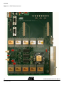
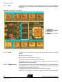
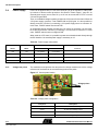
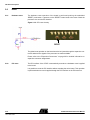
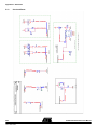
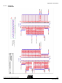
AT697 Evaluation Board .............................................................................................. User Manual Section 1 Overview............................................................................................... 1-2 1.1 Features ....................................................................................................1-2 Section 2 Hardware Description ........................................................................... 2-4 2.1 Block Diagram...........................................................................................2-4 Section 3 Ordering Information ........................................................................... 3-32 Section 4 Appendix A - Getting Started .............................................................. 4-34 4.1 4.2 4.3 4.4 4.5 4.6 4.7 AT697 Development Kit Content.............................................................4-34 Handling ..................................................................................................4-35 System Requirements.............................................................................4-35 Installing software development package ...............................................4-35 Hardware Setup ......................................................................................4-35 CD-ROM Organization ............................................................................4-37 Run your first application.........................................................................4-38 Section 5 Appendix B - Schematics.................................................................... 5-40 5.1 Evaluation Board Schematics .................................................................5-40 Section 6 Appendix C - Expansion ..................................................................... 6-52 6.1 Connector Specification ..........................................................................6-52 Section 7 Appendix D - Decoupling .................................................................... 7-54 7.1 AT697 Evaluation Board User Guide Decoupling capacitance ..........................................................................7-54 2 7540C–AERO²06/08 Overview Section 1 Overview This document describes the AT697 Evaluation Board dedicated to ATMEL AT697 processor. The AT697 is a 32-bit SPARC® V8 processor based on LEON2 fault tolerant model. The board is designed to allow an easy evaluation of the product using demonstration software. To complement the evaluation and enable additional development capability, the AT697 evaluation board provides complete access to all the processor signals. 1.1 Features The AT697 evaluation board provides the following features: On-board power supply circuitry – for external power supply sources connection – for board powering by the PCI interface On-board reset On board memories – FLASH (40-bit capability) – SRAM (two 40-bit SRAM banks) – SDRAM (one 40-bit SDRAM bank) Status indicators – Power – Error – DSU activity On-board clock circuitry – on board oscillator for clock generation – external clock source connection RS232 hardware connector dedicated to the debug support unit (DSU) RS232 hardware connector dedicated to a standard UART PCI interface User defined push-buttons User defined LEDs Two 2x50 pin expansion connector 10-pin JTAG interface connector AT697 Evaluation Board User Guide 1-2 7540C–AERO–06/08 Overview Figure 1-1. AT697 Evaluation board 1-3 7540C–AERO–06/08 AT697 Evaluation Board User Manual Section 2 Hardware Description 2.1 Block Diagram Figure 2-1. AT697 Evaluation board block diagram AT697 Integer Unit (SPARC V8) I -Cache D-Cache Flash Memory Controller FPU SRAM JTAG connector RS232 serial link Reset Control SDRAM JTAG DSU AHB AMBATM Controller AMBA bridge Reset PCI/AMBA bridge PLL control Resonator Clock Generator Push Buttons Interrupt Controller APB Watchdog Timers PCI PCI interface PIO LEDs RS232 RS232 serial link Power supply Expansion Connectors AT697 Evaluation Board User Manual 2-4 7540C–AERO–06/08 Hardware Description 2.2 Processor 2.2.1 Processor Package On the evaluation board, the AT697 32-bit SPARC processor is embedded. The processor package is the MCGA 349 space qualified package. Figure 2-2. MCGA349 package For test and component replacement facilities, the processor is mounted on a dedicated socket. The MCGA349 socket used for the AT697processor is made by Adapters-Plus. The socket reference is: CL349SA1912F Detailed information on this socket can be found at: Adapters-Plus 15 W 8TH STREET STE B. Tracy, Ca 95376 www.adapt-plus.com The direct link to the description of the socket is: http://www.adapt-plus.com/products/ic_sockets/datasheets/ds_MCGA_lockingskt.htm Figure 2-3. CL349SA1912F socket Top View 2-5 7540C–AERO–06/08 Side View AT697 Evaluation Board User Manual Hardware Description 2.2.2 Processor Pin-out Table 1. AT697 pinout - column A to G A B C D E F G VDD18 VSS18 PIO[6] PIO[1] RAMS[1] VSS18 VDD18 PIO[0] N.C. PIO[4] RAMS[2] 1 2 3 VDD18 VDD18 VSS18 VCC33 PIO[2] N.C. RAMOE[3] 4 VSS18 VDD18 PIO[9] N.C. PIO[5] PIO[3] RAMS[4] 5 N.C. N.C. PIO[11] N.C. N.C. VSS33 RAMOE[1] 6 PIO[13] PIO[10] VCC33 Reserved CB[0] N.C. VSS33 7 CB[1] VSS33 N.C. PIO[15] VSS33 PIO[12] PIO[7] 8 CB[6] CB[4] D[2] VCC33 CB[7] CB[2] PIO[8] 9 D[3] N.C. D[1] VSS33 D[6] VCC33 CB[3] 10 D[8] D[5] VCC33 VSS33 Reserved D[10] D[4] 11 D[12] VSS33 VCC33 D[13] D[7] D[15] N.C. 12 D[17] D[18] D[11] VSS33 D[14] D[16] D[19] 13 D[21] D[23] VCC33 VCC33 VSS33 VSS33 A[1] 14 D[25] N.C. D[22] D[27] N.C. VSS33 A[3] 15 D[30] N.C. D[26] D[29] N.C. N.C. A[12] 16 VSS18 VSS18 D[28] VCC33 N.C. N.C. A[6] 17 VDD18 VDD18 VSS18 D[31] N.C. A[7] VSS33 VSS18 VDD18 VCC33 A[0] A[4] A[8] VDD18 VSS18 A[2] VSS33 A[9] 18 19 Table 2. AT697 pinout - column H to P AT697 Evaluation Board User Guide H J K L M N P 1 RAMOE[0] VSS33 READ DSUACT BEXC VCC33 SDWE 2 RAMOE[2] ROMS[1] TCK DSURX SDCLK VSS33 PCI_CLK 3 VCC33 ROMS[0] TDI DSUTX DSUBRE SDDQM[1] VSS33 4 RAMOE[4] RWE[0] TDO DSUEN SDDQM[2] N.C. SDCS[0] 5 RWE[1] WRITE VSS33 TMS N.C. SDDQM[3] SDCAS 6 RWE[3] RWE[2] IOS VSS33 VSS33 GNT A/D[24] 7 RAMS[0] N.C. TRST SDDQM[0] VSS33 VCC33 A/D[30] 8 RAMS[3] VCC33 OE BRDY VCC33 A/D[21] A/D[18] 9 CB[5] PIO[14] VSS33 SDRAS A/D[22] A/D[16] A/D[17] 10 D[9] D[0] N.C. A/D[14] VSS33 PERR IRDY 11 D[20] A[5] A[16] N.C. A/D[12] A/D[9] A/D[15] 12 D[24] A[14] A[26] VDD_PLL AGNT[3] A/D[1] A/D[8] 2-6 7540C–AERO–06/08 Hardware Description H J K L M N P 13 N.C. VCC33 A[21] N.C. N.C. VSS33 A/D[5] 14 A[10] VCC33 A[27] LOCK SKEW[1] A/D[0] AGNT[1] 15 N.C. VSS33 VCC33 A[24] Reserved BYPASS CLK 16 A[11] VSS33 A[23] RESET LFT AREQ[2] VSS33 17 A[19] A[17] VSS33 VCC33 WDOG N.C. VSS33 18 A[13] A[18] A[22] VSS33 VSS_PLL AREQ[3] N.C. 19 A[15] A[20] A[25] ERROR SKEW[0] VCC33 AREQ[1] Table 3. AT697 pinout - column R to W Notes: 2-7 7540C–AERO–06/08 R T U V W 1 REQ VSS18 VDD18 2 N.C. SDCS[1] VDD18 VSS18 3 PCI_RST A/D[31] VSS18 VDD18 VDD18 4 N.C. A/D[29] VCC33 VSS18 VSS18 5 N.C. N.C. A/D[26] N.C. A/D[28] 6 N.C. A/D[27] IDSEL VSS33 A/D[25] 7 SYSEN VSS33 VCC33 C/BE[3] A/D[23] 8 VSS33 VSS33 FRAME A/D[20] A/D[19] 9 TRDY VCC33 N.C. C/BE[2] VSS33 10 PCI_LOCK DEVSEL STOP VCC33 VCC33 11 VSS33 VCC33 VSS33 C/BE[1] SERR 12 N.C. A/D[11] PAR VSS33 A/D[13] 13 VCC33 A/D[7] A/D[10] VSS33 VSS33 14 VCC33 VSS33 C/BE[0] A/D[4] A/D[6] 15 N.C. A/D[2] VCC33 N.C. A/D[3] 16 N.C. VCC33 N.C. VDD18 VSS18 17 VCC33 AGNT[0] VSS18 VDD18 VDD18 18 N.C. AGNT[2] VDD18 VSS18 19 AREQ[0] VSS18 VDD18 1. ‘Reserved’ pins shall not be driven to any voltage 2. N.C. refers to unconnected pins AT697 Evaluation Board User Manual Hardware Description 2.3 Memories The AT697 Evaluation board implements a full set of memory representative of the processor memory controller capability. All three memory areas available are implemented, including PROM, SRAM and SDRAM memories. 2.3.1 PROM (or FLASH) Two PROM capabilities are provided on the evaluation board: 1M x 8bit of FLASH for 8-bits wide bus 512k x 40bits of FLASH for 32-bit/40-bit wide bus. The ROM default configuration at delivery time is 32-bit mode (EDAC off). The Flash memories can be programmed using the DSU interface and following the sequence presented in annex E. Depending on the memory protection activation plus the bus width configuration, the size of the PROM code segment varies. The following table summarizes the different code sizes achievable for PROM area. Table 2-1. PROM code sizes Note: ROM bus width EDAC code size 8-bit enabled 384k bytes of code (1) 8-bit disabled 512k bytes of code 32-bit disabled 2M bytes of code 40-bit (32-bit + EDAC) enabled 2M bytes of code 1. Refer to the ‘EDAC on 8-bit areas’ section from the AT697 datasheet. ATMEL AT49BV802A 512K x 16 Flash memories are used on the evaluation board. These memories are 3.3V with 70ns access time capability. Figure 2-4. 8-bit PROM location 2 1 1 - 8-bit ROM 2 - 40-bit ROM 3 - ROM bus width selector 3 AT697 Evaluation Board User Guide 2-8 7540C–AERO–06/08 Hardware Description 2.3.1.1 PROM Bus Width Selector The AT697 PROM bus width is configured at reset time according to PIO[1:0] value. Under reset the processor samples PIO[1:0] and reports its value to the memory configuration register. With the evaluation board, it is possible to configure the board to use either an 8-bit wide PROM bank or a 40-bit wide PROM bank. Figure 2-5. PROM bus width selector Two on-board switches are provided to configure the PROM bus width (“PROM8” location). SW16 is used to build the static configuration at reset time: it shall be set in the ‘40’ position when the use of the 32-bit or 40-bit PROM is expected. it shall be set in the ‘8’ position when the use of the 8-bit PROM is expected SW15 is used to route the PROM chip select: it shall be set in the ‘40’ position when the use of the 32-bit or 40-bit PROM is expected. it shall be set in the ‘8’ position when the use of the 8-bit PROM is expected 2.3.1.2 8-bit PROM The 8-bit boot PROM is based on the standalone AT49BV802A flash memory (U7). The following configuration of SW15 and SW16 applies to the 8-bit mode. Table 2-2. 8-bit PROM configuration 2.3.1.3 40-bit PROM Switch State SW15 8 SW16 8 The 40-bit boot PROM is based on three AT49BV802A Flash memories (U4, U5 and U6). These chips are directly soldered on the board. In order to use the 40-bit mode, the following configuration shall be respected: 2-9 7540C–AERO–06/08 AT697 Evaluation Board User Manual Hardware Description Table 2-3. 40-bit PROM configuration Note: 2.3.1.4 PROM Expansion Switch State SW15 40 SW16 40 All the configurations for SW5 and SW16 except those specified in section 2.3.1.2 and 2.3.1.3 are forbidden. In case applied on the board, no damage happens, only is the PROM interface not functional. The AT697 processor can control up to 256Mbytes of PROM. The evaluation board can handle up to 2M bytes of PROM code. For applications that need more PROM capacity, it is possible to extend the total PROM capacity by connecting a daughter board to the expansion connectors. All PROM control signals are provided on these expansion connectors. Please refer to the “Expansion Connectors” on page 28 for details on signal assignment. AT697 Evaluation Board User Guide 2-10 7540C–AERO–06/08 Hardware Description 2.3.2 RAM The AT697 memory controller manages two types of RAM, including SRAM and SDRAM. The two memory types are implemented on-board, providing up to 68Mbytes of data/code. Figure 2-6. RAM memories implantation 1 1’ 3 1 - SRAM Bank 0 1’ - SRAM Bank 0 checkbit 2 - SRAM Bank 1 2’ - SRAM Bank 1 checkbit 3 - SDRAM 2’ 2.3.2.1 2 SRAM The evaluation board embeds two banks of SRAM. Each bank consists in five 4Mbits SRAMs. 4 SRAMs for the data/code 1 SRAM for the checkbit (EDAC protection) This provide an access to 4M bytes of SRAM data/code. The SRAM selected for the evaluation board is ATMEL’s space qualified AT6014F SRAM with 15ns access time capability. 2.3.2.2 SRAM Expansion The evaluation board is limited to 4M bytes of SRAM data/code. For application needing more SRAM capacity, it is possible to extend the total SRAM capacity by connecting a daughter board to the expansion connectors. All SRAM control signals are provided on these expansion connectors. Please refer to the “Expansion Connectors” on page 28 for details on signal assignment. 2-11 7540C–AERO–06/08 AT697 Evaluation Board User Manual Hardware Description 2.3.2.3 SDRAM The evaluation board implements one bank of SDRAM. The SDRAM size implemented is 64M bytes. The SDRAM bank is composed of three 16M x 16 SDRAMs: 2 SDRAMs for the data/code 1 SDRAM for the checkbit (EDAC protection) Micron MT48LC16M16 SDRAM are used for this board. 2.3.2.4 SDRAM expansion The evaluation board is limited to 64M bytes of SDRAM code/data. For applications that need more SDRAM capacity, it is possible to extend the total SDRAM capacity by connecting a daughter board to the expansion connectors. All SDRAM control signals are provided on these expansion connectors. Please refer to the “Expansion Connectors” on page 28 for details on signal assignment. AT697 Evaluation Board User Guide 2-12 7540C–AERO–06/08 Hardware Description 2.4 Power Supply Power can be applied via the 2.1mm Jack connector (J3) to the regulator in either polarity because of diode rectifier protection. See Section “Power supply”, page 42. An external power supply source from 5V up to 9V can be connected to J3 for on board 3.3V and 5V generation. Then, an embedded voltage regulator provides the 3.3V source for the board. When the 3.3V power supply operates, a red POWER ON led (D2) lights. It is also possible to directly power the 3.3V line by connecting a 3.3V power supply source to connector J2. In this case, ‘PWR33’ switch must be set ‘DIR’ An embedded voltage regulator provides the 1.8V source for the board. It is also possible to directly power the 1.8V line by connecting a 1.8V sources to connector J1. In this case, ‘PWR18’ switch must be configured ‘DIR’ When used as a PCI board, it is possible to power the evaluation board directly through the PCI interface. No external power supply is necessary on J3. Table 2-4. Power supply configuration power configuration 2.4.1 PWR33 PWR18 3.3V 1.8V DIR DIR not regulated not regulated REG DIR regulated not regulated DIR REG not regulated regulated REG REG regulated regulated Voltage test points comments board powering by the PCI interface available The evaluation board provides four test points for voltage measurement. All the voltage references of the board can be accessed though these test points. Figure 2-7. Current probe location Voltage probes Table 2-5. Voltage probe configuration 2-13 7540C–AERO–06/08 ‘Test point’ Description GND Ground - reference voltage VCC5 J3 main input voltage control VCC 3.3V voltage test point VDD 1.8V voltage test point AT697 Evaluation Board User Manual Hardware Description 2.4.2 Current probe The AT697 evaluation board is built to enable measurement of the processor current consumptions. Three ‘solder pads’ (I33 probe, Ipll probe & I18 probe) are provided to measure the processor currents. Figure 2-8. Current probe location current probes The following table summarizes the current consumption measurement capability. Table 2-6. Current probe configuration ‘Solder Pad’ Description Ipll probe Pll current measurement I18 probe Processor core current measurement I33 probe Processor buffer current measurement Each current probe consists in a simple “solder pad” that can be easily cut before probe insertion. Then two ports are available and the measurement tool can be inserted in the power loop. The following figure presents the “solder pad”. Figure 2-9. Solder Pad Free Area O: 0.75 mm 0.75 mm Cut Connection 2.4.3 Decoupling Capacitance The Evaluation board is designed to enable the use of the AT697 processor core at frequencies from 0Hz up to 100MHz. The PCI interface by itself can run at frequencies up to 33MHz. The following assumptions are taken for capacitance calculation: Power lines are grouped by four VDD/VSS (or VCC/VSS) pairs AT697 Evaluation Board User Guide 2-14 7540C–AERO–06/08 Hardware Description Characteristic frequencies are 33MHz and 100MHz Capacitance used have an intrinsic inductance value close 1.5nH The decoupling capacitance chosen for the evaluation board are 33nF for 33MHz decoupling 3nF for 100MHz decoupling Please refer to annex D for details on the decoupling capacitance calculation. 2-15 7540C–AERO–06/08 AT697 Evaluation Board User Manual Hardware Description 2.5 Clock The AT697 evaluation board implements two clock sources: The main processor clock (CLK) connected to a 25MHz resonator (Y3) The PCI clock (PCICLK) connected to a 33MHz resonator (Y2) Figure 2-10. Clock implantation overview Alternate Master Clock PLL Bypass Master Clock Alternate PCI Clock PCI Clock 2.5.1 AT697 Master clock The AT697 processor main clock is based on an on-board 25Mhz resonator together with the AT697 embedded PLL. This allow a processor clock generation of low and high frequency, this depending only on the PLL activation status. The PLL is activated or de-activated using the ‘BYPASS’ switch embedded. Table 2-7. PLL configuration ‘BYPASS’ Description ON The master clock frequency is equal to external frequency OFF The master clock frequency is equal to four times the external frequency The embedded resonator fits in a DIL8 socket. This makes possible the exchange of the on-board clock frequency without additional hardware. In addition, an external clock input is provided (J4) to enable injection of any clock frequency in the range of the product. The following table summarizes all the configurations available for master clock generation. Table 2-8. Master clock configuration SP4 Y3 BYPASS Comments Opened F OFF Master clock frequency is four time F Opened F ON Master clock frequency is F F OFF Master clock frequency is four time F Closed J4 Opened AT697 Evaluation Board User Guide 2-16 7540C–AERO–06/08 Hardware Description Table 2-8. Master clock configuration (Continued) SP4 J4 Y3 BYPASS Comments Closed Opened F ON Master clock frequency is F Closed F Removed OFF Master clock frequency is four time F Closed F Removed ON Master clock frequency is F Figure 2-11. Pll configuration Components for the PLL filter are fitted by default on the board. They are calculated to provide an optimized 100MHz master clock frequency. Figure 2-12. Main clock circuitry 2-17 7540C–AERO–06/08 AT697 Evaluation Board User Manual Hardware Description 2.5.2 PCI clock The PCI clock is based on a 33MHz resonator that fits in a DIL 18 socket. This makes possible the exchange of the on-board clock frequency without additional hardware. In addition, an external clock input is provided (J6) to enable injection of any clock frequency in the range of the product. Figure 2-13. PCI clock circuitry AT697 Evaluation Board User Guide 2-18 7540C–AERO–06/08 Hardware Description 2.6 Reset 2.6.1 Hardware reset The hardware reset operation of the board is performed pushing the embedded ‘RESET’ push button. A pressure on the ‘RESET’ button leads to the reset of both the processor core and the PCI interface. Figure 2-14. CPU reset circuitry RESET The global reset operation on the board can also be injected through the expansion connectors where all the signals of the processor are made available. Please refer to the “Expansion Connectors” on page 28 for detailed information on expansion connector assignments. 2.6.2 PCI reset The PCI interface of the AT697 is automatically reset when a hardware reset is applied to the board. It is possible to reset the PCI interface without resetting the entire board. This operation is performed when a reset is applied through the PCI interface on the PCI reset line. 2-19 7540C–AERO–06/08 AT697 Evaluation Board User Manual Hardware Description 2.7 Serial Link The AT697 evaluation board includes all the required hardware to manage a RS232 communication. Figure 2-15. RS232 On-board circuitry An 9-way D-type connector is provided for serial connection. The connector is a female DB9 connector. Flow control facilities are connected. Uart 1 of the AT697 is connected to this interface. The second serial link provided by the AT697 can be accessed through the expansion connector. No transceiver is implemented on board to adapt the signal levels of this second uart. Figure 2-16. Serial link placement 1 - Serial communication link 1 AT697 Evaluation Board User Guide 2-20 7540C–AERO–06/08 Hardware Description 2.8 PCI Interface The AT697 evaluation board implements a PCI interface capable to manage host and satellite configuration. The PCI interface has been designed to be integrated in compact PCI back plane. Universal keying is implemented. The board form factor fits with the 6U standard. The HOST/SATELLITE mode is configured through the HOST switch. The following configuration are applicable. Table 2-9. PCI configuration ‘HOST’ Description ON PCI interface is configured in host mode OFF PCI interface is configured in satellite mode Figure 2-17. Host/Satellite configuration 1 2-21 7540C–AERO–06/08 1 - PCI Host / Satellite configuration AT697 Evaluation Board User Manual Hardware Description 2.9 Leds The evaluation board includes 8 general purpose leds connected to the PIO interface. Figure 2-18. Leds location The following table summarizes the PIO assignment for the LEDs. Table 2-10. LEDs/PIOs assignment AT697 Evaluation Board User Guide ‘LED’ PIO assigned D5 PIO4 D6 PIO5 D7 PIO6 D8 PIO7 D9 PIO8 D10 PIO9 D11 PIO10 D12 PIO11 2-22 7540C–AERO–06/08 Hardware Description 2.10 PIOs The evaluation board includes a connector (J7) for the general purpose I/Os. All the 16 PIOs of the product are routed to this connector. Figure 2-19. PIO connector (J7) location The following table summarizes the PIO assignment on J7. Table 2-11. PIOs assignment 2-23 7540C–AERO–06/08 ‘J7’ pin number PIO assigned 1 VSS 2 PIO0 3 PIO1 4 PIO2 5 PIO3 6 PIO4 7 PIO5 8 PIO6 9 PIO7 10 PIO8 11 PIO9 12 PIO10 13 PIO11 14 PIO12 15 PIO13 16 PIO14 17 PIO15 18 VCC (3.3V) AT697 Evaluation Board User Manual Hardware Description 2.11 Pushbuttons Two user defined push-buttons are implemented on-board. These push-buttons are primarily integrated for generation of interrupts through the general purpose interface. Figure 2-20. Pushbuttons location The following table summarizes the PIO assignment for the pushbuttons. Table 2-12. Pushbuttons/PIOs ‘Pushbuttons’ PIO assigned IT1 PIO2 IT0 PIO3 IT1 pushbutton can be used to generate interrupt triggered on either rising edge or high level. IT0 pushbutton can be used to generate interrupt triggered on either falling edge or low level. Figure 2-21. Pushbuttons circuitry AT697 Evaluation Board User Guide 2-24 7540C–AERO–06/08 Hardware Description 2.12 Debug Support Unit The AT697 Debug Support Unit is based on a RS232 serial link connected to a host platform. The AT697 evaluation board includes all the required hardware to manage the RS232 communication and the debug facilities. Figure 2-22. DSU On-board circuitry A 9-way D-type connector is provided for serial connection. The connector is a female DB9 connector. This serial port is dedicated to the debug host connection. Figure 2-23. DSU interface location 1 1 - Serial communication link 3 2 - DSU Break push button 3- DSU activity indicator 2 2-25 7540C–AERO–06/08 AT697 Evaluation Board User Manual Hardware Description 2.13 JTAG Interface A 10-pin HE10 connector (J5) is provided on board to enable connection of the JTAG interface. Figure 2-24. JTAG connector 1 - JTAG connector The following table presents the assignment of the signals on the JTAG connector. Table 2-13. JTAG connector AT697 Evaluation Board User Guide J5 - JTAG connector signal name pin 1 not connected pin 2 not connected pin 3 RESET pin 4 TMS pin 5 TDI pin 6 TCK pin 7 TDO pin 8 TRST pin 9 VCC33 pin 10 GND 2-26 7540C–AERO–06/08 Hardware Description 2.14 Test Points Here is the list of the test points provided on the evaluation board. Table 2-14. Test point list PCB name Comments VCC Test point for VCC33 power supply VCC5 Test point for VCC5 power supply VDD Test point for VDD18 power supply GND Test point for ground CPU CLOCK Test point for processor main clock Figure 2-25. Power supply test points location power supply test points Figure 2-26. Main clock test point main clock test point 2-27 7540C–AERO–06/08 AT697 Evaluation Board User Manual Hardware Description 2.15 Expansion Connectors Two 2 x 50 expansion connectors are provided on the evaluation board. They are dedicated to users who want to extend the evaluation board capabilities. Table 2-15. expansion connector - J8 pin signal pin signal pin signal pin signal 1 VSS33 26 SDCLK 51 D24 76 RWE3* 2 VCC33 27 D12 52 BRDY* 77 A10 3 D0 28 SDDQM3 53 D25 78 RWE2* 4 PIO7 29 D13 54 BEXC* 79 A9 5 D1 30 SDDQM2 55 D26 80 RWE1* 6 PIO6 31 D14 56 RAMS4* 81 A8 7 D2 32 SDDQM1 57 D27 82 RWE0* 8 PIO5 33 D15 58 RAMS3* 83 A7 9 D3 34 SDDQM0 59 D28 84 CB7 10 PIO4 35 D16 60 RAMS2* 85 A6 11 D4 36 SDCS1* 61 D29 86 CB6 12 PIO3 37 D17 62 RAMS1* 87 A5 13 D5 38 SDCS0* 63 D30 88 CB5 14 PIO2 39 D18 64 RAMS0* 89 A4 15 D6 40 ROMS0* 65 D31 90 CB4 16 PIO1 41 D19 66 RAMOE4* 91 A3 17 D7 42 ROMS1* 67 RESET* 92 CB3 18 PIO0 43 D20 68 RAMOE3* 93 A2 19 D8 44 IOS* 69 CLK 94 CB2 20 SDRAS* 45 D21 70 RAMOE2* 95 A1 21 D9 46 READ 71 A13 96 CB1 22 SDCAS* 47 D22 72 RAMOE1* 97 A0 23 D10 48 WRITE* 73 A12 98 CB0 24 SDWE* 49 D23 74 RAMOE0* 99 VCC33 25 D11 50 OE* 75 A11 100 VSS33 AT697 Evaluation Board User Guide 2-28 7540C–AERO–06/08 Hardware Description Table 2-16. Expansion connector - J9 pin signal pin signal pin signal pin signal 1 VSS33 26 PLL_LOCK 51 AD24 76 C/BE0 2 VCC33 27 AD12 52 LOCK* 77 A24 3 AD0 28 BYPASS 53 AD25 78 C/BE1 4 PIO15 29 AD13 54 PERR* 79 A23 5 AD1 30 DSUEN 55 AD26 80 C/BE2 6 PIO14 31 AD14 56 GNT* 81 A22 7 AD2 32 DSUTX 57 AD27 82 C/BE3 8 PIO13 33 AD15 58 REQ* 83 A21 9 AD3 34 DSURX 59 AD28 84 AREQ3* 10 PIO12 35 AD16 60 SERR* 85 A20 11 AD4 36 DSUACT 61 AD29 86 AREQ2* 12 PIO11 37 AD17 62 TRDY* 87 A19 13 AD5 38 DSUBRE 63 AD30 88 AREQ1* 14 PIO10 39 AD18 64 IRDY 89 A18 15 AD6 40 n.c 65 AD31 90 AREQ0* 16 PIO9 41 AD19 66 STOP 91 A17 17 AD7 42 n.c 67 ERROR 92 AGNT3* 18 PIO8 43 AD20 68 IDSEL* 93 A16 19 AD8 44 n.c 69 WDOG 94 AGNT2* 20 SKWE1 45 AD21 70 DEVSEL* 95 A15 21 AD9 46 PCI_HOST 71 A27 96 AGNT1* 22 SKWE0 47 AD22 72 PCI_RST 97 A14 23 AD10 48 FRAME* 73 A26 98 AGNT0* 24 CLKDIV4 49 AD23 74 PCI_CLK 99 VCC33 25 AD11 50 PAR 75 A25 100 VSS33 See appendix B “Expansion connector” for details on the hardware placement specification of the expansion connectors. 2-29 7540C–AERO–06/08 AT697 Evaluation Board User Manual Hardware Description 2.16 Board History 2.16.1 AT697 Board Change Log This section consists in the AT697 board change log history and in the AT697 board error reporting. 2.16.1.1 AT697 Evaluation Board rev 1.1.0 First commercial version of AT697 Evaluation Board. 2.16.1.2 AT697 Evaluation Board rev 2.0.0 BYPASS switch silk-screen corrected SRAM write enable lines - RWE[3:0]* - re-assigned to the correct data byte lanes – RWE0* is connected to D[31:24] – RWE1* is connected to D[23:16] – RWE2* is connected to D[15:8] – RWE3* is connected to D[7:0] 4.7K pull-up resistors inserted on PROM chip select lines for 8-bits and 40-bits modes 2.16.2 AT697 Board Errata 2.16.2.1 Rev 1.1.0 The following sections summarize the known errors for each version of the board. BYPASS Switch silk-screen The silk-screen for the BYPASS switch is inverted. In that way, you shall set the BYPASS switch in the OFF position to disable the PLL and set the BYPASS switch in the ON position to enable the PLL SRAM RWE[3:0]* false assignement RWE0* is connected to D[7:0] whereas it should be connected to D[31:24] RWE1* is connected to D[15:8] whereas it should be connected to D[23:16] RWE2* is connected to D[23:16] whereas it should be connected to D[15:8] RWE3* is connected to D[31:24] whereas it should be connected to D[7:0] workaround : You shall enable the read-modify-write mode on the memory configuration register. PROM 8-bit mode Not operational on this revision PROM chip select pull-up request 4.7K pull -up resistor is missing on the ‘ROMS0_b_40bit’ line 4.7K pull -up resistor is missing on the ‘ROMS0_b_8bit’ line workaround : AT697 Evaluation Board User Guide 2-30 7540C–AERO–06/08 Hardware Description Insert the two pull-up resistors as presented on the following figure. 2.16.2.2 Rev 1.1.0 PROM 8-bit mode Not operational on this revision 2-31 7540C–AERO–06/08 AT697 Evaluation Board User Manual Section 3 Ordering Information ATMEL provides two AT697 Development/Evaluation environments that only differs one from each other by the tool offering. Table 3-1. Possible Order Entries AT697 Evaluation Board User Manual Part Number Processor GRMON Temperature Range Quality Flow AT697-EVAB AT697E-2E-E No 25°C Engineering AT697-DKIT AT697E-2E-E Yes 25°C Engineering 3-32 7540C–AERO–06/08 Section 4 Appendix A - Getting Started The purpose of this section is to present how to start with the AT697 Evaluation board. It describes the AT697 development environment and the simple application examples. 4.1 AT697 Development Kit Content The AT697 development environment exists in two configurations: AT697 Evaluation Board - AT697-EVAB AT697 Development Kit - AT697-DKIT The following section describes the content of the AT697 development environment. Development kit and Evaluation board only differs in their tool offering. There is neither hardware difference nor functional difference between the two versions. The only difference is the Professional Version of GRmon which is distributed in the Development Kit while no professional debug tool is provided with the Evaluation board. Hardware – AT697 Evaluation Board – AT697E Processor – One Power supply cable with 2.1mm Jack connector – Two RS232 cables Software – Gaisler Research RCC/BCC software packages – GRMON1 Professional version (under Gaisler Research License) Notes: 1. only for Development kit. Documentation – AT697 Evaluation Board User Manual – AT697 datasheet and erratasheet – BCC, RCC, and GRmon user manuals Application Samples AT697 Evaluation Board User Manual 4-34 7540C–AERO–06/08 Appendix A - Getting Started 4.2 Handling This board contains sensitive electronic components which can be damaged by Electrostatic Discharges (ESD). When handling or installing the board observe appropriate precautions and ESD safe practices. OBSERVE PRECAUTIONS FOR HANDLING ELECTROSTATIC SENSITIVE DEVICES When not in use, store the board in an electrostatic protective container or bag. 4.3 System Requirements The development software provided with the AT697 board/development kit are especially designed to run on Windows® and Linux® platforms. To run on Windows platforms, the Cygwin™ Unix emulation layer needs to be installed. Cygwin-1.1.7 (or higher) is recommended on this platform. Under Linux platform, Linux-2.4.x with glibc-2.3 (or higher) is recommended. The minimum hardware requirements are: Pentium® 1 Processor 128 MB RAM 100 MB Available Hard Disk Space 115200 Baud RS-232 Port (COM port) 4.4 Installing software development package Here is a summary of the tools provided with the AT697 evaluation board/development kit: RCC - Development suite BCC - Development suite GRMON - Debug monitor (only included in development kit) Installation procedure for each tool is specified in the corresponding User Guide. Please refer to the documents available in the “tools” section of the CD-ROM for detailed information. 4.5 Hardware Setup 4-35 7540C–AERO–06/08 In order to quickly start working with the AT697, the board is designed to allow application development and test with minimum hardware implication, except the board itself. Only a power supply source and a debug communication link are necessary to get a ready-to-work environment. AT697 Evaluation Board User Manual Appendix A - Getting Started 4.5.1 Default configuration Some switches and pads are available on the board to allow application configuration. The default configuration of the board is summarized in the following table. Table 4-1. AT697 board default configuration Switch Name Configuration Comments PWR33 REG 3.3V regulated PWR18 REG 1.8V regulated SKEW 0 no skew ARB OFF HOST OFF PCI satellite board PROM8 40 40-bit boot PROM BYPASS SP4 Note: 4.5.2 Power supply setup (1) ON OPEN 1. please refer to “Errata” section of this manual for BYPASS activation state With the default configuration, the AT697 board shall be powered from the 2.1mm Jack connector with a 5V up to 9V power supply source. A power supply source capable to deliver up to 1A shall be used (1A figure can be achieved when daughter boards are connected to the expansion connectors). It is strongly recommended that the power supply is current limited in order to prevent damage to the board or power supply in case of over-current. On-board voltage regulators generate the regulated +3.3V power supply for the processor, the memories and the peripheral devices, and the +1.8V power supply for the processor. If used in a PCI (Compact PCI) backplane providing power supply, it is strictly forbidden to connect a power supply to the AT697 evaluation board. In this case the power supply is guaranteed by the power supply contacts on the PCI connector. Figure 4-1. Power Supply connection 4.5.3 Serial Communication link For application download and debug, you shall connect the serial interface of the board to the host monitor. With the AT697 Development kit, the GRmon debug monitor from Gaisler Research is available. AT697 Evaluation Board User Guide 4-36 7540C–AERO–06/08 Appendix A - Getting Started 4.5.3.1 GRMON GRMON requires a single RS232 communication link to enable load and debug of applications. Just connect the RS232 cable to the board DSU connector (P1) and to one of the host platform RS232 connector. The host platform running GRMON under Linux or Windows environment is then used to establish the communication with the AT697 processor. Figure 4-2. Host Connection 4.6 CD-ROM Organization The CD-ROM provided with the evaluation board has the following architecture: /documents - It contains all the documentation related to AT697 processor and AT697 Evaluation board. /documents/at697 /documents/at697/AT697E_errata.pdf /documents/at697/AT697_datasheet.pdf /documents/at697_evab /documents/at697_evab/AT60142F_FT_datasheet.pdf /documents/at697_evab/AT697_EVAB_2_0.0_schematics.pdf /documents/at697_evab/AT697_EVAB_user_guide.pdf /tools - It contains all the tool packages necessary to build a full development environment based on the AT697 Evaluation board /tools/debugger /tools/debugger/grmon-pro-1.1.19.tar.tar /tools/debugger/grmon.pdf /tools/debugger/hasp /tools/debugger/hasp/ini_files /tools/debugger/hasp/ini_files/IPX_Broadcast.zip /tools/debugger/hasp/ini_files/IPX_No_Sap.zip /tools/debugger/hasp/ini_files/Standard_Nethasp.zip /tools/debugger/hasp/ini_files/tcpip.zip /tools/debugger/hasp/install.pdf /tools/debugger/hasp/linux 4-37 7540C–AERO–06/08 AT697 Evaluation Board User Manual Appendix A - Getting Started /tools/debugger/hasp/linux/driver /tools/debugger/hasp/linux/driver/HDD_Linux_dinst.tar.gz /tools/debugger/hasp/linux/driver/aksusbd-redhat-1.8.1-2.i386.rpm /tools/debugger/hasp/linux/driver/aksusbd-suse-1.8.1-2.i386.rpm /tools/debugger/hasp/linux/driver/readme.txt /tools/debugger/hasp/linux/server /tools/debugger/hasp/linux/server/hasplm /tools/debugger/hasp/linux/server/hasplm-redhat-8.30-1.i386.rpm /tools/debugger/hasp/linux/server/hasplm-suse-8.30-1.i386.rpm /tools/debugger/hasp/linux/server/readme.txt /tools/debugger/hasp/macosx /tools/debugger/hasp/macosx/driver /tools/debugger/hasp/macosx/driver/HDD_Installer_MacOSX.dmg /tools/debugger/hasp/macosx/driver/HDD_Installer_MacOSX_Tiger_only.zip /tools/debugger/hasp/macosx/server /tools/debugger/hasp/macosx/server/LM_Setup_Mac.dmg /tools/debugger/hasp/windows /tools/debugger/hasp/windows/driver /tools/debugger/hasp/windows/driver/HASPUserSetup.exe /tools/debugger/hasp/windows/driver/readme.txt /tools/debugger/hasp/windows/server /tools/debugger/hasp/windows/server/lmsetup.exe /tools/debugger/hasp/windows/server/readme.txt /tools/development_platform /tools/development_platform/bcc /tools/development_platform/bcc/sparc-elf-3.2.3-1.0.22-cygwin.tar.gz /tools/development_platform/bcc/win32-sparc-elf-3.2.3-1.0.22.exe /misc - It contains some additional user files from AT697 environment such as BSDL file and IBIS model of the AT697. /misc /misc/bsdl /misc/bsdl/AT697.bsd.gz /misc/ibis_model /misc/ibis_model/at697.ibs /misc/schematics_brd /misc/schematics_brd/AT697_board.brd /src - It contains some simple code samples that can be directly run on AT697 target. Source code as well as executables are provided. The src folder is built as follow : – /demo : it contains the main files, makefiles and executable for all demonstrations – /lib : it contains some services libraries that can be used for application development – /lib_at697 : it contains the low level drivers used that fits AT697 processor ressources AT697 Evaluation Board User Guide 4-38 7540C–AERO–06/08 Appendix A - Getting Started /src/common /src/common/demo /src/common/demo/Paranoia /src/common/demo/Paranoia/hex /src/common/demo/Paranoia/hex/paranoia /src/common/demo/Paranoia/makefile /src/common/demo/Paranoia/obj /src/common/demo/Paranoia/obj/paranoia.o /src/common/demo/Paranoia/paranoia.c /src/common/demo/blink /src/common/demo/blink/Makefile /src/common/demo/blink/dump.s /src/common/demo/blink/hex /src/common/demo/blink/hex/ram_blink /src/common/demo/blink/hex/ram_blink.txt /src/common/demo/blink/hex/rom_blink /src/common/demo/blink/hex/rom_blink.txt /src/common/demo/blink/main1.c /src/common/demo/blink/obj /src/common/demo/blink/obj/main.o /src/common/demo/dhrystone /src/common/demo/dhrystone/Makefile /src/common/demo/dhrystone/dhry.h /src/common/demo/dhrystone/dhry_1.c /src/common/demo/dhrystone/dhry_2.c /src/common/demo/dhrystone/hex /src/common/demo/dhrystone/hex/dhry /src/common/demo/dhrystone/obj /src/common/demo/dhrystone/obj/dhry1.o /src/common/demo/dhrystone/obj/dhry2.o /src/common/demo/flash32 /src/common/demo/flash32/Makefile /src/common/demo/flash32/hex /src/common/demo/flash32/hex/flash32 /src/common/demo/flash32/hex/flash32.txt /src/common/demo/flash32/main.c /src/common/demo/flash32/obj /src/common/demo/flash32/obj/main.o /src/common/demo/flash8 /src/common/demo/flash8/Makefile /src/common/demo/flash8/hex /src/common/demo/flash8/hex/flash8 /src/common/demo/flash8/hex/flash8.txt /src/common/demo/flash8/main.c /src/common/demo/flash8/obj /src/common/demo/flash8/obj/main.o /src/common/demo/hello_world /src/common/demo/hello_world/Makefile /src/common/demo/hello_world/hex /src/common/demo/hello_world/hex/ram_hello /src/common/demo/hello_world/hex/ram_hello.txt /src/common/demo/hello_world/main1.c /src/common/demo/hello_world/obj /src/common/demo/uart_splash /src/common/demo/uart_splash/Makefile /src/common/demo/uart_splash/config.h /src/common/demo/uart_splash/dump.s /src/common/demo/uart_splash/hex /src/common/demo/uart_splash/hex/demo_uart /src/common/demo/uart_splash/hex/rom_demo_uart /src/common/demo/uart_splash/obj /src/common/demo/uart_splash/obj/uart_lib.o /src/common/demo/uart_splash/obj/uart_main.o /src/common/demo/uart_splash/uart_main.c /src/common/drv_at697 /src/common/drv_at697/uart /src/common/drv_at697/uart/uart_drv.h /src/common/lib /src/common/lib/uart /src/common/lib/uart/uart_lib.c /src/common/lib/uart/uart_lib.h 4-39 7540C–AERO–06/08 AT697 Evaluation Board User Manual Appendix A - Getting Started 4.7 Run your first application Once GRmon and BCC/RCC are installed on your platform and your hardware in the default configuration, you are ready to start development session on the AT697 target. 4.7.1 Compiling and Linking your program The BCC/RCC development environment provide a full tool set for compiling and linking your application. You can compile and link your basic application with the following command : sparc-elf-gcc -g -O2 application.c -o application Here is a capture of the compile/link step. In addition, you can create the ROM boot strap using sparc-elf-mkprom application -o rom_application Figure 4-3. Compile/Link with RCC & ROM boot strap building (Cygwin environment) 4.7.2 Transfering the executable file to board Open a terminal window on your host platform in order to run GRmon (refer to GRmon user manual for details). When the board is configured with the PLL bypass switch in the ‘ON’ position, the processor clock frequency is 25MHz (default). In this case, use the following command to start a GRmon session: under WINDOWS: "grmon -leon2 -uart COM1 -baud 115200" under LINUX: "grmon -leon2 -uart /dev/ttyS0 -baud 115200” where the "-uart" and "-baud" flags are to be set according to your communication interface configuration. When the board is configured with the PLL bypass switch in the ‘OFF’ position, the processor clock frequency is 100MHz. In this case, use the following command to start a GRmon session: under WINDOWS: "grmon -leon2 -uart COM1 -baud 115200 -romws 15 -ramws 3" under LINUX: "grmon -leon2 -uart /dev/ttyS0 -baud 115200 -romws 15 -ramws 3" where the "-uart" and "-baud" flags are to be set according to your communication interface configuration, and the “-romws” and “-ramws” flags are to be tuned with respect to the AT697E internal clock frequency. Other options can be added to the command line. Please refer to the GRmon user manual for more details. Once connected to the target, you can load the application to the on-board memory. AT697 Evaluation Board User Guide 4-40 7540C–AERO–06/08 Appendix A - Getting Started 4.7.2.1 Load to ROM The ROM boot strap can be loaded to the on board flash applying the following commands : flash enable flash erase all flash load rom_application 4.7.2.2 Load to RAM The executable can also be loaded to RAM applying the following commands : load application 4.7.3 Running the application The application can then be directly run on the target using the run command : run Figure 4-4. “Hello World” load & execution (Native Windows environment) 4-41 7540C–AERO–06/08 AT697 Evaluation Board User Manual Appendix A - Getting Started 4.7.4 Demonstration Before building your own application, you can start the Evaluation board with the demonstration software provided on the CDROM. Just load one of the applications from src/common/demo/demoname/hex/application path directly to RAM and launch the run command through GRmon. AT697 Evaluation Board User Guide 4-42 7540C–AERO–06/08 Section 5 Appendix B - Schematics 5.1 Evaluation Board Schematics Here is the list of the schematics of the AT697 evaluation board: AT697 processor Power supply Clock and Reset ROM memory interface SRAM memory interface SDRAM memory interface Serial communication links PCI interface User interface Expansion connectors Note: AT697 Evaluation Board User Manual Due to the size of the original schematic, size reduction have been performed for integration in this document. A more precise view on the schematics can be provided under request. For more information, please contact ATMEL hotline at [email protected]. 5-40 7540C–AERO–06/08 Appendix B - Schematics 5.1.1 AT697 processor 5-41 7540C–AERO–06/08 AT697 Evaluation Board User Manual Appendix B - Schematics 5.1.2 Power supply AT697 Evaluation Board User Guide 5-42 7540C–AERO–06/08 Appendix B - Schematics 5.1.3 Clock and Reset 5-43 7540C–AERO–06/08 AT697 Evaluation Board User Manual Appendix B - Schematics 5.1.4 ROM memory AT697 Evaluation Board User Guide 5-44 7540C–AERO–06/08 Appendix B - Schematics 5.1.5 SRAM memory 5-45 7540C–AERO–06/08 AT697 Evaluation Board User Manual Appendix B - Schematics 5.1.6 SDRAM memory AT697 Evaluation Board User Guide 5-46 7540C–AERO–06/08 Appendix B - Schematics 5.1.7 Serial Links 5-47 7540C–AERO–06/08 AT697 Evaluation Board User Manual Appendix B - Schematics 5.1.8 PCI AT697 Evaluation Board User Guide 5-48 7540C–AERO–06/08 Appendix B - Schematics 5.1.9 User Interface 5-49 7540C–AERO–06/08 AT697 Evaluation Board User Manual Appendix B - Schematics 5.1.10 Expansion connectors AT697 Evaluation Board User Guide 5-50 7540C–AERO–06/08 Section 6 Appendix C - Expansion In order to interface the AT697 evaluation board with an expansion board, two specific connectors are used. These are two 2x50 headers soldered at the top side of the Board. They are male 2x50 CMS high density connectors. Figure 6-1. Board to board Connection with the Expansion Connectors Expansion Board TOP BOTTOM Expansion Board Connectors - Female Part AT697 Evaluation Board Connectors - Male Part TOP AT697 Evaluation Board BOTTOM The two expansion connectors provide a full access to all the signals of the AT697 processor. The pin assignment of these two connectors is available in Section “Expansion Connectors”, page 28 of this document. 6.1 Connector Specification The expansion interface is based on two high density connectors. The implementation chosen for the AT697 evaluation board relies on two 2x50 male Bergstak® connectors. Here is the reference of the connector embedded on the evaluation board: Male 2x50 Bergstak CMS provided by Farnell under 973-324 reference The connection of a mezzanine board to the evaluation board can be performed using the following reference: Female 2x50 Bergstak CMS provided by Farnell under 973-336 reference AT697 Evaluation Board User Manual 6-52 7540C–AERO–06/08 Appendix C - Expansion 6.2 Mechanical Constraints The following figure presents the mechanical constraints for development of an expansion board that can be plugged on the AT697 evaluation board. All dimensions are given at more or less 0.20mm. Figure 6-2. Mechanical constraints. Note: 6-53 7540C–AERO–06/08 If more information is required, an AT697.brd file is available under request. This document can be sent to any customer requiring a global view of the board and requiring additional measurement constraints over the board. Such file can be read and analyzed with “Allegro Free Physical Viewer”, a free tool from Cadence®. AT697 Evaluation Board User Manual Section 7 Appendix D - Decoupling 7.1 Decoupling capacitance Two main frequencies are involved in the AT697 processor environment: 33MHz from the PCI interface 100MHz from the master clock of the processor (either from PLL or directly from resonator input) The hypothesis used as a first evaluation of the decoupling capacitance are the following: Capacitor description 1.5nH 0.75nH capacitor 0.75nH PCB – 1.5nH from the connection of the capacitor to the PCB – 1.5nH from the capacitor intrinsic inductance This hypothesis corresponds to a capacitor connected to two micro-vias on a PCB. According to the two main frequencies from the product, the decoupling capacitances where chosen considering that the frequencies to filter are 100MHz and 33MHz The frequencies to cut are defined by: 1 fc = ------------------· 2 π L· C with – L: the inductance equivalent to the global inductance on the VSS/VDD line. – C: the decoupling capacitance. AT697 Evaluation Board User Manual 7-54 7540C–AERO–06/08 Appendix D - Decoupling Then, the decoupling capacitance chosen for the evaluation board are 10nF for 33MHz decoupling 1nF for 100MHz decoupling A more precise model to calculate the decoupling capacitors will be inserted in the first official release of this document. This model will include the model of the processor plus the model of the socket. 7-55 7540C–AERO–06/08 AT697 Evaluation Board User Manual Atmel Headquarters Atmel Operations Corporate Headquarters Memory 2325 Orchard Parkway San Jose, CA 95131 TEL 1(408) 441-0311 FAX 1(408) 487-2600 Europe Atmel Sarl Route des Arsenaux 41 Case Postale 80 CH-1705 Fribourg Switzerland TEL (41) 26-426-5555 FAX (41) 26-426-5500 Asia Room 1219 Chinachem Golden Plaza 77 Mody Road Tsimhatsui East Kowloon Hong Kong TEL (852) 2721-9778 FAX (852) 2722-1369 Japan 9F, Tonetsu Shinkawa Bldg. 1-24-8 Shinkawa Chuo-ku, Tokyo 104-0033 Japan TEL (81) 3-3523-3551 FAX (81) 3-3523-7581 2325 Orchard Parkway San Jose, CA 95131 TEL 1(408) 441-0311 FAX 1(408) 436-4314 Microcontrollers 2325 Orchard Parkway San Jose, CA 95131 TEL 1(408) 441-0311 FAX 1(408) 436-4314 La Chantrerie BP 70602 44306 Nantes Cedex 3, France TEL (33) 2-40-18-18-18 FAX (33) 2-40-18-19-60 ASIC/ASSP/Smart Cards RF/Automotive Theresienstrasse 2 Postfach 3535 74025 Heilbronn, Germany TEL (49) 71-31-67-0 FAX (49) 71-31-67-2340 1150 East Cheyenne Mtn. Blvd. Colorado Springs, CO 80906 TEL 1(719) 576-3300 FAX 1(719) 540-1759 Biometrics/Imaging/Hi-Rel MPU/ High Speed Converters/RF Datacom Avenue de Rochepleine BP 123 38521 Saint-Egreve Cedex, France TEL (33) 4-76-58-30-00 FAX (33) 4-76-58-34-80 Zone Industrielle 13106 Rousset Cedex, France TEL (33) 4-42-53-60-00 FAX (33) 4-42-53-60-01 1150 East Cheyenne Mtn. Blvd. Colorado Springs, CO 80906 TEL 1(719) 576-3300 FAX 1(719) 540-1759 Scottish Enterprise Technology Park Maxwell Building East Kilbride G75 0QR, Scotland TEL (44) 1355-803-000 FAX (44) 1355-242-743 e-mail [email protected] Web Site http://www.atmel.com Disclaimer: The information in this document is provided in connection with Atmel products. No license, express or implied, by estoppel or otherwise,to anyintellectualproperty right is granted by this document or in connection with the sale of Atmel products. EXCEPT AS SET FORTH IN ATMEL’S TERMS AND CONDI-TIONS OF SALE LOCATED ON ATMEL’S WEB SITE, ATMEL ASSUMES NO LIABILITY WHATSOEVER AND DISCLAIMS ANY EXPRESS, IMPLIED OR STATUTORYWARRANTY RELATING TO ITS PRODUCTS INCLUDING, BUT NOT LIMITED TO, THE IMPLIED WARRANTY OF MERCHANTABILITY, FITNESS FOR A PARTICULARPURPOSE, OR NON-INFRINGEMENT. IN NO EVENT SHALL ATMEL BE LIABLE FOR ANY DIRECT, INDIRECT, CONSEQUENTIAL, PUNITIVE, SPECIAL OR INCIDEN-TAL DAMAGES (INCLUDING, WITHOUT LIMITATION, DAMAGES FOR LOSS OF PROFITS, BUSINESS INTERRUPTION, OR LOSS OF INFORMATION) ARISING OUTOF THE USE OR INABILITY TO USE THIS DOCUMENT, EVEN IF ATMEL HAS BEEN ADVISED OF THE POSSIBILITY OF SUCH DAMAGES. Atmel makes norepresentationsor warranties with respect to the accuracy or completeness of the contents of this document and reserves the right to make changes to specificationsand product descriptions at any time without notice. Atmel does not make any commitment to update the information contained herein. Unless specifically provided otherwise, Atmel products are not suitable for, and shall not be used in, automotive applications. Atmel’s products are not intended, authorized, or warranted for useas components in applications intended to support or sustainlife. © Atmel Corporation 2008. All rights reserved. Atmel ®, logo and combinations thereof, and Everywhere You Are ® and others are the registered trademarks or trademarks of Atmel Corporation or its subsidiaries. Windows® and others are registered trademarks of Microsoft Corporation. Other terms and product names may be trademarks of others. Printed on recycled paper. 7540C–AERO–06/08 /xM