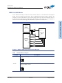
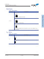
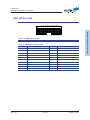
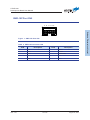
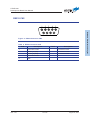
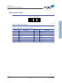
1
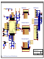
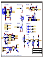
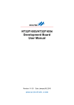
HT32F125x Development Board
User Manual
Revision: V1.01
Date: ���������������
August 22, 2011
32-bit ARM Cortex™-M3 MCU
HT32 Series
Table of Contents
1 Introduction.............................................................................................................. 5
Features................................................................................................................................. 6
2 Hardware Placement and Layout........................................................................... 7
Boot Option........................................................................................................................... 11
VBAT Option............................................................................................................................ 11
SWD-20P Port CN4.............................................................................................................. 12
SWD-10P Port CN5.............................................................................................................. 13
RS232 CN2........................................................................................................................... 14
Multi-Interface CN6............................................................................................................... 15
Extension Connector CN3 & CN7......................................................................................... 16
Mini USB Type B Connector CN1......................................................................................... 17
3 Component Jumpers............................................................................................. 18
4 Schematics............................................................................................................. 19
Rev. 1.01
2 of 22
August 22, 2011
Table of Contents
RS232 & USB Mode............................................................................................................. 10
32-bit ARM Cortex™-M3 MCU
HT32 Series
List of Figures
Rev. 1.01
1. HT32F125x Development Board............................................................................................... 5
2. HT32F125x Development Board Block Diagram....................................................................... 7
3. HT32F125x Development Board PCB layout............................................................................ 8
4. HT32F125x Development Board Peripheral Device Placement................................................ 9
5. RS232 / USB Jumper Switch Block Diagram.......................................................................... 10
6. SWD-20P Port CN4................................................................................................................. 12
7. SWD-10P Port CN5................................................................................................................. 13
8. RS232 Connector CN2............................................................................................................ 14
9. Multi-Interface CN6.................................................................................................................. 15
10. Extension Connector CN3 & CN7......................................................................................... 16
11. Mini USB type B Connector CN1........................................................................................... 17
12. MCU, Extension Connector, SWD and Multi-interface.......................................................... 20
13. USB, RS232, Switches, Potentiometer, LED, Flash, EEPROM and Buzzer......................... 21
3 of 22
August 22, 2011
List of Figures
Figure
Figure
Figure
Figure
Figure
Figure
Figure
Figure
Figure
Figure
Figure
Figure
Figure
32-bit ARM Cortex™-M3 MCU
HT32 Series
List of Tables
Rev. 1.01
1. USART Mode Jumpers............................................................................................................. 10
2. Boot Jumpers.............................................................................................................................11
3. VBAT Jumpers..............................................................................................................................11
4. SWD-20P Connector CN4........................................................................................................ 12
5. SWD-10P Connector CN5........................................................................................................ 13
6. RS232 Connector CN3............................................................................................................. 14
7. Multi-Interface Connector CN10................................................................................................ 15
8. Extension Connector CN3......................................................................................................... 16
9. Extension Connector CN7......................................................................................................... 16
10. Mini USB type B Connector CN1............................................................................................ 17
11. Component Jumpers............................................................................................................... 18
4 of 22
August 22, 2011
List of Tables
Table
Table
Table
Table
Table
Table
Table
Table
Table
Table
Table
HT32F125x
Development Board User Manual
1
Introduction
The HT32F125x development board is designed for the HT32F125x series of microcontrollers. The
HT32F125x series of microcontrollers contain a variety of peripheral functions such as high speed
SAR A/D Converter, Operational Amplifiers, I2C interface, USART interface, SPI interface, Timer
Modules, Watchdog Timer, Real Time Clock, Serial Wire Debug Interface etc..
Figure 1. HT32F125x Development Board
Rev. 1.01
5 of 22
August 22, 2011
Introduction
The development board is provided with some specific components to assist with device peripheral
function operation such as RS232 connector, USB1.1 device controller, EEPROM, potentiometer
and so on..
HT32F125x
Development Board User Manual
Features
Rev. 1.01
USB1.1 full speed connection – uses HT45B0K
5V power supply: mini USB connector
RS232 connector
Reset, wakeup and two key buttons
Three LEDs
I2C-compatible serial interface EEPROM
SPI-compatible serial interface Flash – optional
SPI and I2C extended interfaces for LCD display application - optional multi-interface
PWM output for Buzzer driving
Backup battery
Boot from Flash, SRAM or boot loader
SWD-10P, SWD-20P 10-pin and 20-pin SWD serial-wire debug port interface
6 of 22
August 22, 2011
Introduction
▀
▀
▀
▀
▀
▀
▀
▀
▀
▀
▀
▀
HT32F125x
Development Board User Manual
2
Hardware Placement and Layout
I/O Extension-20P
SPI / I2C Extension
BUZZER
RS-232
5V-to-3.3V
Transceiver
JUMPER
RS-232
JUMPER
HT32F1253
ARM Cortex-M3
Microcontroller
SWD-10P
I2C
EEPROM
SPI
FLASH
8 MHz
5V-to-3.3V
Regulator
POWER
LED
RESET
32.768 kHz
HT45B0K
SPI-to-USB
Bridge
Mini-USB
I/O Extension-20P
SWD-20P
CR1220
3V Battery
WAKE
UP
KEY1
KEY2
Figure 2. HT32F125x Development Board Block Diagram
Rev. 1.01
7 of 22
August 22, 2011
Hardware Placement and Layout
VR
HT32F125x
Development Board User Manual
Hardware Placement and Layout
Figure 3. HT32F125x Development Board PCB layout
Rev. 1.01
8 of 22
August 22, 2011
HT32F125x
Development Board User Manual
USART DB9
Connector
RS232
Transceiver
Extension
Connector
USART
SPI to USB
Bridge
(HT45B0K)
64K bit
EEPROM
GPIO
I2C
3 x LEDs
3 x Buttons
HT32F1253
MultiInterface
8M byte
Series Flash
SPI
Potentiometer
ADC
SWD-10P
Connector
SWD
SWD-20P
Connector
Figure 4. HT32F125x Development Board Peripheral Device Placement
Rev. 1.01
9 of 22
August 22, 2011
Hardware Placement and Layout
Mini USB
Connector
HT32F125x
Development Board User Manual
RS232 & USB Mode
As the RS232 and USB ports share the same USART interface on the HT32F125x development
board, only one of them can be chosen. This is implemented using the J8 & J9 jumpers. For
example, to use the USB interface, the J8 and J9 jumpers must first select the USB mode and J4~7
& J24 must also bedconnected. Additionalls, the USART to SPI mode must be configured by
software to control the USB bridge, the (HT45B0K, to implement a USB function.
Hardware Placement and Layout
SP3232
RS232
Transceiver
J8
R1 OUT
PA8/USART Rx
T1 IN
SPI OUT
HT32F1253
MCU
J9
PA9/USART Tx
SPI IN
PA1 PA2 PA3 PA7 PA4
HT45B0K
SPI to USB
Bridge
INTB
CLKI
CSCB
SCK
D+ Pull-high
J4
J5
J6
J7
J24
Figure 5. RS232 / USB Jumper Switch Block Diagram
Table 1. USART Mode Jumpers
Jumper
Description
RS232 mode setting.
J9 J8
J9 & J8
USB mode setting - here J4~J7 and J24 also need to be connected for the USB
bridge, HT45B0K, control.
J9 J8
Rev. 1.01
10 of 22
August 22, 2011
HT32F125x
Development Board User Manual
Boot Option
Table 2. Boot Jumpers
Jumper
Description
Boot loader mode
J2 J1
1
Hardware Placement and Layout
0
Boot from the embedded boot loader.
SRAM mode
J2 J1
1
J1 & J2
0
Boot from the embedded SRAM
Main flash mode
J2 J1
1
0
Boot from the embedded main flash. BOOT0 (J1) don’t care and BOOT1 (J2) = 1
(default setting)
VBAT Option
Table 3. VBAT Jumpers
Jumper
Description
VBAT pin is connected to the 3.3V power - default setting
VBAT
J3
VDD
J3
VBAT pin is connected to the 3V CR1220 battery
VBAT
J3
VDD
Rev. 1.01
11 of 22
August 22, 2011
HT32F125x
Development Board User Manual
SWD-20P Port CN4
2 4 6 8 10 12 14 16 18 20
Figure 6. SWD-20P Port CN4
Table 4. SWD-20P Connector CN4
Pin#
Rev. 1.01
Description
Pin#
Description
1
3.3V
2
3.3V
3
N.C.
4
GND
5
N.C.
6
GND
7
SWDIO
8
GND
9
SWCLK
10
GND
11
Pull-high
12
GND
13
TRACESWO
14
GND
15
Reset#
16
GND
17
N.C.
18
GND
19
N.C.
20
GND
12 of 22
August 22, 2011
Hardware Placement and Layout
1 3 5 7 9 11 13 15 17 19
HT32F125x
Development Board User Manual
SWD-10P Port CN5
2 4 6 8 10
Figure 7. SWD-10P Port CN5
Table 5. SWD-10P Connector CN5
Pin#
Rev. 1.01
Description
Pin#
Description
1
3.3V
2
SWDIO
3
GND
4
SWCLK
5
GND
6
TRACESWO
7
N.C.
8
N.C.
9
GND
10
Reset
13 of 22
August 22, 2011
Hardware Placement and Layout
1 3 5 7 9
HT32F125x
Development Board User Manual
RS232 CN2
1
2
7
5
4
8
9
Figure 8. RS232 Connector CN2
Table 6. RS232 Connector CN3
Pin#
Rev. 1.01
Description
Pin#
Description
1
Connected to PIN4
6
Connected to PIN1
2
USART_Rx (PA8)
7
Connected to PIN8
3
USART_Tx (PA9)
8
Connected to PIN7
4
Connected to PIN6
9
NC
5
GND
14 of 22
August 22, 2011
Hardware Placement and Layout
6
3
HT32F125x
Development Board User Manual
Multi-Interface CN6
2 4 6 8 10 12 14
Figure 9. Multi-Interface CN6
Table 7. Multi-Interface Connector CN10
Pin#
Rev. 1.01
Description
Pin#
Description
1
3.3V
2
GND
3
PB3
4
N.C.
5
PB5
6
PB6
7
PB15
8
PB14
9
PB13
10
PA11
11
PA12
12
PB4
13
GND
14
DC5V
15 of 22
August 22, 2011
Hardware Placement and Layout
1 3 5 7 9 11 13
HT32F125x
Development Board User Manual
Extension Connector CN3 & CN7
2 4 6 8 10 12 14 16 18 20
Figure 10. Extension Connector CN3 & CN7
Table 8. Extension Connector CN3
Pin#
Description
Pin#
Description
1
GND
2
3.3V
3
PA15
4
PA14
5
PA13
6
PA12
7
PA11
8
PB11
9
PB10
10
PB9
11
PB8
12
PA4
13
PA5
14
PA6
15
PA7
16
PA8
17
PA9
18
PA10
19
DC5V
20
GND
Table 9. Extension Connector CN7
Pin#
Rev. 1.01
Description
Pin#
Description
1
GND
2
3.3V
3
PB15
4
PB14
5
PB13
6
PB12
7
PB0
8
PB1
9
PB2
10
PB3
11
PB4
12
PB5
13
PB6
14
PB7
15
PA0
16
PA1
17
PA2
18
PA3
19
DC5V
20
GND
16 of 22
August 22, 2011
Hardware Placement and Layout
1 3 5 7 9 11 13 15 17 19
HT32F125x
Development Board User Manual
Mini USB Type B Connector CN1
1
2
3
4
5
Table 10. Mini USB type B Connector CN1
Pin#
Rev. 1.01
Description
Pin#
Description
1
USB_5V
2
D-
3
D+
4
N.C.
5
GND
17 of 22
August 22, 2011
Hardware Placement and Layout
Figure 11. Mini USB type B Connector CN1
HT32F125x
Development Board User Manual
3
Component Jumpers
The component jumpers are used to connect up the components. For example, J13 will be
connected to LED D3 to allow the LED to be switched on and off by the application program.
Table 11. Component Jumpers
Jumper#
Description
J1
PA9
Select boot0 input 0 (low) or 1 (high)
J2
PA10
Select boot1 input 0 (low) or 1 (high)
J3
VBAT
Select VBAT power source (VDD or Battery)
J4
PA1
Connected to HT45B0k INTB
J5
PA2
Connected to HT45B0k CLK
J6
PA3
Connected to HT45B0k SCSB
J7
PA7
Connected to HT45B0k SCK
J8
PA8
Switch between RS232 or USB Mode
J9
PA9
Switch between RS232 or USB Mode
J10
PB10
Connected to wakeup button
J11
PB11
Connected to key1 button
J12
PA10
Connected to key2 button
J13
PA5
Connected to LED (D3)
J14
PA6
Connected to LED (D4)
J15
PB12
Connected to LED (D5)
J16
PA11
Connected to HT24LC64 SCL
J17
PA12
Connected to HT24LC64 SDA
J18
PB7
Connected to MX25L6406E CS
J19
PB14
Connected to MX25L6406E SO
J20
PB13
Connected to MX25L6406E SCLK
J21
PB15
Connected to MX25L6406E SI
J22
PB2
Connected to buzzer
J23
PA0
Connected to potentiometer
J24
PA4
USB D+ Pull-high control
J25
VDD33
MCU 3.3V power input
18 of 22
August 22, 2011
Component Jumpers
Rev. 1.01
PIN of HT32F1253
HT32F125x
Development Board User Manual
4
Schematics
This section shows the complete circuit of the HT32F125x development board:
Rev. 1.01
19 of 22
August 22, 2011
Schematics
▀ Figure 12 includes the MCU, Extension Connector, SWD-10P Connector, SWD-20P Connector
and Multi-interface.
▀ Figure 13 includes the USB and RS232 interfaces, Switches, Potentiometer, LED, Flash,
EEPROM, and Buzzer.
C11
2.2uF
C10
0.01uF
C7
12p R7
12p
R6
0
1M
C9
0.01uF
X2
48
47
46
45
44
43
42
41
40
39
38
37
BEAD
C8
10
9
8
7
6
5
4
3
2
1
CN6
VDD
PB3/MRESET
L1
R8
0
SWJCN5Connector
Mult-Interface
DC5V
PB4/IO_D_SHDN
PA12/I2C_SDA
PA11/I2C_SCL
PB13/SPI_SCK
PB14/SPI_MISO
PB15/SPI_MOSI
PB6/IO_D_CSB
PB5/IO_PENIRQ
MVDD
MVDD
Mult-Interface
14
13
12
11
10
9
8
7
6
5
4
3
2
1
BEAD
PB0/XTALIN
L3
BEAD
PB1/XTALOUT
L2
PB7/SPI_SEL
PB6/IO_D_CSB
PB5/IO_PENIRQ
PB4/IO_D_SHDN
PB3/MRESET
PB2/TM_BZ
USBGND
CRYSTAL
RESET
R1
10K
VSSA_1
VDDA
VSS33_1
VDD33_1
PB7
PB6
PB5
PB4
PB3
PB2
VDD18
VDD18
PA9/USART_TX
MVDD
J2
1
C2 0.1uF
C3 4.7uF
MVDD
PA15/SWO
PA14/SWCLK
PA13/SWDIO
20
19
18
17
16
15
14
13
12
11
10
9
8
7
6
5
4
3
2
1
VDD
VDD
JTREST
JTDI
JTMS/SWDIO
JTCK/SWCLK
JTDO/SWO
RESET
RTCK
DBGRQ
DBGACK
GND
GND
GND
GND
GND
GND
GND
GND
GND
C30
0.1uF
DC5V
VDD
Extension Connector 1
VDD
1
2
3
5
7
9
13
15
11
17
19
4
6
8
10
12
14
16
18
20
SWD-20P
R14 100
PA13/SWDIO
0.1uF
VBAT
R3
R4
0
10M
R5
0
X1
C5
CRYSTAL
C6
10pF
DC5V
R15 100
R16 100
PA14/SWCLK
PA15/SWO
VDD
20
19
18
17
16
15
14
13
12
11
10
9
8
7
6
5
4
3
2
1
10pF
PB9/XTAL32KOUT
2
C4
PA10/BOOT1/LED3
PA9/USART_TX
PA8/USART_RX
PA7/UART_CTS
PA6/LED2
PA5/LED1
PA4/USB_PULL
PB8/XTAL32KIN
PB9/XTAL32KOUT
PB10/WAKEUP
PB11/KEY1
PA11/I2C_SCL
PA12/I2C_SDA
J3
PB8/XTAL32KIN
1
3
CR1220
MVDD
CN4
CN7
CON20
PB10/WAKEUP
PB11/KEY1
PA11/I2C_SCL
PA12/I2C_SDA
RESET
VBAT
C1 4.7uF
PA10/BOOT1/KEY2
BT1
PA13/SWDIO
PB15/SPI_MOSI
PB14/SPI_MISO
PB13/SPI_SCK
PB12/LED2
13
14
15
16
17
18
19
20
21
22
23
24
3
MVDD
PA14/SWCLK
Extension Connector 2
HT32F1253
R2 10K
2
36
35
34
33
32
31
30
29
28
27
26
25
XTALOUT
XTALIN
PB15
PB14
PB13
PB12
VSS33_3
VSS33_2
VDD33_2
TRACESWO
SWCLK
SWDIO
PA3/SPI_CSB
PA2/CLOCKOUT
PA1//USB_INT
PA0/ADC_POT
PB7/TM_BZ
PB6/IO_D_CSB
PB5/IO_PENIRQ
PB4/IO_D_R/W
PB3/MRESET
PB2/SPI_SEL
PB1/XTALOUT
PB0/XTALIN
PB12/KEY2
PB13/SPI_SCK
PB14/SPI_MISO
PB15/SPI_MOSI
2
3
VSSA_2
PA0
PA1
PA2
PA3
PA4
PA5
PA6
PA7
PA8
BOOT0
BOOT1
PA15/SWO
VLDOOUT
NC
VLDIN
VSSLDO
nRST
VBAT
XTAL32KIN
XTAL32KOUT
RTCOUT
PB11
PA11
PA12
MVDD
J1
1
1
2
3
4
5
6
7
8
9
10
11
12
R26 R27 R28
10K 10K 10K
SWD-10P VDD
U1
PA0/ADC_POT
PA1//USB_INT
PA2/CLOCKOUT
PA3/SPI_CSB
PA4/USB_PULL
PA5/LED1
PA6/LED2
PA7/UART_CTS
PA8/USART_RX
VDD
HOLTEK SEMICONDUCTOR INC.
CN3
CON20
Title
Dtae
Figure 12. MCU, Extension Connector, SWD and Multi-interface
Rev.
1.2
HT32F125x DV Board MCU
2011-03-02
Sheet 1 of 2
VDD
RS-232 Port
Potentiometer
VDD
FLASH
R29
10K
U6
MX25L8006E
VDD
CN2
J23
5
9
4
8
3
7
2
6
1
C23
0.1uF
U4
15
8
14
7
13
4
GND
R2in
T1out
T2out
R1in
C2+
C22
0.1uF 5
VDD
16
C20
DB9
VR1
POT1
6
9
11
10
12
3
VR2out
T1in
T2in
R1out
C-
C2VCC
J18
VDD
CS
SO
WP
GND
VDD
VCC
HOLD
SCLK
SI
8
7
6
5
C29
0.1uF
J20
J19
PB13/SPI_SCK
PB15/SPI_MOSI
VDD
USART_RX
C21
0.1uF
DC5V
2
V+
PB7/SPI_SEL
PB14/SPI_MISO
1
2
3
4
USART_TX
1
C1+
PA0/ADC_POT
R13
10K
J21
EEPROM
U7
0.1uF
1
2
3
4
DIODE
BUZZER
A0
A1
A2
VSS
VCC
WP
SCL
SDA
R25
4.7K
C28
0.1uF
U5
D6
C19
0.1uF
SP3232
R24
4.7K
VDD
8
7
6
5
J16
PA11/I2C_SCL
PA12/I2C_SDA
J17
24LC64
R30
USART Mode Jumper
USART_RX
SPI_Input
USART_TX
SPI_Output
1
J8
3
BUZZER
2
PA8/USART_RX
J22
PB2/TM_BZ
1
J9
2
3
0
LED Display
U8
NPN
VDD D3
R32
4.7K
VDD
R31
PA9/USART_TX
VDD
D5
Yellow_LED
USBPN
USBDN
R12 33
C17
47p
R33
1.5K
VSS
VDD
VDD
UDN
UPN
V33O
NC
SDO
NC
VSS
INTB
CLKI
SCSB
SCK
NC
SDI
J4
8
7
6
5
4
3
2
1
VDD
PA1//USB_INT
J5
PA2/CLOCKOUT
J6
PA3/SPI_CSB
PA7/UART_CTS
J7
B1
Wakeup
1
2
3
4
5
6
USBPN
USBDN
USBGND
PA10/BOOT1/KEY2
Key1
C25
0.01uF
B3
C26
0.01uF
Key2
B4
C27
0.01uF
Reset
D1
5.6V
R9 1M
U2
DC5V
C13 +
100uF
VIN
3
C14
0.1uF
VOUT
2
C15
10uF
GND/ADJ
J25
VDD
HT1117-33
1
VCC
DD+
ID
GND
SHELL
J12
MVDD
F1
POLYFUSE
CN1
PB11/KEY1
R20
100k
RESET
B2
USB Port
J11
R19
100k
J10
R17
100k
PA4/USB_PULL
VDD
R18
100k
C24
0.01uF
SPI_Input
J24
PB12/LED3
560
Button
PB10/WAKEUP
SPI_Output
HT45B0K
J15
R23
VDD
U3
PA6/LED2
560
Green_LED
9
10
11
12
13
14
15
16
J14
R22
10K
C18 0.1uF
PA5/LED1
560
D4
USB Bridge
C16
47p
R11 33
J13
R21
Green_LED
R10
600
D2
HOLTEK SEMICONDUCTOR INC.
Title
Rev.
HT32F125x DV Board Peripherals
USB-MINI
1.2
Red_LED
C12 0.1uF
Figure 13. USB, RS232, Switches, Potentiometer, LED, Flash, EEPROM and Buzzer
Dtae
2011-03-02
Sheet 2 of 2
HT32F125x
Development Board User Manual
Schematics
Holtek Semiconductor Inc. (Headquarters)
No.3, Creation Rd. II, Science Park, Hsinchu, Taiwan
Tel: 886-3-563-1999
Fax: 886-3-563-1189
http://www.holtek.com.tw
Holtek Semiconductor Inc. (Taipei Sales Office)
4F-2, No. 3-2, YuanQu St., Nankang Software Park, Taipei 115, Taiwan
Tel: 886-2-2655-7070
Fax: 886-2-2655-7373
Fax: 886-2-2655-7383 (International sales hotline)
Holtek Semiconductor Inc. (Shenzhen Sales Office)
5F, Unit A, Productivity Building, No.5 Gaoxin M 2nd Road, Nanshan District, Shenzhen, China 518057
Tel: 86-755-8616-9908, 86-755-8616-9308
Fax: 86-755-8616-9722
Holtek Semiconductor (USA), Inc. (North America Sales Office)
46729 Fremont Blvd., Fremont, CA 94538, USA
Tel: 1-510-252-9880
Fax: 1-510-252-9885
http://www.holtek.com
Copyright© 2011 by HOLTEK SEMICONDUCTOR INC.
The information appearing in this document is believed to be accurate at the time of publication. However,
Holtek assumes no responsibility arising from the use of the specifications described. The applications
mentioned herein are used solely for the purpose of illustration and Holtek makes no warranty or
representation that such applications will be suitable without further modification, nor recommends the use
of its products for application that may present a risk to human life due to malfunction or otherwise. Holtek's
products are not authorized for use as critical components in life support devices or systems. Holtek reserves
the right to alter its products without prior notification. For the most up-to-date information, please visit our
web site at http://www.holtek.com.tw.
Rev. 1.01
22 of 22
August 22, 2011