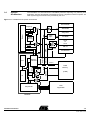
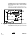
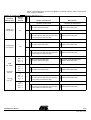
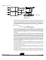
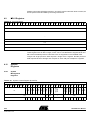
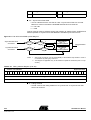
1
TSC695F
SPARC 32-bit Space Processor
User Manual
4148H-AERO-12/03
Table of Contents
Section 1
Features................................................................................................ 1-1
1.1
1.2
1.3
1.4
Description ................................................................................................1-2
Block Diagram...........................................................................................1-2
Pin Description ..........................................................................................1-2
System Architecture ..................................................................................1-5
Section 2
Architecture........................................................................................... 2-7
2.1
2.2
The RISC Machine ....................................................................................2-7
The Characteristics of RISC......................................................................2-7
2.2.1
2.3
The Advantages of RISC ....................................................................2-8
The SPARC Architecture .......................................................2-8
2.3.1
Register Windows...............................................................................2-8
Section 3
Product Description .............................................................................. 3-9
3.1
3.2
3.3
3.4
3.5
3.6
Concept.....................................................................................................3-9
Integer Unit ...............................................................................................3-9
Floating-point Unit ...................................................................................3-10
Co-processor Unit ...................................................................................3-10
Instruction Set .........................................................................................3-10
On-chip Peripherals ................................................................................3-10
3.6.1
Memory Mapping ..............................................................................3-10
3.6.2
System Registers .............................................................................3-12
3.6.3
Waitstate and Timeout Generator ....................................................3-13
3.6.4
EDAC................................................................................................3-14
3.6.5
Memory and I/O Parity......................................................................3-15
3.6.6
DMA..................................................................................................3-18
3.6.7
Traps ................................................................................................3-19
3.6.8
Timers...............................................................................................3-31
3.6.9
UARTs ..............................................................................................3-36
3.6.10 General-purpose Interface................................................................3-37
3.6.11 Execution Modes ..............................................................................3-38
3.6.12 Error Handler ....................................................................................3-39
3.6.13 Parity Checking ................................................................................3-40
3.6.14 System Clock....................................................................................3-40
3.6.15 System Availability............................................................................3-40
3.6.16 Test Mode.........................................................................................3-40
3.7
3.8
TSC695F User Manual
Test and Diagnostic Hardware Functions ...............................................3-41
Test Access Port .....................................................................................3-41
ii
4148H–AERO–12/03
Table of Contents
3.8.1
TAP Interface....................................................................................3-41
3.8.2
Board Level Architecture ..................................................................3-41
3.8.3
TAP Architecture ..............................................................................3-42
3.9
TAP Controller ........................................................................................3-42
3.9.1
TAP Controller FSM .........................................................................3-42
3.10 The Instruction Register ..........................................................................3-43
3.10.1 List of Instructions.............................................................................3-43
3.10.2 Mandatory Instructions .....................................................................3-43
3.10.3 Defined Optional Instructions ...........................................................3-44
3.10.4 Owner Instructions............................................................................3-44
3.11 Test Data Registers ................................................................................3-45
3.11.1 Bypass Register ...............................................................................3-45
3.11.2 Device ID Register............................................................................3-45
3.11.3 Boundary Scan Register...................................................................3-45
3.11.4 Checkers Scan Register...................................................................3-45
3.11.5 IU Scan Register ..............................................................................3-45
3.11.6 FPU Scan Register...........................................................................3-46
3.11.7 System Scan Register ......................................................................3-46
3.11.8 OCD Scan Register ..........................................................................3-47
3.11.9 OCD Control and Status Register ....................................................3-47
3.12 On-chip Debugger Resources ................................................................3-48
3.12.1 Hardware Breakpoints ......................................................................3-48
3.12.2 Processor Reset ...............................................................................3-49
3.12.3 Cycle Counter...................................................................................3-49
3.12.4 Freeze/Run.......................................................................................3-50
3.12.5 Step-by-step .....................................................................................3-50
Section 4
Register Descriptions.......................................................................... 4-51
4.1
4.2
4.3
4.4
4.5
4.6
4.7
4.8
4.9
4.10
IU Registers ............................................................................................4-51
Processor State Register ........................................................................4-51
Window Invalid Mask ..............................................................................4-53
Trap Base Register .................................................................................4-54
Y Register ...............................................................................................4-54
Window Registers ...................................................................................4-55
FPU Registers.........................................................................................4-57
FPU Queue Registers.............................................................................4-59
FPU f Registers.......................................................................................4-60
System Registers....................................................................................4-60
4.10.1 System Management Registers .......................................................4-60
4.11 Configuration Registers ..........................................................................4-69
iii
4148H–AERO–12/03
TSC695F User Manual
Table of Contents
4.12
4.13
4.14
4.15
Access Protection Registers ...................................................................4-77
Interrupt Registers...................................................................................4-79
Timer Registers.......................................................................................4-89
Interface Registers ..................................................................................4-93
Section 5
Signals Description ............................................................................. 5-98
5.1
5.2
5.3
5.4
5.5
5.6
TSC695F User Manual
IU and FPU Signals.................................................................................5-98
Memory and System Interface Signals .................................................5-104
Error, DMA, Halt and Check Signals.....................................................5-105
Interrupt, Clock, UART, GPI, Timer, TAP and Test Signals..................5-108
Power Signals .......................................................................................5-110
Document History..................................................................................5-110
iv
4148H–AERO–12/03
Section 1
Features
Integer Unit Based on SPARC V7 High Performance RISC Architecture
Optimized and Integrated 32/64-bit Floating-point Unit
On-chip Peripherals
– EDAC and Parity Generator and Checker
Memory Interface
– Chip Select Generator
– Waitstate Generation
– Memory Protection
DMA Arbiter
Timers:
– General-purpose Timer (GPT)
– Real-time Clock Timer (RTCT)
– Watchdog Timer (WDT)
Interrupt Controller with 5 External Inputs
General-purpose Interface (GPI)
Dual UART
Speed Optimized Code RAM Interface
8- or 40-bit Boot-pROM (Flash) Interface
IEEE 1149.1 Test Access Port (TAP) for Debugging and Test Purposes
Fully Static Design
Performance: 20 MIPs/5 MFlops (Double Precision) at SYSCLK = 25 MHz – 5V
Core Consumption: 1.5W Typ at 25 MIPs/0.7W typ. at 10 MIPs – VCC = 5V
Operating Range: 4.5V to 5.5V, –55°C to +125°C
Total Dose Radiation Capability (Parametric and Functional): 300 KRADs (Si)
SEU Event Rate Better than 1E-8 Error/Component/Day (Worst Case)
Latch-up Immunity Better than (LET) 100 MeV-cm2/mg
TSC695F User Manual
1-1
Rev. 4148H–AERO–12/03
Quality Grades: ESA SCC, QML Q or V
Package: 256 MQFPF, KGD
1.1
Description
The Rad Hard 32-bit SPARC Embedded Processor (TSC695F), ERC32 Single-chip, is a
highly integrated, high-performance 32-bit RISC embedded processor implementing the
SPARC architecture V7 specification. It has been developed with the support of the ESA
(European Space Agency), and offers a full development environment for embedded
space applications.
The processor is manufactured using the Atmel 0.5 µm radiation tolerant (≥ 300 KRADs
(Si)) CMOS enhanced process (RTP). It can operate at a low voltage for optimized
power consumption. It has been especially designed for space, as it has on-chip concurrent transient and permanent error detection.
The TSC695F includes on-chip an Integer Unit (IU), a Floating-point Unit (FPU), a Memory Controller and a DMA Arbiter. For Real-time applications, the TSC695F offers a high
security watchdog, two timer’s, an interrupt controller, Parallel and Serial interfaces.
Fault tolerance is supported using parity on internal/external buses and an EDAC on the
external data bus. The design is highly testable with the support of an On-chip Debugger (OCD), an internal and boundary scan through JTAG interface.
1.2
Block Diagram
Figure 1-1. TSC695F Block Diagram
TAP
32-bit
Integer
Unit
32/64-bit
Floating-point
Unit
Clock
and
Reset
Parity
Managt Gen./Chk.
Error
Managt
1.3
Parity
Gen./Chk.
General-purpose
Timer
Real-time Clock
Watch
Dog
Timer
General-purpose
Interface
UART B
UART A
Interrupt
Controller
GPI Bits
RxD, TxD
Interrupts
DMA
Arbiter
DMA Ctrl
Access
Controller
Mem Ctrl
Wait State
Controller
Ready/Busy
Address
Interface
Add.+Size+ASI
EDAC
Data+Check bits
Parity
Gen./Check.
Parities
Pin Description
Table 1-1. Signal Descriptions
Signal
1-2
4148H–AERO–12/03
Type
RA[31:0]
I/O
RAPAR
I/O
RASI[3:0]
I/O
Active
Description
32-bit registered address bus
High
Output buffer: 400 pF
Registered address bus parity
4-bit registered address space identifier
TSC695F User Manual
Table 1-1. Signal Descriptions (Continued)
TSC695F User Manual
Signal
Type
Active
Description
RSIZE[1:0]
I/O
RASPAR
I/O
High
Registered ASI and SIZE parity
CPAR
I/O
High
Control bus parity
D[31:0]
I/O
32-bit data bus
CB[6:0]
I/O
7-bit check-bit bus
2-bit registered bus transaction size
DPAR
I/O
High
Data bus parity
RLDSTO
I/O
High
Registered atomic load-store
Address latch enable
ALE
O
Low
DXFER
I/O
High
Data transfer
LOCK
I/O
High
Bus lock
RD
I/O
High
Read access
WE
I/O
Low
Write enable
WRT
I/O
High
Advanced write
MHOLD
O
Low
Memory bus hold
MDS
O
Low
Memory data strobe
MEXC
O
Low
Memory exception
PROM8
I
Low
Select 8-bit wide PROM
BA[1:0]
O
ROMCS
O
Low
PROM chip select
ROMWRT
I
Low
ROM write enable
MHOLD+FHOLD
+BHOLD+FCCV
Latched address used for 8-bit wide boot PROM
MEMCS[9:0] ]
O
Low
Memory chip select
MEMWR
O
Low
Memory write strobe
Output buffer: 400 pF
OE
O
Low
Memory output enable
Output buffer: 400 pF
BUFFEN
O
Low
Data buffer enable
DDIR
O
High
Data buffer direction
DDIR
O
Low
Data buffer direction
IOSEL[3:0]
O
Low
I/O chip select
IOWR
O
Low
I/O and exchange memory write strobe
EXMCS
O
Low
Exchange memory chip select
BUSRDY
I
Low
Bus ready
BUSERR
I
Low
Bus error
DMAREQ
I
Low
DMA request
DMAGNT
O
Low
DMA grant
DMAAS
I
High
DMA address strobe
DRDY
O
Low
Data ready during DMA access
IUERR
O
Low
IU error
CPUHALT
O
Low
Processor (IU and FPU) halt and freeze
SYSERR
O
Low
System error
SYSHALT
I
Low
System halt
SYSAV
O
High
System availability
NOPAR
I
Low
No parity
INULL
O
High
Integer unit nullify cycle
INST
O
High
Instruction fetch
FLUSH
O
High
FPU instruction flush
DIA
O
High
Delay instruction annulled
RTC
O
High
Real-time Clock Counter output
RxA/RxB
I
Receive data UART "A" and "B"
TxA/TxB
O
Transmit data UART "A" and "B"
Output buffer: 400 pF
Used to check the
execute stage of IU
instruction pipeline
Input trigger
1-3
4148H–AERO–12/03
Table 1-1. Signal Descriptions (Continued)
Signal
Type
GPI[7:0]
I/O
GPIINT
O
EXTINT[4:0]
I
EXTINTACK
IWDE
4148H–AERO–12/03
Description
GPI input/output
High
GPI interrupt
O
High
External interrupt acknowledge
I
High
Internal Watchdog enable
EWDINT
I
High
External Watchdog input interrupt
WDCLK
I
External interrupt
Input trigger
Input trigger
Input trigger
Watchdog clock
CLK2
I
Double frequency clock
SYSCLK
O
System clock
RESET
O
Low
Output reset
SYSRESET
I
Low
System input reset
Input trigger
TMODE[1:0]
I
Factory test mode
Functional mode=00
DEBUG
I
High
Software debug mode
TCK
I
TRST
I
Test (JTAG) reset
pull-up ≈ 37 kΩ
TMS
I
Test (JTAG) mode select
pull-up ≈ 37 kΩ
TDI
I
Test (JTAG) data input
pull-up ≈ 37 kΩ
TDO
O
Test (JTAG) data output
Test (JTAG) clock
Low
VCCI/VSSI
Main internal power
VCCO/VSSO
Output driver power
Note:
1-4
Active
If not specified, the output buffer type is 150 pF, the input buffer type is TTL.
TSC695F User Manual
1.4
System
Architecture
The TSC695F is to be used as an embedded processor requiring only memory and
application specific peripherals to be added to form a complete on-board computer. All
other system support functions are provided by the core.
Figure 1-2. TSC695F 32-bit System Architecture
DMA Unit
Boot PROM
Ax[31:0]
Xtd PROM
Master
Xchg Mem
Glue
logic
Local
Memory
Xtd RAM
I/O 0
to
I/O 3
DMAGNT
Xtd I/O
RA[31:0]
DMAAS
Memory
Interface
FPU
CB[6:0]
DPAR
DMAREQ
(BUFFEN, DDIR)
Xtd General
MEMCtrl
RAMCtrl
A[31:0]
IU
DMA
Peripherals
RAM
Memory
DMA
D[31:0]
SYSCLK
ALE
(MEMCS[9:0], MEMWR, OE)
(0 WS)
User
Application
TSC695F
TSC695F User Manual
1-5
4148H–AERO–12/03
Figure 1-3. TSC695F 8-bit System Architecture
TSC695F
Add, Data
WR, OE
ROMCS
8-bit
Boot
CS
PROM8
FPU
Memory
Interface
ROM
MEMWR, OE
(Flash Possibility)
BUFFEN, DDIR
BUSRDY
IU
Add.
decod
Note:
SRAM
8-bit bi-dir
(optional)
Peripherals
8-bit
CS
in
D[31:0]
A[31:0]
WR, OE
RA[31:0]
SYSCLK
ALE
(optional if no WS)
Xtd PROM
Area(1)
RD[7:0]
GPI[7:0]
EXTINT[4:0]
RTC
Rx, Tx
......
User
Application
1. The SRAM area is "emulated" by the extended ROM area.
This area size can be up to 15M bytes (from 0x 0100 0000 upto 0x 01EF FFFF).
This area is BUSRDY controlled for wait states.
This area is not protected by parity, neither by EDAC.
1-6
4148H–AERO–12/03
TSC695F User Manual
Section 2
Architecture
The TSC695F is a 32-bit RISC processor implementing the SPARC architecture V7
specification.
2.1
The RISC
Machine
2.2
The
Characteristics
of RISC
A Reduced Instruction Set Computer is a microprocessor designed to perform a small
number of types of computer instructions so that it can operate at a higher speed (perform more MIPS [Millions of Instructions Per Second]). The term itself (RISC) is credited
to David Petersen, a teacher at the University of California in Berkeley.
Simple instruction set – In a RISC machine, the instruction set contains simple, basic
instructions, from which more complex instructions can be composed. The instruction
set can be hardwired to speed instruction execution. No microcode is needed for
single cycle execution.
Same length instructions – Each instruction is the same length, so that it may be
fetched in a single operation.
Reduced memory access – Only load and store instructions access memory. There
are no computational instructions that access memory. Load/store instructions
operate between memory and a register. This simplifies control hardware and
minimizes the machine cycle time.
Small number of addressing modes – The instruction set uses only short
displacement, long displacement, and indexed modes to access memory.
1 machine-cycle instructions. – Most instructions complete in one machine cycle,
which allows the processor to handle several instructions at the same time. This
pipelining is a key technique used to speed up RISC machines.
Pipelining – Pipelining is a design technique where the computer’s hardware
processes more than one instruction at a time, and doesn’t wait for one instruction to
complete before starting the next. The four stages are: fetch, decode, execute, and
write. The stages are executed in parallel. As soon as one stage completes, it passes
on the result to the next stage and then begins working on another instruction.
Pipelining doesn’t improve the latency of instructions (each instruction still requires
the same amount of time to complete), but it does improve the overall throughput.
TSC695F User Manual
2-7
Rev. 4148H–AERO–12/03
Dependencies – One problem that RISC programmers face is that the processor can
be slowed down by a poor choice of instructions. Since each instruction takes some
amount of time to store its result, and several instructions are being handled at the
same time, later instructions may have to wait for the results of earlier instructions to
be stored.
However, a simple rearrangement of the instructions in a program (called Instruction
Scheduling) can remove these performance limitations from RISC programs.
2.2.1
The Advantages of
RISC
Speed – Since a simplified instruction set allows for a pipelined, the RISC processors
often achieve 2 to 4 times the performance of CISC processors using comparable
semiconductor technology and the same clock rates.
Integration – Because the instruction set of a RISC machine is so simple, it uses up
much less chip space. Extra functions, such as floating-point arithmetic unit, memory
controller, standard peripherals can also be placed on the same chip.
Software – Operating system and application programs who use the microprocessor’s
instructions will find it easier to develop code with a smaller instruction set.
The simplicity of RISC allows more freedom to choose how to use the space on a
microprocessor.
Compilers – Higher-level language compilers produce more efficient code because
they have always tended to use the smaller set of instructions to be found in a RISC
computer.
2.3
The SPARC
Architecture
The Scalable Processor Architecture is an open industry-standard architecture pioneered by SUN Microsystems in 1987.
The SPARC architecture’s definition includes the IU (Integer Unit) which is the CPU, the
FPU (Floating-point Unit) and the CP (Co-processor) which is optional. Other options
are memory controller, memory management unit and cache.
2.3.1
Register Windows
An important concept of the SPARC architecture is borrowed from the Berkeley RISC
chips. This is register windowing concept. When a program is running, it has access to
32 32-bit processor registers which include 8 global registers plus 24 registers that
belong to the current register window.
The first 8 registers in the window are called the in registers’ (i0-i7). When a function
is called, these registers may contain arguments that can be used.
The next 8 are the ’local registers’ (l0-l7) which are scratch registers that can be used
for anything while the function executes.
The last 8 registers are the ’out registers’ (o0-o7) which the function uses to pass
arguments to functions that it calls.
When one function calls another, the calling function can choose to execute a SAVE
instruction. This instruction decrements an internal counter, the current window pointer
(cwp), shifting the register window downward. The caller’s out registers then become
the calling function’s in registers, and the calling function gets a new set of local and out
registers for its own use. Only the pointer changes because the registers and return
address do not need to be stored on a stack.
The RETURN instruction acts in the opposite way.
2-8
4148H–AERO–12/03
TSC695F User Manual
Section 3
Product Description
3.1
Concept
The objective of the TSC695F is to provide a high-performance 32-bit embedded processor, with which computers for on-board embedded real-time applications can be
built. The component will be characterized by low circuit complexity and power consumption. Extensive concurrent error detection and support for fault tolerance and
reconsideration will also be emphasized. In addition to the main objective, the TSC695F
should be used for performance demanding research applications in deep space
probes. The radiation tolerance and error masking are therefore important. For the realtime applications the system might be fail-operational rather than fail-safe. By including
support for reconfiguration of the error-handling, the different demands from the applications can be optimized for the best purpose in each case.
The TSC695F will be used as a building block only requiring memory and application
specific peripherals to be added to form a complete on-board computer. All other system
support functions are provided by the TSC695F.
3.2
Integer Unit
The IU is designed for highly dependable space and military applications, and includes
support for error detection. The RISC architecture makes possible the creation of a processor that can execute instructions at a rate approaching one instruction per processor
clock.
To achieve that rate of execution, the IU employs a four-stage instruction pipeline that
permits parallel execution of multiple instructions.
Fetch – The processor outputs the instruction address to fetch the instruction.
Decode – The instruction is placed in the instruction register and is decoded. The
processor reads the operands from the register file and computes the next instruction
address.
Execute – The processor executes the instruction and saves the results in temporary
registers. Pending traps are prioritized and internal traps are taken during this stage.
Write – If no trap is taken, the processor writes the result to the destination register.
All four stages operate in parallel, working on up to four different instructions at a time. A
basic ’single-cycle’ instruction enters the pipeline and completes in four cycles.
By the time it reaches the write stage, three more instructions have entered and are
moving through the pipeline behind it. So, after the first four cycles, a single-cycle
instruction exits the pipeline and a single-cycle instruction enters the pipeline on every
TSC695F User Manual
3-9
Rev. 4148H–AERO–12/03
cycle. Of course, a ’single-cycle’ instruction actually takes four cycles to complete, but
they are called single cycle because with this type of instruction the processor can complete one instruction per cycle after the initial four-cycle delay.
3.3
Floating-point
Unit
The FPU is designed to provide execution of single and double-precision floating-point
instructions concurrently with execution of integer instructions by the IU. The FPU is
compliant to the ANSI/IEEE-754 (1985) floating-point standard.
The FPU is designed for highly dependable space and military applications, and
includes support for concurrent error detection and testability.
The FPU uses a four stage instruction pipeline consisting of fetch, decode, execute and
write stages (F, D, E and W). The fetch unit captures instructions and their addresses
from the data and address buses. The decode unit contains logic to decode the floatingpoint instruction opcodes. The execution unit handles all instruction execution. The execution unit includes a floating-point queue (FP queue), which contains stored floatingpoint operate (FPop) instructions under execution and their addresses. The execution
unit controls the load unit, the store unit, and the datapath unit. The FPU depends upon
the IU to access all addresses and control signals for memory access. Floating-point
loads and stores are executed in conjunction with the IU, which provides addresses and
control signals while the FPU supplies or stores the data. Instruction fetch for integer
and floating-point instructions is provided by the IU.
The FPU provides three types of registers: f registers, FSR, and the FP queue. The FSR
is a 32-bit status and control register. It keeps track of rounding modes, floating-point
trap types, queue status, condition codes, and various IEEE exception information. The
floating-point queue contains the floating-point instruction currently under execution,
along with its corresponding address.
3.4
Co-processor
Unit
No co-processor unit is available on TSC695F. Attempting to execute co-processor
instructions will cause the TSC695F to execute a ’cp disable’ trap (tt = 0x24).
3.5
Instruction Set
TSC695F instructions fall into six functional categories: load/store, arithmetic/logical/shift, control transfer, read/write control registers, floating-point-operate and
miscellaneous.
Note: The execution of IFLUSH will cause an ’illegal instruction’ trap (tt = 0x02).
3.6
On-chip
Peripherals
3.6.1
Memory Mapping
3-10
4148H–AERO–12/03
The TSC695F is designed to allow an easy interface to internal/external memory
resources.
TSC695F User Manual
Table 3-1. Memory Mapping
Memory
Contents
Boot
PROM
Start
Address
0x 0000
0000
Size
(bytes)
128K
→
16M
Data Size
and Parity Options
8-bit
mode
- No parity
- Only byte write
40-bit
mode
- Parity + EDAC
mandatory
- Only word write
8-bit
mode
- No parity
- Only byte write
40-bit
mode
- Parity + EDAC
mandatory
- Only word write
Access and Waitstate Control
ROMCS
MEMWR
Extended
PROM
0x 0100
0000
Max:
15M
Exchange
Memory
0x 01F0
0000
4K
→ 512K
System
Registers
0x 01F8
0000
512K
(124 used)
RAM
(8 blocks)
0x 0200
0000
8*32K
→ 8*4M
Extended
RAM
0x 0400
0000
Max:
192M
I/O Area 0
0x 1000
0000
Max: 16M
I/O Area 1
0x 1100
0000
Max: 16M
I/O Area 2
0x 1200
0000
Max: 16M
I/O Area 3
0x 1300
0000
Max: 16M
Extended
I/O Area
0x 1400
0000
Max:
1728M
Same setting as
for I/O Area 3
(no CS)
Extended
General
0x 8000
0000
Max: 2G
- No parity, no EDAC
- All data sizes allowed
(no CS)
TSC695F User Manual
- Parity + EDAC options
- Only word write
PROM8 = 0
internal
WS
generation PROM8 = 1
OE
BUFFEN
and
DDIR
(no CS)
EXMCS
- PROM8 = 0
- timeout
BUSRDY
IOWR
MEMWR
OE
BUFFEN
and DDIR
i. WS g.
and
BUSRDY
- PROM8 = 1
- BUSERR
- timeout
- BUSERR
- timeout
- Internal parity
- Only word write access
- Parity + EDAC options
- All data sizes allowed
RAMCS
[9:0]
MEMWR
internal
WS g.
/
BUFFEN
and DDIR
BUSRDY
BUSERR
OE
(no CS)
- Parity option
- No EDAC
- All data sizes allowed
/
internal
WS
generation
IOSEL
[3:0]
IOWR
OE
BUFFEN
and DDIR
and
BUSRDY
- BUSERR
- timeout
BUSRDY
IOWR
OE
BUFFEN
and DDIR
BUSRDY
/
3-11
4148H–AERO–12/03
3.6.2
System Registers
The system registers are only writable by IU in the supervisor mode or by DMA during
halt mode. All the readable registers, except UARTAR and UARTBR, can be accessed
in every access mode. UARTAR and UARTBR are only readable by IU in supervisor
mode or by DMA during halt mode. Byte or half-word store access is not allowed. A
wrong access type will generate a Memory Exception (MEXC). Only byte, half-word load
access and word access are granted.
Table 3-2. System Registers Address Map
System Register Name
Address
Read/Write Access
System Control Register
SYSCTR
0x 01F8 0000
Software Reset
SWRST
0x 01F8 0004
Supervisor W
Power-down
PDOWN
0x 01F8 0008
Supervisor W
System Fault Status Register
SYSFSR
0x 01F8 00A0
Failing Address Register
FAILAR
0x 01F8 00A4
Error and Reset Status Register
ERRRSR
0x 01F8 00B0
All R
Supervisor W
Test Control Register
TESCTR
0x 01F8 00D0
All R
Supervisor W
Memory Configuration Register
MCNFR
0x 01F8 0010
All R
Supervisor W
I/O Configuration Register
IOCNFR
0x 01F8 0014
All R
Supervisor W
Waitstate Configuration Register
WSCNFR
0x 01F8 0018
All R
Supervisor W
Access Protection Segment 1 Base Register
APS1BR
0x 01F8 0020
All R
Supervisor W
Access Protection Segment 1 End Register
APS1ER
0x 01F8 0024
All R
Supervisor W
Access Protection Segment 2 Base Register
APS2BR
0x 01F8 0028
All R
Supervisor W
Access Protection Segment 2 End Register
APS2ER
0x 01F8 002C
All R
Supervisor W
Interrupt Shape Register
INTSHR
0x 01F8 0044
All R
Supervisor W
Interrupt Pending Register
INTPDR
0x 01F8 0048
Interrupt Mask Register
INTMKR
0x 01F8 004C
Interrupt Clear Register
INTCLR
0x 01F8 0050
Interrupt Force Register
INTFCR
0x 01F8 0054
All R
Supervisor W
Watchdog Timer Register
WDOGTR
0x 01F8 0060
All R
Supervisor W
Watchdog Timer Trap Door Set
WDOGST
0x 01F8 0064
Real-time Clock Timer <Counter> Register
RTCCR
0x 01F8 0080
All R
Supervisor W
Real-time Clock Timer <Scaler> Register
RTCSR
0x 01F8 0084
All R
Supervisor W
General-purpose Timer <Counter> Register
GPTCR
0x 01F8 0088
All R
Supervisor W
General-purpose Timer <Scaler> Register
GPTSR
0x 01F8 008C
All R
Supervisor W
Timers Control Register
TIMCTR
0x 01F8 0098
All R
Supervisor W
General-purpose Interface Configuration Register
GPICNFR
0x 01F8 00A8
All R
Supervisor W
General-purpose Interface Data Register
GPIDATR
0x 01F8 00AC
All R
Supervisor W
UART ’A’ Rx and Tx Register
UARTAR
0x 01F8 00E0
3-12
4148H–AERO–12/03
All R
All R
Supervisor W
Supervisor W
All R
All R
All R
Supervisor W
Supervisor W
Supervisor W
Supervisor R/W
TSC695F User Manual
Table 3-2. System Registers Address Map (Continued)
System Register Name
Address
Read/Write Access
Supervisor R/W
UART ’B’ Rx and Tx Register
UARTBR
0x 01F8 00E4
UART Status Register
UARTSR
0x 01F8 00E8
Note:
3.6.3
All R
Supervisor W
All reserved bits have to be written with zeros in order to avoid parity error resulting in an internal error.
Waitstate and
Timeout Generator
It is possible to control the wait state generation by programming a Waitstate Configuration Register (WSCNFR). The maximum programmable number of wait-states is applied
as default at reset.
It is only possible to program the number of wait states for the following combinations:
– RAM read and RAM write
– PROM read and PROM write (i.e., EEPROM or FLASH write)
– Exchange Memory read/write
– Four individual I/O peripherals read/write
On RAM accesses, the processor will insert the programmed number of waitstates after
the first cycle.
On extended RAM accesses, one cycle is inserted at the beginning for permit an external address decoding. This area is BUSRDY controlled and no waitstate is available.
On PROM accesses, one cycle is inserted at the beginning (ROMCS is generated).
Then, the processor will apply the programmed number of waitstates after the second
cycle.
On extended PROM accesses, one cycle is inserted at the beginning for permit an
external address decoding. This area is BUSRDY controlled and no waitstate is
available.
On exchange memory accesses, the processor will sense the bus ready signal (BUSRDY) after the first two cycles of the access. If the bus ready signal is asserted at this
time the TSC695F will continue with the programmed number of waitstates. However, if
the bus ready signal is deasserted, the start of the access is put on hold. Once the BUSRDY signal is asserted again, the access will start with the programmed number of
waitstates and finish with two cycles.
On I/O area accesses, the processor will provide the programmed number of waitstates
after the first two cycles of the access. Then, the processor will sense the bus ready signal (BUSRDY). If the bus ready signal is deasserted, the access is put on hold. Once
the BUSRDY signal is asserted again, the TSC695F will continue with two cycles.
A bus timeout function of 256 system clock cycles is provided for the bus ready controlled memory areas, i.e the Extended PROM, Exchange Memory, Extended RAM,
Extended I/O and the Extended General areas. The bto bit of System Control Register is
used to select this function. The default after system reset is that the bus timeout function is enabled.
The bus timeout counter will start when the access is initiated. If the BUSRDY signal is
not asserted before a valid number of system clock cycles, a memory exception will
occur.
3.6.4
EDAC
TSC695F User Manual
The TSC695F includes a 32-bit EDAC (Error Detection And Correction). Seven bits
(CB[6:0]) are used as check bits over the data bus. The Data Bus Parity signal (DPAR)
is used to check and generate the odd parity over the 32-bit data bus. This means that
altogether 40 bits are used when the EDAC is enabled.
3-13
4148H–AERO–12/03
The TSC695F EDAC uses a seven bit Hamming code which detects any double bit error
on the 40-bit bus as a non-correctable error. In addition, the EDAC detects all bits stuckat-one and stuck-at-zero failure for any nibble in the data word as a non-correctable
error. Stuck-at-one and stuck-at-zero for all 32 bits of the data word is also detected as a
non-correctable error.
The EDAC corrects any single bit data error on the 40-bit bus. However, in order to correct any error in memory (e.g., Single Event Upset induced) the data has to be read and
re-written by software as the TSC695F does not automatically write back the corrected
data.
Figure 3-1 EDAC System Overview
data-in
trap
G
C
p data-in latch
Address
SYSYCLK
ALE
Add
Latch
Registered Address
Data
RA[31:0]
D[31:0]
G
Data Parity
G = generator
C = checker
DPAR
Check Bits in
IU
and
FPU
CB[6:0]
Hold
EDAC
MUX
Check Bits
out
NOPAR
uncorrectable
error
correctable
error
cb[6:0]
et
TEST CONTROL Reg
Interrupt Request Level Interrupt
Controller
3.6.5
Memory and I/O
Parity
The TSC695F handles parity towards memory and I/O in a special way. The processor
can be programmed to use no parity, only parity or parity and EDAC protection towards
memory and to use parity or no towards I/O.
The signal used for the parity bit is DPAR. This pin is used to check and generate the
odd parity over the 32-bit data bus according to the following table.
3-14
4148H–AERO–12/03
TSC695F User Manual
When a correctable error occurs in the RAM or exchange memory, parity is generated
even if parity is disabled.
No
Write Access
TSC695F ignores DPAR
TSC695F generates DPAR
- EDAC generates data parity
- IU (FPU) checks data parity
TSC695F ignores DPAR
0
- EDAC ignores data parity
- IU (FPU) ignores data parity but generates
its own parity for its internal usage
Yes
yes
’rpa’ = 1
’epa’ = 1
’pa x’ = 1
TSC695F User Manual
Internal
Internal
Internal
Internal
- EDAC generates data parity
- IU (FPU) checks data parity
- EDAC checks data parity
- IU (FPU) checks data parity
TSC695F ignores DPAR
0
- EDAC ignores data parity
- IU (FPU) ignores data parity but generates
its own parity for its internal usage
- EDAC checks data parity
- IU (FPU) ignores data parity but generates
its own parity for its internal usage
- IU (FPU) generates data parity
- EDAC checks data parity
TSC695F generates DPAR
TSC695F samples DPAR
0
- IU (FPU) generates data parity
- EDAC checks data parity
TSC695F generates DPAR
Internal
Internal
TSC695F samples DPAR
1
- IU (FPU) generates data parity
- EDAC ignores data parity
TSC695F generates DPAR
Internal
I/O [3:0]
Ext. I/O(3)
no
’rpa’ = 0
’epa’ = 0
’pa x’ = 0
1
Internal
Exchange
Memory
yes
’rpa’ = 1
’epa’ = 1
’pa x’ = 1
- EDAC checks parity
- IU (FPU) ignores data parity but generates
its own parity for its internal usage
- IU (FPU) generates data parity
- EDAC checks data parity
TSC695F generates DPAR
TSC695F ignores DPAR
Internal
RAM
Ext. RAM(2)
Internal
TSC695F samples DPAR
0
no
’rpa’ = 0
’epa’ = 0
’pa x’ = 0
- EDAC checks data parity
- IU (FPU) checks data parity
- IU (FPU) generates data parity
- EDAC ignores data parity
TSC695F generates DPAR
- IU (FPU) generates data parity
- EDAC ignores data parity
TSC695F generates DPAR
Internal
PROM 40-bit
Ext. PROM(1)
Internal
TSC695F samples DPAR
1
- IU (FPU) generates data parity
- EDAC checks data parity
TSC695F generates DPAR
Internal
PROM 8-bit
Ext. PROM(1)
Read or Fetch Access
Internal
1
Internal
Memory
Parity
Enabled
Internal
Accessed
Memory Area
NOPAR
Table 3-3. DPAR and NOPAR Handling (See Figure 3-1)
- IU (FPU) generates data parity
- EDAC ignores data parity
3-15
4148H–AERO–12/03
Yes
Write Access
TSC695F ignores DPAR
TSC695F doesn’t generate DPAR
- EDAC checks data parity
- IU (FPU) checks data parity
TSC695F ignores DPAR
0
- EDAC checks data parity
- IU (FPU) ignores data parity but generates
its own parity for its internal usage
No
3.6.5.1
3.6.5.2
- EDAC ignores data parity
- IU (FPU) ignores data parity but generates
its own parity for its internal usage
Internal
- IU (FPU) generates data parity
- EDAC checks data parity
TSC695F generates DPAR
Internal
0
Notes:
- EDAC generates data parity
- IU (FPU) checks data parity
- IU (FPU) generates data parity
- EDAC ignores data parity
TSC695F generates DPAR
TSC695F ignores DPAR
Internal
Extended
General
Internal
TSC695F ignores DPAR
1
- IU (FPU) generates data parity
- EDAC checks data parity
TSC695F doesn’t generate DPAR
Internal
System
Registers
Read or Fetch Access
Internal
1
Internal
Memory
Parity
Enabled
Internal
Accessed
Memory Area
NOPAR
Table 3-3. DPAR and NOPAR Handling (See Figure 3-1) (Continued)
- IU (FPU) generates data parity
- EDAC ignores data parity
1. Extended PROM area has the same configuration (memory parity enabled/disabled) than PROM area.
2. Extended RAM area has the same configuration (memory parity enabled/disabled) than RAM area.
3. Extended I/O area has the same configuration (memory parity enabled/disabled) than I/O[3] area.
Memory
Redundancy
Memory Access
Protection
3-16
4148H–AERO–12/03
Programming the Memory Configuration Register – The TSC695F provides chip
selects for two redundant memory banks for replacement of faulty banks. A memory
bank is a block composed of 32-bit data, parity and a 7-bit check-code and controlled
with one chip select signal. The size of the redundant memory banks are dependent
of the memory size register.
Unimplemented Areas – Accesses to all unimplemented memory areas are handled
by the TSC695F and detected as illegal. The memory and I/O configuration registers
define the size of memory and I/O areas. Then, if the TSC695F or the DMA Unit
access the unused area of the memory space is decoded as illegal, a memory
exception is asserted.
TSC695F User Manual
RAM Write Access Protection
Figure 3-2 RAM Write Access Protection
MEXC
Segment 1
Write
MEXC
Segment 2
Write
Segment mode (bp = 0)
RAM and Extended RAM areas
RAM and Extended RAM areas
Write
Segment 1
Write
MEXC
Segment 2
Write
MEXC
MEXC
Block mode (bp = 1)
Two segments are implemented. Each segment is defined by a Segment Base
(defined in APS1BR or APS2BR registers) and a Segment End (defined in APS1ER
or APS2ER registers).
The segment access protection can be used as a block protect function by setting
the bp bit in the System Control Register. The bp bit inverts the address criterion for
the protection function so that any access within the segment is detected.
The TSC695F can also be programmed to detect and mask write accesses (in
supervisor or/and user mode) in any part of the RAM. The protection scheme is
enabled only for data area, not for the instruction area. The programmable write
access protection is segment based.
Boot PROM Write Protection – The TSC695F supports PROM write only when it is
qualified by the external enable pin ROMWRT (ROMWRT*) and the enable bit in the
Memory Configuration Register. The TSC695F only supports byte write operations for
an 8-bit wide PROM and only word write operations for a 40-bit wide PROM.
If a write access to PROM is attempted when any of the above conditions are not
fulfilled, the System Fault Status Register and the Failing Address Register is
updated as for unimplemented area access.
3.6.6
DMA
3.6.6.1
DMA Interface
The TSC695F supports Direct Memory Access (DMA) – The DMA unit requests
access to the processor bus by asserting the DMA request signal (DMAREQ). When
the DMA unit receives the DMAGNT signal in response, the processor bus is granted.
In case the processor is in the power-down mode the processor is permanent tristated, and a DMAREQ will directly give a DMAGNT.
A memory cycle started by the processor is not interrupted by a DMA access before it
is finished.
Because the TSC695F provides registered address buses, the DMA unit must generate
such buses characteristics.
TSC695F User Manual
3-17
4148H–AERO–12/03
The TSC695F includes a DMA session timeout function preventing the DMA unit from
locking out the processor by asserting DMAREQ for more than 1024 system clock
cycles after the assertion of DMAGNT. Then, a memory exception is asserted and the
DMAGNT is removed.
3.6.6.2
Bus Arbiter
The TSC695F always has the lowest priority on the system bus and is denied access to
memory in case of a request from a DMA unit, unless the IU is performing a locked
access or after a DMA exception cycle to allow interrupt handling.
Thus the DMA is granted access to the system bus provided this has been enabled by
the processor.
3.6.7
Traps
The TSC695F supports two types of traps: synchronous and asynchronous (also called
interrupts). Synchronous traps are caused by hardware responding to a particular
instruction or by the Trap on integer condition code (Ticc) instructions; they occur during
the instruction that caused them. Asynchronous traps occur when an external event
interrupts the processor. They are not related to any particular instruction and occur
between the execution of instructions.
A trap is a vectored transfer of control to the supervisor through a special trap table that
contains the first four instructions of each trap handler. The base address of the table is
established by supervisor and the displacement, within the table, is determined by the
trap type.
Table 3-4. TSC695F – Errors, Traps and Priority Assignments
Output
Signal
Observation
Comments
Sources:
Reset
Sync.
/
1
(highest
priority)
RESET
Non-restartable,
imprecise error
Sync.
2
SYSERR
Severe error requiring a re-boot (ePC, wPC, PSR, ...)
(if unmasked) TSC695F enters (if not masked) in halt or reset mode.
Non-restartable,
precise error
IU Hardware error
Trap and/or error
Trap
Type
Sync
Async Priority (tt)
- SYSRESET pin
- OCD reset
- Software reset
- Watchdog reset
- (IU or System) error reset
2.1
0x64
Sync.
2.2
0x62
Error not removable, PC and nPC OK (dPC, WIM, TBR, ...)
TSC695F enters (if not masked) in halt or reset mode.
Register file error
Sync.
2.3
0x65
Special case (register file) of non-restartable, precise error.
TSC695F enters (if not masked) in halt or reset mode.
Restartable,
late error
Sync.
2.4
0x63
Retrying instruction but PC and nPC have to be re-adjusted (data
load, ...)
TSC695F enters (if not masked) in halt or reset mode.
Restartable,
precise error
Sync.
2.5
0x61
Retrying instruction (fetch – i.e., fPC, ...)
TSC695F enters (if not masked) in halt or reset mode.
Error mode
Sync.
3-18
4148H–AERO–12/03
IUERR
Trap occurs with et %psr bit = 0.
SYSERR
Trap ’Masked hardware errors’ if enabled.
(if unmasked) TSC695F enters (if not masked) in halt or reset mode.
TSC695F User Manual
Table 3-4. TSC695F – Errors, Traps and Priority Assignments (Continued)
Trap and/or error
Trap
Type
Sync
Async Priority (tt)
Output
Signal
Observation
Instruction access
Sync.
3
0x01
MEXC
Illegal Instruction
Sync.
4
0x02
Privileged instruction Sync.
5
0x03
FPU disabled
Sync.
6
0x04
FPU disabled by ef %psr bit = 0
Co-processor
disabled
Sync.
6
0x24
Co-processor not implemented in TSC695F
Overflow
Sync.
7
0x05
During SAVE instruction or trap taken
Underflow
Sync.
0x06
During RESTORE instruction or RETT instruction
Comments
Error on instruction fetch:
- Parity error on control bus (refer to CPAR signal description)
- Parity error on data bus (refer to DPAR signal description)
- Parity error on address bus (refer to RAPAR signal description)
- Access to protected or unimplemented area
- Uncorrectable error in memory (refer to “EDAC” section)
- Bus time out (refer to “Waitstate and Timeout Generator” section)
- Bus error (refer to BUSERR* signal description)
Window
FPU exception
Memory add. not
aligned
Sync.
8
0x07
Non-restartable
error
Sync.
9.1
Data bus error
Sync.
9.2
Parity error on FPU data bus.
Restartable error
Sync.
9.3
Can be removed by restarting the instruction.
Sequence error
Sync.
9.4
Identified by f t t %psr field = 4
Unimplemented
FPop
Sync.
9.5
Identified by f t t %psr field = 3
IEEE exceptions:
Sync.
9.6
Identified by cexc field with field f t t = 1:
- Invalid operation
- Division by zero
- Overflow/Underflow
- Inexact
Unfinished FPop
Sync.
Data access
TSC695F User Manual
Sync.
9
0x08
Severe error, cannot restart the instruction.
Never asserted. No trap nor error
10
0x09
MEXC
Error on data load:
- Parity error on control bus (refer to CPAR signal description)
- Parity error on data bus (refer to DPAR signal description)
- Parity error on address bus (refer to RAPAR signal description)
- Access to protected or unimplemented area
- Uncorrectable error in memory (refer to “EDAC” section)
- Bus time out (refer to “Waitstate and Timeout Generator” section)
- Bus error (refer to BUSERR* signal description)
- System register access violation
3-19
4148H–AERO–12/03
Table 3-4. TSC695F – Errors, Traps and Priority Assignments (Continued)
Output
Signal
Observation
Trap and/or error
Trap
Type
Sync
Async Priority (tt)
Tag overflow
Sync.
11
0x0A
TADDccTV and TSUBccTV instructions
Trap instructions
Sync.
12
0x80
to
0xFF
Trap on integer condition codes (Ticc)
System hardware
error
Sync.
Watchdog timeout
Async. 13
0x1F
External INT 4
Async. 14
0x1E
Comments
SYSERR
Parity error on system registers
(if unmasked) Trap ’Masked hardware errors’ if enabled.
EXTINTAK
INT level=15
No-maskable – Internal or external (EWDINT pin)
INT level=14
EXTINTAK on only one of EXTINT[4:0]
Real time clock timer Async. 15
0x1D RTC
INT level=13
General-purpose
timer
Async. 16
0x1C
INT level=12
External INT 3
Async. 17
0x1B
EXTINTAK
INT level=11
EXTINTAK on only one of EXTINT[4:0]
External INT 2
Async. 18
0x1A
EXTINTAK
INT level=10
EXTINTAK on only one of EXTINT[4:0]
DMA timeout
Async. 19
0x19
INT level=9
DMA session exceeds permitted time
DMA access error
Async. 20
0x18
INT level=8
DMA performs an access error, access violation or
illegal access
UART Error
Async. 21
0x17
INT level=7
Correctable memory
error
Async. 22
0x16
INT level=6
EDAC detects and corrects an error. Data read OK
but source (memory contents) not updated.
UARTB - Data
ready
- Trans.
ready
Async. 23
0x15
INT level=5
Generated by the UARTs each time a data word has
been correctly received or/and sent
UARTA - Data
ready
- Trans.
ready
Async. 24
0x14
INT level=4
External INT 1
Async. 25
0x13
EXTINTAK
INT level=3
EXTINTAK on only one of EXTINT[4:0]
External INT 0
Async. 26
0x12
EXTINTAK
INT level=2
EXTINTAK on only one of EXTINT[4:0]
Masked hardware
errors
Async. 27
(lowest
priority)
0x11
IUERR (if IU
error mode)
INT level=1
When a hardware error is set in the Error and Reset
Status Register and the error is masked.
It is the OR of :
- IU hardware error masked
- IU error mode masked
- System hardware error masked
When synchronous traps and asynchronous traps occur in the same cycle, the synchronous trap with the highest priority is taken and other synchronous traps (with lower
priority) are ignored. At the same time, the asynchronous traps are reported as pending
in the ‘interrupt pending’ register. Once the synchronous trap with the highest priority is
3-20
4148H–AERO–12/03
TSC695F User Manual
handled, the unmasked asynchronous traps are handled ( from the highest priority to the
lowest priority).
If a synchronous trap event occurs during memory access, the System Fault Status register is updated in accordance with the synchronous condition table (see table 3-5). The
System Fault Status register (SYSFSR) also indicates the type of error and whether this
type of error is valid. At the same time, the failing address is stored in the Failing
Address Register (FAILAR).
Table 3-5. SYSFSR & FAILAR Update -synchronous condition table
Synchronous
Fault Type
Instruction access
Data access
SYSFSR
FAILAR
SYSFSR
FAILAR
parity error on control bus
N
U
U
U
parity error on data bus
N
U
U
U
parity error on address bus
N
U
U
U
access to protected area
N
U
U
U
access to unimplemented area
N
U
U
U
system registers parity error
N
U
U
U
system registers access violation
N
U
U
U
uncorrectable error in memory
N
U
U
U
bus timeout
N
U
U
U
bus error
N
U
U
U
Note:
U means that the register is updated
N means that the register is not updated
If an asynchronous trap event occurs, the System Fault Status register is updated and
reflects the type of error in accordance with the asynchronous condition table (refer to
table 3-6). The System Fault Status register (SYSFSR) also indicates whether the type
of error is valid. At the same time, the failing address is stored in the Failing Address
Register (FAILAR) in accordance with the table 3-6.
An asynchronous fault can only update SYSFSR (and FAILAR) if none of the synchronous and asynchronous fault valid bit is set in SYSFSR. In case one of the fault valid
bits is set, a trap is generated but information in the SYSFSR and FAILAR are irrelevant.
TSC695F User Manual
3-21
4148H–AERO–12/03
Table 3-6. SYSFSR & FAILAR Update -asynchronous condition table
Asynchronous Fault Type
SYSFSR
FAILAR
Watchdog timeout
U
N
External INT 4
N
N
Real time clock timer
N
N
General-purpose timer
N
N
External INT 3
N
N
External INT 2
N
N
DMA timeout
U
N
DMA access error
U
U
UART Error
U
N
Correctable memory error
U
U
UARTB
N
N
UARTA
N
N
External INT 1
N
N
External INT 0
N
N
Masked hardware errors
N
N
Note:
U means that the register is updated
N means that the register is not updated
The fault valid bits are reset by writing any value to the SYSFSR register. The register is
set to the value 0x00000078 (reset value).
3.6.7.1
Synchronous Traps
Reset – The reset trap is a special case of the external asynchronous trap type. It is
asynchronous because it is triggered by asserting the RESET input signal. But from
that point on, its behavior is entirely different from that of an asynchronous interrupt.
As soon as the IU recognizes the RESET signal, it enters reset mode (Reset Mode)
and stays there until the RESET line is deasserted. The processor then enters
execute mode and then the execute trap procedure. Here, it deviates from the normal
action of a trap by modifying the enable traps bit (et = 0), and the supervisor bit (s =
1). It then sets the PC to 0 (rather than changing the contents of the TBR), the nPC to
4, and transfers control to location 0.
All other PSR fields, and all other registers retain their values from the last execute
mode (upon power-up reset the state of all registers other than the PSR are
undefined).
If the processor got to reset mode from error mode, then the normal actions of a trap
have already been performed, including setting the tt field to reflect the cause of the
error mode. Because this field is not changed by the reset trap, a post-mortem can be
conducted on what caused the error mode. The processor enters error mode
3-22
4148H–AERO–12/03
TSC695F User Manual
whenever a synchronous trap occurs while traps are disabled.
Hardware error – When a hardware error is detected, the trap handling routine saves
the error information sampled in the Error and Reset Status Register.
The trap routine then resumes the instruction by returning from the trap routine. If the
cause of the error was a transient fault, it may be removed by just resuming the
instruction. If the error was caused by a fault that is not removable by resuming the
instruction, another hardware error trap is generated and the trap handling routine
propagates the error to a higher level of the application.
If the fault is in a critical register or latch which the trap handling routine uses, another
hardware error trap is generated. A synchronous trap during the time when traps are
disabled is a critical error and the TSC695F enters the error mode and halts. This
means that the error detection mechanism has to detect the error when the faulty
instruction is in the execute stage in order to handle the trap normally, i.e.,, correct PC
for the faulty instruction.
Instruction access – An instruction access exception trap is generated if a memory
exception occurs (MEXC signal is asserted) during an instruction fetch.
Illegal instruction
An illegal instruction trap occurs:
–
When the UNIMP instruction is encountered,
–
When an unimplemented instruction is encountered (excluding FPops and
CPops),
–
In any of the situations below where the continued execution of an
instruction would result in an illegal processor state:
1. Writing a value to the %psr’s cwp field that is greater than the number of
implemented windows (with WRPSR assembly instruction)
2. Executing an Alternate Space instruction with its i bit set to 1
3. Executing a RETT instruction with traps enabled (et = 1)
4. Executing an IFLUSH instruction
Unimplemented floating-point instructions do not generate an illegal instruction trap.
They generate FPU exception. Floating-point instructions are coded with: op = 10
and op3 = 11010x.
Privileged instruction – This trap occurs when a privileged instruction is encountered
while the PSR’s supervisor bit is reset (s = 0).
FPU disabled – A FPU disabled trap is generated when an FPop, FBfcc, or floatingpoint load/store instruction is encountered while the PSR’s ef bit = 0.
Coprocessor disabled – A coprocessor disabled trap is generated when a CPop,
CBccc, or coprocessor load/store instruction is encountered.
Window overflow – This trap occurs when the continued execution of a SAVE
instruction would cause the cwp to point to a window marked invalid in the WIM
register.
Window underflow – This trap occurs when the continued execution of a RESTORE
instruction would cause the cwp to point to a window marked invalid in the WIM
register. The window underflow trap type can also be set in the %psr during a RETT
instruction, but the trap taken is a reset.
TSC695F User Manual
3-23
4148H–AERO–12/03
Memory address not aligned – Memory address not aligned trap occurs when a load
or store instruction generates a memory address that is not properly aligned for the
data type or if a JMPL instruction generates a PC value that is not word aligned (loworder two bits nonzero).
FPU exception
– Non-restartable error (%fsr’s f t t field = 7)
This type of error concerns parity errors that were detected after the state of the
FPU was changed and could not be removed by restarting the instruction (%fsr,
Register File,...).
An hardware error will be asserted and stay asserted until the next FPop encountered in the instruction stream (after a STDFQ instruction) modifies the ftt field of
%fsr.
–
Data bus error (%fsr’s f t t field = 5)
This type of error concerns parity errors on the internal data bus detected by the
FPU.
–
Restartable error (%fsr’s f t t field = 6)
This type of error concerns parity errors in the FPU that were detected before
changing the FPU state and could be removed by restarting the instruction (IU to
FPU internal control bus, ...).
–
Sequence error (%fsr’s f t t field = 4)
This exception is asserted by the FPU when a floating-point instruction (other than
FP store) is attempted after the FPU has entered either pending exception or exception mode. The FPU suspends all instruction execution with the exception of FP
stores until the FP exception has been acknowledged and the FP queue has been
cleared.
–
Unimplemented FPop (%fsr’s f t t field = 3)
This exception is asserted by the FPU upon encountering a defined SPARC FPop
instruction that is not supported by the TSC695F. This includes all operations using
extended-precision format operands. The trap handler is expected to emulate the
unimplemented instruction.
–
IEEE exceptions (%fsr’s f t t field = 1)
This class of exceptions is defined as part of the IEEE-754 Standard. The five
exceptions defined as IEEE Exceptions are reported in the cexc field and accumulated in the aexc field of the %fsr. The only exceptions that can coincide are inexact
with overflow and inexact with underflow.
Invalid Operation (%fsr’s cexc field = 10000b) – The invalid operation exception is
signaled if an operand is invalid for the operation to be performed. The result, when
the exception occurs without a trap, shall be a quiet NaN provided the destination has
a floating-point format. The invalid operations are
– Any operation on a signaling NaN,
– Addition or subtraction: Magnitude subtraction of infinities such as (+ ∞) + (-∞),
– Multiplication: 0 x ∞,
– Division: 0/0 or ∞/∞,
– Square root if the operand is less than zero,
– Conversion of a binary floating-point number to an integer or decimal format
when overflow. infinity, or NaN precludes a faithful representation in that
format and this cannot otherwise be signaled,
3-24
4148H–AERO–12/03
TSC695F User Manual
– Floating-point compare operations: when one or more of the operands are
NaN.
Division-by-zero (%fsr’s cexc field = 00010b) –
If the divisor is zero and the dividend is a
finite nonzero number, then the division by zero exception shall be signaled. The result, when
no trap occurs, shall be a correctly signed ∞.
Overflow (%fsr’s cexc field = 0100xb) – The exceeded in magnitude by what would have
been the rounded floating-point result were the exponent range unbounded. The
result, when no trap occurs, shall be determined by the rounding mode and the sign
of the intermediate result as follows:
– Round to nearest carries all overflows to ∞ with the sign of the intermediate result,
– Round toward 0 carries all overflows to the format’s largest finite number with
the sign of the intermediate result,
– Round toward –∞ carries positive overflows to the format’s largest positive finite
number, and carries negative overflows to –∞,
– Round toward + ∞ carries negative overflows to the format’s most negative finite
number, and carries positive overflows to +∞.
Underflow (%fsr’s cexc field = 0010xb) – The TSC695F’s FPU asserts an underflow
exception when the rounded result is inexact and would be smaller in magnitude than
the smallest normalized number in the specified format.
Inexact (%fsr’s cexc field = 0xx01b) – The inexact exception is generated whenever there
is a loss of accuracy (or significance) in the result. The TSC695F’s FPU computes
results to higher precision than the number of fraction bits in the format. If any of the
fraction bits to the right of the LSB was one prior to rounding, the inexact exception is
signaled.
Unfinished FPop
– The TSC695F’s FPU never asserts this exception since all implemented
instructions are executed within hardware.
– Data access exception
A data access exception trap is generated if a parity error, uncorrectable EDAC
error, access violation, bus timeout or system bus error is detected (MEXC signal is
asserted) during the data cycle of any instruction that moves data to or from
memory.
– Tag overflow
This trap occurs if execution of a TADDccTV or TSUBccTV instruction causes the
overflow bit of the integer condition codes to be set. See the instruction definitions of
TADDccTV and TSUBccTV for details.
– Trap instructions
This trap occurs when a Ticc instruction is executed and the trap conditions are met.
There are 128 programmable trap types available within the trap instruction trap.
See SPARC V7.0 Instruction Set, Ticc instruction for details.
3.6.7.2
Interrupts or
Asynchronous
Traps
TSC695F User Manual
The TSC695F handles 15 asynchronous traps.
It is possible to mask each individual interrupt (except for interrupt 15 – watch-dog) by
setting the corresponding bit in the Interrupt Mask Register (INTMKR). The Interrupt
Pending Register (INTPDR) reflects the pending interrupts. It is possible to clear pending interrupts by setting the corresponding bit in the Interrupt Clear Register (INTCLR).
3-25
4148H–AERO–12/03
The interrupts in the Interrupt Pending Register (INTPDR) are cleared automatically
when the interrupt is acknowledged.
By programming the Interrupt Shape Register (INTSHR), it is possible to define the
external interrupts to be either active low or active high and to define the external interrupts to be either edge or level sensitive. Also, by programming the Interrupt Shape
Register (INTSHR), it is possible to make one of the external interrupts generate a pulse
on the EXTINTACK output when the IU acknowledges the interrupt.
Edge sensitive interrupts will be detected only when a transition occurs.
Level sensitive interrupts will be detected as long as the interrupt line is asserted. When
the interrupt line is deasserted, the corresponding bit in Interrupt Pending Register
(INTPDR) will be cleared
Figure 3-3 Interrupt System Overview
The external interrupt input is filtered only if it is active for at least 2 SYSCLK.
The interrupts in the INTPDR register are
cleared automatically when the interrupt is
acknowledged (INTACK).
EXTINTACK
INTSHR
EXTINT[4:0]
Reg.
5
Shape
5
Maskable Internal Interrupts
Internal
Watchdog
9
1
0
EWDINT
INTMKR
Reg.
INTPDR
5
Glitch
removal
5
14
15
≥1
15 Prior
and
15
4
Interrupt Request
Level to IU
Reg.
15
INTFCR
Reg.
it
(bit 19)
TESCTR
Reg.
15
IWDE
Reg.
Reg.
INTCLR
SYSCTR
INTACK from IU
When ’Interrupt test’ (it) is not enabled:
– Setting or clearing a bit in INTFCR register will only affect INTFCR register.
The corresponding interrupt will not be forced.
– When the interrupt is acknowledged, the TSC695F will automatically clear the
corresponding bit in the INTPDR register.
When ’Interrupt test’ (it) is enabled:
– Setting a bit in INTFCR register will force the corresponding interrupt if it is not
masked in INTMKR register.
– When the interrupt is acknowledged, the TSC695F will automatically clear the
corresponding bit in the INTFCR register if this bit is set, otherwise it will clear
the corresponding bit in the INTPDR register. In this way no external interrupts
are lost.
3-26
4148H–AERO–12/03
TSC695F User Manual
3.6.8
Timers
In software debug mode the timers are controlled by a system register bit (phlt – bit 4 in
Timer Control Register – TIMCTR) and an external pin (DEBUG). Setting the external
pin IWDE to VCC enables the Watchdog Timer. Otherwise the watchdog function must
be externally provided.
While the halt mode is active, the timers are temporary halted.
Figure 3-4 Timers Halt
31
15
0
SYSCTR – (System Control Register)
IWDE
reset
Watchdog
Timer
gpt int
RTC
rtc int
3.6.8.1
DEBUG
Watchdog Clock
clk
General
Purpose
Timer
Real
Time
Clock
Timer
General-purpose
Timer
clk
enable
clk
SYSCLK
31
clk
enable
7 6
UARTB Halt
UARTA Halt
Peripherals Halt
clk
5
4 3
0
TIMCTR
(Timer Control Register)
ph
lt
wd int
clk
enable
The General-purpose Timer (GPT) provides, in addition to a generalized counter function, a mechanism for setting the step size in which actual time counts are performed (a
two-stage counter). This timer/counter pulse generator consists of two parts:
pre-SCALER (GPTSR): it is a counter to adjust the step size in which counter does
the actual time count.
COUNTER (GPTCR): it is a counter to actually count time in steps as set by the value
in scaler. The counter is decremented when the scaler reaches zero.
Figure 1. GPT Implementation
Set
Preload
Cnt.
SYSCLK
Set
Preload
Cnt.
16-bit Scaler
zero
indication
GPT
Interrupt
32-bit Counter
Control
[enable, (periph_halt•DEBUG), load, re-load, hold, stop at zero]
GPT is clocked by the internal system clock. The timer is programmable by writing to the
Timer Control Register (TIMCTR). They are possible to program to be either of singleshot type or periodical type and in both cases generate an interrupt when the delay time
TSC695F User Manual
3-27
4148H–AERO–12/03
has elapsed. If the timer is not programmed with a new value when set to periodical
type, it restarts from the latest programmed value and continue to count down, thus generating interrupts periodically. It is possible to halt and restart the timers by writing to the
Timer Control Register (TIMCTR).
Only the current value of the scaler and counter of the GPT can be read, never the preloaded values.
After system reset the Real-time Clock is not running and must be programmed as
required.
Programming
if
scaler > 0
if
then
scaler = 0
Do
not
counter × ( scaler + 1 )
Timeout = --------------------------------------------------------SYSCLK
counter
+ 1then
Timeout = ----------------------------SYSCLK
program
counter = 0
Behavior – During the ‘1’ –> ‘0’
transition, the counter has the value of ‘0’ for one
clock cycle and then immediately reloaded. The timeout period is not affected, the
reloaded value will be decremented on the next scaler tick as can be expected and
generates a timeout period equal to the reload value.
When the scaler is rogrammed to ‘0’, a scaler tick is generated every clock, and the
timeout period will be the counter reload value + 1.
Figure 3-5 Timer Behavior Example when Scaler > 0
Reload mode, Scaler = 1, Counter = 3
SYSCLK
Scaler Tick
Counter Value
1
0
3
2
1
0
3
1
0
2
Internal INT
Counter x (Scaler+1)
Timeout
Figure 3-6 Timer Behavior Example when Scaler = 0
Reload mode, Scaler = 0, Counter = 3
SYSCLK
Scaler Tick
Counter Value
1
0
3
2
1
0
3
2
3
Internal INT
Timeout
3-28
4148H–AERO–12/03
Counter+1
Counter+1
TSC695F User Manual
Figure 3-7 Timer Behavior Example when Counter = 0
Initialization of Reload mode, Scaler = 1, Counter = 0
SYSCLK
Scaler Tick
Counter Value
xx(*)
0
reloading with ’0’
2
Only one INT located during the
loading if previous value ≠ 0
Internal INT
load and start command
(*) after reset, counter value = 0xFFFFFFFF
3.6.8.2
Real-time Clock
Timer
The only functional differences between the two timers are that the Real-time Clock
Timer (RTCT) has an 8-bit scaler (16-bit scaler for GPT) and that the RTCT interrupt has
higher priority than the GPT interrupt.
RTCT information is available on RTC output pin during 1.5 SYSCLK period.
Figure 3-8 RTCT Implementation
Set
Preload
Cnt.
SYSCLK
Set
Preload
Cnt.
8-bit Scaler
zero
indication
32-bit Counter
RTC
output pin
RTC
Interrupt
Control
[enable, (periph_halt•DEBUG), load, re-load, hold, stop at zero]
Figure 3-9 RTC Pin Functionality
SYSCLK
RTC
(counter = 1, scaler = 3)
or (counter = 2, scaler = 1)
RTC
(counter = 1, scaler = 2)
or (counter = 2, scaler = 0)
RTC
(counter = 1, scaler = 1 or 0)
3.6.8.3
Watchdog Timer
The watchdog is supplied from a separate external input (WDCLK pin) which must have
a frequency which is at least three times lower than SYSCLK. This input is divided by 16
in a prescaler or routed directly to the scaler of the watchdog as set in the System Control Register (wdcs bit in SYSCTR).
The Watchdog Timer Register (WDOGTR) holds the loaded value both in the scaler and
in the counter of the watchdog timer.
TSC695F User Manual
3-29
4148H–AERO–12/03
System/processor RESET
Figure 3-10 Watchdog Timer States and Transitions
WD Program (new value)
WD Init
Trap Door
Set
WD Program
(new value)
WD Disabled
WD Enabled
WD Timeout
Acknowledge
(new value)
Reset
Timeout
WD
WD
Reset Timer
Halted
Enabled
WD Timeout
WD Timeout
Trap Door Set
WD Program
(refresh)
Interrupt
Processor
RESET
After reset, the timer is enabled and starts running. The default value is the scaler set to
maximum and the counter set to maximum. By writing to the Trap Door Set (WDOGST)
after system reset, the timer can be disabled. After, a write operation to the Watchdog
Timer Register (WDOGTR) starts the timer counting with the value of the Watchdog
Timer Register. Note that the Watchdog cannot be disabled once the Watchdog Timer
Register (WDOGTR) has been written.
If the timer is refreshed by writing to Watchdog Timer Register (WDOGTR) before the
counter reaches zero value, the timer restarts the counting with the new delay value. If
the timer is not refreshed (reprogrammed) before the counter reaches zero value, an
interrupt is sent. Simultaneously, the timer starts counting a reset timeout period with the
programmed delay time. Then, if the timer is acknowledged by writing to Watchdog
Timer Register (WDOGTR) with a new programmed value before the reset timeout
period elapses again, the timer restarts counting with the new delay value, but if the
timer is not acknowledged before the reset timeout period elapses, a reset is applied.
This updates the rstc field in the Error and Reset Status Register (ERRRSR).
Programming:
Timeout = 16
wdcs (----------------------------------------------------------------------scaler + 1 ) × ( counter + 1 )×
WDCLK
ResetTimeout = Timeout + 16
3.6.9
UARTs
wdcs (------------------------------------------------------------------------------------scaler + 1 ) × ( resetcounter + 1 )
×
WDCLK
Two full duplex asynchronous receiver transmitters (UART) are included.
In software debug mode the UARTs are controlled by Timer Control Register bits (phlt,
ahlt and bhlt – respectively bit 4/5/6 in TIMCTR) and an external pin (DEBUG).
While the halt mode is active, the UARTs are temporarily halted.
3-30
4148H–AERO–12/03
TSC695F User Manual
Figure 3-11 UARTs Halt
TxA
UART
’A’
clk
RxA
TxB
UART
’B’
RxB
DEBUG
clk
enable
UARTs Clock
clk
enable
clk
7 6
5
4 3
0
TIMCTR
(Timer Control Register)
bh
lt
ah
lt
ph
lt
31
UARTB Halt
UARTA Halt
Peripherals Halt
The data format of the UARTs is eight bits. It is possible to choose between even or odd
parity, or no parity, and between one and two stop bits by programming the System
Control Register (SYSCTR). After system reset odd parity and one stop bit are set. The
baud rate of the UART is set by programming scaler (us) and ubr fields the System Control Register (SYSCTR). After system reset the baud rate is set to fSYSCLK divided by 32.
Programming
Clock
-–1
Scaler ( us ) = -------------------------------------------------------------------32 × BaudRate × 〈 2 – ubr〉
The UARTs provide double buffering, i.e., each UART consists of a transmitter holding
register, a receiver holding register, a transmitter shift register, and a receiver shift register. Each of these registers are 8-bit wide. For each UART a RX and TX Register is
provided (UARTAR and UARTBR). There is also a common UART Status Register
(UARTSR).
To output a byte on the serial output the following procedure should be followed. First,
the UART Status Register (UARTSR) should be read in order to check that the transmitter holding register (thea and theb) is empty. Otherwise, the previous byte to be output
may be lost (note that the tse bit is not useful for the purpose of checking if a character
may be written to the Rx and Tx register). Then, the byte to be output is written in the Rx
and Tx register (UARTAR and UARTBR). The byte written will then automatically be
transferred to the transmitter send register and converted to serial form also adding start
bit, parity bit, and stop bit(s). The above described sequence can be part of a trap handler for the UART interrupt.
A correctly received byte is indicated by the Data Ready bit (dra or drb) in the UART status register (UARTSR). In case of error (framing error, stop bit error, parity error or
overrun error), the respective bits fe, pe, and oe are set in the UART status register
(UARTSR) but not dra or drb bit.
The UARTs generate an interrupt each time a byte has been received or a byte has
been sent. There is another interrupt to indicate errors, but this interrupt is common for
both UART channels.
The UART uses an internal clock which is 16 times faster than the baud-rate, and samples each bit 16 times, to ensure error free reception. The clock is derived either from
the system clock (SYSCLK) or can use the watchdog clock (WDCLK). This is done by
TSC695F User Manual
3-31
4148H–AERO–12/03
programming ucs bit in System Control Register – SYSCTR. If WDCLK input is chosen,
its frequency must be at least 3 times less than SYSCLK frequency.
The external UART interfaces consist of transmit data output (TxA and TxB) and receive
data input (RxA and RxB). Note that no hardware handshake signals, such as CTS or
RTS are implemented. Any handshaking must be implemented in software (e.g. using
XON/XOFF).
3.6.10
General-purpose
Interface
The General-purpose Interface (GPI) is an 8-bit parallel I/O port. Each pin can be configured as an input or an output thanks to the GPI Configuration Register (GPICNFR).
When a pin is an input, its state is read from GPI Data Register (GPIDATR). When a pin
is an output, its state corresponds to the bit value written in GPI Data Register (GPIDATR), this value can be re-read in GPI Data Register (GPIDATR).
An edge detection is made on selected GPI inputs. Falling or rising edge is chosen in
GPI Configuration Register (GPICNFR). Every input transition on GPI generates an
external positive pulse on GPIINT pin of two SYSCLK width.
Figure 3-12 General-purpose Interface
R/F[i] (of GPI Configuration Register- GPICNFR)
I/O[i] (of GPI Configuration Register- GPICNFR)
or
Detection
Glitch
Removal
2 x SYSCLK
GPIINT
GPID [i] (of GPI Data Register
– GPIDATR)
GPI [i]
I/O[i] (of GPI Configuration Register
– GPICNFR)
Write to GPI Data Register
– GPIDATR
After Reset, all GPI I/O are configured as inputs.
3.6.11
Execution Modes
3.6.11.1 Reset Mode
When the SYSRES input is asserted, the TSC695F issues a reset of itself and asserts
the RESET output which is intended to be used as a reset signal to all other components in the system. This RESET output has a minimum of 1024 SYCLK width to allow
the usage of flash memories.
After the assertion of SYSRES, the processor starts in the ’reset mode’, resetting all
system registers.
Reset mode is also entered when the RESET output is asserted from any other reason
than SYSRES.
– Software reset which is caused by the software writing to a Software Reset
Register.
– OCD reset.
– Watchdog reset which is caused by a Watchdog reset timeout.
– Error reset which is caused by a hardware parity error or an IU error mode.
Error and Reset Status Register contains the source of the last processor reset. OCD
reset is seen as SYSRES assertion.
3.6.11.2 Run Mode
3-32
4148H–AERO–12/03
In this mode the IU/FPU is executing, all peripherals are running (if software enabled).
TSC695F User Manual
3.6.11.3 System Halt Mode
System Halt mode is entered when the SYSHALT input is asserted. The CPUHALT output is asserted, freezing IU/FPU execution. All timers are halted and the UART
operation is stopped. When SYSHALT is deasserted, the previous mode is entered.
DMA accesses are allowed during system halt mode, in which DMA has permanent
access to the system, i.e.,, DMAGNT is asserted immediately on DMAREQ.
3.6.11.4 Power-down Mode
This mode is entered by writing to the Power-down Register (PDOWN). Then the bus
arbiter removes the bus ownership from the IU. prd bit in the System Control Register
(SYSCTR) must be programmed prior to entering power-down mode.
DMA accesses are allowed during power-down mode.
The TSC695F leaves the power-down mode if an external interrupt is asserted.
3.6.11.5 Error Halt Mode
Error Halt mode is entered under the following circumstances:
–
A internal hardware parity error.
–
The IU enters error mode.
In Error Halt mode, the CPUHALT and SYSERR outputs are asserted (note that
SYSERR is also asserted if a masked error occurs even though Error Halt mode is not
entered in this case). All timers are halted and the UART operation is stopped in this
mode. The only way to exit Error Halt Mode is through Cold Reset by asserting
SYSRESET.
The TSC695F allows DMA accesses during error halt mode.
3.6.12
Error Handler
TSC695F User Manual
The TSC695F has one error output signal (SYSERR) which indicates that an unmasked
error has occurred. Any error signalled on the error inputs from the IU and the FPU is
latched and reflected in the Error and Reset Status Register (ERRRSR). It is possible to
program an error mask in the System Control Register (SYSCTR) for each type of error
(excepted for FPU) in order to determine whether the specific error shall lead to the processor ignoring the error or asserting a processor halt or processor reset (programming
the System Control Register – SYSCTR). As default, an error leads to a processor halt.
All unmasked errors, asserts the SYSERR pin and this pin is asserted until all the
unmasked error bits in the Error and Reset Status Register (ERRRSR) are cleared.
3-33
4148H–AERO–12/03
Figure 3-13 Error Handler Schematic
IUERR pin
IU
register
file
checkers
async.
Trap 0x65
Or
Trap 0x61
Trap 0x62
Trap 0x63
Trap 0x64
IU Error Mode
other
sources
internal
parity
checkers
iuem
(trap in trap)
error mode
IU Hardware
Error
FPU Hardware
Error
MEXC pin
trap
handler
synch.
Memory Exception
Interrupt Request Level [3:0]
Interrupt Acknowledge
internal
parity
checkers
FPU
3.6.13
Parity Checking
or
Trap
0x08
other
sources
register
file
checkers
iuhe
fpuhe
system
hardware
error
syshe
ERRRSR
memory
control
iuemmsk
rhiuem
iuhemsk
rhiuhe
syshemsk
rhsyshe
interrupt
system
EXINT[4:0]
pins
and
Masked
HW error
SYSERR pin
other
sources
SYSCTR
and
or
RESET HALT
System
The TSC695F includes parity checking and generation if required on the external data
bus (DPAR pin). It includes parity checking on the external address bus (RAPAR pin). It
also includes parity checking on ASI and SIZE (RASPAR pin) together with parity generation and checking on all system registers. The TSC695F also includes parity
generation and checking on the internal control bus to the IU (CPAR pin). If a parity error
is detected on the external data bus, the external address, the external RASI and
RSIZE, the internal control bus, a memory exception is asserted. If a memory exception
event occurs the System Fault Status Register (SYSFSR) is updated and reflects the
type and location of parity errors.
All external parity checking can be disabled using the NOPAR signal.
3.6.14
System Clock
The TSC695F uses CLK2 clock input directly and creates a system clock signal by
dividing CLK2 by two. It drives SYSCLK pin with a nominal 50% duty cycle for the application. Some output signals are clocked by the CLK2 negative edge which means that
the CLK2 duty cycle has a direct impact on the system performance.
When interfacing peripherals (I/O interface, DMA interface, etc.) it is highly recommended that only SYSCLK rising edge is used as reference as far as possible.
3.6.15
System Availability
The sysav bit in the Error and Reset Status Register (ERRRSR) can be used by software to indicate system availability. The sysav bit is cleared by reset and is
programmable by software. Note that the SYSAV output signal is asserted only if the
sysav bit is set and SYSERR is deasserted, i.e., no error has been detected.
3.6.16
Test Mode
The TSC695F includes a number of software test facilities such as EDAC test, Parity
test, Interrupt test, Error test and a simple Test Access Port. These test functions are
controlled using the Test Control Register (TESCTR).
Note that TMode[1:0] pins are only dedicated for factory test. These pins must be kept
grounded.
3-34
4148H–AERO–12/03
TSC695F User Manual
3.7
Test and
Diagnostic
Hardware
Functions
3.8
Test Access Port
3.8.1
TAP Interface
A variety of TSC695F test and diagnostic hardware functions, including boundary scan,
internal scan, clock control and On-chip Debugger, are controlled through an IEEE
1149.1 (JTAG) standard Test Access Port (TAP). Commands and data are sent as
serial data between the JTAG master and the TSC695F (a JTAG slave), via a 4 wire
serial testability bus (JTAG bus).
The TAP interfaces to the JTAG bus via 5 dedicated pins on the TSC695F chip. These
pins are:
Table 3-7. TAP Signals
Pin
Name
Type
Description
TCK
Test Clock
Input
Used to clock serial data into scan latches and control sequence of the test state machine.
TCK can be asynchronous with CLK2 and SYSCLK.
TMS
Test Mode
Select
Input
Primary control signal for the state machine. Synchronous with TCK. A sequence of
values on TMS adjusts the current state of the TAP.
TDI
Test Data Input
Input
Serial input data to the scan latches. Synchronous with TCK.
TDO
Test Data Output Output
Serial output data from the scan latches. Synchronous with TCK.
TRST
Test Reset
Resets the test state machine. can be asynchronous with TCK.
Note:
3.8.2
Input
For more details on the IEEE protocol, please refer to the IEEE document ’IEEE Standard Test Access Port and Boundary-scan
Architecture’.
Board Level
Architecture
Any TSC695F-based system will contain several JTAG compatible chips. These are
connected using the minimum (single TMS signal) configuration as described in
Figure 3-14. This configuration contains three broadcast signals (TMS, TCK, and TRST)
which are fed from the JTAG master to all JTAG slaves in parallel, and a serial path
formed by a daisy-chain connection of the serial test data pins (TDI and TDO) of all
slaves. The TAP supports a BYPASS instruction which places a minimum shift path (1
bit) between the chip’s TDI and TDO pins. This allows efficient access to any single chip
in the daisy-chain without board-level multiplexing.
Figure 3-14 JTAG – Serial Connection Using 1 TMS Signal
Part 1
TDI
TDI
Part 3
Part 2
TDO
TMS TCK TRST
TDI
TDO
TMS TCK TRST
TDI
Part n
TDO
TMS TCK TRST
TDI
TDO
TDO
TMS TCK TRST
TMS
TCK
TRST
TSC695F User Manual
3-35
4148H–AERO–12/03
3.8.3
TAP Architecture
The TAP implemented in the TSC695F consists of a TAP interface, a TAP controller,
plus a number of shift registers including an instruction register (IR) and multiple data
registers (DR).
Figure 3-15 JTAG – TSC695F TAP Architecture
IU Scan Register
FPU Scan Register
System Scan Register
Checkers Scan Register
OCD Ctrl/Stat Register
OCD Scan Register
Boundary Scan Register
TDO
TDI
Bypass Register
TAP
0
1
Mux
Device ID Register
—
∇
D
D Q
EN
EN
Test
Data Registers
Clock DR
Shift DR
Update DR
....
Reset
TMS
TCK
TRST
TAP
Controller
Instruction Decode
Clock IR
Shift IR
Update IR
.........
Instruction Register
....
Select
TCK
Ena TDO
....
Design-Specific Data
3.9
TAP Controller
The TAP controller is a synchronous finite state machine (FSM) which controls the
sequence of operations of the JTAG test circuitry, in response to changes at the JTAG
bus. (Specifically, in response to changes at the TMS input with respect to the TCK
input.)
3.9.1
TAP Controller FSM
The TAP controller FSM implements the state (16 states) diagram as detailed in Figure
3-16. The IR is a 6-bit register which allows a test instruction to be shifted into the
TSC695F. The instruction selects the test to be performed and the test data register to
be accessed. The supported instructions are listed in Section 3.10.1. Although any number of loops may be supported by the TAP, the finite state machine in the TAP controller
only distinguishes between the IR and a DR. The specific DR can be decoded from the
instruction in the IR.
3-36
4148H–AERO–12/03
TSC695F User Manual
Figure 3-16 JTAG – TAP Controller State Machine
1 Test Logic Reset
0
0
Run Test/Idle
1
1
Select DR Scan
Select IR Scan
0
–
–
Transitions
between states
are controlled by
TMS input value.
1
0
Capture DR[1]
1
Capture IR[1]
0
0
0
Shift DR
Shift IR
1
1
Exit_1 IR
0
0
Pause IR
1
0
1
0
Exit_2 DR
Exit_2 IR
1
Note:
1
0
Pause DR
0
0
1
Exit_1 DR
FSM clock is TCK
1
1
Update DR[1]
Update IR[1]
1
1
0
0
1. Due to the scan cell layout, ’Capture DR’ and ’Update DR’ are states without associated action during the scanning of internal
chains.
3.10
The Instruction
Register
3.10.1
List of Instructions
The instruction listed below are supported by the TSC695F TAP. The table contains the
bit-value and mnemonic, as well as which data register is selected by that instruction.
Binary Value
Instruction Name
Data Register
Scan Chain Accessed
01 . 1000
CCTEST
Checkers Scan Register
IU parity checkers scan chain
01 . 1100
IUTEST
IU Scan Register
IU registers scan chain
01 . 1101
FPUTEST
FPU Scan Register
FPU registers scan chain
01 . 1110
SYSTEST
System Scan Register
System registers scan chain
01 . 1010
OCDTEST
OCD Scan Register
OCD registers scan chain
01 . 1001
CTSTEST
OCD Ctrl/Stat Register [2]
OCD control/status scan chain
[1]
EXTEST
Boundary Scan Register
Boundary scan chain
[1]
00 . 0001
SAMPLE/PRELOAD
Boundary Scan Register
Boundary scan chain
00 . 0011
INTEST
Boundary Scan Register
Boundary scan chain
00 . 0000
[1]
11 . 1111
BYPASS
Bypass Register
[2]
10 . 0000
IDCODE
Device ID Register
Notes: 1. Encoding fixed by IEEE JTAG protocol.
2. Data register can be accessed SYSCLK (CLK2) running
3.10.2
Mandatory
Instructions
TSC695F User Manual
Bypass register
[2]
ID register scan chain
BYPASS instruction binary coded ’11 . 1111’
3-37
4148H–AERO–12/03
– It is used to speed up shifting at board level through components that are not
to be activated.
EXTEST instruction binary coded ’00 . 0000’
– It is used to test connections between components at board level.
Components output pins are controlled by boundary scan register during
Capture DR on the rising edge of TCK.
SAMPLE/PRELOAD instruction binary coded ’00 . 0001’
– It is used to get a snapshot of the normal operation by sampling I/O states
during Capture DR on the rising edge of TCK. It allows also to preload a value
on the output latches during Update DR on falling edge of TCK. It do not
modify system behavior.
3.10.3
Defined Optional
Instructions
INTEST instruction binary coded ’00 . 0011’
– Used to achieve testing of on-chip logic on the board. Data are shifted through
boundary scan register and applied to logic inputs during Update DR. Outputs
are sampled into the boundary scan register during Capture DR.
IDCODE instruction binary coded ’10 . 0000’
– Value of the IDCODE is loaded during Capture DR.
3.10.4
Owner Instructions
CCTEST instruction binary coded ’01 . 1000’
– It is a factory test to verify parity checkers in IU internal block.
IUTEST instruction binary coded ’01 . 1100’
– Used to access to the User’s IU Register.
FPUTEST instruction binary coded ’01 . 1101’
– Used to access to the User’s FPU Register.
SYSTEST instruction binary coded ’01 . 1110’
– Used to access to the User’s System Register.
OCDTEST instruction binary coded ’01 . 1010’
– Used to access to the OCD resources as hardware break-points and cyclecounter.
CTSTEST instruction binary coded ’01 . 1001’
– Used to access to OCD control and status bits.
3-38
4148H–AERO–12/03
TSC695F User Manual
3.11
Test Data
Registers
The following data registers are supported in the TSC695F TAP.
3.11.1
Bypass Register
Bypass register containing a single shift register stage is connected between TDI and
TDO.
3.11.2
Device ID Register
ID register is a read only 32-bit register.
Figure 3-17 TSC695F ID Register Contents
31
28
27
12
11
1
0
Vers.
Part ID
Manufacturer’s ID
Const.
0000
1011 . 0110 . 0100 . 0100
0000 . 1011 . 000
1
ID. register value: 0x 0b64 40b1
Field Definitions:
– [31:28]: Vers – Version number – 0x 0
– [27:12]: Part ID – Represent part number as assigned by Vendor – 0x b644
– [11:01]: Manufacturer’s ID – Represent manufacturer’s ID as per JEDEC – 0x
058
– [0]: Const – Constant tied to logic ’1’.
Device ID register is connected between TDI and TDO.
3.11.3
Boundary Scan
Register
A single scan chain consisting of all of the boundary scan cells (input, output and in/out
cells) excepted TAP interface pins.
The initial purpose of the boundary-scan is the support of scan-based board testing.
In the On-chip Debugger environment, the boundary scan allows an external memory
access, memory controlled by the TSC695F. This access type can be used for
program download or patch, data area initialization, data area dump and I/O control.
Boundary-scan register is connected between TDI and TDO.
3.11.4
Checkers Scan
Register
A single scan chain consisting of all of the scan cells of IU parity checkers. The checkers
scan is only used for factory test.
Checkers scan register is connected between TDI and TDO.
3.11.5
IU Scan Register
A single scan chain consisting of all of the scan cells of IU user’s registers.
In the On-chip Debugger environment, the IU scan allows an internal access to the following IU user’s registers:
%psr
%tbr
%wim
%y
windowed registers (# 128)
%g0 up to %g7 (%g0 always 0x 0000 0000)
buried program counter registers: Fetch, Decode, Execute and Write PC (i.e., %pc,
%npc)
Note: All windowed registers can be read or written by the OCD even if theses registers are not in the current window.
TSC695F User Manual
3-39
4148H–AERO–12/03
IU Scan register is connected between TDI and TDO.
3.11.6
FPU Scan Register
A single scan chain consisting of all of the scan cells of FPU registers.
In the On-chip Debugger environment, the FPU scan allows an internal access to the
following PPU user’s registers:
%fsr
%fpQueue
%f0 up to %f31
FPU Scan register is connected between TDI and TDO.
3.11.7
System Scan
Register
A single scan chain consisting of all of the scan cells of System registers.
In the On-chip Debugger environment, the System scan allows an internal access to the
following System user’s registers:
System Control Register
Software Reset Register
Power-down Register
Memory Configuration Register
I/O Configuration Register
Waitstate Configuration Register
Access Protection Segment 1 Base Register
Access Protection Segment 1 End Register
Access Protection Segment 2 Base Register
Access Protection Segment 2 End Register
Interrupt Shape Register
Interrupt Pending Register
Interrupt Mask Register
Interrupt Clear Register
Interrupt Force Register
Watchdog Program and Timeout Acknowledge Register
Watchdog Trap Door Set
Real-time Clock Timer <Counter>
Real-time Clock Timer Program Register <Counter>
Real-time Clock Timer <Scaler>
Real-time Clock Timer Program Register <Scaler>
General-purpose Timer <Counter>
General-purpose Timer Program Register <Counter>
General-purpose Timer <Scaler>
General-purpose Timer Program Register <Scaler>
3-40
4148H–AERO–12/03
TSC695F User Manual
Timer Control Register
System Fault Status Register
Failing Address Register
Error and Reset Status Register
Test Control Register
UART ’A’ Rx and Tx Register
UART ’B’ Rx and Tx Register
UART Status Register
GPI Direction Register
GPI Status Register
To each user’s register, one parity bits is associated.
Note: Read-only user’s registers can be read or written.
System Scan register is connected between TDI and TDO.
3.11.8
OCD Scan Register
A single scan chain consisting of all of the scan cells of OCD breakpoint and cyclecounter registers.
In the On-chip Debugger environment, the OCD scan allows the only access to the following OCD resources:
Address, enable and 8-bit occurrence counter of breakpoint-1 for program execution
Address, enable and 8-bit occurrence counter of breakpoint-2 for program execution
Address, enable and 8-bit occurrence counter of breakpoint-3 for program execution
Upper address, lower address, data, data mask, enable, qualifiers, qualifiers mask
and 8-bit occurrence counter of breakpoint for data memory
Enable and 24-bit cycle counter
Enable Step-by-step Mode
OCD Scan register is connected between TDI and TDO.
3.11.9
OCD Control and
Status Register
A single scan chain consisting of all of the scan cells of OCD control and status register.
In the On-chip Debugger environment, the OCD control and status scan allows the only
access to the following OCD controls:
Reset Request
Freeze Request
Run (or Step-by-step)
and status:
Reset (image of RESET output pin)
Freeze Grant
System Halt (image of SYSHALT input pin)
OCD Scan register is connected between TDI and TDO.
TSC695F User Manual
3-41
4148H–AERO–12/03
3.12
On-chip
Debugger
Resources
3.12.1
Hardware
Breakpoints
The ODC provides 4 hardware Break-points, 3 for program execution and 1 for data
memory. When a breakpoint condition is true, a break occurs and the internal clock is
frozen. It is then possible for an external monitoring system to know whether the processor is running or not thanks to SYSCLK and CPUHALT pins. The Run command
resumes from a break. Each hardware breakpoint includes an internal 8-bit event
counter that allows to break onto the 1st to the 255th break condition match.
Break-point for Program Execution
– A hardware breakpoint for program execution is defined by an breakpoint
address register. This register value is compared to the Program Counter at
the execution stage of the pipeline. When a break occurs, the instruction is not
executed.
Figure 3-18 Breakpoint for Program Execution Block Diagram
E
Breakpoint Address
1
Count (occurrence)
30
8-bit
decounter
Breakpoint Register
=1
D
decode PC [31:2]
30
Enable
R
Breakpoint
from other
breakpoints
Address Pipe Clock (≈ SYSCLK)
Breakpoint for Data Memory
– A hardware breakpoint for data memory works with the informations of the
address, data, ASI busses.
– It is possible to break onto an address range thanks to two comparison
address registers: one low limit address register and one high limit address
register
– The break condition on the data is given by a data comparison register and a
data mask register.
– The last break condition uses one of the following access type qualifier:
read/write/code/data/user space/supervisor space and a qualifier mask
register.
3-42
4148H–AERO–12/03
TSC695F User Manual
Figure 3-19 Breakpoint for Data Memory Block Diagram
Breakpoint Up.Add
E
1
Breakpoint Data
32
32
Breakpoint Lw.Add
Mask Access
32
+
+
-
RA [31:0]
Break
-point
Register
Count
(occurrence)
5
Mask Data
32
32
Breakpoint Access
8-bit
decounter
5
=1
≥
≥
32
5
D [31:0]
RASI[3:0] and WE
D
Breakpoint
from other
breakpoints
Clock (≈ SYSCLK)
Enable
R
Table 3-8. Breakpoint for Data Memory – Access Types
Size
Bit Position
Bit Value
Function
’0’
Write access
’1’
Read access
’0’
User access
’1’
Supervisor access
’0’
Instruction access
’1’
Data access
bit 0 (≡ WE signal)
bit 1 (≡ RASI[0])
5
bit 2 (≡ RASI[1])
bit 4,3 (≡ RASI[4,3])
Must remain at ’10’
Figure 3-20 Breakpoint for Data Memory – Masks
Mask Type
Size
Function
A bit to ’0’ indicates the associated data or access bit is compared.
A bit to ’1’ indicates the associated data or access bit is ignored during the comparison.
Mask Data
Mask Access
32
bit 0
Mask bit for D[0]
....
.................
bit 32
Mask bit for D[32]
bit 0
Mask bit for read or write access
bit 4;1
Mask bit for RASI[3;0]
5
3.12.2
Processor Reset
The JTAG on-chip emulator can reset the microprocessor. This reset is the same reset
that occurs when asserting the Reset input signal.
3.12.3
Cycle Counter
The internal register CYC_CNT (only accessed under OCD mode) gives the number of
elapsed clock cycles between a ’Run’ and an ’Freeze’. An associated 24-bit counter
allows to measure elapse time up to 840ms at 20 MHz. CYC_CNT register can be reset
or held between during a ’Freeze’ phase.
TSC695F User Manual
3-43
4148H–AERO–12/03
3.12.4
Freeze/Run
Freeze command freezes the internal clock. All peripherals are frozen. All the on-chip
debugger commands are available.
Run is used to resume from Freeze state (due to Freeze command or a breakpoint
occurrence).
3.12.5
Step-by-step
3-44
4148H–AERO–12/03
The step-by-step command allows to execute a single execute instruction.
TSC695F User Manual
Section 4
Register Descriptions
4.1
IU Registers
Table 4-1. Register Legend
bit number
31 30 29 28 27 26 25 24 23 22 21 20 19 18 17 16 15 14 13
field name
field
bit name
b1 b2 b3 b4
access type
4.2
0
1
1
0
reserved (0x 00)
[0x00 = read value and value to be written]
r = read access
default value after RESET
...
w = write access
1010
r/w = read and write access
x = undefined or non affected by RESET
Processor State
Register
Table 4-2. Processor State Register (PSR)
31 30 29 28 27 26 25 24 23 22 21 20 19 18 17 16 15 14 13 12 11 10
9
8
7
6
5
4
3
2 1 0
ps et
cwp
icc
impl
ver
r
r
0001
0001
n
z
v
c
r/
w
r/
w
r/
w
r/
w
reserved (00 0000)
ef
pil
s
r/w
r
r/w
r/
w
r/
w
r/
w
r/w
1
x
0
x
x
00 0000
x
impl – IU Implementation
– The implementation number for the TSC695F IU is 0001b.
ver – IU Version
– The current version number for the TSC695F IU is 0001b.
icc – IU Condition Codes
– This field is modified by arithmetic and logical instructions whose names end
with the letters cc (for example, ANDcc), and can be overwritten by the writing
PSR instruction. The Bicc and Ticc instructions base their control transfer on
these bits, which are defined as follows:
TSC695F User Manual
4-51
Rev. 4148H–AERO–12/03
n – Negative
– n bit indicates whether the ALU result was negative for the last icc-modifying
instruction.
– 0 = not negative
– 1 = negative
z – Zero
– z bit indicates whether the ALU result was zero for the last icc-modifying
instruction.
– 0 = result was nonzero
– 1 = result was zero
v – oVerflow
– v bit indicates whether an arithmetic overflow occurred during the last iccmodifying instruction. The overflow bit is also set if a tagged operation
(TADDcc, TSUBcc, etc.) is performed on non-tagged operands. Logical
instructions that modify the icc field always set the overflow bit to 0.
– 0 = arithmetic overflow did not occur
– 1 = arithmetic overflow did occur
c – Carry
– c bit indicates whether an arithmetic carry out of result bit 31 occurred from the
last icc-modifying addition or if a borrow into bit 31 resulted from the last iccmodifying subtraction. Logical instructions that modify the icc field always set
the carry bit to 0.
– 0 = a carry/borrow did not occur
– 1 = a carry/borrow did occur
Reserved
– A WRPSR should write only 0’s to this field (note: ec bit = 0, coprocessor is
not available).
ef – Enable Floating-point Unit
– 0 = FPU disabled
– 1 = FPU enabled
– If the FPU is either disabled or enabled but not present, an FPop, FBfcc, or
floating-point load/store instruction will cause a floating-point-disabled trap.
When disabled, the FPU retains that state until it is re-enabled or reset. Even
when disabled, it can continue to execute any instructions in its queue.
– ef bit can be used by the programmer to control FPU use when running
multiple processes. By disabling the ef bit while running a process that doesn’t
require the FPU, software would not have to save and restore the FPU’s
registers across context switches. If the FPU is not present, as signaled by the
input signal, FP, the ef bit can be used to provoke floating-point instruction set
emulation by generating a floating-point-disabled trap if execution of a
floating-point instruction is attempted. This technique may be used with the
co-processor as well.
4-52
4148H–AERO–12/03
TSC695F User Manual
pil – Processor Interrupt Level
– pil field identifies the processor’s external interrupt priority level. The
processor will only accept asynchronous interrupts whose interrupt level (i.e
INT level in ’TSC695F – Errors, Traps and Priority Assignments’ table) is
greater than the value in pil. Bit 11 of the pil field is the MSB and bit 8 is the
LSB.
s – Supervisor
– s bit determines whether the processor is in supervisor or user mode.
Because WRPSR is privileged and only available in the supervisor mode,
supervisor mode can only be entered by a software or hardware trap.
– 0 = user mode
– 1 = supervisor mode
ps – Previous Supervisor
– ps bit holds the value that was in the s bit at the time the most recent trap was
taken. ps bit is the only PSR bit that cannot be restored, it is overwritten when
the trap is taken.
et – Enable Traps
– et bit determines whether traps are enabled. If traps are disabled, all
asynchronous traps are ignored. If a synchronous or floating-point trap occurs
while traps are disabled, the IU halts and enters the error mode.
– 0 = traps disabled
– 1 = traps enabled
– If it is necessary for the software to manually disable traps, care must be taken
when changing the et bit from enabled (et = 1) to disabled (et = 0), since the
RDPSR, WRPSR instruction sequence is interruptible. One way to handle that
is to write all interrupt trap handlers so that before they return program control
to the supervisor software that was interrupted, they restore the PSR to the
value it had before the interrupt was taken. This will guarantee a correct result
when the interrupted RDPSR, WRPSR sequence continues.
An alternative to the RDPSR-WRPSR sequence is to generate a ’trap
instruction’ trap with a Ticc instruction. A taken trap automatically sets et to 0,
disabling further traps.
cwp – Current Window Pointer
– cwp field contains a pointer to the currently active register file window. cwp is
decremented by traps and the SAVE instruction, and is incremented by
RESTORE and RETT instructions.
4.3
Window Invalid
Mask
Table 4-3. Window Invalid Mask (WIM)
31 30 29 28 27 26 25 24 23 22 21 20 19 18 17 16 15 14 13 12 11 10
9
8
7
6
5
4
3
2
1
0
2
1
0
window
’future expansion for additional windows’ (0x 00 0000)
7
r
TSC695F User Manual
6
5
4
3
r/w
4-53
4148H–AERO–12/03
Table 4-3. Window Invalid Mask (WIM) (Continued)
31 30 29 28 27 26 25 24 23 22 21 20 19 18 17 16 15 14 13 12 11 10
9
8
7
6
5
4
x
3
2
1
0
x
This register designates which window(s) will cause generation of an underflow or overflow trap when pointed to by the cwp as the result of a SAVE, RESTORE, or RETT
instruction.
Each bit in the WIM register corresponds to a window; if a bit is set to 1, the window corresponding to that bit is marked as invalid. If a SAVE, RESTORE, or RETT instruction
would cause the cwp to point to a window whose WIM bit equals 1, a window overflow
(SAVE) or window underflow (RESTORE, RETT) trap is generated. The trap handler
uses the local registers of the invalidated window.
A WIM bit is usually set by the operating system software to identify the boundary
between the oldest and newest window. The overflow or underflow trap prevents previous windows from being overwritten or restores previous windows from memory. WIM
can also be used to mark off register banks for fast context switching.
WIM is read by the RDWIM instruction, and written by the WRWIM instruction.
4.4
Trap Base
Register
Table 4-4. Trap Base Register (TBR)
31 30 29 28 27 26 25 24 23 22 21 20 19 18 17 16 15 14 13 12 11 10
trap base address (tba)
9
8
7
6
5
4
trap type (tt)
r/w
3
2
1
0
’0’ ’0’ ’0’ ’0’
r
x
0000
When a trap occurs, the program counter (PC) is loaded with the contents of the trap
base register. The TBR contains two fields that together constitute a pointer into the trap
table, which in turn contains the trap handler address. RDTBR can read the entire register; however, the WRTBR instruction can write only to the Trap Base Address field. The
Trap Type field can be directly manipulated using the Ticc instruction.
tba – Trap Base Address
– tba field contains the most-significant 20 bits of the trap table address. This
field applies to all trap types except reset, which forces address 0. The tba is
software controlled.
tt – Trap Type
– tt field comprises the Trap Type field, an eight-bit value that provides an offset
into the trap table based on the type of trap being taken. This field retains its
value until the next trap is taken.
4.5
Y Register
Table 4-5. Y Register (Y)
31 30 29 28 27 26 25 24 23 22 21 20 19 18 17 16 15 14 13 12 11 10
9
8
7
6
5
4
3
2
1
0
y
4-54
4148H–AERO–12/03
TSC695F User Manual
Table 4-5. Y Register (Y)
31 30 29 28 27 26 25 24 23 22 21 20 19 18 17 16 15 14 13 12 11 10
9
8
7
6
5
4
3
2
1
0
r/w
x
The Y register is used by the instruction set to create 64-bit products, overflow, flags,
etc. This register is read and written using the non-privileged RDY and WRY
instructions.
4.6
Window
Registers
Table 4-6. Window Registers
Type
Name
Definition
Reg. n br
i7
return address
r31
fp
frame pointer
r30
i5
incoming parameter reg 5
r29
i4
incoming parameter reg 4
r28
i3
incoming parameter reg 3
r27
i2
incoming parameter reg 2
r26
i1
incoming parameter reg 1
r25
i0
incoming parameter reg 0
r24
l7
local reg 7
r23
l6
local reg 6
r22
l5
local reg 5
r21
l4
local reg 4
r20
l3
local reg 3
r19
l2
nPC (for RETT)
r18
l1
PC (for RETT)
r17
l0
local reg 0
r16
o7
temp
r15
sp
stack pointer
r14
o5
outgoing parameter reg 5
r13
o4
outgoing parameter reg 4
r12
o3
outgoing parameter reg 3
r11
o2
outgoing parameter reg 2
r10
o1
outgoing parameter reg 1
r9
o0
outgoing parameter reg 0
r8
in
local
out
TSC695F User Manual
4-55
4148H–AERO–12/03
Table 4-6. Window Registers (Continued)
Type
Name
Definition
Reg. n br
g7
global reg 7
r7
g6
global reg 6
r6
g5
global reg 5
r5
g4
global reg 4
r4
g3
global reg 3
r3
g2
global reg 2
r2
g1
global reg 1
r1
g0
0x 0000 0000
r0
global
For each window register:
31 30 29 28 27 26 25 24 23 22 21 20 19 18 17 16 15 14 13 12 11 10
9
8
7
6
5
4
3
2
1
0
...
r/w
x
(0x 0000 0000 for g0)
Figure 4-1. Overlapping Windows
W7
w7
ins
Restore
w1
outs
W1
w1
locals
w0
w0 outs
locals
w0
ins
W0
w7
locals w7
outs
w6
ins
W6
w6
locals
w6 w5
outs ins
globals
w2
w5
w1 outs
locals W5
ins
W2
w2
W4
w4
locals
ins
w5
w4
w2
outs
ins
w4 locals
outs
w3
outs
w3
w3
ins
locals
Save
cwp
W3
4-56
4148H–AERO–12/03
TSC695F User Manual
4.7
FPU Registers
Table 4-7. FPU Status Register (FSR)
r
r/w
r
r
r/w
00
100
x
7
6
5
4
3
ofc
nvc
nxa
r/w
0
1
0
cexc
dza
ufa
ofa
nva
aexc
2
nxc
r
8
dzc
fcc
9
ufc
ftt
reserved (0)
0
ver
qne
x
reserved
(00)
r
nxm
00
r/w
dzm
x
ns
ufm
r
ofm
r/w
tem
nvm
rd
reserved
(00)
31 30 29 28 27 26 25 24 23 22 21 20 19 18 17 16 15 14 13 12 11 10
r/w
x
rd – Rounding Direction
– rd field defines the rounding direction used by the TSC695F FPU during a
floating-point arithmetic operation.
– 0 = round to nearest (tie-even)
– 1 = round to zero
– 2 = round to +infinity
-∞
– 3 = round to –infinity
round to
Value < 0
–∞
round to + ∞
round to zero
0
Value > 0
round to – ∞
round to zero
+
∞
round to + ∞
tem – Trap Enable Mask
– tem field enables traps caused by FPops. These bits are ANDed with the bits
of the cexc (current exception field) to determine whether to force a floatingpoint exception to IU. All trap enable fields correspond to the similarly named
bit in the cexc field.
– 0 = trap disabled
– 1 = trap enabled
nvm – invalid Operation Trap Mask
ofm – Overflow Trap Mask
ufm – Underflow Trap Mask
dzm – Division-by-zero Trap Mask
nxm – iNexact Trap Mask
ns – Non Standard floating-point
– IEEE mode, bit always set to 0
ver – FPU Version
– The current version number for the TSC695F FPU is 100b.
ftt – Floating-point Trap Type
– ftt field identifies the floating-point trap type of the current floating-point
exception.
– 0 (000 b) = none
– 1 (001b) = IEEE exception
– => invalid operation
– => overflow –
TSC695F User Manual
4-57
4148H–AERO–12/03
– => underflow
– => division-by-zero
– => inexact
– 2 (010 b) = unfinished FPop
– Operations on normalized floating-point numbers either encounter a
denormalized operand or produce a denormalized result.
– 3 (011b) = unimplemented FPop
– This exception is asserted upon encountering a defined SPARC FPop
instruction that is not supported by the TSC695F. This includes all operations
using extended-precision format operands.
– 4 (100 b) = sequence error
– This exception is asserted when a floating-point instruction (other than FP
store) is attempted after the FPU has entered either pending exception or
exception mode. The TSC695F suspends all instruction execution with the
exception of FP stores until the FP exception has been acknowledged and the
FP queue has been cleared
– 5 (101b) = data bus error
– Parity error on internal data bus.
– 6 (110b) = restartable error
– ? Parity error on address and control internal buses.
– 7 (111b) = non-restartable error
– Parity error on FPU registers.
qne – Queue Not Empty
– qne bit signals whether the FP queue is empty.
– 0 = queue empty
– 1 = queue not empty
fcc – Floating-point Condition Code
– fcc field reports the FP condition codes.
– 0 (00b) = ==
– 1 (01b) = <
– 2 (10b) = >
– 3 (11b) = ? (unordered)
aexc – Accumulated Exception
– aexc field reports the accumulated FP exceptions that are masked by the tem
field. All masked exception cases are ORed with the contents of the aexc and
accumulated as status. All accumulated fields have the same definition as the
corresponding field for cexc.
– nva – iNValid Operation Accumulated Exception
– ofa – OverFlow Accumulated Exception
– ufa – UnderFlow Accumulated Exception
– dza – Division-by-zero Accumulated Exception
– nxa – iNexact Accumulated Exception
4-58
4148H–AERO–12/03
TSC695F User Manual
cexc – Current Exception
– cexc field reports the current FP exceptions. This field is automatically cleared
upon the execution of the next floating-point instruction. cexc status is not lost
upon assertion of a floating-point exception, because instructions following a
valid exception are not executed by the TSC695F FPU.
– nvc – iNValid Operation Current Exception
– This is defined as an operation using an improper operand value.
– ofc – OverFlow Current Exception
– The rounded result would be larger in magnitude than the largest normalized
number in the specified format.
– ufc – UnderFlow Current Exception
– The rounded result is inexact, and would be smaller in magnitude than the
smallest normalized number in the indicated format.
– dzc – Division-by-zero Current Exception
– X/0, where X is subnormal or normalized. Note that 0/0 does not set the dzc
bit.
– nxc – iNeXact Current Exception
– The rounded result differs from the infinitely precise correct result.
4.8
FPU Queue
Registers
Table 4-8. FPU Queue Registers (FQ)
31 30 29 28 27 26 25 24 23 22 21 20 19 18 17 16 15 14 13 12 11 10
9
8
7
6
5
4
3
2
1
0
fpop address
r
x
fpop instruction
r
x
The FPU maintains a floating-point queue of the instruction that has started execution,
but has yet to complete execution. The FP queue is used to accommodate the multiple
clock nature of floating-point instructions and to support the handling of FP exceptions.
When the FPU encounters an exception case, it asserts a floating-point exception and
enters pending exception mode. The FPU remains in pending exception mode until the
FPU encounters another floating-point instruction, then the FPU enters exception mode.
In exception mode, floating-point execution halts until the FP queue is emptied. This
allows the FPU to store the floating-point instructions under execution when the exception case occurred. Emptying the FP queue frees the FPU for use by the trap handler
without losing the pre-exception state.
The FP queue contains the 32-bit address and 32-bit FPop instruction of one instruction
under execution. Floating-point load and store instructions and FP branch instructions
are not queued. The entry of the FP queue is accessible by executing the store double
TSC695F User Manual
4-59
4148H–AERO–12/03
floating-point queue (STDFQ) instruction. A load FP queue instruction does not exist, as
the FP queue must be loaded by launching instructions.
4.9
FPU f Registers
Table 4-9. FPU f Registers
31 30 29 28 27 26 25 24 23 22 21 20 19 18 17 16 15 14 13 12 11 10
9
8
7
6
5
4
3
2
1
0
f0
f1
...
...
f 30
f 31
r/w
x
The FPU provides 32 registers for floating-point operations, referred to as f registers.
These registers are 32 bits in length, which can be concatenated to support 64-bit double words. Extended precision instructions are not supported in the TSC695F FPU.
Integer and single precision data requires a single 32-bit f register. Double precision
data requires 64 bits of storage and occupies an even-odd pair of adjacent f registers.
4.10
System
Registers
4.10.1
System
Management
Registers
Table 4-10. System Control Register (SYSCTR)
4-60
4148H–AERO–12/03
1
0
1
0
1
x
rhiuem
iuemmsk
reserved
(0000)
syshemsk
rhsyshe
0
5
r
0
0000
4
3
2
1
0
prd
1
6
swr
0
7
bto
1
r/w
8
bp
0000 0001
r
9
wdcs
r/w
iwde
dmae
dpe
dst
ubr
upe
up
usb
us
ucs
31 30 29 28 27 26 25 24 23 22 21 20 19 18 17 16 15 14 13 12 11 10
Supervisor Write
iuhemsk
Supervisor and User Read
rhiuhe
address = 0x 01f8 0000
0
1
0
0
r/w
0
0
0
0
1
TSC695F User Manual
us – UARTs Scaler
– us field fixes the division of both UARTs input clock.
– 0 = UARTs stopped
– 1 up to 255 =
Clock
-–1
us = -----------------------------------------------------------------32 • BaudRate • ( 2 – ubr )
ucs – UARTs Clock Supply
– ucs bit enables which clock is used to drive both UARTs.
– 0 = UARTs clock ⇐ external watchdog clock (WDCLK)
– 1 = UARTs clock ⇐ system clock (SYSCLK) (default)
usb – UARTs Stop Bit
– usb bit enables the generation/checking of the stop bit slot(s) on serial link
messages for both UARTs.
– 0 = 1 stop bit
– 1 = 2 stop bits
up – UARTs Parity
– up bit enables odd or even parity on serial link messages for both UARTs if
upe bit is set.
– 0 = even parity
– 1 = odd parity (default)
upe – UARTs Parity Enable
– upe bit enables parity on serial link messages for both UARTs.
– 0 = serial link parity disabled
– 1 = serial link parity enabled (default)
ubr – UARTs Baud Rate
– ubr bit adds an 1-bit prescaler in front of the input clock for both UARTs.
– 0 = UARTs clock ⇐ system clock (SYSCLK) or external clock (WDCLK) with
prescaler (divide by 2)
– 1 = UARTs clock ⇐ system clock (SYSCLK) or external clock (WDCLK), no
prescaler
dst – DMA Session Timeout
– dst bit enables a DMA session timeout function preventing the DMA unit to
lockout the processor by asserting DMAREQ for more than 1024 system clock
cycles after the assertion of DMAGNT. Then, a memory exception is asserted
and the DMAGNT is removed.
– 0 = DMA session timeout disabled
– 1 = DMA session timeout enabled (default)
dpe – DMA Parity Enable
– dpe bit enables parity checking during DMA write accesses.
– 0 = DMA parity disabled
– 1 = DMA parity enabled
TSC695F User Manual
4-61
4148H–AERO–12/03
dmae – DMA Enable
– dmae bit enables DMA accesses.
– 0 = DMA access disabled
– 1 = DMA access enabled (default)
iwde – Internal Watchdog Enable
– iwde bit is the direct image of IWDE pin.
– 0 = IWDE pin low, EWDINT pin used.
– 1 = IWDE pin high, internal Watchdog active
rhsyshe – Reset or Halt when System Hardware Error
– rhsyshe bit enables a reset or an halt action when the system detects an
’hardware error’ enabled by syshemsk bit.
– 0 = halt action in case of system ’hardware error’
– 1 = reset action in case of system ’hardware error’
syshemsk – System Hardware Error Mask
– syshemsk bit masks the internal information which is asserted when the
system detects an ’hardware error’.
– 0 = error not masked (default)
– 1 = error masked (≡ disabled)
rhiuhe – Reset or Halt when IU Hardware Error
– rhiuhe bit enables a reset or an halt action when the IU detects an ’hardware
error’ enabled by iuhemsk bit.
– 0 = halt action in case of IU ’hardware error’
– 1 = reset action in case of IU ’hardware error’
iuhemsk – IU Hardware Error Mask
– iuhemsk bit masks the internal information which is asserted when the IU
detects an ’hardware error’.
– 0 = error not masked (default)
– 1 = error masked (≡ disabled)
rhiuem – Reset or Halt when IU Error Mode
– rhiuem bit enables a reset or an halt action when the IU enters the ’error
mode’ state enabled by iuemmsk bit.
– 0 = halt action in case of IU ’error mode’
– 1 = reset action in case of IU ’error mode’
iuemmsk – IU Error Mode Mask
– iuemmsk bit masks the internal information which is asserted when the IU
enters the ’error mode’ state.
– 0 = error not masked (default)
– 1 = error masked (≡ disabled)
wdcs – Watchdog Clock Supply
– wdcs bit adds a 4-bit prescaler in front of the input clock for the internal
watchdog timer.
4-62
4148H–AERO–12/03
TSC695F User Manual
– 0 = watchdog clock ⇐ external clock (WDCLK), no prescaler
– 1 = watchdog clock ⇐ external clock (WDCLK) with prescaler (divide by 16)
bp – Block Protection
– bp bit defines the write access protection type which is segment based. The
bp bit inverts the address criterion for the protection function.
– 0 = write access allowed within segments and not outside (segment mode)
– 1 = write access allowed outside segments and not within (block mode)
bto – Bus Timeout
– bto bit enables (or no) the bus timeout function. A bus timeout function of 256
or 1024 SYSCLK cycles is provided for the bus ready controlled memory
areas, 256 in the Extended RAM, Extended General and Extended I/O areas
and 1024 in the Extended PROM area.
– 0 = bus timeout function disabled
– 1 = bus timeout function enabled (default)
swr – Software Reset
– swr bit allows (or no) the software reset command, the writing to SWRST
register.
– 0 = software reset not allowed
– 1 = software reset allowed
prd – Power-down
– prd bit allows (or no) the power down command, the writing to PDOWN
register.
– 0 = power down not allowed
– 1 = power down allowed
Table 4-11. Software Reset (SWRST)
address = 0x 01f8 0004
Supervisor Write
31 30 29 28 27 26 25 24 23 22 21 20 19 18 17 16 15 14 13 12 11 10
9
8
7
6
5
4
3
2
1
0
...
w
x
Write only with any data. A write to this register will cause the system to issue the
RESET signal if the software reset function is enabled in the System Control register (swr bit). If the software reset function is not enabled, a write to this register will
have no effect.
Table 4-12. Power-down (PDOWN)
address = 0x 01f8 0008
Supervisor Write
31 30 29 28 27 26 25 24 23 22 21 20 19 18 17 16 15 14 13 12 11 10
9
8
7
6
5
4
3
2
1
0
...
TSC695F User Manual
4-63
4148H–AERO–12/03
Table 4-12. Power-down (PDOWN) (Continued)
address = 0x 01f8 0008
Supervisor Write
31 30 29 28 27 26 25 24 23 22 21 20 19 18 17 16 15 14 13 12 11 10
9
8
7
6
5
4
3
2
1
0
w
x
Write only with any data. A write to this register will cause the system to enter power
down mode if the power down function is enabled in the System Control Register
(prd bit). If the power down function is not enabled, a write to this register will have no
effect.
Table 4-13. System Fault Status Register (SYSFSR)
r/w
r
r/w
0000 0000 0000 0000
0000
0
000
r/
w
6
5
4
3
2
1
reserved
(00)
r
7
srfv
at
8
Supervisor Write
0
reserved (0)
reserved (0000 0000 0000 0000)
asft
9
reserved (0)
31 30 29 28 27 26 25 24 23 22 21 20 19 18 17 16 15 14 13 12 11 10
asfv
Supervisor and User Read
address = 0x 01f8 00a0
srft
r
r/w
r/
w
r
0
1111
0
00
The register is reset by writing any value to it. The SYSFSR reset value is 0x00000078.
at – Access Type
– Accesses in the ’Extented General’ area are treated as RAM accesses from
an access type point of view.
At
Access Type Access Mode
ASI[3:0]
Load
User data RAM/ROM/System Registers
0xa (1010b)
Load
Supervisor data RAM/ROM/System
Registers
0xb (1011b)
(0010)
/
Not used
(0011)
/
Not used
0100
Load
DMA RAM/ROM/System Registers
Do not care
Load/Execute
User I/O/Exchange
0xa (1010b),
0x8 (1000b)
Load/Execute
Supervisor I/O/Exchange
0xb (1011b),
0x9 (1001b)
0111
Load
DMA I/O/Exchange
Do not care
1000
Store
User data RAM/ROM/System Registers
0xa (1010b)
Store
Supervisor data RAM/ROM/System
Registers
0xb (1011b)
0000
0001
0101
0110
1001
4-64
4148H–AERO–12/03
TSC695F User Manual
At
Access Type Access Mode
ASI[3:0]
(1010)
/
Not used
(1011)
/
Not used
Store
DMA RAM/ROM/System Registers
Do not care
Store
User I/O/Exchange
0xa (1010b),
0x8 (1000b)
Store
Supervisor I/O/Exchange
0xb (1011b),
0x9 (1001b)
Store
DMA I/O/Exchange
Do not care
1100
1101
1110
1111
asft – Asynchronous Fault Type
– asft field gives information about some asynchronous faults. This information
can be extracted by software from Interrupt Pending Register as well.
ASFT
Fault Type
00
Watchdog timeout (FAILAR not updated)
01
DMA timeout (FAILAR not updated) or access error (FAILAR updated)
10
UART error (FAILAR not updated)
11
memory correctable error (FAILAR updated)
asfv – Asynchronous Fault Valid
– asfv bit indicates that the asft field is valid, an asynchronous fault has
occurred.
– 0 = not valid
– 1 = valid
This bit must be reset by software during trap handling to enable further SYSFSR and
FAILAR updates on asynchronous fault detection
srft – Synchronous Fault Type
– srft field gives information about some synchronous faults.
srft
TSC695F User Manual
Fault Type
srft
Fault Type
0000 parity error on control bus
1000
bus timeout
0001 parity error on data bus
1001
bus error
0010 parity error on address bus
1010
(not used)
0011
access to protected area
1011
(not used)
0100 access to unimplemented area
1100
(not used)
0101 system registers parity error
1101
(not used)
0110
1110
(not used)
system registers access violation
4-65
4148H–AERO–12/03
srft
Fault Type
srft
Fault Type
0111
uncorrectable error in memory
1111
reset value
srfv – Synchronous Fault Valid
– srfv bit indicates that the srft field is valid, a synchronous fault has occured.
DMA error cannot overwrite the SYSFSR and FAILAR if srfv bit is set.
– 0 = not valid
– 1 = valid
This bit must be reset by software during trap handling to enable further SYSFSR and
FAILAR updates on asynchronous fault detection and DMA synchronous errors.
Figure 4-2. FAILAR and SYSFSR Update Diagram
n
Asynchronous fault
occurence
asfv = 0 ?
y
n
srfv = 0 ?
y
asfv = 0
asft updated
asfv = 1
FAILAR updated
trap generation
n
Synchronous fault
occurence
srfv = 0 ?
y
asfv = 0 ?
n
Notes:
y
srft updated
srfv = 1
FAILAR updated
1. After a trap occurence, it is the responsibility of the software trap handler to reset or
not SYSFSR by writing any value to it.
2. This diagram is applicable only to the faults that update the SYSFSR (refer to “Trap”
section).
Table 4-14. Failing Address Register (FAILAR)
address = 0x 01f8 00a4
Supervisor Read
31 30 29 28 27 26 25 24 23 22 21 20 19 18 17 16 15 14 13 12 11 10
9
8
7
6
5
4
3
2
1
0
fa
r
0000 0000 0000 0000 0000 0000 0000 0000
fa – Failing Address
– fa field contents the failing address of a synchronous or asynchronous fault
which has occurred.
4-66
4148H–AERO–12/03
TSC695F User Manual
Table 4-15. Error and Reset Status Register (ERRRSR)
r
r
r
r/
w
r
r/
w
0000 0000 0000 0000
x
0
0
00 0000
0
reserved
(00 0000)
3
r/
w
r
0
0
2
1
0
iuem
reserved (0000 0000 0000 0000)
4
iuhe
5
reserved (0)
6
reserved (0)
7
sysav
8
hlt
9
rstc
31 30 29 28 27 26 25 24 23 22 21 20 19 18 17 16 15 14 13 12 11 10
Supervisor Write
fpuhe
Supervisor and User Read
syshe
address = 0x 01f8 00b0
r
0
r/w
0
0
rstc – Reset Cause
–
–
–
–
–
rstc field indicates what type of reset has occured.
00 = system reset (or OCD)
01 = software reset
10 = error reset
11 = watchdog reset
hlt – Halt
– hlt bit indicates that the IU and FPU is halted.
– 0 = not active
– 1 = active
sysav – System Availability
– sysav bit can be used by software to indicate system availability. sysav bit is
cleared by reset and is programmable by software. Note that SYSAV output
will be asserted only if sysav bit is set and SYSERR is deasserted, i.e., no
error has been detected.
– 0 = not active
– 1 = active
syshe – System Hardware Error
– syshe bit indicates hardware error on system registers.
syshe bit is only writable when ewe bit in the Test Control Register (TESCTR)
is set.
– 0 = no error
– 1 = internal parity error
fpuhe – FPU Hardware Error
– fpuhe bit indicates hardware error on FPU.
fpuhe bit is only writable when ewe bit in the Test Control Register (TESCTR)
is set.
– 0 = no error
– 1 = internal parity error
iuhe – IU Hardware Error
TSC695F User Manual
4-67
4148H–AERO–12/03
– iuhe bit indicates hardware error on IU.
iuhe bit is only writable when ewe bit in the Test Control Register (TESCTR) is
set.
– 0 = no error
– 1 = internal parity error
iuem – IU Error Mode
– iuem bit indicates that the IU is in error mode.
iuem bit is only writable when ewe bit in the Test Control Register (TESCTR) is
set.
– 0 = no error
– 1 = error
Table 4-16. Test Control Register (TESCTR)
address = 0x 01f8 00d0
Supervisor and User Read
9
8
7
6
5
4
reserved (00 0000 0000)
et
pt
it
reserved (000 0000 0000)
ewe
31 30 29 28 27 26 25 24 23 22 21 20 19 18 17 16 15 14 13 12 11 10
Supervisor Write
3
2
1
0
cb
r
r/
w
r/
w
r/
w
r/
w
r
r/w
000 0000 0000
0
0
0
0
00 0000 0000
000 0000
ewe – Error Write Enable
– By enabling ewe bit, an error could be simulated by writing syshe, fpuhe, iuhe
or/and iuem bits in the Error and Reset Status Register (ERRRSR).
– 0 = writing disable
– 1 = writing enable
it – Interrupt Force Enable
– it bit enables the using of the Interrupt Force Register (INTFCR).
– 0 = interrupt force disable
– 1 = interrupt force enable
pt – Parity Test Mode
– pt bit allows fault injection for parity test purposes. By enabling parity test
mode, wrong parity will be generated when any System Register is read.
– 0 = test mode disabled
– 1 = test mode enabled
et – EDAC Test Mode
– et bit allows fault injection for memory test purposes and also test of the EDAC
function itself. By enabling EDAC test mode, the bits in the cb field of this
Register will substitute the normal checkbits during following store cycles.
– 0 = test mode disabled
– 1 = test mode enabled
cb – Checks Bits for Test Mode
4-68
4148H–AERO–12/03
TSC695F User Manual
– cb field allows fault injection for memory and EDAC test purposes if et bit is
set.
4.11
Configuration
Registers
Table 4-17. Memory Configuration Register (MCNFR)
0
r
r/w
r
r/
w
r
000
000
000
x
1
0
rpa
r/w
rec
epa
0
psiz
reserved (0)
0
reserved
(000)
pwr
00
r/w
esiz
p8
r
eec
eex
reserved
(00)
31 30 29 28 27 26 25 24 23 22 21 20 19 18 17 16 15 14 13 12 11 10
r/w
0
rsiz
9
8
rbr1
r/w
0
000
7
6
Supervisor Write
5
4
rbr0
r/w
000
3
2
1
rbs0
Supervisor and User Read
rbs1
address = 0x 01f8 0010
rbcs
r/w
0
000
0
r/w
0
00
eex – Enable Exchange Memory
– eex bit enables the Exchange Memory space (from at 0x 01f0 0000).
– 0 = disable exchange memory space
– 1 = enable exchange memory space
eec – Exchange Memory EDAC Protected
– eec bit enables an EDAC protection on the Exchange Memory space. If eec is
set, automatically a parity protection is done regardless the epa bit value.
– 0 = EDAC protection disabled
– 1 = EDAC protection enabled
epa – Exchange Memory Parity Protected
– epa bit only enables an parity protection on the Exchange Memory space. If
eec is set, the epa bit value is don’t care. If NOPAR (NOPAR*) pin is tied to
ground, setting epa bit has no effect.
– 0 = parity protection disabled
– 1 = parity protection enabled
esiz – Exchange Memory Size
– esiz field fixes the Exchange Memory size in the Exchange Memory space.
esiz
Size
esiz
Size
000
4 Kbytes
100
64 Kbytes
001
8 Kbytes
101
128 Kbytes
010
16 Kbytes
110
256 Kbytes
011
32 Kbytes
111
512 Kbytes
psiz – Boot PROM Size
TSC695F User Manual
4-69
4148H–AERO–12/03
– psiz field fixes the PROM size in the Boot PROM space.
psiz
Size
psiz
Size
000
128 Kbytes
100
2 Mbytes
001
256 Kbytes
101
4 Mbytes
010
512 Kbytes
110
8 Mbytes
011
1 Mbyte
111
16 Mbytes
p8 – PROM 8-bit wide
– p8 bit is, at reset, written with the same value as PROM8 (PROM8*) input pin.
A write operation to this bit has no effect (is don’t care).
– 0 = 8-bit wide, parity generated internally
– 1 = 40-bit wide, EDAC and parity
pwr – PROM Write Function
– pwr bit only enables the state of ROMWRT (ROMWRT*) input pin.
– 0 = function disabled
– 1 = function enabled if external ROMWRT present
rec – RAM EDAC Protected
– rec bit enables an EDAC protection on the RAM and Extended RAM spaces. If
rec is set, automatically a parity protection is done regardless the rpa bit value.
– 0 = EDAC protection disabled
– 1 = EDAC protection enabled
rpa – RAM Parity Protected
– rpa bit only enables an parity protection on the RAM and Extended RAM
spaces. If rec is set, the rpa bit value is don’t care. If NOPAR (NOPAR*) pin is
tied to ground, setting rpa bit has no effect.
– 0 = parity protection disabled
– 1 = parity protection enabled
rsiz – RAM Size
– rsiz field fixes the RAM size only in the RAM space regardless the number of
banks.
rsiz
Size
rsiz
Size
000
256 Kbytes
100
4 Mbytes
001
512 Kbytes
101
8 Mbytes
010
1 Mbytes
110
16 Mbytes
011
2 Mbyte
111
32 Mbytes
rbr1 – Redundant RAM Block-1 Replace
– rbr1 field fixes the replacement of any RAM block by the RAM block-1. The
MEMCS[x] (MEMCS[x]*) signal corresponding to the replaced block will be
4-70
4148H–AERO–12/03
TSC695F User Manual
inactive and MEMCS[9] signal will be active instead. If rbr0 and rbr1 are set to
the same value, rbr1 setting will have no effect.
rbr1
Function
rbr1
Function
000
MEMCS[0] inactive and replaced
100
MEMCS[4] inactive and replaced
001
MEMCS[1] inactive and replaced
101
MEMCS[5] inactive and replaced
010
MEMCS[2] inactive and replaced
110
MEMCS[6] inactive and replaced
011
MEMCS[3] inactive and replaced
111
MEMCS[7] inactive and replaced
rbs1 – Redundant RAM Block-1 Selected
– rbs1 bit selects the replacement of any RAM block by the RAM block-1 (see
rbr1 field description).
– 0 = block-1 not selected
– 1 = block-1 selected
rbr0 – Redundant RAM Block-0 Replace
– rbr0 field fixes the replacement of any RAM block by the RAM block-0. The
MEMCS[x] (MEMCS[x]*) signal corresponding to the replaced block will be
inactive and MEMCS[8] signal will be active instead. If rbr0 and rbr1 are set to
the same value, rbr1 setting will have no effect.
rbr0
Function
rbr0
Function
000
MEMCS[0] inactive and replaced
100
MEMCS[4] inactive and replaced
001
MEMCS[1] inactive and replaced
101
MEMCS[5] inactive and replaced
010
MEMCS[2] inactive and replaced
110
MEMCS[6] inactive and replaced
011
MEMCS[3] inactive and replaced
111
MEMCS[7] inactive and replaced
rbs0 – Redundant RAM Block-0 Selected
– rbs0 bit selects the replacement of any RAM block by the RAM block-0 (see
rbr0 field description).
– 0 = block-0 not selected
– 1 = block-0 selected
rbcs – Number of RAM Block Chip Selects
– rbcs field enables the number of RAM block chip selects. The selected RAM
size (rsiz field) must be divide into 1, 2, 4 or 8 equally sized RAM blocks.
rbcs
TSC695F User Manual
Function
rbcs
Function
00
MEMCS[0] active
10
MEMCS[3..0] active
01
MEMCS[1,0] active
11
MEMCS[7..0] active
4-71
4148H–AERO–12/03
Table 4-18. I/O Configuration Register (IOCNFR)
r
00
r/w
0
0
r
000
00
r/w
0
0
r
000
9
8
7
6
siz1
r/w
00
0
0
5
4
io0
io1
siz2
pa1
reserved
(00)
io2
pa2
siz3
reserved
(00)
io3
pa3
reserved
(00)
31 30 29 28 27 26 25 24 23 22 21 20 19 18 17 16 15 14 13 12 11 10
Supervisor Write
pa0
Supervisor and User Read
reserved
(00)
address = 0x 01f8 0014
r
000
00
3
2
1
0
siz0
r/w
0
0
000
pa3 – I/O Area 3 Parity Protected
– pa3 bit only enables an parity protection on the I/O Area 3 space. If NOPAR
(NOPAR*) pin is tied to ground, setting pa3 bit has no effect.
– 0 = parity protection disabled
– 1 = parity protection enabled, TSC695F checks parity
io3 – I/O Area 3 Enable
– io3 bit enables the I/O Area 3 space (from at 0x 1300 0000).
– 0 = disable
– 1 = enable
siz3 – I/O Area 3 Size
– siz3 field fixes the size in the I/O Area 3 space.
siz3
Size
siz3
Size
siz3
Size
siz3
Size
0000
512 bytes
0100
8 Kbytes
1000
128 Kbytes
1100
2 Mbytes
0001
1 Kbytes
0101
16 Kbytes
1001
256 Kbytes
1101
4 Mbytes
0010
2 Kbytes
0110
32 Kbytes
1010
512 Kbytes
1110
8 Mbytes
0011
4 Kbytes
0111
64 Kbytes
1011
1 Mbytes
1111
16 Mbytes
pa2 – I/O Area 2 Parity Protected
– pa2 bit only enables an parity protection on the I/O Area 2 space. If NOPAR
(NOPAR*) pin is tied to ground, setting pa2 bit has no effect.
– 0 = parity protection disabled
– 1 = parity protection enabled, TSC695F checks parity
io2 – I/O Area 2 Enable
– io2 bit enables the I/O Area 2 space (from at 0x 1200 0000).
– 0 = disable
– 1 = enable
siz2 – I/O Area 2 Size
4-72
4148H–AERO–12/03
TSC695F User Manual
– siz2 field fixes the size in the I/O Area 2 space.
siz2
Size
siz2
Size
siz2
Size
siz2
Size
0000
512 bytes
0100
8 Kbytes
1000
128 Kbytes
1100
2 Mbytes
0001
1 Kbytes
0101
16 Kbytes
1001
256 Kbytes
1101
4 Mbytes
0010
2 Kbytes
0110
32 Kbytes
1010
512 Kbytes
1110
8 Mbytes
0011
4 Kbytes
0111
64 Kbytes
1011
1 Mbytes
1111
16 Mbytes
pa1 – I/O Area 1 Parity Protected
– pa1 bit only enables an parity protection on the I/O Area 1 space. If NOPAR
(NOPAR*) pin is tied to ground, setting pa1 bit has no effect.
– 0 = parity protection disabled
– 1 = parity protection enabled, TSC695F checks parity
io1 – I/O Area 1 Enable
– io1 bit enables the I/O Area 1 space (from at 0x 1100 0000).
– 0 = disable
– 1 = enable
siz1 – I/O Area 1 Size
– siz1 field fixes the size in the I/O Area 1 space.
siz1
Size
siz1
Size
siz1
Size
siz1
Size
0000
512 bytes
0100
8 Kbytes
1000
128 Kbytes
1100
2 Mbytes
0001
1 Kbytes
0101
16 Kbytes
1001
256 Kbytes
1101
4 Mbytes
0010
2 Kbytes
0110
32 Kbytes
1010
512 Kbytes
1110
8 Mbytes
0011
4 Kbytes
0111
64 Kbytes
1011
1 Mbytes
1111
16 Mbytes
pa0 – I/O Area 0 Parity Protected
– pa0 bit only enables an parity protection on the I/O Area 0 space. If NOPAR
(NOPAR*) pin is tied to ground, setting pa0 bit has no effect.
– 0 = parity protection disabled
– 1 = parity protection enabled, TSC695F checks parity
io0 – I/O Area 0 Enable
– io0 bit enables the I/O Area 0 space (from at 0x 1000 0000).
– 0 = disable
– 1 = enable
siz0 – I/O Area 0 Size
– siz0 field fixes the size in the I/O Area 0 space.
TSC695F User Manual
siz0
Size
siz0
Size
siz0
Size
siz0
Size
0000
512 bytes
0100
8 Kbytes
1000
128 Kbytes
1100
2 Mbytes
0001
1 Kbytes
0101
16 Kbytes
1001
256 Kbytes
1101
4 Mbytes
4-73
4148H–AERO–12/03
siz0
Size
siz0
Size
siz0
Size
siz0
Size
0010
2 Kbytes
0110
32 Kbytes
1010
512 Kbytes
1110
8 Mbytes
0011
4 Kbytes
0111
64 Kbytes
1011
1 Mbytes
1111
16 Mbytes
Table 4-19. Waitstate Configuration Register (WSCNFR)
address = 0x 01f8 0018
Supervisor and User Read
31 30 29 28 27 26 25 24 23 22 21 20 19 18 17 16 15 14 13 12 11 10
9
8
7
6
Supervisor Write
5
4
3
2
1
0
io3rw
io2rw
io1rw
io0rw
exrw
prw
prr
raw
rar
r/w
r/w
r/w
r/w
r/w
r/w
r/w
r/w
r/w
1111
1111
1111
1111
1111
1111
1111
11
11
io3rw – I/O Area 3, nbr of Read/Write Waitstates
– io3rw field fixes the number of waitstates in the I/O Area 3 space. The
TSC695F always inserts a minimum of 1 waitstate to wait for BUSRDY
(BUSRDY*) signal, even 0 waitstate is programmed.
io3rw
Waitstate
Read or Write Cycle
0000
0 ws
3 SYSCLK periods
0001
1 ws
3 SYSCLK periods
xxxx
n ws
(2+n) SYSCLK periods
1111
15 ws
17 SYSCLK periods
io2rw – I/O Area 2, nbr of Read/Write Waitstates
– io2rw field fixes the number of waitstates in the I/O Area 2 space. The
TSC695F always inserts a minimum of 1 waitstate to wait for BUSRDY
(BUSRDY*) signal, even 0 waitstates is programmed.
io2rw
Waitstate
Read or Write Cycle
0000
0 ws
3 SYSCLK periods
0001
1 ws
3 SYSCLK periods
xxxx
n ws
(2+n) SYSCLK periods
1111
15 ws
17 SYSCLK periods
io1rw – I/O Area 1, nbr of Read/Write Waitstates
4-74
4148H–AERO–12/03
TSC695F User Manual
– io1rw field fixes the number of waitstates in the I/O Area 1 space. The
TSC695F always inserts a minimum of 1 waitstate to wait for BUSRDY
(BUSRDY*) signal, even 0 waitstates is programmed.
io1rw
Waitstate
Read or Write Cycle
0000
0 ws
3 SYSCLK periods
0001
1 ws
3 SYSCLK periods
xxxx
n ws
(2+n) SYSCLK periods
1111
15 ws
17 SYSCLK periods
io0rw – I/O Area 0, nbr of Read/Write Waitstates
– io0rw field fixes the number of waitstates in the I/O Area 0 space. The
TSC695F inserts a minimum of 1 waitstate to wait for BUSRDY (BUSRDY*)
signal.
io0rw
Waitstate
Read or Write Cycle
0000
0
3 SYSCLK periods
0001
1
3 SYSCLK periods
xxxx
n
(2+n) SYSCLK periods
1111
15
17 SYSCLK periods
exrw – EXchange Memory, nbr of Read/Write Waitstates
– exrw field fixes the number of waitstates in the Exchange Memory space. The
TSC695F always inserts 2 waitstates to wait for BUSRDY (BUSRDY*) signal.
exrw
Waitstate Read Cycle
Write Cycle
0000
0
3 SYSCLK periods
4 SYSCLK periods
0001
1
4 SYSCLK periods
5 SYSCLK periods
xxxx
n
(3+n) SYSCLK periods
(4+n) SYSCLK periods
1111
15
18 SYSCLK periods
19 SYSCLK periods
prw – PROM Boot, nbr of Write Waitstates
– prw field fixes the number of waitstates in the PROM Boot space during write
cycles. The TSC695F always inserts a minimum of 1 waitstate to wait for
BUSRDY (BUSRDY*) signal, even 0 ws is programmed.
TSC695F User Manual
4-75
4148H–AERO–12/03
– PROM 8-bit configuration
prw
Waitstate
Write (Byte) Cycle
0000
0
3 SYSCLK periods
0001
1
3 SYSCLK periods
xxxx
n
(2+n) SYSCLK periods
15
17 SYSCLK periods
1111
Note:
If PROM8 (PROM8*) is asserted (PROM Boot 8-bit), only ’store byte’ is available.
– PROM 40-bit configuration
prw
Waitstate
Write (Word) Cycle
0000
0
3 SYSCLK periods
0001
1
3 SYSCLK periods
xxxx
n
(2+n) SYSCLK periods
1111
15
17 SYSCLK periods
Note:
If PROM8 (PROM8*) is deasserted (PROM Boot 40-bit), only ’store word’ or ’store double-word’ is available.
prr – PROM Boot, nbr of Read Waitstates
– prr field fixes the number of waitstates in PROM Boot space during read
cycles. The TSC695F always inserts a minimum of 1 waitstate to wait for
BUSRDY (BUSRDY*) signal, even 0 ws is programmed.
– PROM 8-bit configuration
prr
Waitstate
Read cycle
0000
0
6 SYSCLK periods
0001
1
6 SYSCLK periods
xxxx
n
(2 + 4*n) SYSCLK periods
1111
15
62 SYSCLK periods
Note:
If PROM8 (PROM8*) is asserted (PROM Boot 8-bit), always a load access (byte, halfword or word) or a fetch to PROM Boot will be performed in 4 byte fetches (to create 1
word).
– PROM 40-bit configuration
prr
0000
4-76
4148H–AERO–12/03
Waitstate
Read Cycle
0
2 SYSCLK periods
TSC695F User Manual
prr
Waitstate
Read Cycle
0001
1
2 SYSCLK periods
xxxx
n
(1+n) SYSCLK periods
1111
15
16 SYSCLK periods
Note:
If PROM8 (PROM8*) is deasserted (PROM Boot 40-bit), always a load access (byte,
half-word or word) or a fetch to PROM Boot will be performed in 1 word fetch.
raw – RAM, nbr of Write Waitstates
– raw field fixes the number of waitstates in RAM space.
raw
Waitstate
Write Cycle
00
0
2 SYSCLK periods
01
1
3 SYSCLK periods
11
2
4 SYSCLK periods
11
3
5 SYSCLK periods
Notes:
1. Always a byte or half-word store access to RAM will be performed in 1 word fetch +
byte or half-word modification (into TSC695F) + 1 word store.
2. Raw must be greater or equal than rar.
rar – RAM, nbr of Read Waitstates
– raw field fixes the number of waitstates in RAM space.
rar
Waitstate
Read Cycle
00
0
1 SYSCLK periods
01
1
2 SYSCLK periods
11
2
3 SYSCLK periods
11
3
4 SYSCLK periods
Notes:
4.12
1. Always a load access (byte, half-word or word) or a fetch to RAM will be performed in
1 word access.
2. Raw must be greater or equal than rar.
Access
Protection
Registers
Table 4-20. Access Protection Segment 1 Base Register (APS1BR)
address = 0x 01f8 0020
Supervisor and User Read
reserved (000 0000)
se1
ue1
31 30 29 28 27 26 25 24 23 22 21 20 19 18 17 16 15 14 13 12 11 10
seg1base
r
r/
w
r/
w
r/w
TSC695F User Manual
9
8
7
6
Supervisor Write
5
4
3
2
1
0
4-77
4148H–AERO–12/03
Table 4-20. Access Protection Segment 1 Base Register (APS1BR)
address = 0x 01f8 0020
Supervisor and User Read
31 30 29 28 27 26 25 24 23 22 21 20 19 18 17 16 15 14 13 12 11 10
000 0000
0
0
9
8
7
6
Supervisor Write
5
4
3
2
1
0
000 0000 0000 0000 0000 0000
se1 – Supervisor Enable – Segment 1
– se1 bit enables the write protection in supervisor mode on the segment 1
defined by seg1base and seg1end.
– 0 = write access protection disabled in supervisor mode
– 1 = write access protection enabled in supervisor mode
ue1 – User Enable – Segment 1
– se1 bit enables the write protection in user mode on the segment 1 defined by
seg1base and seg1end.
– 0 = write access protection disabled in user mode
– 1 = write access protection enabled in user mode
seg1base – Segment 1 – BASE Address
– seg1base field defines the base address for the segment 1. The ’Segment 1 –
Base Address’ is calculated according the formula:
– Segment 1 – Base Address = 0x02000000 + ( seg1base * 4 )
Table 4-21. Access Protection Segment 1 End Register (APS1ER)
address = 0x 01f8 0024
Supervisor and User Read
31 30 29 28 27 26 25 24 23 22 21 20 19 18 17 16 15 14 13 12 11 10
9
8
reserved (0 0000 0000)
seg1end
r
r/w
0 0000 0000
000 0000 0000 0000 0000 0000
7
6
Supervisor Write
5
4
3
2
1
0
seg1end – Segment 1 – END Address
– seg1end field denotes the first address outside the segment 1. The
’Segment 1 – End Address’ is calculated according the formula:
– Segment 1 – End Address = 0x02000000 + ( seg1end * 4 )
Table 4-22. Access Protection Segment 2 Base Register (APS2BR)
address = 0x 01f8 0028
Supervisor and User Read
ue2
reserved (000 0000)
se2
31 30 29 28 27 26 25 24 23 22 21 20 19 18 17 16 15 14 13 12 11 10
9
8
7
6
Supervisor Write
5
4
3
2
1
0
seg2base
r
r/
w
r/
w
r/w
000 0000
0
0
000 0000 0000 0000 0000 0000
se2 – Supervisor Enable – Segment 2
4-78
4148H–AERO–12/03
TSC695F User Manual
– se2 bit enables the write protection in supervisor mode on the segment 2
defined by seg2base and seg2end.
– 0 = write access protection disabled in supervisor mode
– 1 = write access protection enabled in supervisor mode
ue2 – User Enable – Segment 2
– se2 bit enables the write protection in user mode on the segment 2 defined by
seg2base and seg2end.
– 0 = write access protection disabled in user mode
– 1 = write access protection enabled in user mode
seg2base – Segment 2 – BASE Address
– seg2base field defines the base address for the segment 2. The ’Segment 2 –
Base Address’ is calculated according the formula:
– Segment 2 – Base Address = 0x02000000 + ( seg2base * 4 )
Table 4-23. Access Protection Segment 2 End Register (APS2ER)
address = 0x 01f8 002c
Supervisor and User Read
31 30 29 28 27 26 25 24 23 22 21 20 19 18 17 16 15 14 13 12 11 10
9
8
reserved (0 0000 0000)
segend
r
r/w
0 0000 0000
000 0000 0000 0000 0000 0000
7
6
Supervisor Write
5
4
3
2
1
0
seg2end – Segment 2 – END Address
– seg2end field denotes the first address outside the segment 2. The
’Segment 2 – End Address’ is calculated according the formula:
– Segment 2 – End Address = 0x02000000 + ( seg2end * 4 )
4.13
Interrupt
Registers
Table 4-24. Interrupt Shape Register (INTSHR)
address = 0x 01f8 0044
Supervisor and User Read
31 30 29 28 27 26 25 24 23 22 21 20 19 18 17 16 15 14 13 12 11 10
9
8
7
6
Supervisor Write
5
4
3
2
reserved (000 0000 0000 0000 0000)
pol
ack
edge
r
r/w
r/w
r/w
000 0000 0000 0000 0000
0 0000
000
0 0000
1
0
pol – External interrupts Polarity
TSC695F User Manual
4-79
4148H–AERO–12/03
– edge field defines the external interrupts (EXINT[7:0]) to be either active low or
high when ’level triggered’ mode is programmed, or to be either active on
falling edge or rising edge when ’edge triggered’ mode is programmed.
Function
pol
x xxx0
x xxx1
EXTINT[0]
x xx0x
x xx1x
EXTINT[1]
x x0xx
x x1xx
EXTINT[2]
x 0xxx
x 1xxx
EXTINT[3]
0 xxxx
1 xxxx
EXTINT[4]
’level triggered’ mode
’edge triggered’ mode
low level
falling edge
high level
rising edge
low level
level triggered
high level
edge triggered
low level
falling edge
high level
rising edge
low level
level triggered
high level
edge triggered
low level
falling edge
high level
rising edge
ack – Acknowledge on external interrupt
– ack field routes the IU interrupt acknowledge of the chosen external interrupt
on the EXTINTACK pin.
ack
Function
ack
Function
000
no action
100
EXTINT[3] acknowledged
001
EXTINT[0] acknowledged
101
EXTINT[4] acknowledged
010
EXTINT[1] acknowledged
110
no action
011
EXTINT[2] acknowledged
111
no action
edge – External interrupts EDGE (or level) triggered
– edge field defines the external interrupts (EXINT[7:0]) to be either active on
edge or levels sensitive.
edge
Function
x xxx0
x xxx1
EXTINT[0]
x xx0x
x xx1x
EXTINT[1]
x x0xx
x x1xx
4-80
4148H–AERO–12/03
edge
level triggered
x 0xxx
edge triggered
x 1xxx
level triggered
0 xxxx
edge triggered
1 xxxx
Function
level triggered
EXTINT[3]
edge triggered
level triggered
EXTINT[4]
edge triggered
level triggered
EXTINT[2]
edge triggered
TSC695F User Manual
Table 4-25. Interrupt Pending Register (INTPDR)
8
7
6
5
4
3
2
1
0
corr. err. in mem.
UART B
UART A
EXTINT1
EXTINT0
msk.HW errors
reserved (0)
9
DMA timeout
EXTINT2
EXTINT3
GPT
RTCT
EXTINT4
reserved (0000 0000 0000 0000)
WD timeout
31 30 29 28 27 26 25 24 23 22 21 20 19 18 17 16 15 14 13 12 11 10
UART error
Supervisor and User Read
DMA access error
address = 0x 01f8 0048
ip
r
r
r
0000 0000 0000 0000
000 0000 0000 0000
0
ip[15] – Interrupt Pending on asynchronous INT 15
– ip[15] bit reflects a pending interrupt on the internal or external Watchdog
timeout. This interrupt is associated to the trap type (tt) 0x1F.
– 0 = interrupt not pending
– 1 = interrupt pending
ip[14] – Interrupt Pending on asynchronous INT 14
– ip[14] bit reflects a pending interrupt on the external interrupt number 4
(EXTINT[4] pin). This interrupt is associated to the trap type (tt) 0x1E.
– 0 = interrupt not pending
– 1 = interrupt pending
ip[13] – Interrupt Pending on asynchronous INT 13
– ip[13] bit reflects a pending interrupt on the Real-time Clock Timer. This
interrupt is associated to the trap type (tt) 0x1D.
– 0 = interrupt not pending
– 1 = interrupt pending
ip[12] – Interrupt Pending on asynchronous INT 12
– ip[12] bit reflects a pending interrupt on the General-purpose Timer. This
interrupt is associated to the trap type (tt) 0x1C.
– 0 = interrupt not pending
– 1 = interrupt pending
ip[11] – Interrupt Pending on asynchronous INT 11
– ip[11] bit reflects a pending interrupt on the external interrupt number 3
(EXTINT[3] pin). This interrupt is associated to the trap type (tt) 0x1B.
– 0 = interrupt not pending
– 1 = interrupt pending
ip[10] – Interrupt Pending on asynchronous INT 10
– ip[10] bit reflects a pending interrupt on the external interrupt number 2
(EXTINT[2] pin). This interrupt is associated to the trap type (tt) 0x1A.
TSC695F User Manual
4-81
4148H–AERO–12/03
– 0 = interrupt not pending
– 1 = interrupt pending
ip[9] – Interrupt Pending on asynchronous INT 9
– ip[9] bit reflects a pending interrupt on a DMA timeout. This interrupt is
associated to the trap type (tt) 0x19.
– 0 = interrupt not pending
– 1 = interrupt pending
ip[8] – Interrupt Pending on asynchronous INT 8
– ip[8] bit reflects a pending interrupt on a DMA access error. This interrupt is
associated to the trap type (tt) 0x18.
– 0 = interrupt not pending
– 1 = interrupt pending
ip[7] – Interrupt Pending on asynchronous INT 7
– ip[7] bit reflects a pending interrupt on a UART error. This interrupt is
associated to the trap type (tt) 0x17.
– 0 = interrupt not pending
– 1 = interrupt pending
ip[6] – Interrupt Pending on asynchronous INT 6
– ip[6] bit reflects a pending interrupt on a correctable error in memory. This
interrupt is associated to the trap type (tt) 0x16.
– 0 = interrupt not pending
– 1 = interrupt pending
ip[5] – Interrupt Pending on asynchronous INT 5
– ip[5] bit reflects a pending interrupt on either UART ’B’ data ready or
transmitter ready. This interrupt is associated to the trap type (tt) 0x15.
– 0 = interrupt not pending
– 1 = interrupt pending
ip[4] – Interrupt Pending on asynchronous INT 4
– ip[4] bit reflects a pending interrupt on either UART ’A’ data ready or
transmitter ready. This interrupt is associated to the trap type (tt) 0x14.
– 0 = interrupt not pending
– 1 = interrupt pending
ip[3] – Interrupt Pending on asynchronous INT 3
– ip[3] bit reflects a pending interrupt on the external interrupt number 1
(EXTINT[1] pin). This interrupt is associated to the trap type (tt) 0x13.
– 0 = interrupt not pending
– 1 = interrupt pending
ip[2] – Interrupt Pending on asynchronous INT 2
– ip[2] bit reflects a pending interrupt on the external interrupt number 0
(EXTINT[0] pin). This interrupt is associated to the trap type (tt) 0x12.
– 0 = interrupt not pending
4-82
4148H–AERO–12/03
TSC695F User Manual
– 1 = interrupt pending
ip[1] – Interrupt Pending on asynchronous INT 1
– ip[1] bit reflects a pending interrupt on masked hardware errors. This
interrupt is associated to the trap type (tt) 0x11.
– 0 = interrupt not pending
– 1 = interrupt pending
Table 4-26. Interrupt Mask Register (INTMKR)
7
6
5
4
3
2
1
0
UART B
UART A
EXTINT1
EXTINT0
msk.HW errors
reserved (0)
8
corr. err. in mem.
9
Supervisor Write
UART error
EXTINT2
EXTINT3
GPT
RTCT
reserved (0 0000 0000 0000 0000)
EXTINT4
31 30 29 28 27 26 25 24 23 22 21 20 19 18 17 16 15 14 13 12 11 10
DMA access error
Supervisor and User Read
DMA timeout
address = 0x 01f8 004c
im
r
r/w
r
0 0000 0000 0000 0000
11 1111 1111 1111
0
im[14] – Interrupt Mask on asynchronous INT 14
– im[14] bit masks the external interrupt number 4 (EXTINT[4] pin).
– 0 = interrupt not masked
– 1 = interrupt masked (default)
im[13] – Interrupt Mask on asynchronous INT 13
– im[13] bit masks the interrupt on the Real-time Clock Timer.
– 0 = interrupt not masked
– 1 = interrupt masked (default)
im[12] – Interrupt Mask on asynchronous INT 12
– im[12] bit masks the interrupt on the General-purpose Timer.
– 0 = interrupt not masked
– 1 = interrupt masked (default)
im[11] – Interrupt Mask on asynchronous INT 11
– im[11] bit masks the external interrupt number 3 (EXTINT[3] pin).
– 0 = interrupt not masked
– 1 = interrupt masked (default)
im[10] – Interrupt Mask on asynchronous INT 10
– im[10] bit masks the external interrupt number 2 (EXTINT[2] pin).
– 0 = interrupt not masked
– 1 = interrupt masked (default)
TSC695F User Manual
4-83
4148H–AERO–12/03
im[9] – Interrupt Mask on asynchronous INT 9
– im[9] bit masks the interrupt on a DMA timeout.
– 0 = interrupt not masked
– 1 = interrupt masked (default)
im[8] – Interrupt Mask on asynchronous INT 8
– im[8] bit masks the interrupt on a DMA access error.
– 0 = interrupt not masked
– 1 = interrupt masked (default)
im[7] – Interrupt Mask on asynchronous INT 7
– im[7] bit masks the interrupt on a UART error.
– 0 = interrupt not masked
– 1 = interrupt masked (default)
im[6] – Interrupt Mask on asynchronous INT 6
– im[6] bit masks the interrupt on a correctable error in memory.
– 0 = interrupt not masked
– 1 = interrupt masked (default)
im[5] – Interrupt Mask on asynchronous INT 5
– im[5] bit masks the interrupt on either UART ’B’ data ready or transmitter
ready.
– 0 = interrupt not masked
– 1 = interrupt masked (default)
im[4] – Interrupt Mask on asynchronous INT 4
– im[4] bit masks the interrupt on either UART ’A’ data ready or transmitter
ready.
– 0 = interrupt not masked
– 1 = interrupt masked (default)
im[3] – Interrupt Mask on asynchronous INT 3
– im[3] bit masks the external interrupt number 1 (EXTINT[1] pin).
– 0 = interrupt not masked
– 1 = interrupt masked (default)
im[2] – Interrupt Mask on asynchronous INT 2
– im[2] bit masks the external interrupt number 0 (EXTINT[0] pin).
– 0 = interrupt not masked
– 1 = interrupt masked (default)
im[1] – Interrupt Mask on asynchronous INT 1
– im[1] bit masks the interrupt on masked hardware errors.
– 0 = interrupt not masked
– 1 = interrupt masked (default)
4-84
4148H–AERO–12/03
TSC695F User Manual
Table 4-27. Interrupt Clear Register (INTCLR)
Supervisor Write
8
7
6
5
4
3
2
1
0
UART error
corr. err. in mem.
UART B
UART A
EXTINT1
EXTINT0
msk.HW errors
reserved (0)
9
DMA timeout
EXTINT2
EXTINT3
GPT
RTCT
EXTINT4
reserved (0000 0000 0000 0000)
WD timeout
31 30 29 28 27 26 25 24 23 22 21 20 19 18 17 16 15 14 13 12 11 10
DMA access error
address = 0x 01f8 0050
ic
/
w
/
0000 0000 0000 0000
000 0000 0000 0000
0
ic[15] – Interrupt Clear on asynchronous INT 15
– ic[15] bit clears as a priority a forced interrupt, else a pending interrupt on the
internal or external Watchdog timeout.
– 0 = interrupt not cleared
– 1 = interrupt cleared
ic[14] – Interrupt Clear on asynchronous INT 14
– ic[14] bit clears as a priority a forced interrupt, else a pending interrupt on the
external interrupt number 4 (EXTINT[4] pin).
– 0 = interrupt not cleared
– 1 = interrupt cleared
ic[13] – Interrupt Clear on asynchronous INT 13
– ic[13] bit clears as a priority a forced interrupt, else a pending interrupt on the
Real-time Clock Timer.
– 0 = interrupt not cleared
– 1 = interrupt cleared
ic[12] – Interrupt Clear on asynchronous INT 12
– ic[12] bit clears as a priority a forced interrupt, else a pending interrupt on the
General-purpose Timer.
– 0 = interrupt not cleared
– 1 = interrupt cleared
ic[11] – Interrupt Clear on asynchronous INT 11
– ic[11] bit clears as a priority a forced interrupt, else a pending interrupt on the
external interrupt number 3 (EXTINT[3] pin).
– 0 = interrupt not cleared
– 1 = interrupt cleared
ic[10] – Interrupt Clear on asynchronous INT 10
– ic[10] bit clears as a priority a forced interrupt, else a pending interrupt on the
external interrupt number 2 (EXTINT[2] pin).
TSC695F User Manual
4-85
4148H–AERO–12/03
– 0 = interrupt not cleared
– 1 = interrupt cleared
ic[9] – Interrupt Clear on asynchronous INT 9
– ic[9] bit clears as a priority a forced interrupt, else a pending interrupt on a
DMA timeout.
– 0 = interrupt not cleared
– 1 = interrupt cleared
ic[8] – Interrupt Clear on asynchronous INT 8
– ic[8] bit clears as a priority a forced interrupt, else a pending interrupt on a
DMA access error.
– 0 = interrupt not cleared
– 1 = interrupt cleared
ic[7] – Interrupt Clear on asynchronous INT 7
– ic[7] bit clears as a priority a forced interrupt, else a pending interrupt on a
UART error.
– 0 = interrupt not cleared
– 1 = interrupt cleared
ic[6] – Interrupt Clear on asynchronous INT 6
– ic[6] bit clears as a priority a forced interrupt, else a pending interrupt on a
correctable error in memory.
– 0 = interrupt not cleared
– 1 = interrupt cleared
ic[5] – Interrupt Clear on asynchronous INT 5
– ic[5] bit clears as a priority a forced interrupt, else a pending interrupt on either
UART ’B’ data ready or transmitter ready.
– 0 = interrupt not cleared
– 1 = interrupt cleared
ic[4] – Interrupt Clear on asynchronous INT 4
– ic[4] bit clears as a priority a forced interrupt, else a pending interrupt on either
UART ’A’ data ready or transmitter ready.
– 0 = interrupt not cleared
– 1 = interrupt cleared
ic[3] – Interrupt Clear on asynchronous INT 3
– ic[3] bit clears as a priority a forced interrupt, else a pending interrupt on the
external interrupt number 1 (EXTINT[1] pin).
– 0 = interrupt not cleared
– 1 = interrupt cleared
ic[2] – Interrupt Clear on asynchronous INT 2
– ic[2] bit clears as a priority a forced interrupt, else a pending interrupt on the
external interrupt number 0 (EXTINT[0] pin).
– 0 = interrupt not cleared
4-86
4148H–AERO–12/03
TSC695F User Manual
– 1 = interrupt cleared
ic[1] – Interrupt Clear on asynchronous INT 1
– ic[1] bit clears as a priority a forced interrupt, else a pending interrupt on
masked hardware errors.
– 0 = interrupt not cleared
– 1 = interrupt cleared
Table 4-28. Interrupt Force Register (INTFCR)
9
8
7
6
5
4
3
2
1
0
DMA access error
UART error
corr. err. in mem.
UART B
UART A
EXTINT1
EXTINT0
msk.HW errors
reserved (0)
EXTINT2
EXTINT3
GPT
RTCT
EXTINT4
reserved (0000 0000 0000 0000)
WD timeout
31 30 29 28 27 26 25 24 23 22 21 20 19 18 17 16 15 14 13 12 11 10
Supervisor Write
DMA timeout
Supervisor and User Read
address = 0x 01f8 0054
if
r
r/w
r
0000 0000 0000 0000
000 0000 0000 0000
0
if[15] – Interrupt Force on asynchronous INT 15
– if[15] bit forces interrupt on the internal or external Watchdog timeout in test
mode (bit it of TESCTR).
– 0 = interrupt not forced
– 1 = interrupt forced
if[14] – Interrupt Force on asynchronous INT 14
– if[14] bit forces the external interrupt number 4 (EXTINT[4] pin) in test mode
(bit it of TESCTR).
– 0 = interrupt not forced
– 1 = interrupt forced
if[13] – Interrupt Force on asynchronous INT 13
– if[13] bit forces the interrupt on the Real-time Clock Timer in test mode (bit it
of TESCTR).
– 0 = interrupt not forced
– 1 = interrupt forced
if[12] – Interrupt Force on asynchronous INT 12
– if[12] bit forces the interrupt on the General-purpose Timer in test mode (bit it
of TESCTR).
– 0 = interrupt not forced
– 1 = interrupt forced
TSC695F User Manual
4-87
4148H–AERO–12/03
if[11] – Interrupt Force on asynchronous INT 11
– if[11] bit forces the external interrupt number 3 (EXTINT[3] pin) in test mode
(bit it of TESCTR).
– 0 = interrupt not forced
– 1 = interrupt forced
if[10] – Interrupt Force on asynchronous INT 10
– if[10] bit forces the external interrupt number 2 (EXTINT[2] pin) in test mode
(bit it of TESCTR).
– 0 = interrupt not forced
– 1 = interrupt forced
if[9] – Interrupt Force on asynchronous INT 9
– if[9] bit forces the interrupt on a DMA timeout in test mode (bit it of TESCTR).
– 0 = interrupt not forced
– 1 = interrupt forced
if[8] – Interrupt Force on asynchronous INT 8
– if[8] bit forces the interrupt on a DMA access error in test mode (bit it of
TESCTR).
– 0 = interrupt not forced
– 1 = interrupt forced
if[7] – Interrupt Force on asynchronous INT 7
– if[7] bit forces the interrupt on a UART error in test mode (bit it of TESCTR).
– 0 = interrupt not forced
– 1 = interrupt forced
if[6] – Interrupt Force on asynchronous INT 6
– if[6] bit forces the interrupt on a correctable error in memory in test mode
(bit it of TESCTR).
– 0 = interrupt not forced
– 1 = interrupt forced
if[5] – Interrupt Force on asynchronous INT 5
– if[5] bit forces the interrupt on either UART ’B’ data ready or transmitter
ready in test mode (bit it of TESCTR).
– 0 = interrupt not forced
– 1 = interrupt forced
if[4] – Interrupt Force on asynchronous INT 4
– if[4] bit forces the interrupt on either UART ’A’ data ready or transmitter
ready in test mode (bit it of TESCTR).
– 0 = interrupt not forced
– 1 = interrupt forced
if[3] – Interrupt Force on asynchronous INT 3
– if[3] bit forces the external interrupt number 1 (EXTINT[1] pin) in test mode
(bit it of TESCTR).
4-88
4148H–AERO–12/03
TSC695F User Manual
– 0 = interrupt not forced
– 1 = interrupt forced
if[2] – Interrupt Force on asynchronous INT 2
– if[2] bit forces the external interrupt number 0 (EXTINT[0] pin) in test mode
(bit it of TESCTR).
– 0 = interrupt not forced
– 1 = interrupt forced
if[1] – Interrupt Force on asynchronous INT 1
– if[1] bit forces the interrupt on masked hardware errors in test mode (bit it of
TESCTR).
– 0 = interrupt not forced
– 1 = interrupt forced
4.14
Timer Registers
Table 4-29. Watchdog Timer Register (WDOGTR)
Supervisor and User Read
address = 0x 01f8 0060
31 30 29 28 27 26 25 24 23 22 21 20 19 18 17 16 15 14 13 12 11 10
9
8
7
6
wdr
wds
wdc
r/w
r/w
r/w
1111 1111
1111 1111
1111 1111 1111 1111
Supervisor Write
5
4
3
2
1
0
wdr – WatchDog Reset Counter
– wdr field fixes the ’ResetTimeout’. The ’ResetTimeout’ is the time between the
loading (or re-loading) and the watchdog reset.
wdcs (-----------------------------------------------------wds + 1 ) × ( wdr + 1 )ResetTimeout = Timeout + 16
×
WDCLK
Note:
The wdcs bit and WDCLK of the formula are respectively the enable bit of the
watchdog 4-bit pre-scaler (i.e SYSCTR) and the WDCLK input signal.
– Reading wdr field gives the loading (or re-loading) value, not the effective
count value.
wds – WatchDog Scaler
– wds field fixes the scaler for ’ResetTimeout’ and ’Timeout’ counting.
– Reading wds field gives the loading (or re-loading) value, not the effective
count value.
wdc – WatchDog Counter
– wdc field fixes the ’Timeout’. The ’Timeout’ is the time between the loading (or
re-loading) and the watchdog interrupt. ’ResetTimeout’ is greater than
’Timeout’.
wdcs (------------------------------------------------------wds + 1 ) × ( wdc + 1 )
Timeout = 16
×
W DCLK
Note:
TSC695F User Manual
The wdcs bit and WDCLK of the formula are respectively the enable bit of the
watchdog 4-bit pre-scaler (i.e SYSCTR) and the WDCLK input signal.
4-89
4148H–AERO–12/03
– Reading wdc field gives the loading (or re-loading) value, not the effective
count value.
Table 4-30. Watchdog Trap Door Set (WDOGST)
Supervisor Write
address = 0x 01f8 0064
31 30 29 28 27 26 25 24 23 22 21 20 19 18 17 16 15 14 13 12 11 10
9
8
7
6
5
4
3
2
1
0
...
w
/
Write only with any data. A write to this register after reset but before the watchdog has
elapsed will disable the watchdog. The watchdog will stay disabled until it is reprogrammed by writing to the Watchdog Timer Register (WDOGTR).
Table 4-31. Real-time Clock Timer <Counter> Register (RTCCR)
Supervisor and User Read
address = 0x 01f8 0080
31 30 29 28 27 26 25 24 23 22 21 20 19 18 17 16 15 14 13 12 11 10
9
8
7
6
Supervisor Write
5
4
3
2
1
0
rtcc
r/w
1111 1111 1111 1111 1111 1111 1111 1111
rtcc – Real-time Clock Timer Counter
– rtcc field has 2 meanings:
– A write access programs the pre-loading of the counter (do not program rtcc =
0).
– A read access gives the decounting value of the counter.
– The ’RTCTimeout’ is the time between the loading (or re-loading) and the RTC
interrupt.
if
rtcs > 0
if
Note:
rtcs
then
= 0
× ( rtcs + 1 )
----------------------------------------RTCTimeout = rtcc
SYSCLK
rtcc + 1RTCTimeout = --------------------SYSCLK
then
The SYSCLK of the formula is the SYSCLK output signal.
Table 4-32. Real-time Clock Timer <Scaler> Register (RTCSR)
Supervisor and User Read
address = 0x 01f8 0084
31 30 29 28 27 26 25 24 23 22 21 20 19 18 17 16 15 14 13 12 11 10
4-90
4148H–AERO–12/03
9
8
7
6
Supervisor Write
5
4
3
reserved (0000 0000 0000 0000 0000 0000)
rtcs
r
r/w
0000 0000 0000 0000 0000 0000
1111 1111
2
1
0
TSC695F User Manual
rtcs – Real-time Clock Timer Scaler
– rtcs field has 2 meanings:
– A write access programs the pre-loading of the scaler.
– A read access gives the decounting value of the scaler.
Table 4-33. General-purpose Timer <Counter> Register (GPTCR)
Supervisor and User Read
address = 0x 01f8 0088
31 30 29 28 27 26 25 24 23 22 21 20 19 18 17 16 15 14 13 12 11 10
9
8
7
6
Supervisor Write
5
4
3
2
1
0
gptc
r/w
1111 1111 1111 1111 1111 1111 1111 1111
gptc – General-purpose Timer Counter
– gptc field has 2 meanings:
1. A nwrite access programs the pre-loading of the counter (do not program gptc =
0).
2. A read access gives the decounting value of the counter.
– The ’GPTTimeout’ is the time between the loading (or re-loading) and the GPT
interrupt.
× ( gpt s + 1 )
----------------------------------------if
gpt s > 0
then
GPT Timeout = gptc
SYSCLK
if
Note:
gpt s
= 0
then
gpt c + 1GPT Timeout = ---------------------
SYSCLK
The SYSCLK of the formula is the SYSCLK output signal.
Table 4-34. General-purpose Timer <Scaler> Register (GPTSR)
Supervisor and User Read
address = 0x 01f8 008c
31 30 29 28 27 26 25 24 23 22 21 20 19 18 17 16 15 14 13 12 11 10
9
8
7
6
reserved (0000 0000 0000 0000)
gpts
r
r/w
0000 0000 0000 0000
1111 1111 1111 1111
Supervisor Write
5
4
3
2
1
0
gpts – General-purpose Timer Scaler
– gpts field has 2 meanings
1. A write access programs the pre-loading of the scaler.
2. A read access gives the decounting value of the scaler.
TSC695F User Manual
4-91
4148H–AERO–12/03
Timer Control Register
Table 4-35. Timer Control Register (TIMCTR)
r
0000 0000 0000 0000 0000
0
0
0
0
0
2
r/w
0
0
1
0
gptr
3
gptcl
bhlt
r
4
gpte
reserved (0)
r/w
5
gptsl
6
phlt
7
Supervisor Write
ahlt
8
rtcr
rtce
rtcsl
31 30 29 28 27 26 25 24 23 22 21 20 19 18 17 16 15 14 13 12 11 10
reserved (0000 0000 0000 0000 0000)
9
rtccl
Supervisor and User Read
address = 0x 01f8 0098
r/w
0
0
0
0
0
rtcsl – Real-time Clock Scaler Load
– rtcsl bit loads the RTC scaler with the preset value and the RTC scaler starts if
it is enabled.
– 0 = no function
– 1 = load scaler
rtce – Real-time Clock Enabled
– rtce bit enables the counting for the RTC.
– 0 = hold scaler and counter
– 1 = enable counting
rtccl – Real-time Clock Counter Load
– rtccl bit loads the RTC counter with the preset value and the RTC counter
starts if it is enabled.
– 0 = no function
– 1 = load scaler
rtcr – Real-time Clock Reload
– rtcr bit enables the ’reload’ mode or ’one-shot’ mode for the RTC.
– 0 = ’one-shot’ mode
– 1 = ’reload’ mode
bhlt – UART ’B’ HaLT
– bhlt bit gives the possibility to disable the UART ’B’ clock for software
debugging. This effect of this bit is enabled by the DEBUG pin.
– 0 = UART ’B’ not halted (default)
– 1 = UART ’B’ not halted
ahlt – UART ’A’ HaLT
– ahlt bit gives the possibility to disable the UART ’A’ clock for software
debugging. This effect of this bit is enabled by the DEBUG pin.
– 0 = UART ’A’ not halted (default)
– 1 = UART ’A’ not halted
phlt – Peripherals HaLT
4-92
4148H–AERO–12/03
TSC695F User Manual
– phlt bit gives the possibility to disable the watchdog timer, the RTC timer and
the GPT timer for software debugging. This effect of this bit is enabled by the
DEBUG pin.
– 0 = peripherals not halted (default)
– 1 = peripherals not halted
gptsl – General-purpose Timer Scaler Load
– gptsl bit loads the GPT scaler with the preset value and the GPT scaler starts
if it is enabled.
– 0 = no function
– 1 = load scaler
gpte – General-purpose Timer Enabled
– gpte bit enables the counting for the GPT.
– 0 = hold scaler and counter
– 1 = enable counting
gptcl – General-purpose Timer Counter Load
– gptcl bit loads the GPT counter with the preset value and the GPT counter
starts if it is enabled.
– 0 = no function
– 1 = load scaler
gptr – General-purpose Timer Reload
– gptr bit enables the ’reload’ mode or ’one-shot’ mode for the GPT.
– 0 = ’one-shot’ mode
– 1 = ’reload’ mode
4.15
Interface
Registers
Table 4-36. GPI Configuration Register (GPICNFR)
Supervisor and User Read
address = 0x 01f8 00a8
31 30 29 28 27 26 25 24 23 22 21 20 19 18 17 16 15 14 13 12 11 10
9
8
7
6
Supervisor Write
5
4
3
reserved (0000 0000 0000 0000)
r/f
i/o
r
r/w
r/w
0000 0000 0000 0000
0000 0000
0000 0000
2
1
0
r/f – Falling edge/Rising edge
– r/f field only configures GPI input pins to generate a interrupt 2xSYSCLK
positive pulse on GPIINT pin.
– 0 = falling edge
– 1 = rising edge
i/o – Input/Output configuration
– i/o field configures GPI input/output pins as input or output pins. A pin declared
as output cannot generates an interrupt on GPIINT pin.
TSC695F User Manual
4-93
4148H–AERO–12/03
– 0 = input
– 1 = output
Table 4-37. GPI Data Register (GPIDATR)
Supervisor and User Read
address = 0x 01f8 00ac
31 30 29 28 27 26 25 24 23 22 21 20 19 18 17 16 15 14 13 12 11 10
9
8
7
6
Supervisor Write
5
4
3
2
reserved (0000 0000 0000 0000 0000 0000)
gpid
r
r/w
0000 0000 0000 0000 0000 0000
GPI[7:0] pins value
1
0
gpid – GPI Data
– gpid field contents the bit value of GPI[7:0] input/output pins.
Writing gpid field only sets or resets the GPI[7:0] pins configured as output in
i/o field of GPI configuration register.
Reading gpid field indicates the logical level applied to GPI[7:0] pins, as well
pins declared as input than those declared as output by i/o field of GPI
configuration register.
gpid
State
gpid
State
gpid[0]
logical level for/of GPI[0] pin
gpid[4]
logical level for/of GPI[4] pin
gpid[1]
logical level for/of GPI[1] pin
gpid[5]
logical level for/of GPI[5] pin
gpid[2]
logical level for/of GPI[2] pin
gpid[6]
logical level for/of GPI[6] pin
gpid[3]
logical level for/of GPI[3] pin
gpid[7]
logical level for/of GPI[7] pin
Table 4-38. UART ’A’ Rx and Tx Register (UARTAR)
Supervisor and User Read
address = 0x 01f8 00e0
31 30 29 28 27 26 25 24 23 22 21 20 19 18 17 16 15 14 13 12 11 10
9
8
7
6
Supervisor Write
5
4
3
reserved (0000 0000 0000 0000 0000 0000)
rtda
r
r/w
0000 0000 0000 0000 0000 0000
0000 0000
2
1
0
rtda – Received or Transmitted Data of UART ’A’
– rtda field has 2 meanings
1. A write access enables the sending of the written 8-bit data on UART ’A’.
2. A read access provides the received 8-bit data on UART ’A’.
4-94
4148H–AERO–12/03
TSC695F User Manual
Table 4-39. UART ’B’ Rx and Tx Register (UARTBR)
Supervisor and User Read
address = 0x 01f8 00e4
31 30 29 28 27 26 25 24 23 22 21 20 19 18 17 16 15 14 13 12 11 10
9
8
7
6
Supervisor Write
5
4
3
reserved (0000 0000 0000 0000 0000 0000)
rtdb
r
r/w
0000 0000 0000 0000 0000 0000
0000 0000
2
1
0
rtdb – Received or Transmitted Data of UART ’B’
– rtdb field has 2 meanings
1. A write access enables the sending of the written 8-bit data on UART ’B’.
2. A read access provides the received 8-bit data on UART ’B’.
Table 4-40. UART Status Register (UARTSR)
r
r/
w
0000 0000
0
r
0
0
r
0
0
1
0
7
6
5
4
3
2
1
0
oea
pea
fea
reserved (0)
thea
tsea
dra
8
r
r/
w
0000 0000
0
r
1
9
reserved
(0000)
drb
tseb
theb
reserved (0)
feb
peb
oeb
reserved
(0000)
cub
31 30 29 28 27 26 25 24 23 22 21 20 19 18 17 16 15 14 13 12 11 10
Supervisor Write
cua
Supervisor and User Read
address = 0x 01f8 00e8
r
0
0
r
0
0
r
1
1
0
cub – Clear Errors on UART ’B’
– cub bit clears the setting errors (oeb/peb/feb) on the UART ’B’. It is an autoresetable bit (bit read as zero).
– 0 = no action
– 1 = clear errors on UART ’B’
oeb – Overrun Error on receiver ’B’
– oeb bit advises an overrun error on the receiver of UART ’B’. When a byte is
received while the receiver already contents a non-read byte, only the oeb bit
is set, not the drb bit. The last received byte is lost. The oeb bit is cleared by
the cub bit.
– 0 = no error
– 1 = overrun error on the receiver of UART ’B’
peb – Parity Error on receiver ’B’
– peb bit advises a parity error on the receiver of UART ’B’. When a byte is
received with a parity error, only the peb bit is set, not the drb bit. The peb bit is
cleared by the cub bit.
– 0 = no error
– 1 = parity error on the receiver of UART ’B’
feb – Frame Error on receiver ’B’
TSC695F User Manual
4-95
4148H–AERO–12/03
– feb bit advises a frame error on the receiver of UART ’B’. When a byte is
received with a frame error, only the feb bit is set, not the drb bit. The feb bit is
cleared by the cub bit.
– 0 = no error
– 1 = frame error on the receiver of UART ’B’
theb – Transmitter Holding Register Empty on UART ’B’
– theb bit indicates the transmitter holding register of the UART ’B’ is empty. It is
ready to be reloaded with a new data.
– 0 = full
– 1 = empty (default)
tseb – Transmitter Send Register Empty on UART ’B’
– tseb bit indicates the transmitter send register of the UART ’B’ is empty. It has
no data to send.
– 0 = full
– 1 = empty (default)
drb – Data Ready in UART ’B’
– drb bit indicates a data has been received by the receiver of the UART ’B’.
– 0 = empty (default)
– 1 = full
cua – Clear Errors on UART ’A’
– cua bit clears the setting errors (oea/pea/fea) on the UART ’A’. It is an autoresetable bit (bit read as zero).
– 0 = no action
– 1 = clear errors on UART ’A’
oea – Overrun Error on receiver ’A’
– oea bit advises an overrun error on the receiver of UART ’A’. When a byte is
received while the receiver already contents a non-read byte, only the oea bit
is set, not the dra bit. The last received byte is lost. The oea bit is cleared by
the cua bit.
– 0 = no error
– 1 = overrun error on the receiver of UART ’A’
pea – Parity Error on receiver ’A’
– pea bit advises a parity error on the receiver of UART ’A’. When a byte is
received with a parity error, only the pea bit is set, not the dra bit. The pea bit is
cleared by the cua bit.
– 0 = no error
– 1 = parity error on the receiver of UART ’B’
fea – Frame Error on receiver ’A’
– fea bit advises a frame error on the receiver of UART ’A’. When a byte is
received with a frame error, only the fea bit is set, not the dra bit. The fea bit is
cleared by the cua bit.
– 0 = no error
– 1 = frame error on the receiver of UART ’A’
4-96
4148H–AERO–12/03
TSC695F User Manual
thea – Transmitter Holding Register Empty on UART ’A’
– thea bit indicates the transmitter holding register of the UART ’A’ is empty. It is
ready to be reloaded with a new data.
– 0 = full
– 1 = empty (default)
tsea – Transmitter Send Register Empty on UART ’A’
– tsea bit indicates the transmitter send register of the UART ’A’ is empty. It has
no data to send.
– 0 = full
– 1 = empty (default)
dra – Data Ready in UART ’A’
– dra bit indicates a data has been received by the receiver of the UART ’A’.
– 0 = empty (default)
– 1 = full
TSC695F User Manual
4-97
4148H–AERO–12/03
Section 5
Signals Description
5.1
RA[31:0] – Registered Address Bus (output/input)
IU and FPU
Signals
The address bus for the TSC695F is an output bus. Inside the processor, the IU address
bus is used to perform decoding, to generate select signals and to check against the
memory access protection scheme. It is also used to address the system registers. To
save board space, the address bus is sent out registered for external resources. This
means that internal D-type flip-flop’s are implemented inside the TSC695F to memorize
the IU address bus at each rising edge of SYSCLK enabled by ALE (ALE*) signal. This
registered address bus is always driven by the TSC695F even during system registers
accesses.
In case of DMA session, the address bus for the TSC695F is an input bus. The DMA
unit must drive itself to the registered address bus for the available parts of the processor during a DMA session and for the external resources (SRAMs, ROMs, I/Os, ...).
Organization and addressing of data in memory follows the ’Big-Endian’ convention
wherein lower addresses contain the higher-order bytes. Attempting to access misaligned data will generate a memory_address_not_aligned’ trap (tt = 0x07).
Address
6
3
Doubleword
3
1
Word
1
5
Halfword
0
7
Byte
0 7
N
0
0 7 Byte
N+1
1
5
0
3
1
Word
Halfword
0
1
5
Halfword
0
Byte
0 7 Byte
0 7
Byte
0 7 Byte
0 7
N+2
N+3
N+4
N+5
0
1
5
Halfword
0
Byte
0 7 Byte
0
N+6
N+7
RAPAR – Registered Address Bus Parity (output/input)
This output is the odd parity over the 32-bit IU address bus. To save board space, this
signal is sent out registered and has the same timing as RA[31:0].
In case of DMA session, this signal must be driven by the DMA unit if DMA parity is
enabled. This input requires the same timing as RA[31:0].
RASI[3:0] – Registered Address Space Identifier (output/input)
These four bits constitute the Address Space Identifier (ASI), which identifies the memory address space to which the instruction or data access is being directed. The ASI bits
TSC695F User Manual
5-98
Rev. 4148H–AERO–12/03
are provided to detect supervisor or user mode, instruction or data access. Inside the
processor, these identifiers are used to control accesses to on-chip peripherals. To save
board space, these outputs are sent out registered and has the same timing as
RA[31:0].
In case of DMA session, these signals must be driven by the DMA unit. These inputs
require the same timing as RA[31:0].
Table 5-1. RASI Assignments
RASI[3:0] code
Definition
1000 b (0x8)
User instruction
1010 b (0xA)
User data
1001 b (0x9)
Supervisor instruction
1011
Supervisor data
b
(0xB)
RSIZE[1:0] – Registered Bus Transaction Size (output/input)
The coding on these pins specifies the size of the data being transferred during an
instruction or a data fetch. To save board space, these outputs are sent out registered
and has the same timing as RA[31:0].
Table 5-2. RSIZE Assignments
RSIZE[1]
RSIZE[0]
Data Transfer Type
0
0
Byte
0
1
Half-word (16 bits)
1
0
Word (32 bits)
1
1
Word (load/store double)
In the ROM area (Boot PROM + Extended PROM) structured in 8-bit mode, the load
word or instruction fetch is converted in four read accesses. Only store byte (stb instruction) is allowed.
In the ROM area structured in 40-bit mode, byte, half-word and word read access is
allowed, but only store word (st instruction) can be supplied.
In the Exchange Memory area, only word access is allowed.
Only word access to System Registers is allowed.
In the RAM area (RAM + Extended RAM), a store subword (byte or half-word) is implemented as a read-modify-write word since check-bits must be generated over word. In
spite of this implementation, RSIZE[1:0] keeps its initial value. Byte or half-word read
access is allowed.
Since the I/O unit never includes EDAC check bits, the store subword (half-word or byte)
instruction in the I/O area is different from the store subword in the RAM area. In the I/O
area (I/O area [3:0] + I/O area), a store subword is implemented as a store word from a
timing point of view, but the subword (byte or half-word) is repeated by the IU on the
other subwords in the full word.
TSC695F User Manual
5-99
4148H–AERO–12/03
Figure 5-1. Byte Operand Load and Store
Memory Location
Destination Register
Address N
31
N+1
24 23
31
N+2
16 15
Zeroes or Sign Extension
N+3
8 7
0
8 7
0
Byte load example (from address N+1)
Data Bus
Address N
31
N+1
24 23
(*)
Source Register
31
N+2
16 15
N+3
8 7
(*)
Don’t Care
0
(*)
8 7
0
(*) The irrelevant bytes of the data bus are filled with the stored data byte (idem for half-word).
Byte store example (from address N+2)
The Extended general area works (without parity) as I/O areas.
A DMA unit must drive these bits to ’10’, since only word transfers are allowed in DMA
mode.
RASPAR – Registered RASI and RSIZE Buses Parity (output/input)
This output is the odd parity over the RASI[3:0] and the RSIZE[1:0] signals. To save
board space, this output is sent out registered and has the same timing as RA[31:0].
In case of DMA session, this signal must be driven by the DMA unit if DMA parity is
enabled. This input requires the same timing as RA[31:0].
CPAR – Control Bus Parity (output/input)
This output is the odd parity over the RLDSTO, DXFER, LOCK, WRT, RD and WE
(WE*) signals. This signal is sent out unregistered and must be latched externally before
it is used.
In case of DMA session, this signal must be driven by the DMA unit if DMA parity is
enabled.
D[31:0] – Data Bus (bidirectional)
These signals form a 32-bit bidirectional data bus that serves as the interface between
the TSC695F and external memory. The data bus is not driven by the TSC695F during
system registers accesses, it is only driven during the execution of integer and floatingpoint store instructions and the store cycle of atomic-load-store instructions on external
memory.
Store data is valid during the second data cycle of a store single access, the second and
third data cycle of a store double access, and the third data cycle of an atomic-loadstore access.
Alignment for load and store instructions is performed by the processor. Doublewords
are aligned on 8-byte boundaries, words on 4-byte boundaries, and half-words on 2byte boundaries. If a doubleword, word, or half-word load or store instruction generates
an improperly aligned address, a memory address not aligned trap will occur. Instructions and operands are always expected to reside in a 32-bit wide memory. D[31]
corresponds to the most significant bit of the most significant byte of a 32-bit word going
to or from memory.
5-100
4148H–AERO–12/03
TSC695F User Manual
DPAR – Data Bus Parity (bi-directional)
This pin is used by the TSC695F to check and generate the odd parity over the 32-bit
data bus during write cycles.
DPAR = not (D[31] xor D[30] xor .... xor D[1] xor D[0])
In case of DMA session, this signal must be driven by the DMA unit if DMA parity is
enabled.
CB[6:0] – Check Bits (bi-directional)
CB[6:0] is the EDAC checkword over the 33-bit data bus consisting of D[31:0] and the
parity bit (DPAR). When the TSC695F performs a write operation to the main memory, it
will assert the EDAC checkword on the CB[6:0]. During read access from the main
memory, CB[6:0] are input signals and will be used for checking and correction of the
data word and the parity bit. During read access to areas which do not generate a parity
bit, the TSC695F will latch the data from the accessed address and drive the correct
parity bit to IU or FPU (not observable).
*
CB [2]
N.XOR
*
CB [1]
XOR
CB [0]
XOR
*
*
*
*
*
*
*
*
*
*
*
*
*
*
*
*
*
*
*
*
*
*
*
*
*
*
*
*
*
*
*
*
*
*
*
*
*
*
*
*
*
*
*
*
*
*
*
*
*
*
*
0
XOR
*
*
*
1
CB [3]
*
*
*
2
N.XOR
*
*
3
CB [4]
*
*
4
*
*
5
XOR
*
*
6
CB [5]
*
*
7
*
*
8
*
*
9
*
*
11
*
*
10
*
*
12
XOR
*
13
CB [6]
*
14
*
15
*
16
*
17
*
18
25
*
19
26
*
20
27
*
21
28
N.XOR
22
29
DPAR
23
30
Parity
31
Bit
24
D [31:0] (* indicates bit of D[31:0] used in parity calculation)
*
*
*
*
*
*
*
*
*
*
*
*
*
*
*
*
*
*
*
*
*
*
*
*
*
*
*
*
*
*
*
*
*
*
*
*
*
*
*
*
*
*
*
*
*
*
*
*
*
*
*
*
*
*
*
*
RLDSTO – Registered Atomic Load-Store (output/input)
This signal is used to identify an atomic load-store (LDSTUB instruction only) to the system and is asserted by the IU during all the data cycles (the load cycle and both store
cycles) of atomic load-store instructions. To save board space, LDSTO is sent out
registered.
In case of DMA session, this signal must be driven unlatched by the DMA unit.
ALE (ALE*) – Address Latch Enable (output)
This output is asserted when the internal address bus from the IU is to be latched. This
latch operation is assumed by the internal latch.
In case of DMA session, this signal is intended to be used to enable the clock input
(SYSCLK) of an external flip-flop used to latch the generated address from DMA unit.
DXFER – Data Transfer (output/input)
DXFER is used to differentiate between the addresses being sent out for instruction
fetches and the addresses of data fetches. DXFER is asserted by the processor during
the address cycles of all bus data transfer cycles, including both cycles of store single
and all three cycles of store double and atomic load-store. DXFER is sent out unregistered and must be latched externally before it is used.
TSC695F User Manual
5-101
4148H–AERO–12/03
A DMA unit must supply this signal during a DMA session.
LOCK – Bus Lock (output/input)
LOCK is asserted by the processor when it needs to retain control of the bus (address
and data) for multiple cycle transactions (Load Double, Store Single and Double, Atomic
Load-Store). The bus will not be granted to another bus master as long as LOCK is
asserted. Note that MHOLD (MHOLD*), when it reflects the internal signal ’Bus Hold’,
should not be asserted in the processor clock cycle which follows a cycle in which LOCK
is asserted. LOCK is sent out unregistered and must be latched externally before it is
used.
A DMA unit must supply this signal during a DMA session.
RD – Read Access (output/input)
RD is sent out during the address portion of an access to specify whether the current
memory access is a read (RD = 1) or a write (RD = 0) operation. RD is set low only during the address cycles of store instructions. For atomic load-store instructions, RD is set
high during the load address cycle and set low during the two store address cycles. RD
may be used, in conjunction with SIZE[1:0], ASI[7:0], and LDSTO, to determine the type
and to check the read/write access rights of bus transactions in the Extended General
area. It is sent out unregistered and must be latched externally before it is used.
A DMA unit must supply this signal during a DMA session.
WE (WE*) – Write Enable (output/input)
WE (WE*) is asserted by the IU during the cycle in which the store data is on the data
bus. For a store single instruction, this is during the second store address cycle, the second and third store address cycles of store double instructions and the third load-store
address cycle of atomic load-store instructions. To avoid writing to memory during memory exceptions, WE must be externally qualified by the MHOLD (MHOLD*), when this
holding reflects the internal signal ’Memory Hold’. It is sent out unregistered and must be
latched externally before it is used.
A DMA unit must supply this signal during a DMA session, asserted low for write and
deasserted high for read accesses.
WRT – Advanced Write (output/input)
WRT is an early write signal, asserted by the processor during the first store address
cycle of integer single or double store instructions, the first store address cycle of floating-point single or double store instructions, and the second load-store address cycle of
atomic load-store instructions. WRT is sent out unregistered and must be latched externally before it is used.
A DMA unit must supply this signal during a DMA session, deasserted low for read and
asserted high for write accesses.
MHOLD (MHOLD*) – Memory Bus Hold (output)
This signal is asserted when a ’Memory Hold’ (MHOLD) or a ’Floating-point Hold’
(FHOLD) or a ’Floating-point Condition Codes Valid’ (FCCV) or a ’Bus Hold’ (BHOLD) is
internally generated.
Note that MHOLD (MHOLD*) must be driven HIGH while RESET (RESET*) is LOW.
•
’Memory Hold’
’Memory Hold’ is used to freeze the pipeline to both the IU and FPU accessing a
slow memory or during memory exception. The IU and FPU internal outputs return
to and stay at the value they had on the rising edge of SYSCLK in the cycle in which
5-102
4148H–AERO–12/03
TSC695F User Manual
’Memory Hold’ was asserted. ’Memory Hold’ is tested on the falling edge (midpoint
of cycle) of SYSCLK. The memory wait state controller of the TSC695F inserts, in
this way, wait states during external accesses.
•
’Floating-point Hold’
’Floating-point Hold’ is asserted by the FPU if a situation arises in which the FPU
cannot continue execution. The FPU checks all dependencies in the decode stage
of the instruction and asserts a ’Floating-point Hold’ (if necessary) in the next cycle.
If the IU receives a ’Floating-point Hold’, it freezes the instruction pipeline in the
same cycle. Once the conditions causing the ’Floating-point Hold’ are resolved, the
FPU deasserts its command, releasing the instruction pipeline. A ’Floating-point
Hold’ is asserted if:
•
–
The FPU encounters an STFSR instruction with one or more FPops pending
in the queue,
–
Either a resource or operand dependency exists between the FPop being
decoded and any FPops already being executed,
–
The floating-point queue is full.
’Floating-point Condition Codes Valid’
’Floating-point Condition Codes Valid’ is a specialized hold used to synchronize
FPU compare instructions with floating-point branch instructions. It is asserted (the
normal condition) whenever the ’Floating-point Condition Codes’ bits (FCC[1:0]) are
valid. The FPU deasserts these bits ( = ’0’) as soon as a floating-point compare
instruction enters the floating-point queue, unless an exception is detected. Deasserting the ’Floating-point Condition Codes’ bits freezes the IU pipeline, preventing
any further compares from entering the pipeline. The ’Floating-point Condition
Codes’ bits are reasserted when the compare is completed and the condition codes
are valid, thus ensuring that the condition codes match the proper compare
instruction.
•
’Bus Hold’
’Bus Hold’ is asserted during DMA accesses. Assertion of this hold signal will freeze
the processor pipeline, so after deassertion of ’Bus Hold’, external logic must guarantee that the data at all inputs to the TSC695F is the same as it was before ’Bus
Hold’ was asserted. This hold signal is tested on the falling edge (midpoint of cycle)
of SYSCLK.
MDS (MDS*) – Memory Data Strobe (output)
MDS (MDS*) is asserted by the memory access controller of the TSC695F to enable the
clock to the IU’s instruction register (during an instruction fetch) or to the load result register (during a data fetch) while the pipeline is frozen with an MHOLD (MHOLD*). In a
system with slow memories, MDS (MDS*) tells the processor when the read data is
available on the bus. MDS (MDS*) is also used to strobe in the MEXC (MEXC*) memory
exception signal. MDS (MDS*) is only asserted when the pipeline is frozen with MHOLD
(MHOLD*).
MEXC (MEXC*) – Memory Exception (output)
Assertion of this signal by the memory access controller of the TSC695F initiates a
memory exception and indicates to the IU that the memory system was unable to supply
a valid instruction or data. If MEXC (MEXC*) is asserted during an instruction fetch
cycle, it generates an instruction access exception trap (tt = 1). If asserted during a data
cycle, it generates a data access exception trap (tt = 9). It denotes a parity error, uncorrectable EDAC error, access violation, bus timeout or system bus error is detected.
MEXC (MEXC*) is used as a qualifier for the MDS (MDS*) signal, and is asserted when
both MHOLD (MHOLD*) and MDS (MDS*) are already asserted. If MDS (MDS*) is
TSC695F User Manual
5-103
4148H–AERO–12/03
applied without MEXC (MEXC*), the TSC695F accepts the contents of the data bus as
valid. If MEXC (MEXC*) accompanies MDS (MDS*), an exception is generated and the
data bus content is ignored.
MEXC (MEXC*) is latched in the IU on the rising edge of SYSCLK and is used in the following cycle. MEXC (MEXC*) is deasserted in the same clock cycle in which MHOLD
(MHOLD*) is deasserted.
If this signal is asserted during a DMA transfer, the DMA must withdraw its DMA request
and end the DMA cycle.
5.2
Memory and
System Interface
Signals
PROM8 (PROM8*) – Select 8-bit Wide PROM (input)
This input indicates that only 8-bit wide PROM is connected to the TSC695F. The eight
data lines from the PROM is to be connected to the D[7:0] signals. The processor will
perform a 8-bit to 32-bit conversion when the IU reads from the PROM (the conversion
is not visible on data bus). There is no EDAC or parity checking on accesses to the
PROM when PROM8 (PROM8*) is asserted, and EDAC and parity bits must be supplied by the PROM when PROM8 (PROM8*) is deasserted.
BA[1:0] – Boot PROM Latched Address used for 8-bit Wide PROM (output)
These outputs are used when 8-bit wide PROM is connected to the TSC695F.
During a fetch or 32-bit load access to the PROM, the BA[1:0] will be asserted four times
in order to get the four bytes needed to generate a 32-bit word. The TSC695F will assert
the following sequence:
Table 5-3. 8-bit Wide PROM Read Access Sequence
32-bit load
(or fetch)
Sequence
BA[1:0]
Bits in the 32-bit word
0
00
/
1
00
[31:24]
Load of n (wait states) cycles
2
01
[23:16]
Load of n (wait states) cycles
3
10
[15:8]
Load of n (wait states) cycles
4
11
[7:0]
Load of n (wait states) cycles
5
00
/
Comments
1 extra cycle
Internal load 0 wait state
During store byte (only stb instruction is allowed in 8-bit wide PROM), BA[1:0] is equivalent to RA[0:1].
ROMCS (ROMCS*) – ROM Chip Select (output)
This output is asserted whenever there is an access to the boot ROM area. It can be
connected directly to the ROM chip select pins.
ROMWRT (ROMWRT*) – ROM Write Enable (input)
Assertion of this signal will enable the pwr bit of the Memory Configuration Register
(MCNFR). This logic allows the on-board programming (write operations) of the boot
PROM when EEPROM or FLASH devices are used.
MEMCS[9:0] (MEMCS*[9:0]) – Memory Chip Select (output)
MEMCS[9:0] (MEMCS*[9:0]) is asserted during an access to the main memory.
MEMCS[9:8] (MEMCS*[9:8]) are redundant signals, used to substitute any of the nominal memory banks when memory connected to any of MEMCS[7:0] (MEMCS*[7:0])
malfunctions.
5-104
4148H–AERO–12/03
TSC695F User Manual
MEMWR (MEMWR*) – Memory Write (output)
MEMWR (MEMWR*) is asserted during write access (store) to boot PROM area,
extended PROM area, RAM area and extended RAM area. It is intended to be used as
write strobe to the memory devices.
OE (OE*) – Output Enable (output)
OE (OE*) is asserted during fetch or load accesses to the main memory. It is intended to
be used to control memory devices with output enable features.
BUFFEN (BUFFEN*) – Data Buffer Enable (output)
BUFFEN (BUFFEN*) is asserted during memory accesses excepted in RAM area (RAM
area does not needs data buffers). It is intended to be used as buffer enable for data,
check and parity bit buffers in the boot PROM area, extended PROM area, exchange
memory area, extended RAM area, I/O area, extended I/O area and extended general
area if these areas share the same buffers.
DDIR – Data Buffer Direction (output)
DDIR is used for determining the direction of the data buffers enabled by BUFFEN
(BUFFEN*). It is valid during all memory accesses. The DDIR is asserted high during
store operations.
DDIR (DDIR*) – Data Buffer Direction (output)
DDIR (DDIR*) is used for determining the direction of the data buffers enabled by
BUFFEN (BUFFEN*). It is valid during all memory accesses. The DDIR is asserted high
during fetch or load operations.
IOSEL[3:0] (IOSEL*[3:0]) – IO Chip Select (output)
These four select signals are used to enable one of four possible I/O address areas.
IOWR (IOWR*) – IO Write (output)
IOWR (IOWR*) is asserted during write operations to the I/O area, extended I/O area
and the exchange memory area.
EXMCS (EXMCS*) – Exchange Memory Chip Select (output)
EXMCS (EXMCS*) is asserted when the exchange memory is accessed.
BUSRDY (BUSRDY*) – Bus Ready (input)
BUSRDY (BUSRDY*) is to be generated by a unit in the I/O area, exchange memory
area or in the extended areas, which requires extended time when accessed in addition
to the preprogrammed number of wait states. (Note however that waitstates can not be
preprogrammed for units in the extended general area, only for extended I/O, boot
PROM and RAM)
5.3
Error, DMA, Halt
and Check
Signals
BUSERR (BUSERR*) – Bus Error (input)
BUSERR (BUSERR*) is to be generated together with BUSRDY (BUSRDY*) by a unit in
the I/O area, exchange memory area or in the extended areas if an error is detected by
the accessed unit during an access.
Table 5-4. Bus Transaction Response Signals
TSC695F User Manual
BUSERR*
BUSRDY*
Action
H
H
Nothing (not ready)
5-105
4148H–AERO–12/03
Table 5-4. Bus Transaction Response Signals
BUSERR*
BUSRDY*
Action
H
L
Data Strobe (ready)
L
H
Nothing (not ready)
L
L
System Bus Error
DMAREQ (DMAREQ*) – DMA Request (input)
DMAREQ (DMAREQ*) is to be issued by a unit requesting the access to the processor
bus as a master. The TSC695F can include a DMA session timeout function preventing
the DMA unit to lockout the IU/FPU by asserting DMA request for a long time.
DMAGNT (DMAGNT*) – DMA Grant (output)
DMAGNT (DMAGNT*) is generated by the TSC695F as a response to a DMAREQ
(DMAREQ*). DMAGNT (DMAGNT*) is sent after that the TSC695F has asserted a ’Bus
Hold’. A memory cycle started by the processor is not interrupted by a DMA access
before it is finished.
The DMA unit have access to all system registers and all integrated peripherals of the
TSC695F. It also has access to the memory controlled by the memory access controller
of the TSC695F.
DMAAS – DMA Address Strobe (input)
During DMA transfers (when the external DMA is bus master) this input is used to inform
the TSC695F that the address from the DMA is valid and that the access cycle shall
start. DMAAS can be asserted multiple times during DMA grant.
DMAAS must be shaped close to one SYSCLK high pulse. A good way to perform it is to
synchronise with SYSCLK – the asynchronous signal coming from your DMA controller.
Figure 5-2. DMAS Timing
SYSCLK
RA[31:0]
asynchronous DMAAS
synchronised DMAAS
(to TSC695F input)
DRDY (DRDY*) – Data Ready during DMA access (output)
During DMA read transfers (when the external DMA is bus master) this output is used to
inform the DMA unit that the data are valid. During DMA write transfers this signal indicates that data have been written into memory.
IUERR (IUERR*) – IU Error (output)
This signal is asserted when the (master) IU enters the ’error mode’ state. This happens
if a synchronous trap occurs while traps are disabled (the %PSR’s et bit = 0). Before it
enters the error mode state, the TSC695F saves the %PC and %nPC and sets the trap
type (tt) for the trap causing the error mode into the %TBR. It then asserts the error signal and halts. The only way to restart a processor which is in the error mode state is to
trigger a reset by asserting the RESET (RESET*) signal.
SYSERR (SYSERR*) – System Error (output)
This signal is asserted whenever an unmasked error is set in the Error and Reset Status
Register (ERRRSR). It stays asserted until the ERRRSR is cleared. The error can origi-
5-106
4148H–AERO–12/03
TSC695F User Manual
nate from either the IU (IU error ar IU hardware error) or the system registers (system
hardware error). SYSERR* and IUERR* are used to signal to the application system.
SYSHALT (SYSHALT*) – System Halt (input)
Assertion of this pin will halt the TSC695F, freezing IU/FPU execution. SYSCLK and
internal CLK2 are running but all the timers and Watchdog are halted and the UART
operation is stopped.
DMA accesses are allowed during halt mode.
When SYSHALT is deasserted, the previous mode is entered.
CPUHALT (CPUHALT*) – Processor (IU and FPU) Halt (output)
This output informs that the IU and the FPU are in ’halt’ mode. It can be used to halt
other units in the system.
CPUHALT signal is also used to advise the ’freeze’ mode generated by the OCD.
SYSAV – System Availability (output)
This signal is asserted whenever the system is available, i.e., when the sysav bit in the
ERRRSR is set and the CPUHALT (CPUHALT*) and SYSERR (SYSERR*) signals are
deasserted. The sysav bit is cleared by reset and is programmable by software.
NOPAR (NOPAR*) – No Parity (input)
Assertion of this signal will disable the parity checking of all signals related to the
TSC695F internal buses. The parity generation on the data bus (towards memory and
I/O units) is not affected by this signal, but note that parity checking is disabled if
NOPAR (NOPAR*) is asserted. This is a static signal and shall not change when
running.
When this signal is asserted (no parity), it disables the epa and rpa bits of the Memory
Configuration Register (MCNFR) and the pa3, pa2, pa1 and pa0 bits of the I/O Configuration Register.
INULL – Integer Unit Nullify Cycle (output)
The processor asserts INULL to indicate that the current memory access is being nullified. It is asserted at the beginning of the cycle in which the address being nullified is
active. INULL is used to disable memory exception generation for the current memory
access. This means that MDS (MDS*) and MEXC (MEXC*) is not be asserted for a
memory access in which INULL = 1.
INULL is asserted under the following conditions:
1. During the second data cycle of any store instruction (including Atomic LoadStore) to nullify the second occurrence of the store address
2. On all traps, to nullify the third instruction fetch after the trapped instruction. For
reset, it nullifies the error-producing address
3. On a load in which the hardware interlock is activated
4. on JMPL and RETT instructions
INST – Instruction Fetch (output)
The INST signal is asserted by the IU whenever a new instruction is being fetched. It is
used by the FPU to latch the instruction currently on the internal data bus into an FPU
instruction buffer. The FPU have two instruction buffers (D1 and D2) to save the last two
fetched instructions. When INST is asserted, a new instruction enters buffer D1 and the
instruction that was in D1 moves to buffer D2.
TSC695F User Manual
5-107
4148H–AERO–12/03
FLUSH – FPU Instruction Flush (output)
This signal is asserted by the IU whenever it takes a trap. FLUSH is used by the FPU to
flush the instructions in its instruction buffers. These instructions, as well as the instructions annulled in the IU pipeline, are restarted after the trap handler is finished. If the
trap was not caused by a Floating-point exception, instructions already in the Floatingpoint queue may continue their execution. If the trap was caused by a Floating-point
exception, the FP queue must be emptied before the FPU can resume execution.
DIA – Delay Instruction Annulled (output)
This signal is asserted when the delay instruction is annulled (See. delayed control
transfer). This signal is used to trace the IU execution pipe.
5.4
Interrupt, Clock,
UART, GPI,
Timer, TAP and
Test Signals
RTC – Real-time Clock Counter Output (output)
This signal is generated when the delay time has elapsed in the ’Real-time Clock Timer’.
This output is asserted high for 1.5 SYSCLK period.
RXA – Receive Data channel A (input)
RXA is the serial data input for channel A of the UART.
RXB – Receive Data channel B (input)
RXB is the serial data input for channel B of the UART.
TXA – Transmit Data channel A (output)
TXA is the serial data output for channel A of the UART.
TXB – Transmit Data channel B (output)
TXB is the serial data output for channel B of the UART.
GPI[7:0] – General-purpose Interface (input/output)
Each pin of the GPI is programmable as input or output.
GPIINT – General-purpose Interface Interrupt (output)
An edge detection (rising or falling) is made on each GPI input pin configured as input.
GPIINT is the result of a logical OR of these detections. This output is asserted high for
2 SYSCLK periods.
EXTINT[4:0] – External Interrupt (input)
The five external interrupt inputs are programmable to be level or edge sensitive, and
active high (rising) or active low (falling).
EXTINTACK – External Interrupt Acknowledge (output)
EXTINTACK is used for giving acknowledge to an interrupting unit which requires such
a signal. It is programmable forthe five external interrupt inputs it is associated. It is
issued as soon as the IU has recognized the interrupt.
IWDE – Internal Watchdog Enable (input)
This static signal commands the multiplexer placed in front of the Watchdog timeout
interrupt of the ’Interrupt Pending Register’. To use the internal Watchdog, IWDE must
set to high. This input set to low enables the input EWDINT for an external Watchdog
and disables entirely the internal Watchdog (not running). The value of IWDE is copied
into the ’System Control Register’ bit-15.
5-108
4148H–AERO–12/03
TSC695F User Manual
EWDINT – External Watchdog Interrupt (input)
This input enabled by IWDE receives an external Watchdog timeout. Another usage of
this input can be an NMI. This input must asserted high for a minimum of 2 SYSCLK
periods.
WDCLK – Watchdog Clock (input)
WDCLK is the WD clock input but this clock can also be used as a clock input for the
UART interface. The clock frequency of WDCLK must be less than the clock frequency
of SYSCLK, i.e., fWDCLK < fSYSCLK.
CLK2 – Double Frequency Clock (input)
CLK2 is the input clock to the TSC695F. The frequency of this clock must be twice the
clock frequency fSYSCLK used to drive the IU and the FPU. Note that some external timings of the TSC695F can be affected by the duty cycle of CLK2.
SYSCLK – System Clock (output)
SYSCLK is a nominally 50% duty-cycle clock generated by the TSC695F from CLK2
and is used for clocking the IU and the FPU as well as other system logic. Note that the
timing of the TSC695F is referenced by SYSCLK.
RESET (RESET*) – Reset (output)
RESET (RESET*) will be asserted when the TSC695F is to be synchronously reset.
This occurs when either SYSRESET (SYSRESET*) is asserted or the TSC695F initiate
a reset due to an error or a programming command. The minimum pulse width of
RESET (RESET*) is 1024 SYSCLK periods to authorize the implementation of Flash
memories in the application.
SYSRESET (SYSRESET*) – System Reset (input)
Assertion of this pin will reset the TSC695F. Following this assertion, RESET (RESET*)
is generated for a minimum of 1024 SYSCLK periods. SYSRESET* must be asserted
for a minimum of 4 SYSCLK periods.
TMODE[1:0] – Test mode (input)
This test mode is only dedicated for factory test mode. The user functional mode is:
TMODE[1:0] = ’00’.
DEBUG – Software Debug mode (input)
DEBUG directly enables the setting of halt bits of the ’Timer Control Register’ to freeze
integrated peripherals.
DEBUG + phlt freeze the internal Watchdog and the 2 internal timers,
DEBUG + phlt + ahlt freeze the channel A of the internal UART,
DEBUG + phlt + bhlt freeze the channel B of the internal UART.
For final application, this pin must be grounded. This allows to keep software included
debug facilities.
TCK – Test Clock (input)
Test clock for scan registers.
TRST (TRST*) – Test Reset (input)
Asynchronous reset for the TAP controller. For final application, this pin must be
grounded.
TSC695F User Manual
5-109
4148H–AERO–12/03
TMS – Test Mode Select (input)
Selects test mode of the TAP controller.
TDI – Test Data Input (input)
Test scan register data input.
TDO – Test Data Output (output)
Test scan register data output.
5.5
Power Signals
VCCO, VCCI – Power
VCCO pins supply the output and bidirectional pins of the TSC695F.
VCCI pins supply the input and the main internal circuitry of the TSC695F.
VSSO, VSSI – Ground
VSSO pins provide ground return for the output and bidirectional pins of the TSC695F.
VSSI pins provide ground return for the input and the main internal circuitry of the
TSC695F.
5.6
Document
History
5-110
4148H–AERO–12/03
Revision
Purpose of Modifications
Date
4148G
Reference release
07/2002
4148H
Section 3.6.7 Traps
Improvement of Comments on Table 3-4
Improvement of Priority specification
Addition of SYSFSR update information
Addition of FAILAR update information
Section 4.11 Configuration Registers
SYFSR register description
12/2003
TSC695F User Manual
Atmel Corporation
2325 Orchard Parkway
San Jose, CA 95131, USA
Tel: 1(408) 441-0311
Fax: 1(408) 487-2600
Regional Headquarters
Europe
Atmel Sarl
Route des Arsenaux 41
Case Postale 80
CH-1705 Fribourg
Switzerland
Tel: (41) 26-426-5555
Fax: (41) 26-426-5500
Asia
Room 1219
Chinachem Golden Plaza
77 Mody Road Tsimshatsui
East Kowloon
Hong Kong
Tel: (852) 2721-9778
Fax: (852) 2722-1369
Japan
9F, Tonetsu Shinkawa Bldg.
1-24-8 Shinkawa
Chuo-ku, Tokyo 104-0033
Japan
Tel: (81) 3-3523-3551
Fax: (81) 3-3523-7581
Atmel Operations
Memory
2325 Orchard Parkway
San Jose, CA 95131, USA
Tel: 1(408) 441-0311
Fax: 1(408) 436-4314
RF/Automotive
Theresienstrasse 2
Postfach 3535
74025 Heilbronn, Germany
Tel: (49) 71-31-67-0
Fax: (49) 71-31-67-2340
Microcontrollers
2325 Orchard Parkway
San Jose, CA 95131, USA
Tel: 1(408) 441-0311
Fax: 1(408) 436-4314
La Chantrerie
BP 70602
44306 Nantes Cedex 3, France
Tel: (33) 2-40-18-18-18
Fax: (33) 2-40-18-19-60
ASIC/ASSP/Smart Cards
1150 East Cheyenne Mtn. Blvd.
Colorado Springs, CO 80906, USA
Tel: 1(719) 576-3300
Fax: 1(719) 540-1759
Biometrics/Imaging/Hi-Rel MPU/
High Speed Converters/RF Datacom
Avenue de Rochepleine
BP 123
38521 Saint-Egreve Cedex, France
Tel: (33) 4-76-58-30-00
Fax: (33) 4-76-58-34-80
Zone Industrielle
13106 Rousset Cedex, France
Tel: (33) 4-42-53-60-00
Fax: (33) 4-42-53-60-01
1150 East Cheyenne Mtn. Blvd.
Colorado Springs, CO 80906, USA
Tel: 1(719) 576-3300
Fax: 1(719) 540-1759
Scottish Enterprise Technology Park
Maxwell Building
East Kilbride G75 0QR, Scotland
Tel: (44) 1355-803-000
Fax: (44) 1355-242-743
Literature Requests
www.atmel.com/literature
Disclaimer: Atmel Corporation makes no warranty for the use of its products, other than those expressly contained in the Company’s standard
warranty which is detailed in Atmel’s Terms and Conditions located on the Company’s web site. The Company assumes no responsibility for any
errors which may appear in this document, reserves the right to change devices or specifications detailed herein at any time without notice, and
does not make any commitment to update the information contained herein. No licenses to patents or other intellectual property of Atmel are
granted by the Company in connection with the sale of Atmel products, expressly or by implication. Atmel’s products are not authorized for use
as critical components in life support devices or systems.
© Atmel Corporation 2003. All rights reserved. Atmel® and combinations thereof are the trademarks of Atmel Corporation or its subsidiaries.
Other terms and product names may be the trademarks of others.
Printed on recycled paper.
4148H–AERO–12/03
/xM