1
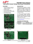
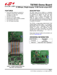
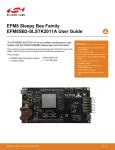
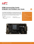
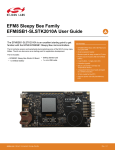
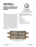
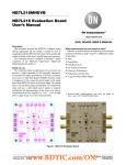
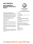
TS7001 Demo Board A Micropower, 2-channel, 187.5-ksps, Serial-Output 12-bit SAR ADC FEATURES DESCRIPTION The demo board for the TS7001 is a completely assembled and tested circuit board that can be used for evaluating the TS7001. For easy and quick evaluation of the TS7001, a Nano River Tech ViperBoard with an on-board microcontroller and FPGA for signal processing is available. The ViperBoard interfaces to any computer via USB port, and user-friendly Windows OS compatible software is available for evaluation. Quick and easy interface to computer for evaluation via Nano River Technologies ViperBoard and USB cable Input BNC connection On-board +3.3V supply voltage On-board TS6001A 2.5V reference voltage External power supply connection available Fully Assembled and Tested 2.2in x 3in 2-layer circuit board The TS7001 – an alternate source for the AD7887 - is a self-contained, 2-channel, high-speed, micropower, 12-bit analog-to-digital converter (ADC) that operates from a single +2.7V to +3.6V power supply. The TS7001 is capable of a 187.5-ksps throughput rate with an external 3MHz serial clock and draws 0.85mA supply current. Product data sheet and additional documentation can be found at www.silabs.com. ORDERING INFORMATION Order Number TS7001DB TSDA-VB Description TS7001 Demo Board Nano River Tech ViperBoard Figure 1. TS7001 Evaluation Board with Nano River Tech Viperboard Figure 2. TS7001 Evaluation Board (Top View) Figure 3. TS7001 Evaluation Board (Bottom View) Page 1 © 2014 Silicon Laboratories, Inc. All rights reserved. TS7001 Demo Board Description The TS7001 demo board provides an easy-to-use scheme for evaluating the TS7001. The default configuration of the demo board in conjunction with the Nano River Tech ViperBoard is for operation at a supply voltage of VDD =+3.3V. The TS7001 demo board includes a 74ALVC164245 signal level translator in order to translate signal levels from VDD of the TS7001 to +3.3V signal voltage levels necessary for the Nano River Tech ViperBoard. The TS7001 and the ViperBoard are connected via an on-board 34-pin socket (X1). A separate power supply can be used to power the TS7001 from +2.7V to +3.6V. The TS7001 demo can be evaluated without the ViperBoard. A BNC connector is available for input AIN0 and AIN1 of the TS7001. It is recommended to use a low-noise signal generator in order to acquire optimal SNR and THD results. The TS7001’s provides one or two analog inputs, AIN0 and AIN1, each with an analog input range from 0 to VREF. In two-channel operation, the analog input range is 0V to VDD. With jumper HDR2, the TS6001A 2.5V external reference or input AIN1 can be selected. Four power management operating modes are available, namely PM Mode 1- PM Mode 4. Refer to Table 2. In two-channel operation and when using the internal reference, modes 1 and 3 allow a maximum sampling rate of 101.69ksps while using the ViperBoard. Figure 5 shows the TS7001 demo board schematic, Figure 2 and Figure 3 show a picture of the top and bottom of the TS7001 demo board, respectively. Figure 1 shows a picture of the TS7001 demo board with the ViperBoard connected. A USB cable is used to interface the ViperBoard to a PC with Windows Vista 32-bit/Vista 64-bit/XP/7. For the “Touchstone ADC Evaluation Platform GUI” user’s manual and for the necessary driver and GUI installer files needed to successfully evaluate the TS7001 with the ViperBoard, please refer to our website at www.silabs.com. Quick Start Procedure Required Equipment TS7001 Demo Board Nano River Technologies ViperBoard USB cable Computer with Windows Vista 32-bit/64-bit/XP/7 ViperBoard driver and GUI software installed to PC( refer to “Touchstone ADC Evaluation Platform GUI” user’s manual) Low-noise Signal Generator Stanford Research Systems Model DS360 or better w/ BNC cable HP 6624A DC Power Supply Khron-Hite Corp Model 526 Precision DC Power Supply In order to evaluate the TS7001, jumper J2 is to be set to position 2-3 and jumper HDR2 is to be left unconnected. The default configuration for J2 and HDR2 is 1-2 and unconnected, respectively. Refer to Figure 5 and Table 1. The default configuration on the board is for VDD = +3.3V. For this evaluation, we will use an external +3.6V power supply and an external +3.6V reference voltage. The following steps are to be performed: 1) Connect the TS7001 demo board ViperBoard via the 34-pin socket (X1). to the 2) With the HP6624A power supply, connect the positive terminal of the power supply to the positive terminal on J1 and the negative terminal of the power supply to the GND terminal of J1. Set the voltage to +3.6V and turn it off. With the Khron-Hite 526 DC power supply, connect the positive terminal of the power supply to terminal 2 on HDR2 and connect the negative terminal of the power supply to the GND terminal of J1. Set the voltage to +3.6V and turn it off. 3) Set the function generator frequency, amplitude, and offset to 10kHz, +3.562VPP, and +1.8V, respectively. Then, connect the BNC cable from the signal generator to the BNC connector AIN0 on the TS7001 demo board. Set the output of the signal generator to OFF. 4) Turn on the power supplies. Page 2 TS7001-EVB Rev. 1.0 TS7001 Demo Board 5) To run the GUI, go to Start > All Programs > TouchStoneEvalBoard 2.2.11 > 01 Touchstone Evaluation App. The GUI should appear and on the top right hand side, the status should be “PC disconnected” and “No Type” for demo board type. Both should be highlighted in red indicating that the Nano River Tech ViperBoard and the TS7001 demo board are not connected. 6) Connect one side of the supplied USB cable to the ViperBoard USB connector. Connect the other side to a USB port on the PC. After approximately three seconds, the status on the GUI screen will switch to “PC Connected” and “TS7001” indicating the ViperBoard and the TS7001 demo board were recognized successfully by the software. The green LED on the TS7001 demo board should be ON and the green LED on the ViperBoard, D2, should be ON. 7) In the TS7001 ADC section, set PM0 = 1 and REF = 1. In the sampling section of the GUI, enter 187.5ksps. Use the default FFT length of 8192. Refer to Figure 4 and Table 2 and Table 3. Additional Functions 9) As shown in the TS7001 ADC section of the GUI, the TS7001 mode of operation can be selected. Please refer to Figure 4 and Table 3. 10) To ensure proper GUI operation, always stop a continuous conversion before changing the state of any of the parameters as described in Table 3. Then, make the necessary jumper connections on the board. Now the parameters can be changed in the GUI according to the connections made on the TS7001 demo board. Then, select continuous to run. 11) To perform a single conversion, press the “single” button in the sampling section. 12) For details on the Touchstone evaluation platform GUI, refer to the “Touchstone ADC Evaluation Platform GUI” user’s manual on our web site at: www.silabs.com. 8) Turn on the signal generator. On the GUI screen, click on “continuous” in the sampling section, and monitor the results on the screen. The top plot shows a samples vs code plot and the bottom plot is an FFT plot. The SNR and THD values should be approximately 71dB and –80dB, respectively. Please refer to Figure 4 for an example of what the results should look like. In this case, the SNR and THD values are 70dB and -80dB,respectively. TS7001-EVB Rev. 1.0 Page 3 TS7001 Demo Board Sampling section TS7001 ADC section Samples vs Code plot FFT plot Figure 4. TS7001 Response with GUI Page 4 TS7001-EVB Rev. 1.0 TS7001 Demo Board Evaluation with TS7001 Demo Board Only Required Equipment TS7001 Demo Board DC Power Supply Low-noise Signal Generator Stanford Research Systems Model DS360 or better w/ BNC cable Ammeter In order to evaluate the TS7001 using the TS7001 demo board only, additional input signals for the തതതത CS SCLK, DIN pins will be necessary along with an oscilloscope to monitor the inputs and output. The following steps are to be performed: 1) Set the voltage of the power supply between +2.7V and +3.6V and turn it off. Connect the positive terminal of the DC power supply to pin 12 labeled as “3.3V” on X1, and the ground terminal to pin 2 labeled as “GND”. Refer to Figure 5. 2) Timing signals for the TS7001 input signals AIN0, AIN1, തതതത CS, DIN, and SCLK should be set according to the desired measurement while following the product datasheet timing specifications. Refer to the TS7001 product data sheet “Timing Specifications”, “TS7001 Control Register Description”, and “Description of Operation” section for details. Access to these pins is available through the 34-pin socket, X1, labeled as “SCLK”, “CS*”, “DIN”, and “DOUT”. The corresponding pins on X1 are 10, 8, 5, and 6, respectively. 3) To measure the supply current of the TS7001, place jumper J2 to position 2-3. Then, apply an external power supply to J1. An ammeter can now be connected in series with the power supply for a static supply current measurement of the TS7001. The supply current should be less than 900µA. Please refer to Figure 5 and table 1. Figure 5. TS7001 Evaluation Board Circuit TS7001-EVB Rev. 1.0 Page 5 TS7001 Demo Board TS7001DB w/ Nano River Tech ViperBoard J1 J2 NA 1-2 (VDD = 3.3V only) +2.7V to +3.6V TS7001 Only NA 2-3 1-2 +2.7V TS7001 Only to 2-3 (Supply Current +3.6V Measurement) Table 1. J1, J2, HDR2, and X1 connections PM1 External Power Supplies 0 (REF = 0) 1 (REF =1) HDR2 X1 Refer to Table 3 34-pin socket 1-2 (two-channel) 2-3 (on-board reference) Unconnected (external reference or internal reference) Apply +2.7 to +3.6V to pin 12 1 (REF = 0) 2 (REF =1) NA NA 1 1 (REF = 0) 2 (REF =1) PM0 Mode PM Mode 1: In this operating mode, the TS7001’s power-down mode is enabled if its CS input is a “one” (a “1”) and is operating in full-power mode 0 0 when its CS input is a “zero” (a “0”). Thus, the TS7001 is powered down on a low-to-high CS transition and is powered up on a high-to-low CS transition. PM Mode 2: In this operating mode and regardless of the status of any of 0 1 the logic inputs, the TS7001 is always fully powered up. PM Mode 3: In this operating mode, the TS7001 is automatically powered down at the end of each conversion regardless of the state of the CS input. 1 0 ADC wake-up time from full shutdown is 5μs and system design should ensure that at least 5μs have elapsed before attempting to perform a conversion in this mode; otherwise, an invalid conversion result may occur. PM Mode 4: In this operating mode, the TS7001 is configured for standby operation after conversion. Sections of the TS7001 are powered down; however, the internal 2.5-V reference voltage remains powered up. While 1 1 PM Mode 4 is similar to PM Mode 3, PM Mode 4 operation allows the TS7001 to power up much faster. For optimal performance, the Control Register’s REF bit (DB5) should be a “zero” (“0”) to ensure the internal reference is enabled/remains enabled. Table 2. TS7001’s Power Management Operating Modes Parameter REF State 0 1 0 SIN/DUAL 1 CH 0 1 Comments Internal 2.5V reference used. Leave jumper HDR2 unconnected. Internal 2.5V reference disabled. External TS6001A 2.5V reference can be used. If REF = 0, Pin 4 is a reference voltage pin and internal 2.5V reference is used. If REF = 1, jumper HDR2 should be set to position 2-3 in order to use external TS6001A 2.5V reference voltage. If REF = 0 or 1, HDR2 is to be set to position 1-2. The device is now in two-channel operation and VDD is used as the reference voltage. AIN0 is selected as the input signal. AIN1 is selected as the input signal. PM1 In modes 1 and 3, the maximum sampling rate is 101.69ksps. Refer to Table 2. PM0 Table 3. TS7001 Parameter States for evaluation with GUI Page 6 TS7001-EVB Rev. 1.0 TS7001 Demo Board DESIGNATION QTY DESCRIPTION C4, C10, C11 3 C12, C13, 2 C5 1 C2, C6 1 C9 1 R16 R15 LED AIN0, AIN1 J1 1 1 1 2 1 X1 J2, HDR2 U2 1 2 1 U1 U3 1 1 0.1µF ±10% capacitor (0603) 10µF ±10% capacitor (SMD6032) 4.7µF ±10% capacitor (SMD6032) 100pF ±10% capacitor (0603) 2.2nF ±10% capacitor (0805) 150Ω± 1% (0603) 1kΩ± 1% (0402) Green LED (0603) BNC connector 2-pin terminal block 34-pin socket Jumper 74ALVC164245 translating transceiver TS6001A TS7001 Table 4. Component list Figure 6. Top Layer Component View Figure 7. Top Layer Trace View Figure 8. Bottom Layer #1 Figure 9. Bottom Layer #2 Silicon Laboratories, Inc. 400 West Cesar Chavez, Austin, TX 78701 +1 (512) 416-8500 ▪ www.silabs.com Page 7 TS7001-EVB Rev. 1.0 Smart. Connected. Energy-Friendly Products Quality Support and Community www.silabs.com/products www.silabs.com/quality community.silabs.com Disclaimer Silicon Laboratories intends to provide customers with the latest, accurate, and in-depth documentation of all peripherals and modules available for system and software implementers using or intending to use the Silicon Laboratories products. Characterization data, available modules and peripherals, memory sizes and memory addresses refer to each specific device, and "Typical" parameters provided can and do vary in different applications. Application examples described herein are for illustrative purposes only. Silicon Laboratories reserves the right to make changes without further notice and limitation to product information, specifications, and descriptions herein, and does not give warranties as to the accuracy or completeness of the included information. Silicon Laboratories shall have no liability for the consequences of use of the information supplied herein. This document does not imply or express copyright licenses granted hereunder to design or fabricate any integrated circuits. The products must not be used within any Life Support System without the specific written consent of Silicon Laboratories. A "Life Support System" is any product or system intended to support or sustain life and/or health, which, if it fails, can be reasonably expected to result in significant personal injury or death. Silicon Laboratories products are generally not intended for military applications. Silicon Laboratories products shall under no circumstances be used in weapons of mass destruction including (but not limited to) nuclear, biological or chemical weapons, or missiles capable of delivering such weapons. Trademark Information Silicon Laboratories Inc., Silicon Laboratories, Silicon Labs, SiLabs and the Silicon Labs logo, CMEMS®, EFM, EFM32, EFR, Energy Micro, Energy Micro logo and combinations thereof, "the world’s most energy friendly microcontrollers", Ember®, EZLink®, EZMac®, EZRadio®, EZRadioPRO®, DSPLL®, ISOmodem ®, Precision32®, ProSLIC®, SiPHY®, USBXpress® and others are trademarks or registered trademarks of Silicon Laboratories Inc. ARM, CORTEX, Cortex-M3 and THUMB are trademarks or registered trademarks of ARM Holdings. Keil is a registered trademark of ARM Limited. All other products or brand names mentioned herein are trademarks of their respective holders. Silicon Laboratories Inc. 400 West Cesar Chavez Austin, TX 78701 USA http://www.silabs.com