1
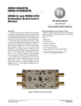
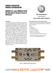
NB4L339MNGEVB
NB4L339MNGEVB
Evaluation Board User's
Manual
http://onsemi.com
EVAL BOARD USER’S MANUAL
INTRODUCTION AND BOARD DESCRIPTION
Layer Stack
ON Semiconductor has developed an evaluation board for
the NB4L339 Clock Generator as a convenience for
customers interested in performing their own device
engineering assessment. The board offers a flexible and
convenient platform to quickly evaluate, characterize and
verify the performance and operation of the NB4L339.
This evaluation board manual contains:
• Information on the NB4L339 Evaluation Board
• Appropriate Lab Setup
• Detailed Board Features
• Bill of Materials
This manual should be used in conjunction with the device
datasheet
(www.onsemi.com/pub/Collateral/NB4L339.PDF), which
contains full technical details on the device specification and
operation.
The NB4L339 Evaluation Board was designed to
accommodate a custom QFN−32 socket. Therefore, some
external components were installed on the bottom side of the
board. SMA connectors are provided for all input & output
signal access.
L1
Signal
L2
SMA Ground
L3
VCC (positive power supply) and VEE (Device
negative power supply)
L4
Signal
Board Features
• Incorporates on−board slide switches to manually
•
•
•
control CLKSEL, DIVSEL, EN and MR logic pins,
minimizing cabling
2.5 V or 3.3 V single or split−power supply operation
LVPECL differential output signals are accessed via
SMA connectors
Convenient and compact board layout
What Measurements Can You Expect to Make?
With this evaluation board, the following measurements
could be performed in single ended or differential modes of
operation.
• Jitter
• Output Skew
• Eye Pattern Generation
• Frequency Performance
• Output Rise and Fall Time
• Phase Noise
Board Layout
The evaluation board is constructed with FR4 material,
provides a high bandwidth 50 W controlled trace impedance
environment and is designed to minimize noise and
minimize crosstalk.
www.BDTIC.com/ON/
© Semiconductor Components Industries, LLC, 2012
February, 2012 − Rev. 1
1
Publication Order Number:
EVBUM2070/D
NB4L339MNGEVB
Top View
Bottom View
Figure 1. NB4L339MNGEVB Evaluation Board
Lab Setup for Time Domain Measurements
Table 1. Basic Lab Equipment
Description
Example Equipment
Qty
Power Supply with 4 outputs
HP6624A
1
Oscilloscope and/or Frequency counter
TDS8000 with 80E01 Sampling Head
1
Differential Signal Generator
Agilent 8133A, Advantest D3186
1
Matched High Speed Cables with SMA Connectors
Storm, Semflex
6 Pair
Digital Voltmeter, Power supply cables
Lab Setup
1. SMAGND (VTT) is the termination supply for the LVPECL outputs
only, not to be confused with the device ground pin (VEE).
A typical lab setup for taking time domain measurements
in differential mode operation is shown in Figure 2. The
following steps should be followed for proper equipment
setup:
Step 2: Connect Inputs
For Differential Mode:
Connect the differential output of the signal generator to
the differential input of the device (CLKx and CLKx). The
differential clock inputs of the NB4L339 incorporate
internal 50 W termination resistors.
For Single−Ended Mode:
Connect the single−ended output of the generator to the
CLKx input of the device. Vth must be applied to the
complementary input (CLKx) when operating in
single−ended mode. Refer to the device datasheet for details
on single−ended operation.
The VTA and VTB termination pins each have a trace
from package pin to a node where it can be connected to
either VCC, VEE or SMAGND, depending on the user’s
need.
NOTE: Inputs CLKA/B and CLKA/CLKB must be
signal driven or auto oscillation may result.
Step 1: Connect Power
Three power levels must be provided to the board, VCC,
VEE, and SMAGND via the banana jack connectors on the
bottom of the board. Bypass capacitors are installed from
VCC to SMAGND and VEE to SMAGND at the banana jacks
and the deivce pins. Using the split power supply mode,
GND = VTT = VCC − 2.0 V. The exposed pad of the QFN−32
package is connected to VEE.
Table 2. NB4L339 Power Supply Connections
3.3 V Setup
VCC = 2.0 V
VCC = 2.0 V
VTT = SMAGND = 0 V
VEE = −1.3 V
2.5 V Setup
VTT = SMAGND = 0 V
VEE = −0.5 V
www.BDTIC.com/ON/
http://onsemi.com
2
NB4L339MNGEVB
Slide Switches
VEE = −1.3 V or −0.5 V
+1.3 V
or
+0.5 V
SMAGND (VTT) = 0 V
CLK
Power Supply
Signal
Generator
CLK
VEE
VCC = 2.0 V
MR
Digital
Oscilliscope
or Frequency
Counter
SMAGND
(VTT)
CLKx
Q
CLKx
Q
CLKSEL
Trigger
+2.0 V
DIVSEL
EN
VCC
Trigger
Figure 2. NB4L339 Board Setup Time Domain (Differential Mode)
NOTE: All differential cable pairs must be matched.
For single−ended operation, CLKx needs to be tied to VTT
through the internal 50 W resistor.
sampling head must have internal 50 W termination to
ground.
NOTE: When single−ended output is being used, the
unconnected output for the pair must be
terminated to VTT through a 50 W resistor for
best operation. Unused outputs pairs may be left
unconnected. Since VTT = 0 V, a standard 50 W
SMA termination is recommended.
Step 3: Setup Input Signals
Set the signal generator output amplitude to 500 mV.
Set the generator output for a square wave clock signal
with a 50% duty cycle.
Step 4: Connect Output Signals
Step 5: Set CLKSEL, DIVSEL, EN and MR
The LVPECL Qxn and Qxn outputs have standard, open
emitter outputs and must be externally DC loaded and AC
terminated. A split power supply technique takes advantage
of terminating the LVPECL outputs into 50 W of an
oscilloscope or a frequency counter. Since VTT = VCC − 2 V,
offsetting VCC to +2.0 V yields VTT = 0 V or Ground
(SMAGND). The VTT terminal connects to the isolated
SMAGND connector ground plane, and is not to be
confused with the device ground pin (VEE).
Connect the Q and Q outputs of the device to the
oscilloscope with matched cables. The oscilloscope
The CLKSEL, DIVSEL, EN and MR control pins can be
controlled from an external source via the appropriate SMA
connector, or using the slide switches located on the board,
as indicated in Figure 2. In order to use the slide switches,
the jumpers/shunts on the bottom side of the board must be
installed. When using an external source, remove the jumper
for that pin. Refer to the NB4L339 datasheet for details on
the proper settings for these pins.
www.BDTIC.com/ON/
http://onsemi.com
3
NB4L339MNGEVB
Figure 3. Frequency Division with the NB4L339
www.BDTIC.com/ON/
http://onsemi.com
4
NB4L339MNGEVB
Figure 4. Evaluation Board Schematic
www.BDTIC.com/ON/
http://onsemi.com
5
NB4L339MNGEVB
Table 3. Detailed board features by device pin.
Pin
Name
Feature
11, 12, 13, 14, 17, 18,
19, 20, 27, 28, 29, 30
Qxn, Qxn
All of the Qxn & Qxn LVPECL outputs have equal length 50 W impedance board
traces with SMA connectors. Matched cables can connect to an oscilloscope or frequency counter.
9, 16, 25, 32
VCC
The VCC pins are all connected directly to the VCC power plane. Bypass capacitors
are installed at each pin.
2, 4, 5, 7
CLKx, CLKx
The CLKx & CLKx Clock input pins have equal length board traces with SMA connectors. Matched cables can connect to a signal generator.
Resistors R1−R4 are intended to terminate a signal generator with 50 W to ground, if
needed. They have been (should be) removed since the NB4L339 already provides
internal 50 W termination resistors for a signal generator when VTx is connected to
SMAGND in a split−power supply configuration.
3, 6
VTA, VTB
10, 31, 15, 26
CLKSEL, DIVSEL,
EN, MR
The VTA and VTB pins each have a trace from package pin to a node where it can
be connected to either VCC, VEE or SMAGND, depending on the user’s need.
Slide Switch Control
The board incorporates slide switches to manually control the logic levels for the
CLKSEL, DIVSEL, EN and MR control pins, thus, minimizing cabling. In order to use
the slide switches, the jumpers/shunts on the bottom side of the board must be installed.
External Control
The CLKSEL, DIVSEL, EN and MR control pins can be controlled from an external
source via the appropriate SMA connector. A 50 W resistor is installed from the trace
to SMAGND to terminate a signal generator, if needed. When using an external
source, remove the switch jumper/shunt from the bottom of the board.
−−
EP
The exposed pad of the QFN−32 package is connected to VEE.
2. NOTE. x = A, B, C, or D; n = 0 or 1
www.BDTIC.com/ON/
http://onsemi.com
6
NB4L339MNGEVB
Table 4. Bill of Materials
Comp
Manufact
Description
Part Number
Qty
Web Site
SMA
Connector
Johnson
SMA Connector, Side
Launch, Gold Plated
142−0711−821
24
www.johnsoncomponents.com
Banana Jack
Deltron
Red Connector Single
PCB Socket
571−0500
1
www.deltron−emcon.com
Banana Jack
Deltron
Black Connector Single
PCB Socket
571−0100
2
www.deltron−emcon.com
Capacitor
AVX Corporation
Cap Cerm .1uF 10%
16V X7R 0603
0603YC104KAT2A
8
www.avxcorp.com
Capacitor
Kemet
Cap Tant 22uF 16V
10% SMD
T491D2236K016AT
2
www.kemet.com
Sliding
Switch
ITT/Cannon
SP3T
OS103011MS8QP1
4
www.ittcannon.com
Jumper
Sullins Electronics
HDR jumper shun
.1CTR
STC02SYAN
4
www.sullinselectronics.com
Jumper
Sullins Electronics
2−pin jumper
PEC36ACN
4
www.sullinselectronics.com
Resistor
Yageo America
Resistor 49.9 Ohm
1/16W 1% 0402 SMD
9C04021A49R9FLMF3
8
www.yageoamerica.com
Evaluation
Board
ON Semiconductor
NB4L339 Evaluation
Board
NB4L339MNGEVB
1
www.onsemi.com
Device
Samples
ON Semiconductor
NB4L339 Clock
Generator
NB4L339MNG
1
www.onsemi.com
Nylon Screw
Standoff
4
Stand off (Height of
Banana Jack)
4
ON Semiconductor and
are registered trademarks of Semiconductor Components Industries, LLC (SCILLC). SCILLC reserves the right to make changes without further notice
to any products herein. SCILLC makes no warranty, representation or guarantee regarding the suitability of its products for any particular purpose, nor does SCILLC assume any liability
arising out of the application or use of any product or circuit, and specifically disclaims any and all liability, including without limitation special, consequential or incidental damages.
“Typical” parameters which may be provided in SCILLC data sheets and/or specifications can and do vary in different applications and actual performance may vary over time. All
operating parameters, including “Typicals” must be validated for each customer application by customer’s technical experts. SCILLC does not convey any license under its patent rights
nor the rights of others. SCILLC products are not designed, intended, or authorized for use as components in systems intended for surgical implant into the body, or other applications
intended to support or sustain life, or for any other application in which the failure of the SCILLC product could create a situation where personal injury or death may occur. Should
Buyer purchase or use SCILLC products for any such unintended or unauthorized application, Buyer shall indemnify and hold SCILLC and its officers, employees, subsidiaries, affiliates,
and distributors harmless against all claims, costs, damages, and expenses, and reasonable attorney fees arising out of, directly or indirectly, any claim of personal injury or death
associated with such unintended or unauthorized use, even if such claim alleges that SCILLC was negligent regarding the design or manufacture of the part. SCILLC is an Equal
Opportunity/Affirmative Action Employer. This literature is subject to all applicable copyright laws and is not for resale in any manner.
PUBLICATION ORDERING INFORMATION
LITERATURE FULFILLMENT:
Literature Distribution Center for ON Semiconductor
P.O. Box 5163, Denver, Colorado 80217 USA
Phone: 303−675−2175 or 800−344−3860 Toll Free USA/Canada
Fax: 303−675−2176 or 800−344−3867 Toll Free USA/Canada
Email: [email protected]
N. American Technical Support: 800−282−9855 Toll Free
USA/Canada
Europe, Middle East and Africa Technical Support:
Phone: 421 33 790 2910
Japan Customer Focus Center
Phone: 81−3−5817−1050
ON Semiconductor Website: www.onsemi.com
Order Literature: http://www.onsemi.com/orderlit
For additional information, please contact your local
Sales Representative
www.BDTIC.com/ON/
http://onsemi.com
7
EVBUM2070/D